EP3468307A1 - Two-wire load control system extension - Google Patents
Two-wire load control system extension Download PDFInfo
- Publication number
- EP3468307A1 EP3468307A1 EP18199468.2A EP18199468A EP3468307A1 EP 3468307 A1 EP3468307 A1 EP 3468307A1 EP 18199468 A EP18199468 A EP 18199468A EP 3468307 A1 EP3468307 A1 EP 3468307A1
- Authority
- EP
- European Patent Office
- Prior art keywords
- load control
- electrical
- power source
- control device
- load
- Prior art date
- Legal status (The legal status is an assumption and is not a legal conclusion. Google has not performed a legal analysis and makes no representation as to the accuracy of the status listed.)
- Granted
Links
- 238000004891 communication Methods 0.000 claims abstract description 71
- 230000002457 bidirectional effect Effects 0.000 claims description 13
- 230000006870 function Effects 0.000 claims description 11
- 239000004065 semiconductor Substances 0.000 claims description 9
- 230000004044 response Effects 0.000 claims description 5
- 230000008713 feedback mechanism Effects 0.000 claims description 2
- 230000002463 transducing effect Effects 0.000 claims description 2
- 230000008901 benefit Effects 0.000 description 15
- 230000001276 controlling effect Effects 0.000 description 10
- 230000008878 coupling Effects 0.000 description 9
- 238000010168 coupling process Methods 0.000 description 9
- 238000005859 coupling reaction Methods 0.000 description 9
- 238000001914 filtration Methods 0.000 description 6
- 238000000034 method Methods 0.000 description 6
- 230000003071 parasitic effect Effects 0.000 description 5
- 230000001419 dependent effect Effects 0.000 description 4
- 238000010616 electrical installation Methods 0.000 description 4
- 238000002955 isolation Methods 0.000 description 4
- 238000010586 diagram Methods 0.000 description 3
- 230000001965 increasing effect Effects 0.000 description 3
- 230000009471 action Effects 0.000 description 2
- 230000000903 blocking effect Effects 0.000 description 2
- 239000003990 capacitor Substances 0.000 description 2
- 230000000694 effects Effects 0.000 description 2
- 239000000463 material Substances 0.000 description 2
- 230000011664 signaling Effects 0.000 description 2
- 230000001960 triggered effect Effects 0.000 description 2
- 230000000007 visual effect Effects 0.000 description 2
- 208000032365 Electromagnetic interference Diseases 0.000 description 1
- XUIMIQQOPSSXEZ-UHFFFAOYSA-N Silicon Chemical compound [Si] XUIMIQQOPSSXEZ-UHFFFAOYSA-N 0.000 description 1
- 230000004913 activation Effects 0.000 description 1
- 230000005540 biological transmission Effects 0.000 description 1
- 230000008859 change Effects 0.000 description 1
- 230000008867 communication pathway Effects 0.000 description 1
- 230000001808 coupling effect Effects 0.000 description 1
- 230000003247 decreasing effect Effects 0.000 description 1
- 238000001514 detection method Methods 0.000 description 1
- 238000009429 electrical wiring Methods 0.000 description 1
- 229910052736 halogen Inorganic materials 0.000 description 1
- 150000002367 halogens Chemical class 0.000 description 1
- 230000001939 inductive effect Effects 0.000 description 1
- 238000009434 installation Methods 0.000 description 1
- 239000012212 insulator Substances 0.000 description 1
- 230000007935 neutral effect Effects 0.000 description 1
- 230000008569 process Effects 0.000 description 1
- 230000009467 reduction Effects 0.000 description 1
- 230000001105 regulatory effect Effects 0.000 description 1
- 238000000926 separation method Methods 0.000 description 1
- 229910052710 silicon Inorganic materials 0.000 description 1
- 239000010703 silicon Substances 0.000 description 1
- 230000005236 sound signal Effects 0.000 description 1
Images


Classifications
-
- H—ELECTRICITY
- H05—ELECTRIC TECHNIQUES NOT OTHERWISE PROVIDED FOR
- H05B—ELECTRIC HEATING; ELECTRIC LIGHT SOURCES NOT OTHERWISE PROVIDED FOR; CIRCUIT ARRANGEMENTS FOR ELECTRIC LIGHT SOURCES, IN GENERAL
- H05B47/00—Circuit arrangements for operating light sources in general, i.e. where the type of light source is not relevant
- H05B47/10—Controlling the light source
- H05B47/175—Controlling the light source by remote control
- H05B47/185—Controlling the light source by remote control via power line carrier transmission
-
- H—ELECTRICITY
- H04—ELECTRIC COMMUNICATION TECHNIQUE
- H04B—TRANSMISSION
- H04B3/00—Line transmission systems
- H04B3/54—Systems for transmission via power distribution lines
-
- H—ELECTRICITY
- H05—ELECTRIC TECHNIQUES NOT OTHERWISE PROVIDED FOR
- H05B—ELECTRIC HEATING; ELECTRIC LIGHT SOURCES NOT OTHERWISE PROVIDED FOR; CIRCUIT ARRANGEMENTS FOR ELECTRIC LIGHT SOURCES, IN GENERAL
- H05B47/00—Circuit arrangements for operating light sources in general, i.e. where the type of light source is not relevant
- H05B47/10—Controlling the light source
- H05B47/165—Controlling the light source following a pre-assigned programmed sequence; Logic control [LC]
-
- Y—GENERAL TAGGING OF NEW TECHNOLOGICAL DEVELOPMENTS; GENERAL TAGGING OF CROSS-SECTIONAL TECHNOLOGIES SPANNING OVER SEVERAL SECTIONS OF THE IPC; TECHNICAL SUBJECTS COVERED BY FORMER USPC CROSS-REFERENCE ART COLLECTIONS [XRACs] AND DIGESTS
- Y02—TECHNOLOGIES OR APPLICATIONS FOR MITIGATION OR ADAPTATION AGAINST CLIMATE CHANGE
- Y02B—CLIMATE CHANGE MITIGATION TECHNOLOGIES RELATED TO BUILDINGS, e.g. HOUSING, HOUSE APPLIANCES OR RELATED END-USER APPLICATIONS
- Y02B20/00—Energy efficient lighting technologies, e.g. halogen lamps or gas discharge lamps
- Y02B20/40—Control techniques providing energy savings, e.g. smart controller or presence detection
Definitions
- the present invention relates to smart load control systems that control the amount of power delivered thereto via smart control devices installed at multiple locations. More particularly, the present invention relates to a smart light dimming system that controls the amount of power delivered to a lighting device in several locations by providing a dimmer device and one or more smart remote extension devices that are operable to communicate with the dimmer device.
- the remote smart load control devices need three wire connections in an electrical installation and it would save material and installation costs if the number of wire connections to remote devices could be decreased. It also discloses that the exchange of information and the charging of active remote circuitry happens for every half-cycle of an AC voltage signal provided by an AC power source coupled to the load control system. As a consequence this limits the available amount of power deliverable to the load which is narrowing the available dimming range.
- the present invention relates to a load control system for controlling the amount of power delivered to an electrical load, the load control system comprising:
- the present invention relates to a load control system for controlling the amount of power delivered to an electrical load.
- the system thereby is especially suitable for allowing control of the amount of power delivered to an electrical load from more than one position, e.g. for dimming a lighting device from different positions in a house.
- the load control system comprises a main load control device connected in series connection between an AC power source and an electrical load, the main load control device providing means for controlling the amount of electrical current flowing from the AC power source through the electrical load.
- the main load control device also is adapted to receive external, electrically signaled messages during a first fraction of a half-cycle of a voltage signal provided by the AC power source.
- the load control system also comprises one or more remote extension devices, which may also be referred to as remote load control extension devices, each of the one or more remote extension devices having not more than two external electrical connection terminals.
- the system thus needs to be adapted for both powering of the remote extension devices as well as allowing control by the remote extension devices through these wires.
- Each of the one or more remote extension devices is being coupled in series connection between the AC power source and the electrical load via the main load control device and is remotely installed from the main load control device.
- the one or more remote extension devices each comprise means for transmitting electrically signaled messages along a communication path during a first fraction of a half-cycle of a voltage signal provided by the AC power source, and the remote extension devices each comprise an internal means for drawing an electrical charging current along a charging path that extends through the main load control device, the electrical charging current being suitable for during a second fraction of a half-cycle of a voltage signal provided by the AC power source supplying electrical power to at least the respective means for transmitting electrically signaled messages.
- the communication path and the charging path use a single switched electrical connection between the main load control device to the remote extension device.
- the second fraction is different from the first fraction.
- the first fraction may be not overlapping with the second fraction.
- the main load control device In response to at least one of the electrically signaled messages transmitted by one of the remote extension devices and received by the main load control device during a first fraction of a half-cycle of a voltage signal provided by the AC power source, the main load control device is adapting the amount of electrical current flowing from the AC power source through the electrical load.
- the first fraction of a half-cycle of a voltage signal provided by the AC power source is a fraction of the positive half-cycle of a voltage signal provided by the AC power source and the second fraction of a half-cycle of a voltage signal provided by the AC power source is a fraction of the negative half-cycle of a voltage signal provided by the AC power source.
- the first fraction and the second fraction may also be interswitched.
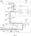
- Fig. 1 shows a schematic block diagram of the load control system 100, e.g. a lighting device control systems, operable from two distinct locations. It comprises the main load control device 101, which may be a dimmer, and an extension load control device 101 thereto, which may be a dimmer too, e.g. a rotary dimmer.
- the electrical wire connection Ext_Ctrl 110, connecting the main load control device 101 and the extension device 102 may serve both as communication path and as charging path as described in the following.
- a load 103 is controlled by the main load control device 101 which is accurately setting the phase angle of a phase control modulator. Hence it is possible to control the gate of a semiconductor switch, e.g.
- a triac two FETs in anti-series connection, or an insulated-gate bipolar junction transistor, which is toggled from a non-conductive state to a conductive state at a tunable time delay after the zero-phase crossing of the AC voltage signal provided by the AC power source. Therefore only a fraction of each half-cycle is relayed, e.g. via a switched line LR 113, to the load 103 thereby regulating the amount of power delivered thereto.
- Detection of the zero-phase crossing may be implemented as part of a synchronization circuit SYNC which is signaling the occurrence of zero-phase crossings to the controller circuit, e.g. to ⁇ C Extension.
- a portion of the trailing edge may be cut, which may be advantageous if capacitive loads instead of resistive or inductive loads are installed.
- the load control system 100 may have the extension device 102 electrically coupled in series between an AC power source via an electrical line L and the main device 101 via an additional wire connection Ext_Ctrl 110, and may have the main control device 101 coupled in series to the controlled load 103, e.g. a lighting device, which is connected back to the AC power source.
- This wire connection Ext_Ctrl 110 establishes both a communication and a charging path, 111 and 112, respectively, between the main load control device 101 and the extension device 102 depending on the polarity of the AC voltage signal provided to the input of the extension device 102 via the electrical line L. It is an advantage of embodiments of the invention that only two wires are necessary to connect the remotely installed extension device 102 to the main load control device 101 without losing the functionality of the remotely installed extension device 102 to act as a dimming control.
- the electrical line L has a positive potential at the input side of the extension device 102 and a current flows into it, if the switch Q1, which may be a bipolar transistor, is open.
- This switch Q1 is operated by a driving circuit, DRIVE, which in turn is controlled by a controller circuit ⁇ C Extension of the extension device 102, which may be a microcontroller, programmable logic device, ASIC, or other appropriate device as it occurs to a person skilled in the art.
- the controller circuit ⁇ C Extension is used to encode a message, that may be a digital message, encoded for instance by the Manchester coding scheme or universal asynchronic receiving transmitting (UART) protocol, by timing the toggling events of the switch Q1 in response to an actuator event triggered by the user, e.g. lowering or increasing the amount of power delivered to the load 103, e.g. lowering or increasing the brightness of a lighting device.
- the digital message is transmitted to and received by the main load control device 101 following the communication path 111.
- a current flow representing the digital message is thereby passing the diode D2 and is directed to the main load control device 101 via the wire connection Ext_Ctrl 110.
- this current continues on the communication path 111 by first passing the diode D5, traversing the coupling element OC1 and the serially connected controlled load 103, e.g. a lighting device, and returning to the AC power source via an electrical line N provided to the load 103. It may be necessary to limit the maximum amount of current of flowing along the communication path 111 and traversing the controlled load 103, for instance a lamp, so as to avoid unwanted flickering or low intensity glowing of the lamp. This may be achieved by a current limiting circuit 114 placed into the communication pathway 111.
- the coupling element OC1 may be an optocoupler and is used to isolate sensitive, e.g.
- a converted part of the transmitted message is output by the coupling element OC1 and provided to a controller circuit, ⁇ C Dimmer, of the main load control device 101, which also may be a microcontroller.
- the controller circuit ⁇ C Dimmer may comprise a receiver circuitry that receives and decodes the transmitted message sent by the extension device 102. As a result thereof the controller circuit ⁇ C Dimmer adjusts the phase angle of the phase control modulator so as to reflect the user input transduced by the respective actuator.
- actuators may include on/off switches, rotary knobs for dimmers, touch panels, push buttons, etc.; the actuators may be supplemented by user-friendly visual or audio feedback information about the current settings, for instance status lamps, LED displays or display bars, audio signal generators.
- the extension device 102 Since the extension device 102 is not equipped with an extra wire connection to the electrical neutral line N, it is not powered separately but requires drawing its supply power through the main load control device 101. This has the advantage of saving an additional wire connection, saves material and costs, and simplifies the electrical installation. As a consequence thereof, the two-wire extension device 102 needs to be charged repeatedly via a charging path 112; the capacitively stored charge is converted into a supply voltage, e.g.
- PSU power supply unit
- the charging path 112 is open during a fraction of the negative half-cycles for which the switched line LR 113 is not energized.
- a charging current flows along the charging path 112 entering the main load control device 101 and being passed by the diode D6. Because of the presence of the diode D5, which is blocking in this configuration, there is not any current flowing through the coupling element OC1 therefore preventing false messaging within the controller circuit ⁇ C Dimmer of the main load control device 101.
- the charging current is then relayed to the extension device 102 via the wire connection Ext_Ctrl 110, passes the diode D3, which prevents the stored charge to be discharged subsequently, and charges storage capacitors that are part of the power supply unit PSU of the extension device 102. Simultaneously the charging path 112 connects to and powers the synchronization circuit SYNC. Exceeding charges of the charging current is leaving the extension device 102 along the diode D1. As for the currents participating in the communication phase being limited where it appears suitable, the charging currents may be current limited as well aiming at reducing the undesired current flow through the load 103. This current limit may be different from the current limit employed during communication.
- Fig. 1 it is also possible to replenish the charge storing devices of the power supply circuitry of the extension device 102 during the positive half-cycles provided that the switch Q1 is open. This implies that even within the communication phase, if the switch Q1 is open by default, and no message is transmitted, the power supply circuitry may be provided with power. This has the advantage that powering of the active circuitry of the extension device 102 is feasible for both positive and negative half-cycles of the AC voltage signal in the absence of communication events, and therefore the charging currents, flowing through the load 103, may be limited even more significantly.
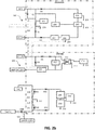
- Fig. 2a to Fig. 2b that illustrate the communication path and powering path for an exemplary embodiment of the invention in a more detailed way compared to what has been shown in Fig. 1 .
- the extension device 102 is shown in Fig. 2a comprising the same building blocks as in Fig. 1 , whereby the communication path is illustrated. It is demonstrated in Fig. 2a that the current flow along the communication path 111, in the event of a message being transmitted, passes through a sensing element, which may be a sensing ohmic resistor Rsense.
- the sensing element represents the amount of current flowing through it, e.g. via an induced voltage drop along its terminals.
- This sensed information is influencing the action of a current limiting circuit, e.g. via a bipolar transistor that interacts with the electronic switch Q1 in such a way that the communication path limits its maximum current rating, e.g. by lowering the base current of a bipolar transistor. It is recommendable to implement switches Q1 with low parasitic capacitances to reduce false triggering events in the receiving circuit of the main load control device 101 due to induced currents originating from the parasitic capacitances.
- the extension device 102 may comprise a pre-regulator circuit, e.g. silicon controlled rectifiers, preceding the power supply units PSU. This may be important if a wider range of AC input signals need to be covered by the extension device 102.
- Fig. 2a also shows a possible current limiting circuit that may be placed inside the main load control device 101, e.g. a dimmer, in order to limit the maximum current rating related to currents that leave the main load control device 101 on the load-sided wire connection, Switched Line, during communication or charging periods and traverse the load 103.
- a filtering circuit e.g. a resistor or an inductor, e.g. a choke, may be coupled in parallel to the coupling element OC1, which may be an opto-coupler, digital isolator, capacitive coupler, or transformer, but is not limited thereto.
- the coupler element OC1 is providing additional isolation between the different electrical circuits of the main load control device 101, in particular it makes isolation with the dimmer circuit ⁇ C Dimmer. This leads for instance to less signal interference between dimmer and extension circuit.
- Fig. 2a also illustrates another part of the main load control device 101 indicating how the communication path 111 is connected to the load-sided terminal of the main load control device 101 via the electrical wire connection, Switched Line, and injects current into the load 103 connected in series with the electrical wire N that is the return path to a coupled AC power source.
- the communication path 111 is connected to the load-sided terminal of the main load control device 101 via the electrical wire connection, Switched Line, and injects current into the load 103 connected in series with the electrical wire N that is the return path to a coupled AC power source.
- FIG. 2a further illustrates a full-bridge rectifying circuit comprising the two diodes D51 and D52, D53 and D54 that each pass a half-cycle of the AC voltage signal provided by the AC power source.
- This half-bridge rectifying circuit may be used to energize a controller circuit, e.g. the dimmer electronics, e.g. a microcontroller ⁇ C dimmer, via suitable choices of pre-regulator and power supply units.
- two instances of parallelly coupled diode-switch pairs, D53/SW1, and D54/SW2, respectively, connected in series, may be provided as a bidirectional semiconductor switch that relays the line-sided terminal 'Line' to the load-sided terminal 'N' of the main load control device 101.
- This bidirectional switch is operated by the controller circuit, e.g. a microcontroller ⁇ C dimmer, so as to allow the main load device to function as a dimmer, for instance to dim a lighting device in a controlled fashion.
- the controller circuit e.g. a microcontroller ⁇ C dimmer
- the switch SW1 is made conductive in response to a signal from the controller circuit, e.g. the dimmer electronic circuits may toggle the switch SW1 to a conductive state at a precise timing, e.g. 2.5 ms after a zero-phase crossing occurred, thus terminating the communication period that takes place during the leading edge, e.g. the first 2.5 ms, of the positive half-cycle.
- the electronic circuits of the main load control device 101 and the extension device 102 may be configured such that the communication period starts within the trailing edge of positive half-cycle of the AC voltage signal, e.g. 2.5 ms before the zero-phase crossing, and the charging period also starts within the trailing edge of the AC voltage signal, e.g. 2.5 ms before the zero-phase crossing, but for a negative half-cycle.
- FIG. 2b illustrates the corresponding powering path for the load system shown in FIG. 2a .
- the communication period and charging period are interchanged, that is the charging period happens during a fraction of a positive half-cycle and the communication period happens during a fraction of a negative half-cycle.
- the communication and charging period may be adapted dynamically as a function of the dimming level, e.g. may range between 0 ms to 5 ms, e.g. between 0 ms and 2.5 ms, or the charging takes place during both positive and negative half-cycles if no message is exchanged, i.e. no communication is required.
- Fig. 2a and Fig. 2b show that sensing elements Rsense1, Rsense2 may be implemented that keep track of the switched load currents.
- the controller circuit e.g.
- the dimmer electronics may then detect changes in the load currents, e.g. disturbances in the AC power signal provided by the source or due to electromagnetic interferences, and compensate for it by influencing the two switches SW1 and SW2.
- the load current sensing may be used to select between different switching or dimming modes that depend on a specific load type. This is advantageous if, for instance, different lighting devices are sought to be compatible with a designed dimming control system and for which different driving protocols are required, e.g. distinguishing between LED, incandescent, and halogen lamps.
- additional switches may be provided, e.g. air-gap switches, that disconnect the entire main load control device 101 or its extension device 102 form the energized AC power line, so that the user may manipulate or change parts within the load control devices without any danger.
- additional switches e.g. air-gap switches, that disconnect the entire main load control device 101 or its extension device 102 form the energized AC power line, so that the user may manipulate or change parts within the load control devices without any danger.
- visual or audio feedback by means of LED status bars, control lamps, or signal generators. This way the user may be informed about the current dimming level, a specific selected operation mode of the load control system 100, e.g. minimum or maximum dimming level reset modes or memory modes, etc.
- the controller circuits of the load control system 100 may comprise a memory element that stores preferred user settings.
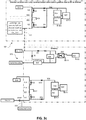
- Fig. 3a to FIG. 3c show a communication path and power path of a load control system similar as shown in FIG. 1 to FIG. 2b , but wherein a dimmer device is configured to work as an extension device 102.
- a dimmer device is configured to work as an extension device 102.
- the main load control device 101 and its extension device 102 are similar or even the same dimming devices, but the second dimmer, is properly configured or set so as to effectively function as an extension device 102.
- Such an embodiment has the particular advantage that only a single hardware needs to be developed for both the main load control device 101 and the extension device 102 and merely the software configuration is set to function as main load control device 101 or extension device 102 accordingly. Referring to Fig. 3a to FIG.
- the diodes D3 and D4 are passing the charging currents of the cut leading or trailing edges of the negative and positive half-cycles of an AC voltage signal provided by an AC power source, respectively. These charging currents are used to load storage capacitances associated with the one or more power supply units PSU, which energize the controller circuitry ⁇ C Extension. More particularly, a cut leading or trailing edge of the negative half-cycle passes the diode D3, charges and energizes the electronics of the second main load control device working as an extension, e.g.
- the dimmer electronics comprising microcontroller and synchronization circuitry, and associated charging currents leave the second main load control device via the electrical line 'Line' after having passed the internal device ground, a sensing resistor, and the diode D1. This describes only the flow of charging current along a charging path 112 within the second main load control device working as an extension device.
- the missing part of the charging path 112 is accomplished by the charging currents associated to the cut leading or trailing edge of the negative half-cycle entering the main load control device 101 by the electrical line 'N', whereby the controlled electrical load 103 is traversed, continuing along the current limiting circuitry 114, passing the diode D6 and reaching the diode D3 of the second load control device acting as an extension via the Ext_Ctrl wire connection.
- the switched line 'LR' 113 of the second load control device acting as an extension to coincide with the Ext_Ctr wire connection terminal, thereby reducing the number of actively used terminals when the device is operational. If the second load control device, e.g.
- the second dimmer device is configured as an extension device 102 care has to be taken to avoid unwanted triggering of the coupling element OC1, e.g. an opto-coupler, during a fraction of the positive half-cycle of the AC power signal leading to wrong messaging between the two connected devices 101, 102.
- the coupling element OC1 e.g. an opto-coupler
- This accidental current path susceptible to induce wrong signaling at the coupler element OC1 may be avoided by a properly designed filter for the coupler element OC1 or a an additional switching element placed in series with the diode D4 of the second load control device acting as an extension and configured so as to block current flow during a positive half-cycle.
- the zero-phase crossings of the leading or trailing edges of the AC voltage signal are detected by the synchronization circuit which is also coupled to the controller circuit ⁇ C Extension and serves as a reference for the precisely timed communication and charging windows during which the load is substantially unpowered.
- Semiconductor switches Q1, Q2, which may be bipolar junction transistors, are driven by a driving circuit, Drive, whose input is provided by signals sent by the controller circuit ⁇ C Extension.
- Simultaneous toggling the switches Q1, Q2 of the second load control device acting as an extension 102 from the on-state to the off-state and vice versa enables the transmission of an encoded message, which may be a digital message, that is directed to the load-sided wire connection, Ext_Ctrl.
- the communication path 111 within the main load control device 101 is identical to what has been described above in embodiments of the invention in connection to Fig. 1 ; in particular it is noted that the communication path is only active during a fraction of the positive half-cycle of the AC power signal.
- the switch Q2 of the second main load control device acting as an extension 102 e.g.
- the second dimmer device acting as a dimmer extension device is by default in an off-state or open position, if not toggled during a communication window, as otherwise charging currents during a fraction of the negative half-cycle may bypass the device's internal circuitry to be charged, e.g. the synchronization or microcontroller circuitry of the second load control device acting as an extension device 102, via a closed switch Q2 and diode D1, and leaving the extension device 102 at its 'Line' terminal.
- the extension device 102 may just be a second main load control device, e.g. a second dimmer device, preceding or following the main load control device 101coupled in a load control system.
- Current limiting circuits 114 may be added to the extension device 102 acting as a dimmer to adjust the maximum current rating during a communication or charging step. This may be advantageous to improve safety and minimize undesirable currents flowing through the load during its substantially unpowered period.
- the dimmer typically comprises dimmer electronics, e.g. a microcontroller of the dimmer, which may comprise a synchronization circuit to determine the right window to send the data, a current limiting circuit, etc.
- the switches Q1 and Q2 advantageously have low parasitic capacitance since these capacitances have the same effect as long cables.
- the switch Q1 opens and closes as function of a communication status and the switch Q2 is always open when the dimmer is configured as extension.
- any unused current can flow during the negative half sine and thus the current flowing during the negative half sine could not be used to foresee the device itself of power.
- the switches Q1 and Q2 are opened and closed at the same time. With respect to powering, power is taken when switches Q1 and Q2are open during the positive half and the negative half. It is to be noted that taking power during the positive half of the sine is tricky because one needs to make sure that OC1 does not get triggered. The latter can be obtained by proper design, such as for example provide a proper filter for the optocoupler. Alternatively, using a switch it could also be designed that only power is taken via the negative half of the sine signal.
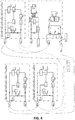
- a plurality of extension devices 102 as illustrated in Fig. 1 may be used simultaneously with and remotely installed from the main load control device 101.
- the plurality of extension devices 102 are connected to each other, and with the AC power source and the controlled electrical load 103 via the main load control device 101. This may be achieved by connecting the electrical line L of a first extension device 102 to the electrical mains, i.e. the AC power source, and by also connecting it to the electrical line L of a second extension device. Additionally the Ext_Ctrl wire connection terminal of the first extension device is connected to the Ext_Ctrl wire connection terminal of the second extension device.
- the electrical line L of the second extension device 102 is connected to the electrical line L of a third extension device and its Ext_Ctrl wire connection terminal is connected to the corresponding one of the third extension device, and so forth.
- the last extension device 102 of the plurality of extension devices has its electrical line L connected to that corresponding to the main load control device 101 and also has its Ext_Ctrl wire connection terminal connected to the one corresponding to the main load control device 101.
- the extension devices 102 are all coupled parallelly in such an alternative embodiment, the communication and charging path still extends through the main load control device 101, e.g. the dimmer device, and through the controlled electrical load 103.
- FIG. 4 illustrates an example of a system with three extensions.
- FIG. 4 also a synchronization circuit is illustrated for the extensions, which is used for determining the right window to send the data.
- switches Q1 it is advantageous that these have a low parasitic capacitance, since such capacitances have the same effect as using long cables.
- a current limiting element is provided, allowing to sense the current e.g. via Rsense and allowing, e.g. via a bipolar transistor, to influence the switch to limit the current.
- a current limiting element may be present and a filtering element.
- the filtering element may for example be a resistor in parallel with the diode, in order to prevent false signals due to capacitive coupling.
- the opto-coupler shown may alternatively be a digital insulator or a capacitive coupler or even a transformer. This element provides isolation to dimmer circuit, so that less interference occurs between the different signals, e.g. the dimmer and the extension.
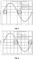
- Fig. 5 illustrates a time window for a 230 Vac voltage signal as provided by an 50 Hz AC power source coupled to the load control system 100.
- the bidirectional switch of the main load control device 101 or the extension device 102 acting as a dimmer is in its non-conducting state. Therefore the voltage across the load, e.g. a light bulb, is substantially zero, whereas the voltage across the main load control device 101 or extension device 102 is following the applied 230 Vac voltage signal and the its internal power supply units are charged such that a constant output voltage, e.g. voltage of the mains, is provided to the communication path 111, e.g.
- No messages are transmitted by either the main load control device 101 or the extension device 102 and charging of the extension device 102 is inactive and the communication path 111/charging path 112 are substantially unenergized.
- the bidirectional switch of the main load control device 101 or the extension device 102 acting as a dimmer is toggled back into its non-conducting state. Therefore the voltage across the main load control device 101 or the extension device 102, e.g. the dimmer, is now following the leading edge of the first negative half-cycle of the 230 Vac voltage signal, whereas substantially no voltage drop occurs across the load 103 during the next 2.5 ms.
- the charging path 112 is energized during a time period tx so as to allow charge currents to flow from the main load control device 101 to the extension device 102 which is replenishing its internal power supply storage capacitances.
- the time period tx may be a variable subject to a dimmer setting from which it is determined.
- the bidirectional switch of the main load control device 101 provides substantially the full 230 Vac voltage signal to the load 103 and leaves the main load control device 101 or the extension device 102, e.g. the dimmer, as well as the communication path 111/charging path 112 unenergized.
- a full period of the 50 Hz source signal has lapsed and the process repeats starting with the second positive half-cycle, followed by the second negative half-cycle, and so on.
- Fig. 6 the same working principle as in Fig. 5 is illustrated except that the communication path 111 is energized at the trailing edge of the positive half-cycle, more particularly for phase angles ranging between 7.5 ms and 10 ms, and that the charging path 112 is energized at the trailing edge of the negative half-cycle, more particularly for phase angles ranging between 17.5 ms and 20 ms.
- This configuration may be preferable for capacitive loads 103.
- the amount of power delivered to the load 103 is below its maximum value, e.g. the brightness of a light bulb is dimmed to some extent, such that the toggling into the conductive state of the bidirectional switch of the main load control device 101 occurs at phase angles that correspond to 5 ms and 15 ms, that is at the middle of each half-cycle.
- the communication path 111 and the charging path 112 may be energized over an extended time period tx that may cover the entire leading edge of the corresponding half-cycles, e.g. a time period that lasts for 5 ms.
- Fig. 8 illustrates the same dynamically adjusted time period during which communication and charging occur in their respective half-cycles.
- the only difference compared to Fig. 7 is that the entire trailing edge of each half-cycle is used to energize the communication path 111 and the charging path 112, respectively.
- Dynamical adjustment of the communication period or charging period tx is advantageous since lower currents may be provided in those cases and the load 103 is disturbed less. If the time periods are increased it may be an option to use redundant encoding so as to achieve error correction or to transmit more data, e.g. more bits of a digital message, during each communication period.
- Fig. 9 the case of a completely dimmed load 103 is shown, in which case the voltage across the load 103 stays substantially zero and the voltage across the dimmer device, e.g. the main load control device 101 or the extension device 102 acting as a dimmer, closely follows the provided 230 Vac voltage signal.
- the charging and communication period tx may both cover the entire AC signal period of 20 ms so as to switch the load 103 back on as quickly as possible if the user operates the related commands.
- the present invention also relates to a remote load control extension device for controlling the amount of power delivered to an electrical load from a second position different from a first position from which the amount of power delivered to an electrical load can also be controlled.
- the remote load control extension device according to embodiments of the present invention comprises not more than two external electrical connection terminals.
- the remote load control extension device is adapted for being coupled in series connection between the AC power source and the electrical load via the main load control device.
- the remote load control extension device furthermore comprises a means for transmitting electrically signaled messages along a communication path during a first fraction of a half-cycle of a voltage signal provided by the AC power source the electrically signaled messages being for controlling the amount of electrical current flowing from the AC power source through the electrical load.
- the remote load control extension device also comprises an internal means for drawing, during a second fraction of a half-cycle of a voltage signal provided by the AC power source, an electrical charging current along a charging path that extends through the main load control device. Such electrical charging current is being suitable for supplying electrical power to at least the respective means for transmitting electrically signaled messages.
- the remote load control extension device further comprises a single port for establishing the communication path and the charging path via a single switched electrical connection between the main load control device to the remote extension device. Further features and advantages may be as described in the first aspect of the present invention.
Landscapes
- Engineering & Computer Science (AREA)
- Power Engineering (AREA)
- Computer Networks & Wireless Communication (AREA)
- Signal Processing (AREA)
- Circuit Arrangement For Electric Light Sources In General (AREA)
Abstract
Description
- The present invention relates to smart load control systems that control the amount of power delivered thereto via smart control devices installed at multiple locations. More particularly, the present invention relates to a smart light dimming system that controls the amount of power delivered to a lighting device in several locations by providing a dimmer device and one or more smart remote extension devices that are operable to communicate with the dimmer device.
- It is common in electrical installations, for instance the electrical wiring in residential buildings, to use interconnected electrical switches to control a load, in many cases a lighting device, from several distinct locations. Well-known examples are two in series connected, but distant single-pole-double-throw (SPDT) light switches either of which can be operated, e.g. upstairs and downstairs in a staircase, so as to turn the lighting device on or off. By inserting one or more intermediate double-pole-double-throw (DPDT) switches in between the two SPDT light switches it is possible to control the lighting device from even more than two locations. In the field of load control systems, especially for lighting applications, it is common practice to use dimmer devices to regulate the amount of power delivered to the load, for instance to regulate the brightness of a LED or other sorts of light sources. In many electrical installations it is desirable to combine a switch and a dimmer into a single device that can be wall-mountable and to dispose of similar second devices placed at multiple remote locations, so as to switch and/or dim a load, e.g. a lighting device, from more than just a single location. For such purposes it is insufficient to serially connect two dimmer devices as synchronization between them is required. In this respect US patent
US 8242708 B2 (Steiner [US] et al.) describes the serial coupling of one smart main load control device and one or more remote smart load control devices in which the smart remote load control devices communicate with the main load control device by transmitting and receiving digital messages via a communication path and in which all the smart load control devices are provided with actuators operated by the user. The remote smart load control devices, however, need three wire connections in an electrical installation and it would save material and installation costs if the number of wire connections to remote devices could be decreased. It also discloses that the exchange of information and the charging of active remote circuitry happens for every half-cycle of an AC voltage signal provided by an AC power source coupled to the load control system. As a consequence this limits the available amount of power deliverable to the load which is narrowing the available dimming range. - It is an object of embodiments of the present invention to provide good systems and methods for controlling an electrical load.
- The above objective is accomplished by a method and device according to the present invention.
- The present invention relates to a load control system for controlling the amount of power delivered to an electrical load, the load control system comprising:
- a main load control device connected in series connection between an AC power source and an electrical load, the main load control device providing means for controlling the amount of electrical current flowing from the AC power source through the electrical load, and the main load control device being adapted to receive external, electrically signaled messages during a first fraction of a half-cycle of a voltage signal provided by the AC power source; and
- one or more remote extension devices, each of the one or more remote extension devices having not more than two external electrical connection terminals and each of the one or more remote extension devices being coupled in series connection between the AC power source and the electrical load via the main load control device and being remotely installed from the main load control device, the one or more remote extension devices each comprising means for transmitting electrically signaled messages along a communication path during a first fraction of a half-cycle of a voltage signal provided by the AC power source, and the remote extension devices comprising each an internal means for drawing, during a second fraction of a half-cycle of a voltage signal provided by the AC power source, the second fraction being different from the first fraction, an electrical charging current along a charging path that extends through at least the main load control device, the electrical charging current being suitable for supplying electrical power to at least the respective means for transmitting electrically signaled messages; and
- wherein the communication path and the charging path use a single switched electrical connection between the main load control device to the remote extension device; and
- wherein in response to at least one of the electrically signaled messages transmitted by one of the remote extension devices and received by the main load control device during a first fraction of a half-cycle of a voltage signal provided by the AC power source, the main load control device is adapting the amount of electrical current flowing from the AC power source through the electrical load.
- Particular and preferred aspects of the invention are set out in the accompanying independent and dependent claims. Features from the dependent claims may be combined with features of the independent claims and with features of other dependent claims as appropriate and not merely as explicitly set out in the claims.
- For purposes of summarizing the invention and the advantages achieved over the prior art, certain objects and advantages of the invention have been described herein above. Of course, it is to be understood that not necessarily all such objects or advantages may be achieved in accordance with any particular embodiment of the invention. Thus, for example, those skilled in the art will recognize that the invention may be embodied or carried out in a manner that achieves or optimizes one advantage or group of advantages as taught herein without necessarily achieving other objects or advantages as may be taught or suggested herein.
- The above and other aspects of the invention will be apparent from and elucidated with reference to the embodiment(s) described hereinafter.
- The invention will now be described further, by way of example, with reference to the accompanying drawings, in which:
-
Fig. 1 shows a block diagram of the load control system and the communication and charging path therein, according to an embodiment of the present invention. -
Fig. 2a andFIG. 2b illustrate the communication path respectively the power path for a load control system as shown inFIG. 1 , according to an embodiment of the present invention. -
FIG. 3a ,FIG. 3b and FIG. 3b illustrate a block diagram of a load control system wherein a dimmer is configured as extension device, whereby inFIG. 3a the communication path is illustrated and inFIG. 3b andFIG. 3c the power path is shown respectively during the negative and positive half of the signal. -
FIG. 4 illustrates an implementation of a system with multiple two-wire extension devices according to an embodiment of the present invention. -
Fig. 5 displays a graph reporting the evolution of the provided AC voltage signal, the voltage across the load, the voltage across the dimmer device, and the voltage levels of the communication and charging paths over a complete cycle with phase control at the leading edges and a conduction phase angle of 7.5 ms. -
Fig. 6 displays a graph reporting the evolution of the provided AC voltage signal, the voltage across the load, the voltage across the dimmer device, and the voltage levels of the communication and charging paths over a complete cycle with phase control at the trailing edges and a conduction phase angle of 7.5 ms. -
Fig. 7 displays a graph reporting the evolution of the provided AC voltage signal, the voltage across the load, the voltage across the dimmer device, and the voltage levels of the communication and charging paths over a complete cycle with phase control at the leading edges and a conduction phase angle of 5 ms. -
Fig. 8 displays a graph reporting the evolution of the provided AC voltage signal, the voltage across the load, the voltage across the dimmer device, and the voltage levels of the communication and charging paths over a complete cycle with phase control at the trailing edges and a conduction phase angle of 5 ms. -
Fig. 9 displays a graph reporting the evolution of the provided AC voltage signal, the voltage across the load, the voltage across the dimmer device, and the voltage levels of the communication and charging paths over a complete cycle for the case of a completely dimmed load. - The drawings are only schematic and are non-limiting. In the drawings, the size of some of the elements may be exaggerated and not drawn on scale for illustrative purposes. The dimensions and the relative dimensions do not necessarily correspond to actual reductions to practice of the invention.
- Any reference signs in the claims shall not be construed as limiting the scope.
- In the different drawings, the same reference signs refer to the same or analogous elements.
- The present invention will be described with respect to particular embodiments and with reference to certain drawings but the invention is not limited thereto but only by the claims.
- The terms first, second and the like in the description and in the claims, are used for distinguishing between similar elements and not necessarily for describing a sequence, either temporally, spatially, in ranking or in any other manner. It is to be understood that the terms so used are interchangeable under appropriate circumstances and that the embodiments of the invention described herein are capable of operation in other sequences than described or illustrated herein.
- Moreover, directional terminology such as top, bottom, front, back, leading, trailing, under, over and the like in the description and the claims is used for descriptive purposes with reference to the orientation of the drawings being described, and not necessarily for describing relative positions. Because components of embodiments of the present invention can be positioned in a number of different orientations, the directional terminology is used for purposes of illustration only, and is in no way intended to be limiting, unless otherwise indicated. It is, hence, to be understood that the terms so used are interchangeable under appropriate circumstances and that the embodiments of the invention described herein are capable of operation in other orientations than described or illustrated herein.
- It is to be noticed that the term "comprising", used in the claims, should not be interpreted as being restricted to the means listed thereafter; it does not exclude other elements or steps. It is thus to be interpreted as specifying the presence of the stated features, integers, steps or components as referred to, but does not preclude the presence or addition of one or more other features, integers, steps or components, or groups thereof. Thus, the scope of the expression "a device comprising means A and B" should not be limited to devices consisting only of components A and B. It means that with respect to the present invention, the only relevant components of the device are A and B.
- Reference throughout this specification to "one embodiment" or "an embodiment" means that a particular feature, structure or characteristic described in connection with the embodiment is included in at least one embodiment of the present invention. Thus, appearances of the phrases "in one embodiment" or "in an embodiment" in various places throughout this specification are not necessarily all referring to the same embodiment, but may. Furthermore, the particular features, structures or characteristics may be combined in any suitable manner, as would be apparent to one of ordinary skill in the art from this disclosure, in one or more embodiments.
- Similarly it should be appreciated that in the description of exemplary embodiments of the invention, various features of the invention are sometimes grouped together in a single embodiment, figure, or description thereof for the purpose of streamlining the disclosure and aiding in the understanding of one or more of the various inventive aspects. This method of disclosure, however, is not to be interpreted as reflecting an intention that the claimed invention requires more features than are expressly recited in each claim. Rather, as the following claims reflect, inventive aspects lie in less than all features of a single foregoing disclosed embodiment. Thus, the claims following the detailed description are hereby expressly incorporated into this detailed description, with each claim standing on its own as a separate embodiment of this invention.
- Furthermore, while some embodiments described herein include some but not other features included in other embodiments, combinations of features of different embodiments are meant to be within the scope of the invention, and form different embodiments, as would be understood by those in the art. For example, in the following claims, any of the claimed embodiments can be used in any combination.
- It should be noted that the use of particular terminology when describing certain features or aspects of the invention should not be taken to imply that the terminology is being re-defined herein to be restricted to include any specific characteristics of the features or aspects of the invention with which that terminology is associated.
- In the description provided herein, numerous specific details are set forth. However, it is understood that embodiments of the invention may be practiced without these specific details. In other instances, well-known methods, structures and techniques have not been shown in detail in order not to obscure an understanding of this description.
- In a first aspect the present invention relates to a load control system for controlling the amount of power delivered to an electrical load. The system thereby is especially suitable for allowing control of the amount of power delivered to an electrical load from more than one position, e.g. for dimming a lighting device from different positions in a house. The load control system comprises a main load control device connected in series connection between an AC power source and an electrical load, the main load control device providing means for controlling the amount of electrical current flowing from the AC power source through the electrical load. According to embodiments of the present invention, the main load control device also is adapted to receive external, electrically signaled messages during a first fraction of a half-cycle of a voltage signal provided by the AC power source.
- The load control system also comprises one or more remote extension devices, which may also be referred to as remote load control extension devices, each of the one or more remote extension devices having not more than two external electrical connection terminals. The system thus needs to be adapted for both powering of the remote extension devices as well as allowing control by the remote extension devices through these wires. Each of the one or more remote extension devices is being coupled in series connection between the AC power source and the electrical load via the main load control device and is remotely installed from the main load control device. The one or more remote extension devices each comprise means for transmitting electrically signaled messages along a communication path during a first fraction of a half-cycle of a voltage signal provided by the AC power source, and the remote extension devices each comprise an internal means for drawing an electrical charging current along a charging path that extends through the main load control device, the electrical charging current being suitable for during a second fraction of a half-cycle of a voltage signal provided by the AC power source supplying electrical power to at least the respective means for transmitting electrically signaled messages. According to embodiments of the present invention, the communication path and the charging path use a single switched electrical connection between the main load control device to the remote extension device.
The second fraction is different from the first fraction. The first fraction may be not overlapping with the second fraction. - In response to at least one of the electrically signaled messages transmitted by one of the remote extension devices and received by the main load control device during a first fraction of a half-cycle of a voltage signal provided by the AC power source, the main load control device is adapting the amount of electrical current flowing from the AC power source through the electrical load. In some embodiments, the first fraction of a half-cycle of a voltage signal provided by the AC power source is a fraction of the positive half-cycle of a voltage signal provided by the AC power source and the second fraction of a half-cycle of a voltage signal provided by the AC power source is a fraction of the negative half-cycle of a voltage signal provided by the AC power source. The first fraction and the second fraction may also be interswitched.
- Further features and advantages will become apparent from the description of the below embodiments and examples, illustrated with reference to the different drawings.
-
Fig. 1 shows a schematic block diagram of theload control system 100, e.g. a lighting device control systems, operable from two distinct locations. It comprises the mainload control device 101, which may be a dimmer, and an extensionload control device 101 thereto, which may be a dimmer too, e.g. a rotary dimmer. According to an embodiment of the invention the electricalwire connection Ext_Ctrl 110, connecting the mainload control device 101 and theextension device 102 may serve both as communication path and as charging path as described in the following. Aload 103 is controlled by the mainload control device 101 which is accurately setting the phase angle of a phase control modulator. Hence it is possible to control the gate of a semiconductor switch, e.g. a triac, two FETs in anti-series connection, or an insulated-gate bipolar junction transistor, which is toggled from a non-conductive state to a conductive state at a tunable time delay after the zero-phase crossing of the AC voltage signal provided by the AC power source. Therefore only a fraction of each half-cycle is relayed, e.g. via a switchedline LR 113, to theload 103 thereby regulating the amount of power delivered thereto. Detection of the zero-phase crossing may be implemented as part of a synchronization circuit SYNC which is signaling the occurrence of zero-phase crossings to the controller circuit, e.g. to µC Extension. Alternatively, instead of cutting a portion of the leading edge of the AC voltage signal, a portion of the trailing edge may be cut, which may be advantageous if capacitive loads instead of resistive or inductive loads are installed. - In operation, the
load control system 100 may have theextension device 102 electrically coupled in series between an AC power source via an electrical line L and themain device 101 via an additionalwire connection Ext_Ctrl 110, and may have themain control device 101 coupled in series to the controlledload 103, e.g. a lighting device, which is connected back to the AC power source. Thiswire connection Ext_Ctrl 110 establishes both a communication and a charging path, 111 and 112, respectively, between the mainload control device 101 and theextension device 102 depending on the polarity of the AC voltage signal provided to the input of theextension device 102 via the electrical line L. It is an advantage of embodiments of the invention that only two wires are necessary to connect the remotely installedextension device 102 to the mainload control device 101 without losing the functionality of the remotely installedextension device 102 to act as a dimming control. - During a fraction of a positive half-cycle of the AC voltage signal provided by the AC power source, the electrical line L has a positive potential at the input side of the
extension device 102 and a current flows into it, if the switch Q1, which may be a bipolar transistor, is open. This switch Q1 is operated by a driving circuit, DRIVE, which in turn is controlled by a controller circuit µC Extension of theextension device 102, which may be a microcontroller, programmable logic device, ASIC, or other appropriate device as it occurs to a person skilled in the art. Therefore the controller circuit µC Extension is used to encode a message, that may be a digital message, encoded for instance by the Manchester coding scheme or universal asynchronic receiving transmitting (UART) protocol, by timing the toggling events of the switch Q1 in response to an actuator event triggered by the user, e.g. lowering or increasing the amount of power delivered to theload 103, e.g. lowering or increasing the brightness of a lighting device. The digital message is transmitted to and received by the mainload control device 101 following thecommunication path 111. A current flow representing the digital message is thereby passing the diode D2 and is directed to the mainload control device 101 via thewire connection Ext_Ctrl 110. Within the mainload control device 101 this current continues on thecommunication path 111 by first passing the diode D5, traversing the coupling element OC1 and the serially connected controlledload 103, e.g. a lighting device, and returning to the AC power source via an electrical line N provided to theload 103. It may be necessary to limit the maximum amount of current of flowing along thecommunication path 111 and traversing the controlledload 103, for instance a lamp, so as to avoid unwanted flickering or low intensity glowing of the lamp. This may be achieved by a current limitingcircuit 114 placed into thecommunication pathway 111. The coupling element OC1 may be an optocoupler and is used to isolate sensitive, e.g. low-voltage devices and circuits, from the higher voltage, energized parts of the mainload control device 101, for instance circuit parts of the mainload control device 101 associated with thecommunication path 111. A converted part of the transmitted message is output by the coupling element OC1 and provided to a controller circuit, µC Dimmer, of the mainload control device 101, which also may be a microcontroller. The controller circuit µC Dimmer may comprise a receiver circuitry that receives and decodes the transmitted message sent by theextension device 102. As a result thereof the controller circuit µC Dimmer adjusts the phase angle of the phase control modulator so as to reflect the user input transduced by the respective actuator. Possible choices of actuators may include on/off switches, rotary knobs for dimmers, touch panels, push buttons, etc.; the actuators may be supplemented by user-friendly visual or audio feedback information about the current settings, for instance status lamps, LED displays or display bars, audio signal generators. - In contrast, no current flows into the
extension device 102 along thecommunication path 111 if the switch Q1 is closed or during a negative half-cycle of the AC voltage signal, since the diode D2 is blocking in this configuration. - Since the
extension device 102 is not equipped with an extra wire connection to the electrical neutral line N, it is not powered separately but requires drawing its supply power through the mainload control device 101. This has the advantage of saving an additional wire connection, saves material and costs, and simplifies the electrical installation. As a consequence thereof, the two-wire extension device 102 needs to be charged repeatedly via a chargingpath 112; the capacitively stored charge is converted into a supply voltage, e.g. a 12V DC voltage or a DC voltage solely determined by the capacitance value of a storage capacitor and by the current limiting of a pre-regulator circuit as a function of the peak voltage value of the electrical mains, by a power supply unit, PSU, which may be an AC-DC converter, powering lower power circuit parts and devices comprised in theextension device 102. It may be advantageous to create multiple supply voltages for different circuit parts, for instance by providing an additional low-dropout voltage supply circuit LDO, e.g. at 3V DC voltage levels, which powers the sensitive controller circuit µC Extension and further protects it by isolation. - In embodiments of the invention according to
Fig. 1 , the chargingpath 112 is open during a fraction of the negative half-cycles for which the switchedline LR 113 is not energized. In this case a charging current flows along the chargingpath 112 entering the mainload control device 101 and being passed by the diode D6. Because of the presence of the diode D5, which is blocking in this configuration, there is not any current flowing through the coupling element OC1 therefore preventing false messaging within the controller circuit µC Dimmer of the mainload control device 101. The charging current is then relayed to theextension device 102 via thewire connection Ext_Ctrl 110, passes the diode D3, which prevents the stored charge to be discharged subsequently, and charges storage capacitors that are part of the power supply unit PSU of theextension device 102. Simultaneously the chargingpath 112 connects to and powers the synchronization circuit SYNC. Exceeding charges of the charging current is leaving theextension device 102 along the diode D1. As for the currents participating in the communication phase being limited where it appears suitable, the charging currents may be current limited as well aiming at reducing the undesired current flow through theload 103. This current limit may be different from the current limit employed during communication. - In embodiments according to
Fig. 1 it is also possible to replenish the charge storing devices of the power supply circuitry of theextension device 102 during the positive half-cycles provided that the switch Q1 is open. This implies that even within the communication phase, if the switch Q1 is open by default, and no message is transmitted, the power supply circuitry may be provided with power. This has the advantage that powering of the active circuitry of theextension device 102 is feasible for both positive and negative half-cycles of the AC voltage signal in the absence of communication events, and therefore the charging currents, flowing through theload 103, may be limited even more significantly. - Reference is now made to
Fig. 2a to Fig. 2b that illustrate the communication path and powering path for an exemplary embodiment of the invention in a more detailed way compared to what has been shown inFig. 1 . Theextension device 102 is shown inFig. 2a comprising the same building blocks as inFig. 1 , whereby the communication path is illustrated. It is demonstrated inFig. 2a that the current flow along thecommunication path 111, in the event of a message being transmitted, passes through a sensing element, which may be a sensing ohmic resistor Rsense. The sensing element represents the amount of current flowing through it, e.g. via an induced voltage drop along its terminals. This sensed information is influencing the action of a current limiting circuit, e.g. via a bipolar transistor that interacts with the electronic switch Q1 in such a way that the communication path limits its maximum current rating, e.g. by lowering the base current of a bipolar transistor. It is recommendable to implement switches Q1 with low parasitic capacitances to reduce false triggering events in the receiving circuit of the mainload control device 101 due to induced currents originating from the parasitic capacitances. Additionally theextension device 102 may comprise a pre-regulator circuit, e.g. silicon controlled rectifiers, preceding the power supply units PSU. This may be important if a wider range of AC input signals need to be covered by theextension device 102. -
Fig. 2a also shows a possible current limiting circuit that may be placed inside the mainload control device 101, e.g. a dimmer, in order to limit the maximum current rating related to currents that leave the mainload control device 101 on the load-sided wire connection, Switched Line, during communication or charging periods and traverse theload 103. A filtering circuit, e.g. a resistor or an inductor, e.g. a choke, may be coupled in parallel to the coupling element OC1, which may be an opto-coupler, digital isolator, capacitive coupler, or transformer, but is not limited thereto. This has the advantage that aforementioned capacitive coupling effects due to parasitic capacitances or due to capacitively coupled, long pairs of cables do not lead to false triggering events in the receiving circuitry, e.g. triggering of an opto-coupler, of the mainload control device 101 or at least mitigates them. The use of the coupler element OC1 is providing additional isolation between the different electrical circuits of the mainload control device 101, in particular it makes isolation with the dimmer circuit µC Dimmer. This leads for instance to less signal interference between dimmer and extension circuit. -
Fig. 2a also illustrates another part of the main load control device 101indicating how thecommunication path 111 is connected to the load-sided terminal of the mainload control device 101 via the electrical wire connection, Switched Line, and injects current into theload 103 connected in series with the electrical wire N that is the return path to a coupled AC power source. Hence it is important to control the amount of current and the time it is emanating from the line 'Switched Line', e.g. by adapting the communication and charging window in terms of phase angles and the use of current limitingcircuits 114 as mentioned beforehand.Fig. 2a further illustrates a full-bridge rectifying circuit comprising the two diodes D51 and D52, D53 and D54 that each pass a half-cycle of the AC voltage signal provided by the AC power source. This half-bridge rectifying circuit may be used to energize a controller circuit, e.g. the dimmer electronics, e.g. a microcontroller µC dimmer, via suitable choices of pre-regulator and power supply units. - As shown in
Fig. 2a two instances of parallelly coupled diode-switch pairs, D53/SW1, and D54/SW2, respectively, connected in series, may be provided as a bidirectional semiconductor switch that relays the line-sided terminal 'Line' to the load-sided terminal 'N' of the mainload control device 101. This bidirectional switch is operated by the controller circuit, e.g. a microcontroller µC dimmer, so as to allow the main load device to function as a dimmer, for instance to dim a lighting device in a controlled fashion. - During a positive half-cycle of the AC voltage signal provided to the 'Line' terminal of the main
load control device 101 the switch SW1 is made conductive in response to a signal from the controller circuit, e.g. the dimmer electronic circuits may toggle the switch SW1 to a conductive state at a precise timing, e.g. 2.5 ms after a zero-phase crossing occurred, thus terminating the communication period that takes place during the leading edge, e.g. the first 2.5 ms, of the positive half-cycle. In alternative embodiments, the electronic circuits of the mainload control device 101 and theextension device 102 may be configured such that the communication period starts within the trailing edge of positive half-cycle of the AC voltage signal, e.g. 2.5 ms before the zero-phase crossing, and the charging period also starts within the trailing edge of the AC voltage signal, e.g. 2.5 ms before the zero-phase crossing, but for a negative half-cycle. -
FIG. 2b illustrates the corresponding powering path for the load system shown inFIG. 2a . - It is also possible that the communication period and charging period are interchanged, that is the charging period happens during a fraction of a positive half-cycle and the communication period happens during a fraction of a negative half-cycle. In still another embodiment, the communication and charging period may be adapted dynamically as a function of the dimming level, e.g. may range between 0 ms to 5 ms, e.g. between 0 ms and 2.5 ms, or the charging takes place during both positive and negative half-cycles if no message is exchanged, i.e. no communication is required. Moreover
Fig. 2a andFig. 2b show that sensing elements Rsense1, Rsense2 may be implemented that keep track of the switched load currents. The controller circuit, e.g. the dimmer electronics, may then detect changes in the load currents, e.g. disturbances in the AC power signal provided by the source or due to electromagnetic interferences, and compensate for it by influencing the two switches SW1 and SW2. Alternatively the load current sensing may be used to select between different switching or dimming modes that depend on a specific load type. This is advantageous if, for instance, different lighting devices are sought to be compatible with a designed dimming control system and for which different driving protocols are required, e.g. distinguishing between LED, incandescent, and halogen lamps. - In embodiments according to the invention additional switches may be provided, e.g. air-gap switches, that disconnect the entire main
load control device 101 or itsextension device 102 form the energized AC power line, so that the user may manipulate or change parts within the load control devices without any danger. Further it is possible to provide for visual or audio feedback by means of LED status bars, control lamps, or signal generators. This way the user may be informed about the current dimming level, a specific selected operation mode of theload control system 100, e.g. minimum or maximum dimming level reset modes or memory modes, etc. For this purpose the controller circuits of theload control system 100 may comprise a memory element that stores preferred user settings. -
Fig. 3a to FIG. 3c show a communication path and power path of a load control system similar as shown inFIG. 1 to FIG. 2b , but wherein a dimmer device is configured to work as anextension device 102. This means that the mainload control device 101 and itsextension device 102 are similar or even the same dimming devices, but the second dimmer, is properly configured or set so as to effectively function as anextension device 102. Such an embodiment has the particular advantage that only a single hardware needs to be developed for both the mainload control device 101 and theextension device 102 and merely the software configuration is set to function as mainload control device 101 orextension device 102 accordingly. Referring toFig. 3a to FIG. 3c , the diodes D3 and D4 are passing the charging currents of the cut leading or trailing edges of the negative and positive half-cycles of an AC voltage signal provided by an AC power source, respectively. These charging currents are used to load storage capacitances associated with the one or more power supply units PSU, which energize the controller circuitry µC Extension. More particularly, a cut leading or trailing edge of the negative half-cycle passes the diode D3, charges and energizes the electronics of the second main load control device working as an extension, e.g. the dimmer electronics comprising microcontroller and synchronization circuitry, and associated charging currents leave the second main load control device via the electrical line 'Line' after having passed the internal device ground, a sensing resistor, and the diode D1. This describes only the flow of charging current along a chargingpath 112 within the second main load control device working as an extension device. The missing part of the chargingpath 112 is accomplished by the charging currents associated to the cut leading or trailing edge of the negative half-cycle entering the mainload control device 101 by the electrical line 'N', whereby the controlledelectrical load 103 is traversed, continuing along the current limitingcircuitry 114, passing the diode D6 and reaching the diode D3 of the second load control device acting as an extension via the Ext_Ctrl wire connection. In embodiments according toFig. 2 , it is preferable to configure the switched line 'LR' 113 of the second load control device acting as an extension to coincide with the Ext_Ctr wire connection terminal, thereby reducing the number of actively used terminals when the device is operational. If the second load control device, e.g. the second dimmer device, is configured as anextension device 102 care has to be taken to avoid unwanted triggering of the coupling element OC1, e.g. an opto-coupler, during a fraction of the positive half-cycle of the AC power signal leading to wrong messaging between the twoconnected devices extension device 102 ground - sensing resistor - diode D2 - switched line 'LR' 113 configured as Ext_Ctrl - diode D5 of the main load control device 101 - coupling element OC1 -current limiting circuitry 114 of the main load control device 101 - switched line 'LR' of the main load control device 101 - electrical line 'N' terminal of the mainload control device 101 thereby also traversing the controlledelectrical load 103. This accidental current path susceptible to induce wrong signaling at the coupler element OC1 may be avoided by a properly designed filter for the coupler element OC1 or a an additional switching element placed in series with the diode D4 of the second load control device acting as an extension and configured so as to block current flow during a positive half-cycle. The zero-phase crossings of the leading or trailing edges of the AC voltage signal are detected by the synchronization circuit which is also coupled to the controller circuit µC Extension and serves as a reference for the precisely timed communication and charging windows during which the load is substantially unpowered. Semiconductor switches Q1, Q2, which may be bipolar junction transistors, are driven by a driving circuit, Drive, whose input is provided by signals sent by the controller circuit µC Extension. Simultaneous toggling the switches Q1, Q2 of the second load control device acting as anextension 102 from the on-state to the off-state and vice versa enables the transmission of an encoded message, which may be a digital message, that is directed to the load-sided wire connection, Ext_Ctrl. Thecommunication path 111 within the mainload control device 101 is identical to what has been described above in embodiments of the invention in connection toFig. 1 ; in particular it is noted that the communication path is only active during a fraction of the positive half-cycle of the AC power signal. Furthermore, it is pointed out that the switch Q2 of the second main load control device acting as anextension 102, e.g. the second dimmer device acting as a dimmer extension device, is by default in an off-state or open position, if not toggled during a communication window, as otherwise charging currents during a fraction of the negative half-cycle may bypass the device's internal circuitry to be charged, e.g. the synchronization or microcontroller circuitry of the second load control device acting as anextension device 102, via a closed switch Q2 and diode D1, and leaving theextension device 102 at its 'Line' terminal. - By way of this example an embodiment of the invention has been described according to which the
extension device 102 may just be a second main load control device, e.g. a second dimmer device, preceding or following the main load control device 101coupled in a load control system. Current limitingcircuits 114 may be added to theextension device 102 acting as a dimmer to adjust the maximum current rating during a communication or charging step. This may be advantageous to improve safety and minimize undesirable currents flowing through the load during its substantially unpowered period. - Both the communication path and the power path respectively during the negative and the positive half of the signal is shown in
FIG. 3a ,FIG. 3b respectivelyFIG. 3c . It is to be noted that current limiting occurs for the communication path.
As shown inFIG. 3a to FIG. 3c , the dimmer typically comprises dimmer electronics, e.g. a microcontroller of the dimmer, which may comprise a synchronization circuit to determine the right window to send the data, a current limiting circuit, etc. The switches Q1 and Q2 advantageously have low parasitic capacitance since these capacitances have the same effect as long cables. The switch Q1 opens and closes as function of a communication status and the switch Q2 is always open when the dimmer is configured as extension. If this switch would not be open, any unused current can flow during the negative half sine and thus the current flowing during the negative half sine could not be used to foresee the device itself of power. During communication, the switches Q1 and Q2 are opened and closed at the same time.
With respect to powering, power is taken when switches Q1 and Q2are open during the positive half and the negative half. It is to be noted that taking power during the positive half of the sine is tricky because one needs to make sure that OC1 does not get triggered. The latter can be obtained by proper design, such as for example provide a proper filter for the optocoupler. Alternatively, using a switch it could also be designed that only power is taken via the negative half of the sine signal. - In alternative embodiments of the invention, a plurality of
extension devices 102 as illustrated inFig. 1 , e.g. up to five extension devices, may be used simultaneously with and remotely installed from the mainload control device 101. In such a particular alternative embodiment, the plurality ofextension devices 102 are connected to each other, and with the AC power source and the controlledelectrical load 103 via the mainload control device 101. This may be achieved by connecting the electrical line L of afirst extension device 102 to the electrical mains, i.e. the AC power source, and by also connecting it to the electrical line L of a second extension device. Additionally the Ext_Ctrl wire connection terminal of the first extension device is connected to the Ext_Ctrl wire connection terminal of the second extension device. Likewise, the electrical line L of thesecond extension device 102 is connected to the electrical line L of a third extension device and its Ext_Ctrl wire connection terminal is connected to the corresponding one of the third extension device, and so forth. Eventually thelast extension device 102 of the plurality of extension devices has its electrical line L connected to that corresponding to the mainload control device 101 and also has its Ext_Ctrl wire connection terminal connected to the one corresponding to the mainload control device 101. Although theextension devices 102 are all coupled parallelly in such an alternative embodiment, the communication and charging path still extends through the mainload control device 101, e.g. the dimmer device, and through the controlledelectrical load 103. By way of illustrationFIG. 4 illustrates an example of a system with three extensions. These only communicate at predetermined time periods. InFIG. 4 , also a synchronization circuit is illustrated for the extensions, which is used for determining the right window to send the data. For switches Q1 it is advantageous that these have a low parasitic capacitance, since such capacitances have the same effect as using long cables. In the extension devices ofFIG. 4 , also a current limiting element is provided, allowing to sense the current e.g. via Rsense and allowing, e.g. via a bipolar transistor, to influence the switch to limit the current. InFIG. 4 it is also shown that in the main dimmer, a current limiting element may be present and a filtering element. The filtering element may for example be a resistor in parallel with the diode, in order to prevent false signals due to capacitive coupling. Furthermore the opto-coupler shown may alternatively be a digital insulator or a capacitive coupler or even a transformer. This element provides isolation to dimmer circuit, so that less interference occurs between the different signals, e.g. the dimmer and the extension. - Further, by way of illustration, embodiments of the present invention not being limited thereto, specific examples of time windows will now be discussed illustrating the timing of the different actions in more detail, thereby illustrating features and advantages of embodiments of the present invention.
-
Fig. 5 illustrates a time window for a 230 Vac voltage signal as provided by an 50 Hz AC power source coupled to theload control system 100. During a leading edge and up to a phase angle corresponding to 2.5 ms the bidirectional switch of the mainload control device 101 or theextension device 102 acting as a dimmer is in its non-conducting state. Therefore the voltage across the load, e.g. a light bulb, is substantially zero, whereas the voltage across the mainload control device 101 orextension device 102 is following the applied 230 Vac voltage signal and the its internal power supply units are charged such that a constant output voltage, e.g. voltage of the mains, is provided to thecommunication path 111, e.g. the voltage across the 'Line'-'Ext_Ctrl' connection, for activation of the communication window At a phase angle corresponding to 2.5 ms after the initial zero-phase crossing the bidirectional switch of the mainload control device 101 or theextension device 102 acting as a dimmer is toggled into its conducting state and the energized 'Line' terminal is connected to the 'Switched Line' and as a consequence thereof no voltage drop occurs across the mainload control device 101 or theextension device 102, e.g. the dimmer. However, the conductive switch now delivers the AC power to theload 103, hence substantially the entire 230 Vac supply voltage is applied across the load. No messages are transmitted by either the mainload control device 101 or theextension device 102 and charging of theextension device 102 is inactive and thecommunication path 111/chargingpath 112 are substantially unenergized. At the zero-phase crossing at the end of the first positive half-cycle corresponding to a phase angle of 10 ms, the bidirectional switch of the mainload control device 101 or theextension device 102 acting as a dimmer is toggled back into its non-conducting state. Therefore the voltage across the mainload control device 101 or theextension device 102, e.g. the dimmer, is now following the leading edge of the first negative half-cycle of the 230 Vac voltage signal, whereas substantially no voltage drop occurs across theload 103 during the next 2.5 ms. However, the chargingpath 112 is energized during a time period tx so as to allow charge currents to flow from the mainload control device 101 to theextension device 102 which is replenishing its internal power supply storage capacitances. The time period tx may be a variable subject to a dimmer setting from which it is determined. At a phase angle corresponding to 12.5 ms the bidirectional switch of the mainload control device 101 provides substantially the full 230 Vac voltage signal to theload 103 and leaves the mainload control device 101 or theextension device 102, e.g. the dimmer, as well as thecommunication path 111/chargingpath 112 unenergized. After 20 ms a full period of the 50 Hz source signal has lapsed and the process repeats starting with the second positive half-cycle, followed by the second negative half-cycle, and so on. - In
Fig. 6 the same working principle as inFig. 5 is illustrated except that thecommunication path 111 is energized at the trailing edge of the positive half-cycle, more particularly for phase angles ranging between 7.5 ms and 10 ms, and that the chargingpath 112 is energized at the trailing edge of the negative half-cycle, more particularly for phase angles ranging between 17.5 ms and 20 ms. This configuration may be preferable for capacitive loads 103. - In
Fig. 7 the amount of power delivered to theload 103 is below its maximum value, e.g. the brightness of a light bulb is dimmed to some extent, such that the toggling into the conductive state of the bidirectional switch of the mainload control device 101 occurs at phase angles that correspond to 5 ms and 15 ms, that is at the middle of each half-cycle. For such a particular embodiment thecommunication path 111 and the chargingpath 112 may be energized over an extended time period tx that may cover the entire leading edge of the corresponding half-cycles, e.g. a time period that lasts for 5 ms. -
Fig. 8 illustrates the same dynamically adjusted time period during which communication and charging occur in their respective half-cycles. The only difference compared toFig. 7 is that the entire trailing edge of each half-cycle is used to energize thecommunication path 111 and the chargingpath 112, respectively. Dynamical adjustment of the communication period or charging period tx is advantageous since lower currents may be provided in those cases and theload 103 is disturbed less. If the time periods are increased it may be an option to use redundant encoding so as to achieve error correction or to transmit more data, e.g. more bits of a digital message, during each communication period. - In
Fig. 9 the case of a completely dimmedload 103 is shown, in which case the voltage across theload 103 stays substantially zero and the voltage across the dimmer device, e.g. the mainload control device 101 or theextension device 102 acting as a dimmer, closely follows the provided 230 Vac voltage signal. In such a particular embodiment the charging and communication period tx may both cover the entire AC signal period of 20 ms so as to switch theload 103 back on as quickly as possible if the user operates the related commands. - In one aspect, the present invention also relates to a remote load control extension device for controlling the amount of power delivered to an electrical load from a second position different from a first position from which the amount of power delivered to an electrical load can also be controlled. The remote load control extension device according to embodiments of the present invention comprises not more than two external electrical connection terminals. The remote load control extension device is adapted for being coupled in series connection between the AC power source and the electrical load via the main load control device. The remote load control extension device furthermore comprises a means for transmitting electrically signaled messages along a communication path during a first fraction of a half-cycle of a voltage signal provided by the AC power source the electrically signaled messages being for controlling the amount of electrical current flowing from the AC power source through the electrical load. The remote load control extension device also comprises an internal means for drawing, during a second fraction of a half-cycle of a voltage signal provided by the AC power source, an electrical charging current along a charging path that extends through the main load control device. Such electrical charging current is being suitable for supplying electrical power to at least the respective means for transmitting electrically signaled messages. The remote load control extension device further comprises a single port for establishing the communication path and the charging path via a single switched electrical connection between the main load control device to the remote extension device. Further features and advantages may be as described in the first aspect of the present invention.
- While the invention has been illustrated and described in detail in the drawings and foregoing description, such illustration and description are to be considered illustrative or exemplary and not restrictive. The foregoing description details certain embodiments of the invention. It will be appreciated, however, that no matter how detailed the foregoing appears in text, the invention may be practiced in many ways. The invention is not limited to the disclosed embodiments.
- Other variations to the disclosed embodiments can be understood and effected by those skilled in the art in practicing the claimed invention, from a study of the drawings, the disclosure and the appended claims. In the claims, the word "comprising" does not exclude other elements or steps, and the indefinite article "a" or "an" does not exclude a plurality. A single processor or other unit may fulfill the functions of several items recited in the claims. The mere fact that certain measures are recited in mutually different dependent claims does not indicate that a combination of these measures cannot be used to advantage. Any reference signs in the claims should not be construed as limiting the scope.
-
- 120
- drive
- 121
- sync
- 122
- PSU AC/DC (12VDC)
- 123
- microcontroller (µC) Extension
- 124
- LDO : 3VDC
- 125
- microcontroller (µC) Dimmer
- 201
- current limiting
- 202
- Rsense
- 203
- Ground extension
- 204
- drive
- 205
- microcontroller (µC) extension
- 206
- synchronisation unit
- 207
- pre-regulator
- 208
- PSU
- 209
- current limiting
- 210
- filtering
- 211
- OC1
- 212
- ground dimmer
- 213
- microcontroller Dimmer
- 214
- SW1
- 215
- Rsense1
- 216
- Rsense2
- 217
- SW2
- 218
- Pre-regulator
- 219
- power supply
- 220
- dimmer electronics, e.g. µC dimmer
- 301
- Rsense3
- 302
- Rsense4
- 303
- Ground Extension
- 304
- UDIM
- 305
- pre-regulator
- 306
- power supply
- 307
- dimmer electronics, e.g. µC dimmer
- 308
- current limiting
- 309
- filtering
- 310
- OC1
- 311
- ground dimmer
- 312
- µC Dimmer
- 313
- SW1
- 314
- Rsense1
- 315
- Rsense2
- 316
- SW2
- 317
- ground dimmer
- 318
- pre-regulator
- 319
- power supply
- 320
- dimmer electronics, e.g. µC dimmer
- 401
- line
- 402
- ext_ctrl
- 403
- Q1
- 404
- Rsense
- 405
- Current limiting
- 406
- ground extension
- 407
- drive
- 408
- pre-regulator
- 409
- PSU
- 410
- Ground Extension
- 411
- synchronisation circuit
- 412
- µC extension
- 413
- switched line
- 414
- current limiting
- 415
- filtering
- 416
- OC1
- 417
- ground dimmer
- 418
- µC dimmer
- 419
- SW1
- 420
- Rsense1
- 421
- Rsense2
- 422
- SW2
- 423
- ground dimmer
- 423
- UDIM
- 424
- pre-regulator
- 425
- power supply
- 426
- dimmer electronics, e.g. µC dimmer
- 427
- Neuter
- 428
- load
The first fraction of a half-cycle of a voltage signal provided by the AC power source may be a fraction of the positive half-cycle of a voltage signal provided by the AC power source and the second fraction of a half-cycle of a voltage signal provided by the AC power source may be a fraction of the negative half-cycle of a voltage signal provided by the AC power source. The first and second fraction also may be interchanged.
The means for controlling the amount of electrical current flowing from the AC power source through the electrical load may comprise a switch, for example a bidirectional semiconductor switch.
The load control system may comprise a controller circuit that is adapted for switching the bidirectional semiconductor switch.
The controller circuit may comprise a microcontroller.
The system may further comprise a synchronization circuit that is adapted for accurately timing the switching of the bidirectional semiconductor switch by the controller circuit.
The load control system may use phase control to control the amount of power delivered to an electrical load.
The electrical charging current along a charging path may be drawn through at least the main load control device during the first and the second fraction of a half-cycle of a voltage signal provided by the AC power source, if no electrically signaled messages are transmitted by any of the remote extension devices.
The one or more remote extension devices may be adapted to receive external, electrically signaled messages during a first fraction of a half-cycle of a voltage signal provided by the AC power source and the main load control device provides means for transmitting electrically signaled messages along a communication path during a first fraction of a half-cycle of a voltage signal provided by the AC power source such that electrically signaled messages are transmitted and received by both the remote extension devices and the main load control device.
One or more main control load devices may be configured as extension device.
The remote extension devices may be rotary-knob dimmers.
The remote extension device may further comprise at least one pre-regulator circuit.
The main load control device may further comprise at least one filter circuit.
The main load control device may be adapted to receive external, electrically signaled messages across an isolating electrical element.
The isolating electrical element may be an optocoupler.
The load control system may further comprise a user control feedback mechanism.
The main control load device and/or remote extension devices may further comprise a switching means for selecting a mode wherein guaranteed no current is flowing through the load. The switching means may be an air-gap switch. In some embodiments, the switching means may be an on/off type switch with a physical air separation, which may for example be used during mounting of loads. The latter may be used to guarantee that no current is flowing through the load at all during for example replacement of a load. The main control load device and/or remote extension devices may in some embodiments comprise a push button or a toggle switch or a rocker switch.
The main load control device may further comprise a memory element.
The memory element may store user preferences for the controlled electrical load and/or preset functions of the controlled electrical load.
The load control system may further comprise actuators for transducing the user control inputs into electrically signaled messages.
The electrically signaled messages may be digital messages using Manchester encoding or universal asynchronic receiving transmitting (UART) protocol.
The first and second fraction of a half-cycle of a voltage signal provided by the AC power source may be dynamically adjustable in time as a function of the amount power delivered to the electrical load.
The present invention also relates to a remote load control extension device for controlling the amount of power delivered to an electrical load from a second position different from a first position from which the amount of power delivered to an electrical load can also be controlled, the remote load control extension device comprising not more than two external electrical connection terminals, and being adapted for being coupled in series connection between the AC power source and the electrical load via the main load control device,
the remote load control extension device furthermore comprising a means for transmitting electrically signaled messages along a communication path during a first fraction of a half-cycle of a voltage signal provided by the AC power source the electrically signaled messages being for controlling the amount of electrical current flowing from the AC power source through the electrical load, and the remote load control extension device comprising an internal means for drawing, during a second fraction of a half-cycle of a voltage signal provided by the AC power source, the second fraction being different from the first fraction, an electrical charging current along a charging path that extends through the main load control device, the electrical charging current being suitable for supplying electrical power to at least the respective means for transmitting electrically signaled messages;
wherein the remote load control extension device comprises a single port for establishing the communication path and the charging path via a single switched electrical connection between the main load control device to the remote extension device.
The first fraction may be not overlapping with the second fraction.
Claims (15)
- A load control system (100) for controlling the amount of power delivered to an electrical load (103), the load control system (100) comprising:- a main load control device (101) connected in series connection between an AC power source and an electrical load (103), the main load control device (101) providing means for controlling the amount of electrical current flowing from the AC power source through the electrical load (103), and the main load control device (101) being adapted to receive external, electrically signaled messages during a first fraction of a half-cycle of a voltage signal provided by the AC power source; and- one or more remote extension devices (102), each of the one or more remote extension devices (102) having not more than two external electrical connection terminals and each of the one or more remote extension devices (102) being coupled in series connection between the AC power source and the electrical load (103) via the main load control device (101) and being remotely installed from the main load control device (101), the one or more remote extension devices (102) each comprising means for transmitting electrically signaled messages along a communication path (111) during a first fraction of a half-cycle of a voltage signal provided by the AC power source, and the remote extension devices (102) comprising each an internal means for drawing, during a second fraction of a half-cycle of a voltage signal provided by the AC power source, the second fraction being different from the first path, an electrical charging current along a charging path (112) that extends through at least the main load control device (101), the electrical charging current being suitable for supplying electrical power to at least the respective means for transmitting electrically signaled messages; and- wherein the communication path (111) and the charging path (112) use a single switched electrical connection (110) between the main load control device (101) to the remote extension device (102); and- wherein in response to at least one of the electrically signaled messages transmitted by one of the remote extension devices (102) and received by the main load control device (101) during a first fraction of a half-cycle of a voltage signal provided by the AC power source, the main load control device (101) is adapting the amount of electrical current flowing from the AC power source through the electrical load (103).
- A load control system (100) according to claim 1, in which the first fraction of a half-cycle of a voltage signal provided by the AC power source is a fraction of the positive half-cycle of a voltage signal provided by the AC power source and the second fraction of a half-cycle of a voltage signal provided by the AC power source is a fraction of the negative half-cycle of a voltage signal provided by the AC power source.
- A load control system (100) according to claim 1 or 2, in which the means for controlling the amount of electrical current flowing from the AC power source through the electrical load (103) comprise a switch, e.g. a bidirectional semiconductor switch.
- A load control system (100) according to claim 3, further comprising a controller circuit that is adapted for switching the bidirectional semiconductor switch and/or a controller circuit comprising a microcontroller.
- A load control system (100) according to claim 4, further comprising a synchronization circuit that is adapted for accurately timing the switching of the bidirectional semiconductor switch by the controller circuit.
- A load control system (100) according to claim 5 which uses phase control to control the amount of power delivered to an electrical load (103).
- A load control system (100) according to any of the previous claims, in which the electrical charging current along a charging path (112) are drawn through at least the main load control device (101) during the first and the second fraction of a half-cycle of a voltage signal provided by the AC power source, if no electrically signaled messages are transmitted by any of the remote extension devices (102).
- A load control system (100) according to any of the previous claims, in which the remote extension devices (102) are adapted to receive external, electrically signaled messages during a first fraction of a half-cycle of a voltage signal provided by the AC power source and the main load control device (101) provides means for transmitting electrically signaled messages along a communication path (111) during a first fraction of a half-cycle of a voltage signal provided by the AC power source such that electrically signaled messages are transmitted and received by both the remote extension devices (102) and the main load control device (101).
- A load control system (100) according to claim 8, in which one or more main control load devices are configured as remote extension devices (102) and/or in which the remote extension devices (102) are rotary-knob dimmers and/or in which the remote extension device (102) further comprises at least one pre-regulator circuit.
- A load control system (100) according to any of the previous claims, in which the main load control device (101) further comprises at least one filter circuit and/or in which the main load control device (101) is adapted to receive external, electrically signaled messages across an isolating electrical element, e.g. an optocoupler and/or wherein the load control system (100) further comprises a user control feedback mechanism and/or actuators for transducing the user control inputs into electrically signaled messages.
- A load control system (100) according to any of the previous claims, in which the main control load device (101) and/or remote extension devices (102) further comprise a switching means for selecting a mode wherein guaranteed no current is flowing through the load and/or in which the main load control device (101) further comprises a memory element for storing user preferences for the controlled electrical load (103) and/or preset functions of the controlled electrical load (103).
- A load control system (100) according to any of the previous claims, in which the first and second fraction of a half-cycle of a voltage signal provided by the AC power source are dynamically adjustable in time as a function of the amount power delivered to the electrical load (103).
- A remote load control extension device (101) for controlling the amount of power delivered to an electrical load (103) from a second position different from a first position from which the amount of power delivered to an electrical load can also be controlled,
the remote load control extension device (101) comprising not more than two external electrical connection terminals, and being adapted for being coupled in series connection between the AC power source and the electrical load (103) via the main load control device,
the remote load control extension device (101) furthermore comprising a means for transmitting electrically signaled messages along a communication path (111) during a first fraction of a half-cycle of a voltage signal provided by the AC power source the electrically signaled messages being for controlling the amount of electrical current flowing from the AC power source through the electrical load (103), and the remote load control extension device (101) comprising an internal means for drawing, during a second fraction of a half-cycle of a voltage signal provided by the AC power source, the second fraction being different from the first fraction, an electrical charging current along a charging path (112) that extends through the main load control device (101), the electrical charging current being suitable for supplying electrical power to at least the respective means for transmitting electrically signaled messages;
wherein the remote load control extension device (101) comprises a single port for establishing the communication path (111) and the charging path (112) via a single switched electrical connection (110) between the main load control device (101) to the remote extension device (102). - Use of a system according to any of claims 1 to 12, for controlling the amount of power delivered to an electrical load.
- Use of a remote load control extension device according to claim 13, for upgrading a load control system for controlling the amount of power delivered to an electrical load from more than one location.
Applications Claiming Priority (1)
| Application Number | Priority Date | Filing Date | Title |
|---|---|---|---|
| BE2017/5724A BE1025630B1 (en) | 2017-10-09 | 2017-10-09 | Extension for a 2-wire ballast control system |
Publications (2)
| Publication Number | Publication Date |
|---|---|
| EP3468307A1 true EP3468307A1 (en) | 2019-04-10 |
| EP3468307B1 EP3468307B1 (en) | 2022-11-30 |
Family
ID=60990537
Family Applications (1)
| Application Number | Title | Priority Date | Filing Date |
|---|---|---|---|
| EP18199468.2A Active EP3468307B1 (en) | 2017-10-09 | 2018-10-09 | Two-wire load control system extension |
Country Status (4)
| Country | Link |
|---|---|
| EP (1) | EP3468307B1 (en) |
| BE (1) | BE1025630B1 (en) |
| DK (1) | DK3468307T3 (en) |
| PL (1) | PL3468307T3 (en) |
Citations (5)
| Publication number | Priority date | Publication date | Assignee | Title |
|---|---|---|---|---|
| US20040207343A1 (en) * | 2003-04-18 | 2004-10-21 | Novikov Lenny M. | Dimmer control system with tandem power supplies |
| US20090206769A1 (en) * | 2008-02-19 | 2009-08-20 | Lutron Electronics Co., Inc. | Smart Load Control Device Having a Rotary Actuator |
| US7872377B2 (en) * | 2009-01-15 | 2011-01-18 | Wilson Phillip C | Communications in multiple-switch electrical circuits |
| US8242708B2 (en) | 2007-04-23 | 2012-08-14 | Lutron Electronics Co., Inc. | Multiple location load control system |
| EP2033495B1 (en) * | 2006-06-22 | 2013-04-24 | Lutron Electronics Co., Inc. | Multiple location dimming system |
Family Cites Families (1)
| Publication number | Priority date | Publication date | Assignee | Title |
|---|---|---|---|---|
| US8294556B2 (en) * | 2007-04-17 | 2012-10-23 | Powerline Control Systems, Inc. | Powerline control system and method |
-
2017
- 2017-10-09 BE BE2017/5724A patent/BE1025630B1/en active IP Right Grant
-
2018
- 2018-10-09 EP EP18199468.2A patent/EP3468307B1/en active Active
- 2018-10-09 DK DK18199468.2T patent/DK3468307T3/en active
- 2018-10-09 PL PL18199468.2T patent/PL3468307T3/en unknown
Patent Citations (5)
| Publication number | Priority date | Publication date | Assignee | Title |
|---|---|---|---|---|
| US20040207343A1 (en) * | 2003-04-18 | 2004-10-21 | Novikov Lenny M. | Dimmer control system with tandem power supplies |
| EP2033495B1 (en) * | 2006-06-22 | 2013-04-24 | Lutron Electronics Co., Inc. | Multiple location dimming system |
| US8242708B2 (en) | 2007-04-23 | 2012-08-14 | Lutron Electronics Co., Inc. | Multiple location load control system |
| US20090206769A1 (en) * | 2008-02-19 | 2009-08-20 | Lutron Electronics Co., Inc. | Smart Load Control Device Having a Rotary Actuator |
| US7872377B2 (en) * | 2009-01-15 | 2011-01-18 | Wilson Phillip C | Communications in multiple-switch electrical circuits |
Also Published As
| Publication number | Publication date |
|---|---|
| BE1025630A1 (en) | 2019-05-03 |
| PL3468307T3 (en) | 2023-01-09 |
| BE1025630B1 (en) | 2019-05-09 |
| EP3468307B1 (en) | 2022-11-30 |
| DK3468307T3 (en) | 2022-12-19 |
Similar Documents
| Publication | Publication Date | Title |
|---|---|---|
| US11558939B2 (en) | Multiple location load control system | |
| CN108432347B (en) | Multi-position load control system | |
| US9521728B2 (en) | Multiple location load control system | |
| US7723925B2 (en) | Multiple location dimming system | |
| US7687940B2 (en) | Dimmer switch for use with lighting circuits having three-way switches | |
| US8729814B2 (en) | Two-wire analog FET-based dimmer switch | |
| US7830042B2 (en) | Dimmer switch for use with lighting circuits having three-way switches | |
| US8212425B2 (en) | Lighting control device for use with lighting circuits having three-way switches | |
| US20060273775A1 (en) | Power supply for a load control device | |
| WO2009027963A2 (en) | Remote controlled electrical switch retrofit system | |
| EP3468307B1 (en) | Two-wire load control system extension |
Legal Events
| Date | Code | Title | Description |
|---|---|---|---|
| PUAI | Public reference made under article 153(3) epc to a published international application that has entered the european phase |
Free format text: ORIGINAL CODE: 0009012 |
|
| STAA | Information on the status of an ep patent application or granted ep patent |
Free format text: STATUS: THE APPLICATION HAS BEEN PUBLISHED |
|
| AK | Designated contracting states |
Kind code of ref document: A1 Designated state(s): AL AT BE BG CH CY CZ DE DK EE ES FI FR GB GR HR HU IE IS IT LI LT LU LV MC MK MT NL NO PL PT RO RS SE SI SK SM TR |
|
| AX | Request for extension of the european patent |
Extension state: BA ME |
|
| STAA | Information on the status of an ep patent application or granted ep patent |
Free format text: STATUS: REQUEST FOR EXAMINATION WAS MADE |
|
| 17P | Request for examination filed |
Effective date: 20191010 |
|
| RBV | Designated contracting states (corrected) |
Designated state(s): AL AT BE BG CH CY CZ DE DK EE ES FI FR GB GR HR HU IE IS IT LI LT LU LV MC MK MT NL NO PL PT RO RS SE SI SK SM TR |
|
| STAA | Information on the status of an ep patent application or granted ep patent |
Free format text: STATUS: EXAMINATION IS IN PROGRESS |
|
| STAA | Information on the status of an ep patent application or granted ep patent |
Free format text: STATUS: EXAMINATION IS IN PROGRESS |
|
| 17Q | First examination report despatched |
Effective date: 20200727 |
|
| STAA | Information on the status of an ep patent application or granted ep patent |
Free format text: STATUS: EXAMINATION IS IN PROGRESS |
|
| REG | Reference to a national code |
Ref country code: DE Ref legal event code: R079 Ref document number: 602018043574 Country of ref document: DE Free format text: PREVIOUS MAIN CLASS: H05B0037020000 Ipc: H05B0047100000 |
|
| GRAP | Despatch of communication of intention to grant a patent |
Free format text: ORIGINAL CODE: EPIDOSNIGR1 |
|
| STAA | Information on the status of an ep patent application or granted ep patent |
Free format text: STATUS: GRANT OF PATENT IS INTENDED |
|
| RIC1 | Information provided on ipc code assigned before grant |
Ipc: H04B 3/54 20060101ALI20220525BHEP Ipc: H05B 47/185 20200101ALI20220525BHEP Ipc: H05B 47/10 20200101AFI20220525BHEP |
|
| INTG | Intention to grant announced |
Effective date: 20220624 |
|
| GRAS | Grant fee paid |
Free format text: ORIGINAL CODE: EPIDOSNIGR3 |
|
| GRAA | (expected) grant |
Free format text: ORIGINAL CODE: 0009210 |
|
| STAA | Information on the status of an ep patent application or granted ep patent |
Free format text: STATUS: THE PATENT HAS BEEN GRANTED |
|
| AK | Designated contracting states |
Kind code of ref document: B1 Designated state(s): AL AT BE BG CH CY CZ DE DK EE ES FI FR GB GR HR HU IE IS IT LI LT LU LV MC MK MT NL NO PL PT RO RS SE SI SK SM TR |
|
| REG | Reference to a national code |
Ref country code: CH Ref legal event code: EP Ref country code: GB Ref legal event code: FG4D |
|
| REG | Reference to a national code |
Ref country code: AT Ref legal event code: REF Ref document number: 1535707 Country of ref document: AT Kind code of ref document: T Effective date: 20221215 |
|
| REG | Reference to a national code |
Ref country code: DK Ref legal event code: T3 Effective date: 20221216 |
|
| REG | Reference to a national code |
Ref country code: IE Ref legal event code: FG4D |
|
| REG | Reference to a national code |
Ref country code: DE Ref legal event code: R096 Ref document number: 602018043574 Country of ref document: DE |
|
| REG | Reference to a national code |
Ref country code: NO Ref legal event code: T2 Effective date: 20221130 |
|
| REG | Reference to a national code |
Ref country code: NL Ref legal event code: FP |
|
| REG | Reference to a national code |
Ref country code: SE Ref legal event code: TRGR |
|
| REG | Reference to a national code |
Ref country code: SK Ref legal event code: T3 Ref document number: E 40931 Country of ref document: SK |
|
| REG | Reference to a national code |
Ref country code: LT Ref legal event code: MG9D |
|
| PG25 | Lapsed in a contracting state [announced via postgrant information from national office to epo] |
Ref country code: PT Free format text: LAPSE BECAUSE OF FAILURE TO SUBMIT A TRANSLATION OF THE DESCRIPTION OR TO PAY THE FEE WITHIN THE PRESCRIBED TIME-LIMIT Effective date: 20230331 Ref country code: LT Free format text: LAPSE BECAUSE OF FAILURE TO SUBMIT A TRANSLATION OF THE DESCRIPTION OR TO PAY THE FEE WITHIN THE PRESCRIBED TIME-LIMIT Effective date: 20221130 Ref country code: FI Free format text: LAPSE BECAUSE OF FAILURE TO SUBMIT A TRANSLATION OF THE DESCRIPTION OR TO PAY THE FEE WITHIN THE PRESCRIBED TIME-LIMIT Effective date: 20221130 Ref country code: ES Free format text: LAPSE BECAUSE OF FAILURE TO SUBMIT A TRANSLATION OF THE DESCRIPTION OR TO PAY THE FEE WITHIN THE PRESCRIBED TIME-LIMIT Effective date: 20221130 |
|
| PG25 | Lapsed in a contracting state [announced via postgrant information from national office to epo] |
Ref country code: RS Free format text: LAPSE BECAUSE OF FAILURE TO SUBMIT A TRANSLATION OF THE DESCRIPTION OR TO PAY THE FEE WITHIN THE PRESCRIBED TIME-LIMIT Effective date: 20221130 Ref country code: LV Free format text: LAPSE BECAUSE OF FAILURE TO SUBMIT A TRANSLATION OF THE DESCRIPTION OR TO PAY THE FEE WITHIN THE PRESCRIBED TIME-LIMIT Effective date: 20221130 Ref country code: IS Free format text: LAPSE BECAUSE OF FAILURE TO SUBMIT A TRANSLATION OF THE DESCRIPTION OR TO PAY THE FEE WITHIN THE PRESCRIBED TIME-LIMIT Effective date: 20230330 Ref country code: HR Free format text: LAPSE BECAUSE OF FAILURE TO SUBMIT A TRANSLATION OF THE DESCRIPTION OR TO PAY THE FEE WITHIN THE PRESCRIBED TIME-LIMIT Effective date: 20221130 Ref country code: GR Free format text: LAPSE BECAUSE OF FAILURE TO SUBMIT A TRANSLATION OF THE DESCRIPTION OR TO PAY THE FEE WITHIN THE PRESCRIBED TIME-LIMIT Effective date: 20230301 |
|
| P01 | Opt-out of the competence of the unified patent court (upc) registered |
Effective date: 20230526 |
|
| PG25 | Lapsed in a contracting state [announced via postgrant information from national office to epo] |
Ref country code: SM Free format text: LAPSE BECAUSE OF FAILURE TO SUBMIT A TRANSLATION OF THE DESCRIPTION OR TO PAY THE FEE WITHIN THE PRESCRIBED TIME-LIMIT Effective date: 20221130 Ref country code: RO Free format text: LAPSE BECAUSE OF FAILURE TO SUBMIT A TRANSLATION OF THE DESCRIPTION OR TO PAY THE FEE WITHIN THE PRESCRIBED TIME-LIMIT Effective date: 20221130 Ref country code: EE Free format text: LAPSE BECAUSE OF FAILURE TO SUBMIT A TRANSLATION OF THE DESCRIPTION OR TO PAY THE FEE WITHIN THE PRESCRIBED TIME-LIMIT Effective date: 20221130 Ref country code: CZ Free format text: LAPSE BECAUSE OF FAILURE TO SUBMIT A TRANSLATION OF THE DESCRIPTION OR TO PAY THE FEE WITHIN THE PRESCRIBED TIME-LIMIT Effective date: 20221130 |
|
| PG25 | Lapsed in a contracting state [announced via postgrant information from national office to epo] |
Ref country code: AL Free format text: LAPSE BECAUSE OF FAILURE TO SUBMIT A TRANSLATION OF THE DESCRIPTION OR TO PAY THE FEE WITHIN THE PRESCRIBED TIME-LIMIT Effective date: 20221130 |
|
| REG | Reference to a national code |
Ref country code: DE Ref legal event code: R097 Ref document number: 602018043574 Country of ref document: DE |
|
| PLBE | No opposition filed within time limit |
Free format text: ORIGINAL CODE: 0009261 |
|
| STAA | Information on the status of an ep patent application or granted ep patent |
Free format text: STATUS: NO OPPOSITION FILED WITHIN TIME LIMIT |
|
| 26N | No opposition filed |
Effective date: 20230831 |
|
| PG25 | Lapsed in a contracting state [announced via postgrant information from national office to epo] |
Ref country code: SI Free format text: LAPSE BECAUSE OF FAILURE TO SUBMIT A TRANSLATION OF THE DESCRIPTION OR TO PAY THE FEE WITHIN THE PRESCRIBED TIME-LIMIT Effective date: 20221130 |
|
| PGFP | Annual fee paid to national office [announced via postgrant information from national office to epo] |
Ref country code: PL Payment date: 20230922 Year of fee payment: 6 Ref country code: NL Payment date: 20231019 Year of fee payment: 6 |
|
| REG | Reference to a national code |
Ref country code: AT Ref legal event code: UEP Ref document number: 1535707 Country of ref document: AT Kind code of ref document: T Effective date: 20221130 |
|
| PGFP | Annual fee paid to national office [announced via postgrant information from national office to epo] |
Ref country code: SK Payment date: 20231005 Year of fee payment: 6 |
|
| PGFP | Annual fee paid to national office [announced via postgrant information from national office to epo] |
Ref country code: GB Payment date: 20231020 Year of fee payment: 6 |
|
| PGFP | Annual fee paid to national office [announced via postgrant information from national office to epo] |
Ref country code: SE Payment date: 20231019 Year of fee payment: 6 Ref country code: NO Payment date: 20231025 Year of fee payment: 6 Ref country code: IT Payment date: 20231026 Year of fee payment: 6 Ref country code: FR Payment date: 20231026 Year of fee payment: 6 Ref country code: DK Payment date: 20231024 Year of fee payment: 6 Ref country code: DE Payment date: 20231020 Year of fee payment: 6 Ref country code: CH Payment date: 20231102 Year of fee payment: 6 Ref country code: AT Payment date: 20231020 Year of fee payment: 6 |
|
| PGFP | Annual fee paid to national office [announced via postgrant information from national office to epo] |
Ref country code: BE Payment date: 20231019 Year of fee payment: 6 |