EP3467152A1 - Surface treatment material, production method thereof, and component formed using surface treatment material - Google Patents
Surface treatment material, production method thereof, and component formed using surface treatment material Download PDFInfo
- Publication number
- EP3467152A1 EP3467152A1 EP17806829.2A EP17806829A EP3467152A1 EP 3467152 A1 EP3467152 A1 EP 3467152A1 EP 17806829 A EP17806829 A EP 17806829A EP 3467152 A1 EP3467152 A1 EP 3467152A1
- Authority
- EP
- European Patent Office
- Prior art keywords
- zinc
- treated material
- conductive substrate
- layer
- alloy
- Prior art date
- Legal status (The legal status is an assumption and is not a legal conclusion. Google has not performed a legal analysis and makes no representation as to the accuracy of the status listed.)
- Withdrawn
Links
- 239000000463 material Substances 0.000 title claims abstract description 111
- 238000004381 surface treatment Methods 0.000 title claims abstract description 107
- 238000004519 manufacturing process Methods 0.000 title claims description 13
- 239000011701 zinc Substances 0.000 claims abstract description 171
- 229910052725 zinc Inorganic materials 0.000 claims abstract description 171
- HCHKCACWOHOZIP-UHFFFAOYSA-N Zinc Chemical compound [Zn] HCHKCACWOHOZIP-UHFFFAOYSA-N 0.000 claims abstract description 170
- 239000000758 substrate Substances 0.000 claims abstract description 145
- 238000007747 plating Methods 0.000 claims abstract description 117
- 229910052751 metal Inorganic materials 0.000 claims abstract description 44
- 239000002184 metal Substances 0.000 claims abstract description 44
- 238000012360 testing method Methods 0.000 claims abstract description 17
- 238000010998 test method Methods 0.000 claims abstract description 9
- PXHVJJICTQNCMI-UHFFFAOYSA-N Nickel Chemical compound [Ni] PXHVJJICTQNCMI-UHFFFAOYSA-N 0.000 claims description 108
- 230000004913 activation Effects 0.000 claims description 50
- 229910052759 nickel Inorganic materials 0.000 claims description 41
- 229910052782 aluminium Inorganic materials 0.000 claims description 33
- XAGFODPZIPBFFR-UHFFFAOYSA-N aluminium Chemical group [Al] XAGFODPZIPBFFR-UHFFFAOYSA-N 0.000 claims description 31
- 238000000034 method Methods 0.000 claims description 31
- 239000010931 gold Substances 0.000 claims description 29
- KDLHZDBZIXYQEI-UHFFFAOYSA-N Palladium Chemical compound [Pd] KDLHZDBZIXYQEI-UHFFFAOYSA-N 0.000 claims description 20
- KRHYYFGTRYWZRS-UHFFFAOYSA-N Fluorane Chemical compound F KRHYYFGTRYWZRS-UHFFFAOYSA-N 0.000 claims description 18
- 238000006467 substitution reaction Methods 0.000 claims description 17
- QAOWNCQODCNURD-UHFFFAOYSA-N Sulfuric acid Chemical compound OS(O)(=O)=O QAOWNCQODCNURD-UHFFFAOYSA-N 0.000 claims description 14
- 238000004458 analytical method Methods 0.000 claims description 14
- 239000010949 copper Substances 0.000 claims description 14
- RYGMFSIKBFXOCR-UHFFFAOYSA-N Copper Chemical compound [Cu] RYGMFSIKBFXOCR-UHFFFAOYSA-N 0.000 claims description 12
- VEXZGXHMUGYJMC-UHFFFAOYSA-N Hydrochloric acid Chemical compound Cl VEXZGXHMUGYJMC-UHFFFAOYSA-N 0.000 claims description 12
- 229910052802 copper Inorganic materials 0.000 claims description 12
- 239000007788 liquid Substances 0.000 claims description 11
- 229910000838 Al alloy Inorganic materials 0.000 claims description 10
- NBIIXXVUZAFLBC-UHFFFAOYSA-N Phosphoric acid Chemical compound OP(O)(O)=O NBIIXXVUZAFLBC-UHFFFAOYSA-N 0.000 claims description 10
- BQCADISMDOOEFD-UHFFFAOYSA-N Silver Chemical compound [Ag] BQCADISMDOOEFD-UHFFFAOYSA-N 0.000 claims description 10
- 229910017052 cobalt Inorganic materials 0.000 claims description 10
- 239000010941 cobalt Substances 0.000 claims description 10
- GUTLYIVDDKVIGB-UHFFFAOYSA-N cobalt atom Chemical compound [Co] GUTLYIVDDKVIGB-UHFFFAOYSA-N 0.000 claims description 10
- 229910052709 silver Inorganic materials 0.000 claims description 10
- 239000004332 silver Substances 0.000 claims description 10
- BASFCYQUMIYNBI-UHFFFAOYSA-N platinum Chemical compound [Pt] BASFCYQUMIYNBI-UHFFFAOYSA-N 0.000 claims description 9
- 239000010948 rhodium Substances 0.000 claims description 9
- 229910000881 Cu alloy Inorganic materials 0.000 claims description 8
- ATJFFYVFTNAWJD-UHFFFAOYSA-N Tin Chemical compound [Sn] ATJFFYVFTNAWJD-UHFFFAOYSA-N 0.000 claims description 8
- 239000002253 acid Substances 0.000 claims description 7
- PCHJSUWPFVWCPO-UHFFFAOYSA-N gold Chemical compound [Au] PCHJSUWPFVWCPO-UHFFFAOYSA-N 0.000 claims description 7
- 229910052737 gold Inorganic materials 0.000 claims description 7
- 229910052763 palladium Inorganic materials 0.000 claims description 7
- 229910052703 rhodium Inorganic materials 0.000 claims description 6
- MHOVAHRLVXNVSD-UHFFFAOYSA-N rhodium atom Chemical compound [Rh] MHOVAHRLVXNVSD-UHFFFAOYSA-N 0.000 claims description 6
- 229910001316 Ag alloy Inorganic materials 0.000 claims description 5
- 229910021586 Nickel(II) chloride Inorganic materials 0.000 claims description 5
- GRYLNZFGIOXLOG-UHFFFAOYSA-N Nitric acid Chemical compound O[N+]([O-])=O GRYLNZFGIOXLOG-UHFFFAOYSA-N 0.000 claims description 5
- 229910000147 aluminium phosphate Inorganic materials 0.000 claims description 5
- 238000001514 detection method Methods 0.000 claims description 5
- QMMRZOWCJAIUJA-UHFFFAOYSA-L nickel dichloride Chemical compound Cl[Ni]Cl QMMRZOWCJAIUJA-UHFFFAOYSA-L 0.000 claims description 5
- LGQLOGILCSXPEA-UHFFFAOYSA-L nickel sulfate Chemical compound [Ni+2].[O-]S([O-])(=O)=O LGQLOGILCSXPEA-UHFFFAOYSA-L 0.000 claims description 5
- 229910000363 nickel(II) sulfate Inorganic materials 0.000 claims description 5
- 229910017604 nitric acid Inorganic materials 0.000 claims description 5
- 229910001020 Au alloy Inorganic materials 0.000 claims description 4
- 229910000531 Co alloy Inorganic materials 0.000 claims description 4
- 229910000575 Ir alloy Inorganic materials 0.000 claims description 4
- 229910000990 Ni alloy Inorganic materials 0.000 claims description 4
- 229910001252 Pd alloy Inorganic materials 0.000 claims description 4
- 229910001260 Pt alloy Inorganic materials 0.000 claims description 4
- 229910000629 Rh alloy Inorganic materials 0.000 claims description 4
- 229910000929 Ru alloy Inorganic materials 0.000 claims description 4
- KJTLSVCANCCWHF-UHFFFAOYSA-N Ruthenium Chemical compound [Ru] KJTLSVCANCCWHF-UHFFFAOYSA-N 0.000 claims description 4
- 229910001128 Sn alloy Inorganic materials 0.000 claims description 4
- 150000001869 cobalt compounds Chemical class 0.000 claims description 4
- GVPFVAHMJGGAJG-UHFFFAOYSA-L cobalt dichloride Chemical compound [Cl-].[Cl-].[Co+2] GVPFVAHMJGGAJG-UHFFFAOYSA-L 0.000 claims description 4
- UFMZWBIQTDUYBN-UHFFFAOYSA-N cobalt dinitrate Chemical compound [Co+2].[O-][N+]([O-])=O.[O-][N+]([O-])=O UFMZWBIQTDUYBN-UHFFFAOYSA-N 0.000 claims description 4
- 229910001981 cobalt nitrate Inorganic materials 0.000 claims description 4
- 229910000361 cobalt sulfate Inorganic materials 0.000 claims description 4
- 229940044175 cobalt sulfate Drugs 0.000 claims description 4
- KTVIXTQDYHMGHF-UHFFFAOYSA-L cobalt(2+) sulfate Chemical compound [Co+2].[O-]S([O-])(=O)=O KTVIXTQDYHMGHF-UHFFFAOYSA-L 0.000 claims description 4
- 239000003353 gold alloy Substances 0.000 claims description 4
- 229910052741 iridium Inorganic materials 0.000 claims description 4
- GKOZUEZYRPOHIO-UHFFFAOYSA-N iridium atom Chemical compound [Ir] GKOZUEZYRPOHIO-UHFFFAOYSA-N 0.000 claims description 4
- 150000002816 nickel compounds Chemical class 0.000 claims description 4
- KBJMLQFLOWQJNF-UHFFFAOYSA-N nickel(ii) nitrate Chemical compound [Ni+2].[O-][N+]([O-])=O.[O-][N+]([O-])=O KBJMLQFLOWQJNF-UHFFFAOYSA-N 0.000 claims description 4
- 229910052697 platinum Inorganic materials 0.000 claims description 4
- 229910052707 ruthenium Inorganic materials 0.000 claims description 4
- WLQXLCXXAPYDIU-UHFFFAOYSA-L cobalt(2+);disulfamate Chemical compound [Co+2].NS([O-])(=O)=O.NS([O-])(=O)=O WLQXLCXXAPYDIU-UHFFFAOYSA-L 0.000 claims description 3
- KERTUBUCQCSNJU-UHFFFAOYSA-L nickel(2+);disulfamate Chemical compound [Ni+2].NS([O-])(=O)=O.NS([O-])(=O)=O KERTUBUCQCSNJU-UHFFFAOYSA-L 0.000 claims description 3
- 229910000679 solder Inorganic materials 0.000 abstract description 29
- 238000005452 bending Methods 0.000 abstract description 22
- 230000006866 deterioration Effects 0.000 abstract description 16
- 230000002542 deteriorative effect Effects 0.000 abstract description 4
- 239000010410 layer Substances 0.000 description 213
- 239000000306 component Substances 0.000 description 43
- NWONKYPBYAMBJT-UHFFFAOYSA-L zinc sulfate Chemical compound [Zn+2].[O-]S([O-])(=O)=O NWONKYPBYAMBJT-UHFFFAOYSA-L 0.000 description 28
- 239000000203 mixture Substances 0.000 description 15
- HEMHJVSKTPXQMS-UHFFFAOYSA-M Sodium hydroxide Chemical compound [OH-].[Na+] HEMHJVSKTPXQMS-UHFFFAOYSA-M 0.000 description 12
- 230000015572 biosynthetic process Effects 0.000 description 11
- 238000005238 degreasing Methods 0.000 description 11
- XEEYBQQBJWHFJM-UHFFFAOYSA-N Iron Chemical compound [Fe] XEEYBQQBJWHFJM-UHFFFAOYSA-N 0.000 description 10
- 238000010438 heat treatment Methods 0.000 description 10
- 239000010953 base metal Substances 0.000 description 9
- 238000007654 immersion Methods 0.000 description 8
- 230000007774 longterm Effects 0.000 description 7
- 229910045601 alloy Inorganic materials 0.000 description 6
- 239000000956 alloy Substances 0.000 description 6
- 230000007797 corrosion Effects 0.000 description 6
- 238000005260 corrosion Methods 0.000 description 6
- 238000009792 diffusion process Methods 0.000 description 6
- 238000011156 evaluation Methods 0.000 description 6
- 230000005484 gravity Effects 0.000 description 6
- XLYOFNOQVPJJNP-UHFFFAOYSA-N water Substances O XLYOFNOQVPJJNP-UHFFFAOYSA-N 0.000 description 6
- 230000000052 comparative effect Effects 0.000 description 5
- 239000004020 conductor Substances 0.000 description 5
- 230000000694 effects Effects 0.000 description 5
- 229910052742 iron Inorganic materials 0.000 description 5
- 150000003839 salts Chemical class 0.000 description 5
- 229910000640 Fe alloy Inorganic materials 0.000 description 4
- XLOMVQKBTHCTTD-UHFFFAOYSA-N Zinc monoxide Chemical compound [Zn]=O XLOMVQKBTHCTTD-UHFFFAOYSA-N 0.000 description 4
- 125000004429 atom Chemical group 0.000 description 4
- 230000008859 change Effects 0.000 description 4
- 238000005336 cracking Methods 0.000 description 4
- 238000005259 measurement Methods 0.000 description 4
- 150000002815 nickel Chemical class 0.000 description 4
- 239000002344 surface layer Substances 0.000 description 4
- 238000009736 wetting Methods 0.000 description 4
- QGZKDVFQNNGYKY-UHFFFAOYSA-N Ammonia Chemical compound N QGZKDVFQNNGYKY-UHFFFAOYSA-N 0.000 description 3
- KFZMGEQAYNKOFK-UHFFFAOYSA-N Isopropanol Chemical compound CC(C)O KFZMGEQAYNKOFK-UHFFFAOYSA-N 0.000 description 3
- 239000012298 atmosphere Substances 0.000 description 3
- 230000003247 decreasing effect Effects 0.000 description 3
- 230000001965 increasing effect Effects 0.000 description 3
- 239000007769 metal material Substances 0.000 description 3
- 238000012545 processing Methods 0.000 description 3
- 239000000523 sample Substances 0.000 description 3
- DDFHBQSCUXNBSA-UHFFFAOYSA-N 5-(5-carboxythiophen-2-yl)thiophene-2-carboxylic acid Chemical compound S1C(C(=O)O)=CC=C1C1=CC=C(C(O)=O)S1 DDFHBQSCUXNBSA-UHFFFAOYSA-N 0.000 description 2
- 229910006147 SO3NH2 Inorganic materials 0.000 description 2
- FAPWRFPIFSIZLT-UHFFFAOYSA-M Sodium chloride Chemical compound [Na+].[Cl-] FAPWRFPIFSIZLT-UHFFFAOYSA-M 0.000 description 2
- 239000000853 adhesive Substances 0.000 description 2
- 230000001070 adhesive effect Effects 0.000 description 2
- KGBXLFKZBHKPEV-UHFFFAOYSA-N boric acid Chemical compound OB(O)O KGBXLFKZBHKPEV-UHFFFAOYSA-N 0.000 description 2
- 238000006243 chemical reaction Methods 0.000 description 2
- 238000009713 electroplating Methods 0.000 description 2
- 238000005516 engineering process Methods 0.000 description 2
- 230000002708 enhancing effect Effects 0.000 description 2
- 230000003628 erosive effect Effects 0.000 description 2
- 238000005530 etching Methods 0.000 description 2
- 230000001771 impaired effect Effects 0.000 description 2
- 230000002401 inhibitory effect Effects 0.000 description 2
- 238000011835 investigation Methods 0.000 description 2
- 238000013507 mapping Methods 0.000 description 2
- 125000004430 oxygen atom Chemical group O* 0.000 description 2
- 239000003002 pH adjusting agent Substances 0.000 description 2
- BWHMMNNQKKPAPP-UHFFFAOYSA-L potassium carbonate Chemical compound [K+].[K+].[O-]C([O-])=O BWHMMNNQKKPAPP-UHFFFAOYSA-L 0.000 description 2
- 238000002203 pretreatment Methods 0.000 description 2
- 230000008569 process Effects 0.000 description 2
- 238000005096 rolling process Methods 0.000 description 2
- LFAGQMCIGQNPJG-UHFFFAOYSA-N silver cyanide Chemical compound [Ag+].N#[C-] LFAGQMCIGQNPJG-UHFFFAOYSA-N 0.000 description 2
- 238000005211 surface analysis Methods 0.000 description 2
- 239000011787 zinc oxide Substances 0.000 description 2
- RSWGJHLUYNHPMX-UHFFFAOYSA-N Abietic-Saeure Natural products C12CCC(C(C)C)=CC2=CCC2C1(C)CCCC2(C)C(O)=O RSWGJHLUYNHPMX-UHFFFAOYSA-N 0.000 description 1
- 229910017980 Ag—Sn Inorganic materials 0.000 description 1
- 229910018464 Al—Mg—Si Inorganic materials 0.000 description 1
- VHUUQVKOLVNVRT-UHFFFAOYSA-N Ammonium hydroxide Chemical compound [NH4+].[OH-] VHUUQVKOLVNVRT-UHFFFAOYSA-N 0.000 description 1
- 229910021580 Cobalt(II) chloride Inorganic materials 0.000 description 1
- 229910021577 Iron(II) chloride Inorganic materials 0.000 description 1
- FYYHWMGAXLPEAU-UHFFFAOYSA-N Magnesium Chemical compound [Mg] FYYHWMGAXLPEAU-UHFFFAOYSA-N 0.000 description 1
- 229910002666 PdCl2 Inorganic materials 0.000 description 1
- KHPCPRHQVVSZAH-HUOMCSJISA-N Rosin Natural products O(C/C=C/c1ccccc1)[C@H]1[C@H](O)[C@@H](O)[C@@H](O)[C@@H](CO)O1 KHPCPRHQVVSZAH-HUOMCSJISA-N 0.000 description 1
- 229910000831 Steel Inorganic materials 0.000 description 1
- FEWJPZIEWOKRBE-UHFFFAOYSA-N Tartaric acid Natural products [H+].[H+].[O-]C(=O)C(O)C(O)C([O-])=O FEWJPZIEWOKRBE-UHFFFAOYSA-N 0.000 description 1
- 229910001297 Zn alloy Inorganic materials 0.000 description 1
- QCEUXSAXTBNJGO-UHFFFAOYSA-N [Ag].[Sn] Chemical compound [Ag].[Sn] QCEUXSAXTBNJGO-UHFFFAOYSA-N 0.000 description 1
- 230000005856 abnormality Effects 0.000 description 1
- 238000010306 acid treatment Methods 0.000 description 1
- 239000003513 alkali Substances 0.000 description 1
- 150000005215 alkyl ethers Chemical class 0.000 description 1
- 230000004075 alteration Effects 0.000 description 1
- 229910021529 ammonia Inorganic materials 0.000 description 1
- 229910052921 ammonium sulfate Inorganic materials 0.000 description 1
- BFNBIHQBYMNNAN-UHFFFAOYSA-N ammonium sulfate Chemical compound N.N.OS(O)(=O)=O BFNBIHQBYMNNAN-UHFFFAOYSA-N 0.000 description 1
- 239000002585 base Substances 0.000 description 1
- 230000008901 benefit Effects 0.000 description 1
- 229910052927 chalcanthite Inorganic materials 0.000 description 1
- 239000011248 coating agent Substances 0.000 description 1
- 238000000576 coating method Methods 0.000 description 1
- TVZPLCNGKSPOJA-UHFFFAOYSA-N copper zinc Chemical compound [Cu].[Zn] TVZPLCNGKSPOJA-UHFFFAOYSA-N 0.000 description 1
- 230000007547 defect Effects 0.000 description 1
- 238000004090 dissolution Methods 0.000 description 1
- 238000009826 distribution Methods 0.000 description 1
- 238000001035 drying Methods 0.000 description 1
- 238000007772 electroless plating Methods 0.000 description 1
- 230000004907 flux Effects 0.000 description 1
- 239000011888 foil Substances 0.000 description 1
- 238000010884 ion-beam technique Methods 0.000 description 1
- NMCUIPGRVMDVDB-UHFFFAOYSA-L iron dichloride Chemical compound Cl[Fe]Cl NMCUIPGRVMDVDB-UHFFFAOYSA-L 0.000 description 1
- KFZAUHNPPZCSCR-UHFFFAOYSA-N iron zinc Chemical compound [Fe].[Zn] KFZAUHNPPZCSCR-UHFFFAOYSA-N 0.000 description 1
- 230000003137 locomotive effect Effects 0.000 description 1
- 229910052749 magnesium Inorganic materials 0.000 description 1
- 239000011777 magnesium Substances 0.000 description 1
- 238000000691 measurement method Methods 0.000 description 1
- 150000002739 metals Chemical class 0.000 description 1
- 238000012986 modification Methods 0.000 description 1
- 230000004048 modification Effects 0.000 description 1
- 229910000069 nitrogen hydride Inorganic materials 0.000 description 1
- SWELZOZIOHGSPA-UHFFFAOYSA-N palladium silver Chemical compound [Pd].[Ag] SWELZOZIOHGSPA-UHFFFAOYSA-N 0.000 description 1
- PIBWKRNGBLPSSY-UHFFFAOYSA-L palladium(II) chloride Chemical compound Cl[Pd]Cl PIBWKRNGBLPSSY-UHFFFAOYSA-L 0.000 description 1
- 238000002161 passivation Methods 0.000 description 1
- 238000005498 polishing Methods 0.000 description 1
- 229910000027 potassium carbonate Inorganic materials 0.000 description 1
- ZNNZYHKDIALBAK-UHFFFAOYSA-M potassium thiocyanate Chemical compound [K+].[S-]C#N ZNNZYHKDIALBAK-UHFFFAOYSA-M 0.000 description 1
- 238000010248 power generation Methods 0.000 description 1
- 238000001556 precipitation Methods 0.000 description 1
- 230000009467 reduction Effects 0.000 description 1
- 230000002829 reductive effect Effects 0.000 description 1
- 238000010008 shearing Methods 0.000 description 1
- 239000002356 single layer Substances 0.000 description 1
- 239000011780 sodium chloride Substances 0.000 description 1
- 238000011895 specific detection Methods 0.000 description 1
- 238000004544 sputter deposition Methods 0.000 description 1
- 239000010959 steel Substances 0.000 description 1
- 239000004094 surface-active agent Substances 0.000 description 1
- 210000004243 sweat Anatomy 0.000 description 1
- 235000002906 tartaric acid Nutrition 0.000 description 1
- 239000011975 tartaric acid Substances 0.000 description 1
- 229910000375 tin(II) sulfate Inorganic materials 0.000 description 1
- KHPCPRHQVVSZAH-UHFFFAOYSA-N trans-cinnamyl beta-D-glucopyranoside Natural products OC1C(O)C(O)C(CO)OC1OCC=CC1=CC=CC=C1 KHPCPRHQVVSZAH-UHFFFAOYSA-N 0.000 description 1
- 238000007740 vapor deposition Methods 0.000 description 1
- 238000003466 welding Methods 0.000 description 1
- 238000004804 winding Methods 0.000 description 1
- 230000037303 wrinkles Effects 0.000 description 1
- 150000003751 zinc Chemical class 0.000 description 1
Images


Classifications
-
- C—CHEMISTRY; METALLURGY
- C25—ELECTROLYTIC OR ELECTROPHORETIC PROCESSES; APPARATUS THEREFOR
- C25D—PROCESSES FOR THE ELECTROLYTIC OR ELECTROPHORETIC PRODUCTION OF COATINGS; ELECTROFORMING; APPARATUS THEREFOR
- C25D5/00—Electroplating characterised by the process; Pretreatment or after-treatment of workpieces
- C25D5/34—Pretreatment of metallic surfaces to be electroplated
- C25D5/42—Pretreatment of metallic surfaces to be electroplated of light metals
- C25D5/44—Aluminium
-
- C—CHEMISTRY; METALLURGY
- C23—COATING METALLIC MATERIAL; COATING MATERIAL WITH METALLIC MATERIAL; CHEMICAL SURFACE TREATMENT; DIFFUSION TREATMENT OF METALLIC MATERIAL; COATING BY VACUUM EVAPORATION, BY SPUTTERING, BY ION IMPLANTATION OR BY CHEMICAL VAPOUR DEPOSITION, IN GENERAL; INHIBITING CORROSION OF METALLIC MATERIAL OR INCRUSTATION IN GENERAL
- C23C—COATING METALLIC MATERIAL; COATING MATERIAL WITH METALLIC MATERIAL; SURFACE TREATMENT OF METALLIC MATERIAL BY DIFFUSION INTO THE SURFACE, BY CHEMICAL CONVERSION OR SUBSTITUTION; COATING BY VACUUM EVAPORATION, BY SPUTTERING, BY ION IMPLANTATION OR BY CHEMICAL VAPOUR DEPOSITION, IN GENERAL
- C23C18/00—Chemical coating by decomposition of either liquid compounds or solutions of the coating forming compounds, without leaving reaction products of surface material in the coating; Contact plating
- C23C18/16—Chemical coating by decomposition of either liquid compounds or solutions of the coating forming compounds, without leaving reaction products of surface material in the coating; Contact plating by reduction or substitution, e.g. electroless plating
- C23C18/1601—Process or apparatus
- C23C18/1633—Process of electroless plating
- C23C18/1646—Characteristics of the product obtained
- C23C18/165—Multilayered product
- C23C18/1653—Two or more layers with at least one layer obtained by electroless plating and one layer obtained by electroplating
-
- B—PERFORMING OPERATIONS; TRANSPORTING
- B32—LAYERED PRODUCTS
- B32B—LAYERED PRODUCTS, i.e. PRODUCTS BUILT-UP OF STRATA OF FLAT OR NON-FLAT, e.g. CELLULAR OR HONEYCOMB, FORM
- B32B15/00—Layered products comprising a layer of metal
- B32B15/01—Layered products comprising a layer of metal all layers being exclusively metallic
-
- C—CHEMISTRY; METALLURGY
- C23—COATING METALLIC MATERIAL; COATING MATERIAL WITH METALLIC MATERIAL; CHEMICAL SURFACE TREATMENT; DIFFUSION TREATMENT OF METALLIC MATERIAL; COATING BY VACUUM EVAPORATION, BY SPUTTERING, BY ION IMPLANTATION OR BY CHEMICAL VAPOUR DEPOSITION, IN GENERAL; INHIBITING CORROSION OF METALLIC MATERIAL OR INCRUSTATION IN GENERAL
- C23C—COATING METALLIC MATERIAL; COATING MATERIAL WITH METALLIC MATERIAL; SURFACE TREATMENT OF METALLIC MATERIAL BY DIFFUSION INTO THE SURFACE, BY CHEMICAL CONVERSION OR SUBSTITUTION; COATING BY VACUUM EVAPORATION, BY SPUTTERING, BY ION IMPLANTATION OR BY CHEMICAL VAPOUR DEPOSITION, IN GENERAL
- C23C18/00—Chemical coating by decomposition of either liquid compounds or solutions of the coating forming compounds, without leaving reaction products of surface material in the coating; Contact plating
- C23C18/16—Chemical coating by decomposition of either liquid compounds or solutions of the coating forming compounds, without leaving reaction products of surface material in the coating; Contact plating by reduction or substitution, e.g. electroless plating
- C23C18/1601—Process or apparatus
- C23C18/1633—Process of electroless plating
- C23C18/1646—Characteristics of the product obtained
- C23C18/165—Multilayered product
-
- C—CHEMISTRY; METALLURGY
- C23—COATING METALLIC MATERIAL; COATING MATERIAL WITH METALLIC MATERIAL; CHEMICAL SURFACE TREATMENT; DIFFUSION TREATMENT OF METALLIC MATERIAL; COATING BY VACUUM EVAPORATION, BY SPUTTERING, BY ION IMPLANTATION OR BY CHEMICAL VAPOUR DEPOSITION, IN GENERAL; INHIBITING CORROSION OF METALLIC MATERIAL OR INCRUSTATION IN GENERAL
- C23C—COATING METALLIC MATERIAL; COATING MATERIAL WITH METALLIC MATERIAL; SURFACE TREATMENT OF METALLIC MATERIAL BY DIFFUSION INTO THE SURFACE, BY CHEMICAL CONVERSION OR SUBSTITUTION; COATING BY VACUUM EVAPORATION, BY SPUTTERING, BY ION IMPLANTATION OR BY CHEMICAL VAPOUR DEPOSITION, IN GENERAL
- C23C18/00—Chemical coating by decomposition of either liquid compounds or solutions of the coating forming compounds, without leaving reaction products of surface material in the coating; Contact plating
- C23C18/16—Chemical coating by decomposition of either liquid compounds or solutions of the coating forming compounds, without leaving reaction products of surface material in the coating; Contact plating by reduction or substitution, e.g. electroless plating
- C23C18/1601—Process or apparatus
- C23C18/1633—Process of electroless plating
- C23C18/1646—Characteristics of the product obtained
- C23C18/165—Multilayered product
- C23C18/1651—Two or more layers only obtained by electroless plating
-
- C—CHEMISTRY; METALLURGY
- C23—COATING METALLIC MATERIAL; COATING MATERIAL WITH METALLIC MATERIAL; CHEMICAL SURFACE TREATMENT; DIFFUSION TREATMENT OF METALLIC MATERIAL; COATING BY VACUUM EVAPORATION, BY SPUTTERING, BY ION IMPLANTATION OR BY CHEMICAL VAPOUR DEPOSITION, IN GENERAL; INHIBITING CORROSION OF METALLIC MATERIAL OR INCRUSTATION IN GENERAL
- C23C—COATING METALLIC MATERIAL; COATING MATERIAL WITH METALLIC MATERIAL; SURFACE TREATMENT OF METALLIC MATERIAL BY DIFFUSION INTO THE SURFACE, BY CHEMICAL CONVERSION OR SUBSTITUTION; COATING BY VACUUM EVAPORATION, BY SPUTTERING, BY ION IMPLANTATION OR BY CHEMICAL VAPOUR DEPOSITION, IN GENERAL
- C23C18/00—Chemical coating by decomposition of either liquid compounds or solutions of the coating forming compounds, without leaving reaction products of surface material in the coating; Contact plating
- C23C18/16—Chemical coating by decomposition of either liquid compounds or solutions of the coating forming compounds, without leaving reaction products of surface material in the coating; Contact plating by reduction or substitution, e.g. electroless plating
- C23C18/1601—Process or apparatus
- C23C18/1633—Process of electroless plating
- C23C18/1689—After-treatment
-
- C—CHEMISTRY; METALLURGY
- C23—COATING METALLIC MATERIAL; COATING MATERIAL WITH METALLIC MATERIAL; CHEMICAL SURFACE TREATMENT; DIFFUSION TREATMENT OF METALLIC MATERIAL; COATING BY VACUUM EVAPORATION, BY SPUTTERING, BY ION IMPLANTATION OR BY CHEMICAL VAPOUR DEPOSITION, IN GENERAL; INHIBITING CORROSION OF METALLIC MATERIAL OR INCRUSTATION IN GENERAL
- C23C—COATING METALLIC MATERIAL; COATING MATERIAL WITH METALLIC MATERIAL; SURFACE TREATMENT OF METALLIC MATERIAL BY DIFFUSION INTO THE SURFACE, BY CHEMICAL CONVERSION OR SUBSTITUTION; COATING BY VACUUM EVAPORATION, BY SPUTTERING, BY ION IMPLANTATION OR BY CHEMICAL VAPOUR DEPOSITION, IN GENERAL
- C23C18/00—Chemical coating by decomposition of either liquid compounds or solutions of the coating forming compounds, without leaving reaction products of surface material in the coating; Contact plating
- C23C18/16—Chemical coating by decomposition of either liquid compounds or solutions of the coating forming compounds, without leaving reaction products of surface material in the coating; Contact plating by reduction or substitution, e.g. electroless plating
- C23C18/18—Pretreatment of the material to be coated
-
- C—CHEMISTRY; METALLURGY
- C23—COATING METALLIC MATERIAL; COATING MATERIAL WITH METALLIC MATERIAL; CHEMICAL SURFACE TREATMENT; DIFFUSION TREATMENT OF METALLIC MATERIAL; COATING BY VACUUM EVAPORATION, BY SPUTTERING, BY ION IMPLANTATION OR BY CHEMICAL VAPOUR DEPOSITION, IN GENERAL; INHIBITING CORROSION OF METALLIC MATERIAL OR INCRUSTATION IN GENERAL
- C23C—COATING METALLIC MATERIAL; COATING MATERIAL WITH METALLIC MATERIAL; SURFACE TREATMENT OF METALLIC MATERIAL BY DIFFUSION INTO THE SURFACE, BY CHEMICAL CONVERSION OR SUBSTITUTION; COATING BY VACUUM EVAPORATION, BY SPUTTERING, BY ION IMPLANTATION OR BY CHEMICAL VAPOUR DEPOSITION, IN GENERAL
- C23C18/00—Chemical coating by decomposition of either liquid compounds or solutions of the coating forming compounds, without leaving reaction products of surface material in the coating; Contact plating
- C23C18/16—Chemical coating by decomposition of either liquid compounds or solutions of the coating forming compounds, without leaving reaction products of surface material in the coating; Contact plating by reduction or substitution, e.g. electroless plating
- C23C18/18—Pretreatment of the material to be coated
- C23C18/1803—Pretreatment of the material to be coated of metallic material surfaces or of a non-specific material surfaces
-
- C—CHEMISTRY; METALLURGY
- C23—COATING METALLIC MATERIAL; COATING MATERIAL WITH METALLIC MATERIAL; CHEMICAL SURFACE TREATMENT; DIFFUSION TREATMENT OF METALLIC MATERIAL; COATING BY VACUUM EVAPORATION, BY SPUTTERING, BY ION IMPLANTATION OR BY CHEMICAL VAPOUR DEPOSITION, IN GENERAL; INHIBITING CORROSION OF METALLIC MATERIAL OR INCRUSTATION IN GENERAL
- C23C—COATING METALLIC MATERIAL; COATING MATERIAL WITH METALLIC MATERIAL; SURFACE TREATMENT OF METALLIC MATERIAL BY DIFFUSION INTO THE SURFACE, BY CHEMICAL CONVERSION OR SUBSTITUTION; COATING BY VACUUM EVAPORATION, BY SPUTTERING, BY ION IMPLANTATION OR BY CHEMICAL VAPOUR DEPOSITION, IN GENERAL
- C23C18/00—Chemical coating by decomposition of either liquid compounds or solutions of the coating forming compounds, without leaving reaction products of surface material in the coating; Contact plating
- C23C18/16—Chemical coating by decomposition of either liquid compounds or solutions of the coating forming compounds, without leaving reaction products of surface material in the coating; Contact plating by reduction or substitution, e.g. electroless plating
- C23C18/18—Pretreatment of the material to be coated
- C23C18/1803—Pretreatment of the material to be coated of metallic material surfaces or of a non-specific material surfaces
- C23C18/1824—Pretreatment of the material to be coated of metallic material surfaces or of a non-specific material surfaces by chemical pretreatment
-
- C—CHEMISTRY; METALLURGY
- C23—COATING METALLIC MATERIAL; COATING MATERIAL WITH METALLIC MATERIAL; CHEMICAL SURFACE TREATMENT; DIFFUSION TREATMENT OF METALLIC MATERIAL; COATING BY VACUUM EVAPORATION, BY SPUTTERING, BY ION IMPLANTATION OR BY CHEMICAL VAPOUR DEPOSITION, IN GENERAL; INHIBITING CORROSION OF METALLIC MATERIAL OR INCRUSTATION IN GENERAL
- C23C—COATING METALLIC MATERIAL; COATING MATERIAL WITH METALLIC MATERIAL; SURFACE TREATMENT OF METALLIC MATERIAL BY DIFFUSION INTO THE SURFACE, BY CHEMICAL CONVERSION OR SUBSTITUTION; COATING BY VACUUM EVAPORATION, BY SPUTTERING, BY ION IMPLANTATION OR BY CHEMICAL VAPOUR DEPOSITION, IN GENERAL
- C23C18/00—Chemical coating by decomposition of either liquid compounds or solutions of the coating forming compounds, without leaving reaction products of surface material in the coating; Contact plating
- C23C18/16—Chemical coating by decomposition of either liquid compounds or solutions of the coating forming compounds, without leaving reaction products of surface material in the coating; Contact plating by reduction or substitution, e.g. electroless plating
- C23C18/18—Pretreatment of the material to be coated
- C23C18/1803—Pretreatment of the material to be coated of metallic material surfaces or of a non-specific material surfaces
- C23C18/1824—Pretreatment of the material to be coated of metallic material surfaces or of a non-specific material surfaces by chemical pretreatment
- C23C18/1827—Pretreatment of the material to be coated of metallic material surfaces or of a non-specific material surfaces by chemical pretreatment only one step pretreatment
-
- C—CHEMISTRY; METALLURGY
- C23—COATING METALLIC MATERIAL; COATING MATERIAL WITH METALLIC MATERIAL; CHEMICAL SURFACE TREATMENT; DIFFUSION TREATMENT OF METALLIC MATERIAL; COATING BY VACUUM EVAPORATION, BY SPUTTERING, BY ION IMPLANTATION OR BY CHEMICAL VAPOUR DEPOSITION, IN GENERAL; INHIBITING CORROSION OF METALLIC MATERIAL OR INCRUSTATION IN GENERAL
- C23C—COATING METALLIC MATERIAL; COATING MATERIAL WITH METALLIC MATERIAL; SURFACE TREATMENT OF METALLIC MATERIAL BY DIFFUSION INTO THE SURFACE, BY CHEMICAL CONVERSION OR SUBSTITUTION; COATING BY VACUUM EVAPORATION, BY SPUTTERING, BY ION IMPLANTATION OR BY CHEMICAL VAPOUR DEPOSITION, IN GENERAL
- C23C18/00—Chemical coating by decomposition of either liquid compounds or solutions of the coating forming compounds, without leaving reaction products of surface material in the coating; Contact plating
- C23C18/16—Chemical coating by decomposition of either liquid compounds or solutions of the coating forming compounds, without leaving reaction products of surface material in the coating; Contact plating by reduction or substitution, e.g. electroless plating
- C23C18/18—Pretreatment of the material to be coated
- C23C18/1803—Pretreatment of the material to be coated of metallic material surfaces or of a non-specific material surfaces
- C23C18/1824—Pretreatment of the material to be coated of metallic material surfaces or of a non-specific material surfaces by chemical pretreatment
- C23C18/1827—Pretreatment of the material to be coated of metallic material surfaces or of a non-specific material surfaces by chemical pretreatment only one step pretreatment
- C23C18/1831—Use of metal, e.g. activation, sensitisation with noble metals
-
- C—CHEMISTRY; METALLURGY
- C23—COATING METALLIC MATERIAL; COATING MATERIAL WITH METALLIC MATERIAL; CHEMICAL SURFACE TREATMENT; DIFFUSION TREATMENT OF METALLIC MATERIAL; COATING BY VACUUM EVAPORATION, BY SPUTTERING, BY ION IMPLANTATION OR BY CHEMICAL VAPOUR DEPOSITION, IN GENERAL; INHIBITING CORROSION OF METALLIC MATERIAL OR INCRUSTATION IN GENERAL
- C23C—COATING METALLIC MATERIAL; COATING MATERIAL WITH METALLIC MATERIAL; SURFACE TREATMENT OF METALLIC MATERIAL BY DIFFUSION INTO THE SURFACE, BY CHEMICAL CONVERSION OR SUBSTITUTION; COATING BY VACUUM EVAPORATION, BY SPUTTERING, BY ION IMPLANTATION OR BY CHEMICAL VAPOUR DEPOSITION, IN GENERAL
- C23C18/00—Chemical coating by decomposition of either liquid compounds or solutions of the coating forming compounds, without leaving reaction products of surface material in the coating; Contact plating
- C23C18/16—Chemical coating by decomposition of either liquid compounds or solutions of the coating forming compounds, without leaving reaction products of surface material in the coating; Contact plating by reduction or substitution, e.g. electroless plating
- C23C18/18—Pretreatment of the material to be coated
- C23C18/1803—Pretreatment of the material to be coated of metallic material surfaces or of a non-specific material surfaces
- C23C18/1824—Pretreatment of the material to be coated of metallic material surfaces or of a non-specific material surfaces by chemical pretreatment
- C23C18/1837—Multistep pretreatment
-
- C—CHEMISTRY; METALLURGY
- C23—COATING METALLIC MATERIAL; COATING MATERIAL WITH METALLIC MATERIAL; CHEMICAL SURFACE TREATMENT; DIFFUSION TREATMENT OF METALLIC MATERIAL; COATING BY VACUUM EVAPORATION, BY SPUTTERING, BY ION IMPLANTATION OR BY CHEMICAL VAPOUR DEPOSITION, IN GENERAL; INHIBITING CORROSION OF METALLIC MATERIAL OR INCRUSTATION IN GENERAL
- C23C—COATING METALLIC MATERIAL; COATING MATERIAL WITH METALLIC MATERIAL; SURFACE TREATMENT OF METALLIC MATERIAL BY DIFFUSION INTO THE SURFACE, BY CHEMICAL CONVERSION OR SUBSTITUTION; COATING BY VACUUM EVAPORATION, BY SPUTTERING, BY ION IMPLANTATION OR BY CHEMICAL VAPOUR DEPOSITION, IN GENERAL
- C23C18/00—Chemical coating by decomposition of either liquid compounds or solutions of the coating forming compounds, without leaving reaction products of surface material in the coating; Contact plating
- C23C18/16—Chemical coating by decomposition of either liquid compounds or solutions of the coating forming compounds, without leaving reaction products of surface material in the coating; Contact plating by reduction or substitution, e.g. electroless plating
- C23C18/18—Pretreatment of the material to be coated
- C23C18/1803—Pretreatment of the material to be coated of metallic material surfaces or of a non-specific material surfaces
- C23C18/1824—Pretreatment of the material to be coated of metallic material surfaces or of a non-specific material surfaces by chemical pretreatment
- C23C18/1837—Multistep pretreatment
- C23C18/1841—Multistep pretreatment with use of metal first
-
- C—CHEMISTRY; METALLURGY
- C23—COATING METALLIC MATERIAL; COATING MATERIAL WITH METALLIC MATERIAL; CHEMICAL SURFACE TREATMENT; DIFFUSION TREATMENT OF METALLIC MATERIAL; COATING BY VACUUM EVAPORATION, BY SPUTTERING, BY ION IMPLANTATION OR BY CHEMICAL VAPOUR DEPOSITION, IN GENERAL; INHIBITING CORROSION OF METALLIC MATERIAL OR INCRUSTATION IN GENERAL
- C23C—COATING METALLIC MATERIAL; COATING MATERIAL WITH METALLIC MATERIAL; SURFACE TREATMENT OF METALLIC MATERIAL BY DIFFUSION INTO THE SURFACE, BY CHEMICAL CONVERSION OR SUBSTITUTION; COATING BY VACUUM EVAPORATION, BY SPUTTERING, BY ION IMPLANTATION OR BY CHEMICAL VAPOUR DEPOSITION, IN GENERAL
- C23C18/00—Chemical coating by decomposition of either liquid compounds or solutions of the coating forming compounds, without leaving reaction products of surface material in the coating; Contact plating
- C23C18/16—Chemical coating by decomposition of either liquid compounds or solutions of the coating forming compounds, without leaving reaction products of surface material in the coating; Contact plating by reduction or substitution, e.g. electroless plating
- C23C18/18—Pretreatment of the material to be coated
- C23C18/1803—Pretreatment of the material to be coated of metallic material surfaces or of a non-specific material surfaces
- C23C18/1848—Pretreatment of the material to be coated of metallic material surfaces or of a non-specific material surfaces by electrochemical pretreatment
-
- C—CHEMISTRY; METALLURGY
- C23—COATING METALLIC MATERIAL; COATING MATERIAL WITH METALLIC MATERIAL; CHEMICAL SURFACE TREATMENT; DIFFUSION TREATMENT OF METALLIC MATERIAL; COATING BY VACUUM EVAPORATION, BY SPUTTERING, BY ION IMPLANTATION OR BY CHEMICAL VAPOUR DEPOSITION, IN GENERAL; INHIBITING CORROSION OF METALLIC MATERIAL OR INCRUSTATION IN GENERAL
- C23C—COATING METALLIC MATERIAL; COATING MATERIAL WITH METALLIC MATERIAL; SURFACE TREATMENT OF METALLIC MATERIAL BY DIFFUSION INTO THE SURFACE, BY CHEMICAL CONVERSION OR SUBSTITUTION; COATING BY VACUUM EVAPORATION, BY SPUTTERING, BY ION IMPLANTATION OR BY CHEMICAL VAPOUR DEPOSITION, IN GENERAL
- C23C18/00—Chemical coating by decomposition of either liquid compounds or solutions of the coating forming compounds, without leaving reaction products of surface material in the coating; Contact plating
- C23C18/16—Chemical coating by decomposition of either liquid compounds or solutions of the coating forming compounds, without leaving reaction products of surface material in the coating; Contact plating by reduction or substitution, e.g. electroless plating
- C23C18/31—Coating with metals
-
- C—CHEMISTRY; METALLURGY
- C23—COATING METALLIC MATERIAL; COATING MATERIAL WITH METALLIC MATERIAL; CHEMICAL SURFACE TREATMENT; DIFFUSION TREATMENT OF METALLIC MATERIAL; COATING BY VACUUM EVAPORATION, BY SPUTTERING, BY ION IMPLANTATION OR BY CHEMICAL VAPOUR DEPOSITION, IN GENERAL; INHIBITING CORROSION OF METALLIC MATERIAL OR INCRUSTATION IN GENERAL
- C23C—COATING METALLIC MATERIAL; COATING MATERIAL WITH METALLIC MATERIAL; SURFACE TREATMENT OF METALLIC MATERIAL BY DIFFUSION INTO THE SURFACE, BY CHEMICAL CONVERSION OR SUBSTITUTION; COATING BY VACUUM EVAPORATION, BY SPUTTERING, BY ION IMPLANTATION OR BY CHEMICAL VAPOUR DEPOSITION, IN GENERAL
- C23C18/00—Chemical coating by decomposition of either liquid compounds or solutions of the coating forming compounds, without leaving reaction products of surface material in the coating; Contact plating
- C23C18/16—Chemical coating by decomposition of either liquid compounds or solutions of the coating forming compounds, without leaving reaction products of surface material in the coating; Contact plating by reduction or substitution, e.g. electroless plating
- C23C18/31—Coating with metals
- C23C18/32—Coating with nickel, cobalt or mixtures thereof with phosphorus or boron
-
- C—CHEMISTRY; METALLURGY
- C23—COATING METALLIC MATERIAL; COATING MATERIAL WITH METALLIC MATERIAL; CHEMICAL SURFACE TREATMENT; DIFFUSION TREATMENT OF METALLIC MATERIAL; COATING BY VACUUM EVAPORATION, BY SPUTTERING, BY ION IMPLANTATION OR BY CHEMICAL VAPOUR DEPOSITION, IN GENERAL; INHIBITING CORROSION OF METALLIC MATERIAL OR INCRUSTATION IN GENERAL
- C23C—COATING METALLIC MATERIAL; COATING MATERIAL WITH METALLIC MATERIAL; SURFACE TREATMENT OF METALLIC MATERIAL BY DIFFUSION INTO THE SURFACE, BY CHEMICAL CONVERSION OR SUBSTITUTION; COATING BY VACUUM EVAPORATION, BY SPUTTERING, BY ION IMPLANTATION OR BY CHEMICAL VAPOUR DEPOSITION, IN GENERAL
- C23C18/00—Chemical coating by decomposition of either liquid compounds or solutions of the coating forming compounds, without leaving reaction products of surface material in the coating; Contact plating
- C23C18/16—Chemical coating by decomposition of either liquid compounds or solutions of the coating forming compounds, without leaving reaction products of surface material in the coating; Contact plating by reduction or substitution, e.g. electroless plating
- C23C18/31—Coating with metals
- C23C18/38—Coating with copper
-
- C—CHEMISTRY; METALLURGY
- C23—COATING METALLIC MATERIAL; COATING MATERIAL WITH METALLIC MATERIAL; CHEMICAL SURFACE TREATMENT; DIFFUSION TREATMENT OF METALLIC MATERIAL; COATING BY VACUUM EVAPORATION, BY SPUTTERING, BY ION IMPLANTATION OR BY CHEMICAL VAPOUR DEPOSITION, IN GENERAL; INHIBITING CORROSION OF METALLIC MATERIAL OR INCRUSTATION IN GENERAL
- C23C—COATING METALLIC MATERIAL; COATING MATERIAL WITH METALLIC MATERIAL; SURFACE TREATMENT OF METALLIC MATERIAL BY DIFFUSION INTO THE SURFACE, BY CHEMICAL CONVERSION OR SUBSTITUTION; COATING BY VACUUM EVAPORATION, BY SPUTTERING, BY ION IMPLANTATION OR BY CHEMICAL VAPOUR DEPOSITION, IN GENERAL
- C23C18/00—Chemical coating by decomposition of either liquid compounds or solutions of the coating forming compounds, without leaving reaction products of surface material in the coating; Contact plating
- C23C18/16—Chemical coating by decomposition of either liquid compounds or solutions of the coating forming compounds, without leaving reaction products of surface material in the coating; Contact plating by reduction or substitution, e.g. electroless plating
- C23C18/31—Coating with metals
- C23C18/42—Coating with noble metals
-
- C—CHEMISTRY; METALLURGY
- C23—COATING METALLIC MATERIAL; COATING MATERIAL WITH METALLIC MATERIAL; CHEMICAL SURFACE TREATMENT; DIFFUSION TREATMENT OF METALLIC MATERIAL; COATING BY VACUUM EVAPORATION, BY SPUTTERING, BY ION IMPLANTATION OR BY CHEMICAL VAPOUR DEPOSITION, IN GENERAL; INHIBITING CORROSION OF METALLIC MATERIAL OR INCRUSTATION IN GENERAL
- C23C—COATING METALLIC MATERIAL; COATING MATERIAL WITH METALLIC MATERIAL; SURFACE TREATMENT OF METALLIC MATERIAL BY DIFFUSION INTO THE SURFACE, BY CHEMICAL CONVERSION OR SUBSTITUTION; COATING BY VACUUM EVAPORATION, BY SPUTTERING, BY ION IMPLANTATION OR BY CHEMICAL VAPOUR DEPOSITION, IN GENERAL
- C23C18/00—Chemical coating by decomposition of either liquid compounds or solutions of the coating forming compounds, without leaving reaction products of surface material in the coating; Contact plating
- C23C18/54—Contact plating, i.e. electroless electrochemical plating
-
- C—CHEMISTRY; METALLURGY
- C23—COATING METALLIC MATERIAL; COATING MATERIAL WITH METALLIC MATERIAL; CHEMICAL SURFACE TREATMENT; DIFFUSION TREATMENT OF METALLIC MATERIAL; COATING BY VACUUM EVAPORATION, BY SPUTTERING, BY ION IMPLANTATION OR BY CHEMICAL VAPOUR DEPOSITION, IN GENERAL; INHIBITING CORROSION OF METALLIC MATERIAL OR INCRUSTATION IN GENERAL
- C23C—COATING METALLIC MATERIAL; COATING MATERIAL WITH METALLIC MATERIAL; SURFACE TREATMENT OF METALLIC MATERIAL BY DIFFUSION INTO THE SURFACE, BY CHEMICAL CONVERSION OR SUBSTITUTION; COATING BY VACUUM EVAPORATION, BY SPUTTERING, BY ION IMPLANTATION OR BY CHEMICAL VAPOUR DEPOSITION, IN GENERAL
- C23C30/00—Coating with metallic material characterised only by the composition of the metallic material, i.e. not characterised by the coating process
-
- C—CHEMISTRY; METALLURGY
- C23—COATING METALLIC MATERIAL; COATING MATERIAL WITH METALLIC MATERIAL; CHEMICAL SURFACE TREATMENT; DIFFUSION TREATMENT OF METALLIC MATERIAL; COATING BY VACUUM EVAPORATION, BY SPUTTERING, BY ION IMPLANTATION OR BY CHEMICAL VAPOUR DEPOSITION, IN GENERAL; INHIBITING CORROSION OF METALLIC MATERIAL OR INCRUSTATION IN GENERAL
- C23C—COATING METALLIC MATERIAL; COATING MATERIAL WITH METALLIC MATERIAL; SURFACE TREATMENT OF METALLIC MATERIAL BY DIFFUSION INTO THE SURFACE, BY CHEMICAL CONVERSION OR SUBSTITUTION; COATING BY VACUUM EVAPORATION, BY SPUTTERING, BY ION IMPLANTATION OR BY CHEMICAL VAPOUR DEPOSITION, IN GENERAL
- C23C30/00—Coating with metallic material characterised only by the composition of the metallic material, i.e. not characterised by the coating process
- C23C30/005—Coating with metallic material characterised only by the composition of the metallic material, i.e. not characterised by the coating process on hard metal substrates
-
- C—CHEMISTRY; METALLURGY
- C25—ELECTROLYTIC OR ELECTROPHORETIC PROCESSES; APPARATUS THEREFOR
- C25D—PROCESSES FOR THE ELECTROLYTIC OR ELECTROPHORETIC PRODUCTION OF COATINGS; ELECTROFORMING; APPARATUS THEREFOR
- C25D3/00—Electroplating: Baths therefor
- C25D3/02—Electroplating: Baths therefor from solutions
- C25D3/12—Electroplating: Baths therefor from solutions of nickel or cobalt
-
- C—CHEMISTRY; METALLURGY
- C25—ELECTROLYTIC OR ELECTROPHORETIC PROCESSES; APPARATUS THEREFOR
- C25D—PROCESSES FOR THE ELECTROLYTIC OR ELECTROPHORETIC PRODUCTION OF COATINGS; ELECTROFORMING; APPARATUS THEREFOR
- C25D5/00—Electroplating characterised by the process; Pretreatment or after-treatment of workpieces
- C25D5/10—Electroplating with more than one layer of the same or of different metals
-
- C—CHEMISTRY; METALLURGY
- C25—ELECTROLYTIC OR ELECTROPHORETIC PROCESSES; APPARATUS THEREFOR
- C25D—PROCESSES FOR THE ELECTROLYTIC OR ELECTROPHORETIC PRODUCTION OF COATINGS; ELECTROFORMING; APPARATUS THEREFOR
- C25D5/00—Electroplating characterised by the process; Pretreatment or after-treatment of workpieces
- C25D5/10—Electroplating with more than one layer of the same or of different metals
- C25D5/12—Electroplating with more than one layer of the same or of different metals at least one layer being of nickel or chromium
-
- C—CHEMISTRY; METALLURGY
- C25—ELECTROLYTIC OR ELECTROPHORETIC PROCESSES; APPARATUS THEREFOR
- C25D—PROCESSES FOR THE ELECTROLYTIC OR ELECTROPHORETIC PRODUCTION OF COATINGS; ELECTROFORMING; APPARATUS THEREFOR
- C25D7/00—Electroplating characterised by the article coated
-
- H—ELECTRICITY
- H01—ELECTRIC ELEMENTS
- H01R—ELECTRICALLY-CONDUCTIVE CONNECTIONS; STRUCTURAL ASSOCIATIONS OF A PLURALITY OF MUTUALLY-INSULATED ELECTRICAL CONNECTING ELEMENTS; COUPLING DEVICES; CURRENT COLLECTORS
- H01R13/00—Details of coupling devices of the kinds covered by groups H01R12/70 or H01R24/00 - H01R33/00
- H01R13/02—Contact members
-
- H—ELECTRICITY
- H01—ELECTRIC ELEMENTS
- H01R—ELECTRICALLY-CONDUCTIVE CONNECTIONS; STRUCTURAL ASSOCIATIONS OF A PLURALITY OF MUTUALLY-INSULATED ELECTRICAL CONNECTING ELEMENTS; COUPLING DEVICES; CURRENT COLLECTORS
- H01R13/00—Details of coupling devices of the kinds covered by groups H01R12/70 or H01R24/00 - H01R33/00
- H01R13/02—Contact members
- H01R13/03—Contact members characterised by the material, e.g. plating, or coating materials
-
- H—ELECTRICITY
- H01—ELECTRIC ELEMENTS
- H01R—ELECTRICALLY-CONDUCTIVE CONNECTIONS; STRUCTURAL ASSOCIATIONS OF A PLURALITY OF MUTUALLY-INSULATED ELECTRICAL CONNECTING ELEMENTS; COUPLING DEVICES; CURRENT COLLECTORS
- H01R13/00—Details of coupling devices of the kinds covered by groups H01R12/70 or H01R24/00 - H01R33/00
- H01R13/02—Contact members
- H01R13/04—Pins or blades for co-operation with sockets
-
- Y—GENERAL TAGGING OF NEW TECHNOLOGICAL DEVELOPMENTS; GENERAL TAGGING OF CROSS-SECTIONAL TECHNOLOGIES SPANNING OVER SEVERAL SECTIONS OF THE IPC; TECHNICAL SUBJECTS COVERED BY FORMER USPC CROSS-REFERENCE ART COLLECTIONS [XRACs] AND DIGESTS
- Y10—TECHNICAL SUBJECTS COVERED BY FORMER USPC
- Y10T—TECHNICAL SUBJECTS COVERED BY FORMER US CLASSIFICATION
- Y10T428/00—Stock material or miscellaneous articles
- Y10T428/12—All metal or with adjacent metals
- Y10T428/12493—Composite; i.e., plural, adjacent, spatially distinct metal components [e.g., layers, joint, etc.]
- Y10T428/12708—Sn-base component
-
- Y—GENERAL TAGGING OF NEW TECHNOLOGICAL DEVELOPMENTS; GENERAL TAGGING OF CROSS-SECTIONAL TECHNOLOGIES SPANNING OVER SEVERAL SECTIONS OF THE IPC; TECHNICAL SUBJECTS COVERED BY FORMER USPC CROSS-REFERENCE ART COLLECTIONS [XRACs] AND DIGESTS
- Y10—TECHNICAL SUBJECTS COVERED BY FORMER USPC
- Y10T—TECHNICAL SUBJECTS COVERED BY FORMER US CLASSIFICATION
- Y10T428/00—Stock material or miscellaneous articles
- Y10T428/12—All metal or with adjacent metals
- Y10T428/12493—Composite; i.e., plural, adjacent, spatially distinct metal components [e.g., layers, joint, etc.]
- Y10T428/12708—Sn-base component
- Y10T428/12715—Next to Group IB metal-base component
-
- Y—GENERAL TAGGING OF NEW TECHNOLOGICAL DEVELOPMENTS; GENERAL TAGGING OF CROSS-SECTIONAL TECHNOLOGIES SPANNING OVER SEVERAL SECTIONS OF THE IPC; TECHNICAL SUBJECTS COVERED BY FORMER USPC CROSS-REFERENCE ART COLLECTIONS [XRACs] AND DIGESTS
- Y10—TECHNICAL SUBJECTS COVERED BY FORMER USPC
- Y10T—TECHNICAL SUBJECTS COVERED BY FORMER US CLASSIFICATION
- Y10T428/00—Stock material or miscellaneous articles
- Y10T428/12—All metal or with adjacent metals
- Y10T428/12493—Composite; i.e., plural, adjacent, spatially distinct metal components [e.g., layers, joint, etc.]
- Y10T428/12708—Sn-base component
- Y10T428/12722—Next to Group VIII metal-base component
-
- Y—GENERAL TAGGING OF NEW TECHNOLOGICAL DEVELOPMENTS; GENERAL TAGGING OF CROSS-SECTIONAL TECHNOLOGIES SPANNING OVER SEVERAL SECTIONS OF THE IPC; TECHNICAL SUBJECTS COVERED BY FORMER USPC CROSS-REFERENCE ART COLLECTIONS [XRACs] AND DIGESTS
- Y10—TECHNICAL SUBJECTS COVERED BY FORMER USPC
- Y10T—TECHNICAL SUBJECTS COVERED BY FORMER US CLASSIFICATION
- Y10T428/00—Stock material or miscellaneous articles
- Y10T428/12—All metal or with adjacent metals
- Y10T428/12493—Composite; i.e., plural, adjacent, spatially distinct metal components [e.g., layers, joint, etc.]
- Y10T428/12736—Al-base component
-
- Y—GENERAL TAGGING OF NEW TECHNOLOGICAL DEVELOPMENTS; GENERAL TAGGING OF CROSS-SECTIONAL TECHNOLOGIES SPANNING OVER SEVERAL SECTIONS OF THE IPC; TECHNICAL SUBJECTS COVERED BY FORMER USPC CROSS-REFERENCE ART COLLECTIONS [XRACs] AND DIGESTS
- Y10—TECHNICAL SUBJECTS COVERED BY FORMER USPC
- Y10T—TECHNICAL SUBJECTS COVERED BY FORMER US CLASSIFICATION
- Y10T428/00—Stock material or miscellaneous articles
- Y10T428/12—All metal or with adjacent metals
- Y10T428/12493—Composite; i.e., plural, adjacent, spatially distinct metal components [e.g., layers, joint, etc.]
- Y10T428/12736—Al-base component
- Y10T428/12743—Next to refractory [Group IVB, VB, or VIB] metal-base component
-
- Y—GENERAL TAGGING OF NEW TECHNOLOGICAL DEVELOPMENTS; GENERAL TAGGING OF CROSS-SECTIONAL TECHNOLOGIES SPANNING OVER SEVERAL SECTIONS OF THE IPC; TECHNICAL SUBJECTS COVERED BY FORMER USPC CROSS-REFERENCE ART COLLECTIONS [XRACs] AND DIGESTS
- Y10—TECHNICAL SUBJECTS COVERED BY FORMER USPC
- Y10T—TECHNICAL SUBJECTS COVERED BY FORMER US CLASSIFICATION
- Y10T428/00—Stock material or miscellaneous articles
- Y10T428/12—All metal or with adjacent metals
- Y10T428/12493—Composite; i.e., plural, adjacent, spatially distinct metal components [e.g., layers, joint, etc.]
- Y10T428/12736—Al-base component
- Y10T428/1275—Next to Group VIII or IB metal-base component
- Y10T428/12757—Fe
-
- Y—GENERAL TAGGING OF NEW TECHNOLOGICAL DEVELOPMENTS; GENERAL TAGGING OF CROSS-SECTIONAL TECHNOLOGIES SPANNING OVER SEVERAL SECTIONS OF THE IPC; TECHNICAL SUBJECTS COVERED BY FORMER USPC CROSS-REFERENCE ART COLLECTIONS [XRACs] AND DIGESTS
- Y10—TECHNICAL SUBJECTS COVERED BY FORMER USPC
- Y10T—TECHNICAL SUBJECTS COVERED BY FORMER US CLASSIFICATION
- Y10T428/00—Stock material or miscellaneous articles
- Y10T428/12—All metal or with adjacent metals
- Y10T428/12493—Composite; i.e., plural, adjacent, spatially distinct metal components [e.g., layers, joint, etc.]
- Y10T428/12771—Transition metal-base component
- Y10T428/12785—Group IIB metal-base component
- Y10T428/12792—Zn-base component
-
- Y—GENERAL TAGGING OF NEW TECHNOLOGICAL DEVELOPMENTS; GENERAL TAGGING OF CROSS-SECTIONAL TECHNOLOGIES SPANNING OVER SEVERAL SECTIONS OF THE IPC; TECHNICAL SUBJECTS COVERED BY FORMER USPC CROSS-REFERENCE ART COLLECTIONS [XRACs] AND DIGESTS
- Y10—TECHNICAL SUBJECTS COVERED BY FORMER USPC
- Y10T—TECHNICAL SUBJECTS COVERED BY FORMER US CLASSIFICATION
- Y10T428/00—Stock material or miscellaneous articles
- Y10T428/12—All metal or with adjacent metals
- Y10T428/12493—Composite; i.e., plural, adjacent, spatially distinct metal components [e.g., layers, joint, etc.]
- Y10T428/12771—Transition metal-base component
- Y10T428/12785—Group IIB metal-base component
- Y10T428/12792—Zn-base component
- Y10T428/12799—Next to Fe-base component [e.g., galvanized]
-
- Y—GENERAL TAGGING OF NEW TECHNOLOGICAL DEVELOPMENTS; GENERAL TAGGING OF CROSS-SECTIONAL TECHNOLOGIES SPANNING OVER SEVERAL SECTIONS OF THE IPC; TECHNICAL SUBJECTS COVERED BY FORMER USPC CROSS-REFERENCE ART COLLECTIONS [XRACs] AND DIGESTS
- Y10—TECHNICAL SUBJECTS COVERED BY FORMER USPC
- Y10T—TECHNICAL SUBJECTS COVERED BY FORMER US CLASSIFICATION
- Y10T428/00—Stock material or miscellaneous articles
- Y10T428/12—All metal or with adjacent metals
- Y10T428/12493—Composite; i.e., plural, adjacent, spatially distinct metal components [e.g., layers, joint, etc.]
- Y10T428/12771—Transition metal-base component
- Y10T428/12861—Group VIII or IB metal-base component
-
- Y—GENERAL TAGGING OF NEW TECHNOLOGICAL DEVELOPMENTS; GENERAL TAGGING OF CROSS-SECTIONAL TECHNOLOGIES SPANNING OVER SEVERAL SECTIONS OF THE IPC; TECHNICAL SUBJECTS COVERED BY FORMER USPC CROSS-REFERENCE ART COLLECTIONS [XRACs] AND DIGESTS
- Y10—TECHNICAL SUBJECTS COVERED BY FORMER USPC
- Y10T—TECHNICAL SUBJECTS COVERED BY FORMER US CLASSIFICATION
- Y10T428/00—Stock material or miscellaneous articles
- Y10T428/12—All metal or with adjacent metals
- Y10T428/12493—Composite; i.e., plural, adjacent, spatially distinct metal components [e.g., layers, joint, etc.]
- Y10T428/12771—Transition metal-base component
- Y10T428/12861—Group VIII or IB metal-base component
- Y10T428/12868—Group IB metal-base component alternative to platinum group metal-base component [e.g., precious metal, etc.]
-
- Y—GENERAL TAGGING OF NEW TECHNOLOGICAL DEVELOPMENTS; GENERAL TAGGING OF CROSS-SECTIONAL TECHNOLOGIES SPANNING OVER SEVERAL SECTIONS OF THE IPC; TECHNICAL SUBJECTS COVERED BY FORMER USPC CROSS-REFERENCE ART COLLECTIONS [XRACs] AND DIGESTS
- Y10—TECHNICAL SUBJECTS COVERED BY FORMER USPC
- Y10T—TECHNICAL SUBJECTS COVERED BY FORMER US CLASSIFICATION
- Y10T428/00—Stock material or miscellaneous articles
- Y10T428/12—All metal or with adjacent metals
- Y10T428/12493—Composite; i.e., plural, adjacent, spatially distinct metal components [e.g., layers, joint, etc.]
- Y10T428/12771—Transition metal-base component
- Y10T428/12861—Group VIII or IB metal-base component
- Y10T428/12875—Platinum group metal-base component
-
- Y—GENERAL TAGGING OF NEW TECHNOLOGICAL DEVELOPMENTS; GENERAL TAGGING OF CROSS-SECTIONAL TECHNOLOGIES SPANNING OVER SEVERAL SECTIONS OF THE IPC; TECHNICAL SUBJECTS COVERED BY FORMER USPC CROSS-REFERENCE ART COLLECTIONS [XRACs] AND DIGESTS
- Y10—TECHNICAL SUBJECTS COVERED BY FORMER USPC
- Y10T—TECHNICAL SUBJECTS COVERED BY FORMER US CLASSIFICATION
- Y10T428/00—Stock material or miscellaneous articles
- Y10T428/12—All metal or with adjacent metals
- Y10T428/12493—Composite; i.e., plural, adjacent, spatially distinct metal components [e.g., layers, joint, etc.]
- Y10T428/12771—Transition metal-base component
- Y10T428/12861—Group VIII or IB metal-base component
- Y10T428/12882—Cu-base component alternative to Ag-, Au-, or Ni-base component
-
- Y—GENERAL TAGGING OF NEW TECHNOLOGICAL DEVELOPMENTS; GENERAL TAGGING OF CROSS-SECTIONAL TECHNOLOGIES SPANNING OVER SEVERAL SECTIONS OF THE IPC; TECHNICAL SUBJECTS COVERED BY FORMER USPC CROSS-REFERENCE ART COLLECTIONS [XRACs] AND DIGESTS
- Y10—TECHNICAL SUBJECTS COVERED BY FORMER USPC
- Y10T—TECHNICAL SUBJECTS COVERED BY FORMER US CLASSIFICATION
- Y10T428/00—Stock material or miscellaneous articles
- Y10T428/12—All metal or with adjacent metals
- Y10T428/12493—Composite; i.e., plural, adjacent, spatially distinct metal components [e.g., layers, joint, etc.]
- Y10T428/12771—Transition metal-base component
- Y10T428/12861—Group VIII or IB metal-base component
- Y10T428/12889—Au-base component
-
- Y—GENERAL TAGGING OF NEW TECHNOLOGICAL DEVELOPMENTS; GENERAL TAGGING OF CROSS-SECTIONAL TECHNOLOGIES SPANNING OVER SEVERAL SECTIONS OF THE IPC; TECHNICAL SUBJECTS COVERED BY FORMER USPC CROSS-REFERENCE ART COLLECTIONS [XRACs] AND DIGESTS
- Y10—TECHNICAL SUBJECTS COVERED BY FORMER USPC
- Y10T—TECHNICAL SUBJECTS COVERED BY FORMER US CLASSIFICATION
- Y10T428/00—Stock material or miscellaneous articles
- Y10T428/12—All metal or with adjacent metals
- Y10T428/12493—Composite; i.e., plural, adjacent, spatially distinct metal components [e.g., layers, joint, etc.]
- Y10T428/12771—Transition metal-base component
- Y10T428/12861—Group VIII or IB metal-base component
- Y10T428/12896—Ag-base component
-
- Y—GENERAL TAGGING OF NEW TECHNOLOGICAL DEVELOPMENTS; GENERAL TAGGING OF CROSS-SECTIONAL TECHNOLOGIES SPANNING OVER SEVERAL SECTIONS OF THE IPC; TECHNICAL SUBJECTS COVERED BY FORMER USPC CROSS-REFERENCE ART COLLECTIONS [XRACs] AND DIGESTS
- Y10—TECHNICAL SUBJECTS COVERED BY FORMER USPC
- Y10T—TECHNICAL SUBJECTS COVERED BY FORMER US CLASSIFICATION
- Y10T428/00—Stock material or miscellaneous articles
- Y10T428/12—All metal or with adjacent metals
- Y10T428/12493—Composite; i.e., plural, adjacent, spatially distinct metal components [e.g., layers, joint, etc.]
- Y10T428/12771—Transition metal-base component
- Y10T428/12861—Group VIII or IB metal-base component
- Y10T428/12903—Cu-base component
-
- Y—GENERAL TAGGING OF NEW TECHNOLOGICAL DEVELOPMENTS; GENERAL TAGGING OF CROSS-SECTIONAL TECHNOLOGIES SPANNING OVER SEVERAL SECTIONS OF THE IPC; TECHNICAL SUBJECTS COVERED BY FORMER USPC CROSS-REFERENCE ART COLLECTIONS [XRACs] AND DIGESTS
- Y10—TECHNICAL SUBJECTS COVERED BY FORMER USPC
- Y10T—TECHNICAL SUBJECTS COVERED BY FORMER US CLASSIFICATION
- Y10T428/00—Stock material or miscellaneous articles
- Y10T428/12—All metal or with adjacent metals
- Y10T428/12493—Composite; i.e., plural, adjacent, spatially distinct metal components [e.g., layers, joint, etc.]
- Y10T428/12771—Transition metal-base component
- Y10T428/12861—Group VIII or IB metal-base component
- Y10T428/12903—Cu-base component
- Y10T428/1291—Next to Co-, Cu-, or Ni-base component
-
- Y—GENERAL TAGGING OF NEW TECHNOLOGICAL DEVELOPMENTS; GENERAL TAGGING OF CROSS-SECTIONAL TECHNOLOGIES SPANNING OVER SEVERAL SECTIONS OF THE IPC; TECHNICAL SUBJECTS COVERED BY FORMER USPC CROSS-REFERENCE ART COLLECTIONS [XRACs] AND DIGESTS
- Y10—TECHNICAL SUBJECTS COVERED BY FORMER USPC
- Y10T—TECHNICAL SUBJECTS COVERED BY FORMER US CLASSIFICATION
- Y10T428/00—Stock material or miscellaneous articles
- Y10T428/12—All metal or with adjacent metals
- Y10T428/12493—Composite; i.e., plural, adjacent, spatially distinct metal components [e.g., layers, joint, etc.]
- Y10T428/12771—Transition metal-base component
- Y10T428/12861—Group VIII or IB metal-base component
- Y10T428/12931—Co-, Fe-, or Ni-base components, alternative to each other
-
- Y—GENERAL TAGGING OF NEW TECHNOLOGICAL DEVELOPMENTS; GENERAL TAGGING OF CROSS-SECTIONAL TECHNOLOGIES SPANNING OVER SEVERAL SECTIONS OF THE IPC; TECHNICAL SUBJECTS COVERED BY FORMER USPC CROSS-REFERENCE ART COLLECTIONS [XRACs] AND DIGESTS
- Y10—TECHNICAL SUBJECTS COVERED BY FORMER USPC
- Y10T—TECHNICAL SUBJECTS COVERED BY FORMER US CLASSIFICATION
- Y10T428/00—Stock material or miscellaneous articles
- Y10T428/12—All metal or with adjacent metals
- Y10T428/12493—Composite; i.e., plural, adjacent, spatially distinct metal components [e.g., layers, joint, etc.]
- Y10T428/12771—Transition metal-base component
- Y10T428/12861—Group VIII or IB metal-base component
- Y10T428/12937—Co- or Ni-base component next to Fe-base component
-
- Y—GENERAL TAGGING OF NEW TECHNOLOGICAL DEVELOPMENTS; GENERAL TAGGING OF CROSS-SECTIONAL TECHNOLOGIES SPANNING OVER SEVERAL SECTIONS OF THE IPC; TECHNICAL SUBJECTS COVERED BY FORMER USPC CROSS-REFERENCE ART COLLECTIONS [XRACs] AND DIGESTS
- Y10—TECHNICAL SUBJECTS COVERED BY FORMER USPC
- Y10T—TECHNICAL SUBJECTS COVERED BY FORMER US CLASSIFICATION
- Y10T428/00—Stock material or miscellaneous articles
- Y10T428/12—All metal or with adjacent metals
- Y10T428/12493—Composite; i.e., plural, adjacent, spatially distinct metal components [e.g., layers, joint, etc.]
- Y10T428/12771—Transition metal-base component
- Y10T428/12861—Group VIII or IB metal-base component
- Y10T428/12944—Ni-base component
-
- Y—GENERAL TAGGING OF NEW TECHNOLOGICAL DEVELOPMENTS; GENERAL TAGGING OF CROSS-SECTIONAL TECHNOLOGIES SPANNING OVER SEVERAL SECTIONS OF THE IPC; TECHNICAL SUBJECTS COVERED BY FORMER USPC CROSS-REFERENCE ART COLLECTIONS [XRACs] AND DIGESTS
- Y10—TECHNICAL SUBJECTS COVERED BY FORMER USPC
- Y10T—TECHNICAL SUBJECTS COVERED BY FORMER US CLASSIFICATION
- Y10T428/00—Stock material or miscellaneous articles
- Y10T428/24—Structurally defined web or sheet [e.g., overall dimension, etc.]
- Y10T428/24942—Structurally defined web or sheet [e.g., overall dimension, etc.] including components having same physical characteristic in differing degree
- Y10T428/2495—Thickness [relative or absolute]
-
- Y—GENERAL TAGGING OF NEW TECHNOLOGICAL DEVELOPMENTS; GENERAL TAGGING OF CROSS-SECTIONAL TECHNOLOGIES SPANNING OVER SEVERAL SECTIONS OF THE IPC; TECHNICAL SUBJECTS COVERED BY FORMER USPC CROSS-REFERENCE ART COLLECTIONS [XRACs] AND DIGESTS
- Y10—TECHNICAL SUBJECTS COVERED BY FORMER USPC
- Y10T—TECHNICAL SUBJECTS COVERED BY FORMER US CLASSIFICATION
- Y10T428/00—Stock material or miscellaneous articles
- Y10T428/24—Structurally defined web or sheet [e.g., overall dimension, etc.]
- Y10T428/24942—Structurally defined web or sheet [e.g., overall dimension, etc.] including components having same physical characteristic in differing degree
- Y10T428/2495—Thickness [relative or absolute]
- Y10T428/24959—Thickness [relative or absolute] of adhesive layers
-
- Y—GENERAL TAGGING OF NEW TECHNOLOGICAL DEVELOPMENTS; GENERAL TAGGING OF CROSS-SECTIONAL TECHNOLOGIES SPANNING OVER SEVERAL SECTIONS OF THE IPC; TECHNICAL SUBJECTS COVERED BY FORMER USPC CROSS-REFERENCE ART COLLECTIONS [XRACs] AND DIGESTS
- Y10—TECHNICAL SUBJECTS COVERED BY FORMER USPC
- Y10T—TECHNICAL SUBJECTS COVERED BY FORMER US CLASSIFICATION
- Y10T428/00—Stock material or miscellaneous articles
- Y10T428/24—Structurally defined web or sheet [e.g., overall dimension, etc.]
- Y10T428/24942—Structurally defined web or sheet [e.g., overall dimension, etc.] including components having same physical characteristic in differing degree
- Y10T428/2495—Thickness [relative or absolute]
- Y10T428/24967—Absolute thicknesses specified
-
- Y—GENERAL TAGGING OF NEW TECHNOLOGICAL DEVELOPMENTS; GENERAL TAGGING OF CROSS-SECTIONAL TECHNOLOGIES SPANNING OVER SEVERAL SECTIONS OF THE IPC; TECHNICAL SUBJECTS COVERED BY FORMER USPC CROSS-REFERENCE ART COLLECTIONS [XRACs] AND DIGESTS
- Y10—TECHNICAL SUBJECTS COVERED BY FORMER USPC
- Y10T—TECHNICAL SUBJECTS COVERED BY FORMER US CLASSIFICATION
- Y10T428/00—Stock material or miscellaneous articles
- Y10T428/26—Web or sheet containing structurally defined element or component, the element or component having a specified physical dimension
-
- Y—GENERAL TAGGING OF NEW TECHNOLOGICAL DEVELOPMENTS; GENERAL TAGGING OF CROSS-SECTIONAL TECHNOLOGIES SPANNING OVER SEVERAL SECTIONS OF THE IPC; TECHNICAL SUBJECTS COVERED BY FORMER USPC CROSS-REFERENCE ART COLLECTIONS [XRACs] AND DIGESTS
- Y10—TECHNICAL SUBJECTS COVERED BY FORMER USPC
- Y10T—TECHNICAL SUBJECTS COVERED BY FORMER US CLASSIFICATION
- Y10T428/00—Stock material or miscellaneous articles
- Y10T428/26—Web or sheet containing structurally defined element or component, the element or component having a specified physical dimension
- Y10T428/263—Coating layer not in excess of 5 mils thick or equivalent
-
- Y—GENERAL TAGGING OF NEW TECHNOLOGICAL DEVELOPMENTS; GENERAL TAGGING OF CROSS-SECTIONAL TECHNOLOGIES SPANNING OVER SEVERAL SECTIONS OF THE IPC; TECHNICAL SUBJECTS COVERED BY FORMER USPC CROSS-REFERENCE ART COLLECTIONS [XRACs] AND DIGESTS
- Y10—TECHNICAL SUBJECTS COVERED BY FORMER USPC
- Y10T—TECHNICAL SUBJECTS COVERED BY FORMER US CLASSIFICATION
- Y10T428/00—Stock material or miscellaneous articles
- Y10T428/26—Web or sheet containing structurally defined element or component, the element or component having a specified physical dimension
- Y10T428/263—Coating layer not in excess of 5 mils thick or equivalent
- Y10T428/264—Up to 3 mils
-
- Y—GENERAL TAGGING OF NEW TECHNOLOGICAL DEVELOPMENTS; GENERAL TAGGING OF CROSS-SECTIONAL TECHNOLOGIES SPANNING OVER SEVERAL SECTIONS OF THE IPC; TECHNICAL SUBJECTS COVERED BY FORMER USPC CROSS-REFERENCE ART COLLECTIONS [XRACs] AND DIGESTS
- Y10—TECHNICAL SUBJECTS COVERED BY FORMER USPC
- Y10T—TECHNICAL SUBJECTS COVERED BY FORMER US CLASSIFICATION
- Y10T428/00—Stock material or miscellaneous articles
- Y10T428/26—Web or sheet containing structurally defined element or component, the element or component having a specified physical dimension
- Y10T428/263—Coating layer not in excess of 5 mils thick or equivalent
- Y10T428/264—Up to 3 mils
- Y10T428/265—1 mil or less
Definitions
- the present invention relates to a surface-treated material, a method for producing the surface-treated material, and a component formed by using the surface-treated material, and particularly relates to a technology that simply forms a surface treatment film which includes at least one layer of metal layers and has an adequate adhesiveness, on an conductive substrate which is mainly formed of a base metal having a large ionization tendency and is considered to be difficult to form a sound plating film thereon.
- metal materials such as copper, copper alloys, iron and iron alloys have been widely used, from the viewpoint of being inexpensive and having comparatively excellent characteristics. Since such metal materials are satisfactory particularly in conductivity and workability, are comparatively easily available, in addition, is easily to apply coating treatment on its surface, and have a surface excellent in plating adhesiveness, the metal materials are still used as mainstream materials for the conductive substrate.
- copper specifically gravity of 8.96
- iron specific gravity of 7.87
- materials each having a comparatively high specific gravity
- materials such as aluminum (specific gravity of 2.70) and magnesium (specific gravity of 1.74) each having a comparatively low specific gravity have been increasingly used in recent years in place of copper and iron.
- an underlying layer such as a nickel layer which is formed for the purpose of improving plating adhesiveness and a covering layer which is formed of a metal (tin, silver and the like) for electric contact are sequentially formed on the surface of an aluminum-based substrate , for instance, by a wet plating method, even if the underlying layer is formed on the surface of the substrate and then the covering layer is formed on the underlying layer, sufficient adhesiveness cannot be usually obtained due to an oxide film present on the surface of the substrate.
- Patent Literature 3 an electronic component material is described which is a plated aluminum alloy, and it has been considered to be preferable that a certain amount or more of a zinc layer exists for providing a sufficient bonding force. It is described that the substrate may be plated without forming the zinc layer thereon, but the production method is not clearly stated. Accordingly, the effect is not examined which is obtained when the zinc layer is reduced to the extreme or when the zinc layer is not formed.
- Patent Literature 4 such a method is described as to perform a pre-treatment for forming fine etched recesses on the surface of the substrate by etching with an active acid treatment liquid, and enhance an adhesive strength by an anchor effect due to the formed fine etching recesses.
- bending workability deteriorates because the unevenness of 5 to 10 ⁇ m becomes a stress concentration point at the time of deformation.
- the zinc layer which has been formed to have a thickness of, for instance, approximately 100 nm is interposed between the substrate and the plating film, and the plating layer (plating film) is formed on this zinc layer; and accordingly when heated, zinc in the zinc layer is consequently diffused in the plating layer and is further diffused up to and appears on the surface layer of the plating layer.
- a contact resistance results in increasing, wire bonding properties are lowered and solder wettability is lowered.
- Patent Literature 5 As for a method of plating a substrate of aluminum without through the zinc layer, for instance, in Patent Literature 5, it is described that aluminum or an aluminum alloy can be electroless nickel plated by using a nickel plating liquid which contains a hydrofluoric acid and/or a salt thereof, a nickel salt and water.
- a nickel plating liquid which contains a hydrofluoric acid and/or a salt thereof, a nickel salt and water.
- the nickel-based plating layer is usually harder than the aluminum-based substrate, and accordingly there are problems that if the thickness of the nickel-based plating layer is formed excessively thick in order to inhibit the diffusion of zinc, the nickel-based plating layer (film) cannot follow the deformation of the aluminum-based substrate, when a bending work has been applied to the plating layer in a step of producing a terminal, cracks easily occur, and corrosion resistance is also inferior.
- an object of the present invention is to provide a surface-treated material that can have a surface treatment film having adequate adhesiveness simply formed on a conductive substrate which is mainly formed of a base metal particularly having a large ionization tendency such as aluminum and an aluminum alloy, and is considered to be difficult to form a sound plating film thereon, and besides that inhibits the deterioration of characteristics on the surface of the surface treatment film, which are adhesiveness, contact resistance and solder wettability particularly in high-temperature (for instance, 200°C) use environment, in comparison with a conventional surface-treated material in which a zinc layer (in particular, zincate treatment layer) having a thickness, for instance, of approximately 100 nm is interposed between the substrate and the plating film, without deteriorating moldability such as bending workability; a method for producing the surface-treated material; and a component that is formed by using the surface-treated material.
- a zinc layer in particular, zincate treatment layer
- the present inventors have made an extensive investigation on the above described problem, and as a result; have found that a surface-treated material which exhibits excellent plating adhesiveness and adequate characteristics after plating can be provided by forming a surface treatment film on an conductive substrate which is mainly formed of a base metal in an appropriately multilayered state; and thereby have reached the present invention.
- a surface-treated material that has a conductive substrate, in particular, a conductive substrate which is, for instance, aluminum or an aluminum alloy which is mainly formed of a base metal having a large ionization tendency and is considered to be difficult to form a sound plating film thereon, and a surface treatment film which includes at least one layer of metal layers and which is formed on the conductive substrate; by that the surface treatment film is a wet plating film, is formed on the whole surface or a part of the conductive substrate through a zinc-containing layer which contains zinc as a main component and has a thickness of 50 nm or less, or is formed on the conductive substrate without through the zinc-containing layer, and a ratio of a contact area to a test area is 85% or more as measured according to a tape test method defined in JIS H 8504: 1999, can inhibit deterioration in characteristics on the surface of the surface treatment film, in particular, deterioration in adhesiveness, contact resistance and solder wettability in high-
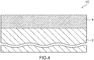
- Fig. 1 shows a schematic sectional view of a surface-treated material of a first embodiment.
- the illustrated surface-treated material 1 has a conductive substrate 2 and a surface treatment film 4, and further has the zinc-containing layer 3 formed between the conductive substrate 2 and the surface treatment film 4.
- the conductive substrate 2 is not limited in particular, but is preferably mainly formed of any of base metals having, for instance, a large ionization tendency, and among them, for instance, aluminum (Al) or an aluminum alloy which is difficult to have a sound plating film formed thereon with the use of a wet plating method, in a point that the conductive substrate can remarkably exhibit an effect of the present invention.
- the shape of the conductive substrate 2 is illustrated by an example of a strip, but may be a form of a plate, a wire, a rod, a pipe, a foil or the like, and various shapes can be adopted according to the application.
- the surface treatment film 4 is formed on the conductive substrate 2, and includes at least one layer of metal layers.
- Each of the metal layers forming the surface treatment film 4 can be formed of a metal or an alloy which is appropriately selected from among, for instance, nickel (Ni), a nickel alloy, cobalt (Co), a cobalt alloy, copper (Cu), a copper alloy, tin (Sn), a tin alloy, silver (Ag), a silver alloy, gold (Au), a gold alloy, platinum (Pt), a platinum alloy, rhodium (Rh), a rhodium alloy, ruthenium (Ru), a ruthenium alloy, iridium (Ir), an iridium alloy, palladium (Pd), a palladium alloy, according to purposes of imparting desired characteristics.
- a surface-treated material (plated material) excellent in long-term reliability can be obtained by: forming one or more metal layers as an intermediate layer, which are formed of a metal or an alloy selected from nickel, a nickel alloy, cobalt, a cobalt alloy, copper, a copper alloy, silver and a silver alloy, on the conductive substrate 2 that has been subjected at least to a first surface activation treatment step which will be described later; and then, forming a single layer or a plurality of metal layers on the intermediate layer, which are formed of a metal or an alloy selected from tin, a tin alloy, silver, a silver alloy, gold, a gold alloy, platinum, a platinum alloy, rhodium, a rhodium alloy, ruthenium, a ruthenium alloy, iridium, an iridium alloy, palladium and a palladium alloy, as a covering layer for impart
- the number of metal layers forming the surface treatment film 4 is not limited in particular, and can be appropriately selected as needed.
- the surface treatment film 4 preferably includes two or more metal layers that include: at least a metal layer formed for the purpose of improving the adhesiveness to the substrate, and the like, as an intermediate layer (underlying layer); and a metal layer for imparting functions, as a covering layer.
- the surface treatment film 4 is a wet plating film.
- the characteristic constitution of the present invention exists in simply forming the surface treatment film 4 having the adequate adhesiveness to the conductive substrate 2, and more specifically, exists in that the surface treatment film 4 is a wet plating film, is formed on the whole surface or a part of the conductive substrate 2 through a zinc-containing layer 3 which contains zinc as a main component and has a thickness of 50 nm or less, or is formed on the conductive substrate without through the zinc-containing layer, and has a ratio of a contact area to a test area of 85% or more, which is measured according to a tape test method defined in JIS H 8504: 1999.
- the surface treatment film 4 can inhibit the deterioration of characteristics on the surface of the surface treatment film, in particular, the adhesiveness, contact resistance and solder wettability in high-temperature (for instance, 200°C) use environment, without deteriorating moldability such as bending workability, in comparison with a conventional surface-treated material in which a zinc-containing layer (particularly, zincate treatment layer) having a thickness, for instance, of approximately 100 nm is interposed between the substrate 2 and the surface treatment film 4 that is a plating film.
- a zinc-containing layer particularly, zincate treatment layer
- the conductive substrate 2 in particular, the conductive substrate 2 that is a base metal having a large ionization tendency, such as aluminum or an aluminum alloy, is subjected to substitution treatment by zinc as a usual method, which is so-called zincate treatment.
- the thickness of the zinc-containing layer which exists between the substrate and the surface treatment film is, for instance, approximately 100 nm; when zinc in the zinc-containing layer is diffused in the surface treatment film and is further diffused up to and appears on the surface layer of the surface treatment film, when, for instance, the surface-treated material is used as an electric point, the zinc causes a problem of resulting in increasing a contact resistance, and further various problems of lowering wire bonding properties, lowering solder wettability and lowering corrosion resistance; and as a result, there has been a case in which the characteristics of the surface-treated material deteriorate due to use, and the long-term reliability is impaired.
- the thickness of the nickel-based plating layer is controlled to be excessively thick in order to inhibit the diffusion of zinc, when a bending work has been applied in a step of producing a terminal, the nickel-based plating layer (film) cannot follow the deformation of the aluminum-based substrate, cracks easily occur, and corrosion resistance is also inferior.
- the nickel-based plating layer is thinly formed, it is difficult to completely cover the zinc-containing layer due to the formation of a non-uniform plating layer and the formation of pinholes, and there has been a problem that erosion preferentially proceeds along the zinc-containing layer in the salt water environment, and that peeling consequently occurs between the nickel-based plating layer and the substrate.
- the zinc-containing layer not to exist between the substrate 2 and the surface treatment film 4, but in the conventional film forming technique, unless the zinc-containing layer (in particular, zincate treatment layer) exists, it has been considered difficult to form a surface treatment film (plating film) having adequate adhesiveness to the conductive substrate 2, in particular, the conductive substrate 2 which is a base metal having a large ionization tendency.
- the present inventors made an extensive investigation, and found that: by subjecting a surface of the conductive substrate 2 (for instance, aluminum substrate) to a new first surface activation treatment step, prior to the formation of the surface treatment film (plating film) 4, it is possible to effectively remove the oxide film which stably exists on the surface of the conductive substrate 2, even without forming a conventional zinc-containing layer (in particular, zincate treatment layer), and accordingly even though the surface treatment film (for instance, nickel plating layer) is directly formed on the conductive substrate, metal atoms (for instance, nickel atoms) forming the surface treatment film can directly bond to metal atoms (for instance, aluminum atoms) forming the conductive substrate without through oxygen atoms; and as a result, it is possible to simply form the surface treatment film 4 having the adequate adhesiveness on the conductive substrate 2.
- the reason why a ratio of a contact area to a test area has been determined to be 85% or more as measured according to a tape test method defined in JIS H 8504:1999, is because when the contact area is less than 85%, not only the adhesiveness is inferior in comparison with that of the conventional surface-treated material on which the zinc-containing layer (in particular, zincate treatment layer) is formed, but also the advantage of the adhesiveness becomes unremarkable in comparison with the conventional surface-treated material formed using other plating methods other than the zinc zincate treatment method, and deterioration in the adhesiveness, the contact resistance and the solder wettability in high-temperature (for instance, 200°C) use environment cannot be also sufficiently inhibited.
- most of the oxide film which exists on the surface of the conductive substrate 2 can be removed by conducting the first surface activation treatment step, but even if a part of the oxide film partially remains on the surface of the conductive substrate 2, such a degree does not aggregate the adhesiveness so much, and accordingly such a case is also included within the scope of the present invention.
- the surface-treated material is "formed on the conductive substrate without through the zinc-containing layer", in the case where when in a cross-sectional observation of the surface-treated material, portions between a portion of the conductive substrate and a portion of the surface treatment film are subjected to a line analysis with the use of STEM-EDX, and when an obtained profile of detection intensity of each component of the surface-treated material is viewed, the maximum value of an intensity ratio of zinc to a main component of the surface treatment film is 1/4 or less, in a specific analysis range in which the intensity of the main component of the surface treatment film is equal to or higher than the intensity of the main component of the conductive substrate.
- the surface-treated material is formed on the conductive substrate without through the zinc-containing layer, in the case where the number is 0, which is obtained by the processes of: determining five points aligned on a straight line at intervals of 50 ⁇ m in two different positions, at arbitrary points of the conductive substrate, for instance, in the cross-sectional observation of the surface-treated material; subjecting each of the ten points to FIB processing; then subjecting an area of 100 nm ⁇ 100 nm to the surface analysis with the use of STEM-EDX and with a resolution of 1 nm/pixel or more so that the interface between the conductive substrate and the surface treatment film comes to the vicinity of the center (see Fig. 5(a) and Fig.
- the present inventors found also that even in the case where the surface of the conductive substrate is subjected to a second surface activation treatment step which uses a zinc substitution method, prior to conducting a first surface activation treatment step, a thin zinc-containing layer having a thickness of 50 nm or less is formed on the whole surface or a part of the conductive substrate, and the surface treatment film is indirectly formed through the zinc-containing layer, zinc in the zinc-containing layer is inhibited from being diffused to the outermost surface of the surface covering layer by the first surface activation treatment step conducted after that, because an absolute amount of zinc which exists on the surface of the conductive substrate 2 is small in comparison with that in the conventional surface-treated material in which a thick (for instance, approximately 100 nm) zinc-containing layer exists, and also the surface treatment film 4 having the adequate adhesiveness can be simply formed on the conductive substrate 2.
- the zinc-containing layer 3 can be formed between the conductive substrate 2 and the surface treatment film 4, as needed.
- the thickness of the zinc-containing layer 3 is controlled preferably to be 50 nm or less, more preferably to be 30 nm or less, and further preferably to be 1 nm or more and 15 nm or less.
- the thickness of the zinc-containing layer 3 is formed so as to be more than 50 nm, the absolute amount of zinc increases which exists on the surface of the conductive substrate 2, accordingly zinc diffuses in the surface treatment film 4, the zinc reaches the outermost surface layer of the surface treatment film 4, and thereby becomes easy to form zinc oxide and the like; and thereby an increase in contact resistance and deterioration in solder wettability become easy to occur during use, and long-term reliability is impaired.
- the zinc-containing layer 3 does not exist between the conductive substrate 2 and the surface treatment film 4, and even though the zinc-containing layer 3 exists, it is most preferable that the layer is thinner than 1 nm.
- the zinc-containing layer 3 is a layer which contains zinc as a main component, specifically, is a layer which contains 50 to 100% by mass of zinc.
- Specific examples of the zinc-containing layer 3 include a zinc layer which is formed by a zinc substitution treatment (zincate treatment), and a zinc alloy layer such as a zinc-copper alloy and a zinc-iron alloy.
- Figs 1 to 4 show several embodiments of the present invention.
- Fig. 1 shows a case in which the zinc-containing layer 3 is formed between the conductive substrate 2 and the surface treatment film 4, uniformly over the whole surface of the conductive substrate 2.
- both of Fig. 2 and Fig. 3 show a case in which the zinc-containing layer 3 is partially formed on the surface of the conductive substrate 2, and the surface of the conductive substrate 2 is not completely covered;
- Fig. 2 shows a case in which an existence ratio of the zinc-containing layer 3 covering the surface of the conductive substrate 2 is controlled to be large;
- Fig. 3 shows a case in which an existence ratio of the zinc-containing layer 3 covering the surface of the conductive substrate 2 is controlled to be small, and the zinc-containing layer 3 is formed in an island-shaped pattern.
- the thickness of the zinc-containing layer 3 in the case in which the zinc-containing layer 3 is partially formed on the surface of the conductive substrate 2 shall be a thickness that is measured in a portion corresponding to the zinc-containing layer which exists partially on the surface of the conductive substrate 2; and in the present invention, it is necessary to adjust the thickness of the portion corresponding to the zinc-containing layer to 50 nm or less.
- Fig. 4 shows a case in which the zinc-containing layer 3 does not exist between the conductive substrate 2 and the surface treatment film 4, and the surface treatment film 4 is directly formed on the conductive substrate 2.
- the thickness of the zinc-containing layer 3 was measured by: measuring arbitrary five points in a collimator diameter of 200 ⁇ m with a fluorescent X-ray measuring apparatus (for instance, SFT 9400: Hitachi High-Technologies Corporation (made by former Seiko Instruments Inc.); and calculating an average value thereof.
- a fluorescent X-ray measuring apparatus for instance, SFT 9400: Hitachi High-Technologies Corporation (made by former Seiko Instruments Inc.); and calculating an average value thereof.
- FIB Fluorused Ion Beam
- a plate material, a rod material or a wire material that is a substrate of aluminum for instance, 1000 series of aluminum such as A1100 which is defined in JIS H 4000: 2014, and an aluminum alloy (for instance, 6000(Al-Mg-Si) series alloy such as A6061 which is defined in JIS H 4000: 2014), to an electrolytic degreasing step, a first surface activation treatment step and a surface treatment film forming step, or an electrolytic degreasing step, a second surface activation treatment step (zinc-containing thick film layer forming and removing step), a first surface activation treatment step and a surface treatment film forming step; and in addition, in order to produce a surface-treated material having a cross-sectional layer structure shown in Figs 1 to 3 , for instance, it is acceptable to sequentially subject the substrate to an electrolytic degrea
- the electrolytic degreasing step includes a method of immersing the substrate in an alkaline degreasing bath of, for instance, 40 to 100 g/L sodium hydroxide (NaOH), setting the above described substrate as a cathode, and subjecting the substrate to cathodic degreasing under conditions of a current density of 2.5 to 5.0 A/dm 2 , a bath temperature of 60°C and a treatment time period of 10-60 seconds.
- an alkaline degreasing bath of, for instance, 40 to 100 g/L sodium hydroxide (NaOH)
- the second surface activation treatment step is a step which is conducted by using a zinc substitution method (zincate treatment), and in the case where the surface-treated material having the cross-sectional layer structure is produced in which the zinc-containing layer does not exist as is shown in Fig. 4 , the step can be omitted.
- the second surface activation treatment step may be conducted, but in this case, the second surface activation treatment step is a step of forming the zinc-containing thick film layer and removing the zinc-containing thick film layer by the dissolution.
- the second surface activation treatment step is a step of forming the zinc-containing layer by forming the zinc-containing thick film layer and partially dissolving the thick layer, and in this case, the step becomes an essential step.
- the zinc-containing thick film layer can be formed on the basis of the zinc substitution bath composition and treatment conditions, for instance, shown in Table 1.
- Table 1 Zinc substitution treatment Zinc substitution bath composition
- Treatment conditions Com ponent Concentration (g/L) NaOH 500 Immersion treatment ZnO 100 Bath temperature: room temperature Tartaric acid (C 4 H 6 O 6 ) 10 Treatment time period: 1 to 300 seconds FeCl 2 2
- the second surface activation treatment step it is preferable, for instance, to temporarily form the zinc-containing thick film layer having a thickness of 100 nm or more on the surface of the conductive substrate by a zinc substitution method, then to dissolve the above described zinc-containing thick film layer in a range of 50 nm or more, and thereby to reduce the thickness thereof to a range of 50 nm or less to form the above described zinc-containing layer, or to completely remove the zinc-containing thick film layer.
- a thin zinc-containing layer of 50 nm or less not by forming the zinc-containing thick film layer of 100 nm or more and then dissolving the zinc-containing layer to form a zinc-containing layer as in the second surface activation treatment step of the present invention, but by simply conducting the zinc substitution treatment for a short time; however, the method is not preferable because when the treatment time period is short, the peeling of the surface treatment film (plating film) which is formed thereafter becomes easy to occur.
- the upper limit of the thickness of the zinc-containing thick film layer is not limited in particular, but is preferably set at 200 nm or less, because even if the thickness is set as to be thicker than 200 nm, the amount of zinc at the time of being dissolved wastefully increases, and only the cost increases and the treatment time period becomes long.
- the zinc-containing thick film layer can be dissolved by immersing the above described substrate which has been electrolytically degreased, for instance, in an acid solution of 10 to 30% sulfuric acid; and adjusting an immersion time period.
- an immersion time period For instance, when the thickness of the zinc-containing thick film layer having a thickness of 100 nm is decreased to the thickness of 50 nm or less and thereby the zinc-containing layer is formed, it is preferable to set the immersion time period at 20 seconds or longer and shorter than 40 seconds; when the thickness is decreased to the thickness of 30 nm or less, to set at 40 seconds or longer and shorter than 50 seconds; and when the thickness is decreased to the thickness of 15 nm or less, to set at 50 seconds or longer and shorter than 60 seconds.
- the immersion time period 60 seconds or longer.
- these conditions need to be appropriately adjusted according to the conditions of the plating bath and the substrate.
- the second surface activation treatment step is not limited to a method of forming the zinc-containing thick film layer with the use of the zinc substitution method and then controlling the thickness thereof to 50 nm or less by partially dissolving the zinc-containing layer, as has been described above, but can be achieved, for instance, by various methods such as a method of mechanically polishing and removing the zinc-containing thick film layer after zincate treatment, and a method of directly forming the plating by a dry process such as vapor deposition and sputtering, as other methods.
- the first surface activation treatment step is a new activation treatment step different from a conventional activation treatment, and is the most important step in the steps for producing the surface-treated material of the present invention.
- the oxide film which stably exists on the surface of the conductive substrate 2 can be effectively removed by conducting the first surface activation treatment step, even if the zinc-containing layer which contains zinc as a main component is not formed by zincate treatment or the like, and even if the surface treatment film (for instance, nickel plating layer) is formed directly on the conductive substrate, metal atoms (for instance, aluminum atoms) forming the conductive substrate and metal atoms (for instance, nickel atoms) forming the surface treatment film can directly bond to each other without through the oxygen atoms; and as a result, the surface treatment film 4 having the adequate adhesiveness can be simply formed on the conductive substrate 2.
- the first surface activation treatment step it is preferable to treat the surface of the conductive substrate 2 by using an activation treatment liquid that contains 10 to 500 ml/L of any one acid solution which is selected from among sulfuric acid, nitric acid, hydrochloric acid, hydrofluoric acid and phosphoric acid, and 0.1 to 500 g/L (in terms of metal content of nickel or cobalt) of nickel compounds which include nickel sulfate, nickel nitrate, nickel chloride and nickel sulfamate, or cobalt compounds which include cobalt sulfate, cobalt nitrate, cobalt chloride and cobalt sulfamate, at a treatment temperature of 20 to 60°C, at a current density of 0.5 to 20 A/dm 2 , and for a treatment time period of 1 to 300 seconds.
- an activation treatment liquid that contains 10 to 500 ml/L of any one acid solution which is selected from among sulfuric acid, nitric acid, hydrochloric acid, hydroflu
- a surface treatment film forming step is conducted.
- the formation of the surface treatment film is formed of at least one metal layer, and each of the metal layers can be formed by electrolytic plating or electroless plating any of which is a wet plating method, according to the purpose of imparting characteristics to the surface-treated material.
- Tables 2 to 11 illustrate plating bath compositions and plating conditions at the time when the metal layer is formed by nickel (Ni) plating, cobalt (Co) plating, copper (Cu)plating, tin (Sn) plating, silver (Ag) plating, silver (Ag)-tin (Sn) alloy plating, silver (Ag)-palladium (Pd) alloy plating, gold (Au) plating, palladium (Pd) plating and rhodium (Rh) plating, respectively.
- the thickness thereof is preferably set in a range of 0.2 ⁇ m or more and 2.0 ⁇ m or less, more preferably of 0.2 ⁇ m or more and 1.5 ⁇ m or less, further preferably of 0.2 ⁇ m or more and 1.0 ⁇ m or less, and most preferably of 0.2 ⁇ m or more and 0.5 ⁇ m or less.
- the nickel plating layer When the thickness of the nickel plating layer is less than 0.2 ⁇ m, the nickel plating layer cannot sufficiently inhibit the diffusion of zinc in the zinc-containing layer having a thickness of 50 nm or less, and contact resistance at 200°C and solder wettability tend to deteriorate; and in addition, when the thickness exceeds 2.0 ⁇ m, the zinc in the zinc-containing layer having a thickness of 50 nm or less resists being diffused, and the deterioration in the contact resistance at 200°C and the solder wettability can be inhibited, but bending workability tends to be inferior.
- the nickel layer can sufficiently inhibit the appearance of the zinc-containing layer on the material surface due to the diffusion of zinc, even when the plating thickness thereof is made thinner than the conventional one, and the contact resistance and the solder wettability do not deteriorate.
- conventionally there has been such a problem that when the nickel layer is thin, the corrosion progresses along the zinc-containing layer in the salt water environment due to the formation of a non-uniform plating film and the formation of pinholes, but it has become possible to make the nickel layer thin by making the zinc-containing layer extremely thin.
- the production method of the present invention can form a plating film excellent in adhesiveness to a conductive substrate by conducting each of the above described steps, and besides, can produce a surface-treated material which can inhibit the deterioration of the adhesiveness, contact resistance and solder wettability, particularly in high-temperature (for instance, 200°C) use environment without deteriorating the bending workability, in comparison with a conventional surface-treated material in which a zinc-containing layer (in particular, zincate treatment layer) having a thickness of approximately 100 nm is interposed, by a simple method.
- a zinc-containing layer in particular, zincate treatment layer
- the surface-treated material of the present invention can use aluminum, an aluminum alloy and the like which have lighter weight, as a substrate (conductive substrate), in place of iron, an iron alloy, copper, a copper alloy or the like which have been conventionally used, and can be applied to various products such as a terminal, a connector, a bus bar, a lead frame, a medical member (for instance, guide wire for catheter, stent, artificial joint and the like), a shield case (for instance, for preventing electromagnetic waves), a coil (for instance, for motor), an accessory (for instance, necklace, earring, ring and the like), and a contact switch.
- the surface-treated material has been formed so as to be capable of withstanding the same use environment as that of a conventional product group formed of iron, an iron alloy, copper and a copper alloy, by making it possible to activate the surface of the substrate without making a conventional thick zinc-containing layer (in particular, zincate treatment layer) of approximately 100 nm exist between the substrate and the surface treatment film; and can be used in various products such as wire harness for automotive applications and housing for aerospace applications, which are particularly required to reduce the weight.
- a conventional thick zinc-containing layer in particular, zincate treatment layer
- An electric degreasing step was conducted on aluminum-based substrates (size of 0.2 mm ⁇ 30 mm ⁇ 30 mm) shown in Table 12, under the above described conditions; then, as for Inventive Examples 1 to 4, 6 to 11 and 15 to 20, the zincate treatment was carried out which formed the above described second surface activation treatment, according to the zinc substitution treatment condition shown in Table 1; thereby the zinc-containing thick film layers were formed so as to have thicknesses shown in Table 12, and were partially dissolved, respectively; and the zinc-containing layers are formed so as to have thicknesses shown in Table 12, respectively.
- Inventive Examples 5, 12 to 14 and 21 are not subjected to the second surface activation treatment (zinc-containing layer is not formed).
- the first surface activation treatment was conducted with the use of an activation treatment liquid which contained 10 to 500 ml/L of an acid solution including sulfuric acid, nitric acid, hydrochloric acid, hydrofluoric acid and phosphoric acid, and 0.1 to 500 g/L (in terms of metal content of nickel) of nickel compounds including nickel sulfate, nickel chloride and nickel nitrate, under conditions of a treatment temperature of 20 to 60°C, a current density of 0.5 to 20 A/dm 2 and a treatment time period of 30 seconds.
- an activation treatment liquid which contained 10 to 500 ml/L of an acid solution including sulfuric acid, nitric acid, hydrochloric acid, hydrofluoric acid and phosphoric acid, and 0.1 to 500 g/L (in terms of metal content of nickel) of nickel compounds including nickel sulfate, nickel chloride and nickel nitrate, under conditions of a treatment temperature of 20 to 60°C, a current density of 0.5 to 20 A/dm 2 and
- the first surface activation treatment was conducted with the use of an activation treatment liquid which contained 10 to 500 ml/L of an acid solution including sulfuric acid, nitric acid, hydrochloric acid, hydrofluoric acid and phosphoric acid, and 5 g/L (in terms of metal content of cobalt) of cobalt compounds including cobalt sulfate, cobalt chloride and cobalt nitrate, under conditions of a treatment temperature of 20 to 60°C, a current density of 0.5 to 20 A/dm 2 and a treatment time period of 30 seconds.
- an activation treatment liquid which contained 10 to 500 ml/L of an acid solution including sulfuric acid, nitric acid, hydrochloric acid, hydrofluoric acid and phosphoric acid, and 5 g/L (in terms of metal content of cobalt) of cobalt compounds including cobalt sulfate, cobalt chloride and cobalt nitrate, under conditions of a treatment temperature of 20 to 60°C, a
- surface treatment films were formed which includes two or three metal layers formed with the thicknesses shown in Table 12 by the above described surface treatment film forming step, respectively, and the surface-treated materials were prepared. Incidentally, the formation conditions of each of the metal layers forming the surface treatment film were conducted under the plating conditions shown in Tables 2 to 11.
- Comparative Example 1 a surface-treated material was produced on the same conditions as in Inventive Example 1 except that the thickness of the zinc-containing layer was as thick as 55 nm, and was prepared.
- the line analysis was conducted in a range of 70 nm or more from the conductive substrate side to the surface treatment film side, and in thus obtained profile of detection intensity of each component of the surface-treated material, the number of times when the maximum value of the intensity ratio of the zinc to the main component of the surface treatment film exceeds 1/4, in such a range that the intensity of the main component of the surface treatment film became equal to or higher than the intensity of the main component of the conductive substrate; and the result is shown in Table 12.
- the plating adhesiveness was evaluated as "excellent” when the peeling of the plating was not observed and the ratio of the contact area to the test area was 100%, was evaluated as “good” when the ratio was 95% or more and less than 100%, was evaluated as “fair” when the ratio was 85% or more and less than 95%, was evaluated as “poor” when the ratio was 70% or more and less than 85%, and was evaluated as "unacceptable” when the ratio was less than 70%; and in the present example, "excellent", "good” and "fair” were evaluated as acceptable.
- the contact resistance shown in Table 14 was evaluated as “excellent” when the contact resistance was 10 m ⁇ or less, was evaluated as “good” when the contact resistance exceeded 10 m ⁇ and was 50 m ⁇ or less, was evaluated as “fair” when the contact resistance exceeded 50 m ⁇ and was 100 m ⁇ or less, and was evaluated as “poor” when the contact resistance exceeded 100 m ⁇ ; and in the present example, “excellent", "good” and “fair” were evaluated as acceptable.
- solder wettability two types of samples were prepared for every prepared surface-treated material, which were in such a state that the surface treatment film was just formed (as plated) and in such a state that the surface treatment film was subjected to heat treatment at 200°C in the atmosphere for 24 hours, and solder wetting time periods were evaluated with the use of a solder checker (SAT-5100 (trade name, made by RESCA, Inc.)). Table 14 shows the evaluation results.
- solder wettability shown in Table 14 was measured under measurement conditions of which the details are as follows, and was evaluated as “excellent” when the solder wetting time period was shorter than 3 seconds, was evaluated as “good” when the solder wetting time period was 3 seconds or longer and shorter than 5 seconds, was evaluated as “fair” when the solder wetting time period was 5 seconds or longer and shorter than 10 seconds and was evaluated as “poor” when the surface treatment material was immersed for 10 seconds but was not bonded; and in the present example, “excellent”, “good”, and “fair” were evaluated as acceptable.
- the first surface activation treatment step was not conducted, and besides, a zinc-containing layer as thick as 110 nm was formed by the conventional zincate treatment; and accordingly the contact resistance and the solder wettability at 200°C were inferior.
- the nickel plating layer which was an underlying layer was thickly formed in comparison with that of Conventional Example 1, and accordingly the deterioration in the contact resistance and the solder wettability at 200°C are inhibited, but the bending workability is inferior.
- both of the first surface activation treatment step and the conventional zincate treatment were not conducted, and accordingly the adhesiveness and the bending workability were inferior, and the contact resistance and the solder wettability at 200°C were also inferior.
- Conventional Example 4 was not subjected to the first surface activation treatment but was treated with the conventional nickel plating liquid containing the hydrofluoric acid and the nickel salt, accordingly the adhesiveness was inferior, and the adhesiveness, the contact resistance and the solder wettability at 200°C were also inferior.
- the thickness of the zinc-containing layer formed in the second surface activation treatment step was as thick as 55 nm, and accordingly the contact resistance and solder wettability at 200°C were inferior.
- a surface-treated material that can inhibit deterioration in characteristics on the surface of the surface treatment film, in particular, deterioration in the adhesiveness, contact resistance and solder wettability in high-temperature (for instance, 200°C) use environment, without deterioration in bending workability, in comparison with a conventional surface-treated material in which a zinc layer (zincate treatment layer) having a thickness, for instance, of approximately 100 nm between the conductive substrate and the plating film; and as a result, has high long-term reliability while keeping characteristics after the surface treatment film has been formed: a method for producing the surface-treated material: and various components that are formed by using the surface-treated material.
Landscapes
- Chemical & Material Sciences (AREA)
- Metallurgy (AREA)
- Chemical Kinetics & Catalysis (AREA)
- Engineering & Computer Science (AREA)
- Materials Engineering (AREA)
- Organic Chemistry (AREA)
- Mechanical Engineering (AREA)
- General Chemical & Material Sciences (AREA)
- Electrochemistry (AREA)
- Electroplating Methods And Accessories (AREA)
- Other Surface Treatments For Metallic Materials (AREA)
- Chemically Coating (AREA)
- Laminated Bodies (AREA)
Abstract
Description
- The present invention relates to a surface-treated material, a method for producing the surface-treated material, and a component formed by using the surface-treated material, and particularly relates to a technology that simply forms a surface treatment film which includes at least one layer of metal layers and has an adequate adhesiveness, on an conductive substrate which is mainly formed of a base metal having a large ionization tendency and is considered to be difficult to form a sound plating film thereon.
- For a material to be plated (conductive substrate) which is used for forming a conventional electrical contact and the like, metal materials such as copper, copper alloys, iron and iron alloys have been widely used, from the viewpoint of being inexpensive and having comparatively excellent characteristics. Since such metal materials are satisfactory particularly in conductivity and workability, are comparatively easily available, in addition, is easily to apply coating treatment on its surface, and have a surface excellent in plating adhesiveness, the metal materials are still used as mainstream materials for the conductive substrate.
- However, copper (specific gravity of 8.96) and iron (specific gravity of 7.87) are materials each having a comparatively high specific gravity, and accordingly, for instance, in a wire harness for automobiles and bodywork of an aircraft, materials such as aluminum (specific gravity of 2.70) and magnesium (specific gravity of 1.74) each having a comparatively low specific gravity have been increasingly used in recent years in place of copper and iron.
- By the way, it is considered that a method of plating the surface of the aluminum which is referred to as a light metal among metals is complicated, and besides that it is difficult for aluminum to form a plating film with adequate adhesiveness thereon. There are such factors of causing the above phenomenon that aluminum is apt to form an oxide film called a passivation film on its surface, this oxide film exists in a stable state, and it is difficult for a base metal such as aluminum to be plated in a wet process.
- In order to inhibit the formation of an oxide film on the surface of the aluminum-based substrate, conventionally, such measures have been taken as to cover the surface of the substrate with a metal such as tin, and keep the contact resistance or inhibit the increase thereof (for instance,
Patent Literature 1 and the like). - In addition, in the case where an underlying layer such as a nickel layer which is formed for the purpose of improving plating adhesiveness and a covering layer which is formed of a metal (tin, silver and the like) for electric contact are sequentially formed on the surface of an aluminum-based substrate , for instance, by a wet plating method, even if the underlying layer is formed on the surface of the substrate and then the covering layer is formed on the underlying layer, sufficient adhesiveness cannot be usually obtained due to an oxide film present on the surface of the substrate.
- Thus, conventionally, a pre-treatment has been carried out for enhancing an adhesive strength between the substrate and the plating film (underlying layer and covering layer), by conducting zinc substitution treatment which is referred to as zincate treatment, with the use of a solution containing zinc, before forming the underlying layer and the covering layer (for instance, Patent Literature 2).
- In
Patent Literature 3, an electronic component material is described which is a plated aluminum alloy, and it has been considered to be preferable that a certain amount or more of a zinc layer exists for providing a sufficient bonding force. It is described that the substrate may be plated without forming the zinc layer thereon, but the production method is not clearly stated. Accordingly, the effect is not examined which is obtained when the zinc layer is reduced to the extreme or when the zinc layer is not formed. - In addition, in
Patent Literature 4, such a method is described as to perform a pre-treatment for forming fine etched recesses on the surface of the substrate by etching with an active acid treatment liquid, and enhance an adhesive strength by an anchor effect due to the formed fine etching recesses. However, there has been a problem that bending workability deteriorates because the unevenness of 5 to 10 µm becomes a stress concentration point at the time of deformation. - Generally, in a plating film which has been formed after the zincate treatment is performed on the surface of the aluminum substrate , the zinc layer which has been formed to have a thickness of, for instance, approximately 100 nm is interposed between the substrate and the plating film, and the plating layer (plating film) is formed on this zinc layer; and accordingly when heated, zinc in the zinc layer is consequently diffused in the plating layer and is further diffused up to and appears on the surface layer of the plating layer. As a result, such various problems arise that a contact resistance results in increasing, wire bonding properties are lowered and solder wettability is lowered. In motors of trains and electric locomotives, in particular, it has been studied to change metal of winding wires to aluminum so as to reduce the weight, but the wire reaches 160°C depending on the portion, and accordingly it is necessary to improve the heat resistance of a plating film which has been formed on the surface of the conductor. A large-sized bus bar and the like show a great effect of reduction in weight due to the change to aluminum. These are produced by welding several components, but the temperature in the vicinity of the welded portion becomes high, and accordingly a plating film having a higher heat resistance is required.
- In addition, in recent years, sudden heavy rain has increased, and when struck by lightning, a large current instantaneously flows, and heat which is generated by Joule heat at the time is said to be 180°C or higher. Heat resistance is necessary for a conductor which is used in a power distribution board and the like. Furthermore, aluminum has been progressively used for a wire harness of automobiles, and a heat resistance of 150°C is required in the periphery of an engine and the periphery of a high power motor. From such a background in recent years, the plating is required which does not cause deterioration in adhesiveness and an increase in contact resistance even when being held at 200°C for 24 hours in an accelerated test.
- Furthermore, in some states of the zinc layer formed in the zincate treatment, there have been cases where plating defects often occur such as the formation of bumps in the subsequent plating and precipitation abnormality.
- Still furthermore, in a drone and a wearable device, there is a possibility that rain and sweat get inside the device, and high corrosion resistance is required also in order that long-term reliability is ensured. The same applies to motors and inverters of an electric transformer in a salt water environment such as wind-power generation. However, if the plating layer (underlying layer) which is formed after the zinc substitution treatment is thinly formed, it is difficult to completely cover the zinc-containing layer due to the formation of a non-uniform plating layer and the formation of pinholes, and there is a problem that erosion preferentially proceeds along the zinc-containing layer in the salt water environment, and that as a result, peeling occurs between the underlying layer and the substrate.
- Thus, in order that the above described problem does not occur, it is desirable not to allow the zinc layer to exist between the substrate and the plating film, and when it is necessary to form the zinc layer, it is desirable to form a zinc layer having a thickness as thin as possible.
- As for a method of plating a substrate of aluminum without through the zinc layer, for instance, in Patent Literature 5, it is described that aluminum or an aluminum alloy can be electroless nickel plated by using a nickel plating liquid which contains a hydrofluoric acid and/or a salt thereof, a nickel salt and water. However, in the electroless nickel plating, nickel precipitated disorderly, mismatch among lattices became large, and accordingly sufficient adhesiveness could not be obtained.
- In addition, it is general to use a nickel-based plating layer as the underlying layer, and the nickel-based plating layer is formed mainly with the intention of enhancing the adhesiveness and inhibiting the diffusion of zinc in the zinc layer. However, the nickel-based plating layer is usually harder than the aluminum-based substrate, and accordingly there are problems that if the thickness of the nickel-based plating layer is formed excessively thick in order to inhibit the diffusion of zinc, the nickel-based plating layer (film) cannot follow the deformation of the aluminum-based substrate, when a bending work has been applied to the plating layer in a step of producing a terminal, cracks easily occur, and corrosion resistance is also inferior.
- Furthermore, in recent years, the miniaturization of electronic components and the like has progressed, and bendability under severer conditions is required. For instance, when aluminum is used in bus bars and electric wires, it is necessary to increase the cross-sectional area so as to match the resistances of the conductors. When the conductors are subjected to a bending work which does not change the inner bending radius, the conductor having a larger cross-sectional area results in showing a larger tensile strain on the outer side of the bent part, and tends to easily cause cracks on the plating surface.
- In addition, also in the field where aluminum has already been used, for instance, in the bus bar for automobiles, miniaturization is required; and it is required that cracks do not occur in the plating, even if the bus bar has been subjected to working such as bending, twisting and shearing which are under severer conditions than before. Furthermore, also in the latest applications such as drones and wearables in which light weight is required, it is being studied to change the material to aluminum from copper and steel, but even if the components are subjected to severe working in order to be miniaturized, it is required that cracks do not occur on the plating surface. In these applications, such problems have also arisen that cracks result in occurring when the nickel-based plating which has been used for inhibiting the diffusion of zinc has a conventional thickness.
-
- Patent Document 1: Japanese Laid-Open Patent Publication No.
2014-63662 -
Patent Document 2 Japanese Laid-Open Patent Publication No.2014-47360 - Patent Document 3: Japanese Laid-Open Patent Publication No.
2012-087411 - Patent Document 4: Japanese Laid-Open Patent Publication No.
2002-115086 - Patent Document 5: Japanese Laid-Open Patent Publication No.
2011-99161 - Then, an object of the present invention is to provide a surface-treated material that can have a surface treatment film having adequate adhesiveness simply formed on a conductive substrate which is mainly formed of a base metal particularly having a large ionization tendency such as aluminum and an aluminum alloy, and is considered to be difficult to form a sound plating film thereon, and besides that inhibits the deterioration of characteristics on the surface of the surface treatment film, which are adhesiveness, contact resistance and solder wettability particularly in high-temperature (for instance, 200°C) use environment, in comparison with a conventional surface-treated material in which a zinc layer (in particular, zincate treatment layer) having a thickness, for instance, of approximately 100 nm is interposed between the substrate and the plating film, without deteriorating moldability such as bending workability; a method for producing the surface-treated material; and a component that is formed by using the surface-treated material.
- The present inventors have made an extensive investigation on the above described problem, and as a result; have found that a surface-treated material which exhibits excellent plating adhesiveness and adequate characteristics after plating can be provided by forming a surface treatment film on an conductive substrate which is mainly formed of a base metal in an appropriately multilayered state; and thereby have reached the present invention.
- Specifically, the summary and the constitution of the present invention are as follows.
- (1) A surface-treated material has a conductive substrate, and a surface treatment film which includes at least one layer of metal layers and is formed on the conductive substrate, wherein the surface treatment film is a wet plating film; is formed on a whole surface or a part of the conductive substrate through a zinc-containing layer that contains zinc as a main component and has a thickness of 50 nm or less, or is formed on the conductive substrate without through the zinc-containing layer; and a ratio of a contact area to a test area is 85% or more as measured according to a tape test method defined in JIS H 8504: 1999.
- (2) A surface-treated material has a conductive substrate, and a surface treatment film which includes at least one layer of metal layers and is formed on the conductive substrate, wherein in cross-sectional observation of the surface-treated material, when portions between a portion of the conductive substrate and a portion of the surface treatment film are subjected to a line analysis with the use of STEM-EDX, and an obtained profile of detection intensity of each component of the surface-treated material is viewed, a maximum value of an intensity ratio of zinc to a main component of the surface treatment film is 1/4 or less, in a specific analysis range in which the intensity of the main component of the surface treatment film is equal to or higher than the intensity of the main component of the conductive substrate; and a ratio of a contact area to a test area is 85% or more as measured according to a tape test method defined in JIS H 8504: 1999.
- (3) The surface-treated material according to the above described (1) or (2), wherein the conductive substrate is aluminum or an aluminum alloy.
- (4) The surface-treated material according to any one of the above described (1) to (3), wherein each of the metal layers forming the surface treatment film is formed of any one selected from the group consisting of nickel, a nickel alloy, cobalt, a cobalt alloy, copper, a copper alloy, tin, a tin alloy, silver, a silver alloy, gold, a gold alloy, platinum, a platinum alloy, rhodium, a rhodium alloy, ruthenium, a ruthenium alloy, iridium, an iridium alloy, palladium, and a palladium alloy.
- (5) The surface-treated material according to any one of the above described (1) to (4), wherein the surface treatment film includes two or more metal layers.
- (6) A method for producing a surface-treated material according to any one of the above described (1) to (5) includes: a first surface activation treatment step of treating a surface of the conductive substrate, with the use of an activation treatment liquid that contains 10 to 500 mL/L of any one acid solution which is selected from among sulfuric acid, nitric acid, hydrochloric acid, hydrofluoric acid and phosphoric acid, and 0.1 to 500 g/L (in terms of metal content of nickel or cobalt) of nickel compounds which include nickel sulfate, nickel nitrate, nickel chloride and nickel sulfamate, or cobalt compounds which include cobalt sulfate, cobalt nitrate, cobalt chloride and cobalt sulfamate, at a treatment temperature of 20 to 60°C, at a current density of 0.5 to 20 A/dm2, and for a treatment time period of 1 to 300 seconds, prior to forming the surface treatment film on the conductive substrate by a wet plating method.
- (7) The method for producing the surface-treated material according to the above described (6) further includes: a second surface activation treatment step of temporarily forming a zinc-containing thick film layer having a thickness of 100 nm or more on the surface of the conductive substrate by a zinc substitution method, then dissolving the zinc-containing thick film layer in a range of 50 nm or more, and thereby reducing the thickness to a range of 50 nm or less to form the zinc-containing layer, or completely removing the zinc-containing thick film layer, prior to performing the first surface activation treatment step.
- (8) A terminal formed with the use of the surface-treated material according to any one of the above described (1) to (5).
- (9) A connector formed with the use of the surface-treated material according to any one of the above described (1) to (5).
- (10) A bus bar formed with the use of the surface-treated material according to any one of the above described (1) to (5).
- (11) A lead frame formed with the use of the surface-treated material according to any one of the above described (1) to (5).
- (12) A medical member formed with the use of the surface-treated material according to any one of the above described (1) to (5).
- (13) A shield case formed with the use of the surface-treated material according to any one of the above described (1) to (5).
- (14) A coil formed with the use of the surface-treated material according to any one of the above described (1) to (5).
- (15) A contact switch formed with the use of the surface-treated material according to any one of the above described (1) to (5).
- According to the present invention, there can be provided a surface-treated material that has a conductive substrate, in particular, a conductive substrate which is, for instance, aluminum or an aluminum alloy which is mainly formed of a base metal having a large ionization tendency and is considered to be difficult to form a sound plating film thereon, and a surface treatment film which includes at least one layer of metal layers and which is formed on the conductive substrate; by that the surface treatment film is a wet plating film, is formed on the whole surface or a part of the conductive substrate through a zinc-containing layer which contains zinc as a main component and has a thickness of 50 nm or less, or is formed on the conductive substrate without through the zinc-containing layer, and a ratio of a contact area to a test area is 85% or more as measured according to a tape test method defined in JIS H 8504: 1999, can inhibit deterioration in characteristics on the surface of the surface treatment film, in particular, deterioration in adhesiveness, contact resistance and solder wettability in high-temperature (for instance, 200°C) use environment, without deterioration in bending workability, in comparison with a conventional surface-treated material in which a zinc-containing layer (in particular, zincate treatment layer) having a thickness, for instance, of approximately 100 nm between the substrate and the plating film; and as a result, has high long-term reliability while keeping characteristics after the surface treatment film has been formed: a method for producing the same: and various components that are formed by using the surface-treated material.
-
-
Fig. 1 is a schematic sectional view of a surface-treated material which is a first embodiment according to the present invention. -
Fig. 2 is a schematic sectional view of a surface-treated material which is a second embodiment. -
Fig. 3 is a schematic sectional view of a surface-treated material which is a third embodiment. -
Fig. 4 is a schematic sectional view of a surface-treated material which is a fourth embodiment. -
Fig. 5 is a view for describing a method of conducting a line analysis on portions between a portion of a conductive substrate and a portion of a surface treatment film with the use of STEM-EDX, in a cross-sectional observation of a surface-treated material. - Thereafter, embodiments according to the present invention will be described below with reference to the drawings.
-
Fig. 1 shows a schematic sectional view of a surface-treated material of a first embodiment. - The case is shown in which the illustrated surface-treated
material 1 has aconductive substrate 2 and asurface treatment film 4, and further has the zinc-containinglayer 3 formed between theconductive substrate 2 and thesurface treatment film 4. - The
conductive substrate 2 is not limited in particular, but is preferably mainly formed of any of base metals having, for instance, a large ionization tendency, and among them, for instance, aluminum (Al) or an aluminum alloy which is difficult to have a sound plating film formed thereon with the use of a wet plating method, in a point that the conductive substrate can remarkably exhibit an effect of the present invention. Furthermore, in the drawing, the shape of theconductive substrate 2 is illustrated by an example of a strip, but may be a form of a plate, a wire, a rod, a pipe, a foil or the like, and various shapes can be adopted according to the application. - The
surface treatment film 4 is formed on theconductive substrate 2, and includes at least one layer of metal layers. - Each of the metal layers forming the
surface treatment film 4 can be formed of a metal or an alloy which is appropriately selected from among, for instance, nickel (Ni), a nickel alloy, cobalt (Co), a cobalt alloy, copper (Cu), a copper alloy, tin (Sn), a tin alloy, silver (Ag), a silver alloy, gold (Au), a gold alloy, platinum (Pt), a platinum alloy, rhodium (Rh), a rhodium alloy, ruthenium (Ru), a ruthenium alloy, iridium (Ir), an iridium alloy, palladium (Pd), a palladium alloy, according to purposes of imparting desired characteristics. For instance, when thesurface treatment film 4 is formed of an intermediate layer (underlying layer) and a covering layer, a surface-treated material (plated material) excellent in long-term reliability can be obtained by: forming one or more metal layers as an intermediate layer, which are formed of a metal or an alloy selected from nickel, a nickel alloy, cobalt, a cobalt alloy, copper, a copper alloy, silver and a silver alloy, on theconductive substrate 2 that has been subjected at least to a first surface activation treatment step which will be described later; and then, forming a single layer or a plurality of metal layers on the intermediate layer, which are formed of a metal or an alloy selected from tin, a tin alloy, silver, a silver alloy, gold, a gold alloy, platinum, a platinum alloy, rhodium, a rhodium alloy, ruthenium, a ruthenium alloy, iridium, an iridium alloy, palladium and a palladium alloy, as a covering layer for imparting functions. The number of metal layers forming thesurface treatment film 4 is not limited in particular, and can be appropriately selected as needed. In particular, thesurface treatment film 4 preferably includes two or more metal layers that include: at least a metal layer formed for the purpose of improving the adhesiveness to the substrate, and the like, as an intermediate layer (underlying layer); and a metal layer for imparting functions, as a covering layer. For instance, by forming a nickel layer as an intermediate layer and then forming a gold plating layer as a covering layer for imparting functions, thesurface treatment film 4 excellent in corrosion resistance can be provided. In addition, thesurface treatment film 4 is a wet plating film. - The characteristic constitution of the present invention exists in simply forming the
surface treatment film 4 having the adequate adhesiveness to theconductive substrate 2, and more specifically, exists in that thesurface treatment film 4 is a wet plating film, is formed on the whole surface or a part of theconductive substrate 2 through a zinc-containinglayer 3 which contains zinc as a main component and has a thickness of 50 nm or less, or is formed on the conductive substrate without through the zinc-containing layer, and has a ratio of a contact area to a test area of 85% or more, which is measured according to a tape test method defined in JIS H 8504: 1999. By adopting this constitution, thesurface treatment film 4 can inhibit the deterioration of characteristics on the surface of the surface treatment film, in particular, the adhesiveness, contact resistance and solder wettability in high-temperature (for instance, 200°C) use environment, without deteriorating moldability such as bending workability, in comparison with a conventional surface-treated material in which a zinc-containing layer (particularly, zincate treatment layer) having a thickness, for instance, of approximately 100 nm is interposed between thesubstrate 2 and thesurface treatment film 4 that is a plating film. - By the way, it is general that the
conductive substrate 2, in particular, theconductive substrate 2 that is a base metal having a large ionization tendency, such as aluminum or an aluminum alloy, is subjected to substitution treatment by zinc as a usual method, which is so-called zincate treatment. In the conventional zincate treatment, the thickness of the zinc-containing layer which exists between the substrate and the surface treatment film (a plating film) is, for instance, approximately 100 nm; when zinc in the zinc-containing layer is diffused in the surface treatment film and is further diffused up to and appears on the surface layer of the surface treatment film, when, for instance, the surface-treated material is used as an electric point, the zinc causes a problem of resulting in increasing a contact resistance, and further various problems of lowering wire bonding properties, lowering solder wettability and lowering corrosion resistance; and as a result, there has been a case in which the characteristics of the surface-treated material deteriorate due to use, and the long-term reliability is impaired. - In addition, there have been problems that if the thickness of the nickel-based plating layer is controlled to be excessively thick in order to inhibit the diffusion of zinc, when a bending work has been applied in a step of producing a terminal, the nickel-based plating layer (film) cannot follow the deformation of the aluminum-based substrate, cracks easily occur, and corrosion resistance is also inferior.
- Furthermore, if the nickel-based plating layer is thinly formed, it is difficult to completely cover the zinc-containing layer due to the formation of a non-uniform plating layer and the formation of pinholes, and there has been a problem that erosion preferentially proceeds along the zinc-containing layer in the salt water environment, and that peeling consequently occurs between the nickel-based plating layer and the substrate.
- Thus, it is desirable to allow the zinc-containing layer not to exist between the
substrate 2 and thesurface treatment film 4, but in the conventional film forming technique, unless the zinc-containing layer (in particular, zincate treatment layer) exists, it has been considered difficult to form a surface treatment film (plating film) having adequate adhesiveness to theconductive substrate 2, in particular, theconductive substrate 2 which is a base metal having a large ionization tendency. - Then, the present inventors made an extensive investigation, and found that: by subjecting a surface of the conductive substrate 2 (for instance, aluminum substrate) to a new first surface activation treatment step, prior to the formation of the surface treatment film (plating film) 4, it is possible to effectively remove the oxide film which stably exists on the surface of the
conductive substrate 2, even without forming a conventional zinc-containing layer (in particular, zincate treatment layer), and accordingly even though the surface treatment film (for instance, nickel plating layer) is directly formed on the conductive substrate, metal atoms (for instance, nickel atoms) forming the surface treatment film can directly bond to metal atoms (for instance, aluminum atoms) forming the conductive substrate without through oxygen atoms; and as a result, it is possible to simply form thesurface treatment film 4 having the adequate adhesiveness on theconductive substrate 2. - In addition, the reason why a ratio of a contact area to a test area has been determined to be 85% or more as measured according to a tape test method defined in JIS H 8504:1999, is because when the contact area is less than 85%, not only the adhesiveness is inferior in comparison with that of the conventional surface-treated material on which the zinc-containing layer (in particular, zincate treatment layer) is formed, but also the advantage of the adhesiveness becomes unremarkable in comparison with the conventional surface-treated material formed using other plating methods other than the zinc zincate treatment method, and deterioration in the adhesiveness, the contact resistance and the solder wettability in high-temperature (for instance, 200°C) use environment cannot be also sufficiently inhibited.
- Incidentally, in the present invention, most of the oxide film which exists on the surface of the
conductive substrate 2 can be removed by conducting the first surface activation treatment step, but even if a part of the oxide film partially remains on the surface of theconductive substrate 2, such a degree does not aggregate the adhesiveness so much, and accordingly such a case is also included within the scope of the present invention. - Incidentally, in the present invention, it shall be recognized that the surface-treated material is "formed on the conductive substrate without through the zinc-containing layer", in the case where when in a cross-sectional observation of the surface-treated material, portions between a portion of the conductive substrate and a portion of the surface treatment film are subjected to a line analysis with the use of STEM-EDX, and when an obtained profile of detection intensity of each component of the surface-treated material is viewed, the maximum value of an intensity ratio of zinc to a main component of the surface treatment film is 1/4 or less, in a specific analysis range in which the intensity of the main component of the surface treatment film is equal to or higher than the intensity of the main component of the conductive substrate. Specifically, it shall be recognized that the surface-treated material is formed on the conductive substrate without through the zinc-containing layer, in the case where the number is 0, which is obtained by the processes of: determining five points aligned on a straight line at intervals of 50 µm in two different positions, at arbitrary points of the conductive substrate, for instance, in the cross-sectional observation of the surface-treated material; subjecting each of the ten points to FIB processing; then subjecting an area of 100 nm × 100 nm to the surface analysis with the use of STEM-EDX and with a resolution of 1 nm/pixel or more so that the interface between the conductive substrate and the surface treatment film comes to the vicinity of the center (see
Fig. 5(a) and Fig. 5(b) ); further subjecting a range of 70 nm or more from the conductive substrate side to the surface treatment film side in the central portion of the above obtained composition mapping image, to a line analysis; thereby obtaining the profile of the detection intensity of each component of the surface-treated material; and counting the number of times in the profile when the maximum value of the intensity ratio of the zinc to the main component of the surface treatment film exceeds 1/4, in such a range (specific analysis range) that the intensity of the main component of the surface treatment film is equal to or higher than the intensity of the main component of the conductive substrate. Incidentally, even when the surface-treated material is "formed on the conductive substrate through the zinc-containing layer", there is a case where the zinc-containing layer exists only in a part of the surface of the conductive substrate (Fig. 2 andFig. 3 ); in this case, if an area in which the zinc-containing layer does not exist is subjected to the line analysis, there is a possibility that the maximum of the intensity ratio of the zinc to the main component of the surface treatment film becomes 1/4 or less; and accordingly the present measurement shall be conducted at 10 spots in the specific analysis range. - In addition, the present inventors found also that even in the case where the surface of the conductive substrate is subjected to a second surface activation treatment step which uses a zinc substitution method, prior to conducting a first surface activation treatment step, a thin zinc-containing layer having a thickness of 50 nm or less is formed on the whole surface or a part of the conductive substrate, and the surface treatment film is indirectly formed through the zinc-containing layer, zinc in the zinc-containing layer is inhibited from being diffused to the outermost surface of the surface covering layer by the first surface activation treatment step conducted after that, because an absolute amount of zinc which exists on the surface of the
conductive substrate 2 is small in comparison with that in the conventional surface-treated material in which a thick (for instance, approximately 100 nm) zinc-containing layer exists, and also thesurface treatment film 4 having the adequate adhesiveness can be simply formed on theconductive substrate 2. - As has been described above, in the present invention, the zinc-containing
layer 3 can be formed between theconductive substrate 2 and thesurface treatment film 4, as needed. However, the thickness of the zinc-containinglayer 3 is controlled preferably to be 50 nm or less, more preferably to be 30 nm or less, and further preferably to be 1 nm or more and 15 nm or less. This is because if the thickness of the zinc-containinglayer 3 is formed so as to be more than 50 nm, the absolute amount of zinc increases which exists on the surface of theconductive substrate 2, accordingly zinc diffuses in thesurface treatment film 4, the zinc reaches the outermost surface layer of thesurface treatment film 4, and thereby becomes easy to form zinc oxide and the like; and thereby an increase in contact resistance and deterioration in solder wettability become easy to occur during use, and long-term reliability is impaired. Incidentally, in the present invention, from the viewpoint of keeping the long-term reliability, it is preferable that the zinc-containinglayer 3 does not exist between theconductive substrate 2 and thesurface treatment film 4, and even though the zinc-containinglayer 3 exists, it is most preferable that the layer is thinner than 1 nm. - In addition, the zinc-containing
layer 3 is a layer which contains zinc as a main component, specifically, is a layer which contains 50 to 100% by mass of zinc. Specific examples of the zinc-containinglayer 3 include a zinc layer which is formed by a zinc substitution treatment (zincate treatment), and a zinc alloy layer such as a zinc-copper alloy and a zinc-iron alloy. - The surface-treated materials shown in
Figs 1 to 4 show several embodiments of the present invention. -
Fig. 1 shows a case in which the zinc-containinglayer 3 is formed between theconductive substrate 2 and thesurface treatment film 4, uniformly over the whole surface of theconductive substrate 2. In addition, both ofFig. 2 andFig. 3 show a case in which the zinc-containinglayer 3 is partially formed on the surface of theconductive substrate 2, and the surface of theconductive substrate 2 is not completely covered;Fig. 2 shows a case in which an existence ratio of the zinc-containinglayer 3 covering the surface of theconductive substrate 2 is controlled to be large; andFig. 3 shows a case in which an existence ratio of the zinc-containinglayer 3 covering the surface of theconductive substrate 2 is controlled to be small, and the zinc-containinglayer 3 is formed in an island-shaped pattern. Incidentally, as in embodiments shown inFig. 2 andFig. 3 , the thickness of the zinc-containinglayer 3 in the case in which the zinc-containinglayer 3 is partially formed on the surface of theconductive substrate 2 shall be a thickness that is measured in a portion corresponding to the zinc-containing layer which exists partially on the surface of theconductive substrate 2; and in the present invention, it is necessary to adjust the thickness of the portion corresponding to the zinc-containing layer to 50 nm or less. Furthermore,Fig. 4 shows a case in which the zinc-containinglayer 3 does not exist between theconductive substrate 2 and thesurface treatment film 4, and thesurface treatment film 4 is directly formed on theconductive substrate 2. Incidentally, the thickness of the zinc-containinglayer 3 was measured by: measuring arbitrary five points in a collimator diameter of 200 µm with a fluorescent X-ray measuring apparatus (for instance, SFT 9400: Hitachi High-Technologies Corporation (made by former Seiko Instruments Inc.); and calculating an average value thereof. Incidentally, as for what shape the shape of the zinc-containinglayer 3 is formed in, it is possible to determine the shape by preparing a cross-sectional sample with the use of, for instance, an FIB (Focused Ion Beam) apparatus, and then directly observing the interface with a TEM apparatus, for instance, with a magnification of 50,000 times. - Thereafter, several embodiments of the method for producing the surface-treated material according to the present invention will be described below.
- In order to produce a surface-treated material having a cross-sectional layer structure shown in
Fig. 4 , for instance, it is acceptable to sequentially subject a plate material, a rod material or a wire material that is a substrate of aluminum (for instance, 1000 series of aluminum such as A1100 which is defined in JIS H 4000: 2014, and an aluminum alloy (for instance, 6000(Al-Mg-Si) series alloy such as A6061 which is defined in JIS H 4000: 2014), to an electrolytic degreasing step, a first surface activation treatment step and a surface treatment film forming step, or an electrolytic degreasing step, a second surface activation treatment step (zinc-containing thick film layer forming and removing step), a first surface activation treatment step and a surface treatment film forming step; and in addition, in order to produce a surface-treated material having a cross-sectional layer structure shown inFigs 1 to 3 , for instance, it is acceptable to sequentially subject the substrate to an electrolytic degreasing step, a second surface activation treatment step (zinc-containing layer forming step), a first surface activation treatment step, and a surface treatment film forming step. In addition, it is preferable to further conduct a rinsing step between the above described steps, as needed. - The electrolytic degreasing step includes a method of immersing the substrate in an alkaline degreasing bath of, for instance, 40 to 100 g/L sodium hydroxide (NaOH), setting the above described substrate as a cathode, and subjecting the substrate to cathodic degreasing under conditions of a current density of 2.5 to 5.0 A/dm2, a bath temperature of 60°C and a treatment time period of 10-60 seconds.
- The second surface activation treatment step is a step which is conducted by using a zinc substitution method (zincate treatment), and in the case where the surface-treated material having the cross-sectional layer structure is produced in which the zinc-containing layer does not exist as is shown in
Fig. 4 , the step can be omitted. Incidentally, even in the case where the surface-treated material shown inFig. 4 is produced, the second surface activation treatment step may be conducted, but in this case, the second surface activation treatment step is a step of forming the zinc-containing thick film layer and removing the zinc-containing thick film layer by the dissolution. In addition, in the case where a surface-treated material is produced in which the zinc-containing layer exists as is shown inFigs 1 to 3 , the second surface activation treatment step is a step of forming the zinc-containing layer by forming the zinc-containing thick film layer and partially dissolving the thick layer, and in this case, the step becomes an essential step. - The zinc-containing thick film layer can be formed on the basis of the zinc substitution bath composition and treatment conditions, for instance, shown in Table 1.
[Table 1] Zinc substitution treatment Zinc substitution bath composition Treatment conditions Com ponent Concentration (g/L) NaOH 500 Immersion treatment ZnO 100 Bath temperature: room temperature Tartaric acid (C4H6O6) 10 Treatment time period: 1 to 300 seconds FeCl 2 2 - In the second surface activation treatment step, it is preferable, for instance, to temporarily form the zinc-containing thick film layer having a thickness of 100 nm or more on the surface of the conductive substrate by a zinc substitution method, then to dissolve the above described zinc-containing thick film layer in a range of 50 nm or more, and thereby to reduce the thickness thereof to a range of 50 nm or less to form the above described zinc-containing layer, or to completely remove the zinc-containing thick film layer. Incidentally, it is possible to form a thin zinc-containing layer of 50 nm or less, not by forming the zinc-containing thick film layer of 100 nm or more and then dissolving the zinc-containing layer to form a zinc-containing layer as in the second surface activation treatment step of the present invention, but by simply conducting the zinc substitution treatment for a short time; however, the method is not preferable because when the treatment time period is short, the peeling of the surface treatment film (plating film) which is formed thereafter becomes easy to occur. Incidentally, the upper limit of the thickness of the zinc-containing thick film layer is not limited in particular, but is preferably set at 200 nm or less, because even if the thickness is set as to be thicker than 200 nm, the amount of zinc at the time of being dissolved wastefully increases, and only the cost increases and the treatment time period becomes long.
- The zinc-containing thick film layer can be dissolved by immersing the above described substrate which has been electrolytically degreased, for instance, in an acid solution of 10 to 30% sulfuric acid; and adjusting an immersion time period. For instance, when the thickness of the zinc-containing thick film layer having a thickness of 100 nm is decreased to the thickness of 50 nm or less and thereby the zinc-containing layer is formed, it is preferable to set the immersion time period at 20 seconds or longer and shorter than 40 seconds; when the thickness is decreased to the thickness of 30 nm or less, to set at 40 seconds or longer and shorter than 50 seconds; and when the thickness is decreased to the thickness of 15 nm or less, to set at 50 seconds or longer and shorter than 60 seconds. In addition, when the zinc-containing thick film layer having a thickness of 100 nm is completely removed, it is preferable to set the immersion time period at 60 seconds or longer. Incidentally, these conditions need to be appropriately adjusted according to the conditions of the plating bath and the substrate.
- Incidentally, the second surface activation treatment step is not limited to a method of forming the zinc-containing thick film layer with the use of the zinc substitution method and then controlling the thickness thereof to 50 nm or less by partially dissolving the zinc-containing layer, as has been described above, but can be achieved, for instance, by various methods such as a method of mechanically polishing and removing the zinc-containing thick film layer after zincate treatment, and a method of directly forming the plating by a dry process such as vapor deposition and sputtering, as other methods.
- After the electrolytic degreasing step has been conducted, or after the second surface activation treatment step has been conducted in addition to the electrolytic degreasing step, the first surface activation treatment step is conducted. The first surface activation treatment step is a new activation treatment step different from a conventional activation treatment, and is the most important step in the steps for producing the surface-treated material of the present invention.
- Specifically, it has been considered that it is difficult for the conventional film forming technique to form a surface treatment film (plating film) having adequate adhesiveness particularly on the
conductive substrate 2 which is a base metal having a high ionization tendency when a zinc-containing layer (in particular, zincate treatment layer) does not exist; but in the present invention, the oxide film which stably exists on the surface of theconductive substrate 2 can be effectively removed by conducting the first surface activation treatment step, even if the zinc-containing layer which contains zinc as a main component is not formed by zincate treatment or the like, and even if the surface treatment film (for instance, nickel plating layer) is formed directly on the conductive substrate, metal atoms (for instance, aluminum atoms) forming the conductive substrate and metal atoms (for instance, nickel atoms) forming the surface treatment film can directly bond to each other without through the oxygen atoms; and as a result, thesurface treatment film 4 having the adequate adhesiveness can be simply formed on theconductive substrate 2. - In the first surface activation treatment step, it is preferable to treat the surface of the
conductive substrate 2 by using an activation treatment liquid that contains 10 to 500 ml/L of any one acid solution which is selected from among sulfuric acid, nitric acid, hydrochloric acid, hydrofluoric acid and phosphoric acid, and 0.1 to 500 g/L (in terms of metal content of nickel or cobalt) of nickel compounds which include nickel sulfate, nickel nitrate, nickel chloride and nickel sulfamate, or cobalt compounds which include cobalt sulfate, cobalt nitrate, cobalt chloride and cobalt sulfamate, at a treatment temperature of 20 to 60°C, at a current density of 0.5 to 20 A/dm2, and for a treatment time period of 1 to 300 seconds. By doing in this way, the reaction on the surface of the substrate is limited to a cathode reaction, and a dense film can be formed. - After the first surface activation treatment step has been conducted, a surface treatment film forming step is conducted.
- The formation of the surface treatment film is formed of at least one metal layer, and each of the metal layers can be formed by electrolytic plating or electroless plating any of which is a wet plating method, according to the purpose of imparting characteristics to the surface-treated material. Tables 2 to 11 illustrate plating bath compositions and plating conditions at the time when the metal layer is formed by nickel (Ni) plating, cobalt (Co) plating, copper (Cu)plating, tin (Sn) plating, silver (Ag) plating, silver (Ag)-tin (Sn) alloy plating, silver (Ag)-palladium (Pd) alloy plating, gold (Au) plating, palladium (Pd) plating and rhodium (Rh) plating, respectively. Incidentally, when a metal layer forming the surface treatment film, in particular, the nickel plating layer is formed as an underlying (metal) layer, the thickness thereof is preferably set in a range of 0.2 µm or more and 2.0 µm or less, more preferably of 0.2 µm or more and 1.5 µm or less, further preferably of 0.2 µm or more and 1.0 µm or less, and most preferably of 0.2 µm or more and 0.5 µm or less. When the thickness of the nickel plating layer is less than 0.2 µm, the nickel plating layer cannot sufficiently inhibit the diffusion of zinc in the zinc-containing layer having a thickness of 50 nm or less, and contact resistance at 200°C and solder wettability tend to deteriorate; and in addition, when the thickness exceeds 2.0 µm, the zinc in the zinc-containing layer having a thickness of 50 nm or less resists being diffused, and the deterioration in the contact resistance at 200°C and the solder wettability can be inhibited, but bending workability tends to be inferior. By making the zinc-containing layer extremely thin, the nickel layer can sufficiently inhibit the appearance of the zinc-containing layer on the material surface due to the diffusion of zinc, even when the plating thickness thereof is made thinner than the conventional one, and the contact resistance and the solder wettability do not deteriorate. In addition, conventionally, there has been such a problem that when the nickel layer is thin, the corrosion progresses along the zinc-containing layer in the salt water environment due to the formation of a non-uniform plating film and the formation of pinholes, but it has become possible to make the nickel layer thin by making the zinc-containing layer extremely thin.
[Table 2] Nickel plating Plating bath composition Bath temperature Current density Component Concentration (g/L) (°C) (A/dm2) Ni(SO3NH2)2·4H2O 500 50 10 NiCl2 30 H3BO3 30 [Table 3] Cobalt plating Plating bath composition Bath temperature Current density Component Concentration (g/L) (°C) (A/dm2) Co(SO3NH2)2·4H2O 500 50 10 CoCl2 30 H3BO3 30 [Table 4] Copper plating Plating bath composition Bath temperature Current density Component Concentration (g/L) (°C) (A/dm2) CuSO4·5H2O 250 40 6 H2SO4 50 NaCl 0.1 [Table 5] Tin plating Plating bath composition Bath temperature Current density Component Concentration (g/L) (°C) (A/dm2) SnSO4 80 30 2 H2SO4 80 [Table 6] Silver plating Plating bath composition Bath temperature Current density Component Concentration (g/L) (°C) (A/dm2) AgCN 50 30 1 KCN 100 K2CO3 30 [Table 7] Silver-tin plating Plating bath composition Bath temperature Current density Component Concentration (g/L) (°C) (A/dm2) AgCN 10 40 1 K2Sn(OH)6 80 KCN 100 NaOH 50 [Table 8] Silver-palladium plating Plating bath composition Bath temperature Current density Component Concentration (g/L) (°C) (A/dm2) KAg(CN)2 20 40 0.5 PdCl2 25 K4O7P2 60 KSCN 150 [Table 9] Gold plating Plating bath composition Bath temperature Current density Component Concentration (g/L) (°C) (A/dm2) KAu(CN)2 14.6 40 1 C6H8O7 150 K2C6H4O7 180 [Table 10] Palladium plating Plating bath composition Bath temperature Current density Component Concentration (°C) (A/dm2) Pd(NH3)2Cl2 45g/L 60 5 NH4OH 90ml/L (NH4)2SO4 50g/L Parasiguma brightener (made by Matsuda Sangyo Co., Ltd.) 10ml/L [Table 11] Rhodium plating Plating liquid Bath temperature Current density RHODEX (trade name, made by Electroplating Engineers of Japan Ltd.) 50°C 1.3A/dm2 - The production method of the present invention can form a plating film excellent in adhesiveness to a conductive substrate by conducting each of the above described steps, and besides, can produce a surface-treated material which can inhibit the deterioration of the adhesiveness, contact resistance and solder wettability, particularly in high-temperature (for instance, 200°C) use environment without deteriorating the bending workability, in comparison with a conventional surface-treated material in which a zinc-containing layer (in particular, zincate treatment layer) having a thickness of approximately 100 nm is interposed, by a simple method.
- The surface-treated material of the present invention can use aluminum, an aluminum alloy and the like which have lighter weight, as a substrate (conductive substrate), in place of iron, an iron alloy, copper, a copper alloy or the like which have been conventionally used, and can be applied to various products such as a terminal, a connector, a bus bar, a lead frame, a medical member (for instance, guide wire for catheter, stent, artificial joint and the like), a shield case (for instance, for preventing electromagnetic waves), a coil (for instance, for motor), an accessory (for instance, necklace, earring, ring and the like), and a contact switch. This is because the surface-treated material has been formed so as to be capable of withstanding the same use environment as that of a conventional product group formed of iron, an iron alloy, copper and a copper alloy, by making it possible to activate the surface of the substrate without making a conventional thick zinc-containing layer (in particular, zincate treatment layer) of approximately 100 nm exist between the substrate and the surface treatment film; and can be used in various products such as wire harness for automotive applications and housing for aerospace applications, which are particularly required to reduce the weight.
- It is to be noted that the above description merely illustrates some embodiments of the present invention, and various modifications can be made in the claims.
- Thereafter, a surface-treated material according to the present invention was produced by way of trial, and the performance thereof was evaluated; and accordingly it will be described below.
- An electric degreasing step was conducted on aluminum-based substrates (size of 0.2 mm × 30 mm × 30 mm) shown in Table 12, under the above described conditions; then, as for Inventive Examples 1 to 4, 6 to 11 and 15 to 20, the zincate treatment was carried out which formed the above described second surface activation treatment, according to the zinc substitution treatment condition shown in Table 1; thereby the zinc-containing thick film layers were formed so as to have thicknesses shown in Table 12, and were partially dissolved, respectively; and the zinc-containing layers are formed so as to have thicknesses shown in Table 12, respectively. Inventive Examples 5, 12 to 14 and 21 are not subjected to the second surface activation treatment (zinc-containing layer is not formed). Thereafter, as for Inventive Examples 1 to 21 (Except for Inventive Example 14), the first surface activation treatment was conducted with the use of an activation treatment liquid which contained 10 to 500 ml/L of an acid solution including sulfuric acid, nitric acid, hydrochloric acid, hydrofluoric acid and phosphoric acid, and 0.1 to 500 g/L (in terms of metal content of nickel) of nickel compounds including nickel sulfate, nickel chloride and nickel nitrate, under conditions of a treatment temperature of 20 to 60°C, a current density of 0.5 to 20 A/dm2 and a treatment time period of 30 seconds. In addition, as for Inventive Example 14, the first surface activation treatment was conducted with the use of an activation treatment liquid which contained 10 to 500 ml/L of an acid solution including sulfuric acid, nitric acid, hydrochloric acid, hydrofluoric acid and phosphoric acid, and 5 g/L (in terms of metal content of cobalt) of cobalt compounds including cobalt sulfate, cobalt chloride and cobalt nitrate, under conditions of a treatment temperature of 20 to 60°C, a current density of 0.5 to 20 A/dm2 and a treatment time period of 30 seconds. After that, surface treatment films were formed which includes two or three metal layers formed with the thicknesses shown in Table 12 by the above described surface treatment film forming step, respectively, and the surface-treated materials were prepared. Incidentally, the formation conditions of each of the metal layers forming the surface treatment film were conducted under the plating conditions shown in Tables 2 to 11.
- In Comparative Example 1, a surface-treated material was produced on the same conditions as in Inventive Example 1 except that the thickness of the zinc-containing layer was as thick as 55 nm, and was prepared.
- In Conventional Examples 1 to 4, the electric degreasing step was conducted on the aluminum substrates (size of 0.2 mm × 30 mm × 30 mm) shown in Table 13 under the above described conditions; and after that, in Conventional Examples 1 and 2, a conventional zinc substitution treatment (zincate treatment) is conducted and thereby the zinc-containing layers are formed so as to have thicknesses shown in Table 12, respectively. Incidentally, in Conventional Example 3, the conventional zinc substitution treatment (zincate treatment) was not conducted, and Conventional Example 4 was subjected to immersion treatment in a nickel plating liquid which contains hydrofluoric acid and a nickel salt shown in Table 13. After that, in any of Conventional Examples 1 to 4, the first surface activation treatment was not conducted, and the surface treatment films were formed which includes two metal layers that were formed with the thicknesses shown in Table 12, respectively, by the above described surface treatment film forming step; and surface-treated materials were prepared.
[Table 12] Test No. Type of base material (substrate) Second surface activation treatment Presence or absence of first surface activation treatment Surface treatment film Surface-treated material Presence or absence of treatment Thickness of zinc-containing thick film layer (nm) Thickness of zinc-containing layer (nm) Underlying layer Intermediate layer Outermost surface layer Number of times when the maximum value of the intensity ratio of zinc to the main component of the surface treatment film exceeded 1/4, at the time when a line analysis of each component was performed in a specific detection region (times) Type Thickness (µm) Type Thickness (µm) Type Thickness (µm) Inventive Example 1 A1100 Present 110 50 Present Ni 0.2 - - Au 0.1 10 Inventive Example 2 A1100 Present 110 25 Present Ni 0.2 - - Au 0.1 10 Inventive Example 3 A1100 Present 110 10 Present Ni 0.2 - - Au 0.1 9 Inventive Example 4 A1100 Present 110 0 Present Ni 0.2 - - Au 0.1 0 Inventive Example 5 A1100 Absent 0 0 Present Ni 0.2 - - Au 0.1 0 Inventive Example 6 A5052 Present 100 25 Present Ni 0.2 - - Au 0.1 10 Inventive Example 7 A6061 Present 100 25 Present Ni 0.2 - - Au 0.1 10 Inventive Example 8 A1100 Present 150 50 Present Ni 0.2 - - Au 0.1 10 Inventive Example 9 A1100 Present 80 50 Present Ni 0.2 - - Au 0.1 10 Inventive Example 10 A1100 Present 50 10 Present Ni 0.2 - - Au 0.1 9 Inventive Example 11 A1100 Present 25 10 Present Ni 0.2 - - Au 0.1 10 Inventive Example 12 A1100 Absent 0 0 Present Ni 0.5 - - Au 0.1 0 Inventive Example 13 A1100 Absent 0 0 Present Ni 1.0 - - Au 0.1 0 Inventive Example 14 A1100 Absent 0 0 Present Co 0.2 - - Au 0.1 0 Inventive Example 15 A1100 Present 110 10 Present Ni 0.2 - - Sn 0.5 9 Inventive Example 16 A1100 Present 110 10 Present Ni 0.2 - - Ag 0.5 8 Inventive Example 17 A1100 Present 110 10 Present Ni 0.2 - - Ag-Sn 0.5 10 Inventive Example 18 A1100 Present 110 10 Present Ni 0.2 - - Ag-Pd 0.5 10 Inventive Example 19 A1100 Present 110 10 Present Ni 0.2 - - Pd 0.1 9 Inventive Example 20 A1100 Present 110 10 Present Ni 0.2 - - Rh 0.1 10 Inventive Example 21 A1100 Absent 0 0 Present Ni 0.2 Pd 0.02 Au 0.01 0 Comparative Example 1 A1100 Present 110 55 Present Ni 0.2 - - Au 0.1 10 Conventional Example 1 A1100 Conventional zincate treatment 110 Absent Ni 0.2 - - Au 0.1 10 Conventional Example 2 A1100 Conventional zincate treatment 110 Absent Ni 2.0 - - Au 0.1 10 Conventional Example 3 A1100 No zincate treatment 0 Absent Ni 2.0 - - Au 0.1 0 Conventional Example 4 A1100 Ammonium fluoride / nickel plating 0 Absent Ni 0.2 - - Au 0.1 0 [Table 13] Nickel plating liquid containing hydrofluoric acid and nickel salt Plating bath composition Bath temperature pH Component Concentration (°C) Ammonium fluoride 0.50% 30 4 Nickel sulfate 50ppm pH adjusting agent (acid) hydrochloric acid 1% pH adjusting agent (alkali) ammonia Adjustment amount Polyoxyalkylene alkyl ether (surfactant) 100ppm% ppm and % in the table represent weight ppm and wt%, respectively, and the remaining is water. - Five points which were aligned on a straight line at intervals of 50 µm were determined in two different positions at arbitrary points on the substrate, and FIB processing was conducted at each of the 10 points. After the FIB processing, an area of 100 nm × 100 nm was subjected to a surface analysis with the use of STEM-EDX (STEM of which the spherical aberration was corrected by JEM-ARM 200 Thermal FE made by JEOL Ltd.) with a resolution of 1 nm/pixel or more so that the interface between the conductive substrate and the surface treatment film came to the vicinity of the center. Furthermore, in the central portion of thus obtained composition mapping image, the line analysis was conducted in a range of 70 nm or more from the conductive substrate side to the surface treatment film side, and in thus obtained profile of detection intensity of each component of the surface-treated material, the number of times when the maximum value of the intensity ratio of the zinc to the main component of the surface treatment film exceeds 1/4, in such a range that the intensity of the main component of the surface treatment film became equal to or higher than the intensity of the main component of the conductive substrate; and the result is shown in Table 12.
- As for the adhesiveness to the substrate, a peeling test was conducted on a plated sample and the contact resistance measurement and the adhesiveness of the plating were examined. The peeling test was tested according to a tape test method defined in JIS H 8504:1999. Table 14 shows the evaluation results. Incidentally, as for the adhesiveness shown in Table 14, two types of samples were prepared for every prepared surface-treated material, which were in such a state that surface treatment film was just formed (as plated) and in such a state that the surface treatment film was subjected to heat treatment at 200°C in the atmosphere for 24 hours, and were subjected to the peeling test. The plating adhesiveness was evaluated as "excellent" when the peeling of the plating was not observed and the ratio of the contact area to the test area was 100%, was evaluated as "good" when the ratio was 95% or more and less than 100%, was evaluated as "fair" when the ratio was 85% or more and less than 95%, was evaluated as "poor" when the ratio was 70% or more and less than 85%, and was evaluated as "unacceptable" when the ratio was less than 70%; and in the present example, "excellent", "good" and "fair" were evaluated as acceptable.
- As for the contact resistance, two types of samples were prepared for every prepared surface-treated material, which were in such a state that the surface treatment film was just formed (as plated) and in such a state that the surface treatment film was subjected to heat treatment at 200°C in the atmosphere for 24 hours, and the contact resistances in an initial period and after heat treatment were measured with the use of a 4-terminal method. Under the measurement conditions of Ag probe radius R = 2 mm and a load of 0.1 N, a resistance value when an electric current of 10 mA was passed was measured ten times, and the average value was calculated. Table 14 shows the evaluation results. Incidentally, the contact resistance shown in Table 14 was evaluated as "excellent" when the contact resistance was 10 mΩ or less, was evaluated as "good" when the contact resistance exceeded 10 mΩ and was 50 mΩ or less, was evaluated as "fair" when the contact resistance exceeded 50 mΩ and was 100 mΩ or less, and was evaluated as "poor" when the contact resistance exceeded 100 mΩ; and in the present example, "excellent", "good" and "fair" were evaluated as acceptable.
- As for solder wettability, two types of samples were prepared for every prepared surface-treated material, which were in such a state that the surface treatment film was just formed (as plated) and in such a state that the surface treatment film was subjected to heat treatment at 200°C in the atmosphere for 24 hours, and solder wetting time periods were evaluated with the use of a solder checker (SAT-5100 (trade name, made by RESCA, Inc.)). Table 14 shows the evaluation results. Incidentally, the solder wettability shown in Table 14 was measured under measurement conditions of which the details are as follows, and was evaluated as "excellent" when the solder wetting time period was shorter than 3 seconds, was evaluated as "good" when the solder wetting time period was 3 seconds or longer and shorter than 5 seconds, was evaluated as "fair" when the solder wetting time period was 5 seconds or longer and shorter than 10 seconds and was evaluated as "poor" when the surface treatment material was immersed for 10 seconds but was not bonded; and in the present example, "excellent", "good", and "fair" were evaluated as acceptable.
- Type of solder: Sn-3Ag-0.5Cu
- Temperature: 250°C
- Size of test piece: 10 mm × 30 mm
- Flux: isopropyl alcohol - 25% rosin
- Immersion speed: 25 mm/sec.
- Immersion time period: 10 seconds
- Immersion depth: 10 mm
- As for the bending workability, a V-bending test at a bending radius of 0.5 mm was conducted on each of the samples in a direction perpendicular to a rolling stripe (rolling direction); and then the top portion thereof was observed with a microscope (VHX 200: made by Keyence Corporation) at an observation magnification of 200 times, and was evaluated. Table 14 shows the evaluation results. The bending workability shown in Table 14 was evaluated as "excellent" when cracking were not observed at all, was evaluated as "good" when not cracking but wrinkles occurred, was evaluated as "fair" when slight cracking occurred, and was evaluated as "poor" when comparatively large cracking occurred; and in the present example, "excellent", "good" and "fair" were evaluated as acceptable.
[Table 14] Test No. Performance evaluation Adhesiveness Contact resistance Solder wettability Bending workability No heat treatment After heat treatment (200°C,24h) No heat treatment After heat treatment (200°C,24h) No heat treatment After heat treatment (200°C,24h) Inventive Example 1 Excellent Fair Excellent Fair Excellent Fair Excellent Inventive Example 2 Excellent Good Excellent Good Excellent Good Excellent Inventive Example 3 Excellent Good Excellent Excellent Excellent Excellent Excellent Inventive Example 4 Excellent Excellent Excellent Excellent Excellent Excellent Excellent Inventive Example 5 Excellent Excellent Excellent Excellent Excellent Excellent Excellent Inventive Example 6 Excellent Good Excellent Good Excellent Good Excellent Inventive Example 7 Excellent Good Excellent Good Excellent Good Excellent Inventive Example 8 Excellent Fair Excellent Fair Excellent Fair Excellent Inventive Example 9 Fair Fair Excellent Fair Excellent Fair Excellent Inventive Example 10 Fair Fair Excellent Excellent Excellent Excellent Excellent Inventive Example 11 Fair Fair Excellent Excellent Excellent Excellent Excellent Inventive Example 12 Excellent Excellent Excellent Excellent Excellent Excellent Good Inventive Example 13 Excellent Excellent Excellent Excellent Excellent Excellent Fair Inventive Example 14 Excellent Excellent Excellent Excellent Excellent Excellent Excellent Inventive Example 15 Excellent Good Excellent Excellent Excellent Excellent Excellent Inventive Example 16 Excellent Good Excellent Excellent Excellent Excellent Excellent Inventive Example 17 Excellent Good Excellent Good Excellent Excellent Excellent Inventive Example 18 Excellent Good Excellent Excellent Excellent Excellent Excellent Inventive Example 19 Excellent Good Excellent Good Excellent Excellent Excellent Inventive Example 20 Excellent Good Excellent Good Excellent Excellent Excellent Inventive Example 21 Excellent Excellent Excellent Excellent Excellent Excellent Excellent Comparative Example 1 Excellent Fair Excellent Poor Excellent Poor Excellent Conventional Example 1 Excellent Fair Excellent Poor Excellent Poor Excellent Conventional Example 2 Excellent Fair Excellent Good Excellent Good Poor Conventional Example 3 Unacceptable Unacceptable Excellent Poor Poor Poor Poor Conventional Example 4 Poor Poor Excellent Poor Excellent Poor Good - It is understood from the results shown in Table 14 that in any of Inventive Examples 1 to 21, the adhesiveness to the substrate is adequate, deterioration in contact resistance and solder wettability at 200°C is also inhibited and bending workability is adequate; and, in particular, in Inventive Examples 3 to 5, 14 to 16, 18 and 21, any performance is excellent in good balance.
- On the other hand, in Conventional Example 1, the first surface activation treatment step was not conducted, and besides, a zinc-containing layer as thick as 110 nm was formed by the conventional zincate treatment; and accordingly the contact resistance and the solder wettability at 200°C were inferior. In addition, in Conventional Example 2, the nickel plating layer which was an underlying layer was thickly formed in comparison with that of Conventional Example 1, and accordingly the deterioration in the contact resistance and the solder wettability at 200°C are inhibited, but the bending workability is inferior. Furthermore, in Conventional Example 3, both of the first surface activation treatment step and the conventional zincate treatment were not conducted, and accordingly the adhesiveness and the bending workability were inferior, and the contact resistance and the solder wettability at 200°C were also inferior. Furthermore, Conventional Example 4 was not subjected to the first surface activation treatment but was treated with the conventional nickel plating liquid containing the hydrofluoric acid and the nickel salt, accordingly the adhesiveness was inferior, and the adhesiveness, the contact resistance and the solder wettability at 200°C were also inferior. In addition, in Comparative Example 1, the thickness of the zinc-containing layer formed in the second surface activation treatment step was as thick as 55 nm, and accordingly the contact resistance and solder wettability at 200°C were inferior.
- According to the present invention, it has become possible to provide a surface-treated material that can inhibit deterioration in characteristics on the surface of the surface treatment film, in particular, deterioration in the adhesiveness, contact resistance and solder wettability in high-temperature (for instance, 200°C) use environment, without deterioration in bending workability, in comparison with a conventional surface-treated material in which a zinc layer (zincate treatment layer) having a thickness, for instance, of approximately 100 nm between the conductive substrate and the plating film; and as a result, has high long-term reliability while keeping characteristics after the surface treatment film has been formed: a method for producing the surface-treated material: and various components that are formed by using the surface-treated material.
-
- 1, 1A, 1B and 1C surface-treated material
- 2 Conductive substrate (or substrate)
- 3 Zinc-containing layer
- 4 Surface treatment film
Claims (15)
- A surface-treated material comprising a conductive substrate, and a surface treatment film which includes at least one layer of metal layers and is formed on the conductive substrate, wherein
the surface treatment film is a wet plating film; is formed on a whole surface or a part of the conductive substrate through a zinc-containing layer that contains zinc as a main component and has a thickness of 50 nm or less, or is formed on the conductive substrate without through the zinc-containing layer; and a ratio of a contact area to a test area is 85% or more as measured according to a tape test method defined in JIS H 8504: 1999. - A surface-treated material comprising a conductive substrate, and a surface treatment film which includes at least one layer of metal layers and is formed on the conductive substrate, wherein
in cross-sectional observation of the surface-treated material, when portions between a portion of the conductive substrate and a portion of the surface treatment film are subjected to a line analysis with the use of STEM-EDX, and an obtained profile of detection intensity of each component of the surface-treated material is viewed, a maximum value of an intensity ratio of zinc to a main component of the surface treatment film is 1/4 or less, in a specific analysis range in which the intensity of the main component of the surface treatment film is equal to or higher than the intensity of the main component of the conductive substrate; and a ratio of a contact area to a test area is 85% or more as measured according to a tape test method defined in JIS H 8504: 1999. - The surface-treated material according to claim 1 or 2, wherein the conductive substrate is aluminum or an aluminum alloy.
- The surface-treated material according to any one of claims 1 to 3, wherein each of the metal layers forming the surface treatment film is formed of any one selected from the group consisting of nickel, a nickel alloy, cobalt, a cobalt alloy, copper, a copper alloy, tin, a tin alloy, silver, a silver alloy, gold, a gold alloy, platinum, a platinum alloy, rhodium, a rhodium alloy, ruthenium, a ruthenium alloy, iridium, an iridium alloy, palladium and a palladium alloy.
- The surface-treated material according to any one of claims 1 to 4, wherein the surface treatment film comprises two or more metal layers.
- A method for producing a surface-treated material according to any one of claims 1 to 5, comprising:
a first surface activation treatment step of treating a surface of the conductive substrate, with the use of an activation treatment liquid that contains 10 to 500 mL/L of any one acid solution which is selected from among sulfuric acid, nitric acid, hydrochloric acid, hydrofluoric acid and phosphoric acid, and 0.1 to 500 g/L (in terms of metal content of nickel or cobalt) of nickel compounds which include nickel sulfate, nickel nitrate, nickel chloride and nickel sulfamate, or cobalt compounds which include cobalt sulfate, cobalt nitrate, cobalt chloride and cobalt sulfamate, at a treatment temperature of 20 to 60°C, at a current density of 0.5 to 20 A/dm2, and for a treatment time period of 1 to 300 seconds,
prior to forming the surface treatment film on the conductive substrate by a wet plating method. - The method for producing the surface-treated material according to claim 6, further comprising:
a second surface activation treatment step of temporarily forming a zinc-containing thick film layer having a thickness of 100 nm or more on the surface of the conductive substrate by a zinc substitution method, then dissolving the zinc-containing thick film layer in a range of 50 nm or more, and thereby reducing the thickness to a range of 50 nm or less to form the zinc-containing layer, or completely removing the zinc-containing thick film layer,
prior to performing the first surface activation treatment step. - A terminal formed with the use of the surface-treated material according to any one of claims 1 to 5.
- A connector formed with the use of the surface-treated material according to any one of claims 1 to 5.
- A bus bar formed with the use of the surface-treated material according to any one of claims 1 to 5.
- A lead frame formed with the use of the surface-treated material according to any one of claims 1 to 5.
- A medical member formed with the use of the surface-treated material according to any one of claims 1 to 5.
- A shield case formed with the use of the surface-treated material according to any one of claims 1 to 5.
- A coil formed with the use of the surface-treated material according to any one of claims 1 to 5.
- A contact switch formed with the use of the surface-treated material according to any one of claims 1 to 5.
Applications Claiming Priority (2)
| Application Number | Priority Date | Filing Date | Title |
|---|---|---|---|
| JP2016112181 | 2016-06-03 | ||
| PCT/JP2017/020612 WO2017209279A1 (en) | 2016-06-03 | 2017-06-02 | Surface treatment material, production method thereof, and component formed using surface treatment material |
Publications (2)
| Publication Number | Publication Date |
|---|---|
| EP3467152A1 true EP3467152A1 (en) | 2019-04-10 |
| EP3467152A4 EP3467152A4 (en) | 2019-12-04 |
Family
ID=60478666
Family Applications (1)
| Application Number | Title | Priority Date | Filing Date |
|---|---|---|---|
| EP17806829.2A Withdrawn EP3467152A4 (en) | 2016-06-03 | 2017-06-02 | Surface treatment material, production method thereof, and component formed using surface treatment material |
Country Status (6)
| Country | Link |
|---|---|
| US (1) | US20190169764A1 (en) |
| EP (1) | EP3467152A4 (en) |
| JP (1) | JP6279170B1 (en) |
| KR (1) | KR102471172B1 (en) |
| CN (1) | CN109072470A (en) |
| WO (1) | WO2017209279A1 (en) |
Cited By (2)
| Publication number | Priority date | Publication date | Assignee | Title |
|---|---|---|---|---|
| EP3564412A4 (en) * | 2016-12-27 | 2020-09-02 | Furukawa Electric Co., Ltd. | Surface treatment material and article fabricated using same |
| EP3564414A4 (en) * | 2016-12-27 | 2020-12-02 | Furukawa Electric Co., Ltd. | Surface treatment material and article fabricated using same |
Families Citing this family (5)
| Publication number | Priority date | Publication date | Assignee | Title |
|---|---|---|---|---|
| EP3564413A4 (en) * | 2016-12-27 | 2020-08-12 | Furukawa Electric Co., Ltd. | Surface treatment material and method for manufacturing same, and article fabricated using surface treatment material |
| JP7068899B2 (en) * | 2018-04-03 | 2022-05-17 | 日本エレクトロプレイテイング・エンジニヤース株式会社 | Rhodium phosphorus plating film and laminate material |
| JP2021106129A (en) * | 2019-12-26 | 2021-07-26 | 株式会社オートネットワーク技術研究所 | Female terminal, connector, and wire harness |
| US12428732B2 (en) * | 2020-02-25 | 2025-09-30 | Sumitomo Electric Industries, Ltd. | Metal material and method for manufacturing metal material |
| CN111778496B (en) * | 2020-07-14 | 2022-04-19 | 赤壁市聚茂新材料科技有限公司 | Activating agent for nickel plating of tin alloy activated copper layer and nickel plating method |
Family Cites Families (27)
| Publication number | Priority date | Publication date | Assignee | Title |
|---|---|---|---|---|
| GB138967A (en) * | 1919-01-17 | 1920-02-26 | Charles Alfred Bolton | Improvements in electro plating |
| FR1378164A (en) * | 1963-09-24 | 1964-11-13 | Aluminium Francais | Process for electrolytic coating of aluminum |
| JP2723305B2 (en) * | 1989-09-18 | 1998-03-09 | 株式会社東芝 | Electroplating method |
| JP3196207B2 (en) * | 1989-12-28 | 2001-08-06 | 株式会社豊田中央研究所 | Electroplating method for aluminum material |
| JPH0748681A (en) * | 1992-07-15 | 1995-02-21 | Nippon Tokushu Arumaito Kogyo Kk | Plating method using both electroless plating and electroplating |
| FR2730245B1 (en) * | 1995-02-02 | 1997-03-14 | Pechiney Aluminium | PROCESS FOR COATING PARTS OF MOTOR VEHICLES IN ALUMINUM OR ALUMINUM ALLOY |
| US6080447A (en) * | 1998-05-14 | 2000-06-27 | Enthone-Omi, Inc. | Low etch alkaline zincate composition and process for zincating aluminum |
| JP2000087293A (en) * | 1998-09-17 | 2000-03-28 | Furukawa Electric Co Ltd:The | Ni-plated aluminum base composite electronic device base plate and method of manufacturing the same |
| JP2002115086A (en) | 2000-10-11 | 2002-04-19 | Hiroshima Pref Gov | Aluminum or aluminum alloy plating method |
| JP3520285B1 (en) * | 2002-10-25 | 2004-04-19 | Fcm株式会社 | Aluminum stabilized laminate |
| US20060157352A1 (en) * | 2005-01-19 | 2006-07-20 | Corus Aluminium Walzprodukte Gmbh | Method of electroplating and pre-treating aluminium workpieces |
| MX2007007955A (en) * | 2005-01-19 | 2007-11-23 | Aleris Aluminum Koblenz Gmbh | Method of electroplating and pre-treating aluminium workpieces. |
| TWI431150B (en) * | 2007-01-12 | 2014-03-21 | Uyemura C & Co Ltd | Method for surface treatment of aluminum or aluminum alloy |
| CN101024889A (en) * | 2007-01-19 | 2007-08-29 | 康顺发 | Electroplating method for aluminium product |
| JP4605409B2 (en) * | 2008-08-21 | 2011-01-05 | 上村工業株式会社 | Surface treatment method of aluminum or aluminum alloy |
| CN101368285A (en) * | 2008-08-28 | 2009-02-18 | 尼尔金属(苏州)有限公司 | Technique for plating copper on aluminum and aluminum alloy base material and products produced thereby |
| JP5385683B2 (en) * | 2009-05-22 | 2014-01-08 | 矢崎総業株式会社 | Connector terminal |
| JP2011099161A (en) | 2009-10-09 | 2011-05-19 | Tosoh Corp | Nickel plating liquid |
| JP5546369B2 (en) * | 2010-06-25 | 2014-07-09 | 千住金属工業株式会社 | Electrode for power storage device, manufacturing method thereof and connection method thereof |
| CN101914795B (en) * | 2010-07-30 | 2011-09-28 | 福建师范大学 | Method for controlling diameters of coating grains on nickel-plated aluminum polar ear |
| JP4918621B1 (en) | 2010-09-24 | 2012-04-18 | 神鋼リードミック株式会社 | Electronic component materials |
| CN102071446B (en) * | 2011-03-01 | 2012-05-02 | 无锡新大中薄板有限公司 | Continuous electroplating process for weldable aluminium coiled material |
| EP2756116B1 (en) * | 2011-09-13 | 2016-05-18 | Monnaie Royale Canadienne/Royal Canadian Mint | Zincating aluminum |
| KR101324443B1 (en) * | 2011-10-17 | 2013-10-31 | 이병록 | Surface treatment method for guide roll of manufacturing optical film |
| JP2014047360A (en) | 2012-08-29 | 2014-03-17 | Auto Network Gijutsu Kenkyusho:Kk | Connector terminal and material for connector terminal |
| JP5692192B2 (en) | 2012-09-21 | 2015-04-01 | 株式会社オートネットワーク技術研究所 | Method for manufacturing connector terminal and method for manufacturing connector terminal material |
| CN105274545B (en) * | 2015-11-25 | 2017-10-20 | 天津航空机电有限公司 | A kind of plating of aluminium alloy or the pre-treating method of chemical plating and application thereof |
-
2017
- 2017-06-02 WO PCT/JP2017/020612 patent/WO2017209279A1/en not_active Ceased
- 2017-06-02 KR KR1020187034468A patent/KR102471172B1/en active Active
- 2017-06-02 JP JP2017548493A patent/JP6279170B1/en active Active
- 2017-06-02 EP EP17806829.2A patent/EP3467152A4/en not_active Withdrawn
- 2017-06-02 CN CN201780023706.1A patent/CN109072470A/en active Pending
-
2018
- 2018-11-30 US US16/206,141 patent/US20190169764A1/en not_active Abandoned
Cited By (2)
| Publication number | Priority date | Publication date | Assignee | Title |
|---|---|---|---|---|
| EP3564412A4 (en) * | 2016-12-27 | 2020-09-02 | Furukawa Electric Co., Ltd. | Surface treatment material and article fabricated using same |
| EP3564414A4 (en) * | 2016-12-27 | 2020-12-02 | Furukawa Electric Co., Ltd. | Surface treatment material and article fabricated using same |
Also Published As
| Publication number | Publication date |
|---|---|
| JPWO2017209279A1 (en) | 2018-06-14 |
| WO2017209279A1 (en) | 2017-12-07 |
| KR20190013784A (en) | 2019-02-11 |
| US20190169764A1 (en) | 2019-06-06 |
| EP3467152A4 (en) | 2019-12-04 |
| KR102471172B1 (en) | 2022-11-25 |
| CN109072470A (en) | 2018-12-21 |
| JP6279170B1 (en) | 2018-02-14 |
Similar Documents
| Publication | Publication Date | Title |
|---|---|---|
| US20190169764A1 (en) | Surface-treated material, method for producing the surface-treated material, and component formed by using the surface-treated material | |
| JP6560455B2 (en) | Surface treatment material, method for producing the same, and parts produced using the surface treatment material | |
| JP6452912B1 (en) | Plated wire rod and its manufacturing method, and cable, electric wire, coil and spring member formed using the same | |
| US20190337268A1 (en) | Surface-treated material and component produced by using the same | |
| TWI765040B (en) | Tinned copper terminal material, terminal and wire termination structure | |
| JP2018104821A (en) | Surface treatment material and component produced thereby | |
| TW201834313A (en) | Terminal material for connectors, terminal, and electric wire end part structure | |
| JP6620897B2 (en) | Tin-plated copper terminal material and terminal and wire terminal structure | |
| EP3564414A1 (en) | Surface treatment material and article fabricated using same | |
| US20210164120A1 (en) | Plated wire rod | |
| JP2019011504A (en) | Anticorrosion terminal material, manufacturing method thereof, anticorrosion terminal and wire terminal part structure |
Legal Events
| Date | Code | Title | Description |
|---|---|---|---|
| STAA | Information on the status of an ep patent application or granted ep patent |
Free format text: STATUS: THE INTERNATIONAL PUBLICATION HAS BEEN MADE |
|
| PUAI | Public reference made under article 153(3) epc to a published international application that has entered the european phase |
Free format text: ORIGINAL CODE: 0009012 |
|
| STAA | Information on the status of an ep patent application or granted ep patent |
Free format text: STATUS: REQUEST FOR EXAMINATION WAS MADE |
|
| 17P | Request for examination filed |
Effective date: 20181114 |
|
| AK | Designated contracting states |
Kind code of ref document: A1 Designated state(s): AL AT BE BG CH CY CZ DE DK EE ES FI FR GB GR HR HU IE IS IT LI LT LU LV MC MK MT NL NO PL PT RO RS SE SI SK SM TR |
|
| AX | Request for extension of the european patent |
Extension state: BA ME |
|
| DAV | Request for validation of the european patent (deleted) | ||
| DAX | Request for extension of the european patent (deleted) | ||
| A4 | Supplementary search report drawn up and despatched |
Effective date: 20191031 |
|
| RIC1 | Information provided on ipc code assigned before grant |
Ipc: C25D 5/10 20060101ALI20191025BHEP Ipc: C25D 5/30 20060101ALI20191025BHEP Ipc: C23C 18/54 20060101ALI20191025BHEP Ipc: C23C 18/16 20060101ALI20191025BHEP Ipc: C25D 3/12 20060101ALI20191025BHEP Ipc: C25D 5/44 20060101AFI20191025BHEP Ipc: C25D 7/00 20060101ALI20191025BHEP Ipc: C23C 18/18 20060101ALI20191025BHEP Ipc: C25D 5/12 20060101ALI20191025BHEP Ipc: H01R 13/03 20060101ALI20191025BHEP |
|
| STAA | Information on the status of an ep patent application or granted ep patent |
Free format text: STATUS: EXAMINATION IS IN PROGRESS |
|
| 17Q | First examination report despatched |
Effective date: 20200930 |
|
| STAA | Information on the status of an ep patent application or granted ep patent |
Free format text: STATUS: THE APPLICATION HAS BEEN WITHDRAWN |
|
| 18W | Application withdrawn |
Effective date: 20201127 |