EP3466758A1 - Lamp control device and lamp lighting system - Google Patents
Lamp control device and lamp lighting system Download PDFInfo
- Publication number
- EP3466758A1 EP3466758A1 EP17806345.9A EP17806345A EP3466758A1 EP 3466758 A1 EP3466758 A1 EP 3466758A1 EP 17806345 A EP17806345 A EP 17806345A EP 3466758 A1 EP3466758 A1 EP 3466758A1
- Authority
- EP
- European Patent Office
- Prior art keywords
- lamp body
- signal
- level
- blinking
- output terminal
- Prior art date
- Legal status (The legal status is an assumption and is not a legal conclusion. Google has not performed a legal analysis and makes no representation as to the accuracy of the status listed.)
- Granted
Links
Images



Classifications
-
- H—ELECTRICITY
- H05—ELECTRIC TECHNIQUES NOT OTHERWISE PROVIDED FOR
- H05B—ELECTRIC HEATING; ELECTRIC LIGHT SOURCES NOT OTHERWISE PROVIDED FOR; CIRCUIT ARRANGEMENTS FOR ELECTRIC LIGHT SOURCES, IN GENERAL
- H05B47/00—Circuit arrangements for operating light sources in general, i.e. where the type of light source is not relevant
- H05B47/10—Controlling the light source
-
- B—PERFORMING OPERATIONS; TRANSPORTING
- B60—VEHICLES IN GENERAL
- B60Q—ARRANGEMENT OF SIGNALLING OR LIGHTING DEVICES, THE MOUNTING OR SUPPORTING THEREOF OR CIRCUITS THEREFOR, FOR VEHICLES IN GENERAL
- B60Q1/00—Arrangement of optical signalling or lighting devices, the mounting or supporting thereof or circuits therefor
- B60Q1/26—Arrangement of optical signalling or lighting devices, the mounting or supporting thereof or circuits therefor the devices being primarily intended to indicate the vehicle, or parts thereof, or to give signals, to other traffic
- B60Q1/34—Arrangement of optical signalling or lighting devices, the mounting or supporting thereof or circuits therefor the devices being primarily intended to indicate the vehicle, or parts thereof, or to give signals, to other traffic for indicating change of drive direction
-
- B—PERFORMING OPERATIONS; TRANSPORTING
- B60—VEHICLES IN GENERAL
- B60Q—ARRANGEMENT OF SIGNALLING OR LIGHTING DEVICES, THE MOUNTING OR SUPPORTING THEREOF OR CIRCUITS THEREFOR, FOR VEHICLES IN GENERAL
- B60Q1/00—Arrangement of optical signalling or lighting devices, the mounting or supporting thereof or circuits therefor
- B60Q1/26—Arrangement of optical signalling or lighting devices, the mounting or supporting thereof or circuits therefor the devices being primarily intended to indicate the vehicle, or parts thereof, or to give signals, to other traffic
- B60Q1/34—Arrangement of optical signalling or lighting devices, the mounting or supporting thereof or circuits therefor the devices being primarily intended to indicate the vehicle, or parts thereof, or to give signals, to other traffic for indicating change of drive direction
- B60Q1/38—Arrangement of optical signalling or lighting devices, the mounting or supporting thereof or circuits therefor the devices being primarily intended to indicate the vehicle, or parts thereof, or to give signals, to other traffic for indicating change of drive direction using immovably-mounted light sources, e.g. fixed flashing lamps
-
- H—ELECTRICITY
- H03—ELECTRONIC CIRCUITRY
- H03K—PULSE TECHNIQUE
- H03K17/00—Electronic switching or gating, i.e. not by contact-making and –breaking
- H03K17/51—Electronic switching or gating, i.e. not by contact-making and –breaking characterised by the components used
- H03K17/56—Electronic switching or gating, i.e. not by contact-making and –breaking characterised by the components used by the use, as active elements, of semiconductor devices
- H03K17/687—Electronic switching or gating, i.e. not by contact-making and –breaking characterised by the components used by the use, as active elements, of semiconductor devices the devices being field-effect transistors
- H03K17/6877—Electronic switching or gating, i.e. not by contact-making and –breaking characterised by the components used by the use, as active elements, of semiconductor devices the devices being field-effect transistors the control circuit comprising active elements different from those used in the output circuit
-
- H—ELECTRICITY
- H03—ELECTRONIC CIRCUITRY
- H03K—PULSE TECHNIQUE
- H03K2217/00—Indexing scheme related to electronic switching or gating, i.e. not by contact-making or -breaking covered by H03K17/00
- H03K2217/0063—High side switches, i.e. the higher potential [DC] or life wire [AC] being directly connected to the switch and not via the load
Definitions
- the present invention relates to a lamp body control apparatus and a lamp body lighting system.
- a lamp body lighting system in which, when a turn signal switch that is provided on a vehicle is operated, a winker lamp (lamp body) that corresponds to the operated turn signal switch starts blinking, and thereby, a proceeding direction of a vehicle is indicated externally (for example, refer to Patent Document 1).
- the lamp body lighting system described in Patent Document 1 includes a leakage current prevention means that detects a leakage current and that prevents erroneous lighting of the lamp body due to the leakage current.
- FIG. 7 is a view showing an example of a schematic configuration of a lamp body lighting system of the related art.
- the lamp body lighting system 100 includes a lamp body 102, a turn signal switch 103, and a lamp body control apparatus 104.
- the turn signal switch 103 is provided between the lamp body 102 and a battery 101 that is provided on a vehicle.
- the turn signal switch 103 is operated by a user and thereby allows any one of right and left light bodies 102 to be displayed to be blinked.
- the lamp body control apparatus 104 includes a control IC 201 and a turn signal relay (relay part) 202 that is provided between the battery 101 and the turn signal switch 103.
- the lamp body control apparatus 104 when the turn signal switch 103 is operated to any of the right direction and the left direction, the lamp body 102 that corresponds to the operated direction is connected to the battery 101 via the turn signal switch 103, a relay is operated to be opened or closed on the basis of a blinking signal that is output from the control IC 201, and the lamp body 102 of the desired direction is displayed to be blinked (T/S display).
- Patent Document 1 Japanese Unexamined Patent Application, First Publication No. 2013-33610
- FIG. 8 is a view showing a timing when the lamp body 102 is lighted in the lamp body control apparatus 104 of the related art.
- the control IC 201 when a user turns on the ignition switch 300 at a time point t10 and the engine is started, the control IC 201 outputs a rectangular-wave blinking signal to the relay part 202.
- the relay part 202 When the user turns on the turn signal switch 103 at a time point t11, the relay part 202 outputs a drive voltage that is synchronized with the blinking signal to the lamp body 102. Accordingly, the lamp body 102 is lighted later by a time ⁇ T10 from the time point t11. However, when the user turns on the turn signal switch 103 at a time point t12, the lamp body 102 is lighted later by a time ⁇ T20 which is shorter than the time ⁇ T10 from the time point t12.
- An object of an aspect of the present invention is to provide a lamp body control apparatus and a lamp body lighting system in which a blinking timing of a lamp body is constant independently of a timing when a turn signal switch is operated by a user while preventing a size increase.
- a novel lamp body control apparatus is required in which a blinking timing of a lamp body is constant independently of a timing when a turn signal switch is operated by a user without increasing the number of terminals.
- Another object of an aspect of the present invention is to provide a lamp body control apparatus and a lamp body lighting system capable of preventing erroneous lighting of a lamp body due to a leakage current while preventing a size increase.
- An aspect of the present invention is a lamp body control apparatus that controls, in accordance with an operation of a display switch that is provided on a vehicle, blinking of a lamp body that is provided on the vehicle, the lamp body control apparatus including: an output part that outputs a blinking signal which blinks the lamp body to the lamp body from a drive output terminal based on a blinking command signal that commands a blinking timing of the lamp body; an input part that outputs a status signal of a first logic which indicates that a state of the display switch is in an ON state when a signal level from the drive output terminal is a first level and that outputs a status signal of a second logic which indicates that a state of the display switch is in an OFF state when the signal level is a second level that is different from the first level; a control part that outputs the blinking command signal to the output part when a logic of the status signal that is output from the input part is the first logic; and a self-maintaining part that maintains a logic of the status signal based
- the self-maintaining part may be provided between the output part and the input part.
- the output part and the input part may be connected to the drive output terminal such that a logic that allows the lamp body to be lighted in the blinking signal and a logic which indicates that the display switch is in an ON state in the status signal are matched with each other.
- the lamp body control apparatus described above may further include a level adjustment part that outputs a signal of the second level to the input part when detecting a leakage current that occurs on the lamp body side by comparing a preset threshold value to the signal level from the drive output terminal.
- the level adjustment part may be provided between the input part and the drive output terminal, may output a signal of the second level to the input part when the signal level from the drive output terminal is less than the threshold value, and may output a signal of the first level to the input part when the signal level is equal to or more than the threshold value.
- the self-maintaining part may be provided between the output part and a connection point of the input part and the level adjustment part.
- the output part and the input part may be connected to the drive output terminal such that a logic that allows the lamp body to be lighted in the blinking signal and a logic which indicates that the display switch is in an ON state in the status signal are matched with each other.
- Another aspect of the present invention is a lamp body lighting system that includes: a lamp body control apparatus described above; and a lamp body that blinks based on a blinking signal which is output via the drive output terminal from the lamp body control apparatus.
- the lamp body lighting system described above may further include a bias resistance that is connected in parallel with respect to the lamp body.
- a lamp body control apparatus and a lamp body lighting system in which a blinking timing of a lamp body is constant independently of a timing when a turn signal switch is operated by a user while preventing a size increase.
- a lamp body control apparatus and a lamp body lighting system capable of preventing erroneous lighting of a lamp body due to a leakage current while preventing a size increase.
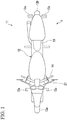
- FIG. 1 is a top view schematically showing a motorcycle that includes the lamp body lighting system 1 in a first embodiment.
- a front wheel 12a and a rear wheel 12b are provided on a vehicle body 12 of a motorcycle 11 as a vehicle.
- a driver who is seated on a seat 13 that is provided on a middle part of the vehicle body 12 operates a handle 14 and allows the motorcycle 11 to travel.
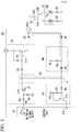
- FIG. 2 is a view showing an example of a schematic configuration of the lamp body lighting system 1 in the first embodiment.
- the lamp body lighting system 1 includes a lamp body 15, a display switch 23, and a lamp body control apparatus 30.
- a right turn signal lamp 15a as the lamp body 15 is provided on a right side at frontward and rearward positions of the vehicle body 12.
- a left turn signal lamp 15b as the lamp body 15 is provided on a left side at frontward and rearward positions of the vehicle body 12.
- a display switch 23 is arranged on a part of the handle 14 of the vehicle body 12 to be operable from the outside of the motorcycle 11.
- the lamp body 15 is a light-emitting diode.
- Two right turn signal lamps 15a are connected in parallel with each other. One of the two right turn signal lamps 15a is arranged at a frontward position of the vehicle body 12. The other of the two right turn signal lamps 15a is arranged at a rearward position of the vehicle body 12. Two left turn signal lamps 15b are connected in parallel with each other. One of the two left turn signal lamps 15b is arranged at a frontward position of the vehicle body 12. The other of the two left turn signal lamps 15b is arranged at a rearward position of the vehicle body 12.
- the display switch 23 is a turn signal switch for allowing any one of the right turn signal lamp 15a and the left turn signal lamp 15b to perform a blinking display, that is, to perform a T/S display.
- the display switch 23 includes a common connection point 23c that is connected to a drive output terminal L, a right connection point 23a that is connected to the right turn signal lamp 15a, and a left connection point 23b that is connected to the left turn signal lamp 15b.
- the common connection point 23c is connected selectively to any one of the right connection point 23a and the left connection point 23b.
- the display switch 23 is switched on, that is, turned on, any one of the right turn signal lamp 15a and the left turn signal lamp 15b is connected to the drive output terminal L.
- the display switch 23 may include a hazard switch for allowing the right turn signal lamp 15a and the left turn signal lamp 15b to perform a blinking display simultaneously, that is, to perform a hazard display. That is, by the driver switching on the display switch 23, the right turn signal lamp 15a and the left turn signal lamp 15b are allowed to perform a blinking display simultaneously, that is, to perform a hazard display, and thereby, the driver may notify an emergency stopping on a road due to a failure and the like of another vehicle and the like.
- a drive electric source terminal B and the drive output terminal L are provided on the lamp body control apparatus 30.
- the drive electric source terminal B is connected to an electric source 5 that is provided on the vehicle body 12.
- an engine (not shown) of the motorcycle 11 is started, and it is possible to supply a voltage VB of the electric source 5 to the lamp body control apparatus 30 via the drive electric source terminal B.
- the electric source 5 is a battery.
- the voltage VB that is supplied to the drive electric source terminal B via the ignition switch 2 from the electric source 5 is output from the drive output terminal L as a blinking signal that blinks the lamp body 15. That is, when the display switch 23 is turned on, the lamp body control apparatus 30 outputs the blinking signal from the drive output terminal L so as to allow at least one of the turn signal lamp 15a and the turn signal lamp 15b to perform a blinking display.
- the lamp body control apparatus 30 includes a control part 31, an output part 32, an input part 33, a self-maintaining part 34, and a level adjustment part 40.
- a status signal that indicates a state of the display switch 23 is output from the input part 33 to the control part 31.
- the control part 31 determines whether or not the display switch 23 is turned on based on the status signal that indicates a state of the display switch 23 and that is output from the input part 33.
- This status signal is a High-Low binarized signal. For example, when the display switch 23 is turned on, the status signal is a High signal. When the display switch 23 is turned off, the status signal is a Low signal. That is, when the status signal that is output from the input part 33 is the High (first logic) signal, the control part 31 determines that the display switch 23 is turned on. On the other hand, when the status signal that is output from the input part 33 is the Low (second logic) signal, the control part 31 determines that the display switch 23 is turned off.
- the control part 31 When it is determined that the display switch 23 is turned on based on the status signal that indicates the state of the display switch 23 and that is output from the input part 33, the control part 31 outputs a blinking command signal that commands a timing of the blinking (hereinafter, referred to as a "blinking timing") of the lamp body 15 to the output part 32.
- the blinking command signal is a High-Low binarized signal.
- the control part 31 When it is determined that the display switch 23 is turned off, the control part 31 outputs a Low signal to the output part 32. That is, when it is determined that the display switch 23 is turned off, the control part 31 does not output the blinking command signal to the output part 32.
- the output part 32 generates a blinking signal that allows the lamp body 15 to blink from the voltage VB on the basis of the blinking command signal that is output from the control part 31. Then, the output part 32 outputs the generated blinking signal from the drive output terminal L.
- the blinking signal is a signal that repeats High (for example, the voltage VB) and Low (for example, 0V) at a constant cycle in response to the blinking timing that is commanded by the blinking command signal. Thereby, the blinking signal is supplied to the lamp body 15 via the display switch 23 that is connected to the drive output terminal L. Thereby, the lamp body 15 blinks at a constant cycle on the basis of the blinking signal that is supplied from the output part 32.
- the output part 32 is a voltage conversion circuit by which a voltage is converted to an output voltage for allowing the lamp body 15 to be lighted or a current amplifier circuit by which a current is amplified to a current for allowing the lamp body 15 to be lighted.
- the input part 33 outputs a status signal that indicates a state of the display switch 23 on the basis of the signal level of the drive output terminal L that is acquired via the level adjustment part 40. That is, the input part 33 outputs a status signal of a first logic which indicates that the state of the display switch 23 is in an ON state when the signal level from the drive output terminal L is a first level. On the other hand, the input part 33 outputs a status signal of a second logic which indicates that the state of the display switch 23 is in an OFF state when the signal level from the drive output terminal L is a second level that is different from the first level.
- the first level corresponds to a signal voltage of substantially 0V, that is, a Low voltage level.
- the second level is a case in which the signal voltage is a voltage VB.
- the voltage VB corresponds to a High voltage level.
- the drive output terminal L is set to be in the first level when the display switch 23 is in an ON state.
- the drive output terminal L is set to be in the second level when the display switch 23 is in an OFF state. Accordingly, when the display switch 23 is in an ON state, a signal of the first level is input to the input part 33 via the level adjustment part 40.
- a signal of the second level is input to the input part 33 via the level adjustment part 40.
- the input part 33 sets two threshold values V th1 , V th2 (V th2 ⁇ V th1 ).
- V th1 is V th2 or more and is a value of the first level or less.
- V th2 is the second level or more and is a value less than V th1 . That is, a signal of V th1 or more is a signal of the first level.
- a signal of V th2 or less is a signal of the second level.
- the status signal is a High-Low binarized signal.
- the input part 33 outputs a High status signal as a status signal which indicates the ON state of the display switch 23 to the control part 31.
- the input part 33 outputs a Low status signal as a status signal which indicates the OFF state of the display switch 23 to the control part 31.
- the level adjustment part 40 outputs a signal of the second level to the input part 33 when detecting a leakage current that occurs on the lamp body 15 side by comparing a preset threshold value to the signal level from the drive output terminal L. For example, the level adjustment part 40 converts the signal level of the signal that is supplied from the drive output terminal L into the second level when detecting a leakage current that occurs on the lamp body 15 side. Then, the level adjustment part 40 outputs the signal that is converted into the second level to the input part 33. Thereby, the level adjustment part 40 prevents erroneous lighting of the lamp body 15 due to the leakage current.
- the control part 31 misidentifies that the display switch 23 is changed to the ON state according to the decrease of the signal level of the drive output terminal L which occurs due to the leakage current. As a result, the control part 31 outputs a blinking command signal and lights the lamp body 15. Accordingly, for example, when the voltage level of the drive output terminal L is decreased due to the leakage current, the level adjustment part 40 converts the signal level of the signal that is supplied from the drive output terminal L into a second level and outputs the signal to the input part 33.
- the level adjustment part 40 when the voltage level of the drive output terminal L is less than a threshold value Vth, the level adjustment part 40 outputs a signal of the first level to the input part 33.
- the threshold value Vth is a value of a voltage that is higher than the voltage of the drive output terminal L that is generated due to the leakage current.
- the self-maintaining part 34 is provided between the output part 32 and the input part 33.
- the logic of the status signal is maintained based on the logic of the blinking command signal.
- the input part 33 outputs a status signal that indicates a state of the display switch 23 on the basis of a signal level of the signal that is output from the level adjustment part 40. For example, when the signal level of the signal that is output from the level adjustment part 40 is equal to or less than V th2 , the input part 33 outputs a status signal which indicates an OFF state of the display switch 23 to the control part 31.
- the signal level of the drive output terminal L becomes equal to or less than V th2 .
- the blinking signal that allows the lamp body 15 to be blinked is a signal that repeats High (for example, the voltage VB) and Low (for example, 0V) at a constant cycle, even when the output part 32 outputs the blinking signal to the lamp body 15 via the drive output terminal L to allow the lamp body 15 to be blinked, there is a case in which the signal level of the drive output terminal L becomes equal to or less than V th2 .
- the input part 33 outputs a status signal which indicates an OFF state of the display switch 23 to the control part 31 and stops the blinking of the lamp body 15.
- the self-maintaining part 34 maintains the logic of the status signal to be High when the lamp body 15 is in a blinking state. Further, when the display switch 23 becomes the OFF state, the self-maintaining part 34 resets a logic maintaining in which the logic of the status signal is maintained to be High.
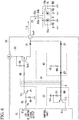
- FIG. 3 is a view showing a circuit example of the lamp body control apparatus 30 in the first embodiment.
- the output part 32 includes resistances R3 to R6, a switching element Tr1, and a switching element Tr2.
- the switching elements Tr1, Tr2 may be constituted of any one of an IGBT (Insulated-Gate Bipolar Transistor), a MOS-FET (Metal-Oxide Semiconductor Field-Effect Transistor), and a BJT (Bipolar Junction Transistor).
- IGBT Insulated-Gate Bipolar Transistor
- MOS-FET Metal-Oxide Semiconductor Field-Effect Transistor
- BJT Bipolar Junction Transistor
- the resistance R3 is an input resistance of the switching element Tr1 and is connected to and between a base of the switching element Tr1 and an output terminal 31a of the control part 31.
- the resistance R4 is connected to and between a base and an emitter of the switching element Tr1.
- the resistance R5 is connected to and between the collector of the switching element Tr1 and a gate of the switching element Tr2.
- the resistance R6 is connected to and between the gate and a source of the switching element Tr2.
- the source of the switching element Tr2 is connected to the drive electric source terminal B, and a drain of the switching element Tr2 is connected to the drive output terminal L via a diode D1.
- the diode D1 is a diode for preventing a back current from the drive output terminal L.
- An anode of the diode D1 is connected to the source of the switching element Tr2, and a cathode of the diode D1 is connected to the drive output terminal L.
- the state between the collector and the emitter of the switching element Tr1 becomes an ON state
- the state between the source and a collector of the switching element Tr2 becomes an ON state
- the voltage VB is applied to the drive output terminal L.
- the state between the collector and the emitter of the switching element Tr1 becomes an OFF state
- the state between the source and the collector of the switching element Tr2 becomes an OFF state, and therefore, in a case where the blinking command signal is output to the control part 31, the voltage 0V is applied to the drive output terminal L.
- the input part 33 includes resistances R7, R8 and a transistor Tr3.
- the transistor Tr3 may be constituted of any one of an IGBT (Insulated-Gate Bipolar Transistor), a MOS-FET (Metal-Oxide Semiconductor Field-Effect Transistor), and a BJT (Bipolar Junction Transistor).
- IGBT Insulated-Gate Bipolar Transistor
- MOS-FET Metal-Oxide Semiconductor Field-Effect Transistor
- BJT Bipolar Junction Transistor
- a first end of the resistance R8 is connected to a base of the switching element Tr3.
- the resistance 7 is connected to and between the base and an emitter of the switching element Tr3.
- the emitter of the switching element Tr3 is connected to an electric source Vcc, and a collector of the switching element Tr3 is connected to the control part 31.
- the electric source Vcc is an electric source voltage that is readable by the control part 31 and is a voltage of a voltage level that is recognized as High by the control part 31. Accordingly, when the display switch 23 is in an OFF state, the base of the switching element Tr3 becomes High, and therefore, the switching element Tr3 becomes an OFF state. Accordingly, a Low status signal is input to an input terminal 31b of the control part 31.
- the self-maintaining part 34 connects the collector of the switching element Tr1 and a point A at a second end of the resistance R8. That is, the self-maintaining part 34 has a function of matching a voltage level (logic) of the collector of the switching element Tr1 with a voltage level (logic) of the second end of the resistance R8. In other words, the self-maintaining part 34 has a function of allowing the voltage level (logic) of the collector of the switching element Tr1 to reflect the voltage level of the second end of the resistance R8.
- the self-maintaining part 34 aims at matching the logic of the voltage level of the collector of the switching element Tr1 with the logic of the voltage level of the point A during the display switch 23 is in an ON state and the High blinking command signal is output from the output terminal 31a of the control part 31.
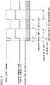
- FIG. 4 is a view showing the self-maintaining part 34 in the first embodiment.
- the control part 31 determines that the display switch 23 is turned on and outputs a blinking command signal from the output terminal 31a.
- this blinking command signal is Low
- the voltage level of the collector of the switching element Tr1 is High. Accordingly, a Low blinking signal is output from the drive output terminal L, and therefore, the voltage level of the drive output terminal L is Low.
- the voltage level of the point A also becomes Low, and a High status signal is input to the input terminal 31b of the control part 31. Accordingly, the control part 31 determines that the display switch 23 is in an ON state and continues outputting the blinking command signal from the output terminal 31a.
- the control part 31 determines that the display switch 23 is in an OFF state and stops outputting the blinking command signal from the output terminal 31a. That is, the control part 31 stops outputting the blinking command signal and stops blinking of the lamp body 15 in spite of the display switch 23 being in the ON state.
- the present embodiment includes the self-maintaining part 34 that matches the voltage level of the collector of the switching element Tr1 with the voltage level of the point A during the High blinking command signal is output from the output terminal 31a of the control part 31. Accordingly, even when the voltage level of the drive output terminal L is High, the voltage level of the point A is maintained to be the voltage level of the collector of the switching element Tr1, that is, Low. Thereby, the High status signal is input to the input terminal 31b of the control part 31. Therefore, even when the blinking command signal is High, it is possible for the control part 31 to determine that the display switch 23 is in an ON state and continue outputting the blinking command signal from the output terminal 31a.
- the level adjustment part 40 includes an electric source part (for example, VB) that is provided in parallel with the lamp body 15, a resistance part (for example, a resistance R9) that is provided in series with the electric source part, and a filter part (for example, D3) that cuts off a voltage decrease of a threshold value or less.
- an electric source part for example, VB
- a resistance part for example, a resistance R9
- a filter part for example, D3 that cuts off a voltage decrease of a threshold value or less.
- the level adjustment part 40 includes the resistance R9 and a Zener diode D3.
- the resistance R9 is a pull-up resistance that pulls up the connection point of an anode of a diode D2 and an anode of the Zener diode D3 to the voltage VB.
- a cathode of the Zener diode D3 is connected to the point A.
- a leakage current from the lamp body control apparatus 30 to the lamp body 15 occurs due to the reduction of an insulation resistance according to degradation of the display switch 23, a case in which the display switch 23 becomes wet with rain, and the like.
- the resistance component of the display switch 23 is a resistance Rs and the leakage current is a leakage current Ir
- the resistance components of the resistances R1, R2 are sufficiently small compared to the resistance Rs and are negligible.
- Vr is represented by the following expression.
- the Zener diode D3 is a diode by which, when a voltage is applied in a reverse direction, a Zener breakdown (avalanche breakdown) occurs at a certain voltage value (hereinafter, referred to as a "Zener voltage"), and it is possible to obtain a constant voltage regardless of a flowing current value.
- the Zener diode D3 is used as a voltage reference. That is, when a voltage potential difference between both ends of the Zener diode D3 exceeds a Zener voltage, the Zener breakdown occurs, that is, the point A is changed to Low.
- the Zener voltage and the resistance value of the resistance R9 are set such that the voltage difference between the voltage of the point A and the voltage Vr of the drive output terminal L that occurs by the leakage current Ir becomes the Zener voltage or less.
- the level adjustment part 40 includes a function of changing the voltage level of the point A to Low when the voltage of the drive output terminal L becomes less than the threshold value Vth that is set in advance.
- the lamp body control apparatus 30 in the first embodiment is a lamp body control apparatus that controls, in accordance with an operation of a display switch that is provided on a vehicle, blinking of a lamp body that is provided on the vehicle, the lamp body control apparatus 30 including: an output part 32 that outputs a blinking signal which blinks the lamp body 15 to the lamp body 15 from a drive output terminal L based on a blinking command signal that commands a blinking timing of the lamp body 15; an input part 33 that outputs a status signal of a first logic which indicates that a state of the display switch 23 is in an ON state when a signal level from the drive output terminal L is a first level and that outputs a status signal of a second logic which indicates that a state of the display switch 23 is in an OFF state when the signal level from the drive output terminal L is a second level that is different from the first level; a control part 31 that outputs the blinking command signal to the output part 32 when a logic of the status signal that is output from the input part 33 is the
- the level adjustment part 40 outputs a signal of the second level to the input part 33 when detecting a leakage current that occurs on the lamp body 15 side by comparing the threshold value Vth to the signal level from the drive output terminal. Thereby, it is possible to prevent erroneous lighting of the lamp body 15 due to the leakage current.
- the resistance R9 of the level adjustment part 40 or the Zener voltage of the Zener diode D3 it is possible to easily adjust a detection sensitivity for detecting that the insulation property of the display switch 23 is decreased due to rainwater and the like. Accordingly, it is possible to easily adjust the threshold value Vth, the degree of freedom of the lamp body 15 is increased, and it is possible to contribute to the reduction of the size and the weight of the lamp body 15.
- the lamp body control apparatus 30 in the first embodiment to prevent a blinking operation of the lamp body at an unintended timing of a user without separately providing a sensor that detects a leakage current which occurs on the lamp body 15 side.
- the lamp body control apparatus 30 in the first embodiment includes the level adjustment part 40 that detects a leakage current inside the lamp body control apparatus 30, and therefore, it becomes possible to downsize the lamp body 15 compared to a case of the related art in which the lamp body 15 includes a function of detecting a leakage current.
- the self-maintaining part 34 it becomes possible for the lamp body control apparatus 30 in the first embodiment to maintain the signal level of the status signal after blinking of the lamp body 15 is started, and it is possible to integrate the output part 32 and the input part 33, that is, to share the output of the output part 32 and the input of the input part 33.
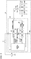
- FIG. 5 is a view showing an example of a schematic configuration of a lamp body lighting system 1A in a second embodiment.
- the lamp body lighting system 1A in the second embodiment has a configuration in which the detection performance of a leakage current in the level adjustment part 40 is further improved compared to the first embodiment.
- the lamp body lighting system 1A includes the lamp body 15, the display switch 23, the lamp body control apparatus, and a bias resistance RB.
- FIG. 5 is a view showing a circuit example of the lamp body lighting system 1A in the second embodiment.
- the lamp body lighting system 1 in the first embodiment even when seawater, rainwater, and the like enter the inside of the display switch 23 and the resistance value of the insulation resistance becomes relatively low, it is desirable that the lamp body 15 be not erroneously lighted. That is, even when seawater, rainwater, and the like enter the inside of the display switch 23 and the resistance value of the insulation resistance becomes relatively low, it is desirable that it be recognized that a leakage current due to insulation degradation of the display switch 23 has occurred, and a Low status signal be input to the input terminal 31b of the control part 31. In that case, by increasing a current Iin that flows out toward the lamp body 15 side from the drive output terminal L, the threshold value Vth is decreased.
- the lamp body lighting system 1A in the second embodiment includes the bias resistance RB that is connected in parallel with respect to the lamp body 15 so as to prevent the dimming of the lamp body 15 by the current Iin.
- the lamp body lighting system 1A in the second embodiment includes a bias resistance that is connected in parallel with respect to the lamp body 15. Accordingly, the lamp body lighting system 1A provides an advantage similar to the first embodiment, and it is possible to improve the accuracy of the leakage current in the level adjustment part 40 while preventing the dimming of the lamp body 15 by the current Iin.
- Each part of the lamp body control apparatus 30 may be realized by hardware, may be realized by software, or may be realized by the combination of hardware and software.
- the lamp body control apparatus 30 in the embodiments described above may be realized by a computer.
- a program for realizing this function may be recorded in a computer-readable recording medium, and the program recorded in the recording medium may be read into and executed on a computer system to thereby realize the function.
- the term "computer system” used herein includes an OS or hardware such as peripherals.
- the term "computer-readable recording medium” refers to portable media such as a flexible disk, a magneto-optical disc, a ROM, and a CD-ROM and a storage device such as a hard disk embedded in the computer system.
- the term "computer-readable recording medium” may include a recording medium that holds a program dynamically for a short period of time like a network such as the Internet or a communication line when a program is transmitted through a communication line such as a telephone line and may include a recording medium that stores a program for a certain period of time like a volatile memory in a computer system which serves as a server or a client in that case.
- the above program may be a program for realizing some of the functions described above, may be a program capable of realizing the above functions by the combination with a program already recorded in the computer system, or may be a program that is realized by using a programmable logic device such as a FPGA (Field-Programmable Gate Array).
Landscapes
- Engineering & Computer Science (AREA)
- Mechanical Engineering (AREA)
- Lighting Device Outwards From Vehicle And Optical Signal (AREA)
Abstract
Description
- The present invention relates to a lamp body control apparatus and a lamp body lighting system.
- Priority is claimed on Japanese Patent Application No.
2016-110159 filed on June 1, 2016 2016-110160 filed on June 1, 2016 - In the related art, a lamp body lighting system is known in which, when a turn signal switch that is provided on a vehicle is operated, a winker lamp (lamp body) that corresponds to the operated turn signal switch starts blinking, and thereby, a proceeding direction of a vehicle is indicated externally (for example, refer to Patent Document 1).
- Further, in a lamp body lighting system, there may be a case in which, for example, a turn signal switch conducts due to rainwater, splash, and the like, a leakage current flows to a lamp body side, and the lamp body is erroneously lighted at an unintended timing by a user. Therefore, the lamp body lighting system described in
Patent Document 1 includes a leakage current prevention means that detects a leakage current and that prevents erroneous lighting of the lamp body due to the leakage current. -
FIG. 7 is a view showing an example of a schematic configuration of a lamp body lighting system of the related art. The lampbody lighting system 100 includes alamp body 102, aturn signal switch 103, and a lampbody control apparatus 104. - The
turn signal switch 103 is provided between thelamp body 102 and abattery 101 that is provided on a vehicle. Theturn signal switch 103 is operated by a user and thereby allows any one of right andleft light bodies 102 to be displayed to be blinked. Further, the lampbody control apparatus 104 includes acontrol IC 201 and a turn signal relay (relay part) 202 that is provided between thebattery 101 and theturn signal switch 103. - In the lamp
body control apparatus 104, when theturn signal switch 103 is operated to any of the right direction and the left direction, thelamp body 102 that corresponds to the operated direction is connected to thebattery 101 via theturn signal switch 103, a relay is operated to be opened or closed on the basis of a blinking signal that is output from thecontrol IC 201, and thelamp body 102 of the desired direction is displayed to be blinked (T/S display). - [Patent Document 1] Japanese Unexamined Patent Application, First Publication No.
2013-33610 - However, in the lamp
body control apparatus 104 of the related art, when anignition switch 300 is turned on (when an engine is started), a blinking signal that allows the lamp body to be displayed to be blinked is output from thecontrol IC 201 to therelay part 202. Therefore, depending on a timing when theturn signal switch 103 is operated by a user, a difference in a timing when thelamp body 102 is blinked occurs.FIG. 8 is a view showing a timing when thelamp body 102 is lighted in the lampbody control apparatus 104 of the related art. - As shown in
FIG. 8 , when a user turns on theignition switch 300 at a time point t10 and the engine is started, thecontrol IC 201 outputs a rectangular-wave blinking signal to therelay part 202. When the user turns on theturn signal switch 103 at a time point t11, therelay part 202 outputs a drive voltage that is synchronized with the blinking signal to thelamp body 102. Accordingly, thelamp body 102 is lighted later by a time ΔT10 from the time point t11. However, when the user turns on theturn signal switch 103 at a time point t12, thelamp body 102 is lighted later by a time ΔT20 which is shorter than the time ΔT10 from the time point t12. That is, dispersion of a time from when theturn signal switch 103 is turned on to when thelamp body 102 is lighted occurs. Further, when the user turns on theturn signal switch 103 at a time point t13, thelamp body 102 is lighted at the time point t13 when theturn signal switch 103 is turned on, and soon thelamp body 102 is turned off. That is, there is a possibility that, depending on a timing when theturn signal switch 103 is operated by a user, a difference in a timing when thelamp body 102 is turned off occurs. - Accordingly, in order to solve the problem described above, it is necessary to provide an input part that notifies the lamp
body control apparatus 104 of theturn signal switch 103 being turned on. Therefore, it is necessary to increase a terminal that is connected to the input part in the lampbody control apparatus 104, and there is a problem in that the size of the lampbody control apparatus 104 is increased. - An object of an aspect of the present invention is to provide a lamp body control apparatus and a lamp body lighting system in which a blinking timing of a lamp body is constant independently of a timing when a turn signal switch is operated by a user while preventing a size increase.
- Further, a novel lamp body control apparatus is required in which a blinking timing of a lamp body is constant independently of a timing when a turn signal switch is operated by a user without increasing the number of terminals.
- However, when a leakage current prevention means of the related art is applied to the novel lamp body control apparatus described above, it is necessary to add a new terminal of the lamp body control apparatus, and there is a problem in that the size of the lamp body control apparatus is increased.
- Another object of an aspect of the present invention is to provide a lamp body control apparatus and a lamp body lighting system capable of preventing erroneous lighting of a lamp body due to a leakage current while preventing a size increase.
- An aspect of the present invention is a lamp body control apparatus that controls, in accordance with an operation of a display switch that is provided on a vehicle, blinking of a lamp body that is provided on the vehicle, the lamp body control apparatus including: an output part that outputs a blinking signal which blinks the lamp body to the lamp body from a drive output terminal based on a blinking command signal that commands a blinking timing of the lamp body; an input part that outputs a status signal of a first logic which indicates that a state of the display switch is in an ON state when a signal level from the drive output terminal is a first level and that outputs a status signal of a second logic which indicates that a state of the display switch is in an OFF state when the signal level is a second level that is different from the first level; a control part that outputs the blinking command signal to the output part when a logic of the status signal that is output from the input part is the first logic; and a self-maintaining part that maintains a logic of the status signal based on a logic of the blinking command signal when the lamp body is in a blinking state.
- In the lamp body control apparatus described above, the self-maintaining part may be provided between the output part and the input part.
- In the lamp body control apparatus described above, the output part and the input part may be connected to the drive output terminal such that a logic that allows the lamp body to be lighted in the blinking signal and a logic which indicates that the display switch is in an ON state in the status signal are matched with each other.
- The lamp body control apparatus described above may further include a level adjustment part that outputs a signal of the second level to the input part when detecting a leakage current that occurs on the lamp body side by comparing a preset threshold value to the signal level from the drive output terminal.
- In the lamp body control apparatus described above, the level adjustment part may be provided between the input part and the drive output terminal, may output a signal of the second level to the input part when the signal level from the drive output terminal is less than the threshold value, and may output a signal of the first level to the input part when the signal level is equal to or more than the threshold value.
- In the lamp body control apparatus described above, the self-maintaining part may be provided between the output part and a connection point of the input part and the level adjustment part.
- In the lamp body control apparatus described above, the output part and the input part may be connected to the drive output terminal such that a logic that allows the lamp body to be lighted in the blinking signal and a logic which indicates that the display switch is in an ON state in the status signal are matched with each other.
- Another aspect of the present invention is a lamp body lighting system that includes: a lamp body control apparatus described above; and a lamp body that blinks based on a blinking signal which is output via the drive output terminal from the lamp body control apparatus.
- The lamp body lighting system described above may further include a bias resistance that is connected in parallel with respect to the lamp body.
- According to an aspect of the present invention, it is possible to provide a lamp body control apparatus and a lamp body lighting system in which a blinking timing of a lamp body is constant independently of a timing when a turn signal switch is operated by a user while preventing a size increase.
- Further, according to an aspect of the present invention, it is possible to provide a lamp body control apparatus and a lamp body lighting system capable of preventing erroneous lighting of a lamp body due to a leakage current while preventing a size increase.
-
-
FIG. 1 is a top view schematically showing a motorcycle that includes a lamp body lighting system in a first embodiment. -
FIG. 2 is a view showing an example of a schematic configuration of the lamp body lighting system in the first embodiment. -
FIG. 3 is a view showing a circuit example of a lamp body control apparatus in the first embodiment. -
FIG. 4 is a view showing a self-maintaining part in the first embodiment. -
FIG. 5 is a view showing an example of a schematic configuration of a lamp body lighting system in a second embodiment. -
FIG. 6 is a view showing a circuit example of the lamp body lighting system in the second embodiment. -
FIG. 7 is a view showing an example of a schematic configuration of a lamp body lighting system of the related art. -
FIG. 8 is a view showing a timing when a lamp body is lighted in a lamp body control apparatus of the related art. - Hereinafter, embodiments of the present invention are described, but the following embodiments do not limit the invention according to claims. Further, all of the combinations of features described in the embodiments are not necessarily indispensable for solving the problem addressed by the invention. In the drawings, the same reference numerals may be given to the same or similar parts, and redundant descriptions may be omitted.
- Hereinafter, a lamp
body lighting system 1 of an embodiment is described with reference to the drawings. -
FIG. 1 is a top view schematically showing a motorcycle that includes the lampbody lighting system 1 in a first embodiment. As shown inFIG. 1 , afront wheel 12a and arear wheel 12b are provided on avehicle body 12 of a motorcycle 11 as a vehicle. A driver who is seated on aseat 13 that is provided on a middle part of thevehicle body 12 operates ahandle 14 and allows the motorcycle 11 to travel. -
FIG. 2 is a view showing an example of a schematic configuration of the lampbody lighting system 1 in the first embodiment. - As shown in
FIG. 1 andFIG. 2 , the lampbody lighting system 1 includes alamp body 15, adisplay switch 23, and a lampbody control apparatus 30. - As shown in
FIG. 1 , a rightturn signal lamp 15a as thelamp body 15 is provided on a right side at frontward and rearward positions of thevehicle body 12. A leftturn signal lamp 15b as thelamp body 15 is provided on a left side at frontward and rearward positions of thevehicle body 12. As shown inFIG. 1 , adisplay switch 23 is arranged on a part of thehandle 14 of thevehicle body 12 to be operable from the outside of the motorcycle 11. For example, thelamp body 15 is a light-emitting diode. - Two right
turn signal lamps 15a are connected in parallel with each other. One of the two rightturn signal lamps 15a is arranged at a frontward position of thevehicle body 12. The other of the two rightturn signal lamps 15a is arranged at a rearward position of thevehicle body 12. Two leftturn signal lamps 15b are connected in parallel with each other. One of the two leftturn signal lamps 15b is arranged at a frontward position of thevehicle body 12. The other of the two leftturn signal lamps 15b is arranged at a rearward position of thevehicle body 12. - By a driver operating the
display switch 23, it is possible to allow any one of the rightturn signal lamp 15a and the leftturn signal lamp 15b to perform a blinking display, that is, to perform a turn signal display (T/S display), and it is possible to notify another vehicle and the like of a proceeding direction of the motorcycle 11. That is, thedisplay switch 23 is a turn signal switch for allowing any one of the rightturn signal lamp 15a and the leftturn signal lamp 15b to perform a blinking display, that is, to perform a T/S display. - As shown in
FIG. 2 , for example, thedisplay switch 23 includes acommon connection point 23c that is connected to a drive output terminal L, aright connection point 23a that is connected to the rightturn signal lamp 15a, and aleft connection point 23b that is connected to the leftturn signal lamp 15b. When thedisplay switch 23 is switched on (operated) by an operation of the driver, thecommon connection point 23c is connected selectively to any one of theright connection point 23a and theleft connection point 23b. When thedisplay switch 23 is switched on, that is, turned on, any one of the rightturn signal lamp 15a and the leftturn signal lamp 15b is connected to the drive output terminal L. Then, the rightturn signal lamp 15a or the leftturn signal lamp 15b that is connected to the drive output terminal L is blinked on the basis of a blinking signal that is output from the lampbody control apparatus 30. Thedisplay switch 23 may include a hazard switch for allowing the rightturn signal lamp 15a and the leftturn signal lamp 15b to perform a blinking display simultaneously, that is, to perform a hazard display. That is, by the driver switching on thedisplay switch 23, the rightturn signal lamp 15a and the leftturn signal lamp 15b are allowed to perform a blinking display simultaneously, that is, to perform a hazard display, and thereby, the driver may notify an emergency stopping on a road due to a failure and the like of another vehicle and the like. - As shown in
FIG. 2 , a drive electric source terminal B and the drive output terminal L are provided on the lampbody control apparatus 30. The drive electric source terminal B is connected to anelectric source 5 that is provided on thevehicle body 12. In the present embodiment, by the driver switching on anignition switch 2, an engine (not shown) of the motorcycle 11 is started, and it is possible to supply a voltage VB of theelectric source 5 to the lampbody control apparatus 30 via the drive electric source terminal B. For example, theelectric source 5 is a battery. The voltage VB that is supplied to the drive electric source terminal B via theignition switch 2 from theelectric source 5 is output from the drive output terminal L as a blinking signal that blinks thelamp body 15. That is, when thedisplay switch 23 is turned on, the lampbody control apparatus 30 outputs the blinking signal from the drive output terminal L so as to allow at least one of theturn signal lamp 15a and theturn signal lamp 15b to perform a blinking display. - As shown in
FIG. 2 , the lampbody control apparatus 30 includes acontrol part 31, anoutput part 32, aninput part 33, a self-maintainingpart 34, and alevel adjustment part 40. - A status signal that indicates a state of the
display switch 23 is output from theinput part 33 to thecontrol part 31. - The
control part 31 determines whether or not thedisplay switch 23 is turned on based on the status signal that indicates a state of thedisplay switch 23 and that is output from theinput part 33. This status signal is a High-Low binarized signal. For example, when thedisplay switch 23 is turned on, the status signal is a High signal. When thedisplay switch 23 is turned off, the status signal is a Low signal. That is, when the status signal that is output from theinput part 33 is the High (first logic) signal, thecontrol part 31 determines that thedisplay switch 23 is turned on. On the other hand, when the status signal that is output from theinput part 33 is the Low (second logic) signal, thecontrol part 31 determines that thedisplay switch 23 is turned off. - When it is determined that the
display switch 23 is turned on based on the status signal that indicates the state of thedisplay switch 23 and that is output from theinput part 33, thecontrol part 31 outputs a blinking command signal that commands a timing of the blinking (hereinafter, referred to as a "blinking timing") of thelamp body 15 to theoutput part 32. For example, the blinking command signal is a High-Low binarized signal. When it is determined that thedisplay switch 23 is turned off, thecontrol part 31 outputs a Low signal to theoutput part 32. That is, when it is determined that thedisplay switch 23 is turned off, thecontrol part 31 does not output the blinking command signal to theoutput part 32. - The
output part 32 generates a blinking signal that allows thelamp body 15 to blink from the voltage VB on the basis of the blinking command signal that is output from thecontrol part 31. Then, theoutput part 32 outputs the generated blinking signal from the drive output terminal L. For example, the blinking signal is a signal that repeats High (for example, the voltage VB) and Low (for example, 0V) at a constant cycle in response to the blinking timing that is commanded by the blinking command signal. Thereby, the blinking signal is supplied to thelamp body 15 via thedisplay switch 23 that is connected to the drive output terminal L. Thereby, thelamp body 15 blinks at a constant cycle on the basis of the blinking signal that is supplied from theoutput part 32. For example, theoutput part 32 is a voltage conversion circuit by which a voltage is converted to an output voltage for allowing thelamp body 15 to be lighted or a current amplifier circuit by which a current is amplified to a current for allowing thelamp body 15 to be lighted. - The
input part 33 outputs a status signal that indicates a state of thedisplay switch 23 on the basis of the signal level of the drive output terminal L that is acquired via thelevel adjustment part 40. That is, theinput part 33 outputs a status signal of a first logic which indicates that the state of thedisplay switch 23 is in an ON state when the signal level from the drive output terminal L is a first level. On the other hand, theinput part 33 outputs a status signal of a second logic which indicates that the state of thedisplay switch 23 is in an OFF state when the signal level from the drive output terminal L is a second level that is different from the first level. For example, the first level corresponds to a signal voltage of substantially 0V, that is, a Low voltage level. The second level is a case in which the signal voltage is a voltage VB. For example, the voltage VB corresponds to a High voltage level. - For example, the drive output terminal L is set to be in the first level when the
display switch 23 is in an ON state. On the other hand, the drive output terminal L is set to be in the second level when thedisplay switch 23 is in an OFF state. Accordingly, when thedisplay switch 23 is in an ON state, a signal of the first level is input to theinput part 33 via thelevel adjustment part 40. On the other hand, when thedisplay switch 23 is in an OFF state, a signal of the second level is input to theinput part 33 via thelevel adjustment part 40. - For example, the
input part 33 sets two threshold values Vth1, Vth2 (Vth2<Vth1). When the voltage level of the drive output terminal L is equal to or more than Vth1, theinput part 33 outputs the status signal which indicates the ON state of thedisplay switch 23 to thecontrol part 31. On the other hand, when the voltage level of the drive output terminal L is equal to or less than Vth2, theinput part 33 outputs the status signal which indicates the OFF state of thedisplay switch 23 to thecontrol part 31. In this case, Vth1 is Vth2 or more and is a value of the first level or less. Vth2 is the second level or more and is a value less than Vth1. That is, a signal of Vth1 or more is a signal of the first level. A signal of Vth2 or less is a signal of the second level. - For example, the status signal is a High-Low binarized signal. For example, the
input part 33 outputs a High status signal as a status signal which indicates the ON state of thedisplay switch 23 to thecontrol part 31. On the other hand, theinput part 33 outputs a Low status signal as a status signal which indicates the OFF state of thedisplay switch 23 to thecontrol part 31. - The
level adjustment part 40 outputs a signal of the second level to theinput part 33 when detecting a leakage current that occurs on thelamp body 15 side by comparing a preset threshold value to the signal level from the drive output terminal L. For example, thelevel adjustment part 40 converts the signal level of the signal that is supplied from the drive output terminal L into the second level when detecting a leakage current that occurs on thelamp body 15 side. Then, thelevel adjustment part 40 outputs the signal that is converted into the second level to theinput part 33. Thereby, thelevel adjustment part 40 prevents erroneous lighting of thelamp body 15 due to the leakage current. - For example, in general, there is a case in which a leakage current flows to the
lamp body 15 side due to an external factor such as the weather. As shown inFIG. 1 , in the motorcycle 11, since thedisplay switch 23 is provided in the vicinity of thehandle 14, when thedisplay switch 23 becomes wet with rain and a leakage current occurs, there is a possibility that thelamp body 15 is erroneously lighted due to the leakage current. For example, when the leakage current flows to thelamp body 15 side, the signal level of the drive output terminal L is decreased. Accordingly, when it is determined whether thedisplay switch 23 is in an ON state or in an OFF state based on the signal level of the drive output terminal L, thecontrol part 31 misidentifies that thedisplay switch 23 is changed to the ON state according to the decrease of the signal level of the drive output terminal L which occurs due to the leakage current. As a result, thecontrol part 31 outputs a blinking command signal and lights thelamp body 15. Accordingly, for example, when the voltage level of the drive output terminal L is decreased due to the leakage current, thelevel adjustment part 40 converts the signal level of the signal that is supplied from the drive output terminal L into a second level and outputs the signal to theinput part 33. For example, when the voltage level of the drive output terminal L is less than a threshold value Vth, thelevel adjustment part 40 outputs a signal of the first level to theinput part 33. On the other hand, when the voltage level of the drive output terminal L is the threshold value Vth or more, thelevel adjustment part 40 outputs a signal of the second level to theinput part 33. The threshold value Vth is a value of a voltage that is higher than the voltage of the drive output terminal L that is generated due to the leakage current. - The self-maintaining
part 34 is provided between theoutput part 32 and theinput part 33. When thelamp body 15 is in a blinking state, the logic of the status signal is maintained based on the logic of the blinking command signal. As described above, theinput part 33 outputs a status signal that indicates a state of thedisplay switch 23 on the basis of a signal level of the signal that is output from thelevel adjustment part 40. For example, when the signal level of the signal that is output from thelevel adjustment part 40 is equal to or less than Vth2, theinput part 33 outputs a status signal which indicates an OFF state of thedisplay switch 23 to thecontrol part 31. However, there is a case in which, when thedisplay switch 23 is in an ON state, the signal level of the drive output terminal L becomes equal to or less than Vth2. - That is, since the blinking signal that allows the
lamp body 15 to be blinked is a signal that repeats High (for example, the voltage VB) and Low (for example, 0V) at a constant cycle, even when theoutput part 32 outputs the blinking signal to thelamp body 15 via the drive output terminal L to allow thelamp body 15 to be blinked, there is a case in which the signal level of the drive output terminal L becomes equal to or less than Vth2. In this case, theinput part 33 outputs a status signal which indicates an OFF state of thedisplay switch 23 to thecontrol part 31 and stops the blinking of thelamp body 15. That is, there is a possibility that theinput part 33 recognizes that thedisplay switch 23 is in the OFF state in spite of thedisplay switch 23 being in the ON state. In order to solve this problem, the self-maintainingpart 34 maintains the logic of the status signal to be High when thelamp body 15 is in a blinking state. Further, when thedisplay switch 23 becomes the OFF state, the self-maintainingpart 34 resets a logic maintaining in which the logic of the status signal is maintained to be High. - Hereinafter, a circuit example of the lamp
body control apparatus 30 in the present embodiment is described.FIG. 3 is a view showing a circuit example of the lampbody control apparatus 30 in the first embodiment. - The
output part 32 includes resistances R3 to R6, a switching element Tr1, and a switching element Tr2. The switching elements Tr1, Tr2 may be constituted of any one of an IGBT (Insulated-Gate Bipolar Transistor), a MOS-FET (Metal-Oxide Semiconductor Field-Effect Transistor), and a BJT (Bipolar Junction Transistor). The present embodiment is described using a case in which the switching element Tr1 is a NPN-type BJT, and the switching element Tr2 is a P-channel MOS-FET. - The resistance R3 is an input resistance of the switching element Tr1 and is connected to and between a base of the switching element Tr1 and an
output terminal 31a of thecontrol part 31. The resistance R4 is connected to and between a base and an emitter of the switching element Tr1. Thereby, when a High blinking command signal is output to the switching element TR1 via the resistance R3 from theoutput terminal 31a of thecontrol part 31, the state between a collector and the emitter of the switching element Tr1 becomes an ON state. On the other hand, when a Low blinking command signal is output to the switching element Tr1 via the resistance R3 from theoutput terminal 31a of thecontrol part 31, the state between the collector and the emitter of the switching element Tr1 becomes an OFF state. - The resistance R5 is connected to and between the collector of the switching element Tr1 and a gate of the switching element Tr2. The resistance R6 is connected to and between the gate and a source of the switching element Tr2. The source of the switching element Tr2 is connected to the drive electric source terminal B, and a drain of the switching element Tr2 is connected to the drive output terminal L via a diode D1. The diode D1 is a diode for preventing a back current from the drive output terminal L. An anode of the diode D1 is connected to the source of the switching element Tr2, and a cathode of the diode D1 is connected to the drive output terminal L. Thereby, when the state between the collector and the emitter of the switching element Tr1 becomes an ON state, the state between the source and a collector of the switching element Tr2 becomes an ON state, and therefore, the voltage VB is applied to the drive output terminal L. On the other hand, when the state between the collector and the emitter of the switching element Tr1 becomes an OFF state, the state between the source and the collector of the switching element Tr2 becomes an OFF state, and therefore, in a case where the blinking command signal is output to the
control part 31, the voltage 0V is applied to the drive output terminal L. - The
input part 33 includes resistances R7, R8 and a transistor Tr3. The transistor Tr3 may be constituted of any one of an IGBT (Insulated-Gate Bipolar Transistor), a MOS-FET (Metal-Oxide Semiconductor Field-Effect Transistor), and a BJT (Bipolar Junction Transistor). The present embodiment is described using a case in which the switching element Tr3 is a PNP-type BJT. - A first end of the resistance R8 is connected to a base of the switching element Tr3. The resistance 7 is connected to and between the base and an emitter of the switching element Tr3. The emitter of the switching element Tr3 is connected to an electric source Vcc, and a collector of the switching element Tr3 is connected to the
control part 31. The electric source Vcc is an electric source voltage that is readable by thecontrol part 31 and is a voltage of a voltage level that is recognized as High by thecontrol part 31. Accordingly, when thedisplay switch 23 is in an OFF state, the base of the switching element Tr3 becomes High, and therefore, the switching element Tr3 becomes an OFF state. Accordingly, a Low status signal is input to aninput terminal 31b of thecontrol part 31. On the other hand, when thedisplay switch 23 is operated from an OFF state to an ON state, the base of the switching element Tr3 is changed from High to Low, and therefore, the switching element Tr3 is changed from an OFF state to an ON state. Accordingly, a High status signal is input to theinput terminal 31b of thecontrol part 31. - The self-maintaining
part 34 connects the collector of the switching element Tr1 and a point A at a second end of the resistance R8. That is, the self-maintainingpart 34 has a function of matching a voltage level (logic) of the collector of the switching element Tr1 with a voltage level (logic) of the second end of the resistance R8. In other words, the self-maintainingpart 34 has a function of allowing the voltage level (logic) of the collector of the switching element Tr1 to reflect the voltage level of the second end of the resistance R8. The self-maintainingpart 34 aims at matching the logic of the voltage level of the collector of the switching element Tr1 with the logic of the voltage level of the point A during thedisplay switch 23 is in an ON state and the High blinking command signal is output from theoutput terminal 31a of thecontrol part 31. -
FIG. 4 is a view showing the self-maintainingpart 34 in the first embodiment. - As shown in
FIG. 4 , when thedisplay switch 23 is operated to ON, the voltage level of the drive output terminal L is changed from High to Low. Then, the voltage level of the point A is changed from High to Low, and the High status signal is input to theinput terminal 31b of thecontrol part 31. Therefore, thecontrol part 31 determines that thedisplay switch 23 is turned on and outputs a blinking command signal from theoutput terminal 31a. When this blinking command signal is Low, the voltage level of the collector of the switching element Tr1 is High. Accordingly, a Low blinking signal is output from the drive output terminal L, and therefore, the voltage level of the drive output terminal L is Low. Accordingly, the voltage level of the point A also becomes Low, and a High status signal is input to theinput terminal 31b of thecontrol part 31. Accordingly, thecontrol part 31 determines that thedisplay switch 23 is in an ON state and continues outputting the blinking command signal from theoutput terminal 31a. - On the other hand, when the blinking command signal is High, the voltage level of the collector of the switching element Tr1 is Low. Accordingly, a High blinking signal is output from the drive output terminal L, and therefore, the voltage level of the drive output terminal L is High. When the self-maintaining
part 34 is not present, the voltage level of the point A also becomes High, and a Low status signal is input to theinput terminal 31b of thecontrol part 31. Accordingly, thecontrol part 31 determines that thedisplay switch 23 is in an OFF state and stops outputting the blinking command signal from theoutput terminal 31a. That is, thecontrol part 31 stops outputting the blinking command signal and stops blinking of thelamp body 15 in spite of thedisplay switch 23 being in the ON state. The present embodiment includes the self-maintainingpart 34 that matches the voltage level of the collector of the switching element Tr1 with the voltage level of the point A during the High blinking command signal is output from theoutput terminal 31a of thecontrol part 31. Accordingly, even when the voltage level of the drive output terminal L is High, the voltage level of the point A is maintained to be the voltage level of the collector of the switching element Tr1, that is, Low. Thereby, the High status signal is input to theinput terminal 31b of thecontrol part 31. Therefore, even when the blinking command signal is High, it is possible for thecontrol part 31 to determine that thedisplay switch 23 is in an ON state and continue outputting the blinking command signal from theoutput terminal 31a. - For example, the
level adjustment part 40 includes an electric source part (for example, VB) that is provided in parallel with thelamp body 15, a resistance part (for example, a resistance R9) that is provided in series with the electric source part, and a filter part (for example, D3) that cuts off a voltage decrease of a threshold value or less. - Specifically, the
level adjustment part 40 includes the resistance R9 and a Zener diode D3. - The resistance R9 is a pull-up resistance that pulls up the connection point of an anode of a diode D2 and an anode of the Zener diode D3 to the voltage VB.
- A cathode of the Zener diode D3 is connected to the point A.
- Hereinafter, a detection method of a leakage current in the
level adjustment part 40 is described. - For example, a leakage current from the lamp
body control apparatus 30 to thelamp body 15 occurs due to the reduction of an insulation resistance according to degradation of thedisplay switch 23, a case in which thedisplay switch 23 becomes wet with rain, and the like. At this time, when the resistance component of thedisplay switch 23 is a resistance Rs and the leakage current is a leakage current Ir, a voltage of Vr = Rs × Ir occurs at the drive output terminal L. In the present embodiment, the resistance components of the resistances R1, R2 are sufficiently small compared to the resistance Rs and are negligible. Here, Vr is represented by the following expression.
- Accordingly, it becomes possible by the resistance value of the resistance Rs to adjust the voltage Vr of the drive output terminal L that occurs by the leakage current Ir.
- The Zener diode D3 is a diode by which, when a voltage is applied in a reverse direction, a Zener breakdown (avalanche breakdown) occurs at a certain voltage value (hereinafter, referred to as a "Zener voltage"), and it is possible to obtain a constant voltage regardless of a flowing current value. The Zener diode D3 is used as a voltage reference. That is, when a voltage potential difference between both ends of the Zener diode D3 exceeds a Zener voltage, the Zener breakdown occurs, that is, the point A is changed to Low. Accordingly, the Zener voltage and the resistance value of the resistance R9 are set such that the voltage difference between the voltage of the point A and the voltage Vr of the drive output terminal L that occurs by the leakage current Ir becomes the Zener voltage or less. Thereby, in a state where the
display switch 23 is in an OFF state, even when the voltage Vr occurs at the drive output terminal L by the leakage current Ir, since the point A is not changed to Low, the signal level that is input to theinput part 33 is equal to or more than Vth1, and erroneous lighting of thelamp body 15 is prevented. When the drive output terminal L becomes Low, which is a voltage that is sufficiently lower than Vr by thedisplay switch 23 being turned on, since the Zener breakdown (avalanche breakdown) occurs and the point A is changed to Low, the signal level that is input to theinput part 33 becomes equal to or less than Vth2. Thereby, when thedisplay switch 23 is turned on, it is possible for the lampbody control apparatus 30 to reliably blink thelamp body 15. In other words, thelevel adjustment part 40 includes a function of changing the voltage level of the point A to Low when the voltage of the drive output terminal L becomes less than the threshold value Vth that is set in advance. - As described above, the lamp body control apparatus 30 in the first embodiment is a lamp body control apparatus that controls, in accordance with an operation of a display switch that is provided on a vehicle, blinking of a lamp body that is provided on the vehicle, the lamp body control apparatus 30 including: an output part 32 that outputs a blinking signal which blinks the lamp body 15 to the lamp body 15 from a drive output terminal L based on a blinking command signal that commands a blinking timing of the lamp body 15; an input part 33 that outputs a status signal of a first logic which indicates that a state of the display switch 23 is in an ON state when a signal level from the drive output terminal L is a first level and that outputs a status signal of a second logic which indicates that a state of the display switch 23 is in an OFF state when the signal level from the drive output terminal L is a second level that is different from the first level; a control part 31 that outputs the blinking command signal to the output part 32 when a logic of the status signal that is output from the input part 33 is the first logic; and a level adjustment part 40 that converts the signal level from the drive output terminal L into the second level and outputs the signal that is converted to the second level to the input part 33 when detecting a leakage current that occurs on the lamp body 15 side by comparing a preset threshold value Vth to the signal level from the drive output terminal L.
- Thereby, it is possible to detect that the
display switch 23 is turned on based on the signal level that is supplied from the drive output terminal L, and therefore, it is possible to allow the blinking timing of thelamp body 15 to be constant without adding a new terminal. Therefore, it is possible to control the blinking timing of the lamp body to be constant independently of a timing when the turn signal switch is operated by a user while preventing a size increase. Further, thelevel adjustment part 40 outputs a signal of the second level to theinput part 33 when detecting a leakage current that occurs on thelamp body 15 side by comparing the threshold value Vth to the signal level from the drive output terminal. Thereby, it is possible to prevent erroneous lighting of thelamp body 15 due to the leakage current. - Further, by changing the resistance R9 of the
level adjustment part 40 or the Zener voltage of the Zener diode D3, it is possible to easily adjust a detection sensitivity for detecting that the insulation property of thedisplay switch 23 is decreased due to rainwater and the like. Accordingly, it is possible to easily adjust the threshold value Vth, the degree of freedom of thelamp body 15 is increased, and it is possible to contribute to the reduction of the size and the weight of thelamp body 15. - Further, it is possible for the lamp
body control apparatus 30 in the first embodiment to prevent a blinking operation of the lamp body at an unintended timing of a user without separately providing a sensor that detects a leakage current which occurs on thelamp body 15 side. - Further, the lamp
body control apparatus 30 in the first embodiment includes thelevel adjustment part 40 that detects a leakage current inside the lampbody control apparatus 30, and therefore, it becomes possible to downsize thelamp body 15 compared to a case of the related art in which thelamp body 15 includes a function of detecting a leakage current. - Further, as described above, by the self-maintaining
part 34, it becomes possible for the lampbody control apparatus 30 in the first embodiment to maintain the signal level of the status signal after blinking of thelamp body 15 is started, and it is possible to integrate theoutput part 32 and theinput part 33, that is, to share the output of theoutput part 32 and the input of theinput part 33. -
FIG. 5 is a view showing an example of a schematic configuration of a lampbody lighting system 1A in a second embodiment. The lampbody lighting system 1A in the second embodiment has a configuration in which the detection performance of a leakage current in thelevel adjustment part 40 is further improved compared to the first embodiment. - The lamp
body lighting system 1A includes thelamp body 15, thedisplay switch 23, the lamp body control apparatus, and a bias resistance RB. - Hereinafter, a circuit example of the lamp
body lighting system 1A in the second embodiment is described.FIG. 5 is a view showing a circuit example of the lampbody lighting system 1A in the second embodiment. - In the lamp
body lighting system 1 in the first embodiment, even when seawater, rainwater, and the like enter the inside of thedisplay switch 23 and the resistance value of the insulation resistance becomes relatively low, it is desirable that thelamp body 15 be not erroneously lighted. That is, even when seawater, rainwater, and the like enter the inside of thedisplay switch 23 and the resistance value of the insulation resistance becomes relatively low, it is desirable that it be recognized that a leakage current due to insulation degradation of thedisplay switch 23 has occurred, and a Low status signal be input to theinput terminal 31b of thecontrol part 31. In that case, by increasing a current Iin that flows out toward thelamp body 15 side from the drive output terminal L, the threshold value Vth is decreased. Thereby, even when a resistance Rs, which is an insulation degradation resistance component of thedisplay switch 23 is low, a voltage decrease by the resistance Rs becomes high, and it becomes possible to prevent the signal of the first level from being input to theinput part 33 when thedisplay switch 23 is in an OFF state. For example, by decreasing the resistance value of the resistance R9 of thelevel adjustment part 40, it is possible to decrease the threshold value Vth and increase the current Iin. - However, when the current Iin is increased, even when the blinking signal that is output from the drive output terminal L is Low, there is a case in which the
lamp body 15 is dimmed by the current Iin that flows out toward thelamp body 15 side from the drive output terminal L. Accordingly, the lampbody lighting system 1A in the second embodiment includes the bias resistance RB that is connected in parallel with respect to thelamp body 15 so as to prevent the dimming of thelamp body 15 by the current Iin. - Hereinafter, the bias resistance RB in the second embodiment is described.
- As shown in
FIG. 6 , in a case where the current Iin flows out toward thelamp body 15 side from the drive output terminal L, it is possible to cut off the current that flows to thelamp body 15 until the voltage decrease of both ends of the bias resistance RB exceeds a forward voltage VF of thelamp body 15. That is, when the expression shown below is satisfied, a current does not flow to thelamp body 15 side.
- Accordingly, by setting the resistance value of the bias resistance RB so as to satisfy the relationship of Expression (2) described above, it is possible to set a desired threshold value Vth, and it is possible to increase the current Iin. Accordingly, it is possible to improve the accuracy of the leakage current in the
level adjustment part 40 while preventing the dimming of thelamp body 15 by the current Iin. - As described above, the lamp
body lighting system 1A in the second embodiment includes a bias resistance that is connected in parallel with respect to thelamp body 15. Accordingly, the lampbody lighting system 1A provides an advantage similar to the first embodiment, and it is possible to improve the accuracy of the leakage current in thelevel adjustment part 40 while preventing the dimming of thelamp body 15 by the current Iin. - Each part of the lamp
body control apparatus 30 may be realized by hardware, may be realized by software, or may be realized by the combination of hardware and software. - The lamp
body control apparatus 30 in the embodiments described above may be realized by a computer. In that case, a program for realizing this function may be recorded in a computer-readable recording medium, and the program recorded in the recording medium may be read into and executed on a computer system to thereby realize the function. The term "computer system" used herein includes an OS or hardware such as peripherals. Further, the term "computer-readable recording medium" refers to portable media such as a flexible disk, a magneto-optical disc, a ROM, and a CD-ROM and a storage device such as a hard disk embedded in the computer system. Further, the term "computer-readable recording medium" may include a recording medium that holds a program dynamically for a short period of time like a network such as the Internet or a communication line when a program is transmitted through a communication line such as a telephone line and may include a recording medium that stores a program for a certain period of time like a volatile memory in a computer system which serves as a server or a client in that case. Further, the above program may be a program for realizing some of the functions described above, may be a program capable of realizing the above functions by the combination with a program already recorded in the computer system, or may be a program that is realized by using a programmable logic device such as a FPGA (Field-Programmable Gate Array). - Although the embodiments of the invention have been described in detail with reference to the drawings, a specific configuration is not limited to the embodiments, and designs and the like without departing from the scope of the invention are also included.
-
- 15: LAMP BODY
- 23: DISPLAY SWITCH
- 30: LAMP BODY CONTROL APPARATUS
- 31: CONTROL PART
- 32: OUTPUT PART
- 33: INPUT PART
- 34: SELF-MAINTAINING PART
- 40: LEVEL ADJUSTMENT PART
- RB: BIAS RESISTANCE
Claims (9)
- A lamp body control apparatus that controls, in accordance with an operation of a display switch that is provided on a vehicle, blinking of a lamp body that is provided on the vehicle, the lamp body control apparatus comprising:an output part that outputs a blinking signal which blinks the lamp body to the lamp body from a drive output terminal based on a blinking command signal that commands a blinking timing of the lamp body;an input part that outputs a status signal of a first logic which indicates that a state of the display switch is in an ON state when a signal level from the drive output terminal is a first level and that outputs a status signal of a second logic which indicates that a state of the display switch is in an OFF state when the signal level is a second level that is different from the first level;a control part that outputs the blinking command signal to the output part when a logic of the status signal that is output from the input part is the first logic; anda self-maintaining part that maintains a logic of the status signal based on a logic of the blinking command signal when the lamp body is in a blinking state.
- The lamp body control apparatus according to Claim 1,
wherein the self-maintaining part is provided between the output part and the input part. - The lamp body control apparatus according to Claim 1 or 2,
wherein the output part and the input part are connected to the drive output terminal such that a logic that allows the lamp body to be lighted in the blinking signal and a logic which indicates that the display switch is in an ON state in the status signal are matched with each other. - The lamp body control apparatus according to any one of Claims 1 to 3, further comprising
a level adjustment part that outputs a signal of the second level to the input part when detecting a leakage current that occurs on the lamp body side by comparing a preset threshold value to the signal level from the drive output terminal. - The lamp body control apparatus according to Claim 4, wherein
the level adjustment part is provided between the input part and the drive output terminal, outputs a signal of the second level to the input part when the signal level from the drive output terminal is less than the threshold value, and outputs a signal of the first level to the input part when the signal level is equal to or more than the threshold value. - The lamp body control apparatus according to Claim 4 or 5, wherein
the self-maintaining part is provided between the output part and a connection point of the input part and the level adjustment part. - The lamp body control apparatus according to any one of Claims 4 to 6, wherein
the output part and the input part are connected to the drive output terminal such that a logic that allows the lamp body to be lighted in the blinking signal and a logic which indicates that the display switch is in an ON state in the status signal are matched with each other. - A lamp body lighting system, comprising:a lamp body control apparatus according to any one of Claims 1 to 7; anda lamp body that blinks based on a blinking signal which is output via the drive output terminal from the lamp body control apparatus.
- The lamp body lighting system according to Claim 8, further comprising a bias resistance that is connected in parallel with respect to the lamp body.
Applications Claiming Priority (3)
| Application Number | Priority Date | Filing Date | Title |
|---|---|---|---|
| JP2016110159A JP6400045B2 (en) | 2016-06-01 | 2016-06-01 | Lamp control device and lamp lighting system |
| JP2016110160A JP6799389B2 (en) | 2016-06-01 | 2016-06-01 | Lamp control device and lamp lighting system |
| PCT/JP2017/018024 WO2017208787A1 (en) | 2016-06-01 | 2017-05-12 | Lamp control device and lamp lighting system |
Publications (3)
| Publication Number | Publication Date |
|---|---|
| EP3466758A1 true EP3466758A1 (en) | 2019-04-10 |
| EP3466758A4 EP3466758A4 (en) | 2020-03-11 |
| EP3466758B1 EP3466758B1 (en) | 2021-09-29 |
Family
ID=60477420
Family Applications (1)
| Application Number | Title | Priority Date | Filing Date |
|---|---|---|---|
| EP17806345.9A Active EP3466758B1 (en) | 2016-06-01 | 2017-05-12 | Lamp control device and lamp lighting system |
Country Status (3)
| Country | Link |
|---|---|
| EP (1) | EP3466758B1 (en) |
| CN (1) | CN109070792B (en) |
| WO (1) | WO2017208787A1 (en) |
Families Citing this family (1)
| Publication number | Priority date | Publication date | Assignee | Title |
|---|---|---|---|---|
| JP7421958B2 (en) * | 2020-03-02 | 2024-01-25 | ローム株式会社 | drive device |
Family Cites Families (5)
| Publication number | Priority date | Publication date | Assignee | Title |
|---|---|---|---|---|
| JP2005343409A (en) * | 2004-06-07 | 2005-12-15 | Mitsubishi Motors Corp | Vehicle lamp structure |
| JP5886560B2 (en) | 2011-08-01 | 2016-03-16 | 新電元工業株式会社 | Driving circuit |
| EP2775617A4 (en) * | 2011-10-31 | 2015-08-12 | Shindengen Electric Mfg | Turn-signal-light control device, turn-signal device, and control method for turn-signal device |
| CN103959905B (en) * | 2011-10-31 | 2016-05-04 | 新电元工业株式会社 | The wire break detection method of direction lamp control device, direction indicating device and direction indicating device |
| JP5941307B2 (en) * | 2012-03-23 | 2016-06-29 | 株式会社ミツバ | Lamp control device |
-
2017
- 2017-05-12 CN CN201780026894.3A patent/CN109070792B/en active Active
- 2017-05-12 WO PCT/JP2017/018024 patent/WO2017208787A1/en not_active Ceased
- 2017-05-12 EP EP17806345.9A patent/EP3466758B1/en active Active
Also Published As
| Publication number | Publication date |
|---|---|
| EP3466758B1 (en) | 2021-09-29 |
| CN109070792A (en) | 2018-12-21 |
| CN109070792B (en) | 2021-11-16 |
| EP3466758A4 (en) | 2020-03-11 |
| WO2017208787A1 (en) | 2017-12-07 |
Similar Documents
| Publication | Publication Date | Title |
|---|---|---|
| EP2269421B1 (en) | Low loss input channel detection device for a direct current powered lighting system | |
| US9840186B2 (en) | Vehicle lamp | |
| US8482204B2 (en) | Vehicle lamp | |
| JP6757579B2 (en) | Light emitting element drive device, light emitting device, vehicle | |
| EP3466758B1 (en) | Lamp control device and lamp lighting system | |
| US7977887B2 (en) | Low leakage current LED drive apparatus with fault protection and diagnostics | |
| EP2881284B1 (en) | Direction-indication device | |
| CN103770695A (en) | Vehicle lamp brightness adjusting system | |
| CN115214455A (en) | Control method and control device for vehicle fog lamp and vehicle | |
| JP6400045B2 (en) | Lamp control device and lamp lighting system | |
| CN108040405B (en) | Automobile lamp light control method and device | |
| CN103002633B (en) | Vehicle indicating device lighting circuit and its control method | |
| CN203840599U (en) | Vehicle and control device for vehicle lighting system | |
| JP6799389B2 (en) | Lamp control device and lamp lighting system | |
| KR20180041982A (en) | Lamp recognition type current controlling apparatus, and method thereof | |
| US20120092151A1 (en) | Electronic Control Circuit for Lamps of a Vehicle | |
| KR102100088B1 (en) | Dissimilar light source actuation circuit of the vehicle lamp device | |
| KR101672184B1 (en) | A power supply for a LED headlight of a diesel locomotive | |
| CN218783921U (en) | Automobile reading lamp control circuit | |
| CN120980741A (en) | Priority-selectable safety status control systems and methods | |
| JP2017214017A5 (en) | ||
| CN109070793B (en) | Lamp lighting system and lamp unit | |
| JP2007303887A (en) | Raindrop detector | |
| JP2010140723A (en) | Switching system for vehicle | |
| CN204399084U (en) | The anti-Warning light that knocks into the back |
Legal Events
| Date | Code | Title | Description |
|---|---|---|---|
| STAA | Information on the status of an ep patent application or granted ep patent |
Free format text: STATUS: THE INTERNATIONAL PUBLICATION HAS BEEN MADE |
|
| PUAI | Public reference made under article 153(3) epc to a published international application that has entered the european phase |
Free format text: ORIGINAL CODE: 0009012 |
|
| STAA | Information on the status of an ep patent application or granted ep patent |
Free format text: STATUS: REQUEST FOR EXAMINATION WAS MADE |
|
| 17P | Request for examination filed |
Effective date: 20181009 |
|
| AK | Designated contracting states |
Kind code of ref document: A1 Designated state(s): AL AT BE BG CH CY CZ DE DK EE ES FI FR GB GR HR HU IE IS IT LI LT LU LV MC MK MT NL NO PL PT RO RS SE SI SK SM TR |
|
| AX | Request for extension of the european patent |
Extension state: BA ME |
|
| DAV | Request for validation of the european patent (deleted) | ||
| DAX | Request for extension of the european patent (deleted) | ||
| A4 | Supplementary search report drawn up and despatched |
Effective date: 20200207 |
|
| RIC1 | Information provided on ipc code assigned before grant |
Ipc: H03K 17/567 20060101ALI20200203BHEP Ipc: H05B 47/10 20200101ALI20200203BHEP Ipc: B60Q 1/38 20060101AFI20200203BHEP Ipc: B60Q 1/34 20060101ALI20200203BHEP Ipc: H03K 17/26 20060101ALI20200203BHEP |
|
| STAA | Information on the status of an ep patent application or granted ep patent |
Free format text: STATUS: EXAMINATION IS IN PROGRESS |
|
| 17Q | First examination report despatched |
Effective date: 20201026 |
|
| GRAP | Despatch of communication of intention to grant a patent |
Free format text: ORIGINAL CODE: EPIDOSNIGR1 |
|
| STAA | Information on the status of an ep patent application or granted ep patent |
Free format text: STATUS: GRANT OF PATENT IS INTENDED |
|
| INTG | Intention to grant announced |
Effective date: 20210623 |
|
| GRAS | Grant fee paid |
Free format text: ORIGINAL CODE: EPIDOSNIGR3 |
|
| GRAA | (expected) grant |
Free format text: ORIGINAL CODE: 0009210 |
|
| STAA | Information on the status of an ep patent application or granted ep patent |
Free format text: STATUS: THE PATENT HAS BEEN GRANTED |
|
| AK | Designated contracting states |
Kind code of ref document: B1 Designated state(s): AL AT BE BG CH CY CZ DE DK EE ES FI FR GB GR HR HU IE IS IT LI LT LU LV MC MK MT NL NO PL PT RO RS SE SI SK SM TR |
|
| RAP3 | Party data changed (applicant data changed or rights of an application transferred) |
Owner name: MITSUBA CORPORATION |
|
| REG | Reference to a national code |
Ref country code: GB Ref legal event code: FG4D |
|
| REG | Reference to a national code |
Ref country code: CH Ref legal event code: EP Ref country code: AT Ref legal event code: REF Ref document number: 1433927 Country of ref document: AT Kind code of ref document: T Effective date: 20211015 |
|
| REG | Reference to a national code |
Ref country code: DE Ref legal event code: R096 Ref document number: 602017046859 Country of ref document: DE |
|
| REG | Reference to a national code |
Ref country code: IE Ref legal event code: FG4D |
|
| REG | Reference to a national code |
Ref country code: LT Ref legal event code: MG9D |
|
| PG25 | Lapsed in a contracting state [announced via postgrant information from national office to epo] |
Ref country code: BG Free format text: LAPSE BECAUSE OF FAILURE TO SUBMIT A TRANSLATION OF THE DESCRIPTION OR TO PAY THE FEE WITHIN THE PRESCRIBED TIME-LIMIT Effective date: 20211229 Ref country code: LT Free format text: LAPSE BECAUSE OF FAILURE TO SUBMIT A TRANSLATION OF THE DESCRIPTION OR TO PAY THE FEE WITHIN THE PRESCRIBED TIME-LIMIT Effective date: 20210929 Ref country code: NO Free format text: LAPSE BECAUSE OF FAILURE TO SUBMIT A TRANSLATION OF THE DESCRIPTION OR TO PAY THE FEE WITHIN THE PRESCRIBED TIME-LIMIT Effective date: 20211229 Ref country code: FI Free format text: LAPSE BECAUSE OF FAILURE TO SUBMIT A TRANSLATION OF THE DESCRIPTION OR TO PAY THE FEE WITHIN THE PRESCRIBED TIME-LIMIT Effective date: 20210929 Ref country code: HR Free format text: LAPSE BECAUSE OF FAILURE TO SUBMIT A TRANSLATION OF THE DESCRIPTION OR TO PAY THE FEE WITHIN THE PRESCRIBED TIME-LIMIT Effective date: 20210929 Ref country code: RS Free format text: LAPSE BECAUSE OF FAILURE TO SUBMIT A TRANSLATION OF THE DESCRIPTION OR TO PAY THE FEE WITHIN THE PRESCRIBED TIME-LIMIT Effective date: 20210929 Ref country code: SE Free format text: LAPSE BECAUSE OF FAILURE TO SUBMIT A TRANSLATION OF THE DESCRIPTION OR TO PAY THE FEE WITHIN THE PRESCRIBED TIME-LIMIT Effective date: 20210929 |
|
| REG | Reference to a national code |
Ref country code: NL Ref legal event code: MP Effective date: 20210929 |
|
| REG | Reference to a national code |
Ref country code: AT Ref legal event code: MK05 Ref document number: 1433927 Country of ref document: AT Kind code of ref document: T Effective date: 20210929 |
|
| PG25 | Lapsed in a contracting state [announced via postgrant information from national office to epo] |
Ref country code: LV Free format text: LAPSE BECAUSE OF FAILURE TO SUBMIT A TRANSLATION OF THE DESCRIPTION OR TO PAY THE FEE WITHIN THE PRESCRIBED TIME-LIMIT Effective date: 20210929 Ref country code: GR Free format text: LAPSE BECAUSE OF FAILURE TO SUBMIT A TRANSLATION OF THE DESCRIPTION OR TO PAY THE FEE WITHIN THE PRESCRIBED TIME-LIMIT Effective date: 20211230 |
|
| PG25 | Lapsed in a contracting state [announced via postgrant information from national office to epo] |
Ref country code: AT Free format text: LAPSE BECAUSE OF FAILURE TO SUBMIT A TRANSLATION OF THE DESCRIPTION OR TO PAY THE FEE WITHIN THE PRESCRIBED TIME-LIMIT Effective date: 20210929 |
|
| PG25 | Lapsed in a contracting state [announced via postgrant information from national office to epo] |
Ref country code: IS Free format text: LAPSE BECAUSE OF FAILURE TO SUBMIT A TRANSLATION OF THE DESCRIPTION OR TO PAY THE FEE WITHIN THE PRESCRIBED TIME-LIMIT Effective date: 20220129 Ref country code: SK Free format text: LAPSE BECAUSE OF FAILURE TO SUBMIT A TRANSLATION OF THE DESCRIPTION OR TO PAY THE FEE WITHIN THE PRESCRIBED TIME-LIMIT Effective date: 20210929 Ref country code: RO Free format text: LAPSE BECAUSE OF FAILURE TO SUBMIT A TRANSLATION OF THE DESCRIPTION OR TO PAY THE FEE WITHIN THE PRESCRIBED TIME-LIMIT Effective date: 20210929 Ref country code: PT Free format text: LAPSE BECAUSE OF FAILURE TO SUBMIT A TRANSLATION OF THE DESCRIPTION OR TO PAY THE FEE WITHIN THE PRESCRIBED TIME-LIMIT Effective date: 20220131 Ref country code: PL Free format text: LAPSE BECAUSE OF FAILURE TO SUBMIT A TRANSLATION OF THE DESCRIPTION OR TO PAY THE FEE WITHIN THE PRESCRIBED TIME-LIMIT Effective date: 20210929 Ref country code: NL Free format text: LAPSE BECAUSE OF FAILURE TO SUBMIT A TRANSLATION OF THE DESCRIPTION OR TO PAY THE FEE WITHIN THE PRESCRIBED TIME-LIMIT Effective date: 20210929 Ref country code: ES Free format text: LAPSE BECAUSE OF FAILURE TO SUBMIT A TRANSLATION OF THE DESCRIPTION OR TO PAY THE FEE WITHIN THE PRESCRIBED TIME-LIMIT Effective date: 20210929 Ref country code: EE Free format text: LAPSE BECAUSE OF FAILURE TO SUBMIT A TRANSLATION OF THE DESCRIPTION OR TO PAY THE FEE WITHIN THE PRESCRIBED TIME-LIMIT Effective date: 20210929 Ref country code: CZ Free format text: LAPSE BECAUSE OF FAILURE TO SUBMIT A TRANSLATION OF THE DESCRIPTION OR TO PAY THE FEE WITHIN THE PRESCRIBED TIME-LIMIT Effective date: 20210929 Ref country code: AL Free format text: LAPSE BECAUSE OF FAILURE TO SUBMIT A TRANSLATION OF THE DESCRIPTION OR TO PAY THE FEE WITHIN THE PRESCRIBED TIME-LIMIT Effective date: 20210929 |
|
| REG | Reference to a national code |
Ref country code: DE Ref legal event code: R097 Ref document number: 602017046859 Country of ref document: DE |
|
| PG25 | Lapsed in a contracting state [announced via postgrant information from national office to epo] |
Ref country code: DK Free format text: LAPSE BECAUSE OF FAILURE TO SUBMIT A TRANSLATION OF THE DESCRIPTION OR TO PAY THE FEE WITHIN THE PRESCRIBED TIME-LIMIT Effective date: 20210929 |
|
| PLBE | No opposition filed within time limit |
Free format text: ORIGINAL CODE: 0009261 |
|
| STAA | Information on the status of an ep patent application or granted ep patent |
Free format text: STATUS: NO OPPOSITION FILED WITHIN TIME LIMIT |
|
| 26N | No opposition filed |
Effective date: 20220630 |
|
| PG25 | Lapsed in a contracting state [announced via postgrant information from national office to epo] |
Ref country code: SI Free format text: LAPSE BECAUSE OF FAILURE TO SUBMIT A TRANSLATION OF THE DESCRIPTION OR TO PAY THE FEE WITHIN THE PRESCRIBED TIME-LIMIT Effective date: 20210929 |
|
| REG | Reference to a national code |
Ref country code: CH Ref legal event code: PL |
|
| REG | Reference to a national code |
Ref country code: BE Ref legal event code: MM Effective date: 20220531 |
|
| GBPC | Gb: european patent ceased through non-payment of renewal fee |
Effective date: 20220512 |
|
| PG25 | Lapsed in a contracting state [announced via postgrant information from national office to epo] |
Ref country code: MC Free format text: LAPSE BECAUSE OF FAILURE TO SUBMIT A TRANSLATION OF THE DESCRIPTION OR TO PAY THE FEE WITHIN THE PRESCRIBED TIME-LIMIT Effective date: 20210929 Ref country code: LU Free format text: LAPSE BECAUSE OF NON-PAYMENT OF DUE FEES Effective date: 20220512 Ref country code: LI Free format text: LAPSE BECAUSE OF NON-PAYMENT OF DUE FEES Effective date: 20220531 Ref country code: CH Free format text: LAPSE BECAUSE OF NON-PAYMENT OF DUE FEES Effective date: 20220531 |
|
| PG25 | Lapsed in a contracting state [announced via postgrant information from national office to epo] |
Ref country code: IE Free format text: LAPSE BECAUSE OF NON-PAYMENT OF DUE FEES Effective date: 20220512 Ref country code: FR Free format text: LAPSE BECAUSE OF NON-PAYMENT OF DUE FEES Effective date: 20220531 |
|
| PG25 | Lapsed in a contracting state [announced via postgrant information from national office to epo] |
Ref country code: GB Free format text: LAPSE BECAUSE OF NON-PAYMENT OF DUE FEES Effective date: 20220512 Ref country code: BE Free format text: LAPSE BECAUSE OF NON-PAYMENT OF DUE FEES Effective date: 20220531 |
|
| PG25 | Lapsed in a contracting state [announced via postgrant information from national office to epo] |
Ref country code: HU Free format text: LAPSE BECAUSE OF FAILURE TO SUBMIT A TRANSLATION OF THE DESCRIPTION OR TO PAY THE FEE WITHIN THE PRESCRIBED TIME-LIMIT; INVALID AB INITIO Effective date: 20170512 |
|
| PG25 | Lapsed in a contracting state [announced via postgrant information from national office to epo] |
Ref country code: SM Free format text: LAPSE BECAUSE OF FAILURE TO SUBMIT A TRANSLATION OF THE DESCRIPTION OR TO PAY THE FEE WITHIN THE PRESCRIBED TIME-LIMIT Effective date: 20210929 Ref country code: MK Free format text: LAPSE BECAUSE OF FAILURE TO SUBMIT A TRANSLATION OF THE DESCRIPTION OR TO PAY THE FEE WITHIN THE PRESCRIBED TIME-LIMIT Effective date: 20210929 Ref country code: CY Free format text: LAPSE BECAUSE OF FAILURE TO SUBMIT A TRANSLATION OF THE DESCRIPTION OR TO PAY THE FEE WITHIN THE PRESCRIBED TIME-LIMIT Effective date: 20210929 |
|
| PG25 | Lapsed in a contracting state [announced via postgrant information from national office to epo] |
Ref country code: MT Free format text: LAPSE BECAUSE OF FAILURE TO SUBMIT A TRANSLATION OF THE DESCRIPTION OR TO PAY THE FEE WITHIN THE PRESCRIBED TIME-LIMIT Effective date: 20210929 |
|
| PG25 | Lapsed in a contracting state [announced via postgrant information from national office to epo] |
Ref country code: TR Free format text: LAPSE BECAUSE OF FAILURE TO SUBMIT A TRANSLATION OF THE DESCRIPTION OR TO PAY THE FEE WITHIN THE PRESCRIBED TIME-LIMIT Effective date: 20210929 |
|
| PGFP | Annual fee paid to national office [announced via postgrant information from national office to epo] |
Ref country code: IT Payment date: 20260422 Year of fee payment: 10 |
|
| PGFP | Annual fee paid to national office [announced via postgrant information from national office to epo] |
Ref country code: DE Payment date: 20260402 Year of fee payment: 10 |