EP3466005B1 - Codage de ligne pour transmission optique - Google Patents
Codage de ligne pour transmission optique Download PDFInfo
- Publication number
- EP3466005B1 EP3466005B1 EP16725836.7A EP16725836A EP3466005B1 EP 3466005 B1 EP3466005 B1 EP 3466005B1 EP 16725836 A EP16725836 A EP 16725836A EP 3466005 B1 EP3466005 B1 EP 3466005B1
- Authority
- EP
- European Patent Office
- Prior art keywords
- digital data
- state
- line
- binary value
- amplitude
- Prior art date
- Legal status (The legal status is an assumption and is not a legal conclusion. Google has not performed a legal analysis and makes no representation as to the accuracy of the status listed.)
- Active
Links
- 230000003287 optical effect Effects 0.000 title claims description 99
- 230000005540 biological transmission Effects 0.000 title claims description 27
- 238000000034 method Methods 0.000 claims description 37
- 238000004590 computer program Methods 0.000 claims description 12
- 230000008859 change Effects 0.000 claims description 7
- 238000011084 recovery Methods 0.000 claims description 7
- 239000006185 dispersion Substances 0.000 description 12
- 239000000835 fiber Substances 0.000 description 12
- 230000007704 transition Effects 0.000 description 9
- 230000006870 function Effects 0.000 description 7
- 230000008569 process Effects 0.000 description 7
- 238000001514 detection method Methods 0.000 description 6
- 238000001228 spectrum Methods 0.000 description 5
- 230000008901 benefit Effects 0.000 description 4
- 230000001427 coherent effect Effects 0.000 description 4
- 230000035945 sensitivity Effects 0.000 description 4
- 230000003595 spectral effect Effects 0.000 description 4
- 230000002776 aggregation Effects 0.000 description 3
- 238000004220 aggregation Methods 0.000 description 3
- 230000000694 effects Effects 0.000 description 3
- 239000013307 optical fiber Substances 0.000 description 3
- 238000010586 diagram Methods 0.000 description 2
- 230000005684 electric field Effects 0.000 description 2
- 238000005516 engineering process Methods 0.000 description 2
- 238000001914 filtration Methods 0.000 description 2
- 230000010363 phase shift Effects 0.000 description 2
- 238000005070 sampling Methods 0.000 description 2
- 230000011664 signaling Effects 0.000 description 2
- 230000003321 amplification Effects 0.000 description 1
- 238000006243 chemical reaction Methods 0.000 description 1
- 230000001934 delay Effects 0.000 description 1
- 230000003111 delayed effect Effects 0.000 description 1
- 238000000605 extraction Methods 0.000 description 1
- 238000009499 grossing Methods 0.000 description 1
- 238000003199 nucleic acid amplification method Methods 0.000 description 1
- 230000002085 persistent effect Effects 0.000 description 1
- 230000010287 polarization Effects 0.000 description 1
- 230000001902 propagating effect Effects 0.000 description 1
- 230000005855 radiation Effects 0.000 description 1
- 239000007787 solid Substances 0.000 description 1
Images


Classifications
-
- G—PHYSICS
- G02—OPTICS
- G02F—OPTICAL DEVICES OR ARRANGEMENTS FOR THE CONTROL OF LIGHT BY MODIFICATION OF THE OPTICAL PROPERTIES OF THE MEDIA OF THE ELEMENTS INVOLVED THEREIN; NON-LINEAR OPTICS; FREQUENCY-CHANGING OF LIGHT; OPTICAL LOGIC ELEMENTS; OPTICAL ANALOGUE/DIGITAL CONVERTERS
- G02F1/00—Devices or arrangements for the control of the intensity, colour, phase, polarisation or direction of light arriving from an independent light source, e.g. switching, gating or modulating; Non-linear optics
- G02F1/01—Devices or arrangements for the control of the intensity, colour, phase, polarisation or direction of light arriving from an independent light source, e.g. switching, gating or modulating; Non-linear optics for the control of the intensity, phase, polarisation or colour
- G02F1/21—Devices or arrangements for the control of the intensity, colour, phase, polarisation or direction of light arriving from an independent light source, e.g. switching, gating or modulating; Non-linear optics for the control of the intensity, phase, polarisation or colour by interference
- G02F1/225—Devices or arrangements for the control of the intensity, colour, phase, polarisation or direction of light arriving from an independent light source, e.g. switching, gating or modulating; Non-linear optics for the control of the intensity, phase, polarisation or colour by interference in an optical waveguide structure
-
- H—ELECTRICITY
- H04—ELECTRIC COMMUNICATION TECHNIQUE
- H04B—TRANSMISSION
- H04B10/00—Transmission systems employing electromagnetic waves other than radio-waves, e.g. infrared, visible or ultraviolet light, or employing corpuscular radiation, e.g. quantum communication
- H04B10/50—Transmitters
- H04B10/501—Structural aspects
- H04B10/503—Laser transmitters
- H04B10/505—Laser transmitters using external modulation
-
- H—ELECTRICITY
- H04—ELECTRIC COMMUNICATION TECHNIQUE
- H04L—TRANSMISSION OF DIGITAL INFORMATION, e.g. TELEGRAPHIC COMMUNICATION
- H04L25/00—Baseband systems
- H04L25/38—Synchronous or start-stop systems, e.g. for Baudot code
- H04L25/40—Transmitting circuits; Receiving circuits
- H04L25/49—Transmitting circuits; Receiving circuits using code conversion at the transmitter; using predistortion; using insertion of idle bits for obtaining a desired frequency spectrum; using three or more amplitude levels ; Baseband coding techniques specific to data transmission systems
- H04L25/4917—Transmitting circuits; Receiving circuits using code conversion at the transmitter; using predistortion; using insertion of idle bits for obtaining a desired frequency spectrum; using three or more amplitude levels ; Baseband coding techniques specific to data transmission systems using multilevel codes
-
- G—PHYSICS
- G02—OPTICS
- G02F—OPTICAL DEVICES OR ARRANGEMENTS FOR THE CONTROL OF LIGHT BY MODIFICATION OF THE OPTICAL PROPERTIES OF THE MEDIA OF THE ELEMENTS INVOLVED THEREIN; NON-LINEAR OPTICS; FREQUENCY-CHANGING OF LIGHT; OPTICAL LOGIC ELEMENTS; OPTICAL ANALOGUE/DIGITAL CONVERTERS
- G02F1/00—Devices or arrangements for the control of the intensity, colour, phase, polarisation or direction of light arriving from an independent light source, e.g. switching, gating or modulating; Non-linear optics
- G02F1/01—Devices or arrangements for the control of the intensity, colour, phase, polarisation or direction of light arriving from an independent light source, e.g. switching, gating or modulating; Non-linear optics for the control of the intensity, phase, polarisation or colour
- G02F1/21—Devices or arrangements for the control of the intensity, colour, phase, polarisation or direction of light arriving from an independent light source, e.g. switching, gating or modulating; Non-linear optics for the control of the intensity, phase, polarisation or colour by interference
- G02F1/212—Mach-Zehnder type
Definitions
- the present disclosure is generally related to line coding digital signals for transmission.
- Coherent optical transceivers are widely used for transmission in Dense Wavelength Division Multiplexing (DWDM) optical systems at rates of 100 Gbit/s and beyond. Coherent optical transceivers offer advantages such as spectral efficiency (enabled by the use of high order modulation formats) and long haul uncompensated fiber distances (enabled by post-detection digital signal processing).
- DWDM Dense Wavelength Division Multiplexing
- a lower cost alternative to a coherent optical interface is a direct detection optical interface.
- Direct detection is widely used to provide 10 Gbit/s On Off Keying (OOK) optical channels.
- OOK On Off Keying
- This technology is cheaper (e.g. by a factor of 5) but suffers from two main drawbacks: (i) reduced sensitivity and noise tolerance; (ii) poor tolerance to chromatic dispersion.
- the first issue can be solved by using optical amplification, or by splitting the optical channels into two sub-channels at two different wavelengths, or by splitting the optical channels into two orthogonal linear polarization states.
- the second issue requires either the use of devices to compensate for the chromatic dispersion (e.g.
- DCF Dispersion Compensating Fiber
- FBG Fiber Bragg Grating
- a narrow spectrum can be achieved by use of a multi-level modulation format or line coding.
- the resilience to chromatic dispersion is not improved as the increased number of levels counterbalances the improved spectral efficiency, due to the lower tolerance of multi-level formats to the noise.
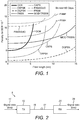
- Figure 1 shows a graph of sensitivity penalty (with respect to OOK) versus fiber length (for a chromatic dispersion coefficient of 15.7 ps/nm/km) for a 50 Gbit/s channel for a range of modulation/line coding formats.
- PAM4 Pulse Amplitude Modulation
- IEEE Institute of Electrical and Electronics Engineers
- At the transmitter four amplitude levels are generated by a Digital to Analog converter (DAC) and, at the receiver, the received signal is discriminated by using three thresholds.
- the spectral width is about half that of an OOK signal at the same bit rate.
- PAM4 is more resilient to chromatic dispersion than OOK over longer fiber lengths, making longer fiber lengths achievable, although it has an initial sensitivity penalty of about 6 dB.
- Figure 1 shows that fiber lengths of 10 km are hardly achievable without dispersion compensation (7.5 km of propagation in fiber lead to about 2dB of dispersion penalty).
- Other formats shown in Figure 1 are eight-level PAM (PAM8), Duobinary PAM4 (PAM4DUO), Differential Binary Phase Shift Keying (DBPSK), Differential Quadrature Phase Shift Keying (DQPSK) and Combined Amplitude-Phase Shift (CAPS).
- PAM4DUO is a format in which a duobinary code is applied to PAM4 to achieve a 7 level signal.
- DBPSK two levels are generated at the transmitter, for example by means of a Mach Zehnder Modulator (MZM), the two levels having same amplitude but opposite phases.
- MZM Mach Zehnder Modulator
- the transmitted information can be recovered at the receiver by an interferometer, whose arms are delayed each other by a symbol time, placed in front of a balanced photodiode.
- DBPSK behaves like OOK (the transmission is binary for both) but with a better back-to-back performance.
- Combined Amplitude-Phase Shift (CAPS) can be obtained by narrow filtering a DBPSK signal.
- DQPSK presents the best absolute performance, with the same symbol rate as PAM4 and the distance between adjacent symbols in the constellation is the same as DBPSK.
- complexity is increased, as an In-phase and Quadrature (IQ) modulator is needed at the transmitter, and the receiver requires two interferometers and two balanced photodiodes.
- IQ In-phase and Quadrature
- US 2005/0099325 A1 discloses a technique for improving the quality of digital signals in a multi-level signaling system is disclosed.
- the technique may be realized as a method for improving the quality of transmitted digital signals in a multi-level signaling system wherein digital signals representing more than one bit of information may be transmitted at more than two signal levels on a single transmission medium.
- Kaneko et al “Feedback Balanced Code for Multilevel PCM Transmisison", Electronics and Communications in Japan, Scripta Technica, vol. 52A, no. 1, 01.01.1969, pages 25-34, XPOOO760053 , discloses a novel family of optical line codes to counteract the effects of a dispersive fiber.
- An aspect of the disclosure provides a method of line coding for optical transmission.
- the method comprises encoding digital data to a set of five line symbols.
- the line symbols have amplitude values of 0, ⁇ A1, ⁇ A2, where
- At least one example of the present invention has an advantage of relatively simple receiver requirements, as the receiver can determine digital data values using a pair of amplitude thresholds.
- the complexity (and cost) is similar to PAM4.
- At least one example of the present invention has an advantage of requiring about half the optical power of PAM4, and a better tolerance to fiber chromatic dispersion than PAM4.
- the mapped line symbol depends on a current state of operation of the line coding.
- the current state of operation of the line coding is changed by the first binary value or the second binary value.
- the encoding comprises using a state machine with four states, where digital data with the first binary value causes the state machine to remain in the same state.
- the encoding comprises using a state machine, where digital data with the second binary value causes the state machine to change from state k to state k+1.
- the encoding comprises using a state machine with four states arranged in a sequence, wherein:
- An aspect of the disclosure provides a method of optical transmission.
- the method comprises encoding digital data according to the method of any example to produce an encoded signal; and modulating an optical carrier using the encoded signal.
- the modulating uses a Mach Zehnder Modulator.
- An aspect of the disclosure provides a method of receiving an optical signal in which digital data has been encoded to a set of five line symbols.
- the line symbols have amplitude values of 0, ⁇ A1, ⁇ A2, where
- the method comprising photodetecting the received signal to generate an electrical signal which can represent a set of three possible received symbols; and recovering the digital data from the received symbols.
- the method comprises recovering the digital data by comparing the electrical signal with a first amplitude threshold and a second amplitude threshold.
- recovering the digital data from the received symbols comprises determining that the digital data is a first binary value when the electrical signal is less than the first amplitude threshold or above a second amplitude threshold; and determining that the electrical signal is a second binary value when the electrical signal is between the first amplitude threshold and the second amplitude threshold.
- An aspect of the disclosure provides a line encoding apparatus for encoding a signal for optical transmission.
- the apparatus is configured to encode digital data to five line symbols.
- the line symbols have amplitude values of 0, ⁇ A1, ⁇ A2, where
- the mapped line symbol depends on a current state of operation of the line coding.
- the line encoding apparatus is configured to change a current state of operation of the line coding on receiving the first binary value or the second binary value.
- the line encoding apparatus is configured to encode as a state machine with four states, where digital data with the first binary value causes the state machine to remain in the same state.
- the encoding comprises using a state machine, where digital data with the second binary value causes the state machine to change from state k to state k+1.
- An aspect of the disclosure provides a line encoding apparatus according to any example, which is configured to perform the method of any example.
- An aspect of the disclosure provides an optical transmitter comprising a line encoding apparatus according to any example. which is configured to output an encoded signal.
- the transmitter further comprises an optical modulator which is configured to modulate an optical carrier using the encoded signal to output a modulated optical carrier.
- An aspect of the disclosure provides an optical receiver comprising a photodetection stage which is configured to receive an optical signal and to output an electrical signal.
- the optical signal carries digital data which has been encoded to a set of five line symbols.
- the line symbols have amplitude values of zero, ⁇ A1, ⁇ A2, where
- the receiver comprises a digital data recovery stage which is configured to recover the digital data from the received symbols.
- the optical receiver is configured to recover the digital data by comparing the electrical signal with a first amplitude threshold and a second amplitude threshold.
- the digital data recovery stage is configured to determine that the digital data is a first binary value when the electrical signal is less than the first amplitude threshold or above the second threshold; and determine that the electrical signal is a second binary value when the electrical signal is between the first amplitude threshold and the second amplitude threshold.
- An aspect of the disclosure provides a line encoding apparatus for encoding a signal for optical transmission.
- the apparatus comprising a receiving unit configured to receive digital data; and a state unit configured to determine an operational state of the line encoding apparatus.
- the apparatus further comprises an encoding unit configured to map the received digital data to five line symbols.
- the line symbols have amplitude values of 0, ⁇ A1, ⁇ A2, where
- An aspect of the disclosure provides a line encoding apparatus for encoding a signal for optical transmission.
- the line encoding apparatus comprising processing circuitry, the processing circuitry being configured to cause the line encoding apparatus to encode digital data to a set of five line symbols.
- the line symbols have amplitude values of 0, ⁇ A1, ⁇ A2, where
- An aspect of the disclosure provides a computer program for encoding a signal for optical transmission.
- the computer program comprising computer code which, when run on processing circuitry of a line encoding apparatus, causes the line encoding apparatus to encode digital data to a set of five line symbols.
- the line symbols have amplitude values of 0, ⁇ A1, ⁇ A2, where
- An aspect of the disclosure provides a computer program product comprising a computer program according to an example, and a computer readable storage medium on which the computer program is stored.
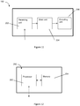
- Figure 2 shows an example of an optical transmission system 5 comprising an optical transmitter 10 and an optical receiver 20 connected by an optical fiber 17.
- the optical transmission system 5 can form part of an access network, an aggregation network or some other communications network.
- the optical transmitter 10 receives digital data 11 and outputs an optical signal 16 which is line coded and modulated with the digital data.
- the optical receiver 20 receives the optical signal 16, retrieves the digital data, and outputs the digital data 26.
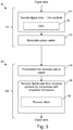
- FIG 3 shows an overview of a method performed by the optical transmitter 10 and the optical receiver 20.
- the transmitter 10 receives binary digital data and, at block 31, encodes the digital data to a set of line symbols. There is a set of five line symbols.
- the line symbols have the amplitude values: 0, ⁇ A1, ⁇ A2, where
- the line symbols are ⁇ -A2, -A1, 0, +A1, +A2 ⁇ .
- a first binary value (e.g. a binary '0') maps to the line symbols 0 and ⁇ A2.
- a second binary value (e.g. a binary '1') maps to the line symbols ⁇ A1.
- the encoding process outputs a multi-level signal.
- the encoding process may use digital-to-analog conversion 32 to generate the multi-level signal.
- an optical carrier is modulated with the multi-level signal.
- the encoding process at block 31 can map binary data directly to the set of line symbol values ⁇ -A2, -A1, 0, A1, A2 ⁇ of the modulated optical signal. If a modulator with a non-linear input-output relationship (transfer function) is used at block 33, the encoding process at block 31 can map binary data to a set of intermediate values which, when applied to the non-linear modulator at block 33, correspond to the set of line symbol values ⁇ -A2, -A1, 0, A1, A2 ⁇ .
- transfer function transfer function
- the encoding process maps binary data to a set of values which gives those inputs.
- the receiver 20 receives the modulated optical signal.
- the receiver performs photodetection of the received optical signal. That is, the receiver converts the optical signal to an electrical signal.
- the receiver recovers digital data from the received symbols. This block uses amplitude thresholds. The electrical signal is compared with thresholds to determine the original digital data binary value corresponding to the electrical signal.
- the receiver may determine a clock from the received signal for use in decoding digital data. The clock can be used to determine the times at which the received signal is compared with the thresholds TH1, TH2.
- Figure 4 shows signals at different stages of the transmission.
- Binary digital data 11 having values of '0' and '1' is encoded to one of a set of five line symbols.
- the five line symbols have values of one of: -A2, -A1, 0, +A1, +A2.
- An example line signal 16 generated from the line symbols is shown, e.g. by smoothing or a further operation.
- the line encoded signal transitions between the set of five line symbols.
- the line encoding maps a first binary value (e.g. binary '0') to the line symbols 0 and ⁇ A2.
- the line encoding maps a second binary value (e.g. binary '1') to the line symbols ⁇ A1.
- Signal 14 is a multi-level signal output or generated by the encoder. As for conventional OOK binary signals, the signal 14 may be low-pass filtered to smooth the transitions between the line symbols. An optical carrier is modulated using the signal 14, or a low-pass filtered version of signal 14. Figure 4 assumes the modulator is linear. If a non-linear modulator is used, the multi-level signal 14 has a set of values which, when applied to the non-linear modulator, correspond to the set of line symbol values ⁇ - ⁇ 2, -1, 0, +1, + ⁇ 2 ⁇ .
- Figure 4 shows an eye diagram 22 of the optical signal, after photo-detection.
- the five line symbols of the transmitted signal : -A2, -A1, 0, +A1, +A2 correspond to three received symbols: RS1, RS2, RS3.
- the relationship between line symbols, received symbols and binary data values is:
- the relationship between line symbols and received symbols is due to the photo-detection process, which considers optical intensity (power) of the received signal.
- the photo-detector outputs a current proportional to the input optical power, which is the square of the absolute value of the input electrical field in the optical fiber. Therefore, the line symbols +A1 and -A1, after photo-detection, correspond to the same received symbol RS2, and the line symbols +A2 and -A2, after photodetection, correspond to the same received symbol RS3.
- three symbols are detected.
- the thresholds are set mid-way between the expected values of the received symbols RS1, RS2, RS3.
- a received signal is determined to be a binary 1 if the sampled signal falls in the range 0.5 ⁇ x ⁇ 1.5, and a binary 0 if 0 ⁇ x ⁇ 0.5, or if 1.5 ⁇ x ⁇ 2.0.
- Figure 5 shows a state machine 40 which is used to map binary digital data to a set of line symbols.
- the data maps to a line symbol according to a current state of the state machine.
- the line encoding apparatus may be considered as operating as a state machine.
- the line encoding apparatus may be considered as operating in one of the states of the state machine 40 to generate a line symbol value from the input digital data, the selected line symbol value depending on the current operating state.
- the upper part of Figure 5 shows a set of signal transitions: s1 (t), s2(t), s3(t).
- the state machine 40 has four states: ⁇ 1, ⁇ 2, ⁇ 3, ⁇ 4 arranged in a continuous sequence.
- the state machine operates on a bit-by-bit basis.
- the signal transitions: s1(t), s2(t), s3(t) are shown with amplitude values 0, A1, A2.
- the set of values is modified to values which, when applied to the non-linear modulator, correspond to the set of line symbol values ⁇ -A2, -A1, 0, +A1, +A2 ⁇ .
- the operating state of the state machine is changed by one of the input data values.
- the line encoding apparatus is configured to change a current state of operation of the line coding on receiving the first binary value or the second binary value.
- the operating state of the state machine is not changed by the other of the input data values.
- binary digital data with the first binary value e.g. binary '0'
- binary digital data with the second binary value e.g. binary '1'
- the state machine cycles around the discrete number of operating states (e.g. four).
- an advance of the state causes the state machine to change from state k to state k+1 mod(4).
- the state machine is symmetrical. That is, the pattern of states, and of operations of the state machine, is symmetrical about lines 41 and 42.
- the amplitude values of the line symbols mapped when changing state from state 4 to state 1 and from state 1 to state 2 are equal.
- the amplitude values of the line symbols mapped when changing state from state 2 to state 3 and from state 3 to state 4 are equal, and opposite to the amplitude values of the line symbols mapped when changing state from state 4 to state 1 and from state 1 to state 2.
- the mapped line symbol depends on a current state of operation of the line coding.
- the current state of operation of the line coding is changed by the first binary value or the second binary value.
- the mapped line symbol depends on a current state of the line coding.
- the state of the line coding (i.e. on the state machine) is changed by one or more values of the data which is being mapped to the line symbols.
- References to implementation by a state machine may indicate an encoder, transmitter or line encoding apparatus configured to operate according to a state machine, i.e. output depends on a current operational state.
- Binary digital data with the other of the values e.g. second binary value (e.g. binary 1) causes the state machine to move to the next state, where:
- the determined line symbol (e.g. one of the set ⁇ -A2, -A1, 0, +A1, +A2 ⁇ ) is based on both the input binary value (e.g. 0 or 1) and the current state of operation of the encoder or method, e.g. in state 1,2,3 or 4.
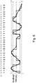
- Figure 6 shows the sequence of states (labelled as states ⁇ 1, ⁇ 2, ⁇ 3, ⁇ 4) corresponding to a sequence of binary digital data (e.g. 1 1 0 1 1 1 0).
- the state machine begins in state ⁇ 1.
- the next binary data 0 and the state machine performs a transition s1(t) to a line symbol with amplitude +A2 and remains in state 3.
- the process continues through the sequence of states and transitions between line symbols as shown in Figure 6 .
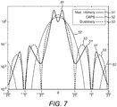
- Figure 7 shows the spectrum of the transmitted signal 51 according to an example of the disclosure, plotted as power spectral density against frequency, where T is the duration of a bit period of the transmitted signal. Spectra of a CAP signal 52 and a duobinary signal 53 are also shown for comparison. It can be seen that the transmitted signal 51 has enhanced energy concentration around the lowest frequencies.
- Figure 8 shows apparatus at an optical transmitter 10 and an optical receiver 20.
- the optical transmitter 10 has an input to receive digital data.
- the optical transmitter 10 comprises an encoder 12 (also referred to as a line encoding apparatus) which maps binary digital data to line symbols.
- the encoder 12 can comprise, or be considered to operate as, a state machine 40 as previously described.
- the encoder 12 may directly output analog signals at amplitudes corresponding to the set of line symbols (i.e. -A2, -A1, 0, +A1, +A2).
- the encoder 12 is for encoding a signal for transmission, e.g. optical transmission.
- the encoder 12 may indicate, for each operation of the state machine, a line symbol required.
- each of the five line symbols can correspond to a digital code which is used internally by the transmitter.
- a digital-to-analog converter (DAC) 13 outputs an analog value, corresponding to the digital code of the required line symbol.
- the output of the encoder, or DAC 13 (if used), is a multi-level analog signal 14 (e.g. 14, Figure 4 ).
- a low pass filter may be included in the transmitter 10 to low pass filter the signal.
- a low-pass filtering effect is provided by the limited bandwidth of the modulator.
- the analog signal is used to modulate an optical carrier in an optical modulation stage 15 (e.g. Mach Zehnder Modulator) and output a modulated optical signal 16.
- an optical modulation stage 15 e.g. Mach Zehnder Modulator
- the receiver 20 has an input to receive a modulated optical signal 16.
- the receiver 20 comprises a photodetection stage 21 which is configured to receive an optical signal and to output an electrical signal 22. As described above, the photodetection stage 21 outputs an electrical signal which is proportional to power of the received optical signal.
- the photodetection stage may include an electrical amplifier (e.g. a transimpedance amplifier).
- the electrical signal can represent a set of three possible received symbols.
- a digital data recovery stage 23 is configured to recover digital data from the received symbols.
- the digital data recovery stage 23 comprises a threshold decision unit 25 which is configured to compare the electrical signal with a first amplitude threshold TH1 and a second amplitude threshold TH2. This can operate as shown in the lower part of Figure 4 .
- the digital data recovery stage 23 can also comprise a clock extraction and sampling unit 24 which is configured to extract a clock signal from the detected electrical signal and to sample the detected electrical signal at points in time determined by the extracted clock.
- the threshold decision unit 25 is configured to determine that the digital data is a first binary value when the electrical signal 22 is less than the first amplitude threshold TH1 or above the second amplitude threshold TH2.
- the threshold decision unit 25 is configured to determine that the electrical signal is a second binary value when the electrical signal is between the first amplitude threshold TH1 and the second amplitude threshold TH2.
- the determined symbol value is output as digital data 26, corresponding to the transmitted digital data 11.
- a modified tribinary (MOD-TRIBIN) signal of the type described above is shown alongside other signal formats in the graph of sensitivity penalty (with respect to OOK) versus fiber length (for a chromatic dispersion coefficient of 15.7 ps/nm/km) for a 50 Gbit/s channel for a range of modulation/line coding formats.
- the modified tribinary (MOD-TRIBIN) signal is comparable in complexity to PAM4 while its back-to-back performance is 3 dB better.
- the modified tribinary signal behaves like a DQPSK signal over a range of fiber lengths.
- FIG 9 shows a Mach Zehnder Modulator (MZM) 60 which can be used in the optical modulation stage 15 of the optical transmitter 10 of Figure 8 .
- the MZM 60 has an input port 61 and an output port 62.
- Optical radiation from a suitable source e.g. a laser
- the MZM has two waveguides 65, 66, called arms.
- a splitter 63 connects the input 61 to the two arms 65, 66.
- a combiner 64 connects the two arms 65, 66 to the output 62.
- a out ⁇ 2 * cos ⁇ / 2 * V / V ⁇
- Figure 10 shows a plot of the MZM transfer function, showing electrical field in the optical fiber (A out ) against normalised voltage V/V ⁇ .
- This is an example of a modulator with a non-linear input-output transfer function. The values are normalized to the square root of the transmitted optical power.
- the relationship between inputs and outputs shown in Figure 10 is one possible example. Other relationships are possible by use of a bias voltage at the MZM.
- the bias voltage has the effect of shifting the MZM transfer function along the x-axis in Figure 10 .
- the processing apparatus can comprise a computer, a processor, a state machine, a logic array or any other suitable processing apparatus.
- the processing apparatus can be a general-purpose processor which executes software to cause the general-purpose processor to perform the required tasks, or the processing apparatus can be dedicated to perform the required functions.
- Another aspect of the invention provides machine-readable instructions (software) which, when executed by a processor, perform any of the described methods.
- the machine-readable instructions may be stored on an electronic memory device, hard disk, optical disk or other machine-readable storage medium.
- the machine-readable medium can be a non-transitory machine-readable medium.
- the term "non-transitory machine-readable medium" comprises all machine-readable media except for a transitory, propagating signal.
- the machine-readable instructions can be downloaded to the storage medium via a network connection.
- Figure 11 shows an example of a line encoding apparatus, transmitter or encoder 150, corresponding to the encoder 12.
- a receiving unit 202 is configured to receive the digital data.
- a state unit 204 is configured to determine a state of the encoder, i.e. a state of operation of the encoder operating as a state machine.
- An encoding unit 206 is configured to receive the state and the digital data to be encoded. The encoding unit 206 determines the symbol value according to the method and values as described above.
- the units or modules described may be implemented in software, firmware or hardware. A description of a separate unit does not indicate a separate implementation, one or more units may be implemented by the same software, firmware or hardware.
- Figure 12 shows a further example of a line encoding apparatus, transmitter or encoder 250 providing the line encoding apparatus or encoder 12.
- the control entity 250 comprises a processor or processing circuitry 252 and a memory or storage medium 254.
- the memory contains instructions executable by the processor, whereby the control entity is operative to implement the method described in any example.
- the memory contains instructions executable by the processor, whereby the control entity is operative to implement any example of the disclosure.
- the receiving unit 202, state unit 204 and the encoding unit 206 described above are implemented as a computer program running on the processor 252.
- the computer program is for encoding a signal for optical transmission.
- the computer program comprising computer code which, when run on processing circuitry 252 of a line encoding apparatus, causes the line encoding apparatus to encode 31 digital data to a set of five line symbols; where the line symbols have amplitude values of 0, ⁇ A1, ⁇ A2, where
- the computer program is arranged to carry out the functions of any example.
- the processor or processing circuitry is provided using any combination of one or more of a suitable central processing unit (CPU), multiprocessor, microcontroller, digital signal processor (DSP), etc., capable of executing software instructions stored in a computer program product, e.g. in the form of the storage medium 254.
- the processing circuitry may further be provided as at least one application specific integrated circuit (ASIC), or field programmable gate array (FPGA).
- ASIC application specific integrated circuit
- FPGA field programmable gate array
- the processing circuitry 252 is configured to cause the line encoding apparatus to perform a set of operations as disclosed above.
- the storage medium 254 may store the set of operations
- the processing circuitry 252 may be configured to retrieve the set of operations from the storage medium 254 to cause the line encoding apparatus 250 to perform the set of operations.
- the set of operations may be provided as a set of executable instructions.
- the processing circuitry 252 is thereby arranged to execute methods as herein disclosed.
- the storage medium 254 may also comprise persistent storage, which, for example, can be any single one or combination of magnetic memory, optical memory, solid state memory or even remotely mounted memory.
- the processing circuitry 252 includes or is connected to the DAC 13, and may be functionally connected to the optical modulation stage 15.
- Examples of the disclosure have been described as relating to optical transmission or optical receiving. Alternatively, the examples may also be considered to relate to electrical transmission or receiving.
- the line symbol values and state machine operation are also suitable for generation of symbols for electrical transmission.
Landscapes
- Physics & Mathematics (AREA)
- Nonlinear Science (AREA)
- Engineering & Computer Science (AREA)
- Computer Networks & Wireless Communication (AREA)
- Signal Processing (AREA)
- Optics & Photonics (AREA)
- Spectroscopy & Molecular Physics (AREA)
- General Physics & Mathematics (AREA)
- Electromagnetism (AREA)
- Optical Communication System (AREA)
Claims (12)
- Procédé de codage de ligne pour une transmission optique comprenant :l'encodage de données numériques en un ensemble de cinq symboles de ligne ;où les symboles de ligne ont des valeurs d'amplitude de 0, ± A1, ± A2, où |A2| > |A1|,où :une première valeur binaire se mappe aux symboles de ligne ayant des valeurs d'amplitude de 0 et ± A2 ;une deuxième valeur binaire se mappe aux symboles de ligne ayant des valeurs d'amplitude de ± A1 ;où l'encodage comprend l'utilisation d'une machine d'état avec quatre états agencés en séquence, dans lequel :
des données numériques avec la première valeur binaire amènent la machine d'état à rester dans le même état, où :dans un état 1, des données numériques avec la première valeur binaire amènent la machine d'état à mapper les données numériques à un symbole de ligne avec une amplitude -A2 ;dans un état 2, des données numériques avec la première valeur binaire amènent la machine d'état à mapper les données numériques à un symbole de ligne avec une amplitude 0 ;dans un état 3, des données numériques avec la première valeur binaire amènent la machine d'état à mapper les données numériques à un symbole de ligne avec une amplitude +A2 ;dans un état 4, des données numériques avec la première valeur binaire amènent la machine d'état à mapper les données numériques à un symbole de ligne avec une amplitude 0 ;des données numériques avec la deuxième valeur binaire amènent la machine d'état à passer à l'état suivant, où :dans l'état 1, des données numériques avec la deuxième valeur binaire amènent la machine d'état à mapper les données numériques à un symbole de ligne avec une amplitude -A1 ;dans l'état 2, des données numériques avec la deuxième valeur binaire amènent la machine d'état à mapper les données numériques à un symbole de ligne avec une amplitude +A1 ;dans l'état 3, des données numériques avec la deuxième valeur binaire amènent la machine d'état à mapper les données numériques à un symbole de ligne avec une amplitude +A1 ;dans l'état 4, des données numériques avec la deuxième valeur binaire amènent la machine d'état à mapper les données numériques à un symbole de ligne avec une amplitude -A1 ;dans lequel l'état suivant pour l'état 4 est l'état 1. - Procédé selon la revendication 1 dans lequel le symbole de ligne mappé dépend d'un état de fonctionnement actuel du codage de ligne et dans lequel l'état de fonctionnement actuel du codage de ligne est modifié par la première valeur binaire ou la deuxième valeur binaire.
- Procédé selon l'une quelconque des revendications précédentes dans lequel les valeurs d'amplitude des symboles de ligne sont dans le rapport A1:A2 = 1:√2.
- Procédé de transmission optique comprenant :l'encodage de données numériques selon le procédé de l'une quelconque des revendications 1 à 3 pour produire un signal encodé ; etla modulation d'une porteuse optique à l'aide du signal encodé.
- Procédé selon la revendication 4 dans lequel la modulation utilise un modulateur de Mach Zehnder.
- Procédé de réception d'un signal optique dans lequel des données numériques ont été encodées en un ensemble de cinq symboles de ligne, où les symboles de ligne ont des valeurs d'amplitude de 0, ± A1, ± A2, où |A2| > |A1|, où une première valeur binaire se mappe aux symboles de ligne 0 et ± A2 et une deuxième valeur binaire se mappe aux symboles de ligne ± A1, le procédé comprenant :la photodétection du signal reçu pour générer un signal électrique qui représente un ensemble de trois symboles reçus possibles ; etla récupération des données numériques à partir des symboles reçus, dans lequel la récupération des données numériques à partir des symboles reçus comprend :la détermination du fait que les données numériques sont une première valeur binaire lorsque le signal électrique est inférieur au premier seuil d'amplitude ou supérieur à un deuxième seuil d'amplitude, etla détermination du fait que le signal électrique est une deuxième valeur binaire lorsque le signal électrique est entre le premier seuil d'amplitude et le deuxième seuil d'amplitude.
- Appareil de codage de ligne pour encoder un signal pour une transmission optique, l'appareil comprenant :une unité de réception (202) configurée pour recevoir des données numériques ;une unité d'état (204) configurée pour déterminer un état fonctionnel de l'appareil d'encodage de ligne, etune unité d'encodage (206) configurée pour mapper les données numériques reçues à cinq symboles de ligne,où les symboles de ligne ont des valeurs d'amplitude de 0, ± A1, ± A2, où |A2| > |A1|,dans lequel l'unité d'encodage (206) est configurée pour mapper :une première valeur binaire aux symboles de ligne ayant des valeurs d'amplitude de 0 et ± A2 ;une deuxième valeur binaire aux symboles de ligne ayant des valeurs d'amplitude de ± A1 ;où l'encodage comprend l'utilisation d'une machine d'état avec quatre états agencés en séquence, dans lequel :
des données numériques avec la première valeur binaire amènent la machine d'état à rester dans le même état, où :dans un état 1, des données numériques avec la première valeur binaire amènent la machine d'état à mapper les données numériques à un symbole de ligne avec une amplitude -A2 ;dans un état 2, des données numériques avec la première valeur binaire amènent la machine d'état à mapper les données numériques à un symbole de ligne avec une amplitude 0 ;dans un état 3, des données numériques avec la première valeur binaire amènent la machine d'état à mapper les données numériques à un symbole de ligne avec une amplitude +A2 ;dans un état 4, des données numériques avec la première valeur binaire amènent la machine d'état à mapper les données numériques à un symbole de ligne avec une amplitude 0 ;des données numériques avec la deuxième valeur binaire amènent la machine d'état à passer à l'état suivant, où :dans l'état 1, des données numériques avec la deuxième valeur binaire amènent la machine d'état à mapper les données numériques à un symbole de ligne avec une amplitude -A1 ;dans l'état 2, des données numériques avec la deuxième valeur binaire amènent la machine d'état à mapper les données numériques à un symbole de ligne avec une amplitude +A1 ;dans l'état 3, des données numériques avec la deuxième valeur binaire amènent la machine d'état à mapper les données numériques à un symbole de ligne avec une amplitude +A1 ;dans l'état 4, des données numériques avec la deuxième valeur binaire amènent la machine d'état à mapper les données numériques à un symbole de ligne avec une amplitude -A1 ;dans lequel l'état suivant pour l'état 4 est l'état 1. - Appareil de codage de ligne selon la revendication 7 dans lequel le symbole de ligne mappé dépend d'un état de fonctionnement actuel du codage de ligne.
- Appareil de codage de ligne selon la revendication 7 ou 8 dans lequel l'appareil de codage de ligne est configuré pour modifier un état de fonctionnement actuel du codage de ligne à la réception de la première valeur binaire ou de la deuxième valeur binaire.
- Émetteur optique comprenant :
un appareil d'encodage de ligne selon les revendications 7 à 9 qui est configuré pour fournir en sortie un signal encodé ; et un modulateur optique qui est configuré pour moduler une porteuse optique à l'aide du signal encodé pour fournir en sortie une porteuse optique modulée. - Récepteur optique comprenant :un étage de photodétection qui est configuré pour recevoir un signal optique et pour fournir en sortie un signal électrique, dans lequel le signal optique est porteur de données numériques qui ont été encodées en un ensemble de cinq symboles de ligne, où les symboles de ligne ont des valeurs d'amplitude de zéro, ± A1, ± A2, où |A2| > |A1|, où une première valeur binaire est mappée aux symboles de ligne 0 et ± A2 et une deuxième valeur binaire est mappée aux symboles de ligne ± A1, et où le signal électrique représente un ensemble de trois symboles reçus possible ; etun étage de récupération de données numériques qui est configuré pour récupérer les données numériques à partir des symboles reçus, dans lequel le récepteur optique est configuré pour récupérer les données numériques en comparant le signal électrique à un premier seuil d'amplitude et un deuxième seuil d'amplitude, etdans lequel l'étage de récupération de données numériques est configuré pour :déterminer que les données numériques sont une première valeur binaire lorsque le signal électrique est inférieur au premier seuil d'amplitude ou supérieur au deuxième seuil d'amplitude, etdéterminer que le signal électrique est une deuxième valeur binaire lorsque le signal électrique est entre le premier seuil d'amplitude et le deuxième seuil d'amplitude.
- Programme informatique pour encoder un signal pour une transmission optique, le programme informatique comprenant un code informatique qui, lorsqu'il est exécuté qu'une circuiterie de traitement d'un appareil d'encodage de ligne, amène l'appareil d'encodage de ligné à :encoder des données numériques en un ensemble de cinq symboles de ligne ;où les symboles de ligne ont des valeurs d'amplitude de 0, ± A1, ± A2, où |A2| > |A1|,où :une première valeur binaire se mappe aux symboles de ligne ayant des valeurs d'amplitude de 0 et ± A2 ;une deuxième valeur binaire se mappe aux symboles de ligne ayant des valeurs d'amplitude de ± A1 ;où l'encodage comprend l'utilisation d'une machine d'état avec quatre états agencés en séquence, dans lequel :
des données numériques avec la première valeur binaire amènent la machine d'état à rester dans le même état, où :dans un état 1, des données numériques avec la première valeur binaire amènent la machine d'état à mapper les données numériques à un symbole de ligne avec une amplitude -A2 ;dans un état 2, des données numériques avec la première valeur binaire amènent la machine d'état à mapper les données numériques à un symbole de ligne avec une amplitude 0 ;dans un état 3, des données numériques avec la première valeur binaire amènent la machine d'état à mapper les données numériques à un symbole de ligne avec une amplitude +A2 ;dans un état 4, des données numériques avec la première valeur binaire amènent la machine d'état à mapper les données numériques à un symbole de ligne avec une amplitude 0 ;des données numériques avec la deuxième valeur binaire amènent la machine d'état à passer à l'état suivant, où :dans l'état 1, des données numériques avec la deuxième valeur binaire amènent la machine d'état à mapper les données numériques à un symbole de ligne avec une amplitude -A1 ;dans l'état 2, des données numériques avec la deuxième valeur binaire amènent la machine d'état à mapper les données numériques à un symbole de ligne avec une amplitude +A1 ;dans l'état 3, des données numériques avec la deuxième valeur binaire amènent la machine d'état à mapper les données numériques à un symbole de ligne avec une amplitude +A1 ;dans l'état 4, des données numériques avec la deuxième valeur binaire amènent la machine d'état à mapper les données numériques à un symbole de ligne avec une amplitude -A1 ;dans lequel l'état suivant pour l'état 4 est l'état 1.
Applications Claiming Priority (1)
| Application Number | Priority Date | Filing Date | Title |
|---|---|---|---|
| PCT/EP2016/061827 WO2017202464A1 (fr) | 2016-05-25 | 2016-05-25 | Codage de ligne pour transmission optique |
Publications (2)
| Publication Number | Publication Date |
|---|---|
| EP3466005A1 EP3466005A1 (fr) | 2019-04-10 |
| EP3466005B1 true EP3466005B1 (fr) | 2021-07-07 |
Family
ID=56087258
Family Applications (1)
| Application Number | Title | Priority Date | Filing Date |
|---|---|---|---|
| EP16725836.7A Active EP3466005B1 (fr) | 2016-05-25 | 2016-05-25 | Codage de ligne pour transmission optique |
Country Status (3)
| Country | Link |
|---|---|
| US (1) | US10895797B2 (fr) |
| EP (1) | EP3466005B1 (fr) |
| WO (1) | WO2017202464A1 (fr) |
Families Citing this family (7)
| Publication number | Priority date | Publication date | Assignee | Title |
|---|---|---|---|---|
| WO2018028784A1 (fr) | 2016-08-10 | 2018-02-15 | Telefonaktiebolaget Lm Ericsson (Publ) | Codage destiné à une transmission optique |
| CN109565487B (zh) * | 2016-08-31 | 2020-10-16 | 华为技术有限公司 | 一种信号调制和解调的方法、装置及系统 |
| WO2019185143A1 (fr) | 2018-03-28 | 2019-10-03 | Telefonaktiebolaget Lm Ericsson (Publ) | Procédé et appareil de caractérisation d'un environnement à radiofréquences dans un réseau de télécommunications |
| US11886055B2 (en) | 2019-12-22 | 2024-01-30 | Mellanox Technologies, Ltd. | Low voltage modulator |
| US11630369B2 (en) * | 2021-07-19 | 2023-04-18 | Mellanox Technologies, Ltd. | Generation of an optical PAM-4 signal in a Mach-Zehnder modulator |
| US11855700B2 (en) | 2021-12-16 | 2023-12-26 | Mellanox Technologies, Ltd. | High bandwidth optical modulator |
| US11906873B2 (en) | 2022-01-05 | 2024-02-20 | Mellanox Technologies, Ltd. | Serial data conversion redundancy using optical modulators |
Family Cites Families (3)
| Publication number | Priority date | Publication date | Assignee | Title |
|---|---|---|---|---|
| US6490069B1 (en) | 2001-01-29 | 2002-12-03 | Stratalight Communications, Inc. | Transmission and reception of duobinary multilevel pulse-amplitude-modulated optical signals using subtraction-based encoder |
| US7620116B2 (en) * | 2003-02-28 | 2009-11-17 | Rambus Inc. | Technique for determining an optimal transition-limiting code for use in a multi-level signaling system |
| US6917312B2 (en) | 2003-11-10 | 2005-07-12 | Rambus Inc. | Technique for improving the quality of digital signals in a multi-level signaling system |
-
2016
- 2016-05-25 WO PCT/EP2016/061827 patent/WO2017202464A1/fr unknown
- 2016-05-25 US US16/302,016 patent/US10895797B2/en active Active
- 2016-05-25 EP EP16725836.7A patent/EP3466005B1/fr active Active
Also Published As
| Publication number | Publication date |
|---|---|
| US20190146303A1 (en) | 2019-05-16 |
| WO2017202464A1 (fr) | 2017-11-30 |
| EP3466005A1 (fr) | 2019-04-10 |
| US10895797B2 (en) | 2021-01-19 |
Similar Documents
| Publication | Publication Date | Title |
|---|---|---|
| EP3466005B1 (fr) | Codage de ligne pour transmission optique | |
| US7546041B2 (en) | Optical communications | |
| Ohm et al. | Quaternary optical ASK-DPSK and receivers with direct detection | |
| CN101895495B (zh) | 正交双偏振差分四相相移键控发射与接收的方法及其系统 | |
| EP2154796B1 (fr) | Équipement de réception, procédé de modulation de signal par déplacement de phase en quadrature différentielle et procédé d'obtention | |
| EP2206306B1 (fr) | Transmission binaire à forme de phase équilibrée dans des communications optiques | |
| US7327961B2 (en) | Differential encoder for an optical DQPSK modulator | |
| WO2016051410A1 (fr) | Conversion de constellation photonique au silicium entièrement optique de formats de modulation d'amplitude et de phase | |
| US7941058B2 (en) | Device and method for decoding an optical multi-level DPSK signal | |
| US20110006825A1 (en) | Phase Control Circuit and Method for Optical Receivers | |
| CN100501505C (zh) | 直接光学n状态相移键控 | |
| US8687970B2 (en) | Modulator and demodulator for a differential optical modulation format with eight phase changes | |
| EP1633061B1 (fr) | Système et procédé pour augmenter l'efficacité spectrale d'un signal digital en code binaire | |
| EP3497825B1 (fr) | Codage destiné à une transmission optique | |
| Elsherif et al. | Performance enhancement of mapping multiplexing technique utilising dual‐drive Mach–Zehnder modulator for metropolitan area networks | |
| Malekmohammadi et al. | Analysis of return-to-zero-on-off-keying over absolute polar duty cycle division multiplexing in dispersive transmission medium | |
| Shao et al. | 8PSK Signals with 50% RZ Clock for Optical Access System Applications Using Phase Equalization Technique in MSPE | |
| Rozorynov et al. | Development of modulation formats in optical fiber communication channel |
Legal Events
| Date | Code | Title | Description |
|---|---|---|---|
| STAA | Information on the status of an ep patent application or granted ep patent |
Free format text: STATUS: UNKNOWN |
|
| STAA | Information on the status of an ep patent application or granted ep patent |
Free format text: STATUS: THE INTERNATIONAL PUBLICATION HAS BEEN MADE |
|
| PUAI | Public reference made under article 153(3) epc to a published international application that has entered the european phase |
Free format text: ORIGINAL CODE: 0009012 |
|
| STAA | Information on the status of an ep patent application or granted ep patent |
Free format text: STATUS: REQUEST FOR EXAMINATION WAS MADE |
|
| 17P | Request for examination filed |
Effective date: 20181211 |
|
| AK | Designated contracting states |
Kind code of ref document: A1 Designated state(s): AL AT BE BG CH CY CZ DE DK EE ES FI FR GB GR HR HU IE IS IT LI LT LU LV MC MK MT NL NO PL PT RO RS SE SI SK SM TR |
|
| AX | Request for extension of the european patent |
Extension state: BA ME |
|
| STAA | Information on the status of an ep patent application or granted ep patent |
Free format text: STATUS: REQUEST FOR EXAMINATION WAS MADE |
|
| DAV | Request for validation of the european patent (deleted) | ||
| DAX | Request for extension of the european patent (deleted) | ||
| GRAP | Despatch of communication of intention to grant a patent |
Free format text: ORIGINAL CODE: EPIDOSNIGR1 |
|
| STAA | Information on the status of an ep patent application or granted ep patent |
Free format text: STATUS: GRANT OF PATENT IS INTENDED |
|
| INTG | Intention to grant announced |
Effective date: 20210318 |
|
| RIN1 | Information on inventor provided before grant (corrected) |
Inventor name: CAVALIERE, FABIO Inventor name: FORESTIERI, ENRICO |
|
| GRAS | Grant fee paid |
Free format text: ORIGINAL CODE: EPIDOSNIGR3 |
|
| GRAA | (expected) grant |
Free format text: ORIGINAL CODE: 0009210 |
|
| STAA | Information on the status of an ep patent application or granted ep patent |
Free format text: STATUS: THE PATENT HAS BEEN GRANTED |
|
| AK | Designated contracting states |
Kind code of ref document: B1 Designated state(s): AL AT BE BG CH CY CZ DE DK EE ES FI FR GB GR HR HU IE IS IT LI LT LU LV MC MK MT NL NO PL PT RO RS SE SI SK SM TR |
|
| REG | Reference to a national code |
Ref country code: GB Ref legal event code: FG4D |
|
| REG | Reference to a national code |
Ref country code: AT Ref legal event code: REF Ref document number: 1409690 Country of ref document: AT Kind code of ref document: T Effective date: 20210715 |
|
| REG | Reference to a national code |
Ref country code: DE Ref legal event code: R096 Ref document number: 602016060299 Country of ref document: DE |
|
| REG | Reference to a national code |
Ref country code: IE Ref legal event code: FG4D |
|
| REG | Reference to a national code |
Ref country code: LT Ref legal event code: MG9D |
|
| REG | Reference to a national code |
Ref country code: NL Ref legal event code: MP Effective date: 20210707 |
|
| REG | Reference to a national code |
Ref country code: AT Ref legal event code: MK05 Ref document number: 1409690 Country of ref document: AT Kind code of ref document: T Effective date: 20210707 |
|
| PG25 | Lapsed in a contracting state [announced via postgrant information from national office to epo] |
Ref country code: RS Free format text: LAPSE BECAUSE OF FAILURE TO SUBMIT A TRANSLATION OF THE DESCRIPTION OR TO PAY THE FEE WITHIN THE PRESCRIBED TIME-LIMIT Effective date: 20210707 Ref country code: SE Free format text: LAPSE BECAUSE OF FAILURE TO SUBMIT A TRANSLATION OF THE DESCRIPTION OR TO PAY THE FEE WITHIN THE PRESCRIBED TIME-LIMIT Effective date: 20210707 Ref country code: PT Free format text: LAPSE BECAUSE OF FAILURE TO SUBMIT A TRANSLATION OF THE DESCRIPTION OR TO PAY THE FEE WITHIN THE PRESCRIBED TIME-LIMIT Effective date: 20211108 Ref country code: NL Free format text: LAPSE BECAUSE OF FAILURE TO SUBMIT A TRANSLATION OF THE DESCRIPTION OR TO PAY THE FEE WITHIN THE PRESCRIBED TIME-LIMIT Effective date: 20210707 Ref country code: NO Free format text: LAPSE BECAUSE OF FAILURE TO SUBMIT A TRANSLATION OF THE DESCRIPTION OR TO PAY THE FEE WITHIN THE PRESCRIBED TIME-LIMIT Effective date: 20211007 Ref country code: HR Free format text: LAPSE BECAUSE OF FAILURE TO SUBMIT A TRANSLATION OF THE DESCRIPTION OR TO PAY THE FEE WITHIN THE PRESCRIBED TIME-LIMIT Effective date: 20210707 Ref country code: ES Free format text: LAPSE BECAUSE OF FAILURE TO SUBMIT A TRANSLATION OF THE DESCRIPTION OR TO PAY THE FEE WITHIN THE PRESCRIBED TIME-LIMIT Effective date: 20210707 Ref country code: FI Free format text: LAPSE BECAUSE OF FAILURE TO SUBMIT A TRANSLATION OF THE DESCRIPTION OR TO PAY THE FEE WITHIN THE PRESCRIBED TIME-LIMIT Effective date: 20210707 Ref country code: AT Free format text: LAPSE BECAUSE OF FAILURE TO SUBMIT A TRANSLATION OF THE DESCRIPTION OR TO PAY THE FEE WITHIN THE PRESCRIBED TIME-LIMIT Effective date: 20210707 Ref country code: BG Free format text: LAPSE BECAUSE OF FAILURE TO SUBMIT A TRANSLATION OF THE DESCRIPTION OR TO PAY THE FEE WITHIN THE PRESCRIBED TIME-LIMIT Effective date: 20211007 Ref country code: LT Free format text: LAPSE BECAUSE OF FAILURE TO SUBMIT A TRANSLATION OF THE DESCRIPTION OR TO PAY THE FEE WITHIN THE PRESCRIBED TIME-LIMIT Effective date: 20210707 |
|
| PG25 | Lapsed in a contracting state [announced via postgrant information from national office to epo] |
Ref country code: PL Free format text: LAPSE BECAUSE OF FAILURE TO SUBMIT A TRANSLATION OF THE DESCRIPTION OR TO PAY THE FEE WITHIN THE PRESCRIBED TIME-LIMIT Effective date: 20210707 Ref country code: LV Free format text: LAPSE BECAUSE OF FAILURE TO SUBMIT A TRANSLATION OF THE DESCRIPTION OR TO PAY THE FEE WITHIN THE PRESCRIBED TIME-LIMIT Effective date: 20210707 Ref country code: GR Free format text: LAPSE BECAUSE OF FAILURE TO SUBMIT A TRANSLATION OF THE DESCRIPTION OR TO PAY THE FEE WITHIN THE PRESCRIBED TIME-LIMIT Effective date: 20211008 |
|
| REG | Reference to a national code |
Ref country code: DE Ref legal event code: R097 Ref document number: 602016060299 Country of ref document: DE |
|
| PG25 | Lapsed in a contracting state [announced via postgrant information from national office to epo] |
Ref country code: DK Free format text: LAPSE BECAUSE OF FAILURE TO SUBMIT A TRANSLATION OF THE DESCRIPTION OR TO PAY THE FEE WITHIN THE PRESCRIBED TIME-LIMIT Effective date: 20210707 |
|
| PLBE | No opposition filed within time limit |
Free format text: ORIGINAL CODE: 0009261 |
|
| STAA | Information on the status of an ep patent application or granted ep patent |
Free format text: STATUS: NO OPPOSITION FILED WITHIN TIME LIMIT |
|
| PG25 | Lapsed in a contracting state [announced via postgrant information from national office to epo] |
Ref country code: SM Free format text: LAPSE BECAUSE OF FAILURE TO SUBMIT A TRANSLATION OF THE DESCRIPTION OR TO PAY THE FEE WITHIN THE PRESCRIBED TIME-LIMIT Effective date: 20210707 Ref country code: SK Free format text: LAPSE BECAUSE OF FAILURE TO SUBMIT A TRANSLATION OF THE DESCRIPTION OR TO PAY THE FEE WITHIN THE PRESCRIBED TIME-LIMIT Effective date: 20210707 Ref country code: RO Free format text: LAPSE BECAUSE OF FAILURE TO SUBMIT A TRANSLATION OF THE DESCRIPTION OR TO PAY THE FEE WITHIN THE PRESCRIBED TIME-LIMIT Effective date: 20210707 Ref country code: EE Free format text: LAPSE BECAUSE OF FAILURE TO SUBMIT A TRANSLATION OF THE DESCRIPTION OR TO PAY THE FEE WITHIN THE PRESCRIBED TIME-LIMIT Effective date: 20210707 Ref country code: CZ Free format text: LAPSE BECAUSE OF FAILURE TO SUBMIT A TRANSLATION OF THE DESCRIPTION OR TO PAY THE FEE WITHIN THE PRESCRIBED TIME-LIMIT Effective date: 20210707 Ref country code: AL Free format text: LAPSE BECAUSE OF FAILURE TO SUBMIT A TRANSLATION OF THE DESCRIPTION OR TO PAY THE FEE WITHIN THE PRESCRIBED TIME-LIMIT Effective date: 20210707 |
|
| 26N | No opposition filed |
Effective date: 20220408 |
|
| PG25 | Lapsed in a contracting state [announced via postgrant information from national office to epo] |
Ref country code: IT Free format text: LAPSE BECAUSE OF FAILURE TO SUBMIT A TRANSLATION OF THE DESCRIPTION OR TO PAY THE FEE WITHIN THE PRESCRIBED TIME-LIMIT Effective date: 20210707 |
|
| REG | Reference to a national code |
Ref country code: CH Ref legal event code: PL |
|
| REG | Reference to a national code |
Ref country code: BE Ref legal event code: MM Effective date: 20220531 |
|
| PG25 | Lapsed in a contracting state [announced via postgrant information from national office to epo] |
Ref country code: MC Free format text: LAPSE BECAUSE OF FAILURE TO SUBMIT A TRANSLATION OF THE DESCRIPTION OR TO PAY THE FEE WITHIN THE PRESCRIBED TIME-LIMIT Effective date: 20210707 Ref country code: LU Free format text: LAPSE BECAUSE OF NON-PAYMENT OF DUE FEES Effective date: 20220525 Ref country code: LI Free format text: LAPSE BECAUSE OF NON-PAYMENT OF DUE FEES Effective date: 20220531 Ref country code: CH Free format text: LAPSE BECAUSE OF NON-PAYMENT OF DUE FEES Effective date: 20220531 |
|
| PG25 | Lapsed in a contracting state [announced via postgrant information from national office to epo] |
Ref country code: IE Free format text: LAPSE BECAUSE OF NON-PAYMENT OF DUE FEES Effective date: 20220525 Ref country code: FR Free format text: LAPSE BECAUSE OF NON-PAYMENT OF DUE FEES Effective date: 20220531 |
|
| PG25 | Lapsed in a contracting state [announced via postgrant information from national office to epo] |
Ref country code: BE Free format text: LAPSE BECAUSE OF NON-PAYMENT OF DUE FEES Effective date: 20220531 |
|
| PGFP | Annual fee paid to national office [announced via postgrant information from national office to epo] |
Ref country code: DE Payment date: 20230530 Year of fee payment: 8 |
|
| PGFP | Annual fee paid to national office [announced via postgrant information from national office to epo] |
Ref country code: GB Payment date: 20230529 Year of fee payment: 8 |
|
| PG25 | Lapsed in a contracting state [announced via postgrant information from national office to epo] |
Ref country code: HU Free format text: LAPSE BECAUSE OF FAILURE TO SUBMIT A TRANSLATION OF THE DESCRIPTION OR TO PAY THE FEE WITHIN THE PRESCRIBED TIME-LIMIT; INVALID AB INITIO Effective date: 20160525 |
|
| PG25 | Lapsed in a contracting state [announced via postgrant information from national office to epo] |
Ref country code: MK Free format text: LAPSE BECAUSE OF FAILURE TO SUBMIT A TRANSLATION OF THE DESCRIPTION OR TO PAY THE FEE WITHIN THE PRESCRIBED TIME-LIMIT Effective date: 20210707 Ref country code: CY Free format text: LAPSE BECAUSE OF FAILURE TO SUBMIT A TRANSLATION OF THE DESCRIPTION OR TO PAY THE FEE WITHIN THE PRESCRIBED TIME-LIMIT Effective date: 20210707 |