EP3465752B1 - Mehrschichtige leiterplatte und drahtloskommunikationsknoten - Google Patents
Mehrschichtige leiterplatte und drahtloskommunikationsknoten Download PDFInfo
- Publication number
- EP3465752B1 EP3465752B1 EP16903436.0A EP16903436A EP3465752B1 EP 3465752 B1 EP3465752 B1 EP 3465752B1 EP 16903436 A EP16903436 A EP 16903436A EP 3465752 B1 EP3465752 B1 EP 3465752B1
- Authority
- EP
- European Patent Office
- Prior art keywords
- layer
- antenna
- radio
- communication node
- wireless communication
- Prior art date
- Legal status (The legal status is an assumption and is not a legal conclusion. Google has not performed a legal analysis and makes no representation as to the accuracy of the status listed.)
- Active
Links
Images
Classifications
-
- H—ELECTRICITY
- H05—ELECTRIC TECHNIQUES NOT OTHERWISE PROVIDED FOR
- H05K—PRINTED CIRCUITS; CASINGS OR CONSTRUCTIONAL DETAILS OF ELECTRIC APPARATUS; MANUFACTURE OF ASSEMBLAGES OF ELECTRICAL COMPONENTS
- H05K1/00—Printed circuits
- H05K1/02—Details
- H05K1/0213—Electrical arrangements not otherwise provided for
- H05K1/0216—Reduction of cross-talk, noise or electromagnetic interference
- H05K1/0218—Reduction of cross-talk, noise or electromagnetic interference by printed shielding conductors, ground planes or power plane
-
- H—ELECTRICITY
- H01—ELECTRIC ELEMENTS
- H01Q—ANTENNAS, i.e. RADIO AERIALS
- H01Q1/00—Details of, or arrangements associated with, antennas
- H01Q1/12—Supports; Mounting means
- H01Q1/22—Supports; Mounting means by structural association with other equipment or articles
- H01Q1/24—Supports; Mounting means by structural association with other equipment or articles with receiving set
- H01Q1/241—Supports; Mounting means by structural association with other equipment or articles with receiving set used in mobile communications, e.g. GSM
- H01Q1/246—Supports; Mounting means by structural association with other equipment or articles with receiving set used in mobile communications, e.g. GSM specially adapted for base stations
-
- H—ELECTRICITY
- H01—ELECTRIC ELEMENTS
- H01Q—ANTENNAS, i.e. RADIO AERIALS
- H01Q1/00—Details of, or arrangements associated with, antennas
- H01Q1/36—Structural form of radiating elements, e.g. cone, spiral, umbrella; Particular materials used therewith
- H01Q1/38—Structural form of radiating elements, e.g. cone, spiral, umbrella; Particular materials used therewith formed by a conductive layer on an insulating support
-
- H—ELECTRICITY
- H01—ELECTRIC ELEMENTS
- H01Q—ANTENNAS, i.e. RADIO AERIALS
- H01Q1/00—Details of, or arrangements associated with, antennas
- H01Q1/50—Structural association of antennas with earthing switches, lead-in devices or lightning protectors
-
- H—ELECTRICITY
- H01—ELECTRIC ELEMENTS
- H01Q—ANTENNAS, i.e. RADIO AERIALS
- H01Q21/00—Antenna arrays or systems
-
- H—ELECTRICITY
- H01—ELECTRIC ELEMENTS
- H01Q—ANTENNAS, i.e. RADIO AERIALS
- H01Q21/00—Antenna arrays or systems
- H01Q21/0087—Apparatus or processes specially adapted for manufacturing antenna arrays
- H01Q21/0093—Monolithic arrays
-
- H—ELECTRICITY
- H01—ELECTRIC ELEMENTS
- H01Q—ANTENNAS, i.e. RADIO AERIALS
- H01Q9/00—Electrically-short antennas having dimensions not more than twice the operating wavelength and consisting of conductive active radiating elements
-
- H—ELECTRICITY
- H04—ELECTRIC COMMUNICATION TECHNIQUE
- H04B—TRANSMISSION
- H04B1/00—Details of transmission systems, not covered by a single one of groups H04B3/00 - H04B13/00; Details of transmission systems not characterised by the medium used for transmission
- H04B1/38—Transceivers, i.e. devices in which transmitter and receiver form a structural unit and in which at least one part is used for functions of transmitting and receiving
- H04B1/40—Circuits
-
- H—ELECTRICITY
- H05—ELECTRIC TECHNIQUES NOT OTHERWISE PROVIDED FOR
- H05K—PRINTED CIRCUITS; CASINGS OR CONSTRUCTIONAL DETAILS OF ELECTRIC APPARATUS; MANUFACTURE OF ASSEMBLAGES OF ELECTRICAL COMPONENTS
- H05K1/00—Printed circuits
- H05K1/16—Printed circuits incorporating printed electric components, e.g. printed resistor, capacitor, inductor
- H05K1/165—Printed circuits incorporating printed electric components, e.g. printed resistor, capacitor, inductor incorporating printed inductors
-
- H—ELECTRICITY
- H05—ELECTRIC TECHNIQUES NOT OTHERWISE PROVIDED FOR
- H05K—PRINTED CIRCUITS; CASINGS OR CONSTRUCTIONAL DETAILS OF ELECTRIC APPARATUS; MANUFACTURE OF ASSEMBLAGES OF ELECTRICAL COMPONENTS
- H05K1/00—Printed circuits
- H05K1/18—Printed circuits structurally associated with non-printed electric components
- H05K1/181—Printed circuits structurally associated with non-printed electric components associated with surface mounted components
-
- H10W90/00—
-
- H—ELECTRICITY
- H01—ELECTRIC ELEMENTS
- H01Q—ANTENNAS, i.e. RADIO AERIALS
- H01Q9/00—Electrically-short antennas having dimensions not more than twice the operating wavelength and consisting of conductive active radiating elements
- H01Q9/04—Resonant antennas
- H01Q9/0407—Substantially flat resonant element parallel to ground plane, e.g. patch antenna
-
- H—ELECTRICITY
- H04—ELECTRIC COMMUNICATION TECHNIQUE
- H04B—TRANSMISSION
- H04B7/00—Radio transmission systems, i.e. using radiation field
- H04B7/02—Diversity systems; Multi-antenna system, i.e. transmission or reception using multiple antennas
- H04B7/04—Diversity systems; Multi-antenna system, i.e. transmission or reception using multiple antennas using two or more spaced independent antennas
- H04B7/0413—MIMO systems
-
- H—ELECTRICITY
- H05—ELECTRIC TECHNIQUES NOT OTHERWISE PROVIDED FOR
- H05K—PRINTED CIRCUITS; CASINGS OR CONSTRUCTIONAL DETAILS OF ELECTRIC APPARATUS; MANUFACTURE OF ASSEMBLAGES OF ELECTRICAL COMPONENTS
- H05K2201/00—Indexing scheme relating to printed circuits covered by H05K1/00
- H05K2201/07—Electric details
- H05K2201/0707—Shielding
- H05K2201/0723—Shielding provided by an inner layer of PCB
-
- H—ELECTRICITY
- H05—ELECTRIC TECHNIQUES NOT OTHERWISE PROVIDED FOR
- H05K—PRINTED CIRCUITS; CASINGS OR CONSTRUCTIONAL DETAILS OF ELECTRIC APPARATUS; MANUFACTURE OF ASSEMBLAGES OF ELECTRICAL COMPONENTS
- H05K2201/00—Indexing scheme relating to printed circuits covered by H05K1/00
- H05K2201/10—Details of components or other objects attached to or integrated in a printed circuit board
- H05K2201/10007—Types of components
- H05K2201/1006—Non-printed filter
-
- H—ELECTRICITY
- H05—ELECTRIC TECHNIQUES NOT OTHERWISE PROVIDED FOR
- H05K—PRINTED CIRCUITS; CASINGS OR CONSTRUCTIONAL DETAILS OF ELECTRIC APPARATUS; MANUFACTURE OF ASSEMBLAGES OF ELECTRICAL COMPONENTS
- H05K2201/00—Indexing scheme relating to printed circuits covered by H05K1/00
- H05K2201/10—Details of components or other objects attached to or integrated in a printed circuit board
- H05K2201/10007—Types of components
- H05K2201/10098—Components for radio transmission, e.g. radio frequency identification [RFID] tag, printed or non-printed antennas
-
- H—ELECTRICITY
- H05—ELECTRIC TECHNIQUES NOT OTHERWISE PROVIDED FOR
- H05K—PRINTED CIRCUITS; CASINGS OR CONSTRUCTIONAL DETAILS OF ELECTRIC APPARATUS; MANUFACTURE OF ASSEMBLAGES OF ELECTRICAL COMPONENTS
- H05K2201/00—Indexing scheme relating to printed circuits covered by H05K1/00
- H05K2201/10—Details of components or other objects attached to or integrated in a printed circuit board
- H05K2201/10431—Details of mounted components
- H05K2201/10507—Involving several components
- H05K2201/10522—Adjacent components
Definitions
- the present disclosure generally relates to the technical field of telecommunication, and particularly to a multi-layer Printed Circuit Board, and a wireless communication node.
- an access node or access point facilitates wireless communication between a terminal device, such as user equipment (UE) , with a core network.
- An access node is also referred to as radio base station (RBS) , node B (in 3G Networks) , base transceiver station (BTS) , evolved Node B (eNB) or, base station (BS) . It mainly consists of three basic portions, a baseband unit, a radio unit and an antenna unit.
- the baseband unit is used for baseband signal processing such as modulation/demodulation, encoding/decoding, pre-coding, channel estimation and equalization, etc.
- the radio unit is used for frequency conversion to high band (Downlink) or to lower band (Uplink) , output power amplification is also implemented in radio unit.
- Antenna unit comprising antenna elements is to transmit and receive radio frequency (RF) signal through air interface.
- RF radio frequency
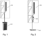
- baseband unit In a traditional macro configuration, baseband unit is physically bound to radio unit. In real deployment, both of the baseband unit and the radio unit are put together in a cabinet (102) as shown in Figure 1 on the ground, while antenna unit (101) is always horizontally higher than the radio unit, usually located at the top of buildings in the city or on the mountains in countryside, to ensure the transmission and reception of electromagnetic waves. Long jumper cable is used to connect the radio unit and the antenna unit (101) in Figure 1 .
- Radio unit (202) is not necessarily close to baseband unit (203) but installed considerably close to antenna unit (201) , shown in Figure 2 . However, connection between antenna unit (201) and radio unit (202) still relies on jumper cable.
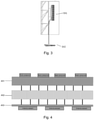
- antenna integrated radio unit was designed to put radio unit and antenna unit into one physical "box” (301) as shown in Figure 3 .
- Long cable is needed between the physical box (301) and baseband unit (302) .
- MIMO Multiple In and Multiple Out
- number of antenna element has been increased from one or two to eight or even 16.
- antenna technology development turned it into reality that antenna element can be made into planar antenna element and be patched onto an antenna layer.
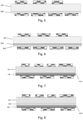
- Radio Unit (401) includes a multi-layer Printed Circuit Board (PCB) with several radio components mounted on one side of the radio PCB.
- Antenna Unit (403) includes an antenna PCB and several antenna elements patched on one side of the antenna PCB.
- a Filter Unit (402) is between the radio PCB and antenna PCB to filter out unnecessary interference outside required spectrum. Each side of the filter unit is connected to the other side of the radio PCB and the antenna PCB respectively. Signals transmitted between the radio unit and antenna unit go through the wired connection.
- a plurality of antenna elements are designed to transmit signals through a plurality of radio branches.
- N radio branches are designed, there are N connectors between a filter unit and an antenna unit, and N connectors between the filter unit and a radio unit.
- the cost of the connectors is rather high, but the difficulty of assembling the 2N connectors is considerable especially N increases to 64 which is popular in the 4th generation (4G) telecommunication system.
- US 2015/381229 A1 suggests an antenna system comprising an antenna printed circuit board (PCB) placed externally on a multilayer PCB.
- PCB printed circuit board
- EP 3361566 A1 suggests a base station in that modules of the base station are integrated together and consequently a capacity of single kind of modules cannot be expanded independently.
- EP 2755276A1 suggests an antenna apparatus is provided, including: an antenna component that is arranged on a passive side of the antenna apparatus; a radio frequency unit that is arranged on an active side of the antenna apparatus.
- US 2011/159824 A1 suggests an active antenna array for a mobile communications network.
- the active antenna array comprises a plurality of antenna elements, at least one first conductive sheet and at least one second conductive sheet.
- the plurality of antenna elements terminates at least one relay path.
- the present disclosure proposes to integrate an antenna part and a radio part into one printed circuit board assembled in a communication node, so as to leave out legacy connectors from the filter unit respectively to the antenna unit and the radio unit.
- a wireless communication node in a wireless communication node, legacy connectors between a filter unit and an antenna unit, and connectors between the filter unit and a radio unit are left out, while an antenna part and a radio part are integrated into a single PCB.
- the PCB can be reduced in size and increase in reliability.
- the cost of the connectors can be saved and the assembling of the communication node can be simplified. What's more, the communication node can be designed in a more efficient manner.
- the present disclosure proposes to integrate an antenna part and a radio part into a single integral printed circuit board (PCB) which is to be assembled in a wireless communication node. What's more, the present disclosure provides a wireless communication node in which the integral PCB is assembled.
- PCB printed circuit board
- FIG. 5 shows a cross sectional view illustrating one of our proposed embodiments.
- An embodiment provides a multi-layer Printed Circuit Board in a wireless communication node.
- the PCB comprises:
- the above mentioned multi-layer PCB further comprise an isolator layer (603) between the multiple radio layers and the at least one antenna layer.
- the isolator layer is mainly to shield the multiple radio layers from radiation of the at least one antenna element, so that signal processing and transmitting by the at least one radio component and the multiple radio layers would not be interfered by the electromagnetic radiation of the antenna element (s) .
- the isolator layer (603) is mainly made of copper or gold-copper alloy.
- the isolator layer includes a substrate coated with copper or some metal alloy.
- the thickness of the isolator layer is preferably similar to average thickness of a layer in the multi-layer PCB, such as between 0.2 ⁇ 0.3 mm. However, this is not the present disclosure mainly focusing on.
- the above mentioned multi-layer PCB further comprises ground planes respectively included in the multiple radio layers (701) and the at least one antenna layer (702) .
- Ground plan in the multiple radio layers may be designed to keep away from antenna radiation without an isolator layer between the multiple radio layers and the at least one antenna layer.
- Ground plane in the at least one antenna layer is designed to decrease radiation influence upon the at least one radio component. More specifically, the at least one antenna layer comprise an entire layer (7021) of the ground plane which is next to the multiple radio layers (701) .
- the thickness of the ground plane layer of the at least one antenna layer is preferably between 0.5 ⁇ 0.8 mm, compared to 0.2 ⁇ 0.3 mm thickness of the isolator layer as proposed above.
- ground planes respectively included in the multiple radio layers and the at least one antenna layer may remain their conventional designs such as metal area and thickness, to some extent lower down the complexity of the PCB design.
- the filter unit In a current AIR design, the filter unit is usually designed as a cavity filter which is known for low insertion loss and higher power handling ability. On the other hand, it is an unavoidable barrier to decrease the size of the AIR because of size limitation of cavity filter.
- new frequency band is introduced as ultra-high frequency and super-high frequency, such as radio frequency above 2 ⁇ 3GHz as ultra-high frequency and above 3G as super-high frequency.
- filter technology can be mounted upon a surface of a PCB especially in high (above 3MHz) frequency circumstances. Super-high and ultra-high frequency circumstances are now looking forward to a widespread use of the surface mounted filters.
- Monoblock filter is an example of the surface mounted filters.
- Dielectric filter is one of the preferable types.
- alternatives such as Multilayer filter, Bulk Acoustic Waves (BAW) Filter, or Surface Acoustic Waves (SAW) Filter.
- SAW Finite Impulse Response (FIR) filter or low loss filter, BAW filter on Quartz or on Lithium Tantalate (LT) are options of SAW and BAW filters, respectively.
- radio components include:
- Transceiver transmits and receives signals to and from the baseband part.
- Power Amplifier is to amplify signals from TRX for transmission through antenna element(s).
- the at least one radio component to be mounted on the surface of the radio layer comprises one or more baseband components which belong to the baseband part, as shown either Figure 7 or Figure 8 .
- the baseband components comprise: Field Programmable Gate Array (FPGA) , Digital Signal Processor (DSP) , Central Process Unit (CPU) and Random Access Memory (RAM) .
- the one or more baseband components play a role of baseband signal processing such as modulation/demodulation, encoding/decoding, pre-coding, channel estimation and equalization, which means that baseband functions are also integrated into a same multi-layer PCB with the radio function.
- the connection between the transceiver and the baseband components no longer relies on external optical fiber but wirings embedded in the PCB. In that way, hidden trouble to the reliability raised by external cable can be impeded, especially poor contact in the connector at the ends of the external cable. Meanwhile, cost of the long external cable can be saved.
- An access node provided by the embodiments in the present disclosure can be smaller in size since the antenna part and the radio part are integrated into a same PCB, rooms for conventional connectors and jumper cables between the connectors can be saved, Moreover, weight of the access node will also be decreased with the removal of the conventional connectors and cables. Therefore, it will be easier to install a lighter and smaller access node as presented on the spot.
- assembling difficulty is a big concern when connectors are assembled, especially a large number of pins plugging into holes densely arranged. It is frequently happened that some of the pins are misplaced when spacing of pins and spacing of holes are not exactly matching. With this invention, assembling of those connectors can be avoided.
- cost of the access node can also be saved.
- An access node supporting N radio branches' transmission may need 2*N connectors because connector need to be applied for radio unit to filter unit connection, and filter unit to antenna unit connection. Assuming N is 128 which will be popularly supported in 5G, 256 connectors are needed for one access node. With an average price around US$3 of a connector, material expense of US$768 will be saved for a single access node, not to say the scrap of an entire N-head connector when some of the pins are misplaced during assembling.
- connection reliability is also a problem of the conventional access node in a long-term concern. Insertion part of the pins is apt to be oxidized which might affect the conductivity. Influence on the connector from external environment such as severe weather might accelerate burn-in of the entire access node during its product lifetime. With the radio part and the antenna part integrated in a single PCB, reliability of the connection is enhanced.
- a wireless communication node into which the multi-layer PCB is assembled is not limited to an access node.
- a wireless communication node can be a wireless terminal device of which a user equipment is a representative example.
- a user equipment usually comprises two to four antenna elements at most, while in future development such as 5G deployment, number of antenna elements in a user equipment is anticipated to be 8, 16 or even more. Therefore, design of a surface antenna layer patched with multiple antenna elements is sound to minimize size of the user equipment with multiple antennas. What's more, besides the benefit discussed above, since connectors are saved in the PCB, yield rate of user equipment can be improved.
- the at least one radio component includes a surface mounted filter, such that the size of the terminal device can be considerably decreased. In that case, a user equipment such as mobile phone or mobile tablet can be thinner thus more popular as a portable device, catering to the needs of the users. Furthermore, the at least one radio component includes a TRX component. In the circumstance that does not form part of the invention that a Power Amplify (PA) is not mounted on the PCB, the TRX component not only transmits and receives RF signals through air interface, but amplifies RF signals before transmission. Further, baseband components are also mounted on the surface radio layer in the user equipment.
- PA Power Amplify
- an isolation layer is in-between the multiple radio layers and the at least one antenna layer, to shield the multiple radio layers from radiation of the at least one antenna element.
- the isolation layer can be further connected to a shell of the user equipment.
- Respective ground plane of the multiple radio layers and the at least one antenna layer are also connected to the shell of the user equipment.
- ground planes of the multiple radio layers and the at least one antenna layer can be designed to minimize the affection of radiation to the radio components, such that an isolation layer is not necessary in the middle of the multi-layer PCB.
Landscapes
- Engineering & Computer Science (AREA)
- Microelectronics & Electronic Packaging (AREA)
- Computer Networks & Wireless Communication (AREA)
- Physics & Mathematics (AREA)
- Electromagnetism (AREA)
- Signal Processing (AREA)
- Manufacturing & Machinery (AREA)
- Transceivers (AREA)
- Condensed Matter Physics & Semiconductors (AREA)
- General Physics & Mathematics (AREA)
- Computer Hardware Design (AREA)
- Power Engineering (AREA)
Claims (9)
- Mehrschichtige Leiterplatte, PCB, für einen drahtlosen Kommunikationsknoten, umfassend:mehrere Funkschichten (501, 601) auf einer Seite der mehrschichtigen PCB, wobei mindestens eine Funkkomponente auf einer Oberflächenschicht der mehreren Funkschichten montiert werden soll, wobei die mindestens eine Funkkomponente einen oberflächenmontierten Filter, Leistungsverstärker (PA) und Transceiver (TRX)-Komponente umfasst; undmindestens eine Antennenschicht (502, 602) auf einer anderen Seite der mehrschichtigen PCB, wobei ein Antennenelement auf einer Oberflächenschicht der mindestens einen Antennenschicht eingesetzt ist.
- Mehrschichtige PCB nach Anspruch 1, ferner umfassend:
eine Isolatorschicht (603) zwischen den mehreren Funkschichten und der mindestens einen Antennenschicht. - Mehrschichtige PCB nach Anspruch 1 oder 2, wobei die mehreren Funkschichten eine Masseebene umfassen und die mindestens eine Antennenschicht eine Masseebenenschicht (7021, 8031) umfasst.
- Mehrschichtige PCB nach einem der Ansprüche 1 bis 3, wobei die mindestens eine Funkkomponente eine oder mehrere Basisbandkomponenten umfasst von: FPGA, DSP, CPU und RAM.
- Mehrschichtige PCB nach einem der Ansprüche 1 bis 4, wobei der drahtlose Kommunikationsknoten ein Endgerät oder ein Zugangsknoten ist.
- Drahtloser Kommunikationsknoten für ein drahtloses Telekommunikationssystem,
wobei der drahtlose Kommunikationsknoten Folgendes umfasst:
eine mehrschichtige PCB nach einem der Ansprüche 1 bis 5. - Drahtloser Kommunikationsknoten nach Anspruch 6, wobei das mindestens eine Antennenelement eines oder mehrere von Folgendem umfasst: Hochfrequenz-Antennenelement, Superhochfrequenz-Antennenelement oder Ultrahochfrequenz-Antennenelement.
- Drahtloser Kommunikationsknoten nach einem der Ansprüche 6 bis 7, wobei der drahtlose Kommunikationsknoten in einem Multi-Eingang-Multi-Ausgang, MIMO,-System ist.
- Drahtloser Kommunikationsknoten nach einem der Ansprüche 6 bis 8, wobei der drahtlose Kommunikationsknoten ein Zugangsknoten oder ein Endgerät ist.
Priority Applications (2)
| Application Number | Priority Date | Filing Date | Title |
|---|---|---|---|
| PL16903436T PL3465752T3 (pl) | 2016-05-31 | 2016-05-31 | Wielowarstwowa płytka obwodu drukowanego i węzeł komunikacji bezprzewodowej |
| EP21211777.4A EP4050651A1 (de) | 2016-05-31 | 2016-05-31 | Mehrschichtige leiterplatte und drahtloskommunikationsknoten |
Applications Claiming Priority (1)
| Application Number | Priority Date | Filing Date | Title |
|---|---|---|---|
| PCT/CN2016/084026 WO2017206049A1 (en) | 2016-05-31 | 2016-05-31 | A multi-layer printed circuit board and a wireless communication node |
Related Child Applications (2)
| Application Number | Title | Priority Date | Filing Date |
|---|---|---|---|
| EP21211777.4A Division-Into EP4050651A1 (de) | 2016-05-31 | 2016-05-31 | Mehrschichtige leiterplatte und drahtloskommunikationsknoten |
| EP21211777.4A Division EP4050651A1 (de) | 2016-05-31 | 2016-05-31 | Mehrschichtige leiterplatte und drahtloskommunikationsknoten |
Publications (3)
| Publication Number | Publication Date |
|---|---|
| EP3465752A1 EP3465752A1 (de) | 2019-04-10 |
| EP3465752A4 EP3465752A4 (de) | 2020-01-01 |
| EP3465752B1 true EP3465752B1 (de) | 2022-03-02 |
Family
ID=60479435
Family Applications (2)
| Application Number | Title | Priority Date | Filing Date |
|---|---|---|---|
| EP16903436.0A Active EP3465752B1 (de) | 2016-05-31 | 2016-05-31 | Mehrschichtige leiterplatte und drahtloskommunikationsknoten |
| EP21211777.4A Pending EP4050651A1 (de) | 2016-05-31 | 2016-05-31 | Mehrschichtige leiterplatte und drahtloskommunikationsknoten |
Family Applications After (1)
| Application Number | Title | Priority Date | Filing Date |
|---|---|---|---|
| EP21211777.4A Pending EP4050651A1 (de) | 2016-05-31 | 2016-05-31 | Mehrschichtige leiterplatte und drahtloskommunikationsknoten |
Country Status (5)
| Country | Link |
|---|---|
| US (1) | US10201073B2 (de) |
| EP (2) | EP3465752B1 (de) |
| CN (2) | CN109219882A (de) |
| PL (1) | PL3465752T3 (de) |
| WO (1) | WO2017206049A1 (de) |
Families Citing this family (6)
| Publication number | Priority date | Publication date | Assignee | Title |
|---|---|---|---|---|
| CN108281787B (zh) * | 2018-01-17 | 2021-04-16 | Oppo广东移动通信有限公司 | 电子装置 |
| CN110323565A (zh) * | 2019-04-30 | 2019-10-11 | 深圳市大富科技股份有限公司 | 一种基站天线以及用于基站的有源天线单元 |
| KR102738877B1 (ko) | 2020-06-05 | 2024-12-06 | 삼성전자주식회사 | 무선 통신 시스템에서 안테나 필터 및 이를 포함하는 전자 장치 |
| EP4222814A4 (de) * | 2020-09-29 | 2024-06-05 | Telefonaktiebolaget LM Ericsson (publ) | Basisstation |
| EP4275461A1 (de) * | 2021-01-08 | 2023-11-15 | Telefonaktiebolaget LM Ericsson (publ) | Funkkühlkörper, funkeinheit und basisstation |
| TWI884417B (zh) | 2023-02-15 | 2025-05-21 | 繁晶科技股份有限公司 | 用於多天線射頻單元、基地台、以及衛星通訊之電路架構 |
Family Cites Families (16)
| Publication number | Priority date | Publication date | Assignee | Title |
|---|---|---|---|---|
| EP1562258A4 (de) * | 2002-11-15 | 2006-05-24 | Panasonic Mobile Comm Co Ltd | Aktive antenne |
| CN1630133A (zh) * | 2003-12-18 | 2005-06-22 | 摩托罗拉公司 | 天线辐射器装置和无线通信装置 |
| US8035565B2 (en) * | 2006-03-17 | 2011-10-11 | Nxp B.V. | Antenna device and RF communication equipment |
| US20090153423A1 (en) * | 2007-12-13 | 2009-06-18 | Motorola, Inc. | Wireless communication device with a multi-band antenna system |
| US20090180260A1 (en) * | 2008-01-10 | 2009-07-16 | Qimonda Ag | Memory module, method for manufacturing a memory module and computer system |
| CN101728369B (zh) | 2008-10-28 | 2014-05-07 | 赛伊公司 | 表面可安装的集成电路封装方法 |
| US20110159824A1 (en) | 2009-12-31 | 2011-06-30 | Peter Kenington | Active antenna array for a mobile communications network employing a first conductive layer and a second conductive layer |
| WO2012092521A1 (en) * | 2010-12-29 | 2012-07-05 | Secureall Corporation | True omni-directional antenna |
| KR101806942B1 (ko) * | 2011-09-28 | 2017-12-08 | 삼성전자주식회사 | 휴대단말기의 근거리무선통신 안테나장치 |
| CN102509852A (zh) | 2011-09-28 | 2012-06-20 | 华为技术有限公司 | 天线装置 |
| US8648454B2 (en) * | 2012-02-14 | 2014-02-11 | International Business Machines Corporation | Wafer-scale package structures with integrated antennas |
| US9391370B2 (en) * | 2014-06-30 | 2016-07-12 | Samsung Electronics Co., Ltd. | Antenna feed integrated on multi-layer PCB |
| US9936571B2 (en) * | 2015-09-02 | 2018-04-03 | Sae Magnetics (H.K.) Ltd. | Printed circuit board |
| CN106571518A (zh) | 2015-10-09 | 2017-04-19 | 中兴通讯股份有限公司 | 基站 |
| CN105552550B (zh) * | 2016-01-30 | 2019-08-20 | 华为技术有限公司 | 一种贴片天线单元及天线 |
| US10103424B2 (en) * | 2016-04-26 | 2018-10-16 | Apple Inc. | Electronic device with millimeter wave yagi antennas |
-
2016
- 2016-05-31 EP EP16903436.0A patent/EP3465752B1/de active Active
- 2016-05-31 WO PCT/CN2016/084026 patent/WO2017206049A1/en not_active Ceased
- 2016-05-31 EP EP21211777.4A patent/EP4050651A1/de active Pending
- 2016-05-31 US US15/515,242 patent/US10201073B2/en active Active
- 2016-05-31 CN CN201680086254.7A patent/CN109219882A/zh active Pending
- 2016-05-31 PL PL16903436T patent/PL3465752T3/pl unknown
- 2016-05-31 CN CN202311632574.6A patent/CN117613545A/zh active Pending
Also Published As
| Publication number | Publication date |
|---|---|
| US10201073B2 (en) | 2019-02-05 |
| CN109219882A (zh) | 2019-01-15 |
| CN117613545A (zh) | 2024-02-27 |
| US20180192508A1 (en) | 2018-07-05 |
| EP3465752A4 (de) | 2020-01-01 |
| EP3465752A1 (de) | 2019-04-10 |
| PL3465752T3 (pl) | 2022-06-13 |
| WO2017206049A1 (en) | 2017-12-07 |
| EP4050651A1 (de) | 2022-08-31 |
Similar Documents
| Publication | Publication Date | Title |
|---|---|---|
| EP3465752B1 (de) | Mehrschichtige leiterplatte und drahtloskommunikationsknoten | |
| US10270152B2 (en) | Broadband transceiver and distributed antenna system utilizing same | |
| KR102887421B1 (ko) | 무선 통신 시스템에서 안테나 필터 및 이를 포함하는 전자 장치 | |
| WO2020247606A1 (en) | Radio frequency signal boosters serving as outdoor infrastructure in high frequency cellular networks | |
| JP7162062B2 (ja) | 通信デバイスおよび通信デバイスにおける方法 | |
| CN114830434B (zh) | 一种封装天线装置和无线通信装置 | |
| US12470259B2 (en) | Antenna filter and electronic device including same in wireless communication system | |
| US12519245B2 (en) | Antenna module with flexible arrangement and manufacturing method thereof | |
| CN101340014A (zh) | 带凹槽的陶瓷电介质滤波器和双工器 | |
| KR102738877B1 (ko) | 무선 통신 시스템에서 안테나 필터 및 이를 포함하는 전자 장치 | |
| US9627750B2 (en) | Radio device | |
| US9893434B2 (en) | Multi-element omni-directional antenna | |
| KR20230141737A (ko) | 매시브 mimo 무선 유닛의 afu(antenna filter unit)의 시스템 및 설계 방법 | |
| US11979218B1 (en) | Radio frequency signal boosters serving as outdoor infrastructure in high frequency cellular networks | |
| HK40078685A (en) | A multi-layer printed circuit board and a wireless communication node | |
| KR102919910B1 (ko) | 무선 통신 시스템에서 안테나 필터 및 이를 포함하는 전자 장치 | |
| EP4053993A1 (de) | Wellenleiterkreuzkopplungsfilter mit mehreren parallelen hohlräumen | |
| CN120674815A (zh) | 一种频率选择装置、基站天线和基站设备 | |
| US20240421500A1 (en) | Antenna assembly and manufacturing method thereof, array antenna and manufacturing method thereof, and communication device | |
| CN214069924U (zh) | 一种通信设备 | |
| KR20230141735A (ko) | 대규모 mimo 라디오 유닛의 rf 프론트 엔드 모듈의 시스템 및 설계 방법 | |
| JP2006033626A (ja) | アンテナシステム |
Legal Events
| Date | Code | Title | Description |
|---|---|---|---|
| STAA | Information on the status of an ep patent application or granted ep patent |
Free format text: STATUS: THE INTERNATIONAL PUBLICATION HAS BEEN MADE |
|
| PUAI | Public reference made under article 153(3) epc to a published international application that has entered the european phase |
Free format text: ORIGINAL CODE: 0009012 |
|
| STAA | Information on the status of an ep patent application or granted ep patent |
Free format text: STATUS: REQUEST FOR EXAMINATION WAS MADE |
|
| 17P | Request for examination filed |
Effective date: 20181127 |
|
| AK | Designated contracting states |
Kind code of ref document: A1 Designated state(s): AL AT BE BG CH CY CZ DE DK EE ES FI FR GB GR HR HU IE IS IT LI LT LU LV MC MK MT NL NO PL PT RO RS SE SI SK SM TR |
|
| AX | Request for extension of the european patent |
Extension state: BA ME |
|
| DAV | Request for validation of the european patent (deleted) | ||
| DAX | Request for extension of the european patent (deleted) | ||
| A4 | Supplementary search report drawn up and despatched |
Effective date: 20191202 |
|
| RIC1 | Information provided on ipc code assigned before grant |
Ipc: H01L 23/00 20060101ALI20191126BHEP Ipc: H05K 1/02 20060101ALI20191126BHEP Ipc: H01L 25/00 20060101AFI20191126BHEP Ipc: H01Q 21/00 20060101ALI20191126BHEP Ipc: H05K 1/16 20060101ALI20191126BHEP Ipc: H01Q 9/04 20060101ALN20191126BHEP Ipc: H01Q 1/38 20060101ALI20191126BHEP Ipc: H01Q 1/24 20060101ALI20191126BHEP |
|
| GRAP | Despatch of communication of intention to grant a patent |
Free format text: ORIGINAL CODE: EPIDOSNIGR1 |
|
| STAA | Information on the status of an ep patent application or granted ep patent |
Free format text: STATUS: GRANT OF PATENT IS INTENDED |
|
| RIC1 | Information provided on ipc code assigned before grant |
Ipc: H01Q 9/04 20060101ALN20210604BHEP Ipc: H01Q 1/24 20060101ALI20210604BHEP Ipc: H05K 1/16 20060101ALI20210604BHEP Ipc: H05K 1/02 20060101ALI20210604BHEP Ipc: H01Q 21/00 20060101ALI20210604BHEP Ipc: H01Q 1/38 20060101ALI20210604BHEP Ipc: H01L 23/00 20060101ALI20210604BHEP Ipc: H01L 25/00 20060101AFI20210604BHEP |
|
| INTG | Intention to grant announced |
Effective date: 20210629 |
|
| GRAJ | Information related to disapproval of communication of intention to grant by the applicant or resumption of examination proceedings by the epo deleted |
Free format text: ORIGINAL CODE: EPIDOSDIGR1 |
|
| STAA | Information on the status of an ep patent application or granted ep patent |
Free format text: STATUS: REQUEST FOR EXAMINATION WAS MADE |
|
| INTC | Intention to grant announced (deleted) | ||
| GRAP | Despatch of communication of intention to grant a patent |
Free format text: ORIGINAL CODE: EPIDOSNIGR1 |
|
| STAA | Information on the status of an ep patent application or granted ep patent |
Free format text: STATUS: GRANT OF PATENT IS INTENDED |
|
| RIC1 | Information provided on ipc code assigned before grant |
Ipc: H01Q 9/04 20060101ALN20211020BHEP Ipc: H01Q 1/24 20060101ALI20211020BHEP Ipc: H05K 1/16 20060101ALI20211020BHEP Ipc: H05K 1/02 20060101ALI20211020BHEP Ipc: H01Q 21/00 20060101ALI20211020BHEP Ipc: H01Q 1/38 20060101ALI20211020BHEP Ipc: H01L 23/00 20060101ALI20211020BHEP Ipc: H01L 25/00 20060101AFI20211020BHEP |
|
| INTG | Intention to grant announced |
Effective date: 20211117 |
|
| GRAS | Grant fee paid |
Free format text: ORIGINAL CODE: EPIDOSNIGR3 |
|
| GRAA | (expected) grant |
Free format text: ORIGINAL CODE: 0009210 |
|
| STAA | Information on the status of an ep patent application or granted ep patent |
Free format text: STATUS: THE PATENT HAS BEEN GRANTED |
|
| AK | Designated contracting states |
Kind code of ref document: B1 Designated state(s): AL AT BE BG CH CY CZ DE DK EE ES FI FR GB GR HR HU IE IS IT LI LT LU LV MC MK MT NL NO PL PT RO RS SE SI SK SM TR |
|
| REG | Reference to a national code |
Ref country code: GB Ref legal event code: FG4D |
|
| REG | Reference to a national code |
Ref country code: CH Ref legal event code: EP Ref country code: AT Ref legal event code: REF Ref document number: 1472942 Country of ref document: AT Kind code of ref document: T Effective date: 20220315 |
|
| REG | Reference to a national code |
Ref country code: DE Ref legal event code: R096 Ref document number: 602016069730 Country of ref document: DE |
|
| REG | Reference to a national code |
Ref country code: IE Ref legal event code: FG4D |
|
| REG | Reference to a national code |
Ref country code: LT Ref legal event code: MG9D |
|
| REG | Reference to a national code |
Ref country code: NL Ref legal event code: MP Effective date: 20220302 |
|
| PG25 | Lapsed in a contracting state [announced via postgrant information from national office to epo] |
Ref country code: SE Free format text: LAPSE BECAUSE OF FAILURE TO SUBMIT A TRANSLATION OF THE DESCRIPTION OR TO PAY THE FEE WITHIN THE PRESCRIBED TIME-LIMIT Effective date: 20220302 Ref country code: RS Free format text: LAPSE BECAUSE OF FAILURE TO SUBMIT A TRANSLATION OF THE DESCRIPTION OR TO PAY THE FEE WITHIN THE PRESCRIBED TIME-LIMIT Effective date: 20220302 Ref country code: NO Free format text: LAPSE BECAUSE OF FAILURE TO SUBMIT A TRANSLATION OF THE DESCRIPTION OR TO PAY THE FEE WITHIN THE PRESCRIBED TIME-LIMIT Effective date: 20220602 Ref country code: LT Free format text: LAPSE BECAUSE OF FAILURE TO SUBMIT A TRANSLATION OF THE DESCRIPTION OR TO PAY THE FEE WITHIN THE PRESCRIBED TIME-LIMIT Effective date: 20220302 Ref country code: HR Free format text: LAPSE BECAUSE OF FAILURE TO SUBMIT A TRANSLATION OF THE DESCRIPTION OR TO PAY THE FEE WITHIN THE PRESCRIBED TIME-LIMIT Effective date: 20220302 Ref country code: ES Free format text: LAPSE BECAUSE OF FAILURE TO SUBMIT A TRANSLATION OF THE DESCRIPTION OR TO PAY THE FEE WITHIN THE PRESCRIBED TIME-LIMIT Effective date: 20220302 Ref country code: BG Free format text: LAPSE BECAUSE OF FAILURE TO SUBMIT A TRANSLATION OF THE DESCRIPTION OR TO PAY THE FEE WITHIN THE PRESCRIBED TIME-LIMIT Effective date: 20220602 |
|
| REG | Reference to a national code |
Ref country code: AT Ref legal event code: MK05 Ref document number: 1472942 Country of ref document: AT Kind code of ref document: T Effective date: 20220302 |
|
| PG25 | Lapsed in a contracting state [announced via postgrant information from national office to epo] |
Ref country code: LV Free format text: LAPSE BECAUSE OF FAILURE TO SUBMIT A TRANSLATION OF THE DESCRIPTION OR TO PAY THE FEE WITHIN THE PRESCRIBED TIME-LIMIT Effective date: 20220302 Ref country code: GR Free format text: LAPSE BECAUSE OF FAILURE TO SUBMIT A TRANSLATION OF THE DESCRIPTION OR TO PAY THE FEE WITHIN THE PRESCRIBED TIME-LIMIT Effective date: 20220603 Ref country code: FI Free format text: LAPSE BECAUSE OF FAILURE TO SUBMIT A TRANSLATION OF THE DESCRIPTION OR TO PAY THE FEE WITHIN THE PRESCRIBED TIME-LIMIT Effective date: 20220302 |
|
| PG25 | Lapsed in a contracting state [announced via postgrant information from national office to epo] |
Ref country code: NL Free format text: LAPSE BECAUSE OF FAILURE TO SUBMIT A TRANSLATION OF THE DESCRIPTION OR TO PAY THE FEE WITHIN THE PRESCRIBED TIME-LIMIT Effective date: 20220302 |
|
| PG25 | Lapsed in a contracting state [announced via postgrant information from national office to epo] |
Ref country code: SM Free format text: LAPSE BECAUSE OF FAILURE TO SUBMIT A TRANSLATION OF THE DESCRIPTION OR TO PAY THE FEE WITHIN THE PRESCRIBED TIME-LIMIT Effective date: 20220302 Ref country code: SK Free format text: LAPSE BECAUSE OF FAILURE TO SUBMIT A TRANSLATION OF THE DESCRIPTION OR TO PAY THE FEE WITHIN THE PRESCRIBED TIME-LIMIT Effective date: 20220302 Ref country code: RO Free format text: LAPSE BECAUSE OF FAILURE TO SUBMIT A TRANSLATION OF THE DESCRIPTION OR TO PAY THE FEE WITHIN THE PRESCRIBED TIME-LIMIT Effective date: 20220302 Ref country code: PT Free format text: LAPSE BECAUSE OF FAILURE TO SUBMIT A TRANSLATION OF THE DESCRIPTION OR TO PAY THE FEE WITHIN THE PRESCRIBED TIME-LIMIT Effective date: 20220704 Ref country code: EE Free format text: LAPSE BECAUSE OF FAILURE TO SUBMIT A TRANSLATION OF THE DESCRIPTION OR TO PAY THE FEE WITHIN THE PRESCRIBED TIME-LIMIT Effective date: 20220302 Ref country code: CZ Free format text: LAPSE BECAUSE OF FAILURE TO SUBMIT A TRANSLATION OF THE DESCRIPTION OR TO PAY THE FEE WITHIN THE PRESCRIBED TIME-LIMIT Effective date: 20220302 Ref country code: AT Free format text: LAPSE BECAUSE OF FAILURE TO SUBMIT A TRANSLATION OF THE DESCRIPTION OR TO PAY THE FEE WITHIN THE PRESCRIBED TIME-LIMIT Effective date: 20220302 |
|
| PG25 | Lapsed in a contracting state [announced via postgrant information from national office to epo] |
Ref country code: IS Free format text: LAPSE BECAUSE OF FAILURE TO SUBMIT A TRANSLATION OF THE DESCRIPTION OR TO PAY THE FEE WITHIN THE PRESCRIBED TIME-LIMIT Effective date: 20220702 Ref country code: AL Free format text: LAPSE BECAUSE OF FAILURE TO SUBMIT A TRANSLATION OF THE DESCRIPTION OR TO PAY THE FEE WITHIN THE PRESCRIBED TIME-LIMIT Effective date: 20220302 |
|
| REG | Reference to a national code |
Ref country code: DE Ref legal event code: R097 Ref document number: 602016069730 Country of ref document: DE |
|
| REG | Reference to a national code |
Ref country code: CH Ref legal event code: PL |
|
| PLBE | No opposition filed within time limit |
Free format text: ORIGINAL CODE: 0009261 |
|
| STAA | Information on the status of an ep patent application or granted ep patent |
Free format text: STATUS: NO OPPOSITION FILED WITHIN TIME LIMIT |
|
| REG | Reference to a national code |
Ref country code: BE Ref legal event code: MM Effective date: 20220531 |
|
| PG25 | Lapsed in a contracting state [announced via postgrant information from national office to epo] |
Ref country code: MC Free format text: LAPSE BECAUSE OF FAILURE TO SUBMIT A TRANSLATION OF THE DESCRIPTION OR TO PAY THE FEE WITHIN THE PRESCRIBED TIME-LIMIT Effective date: 20220302 Ref country code: LU Free format text: LAPSE BECAUSE OF NON-PAYMENT OF DUE FEES Effective date: 20220531 Ref country code: LI Free format text: LAPSE BECAUSE OF NON-PAYMENT OF DUE FEES Effective date: 20220531 Ref country code: DK Free format text: LAPSE BECAUSE OF FAILURE TO SUBMIT A TRANSLATION OF THE DESCRIPTION OR TO PAY THE FEE WITHIN THE PRESCRIBED TIME-LIMIT Effective date: 20220302 Ref country code: CH Free format text: LAPSE BECAUSE OF NON-PAYMENT OF DUE FEES Effective date: 20220531 |
|
| 26N | No opposition filed |
Effective date: 20221205 |
|
| PG25 | Lapsed in a contracting state [announced via postgrant information from national office to epo] |
Ref country code: SI Free format text: LAPSE BECAUSE OF FAILURE TO SUBMIT A TRANSLATION OF THE DESCRIPTION OR TO PAY THE FEE WITHIN THE PRESCRIBED TIME-LIMIT Effective date: 20220302 |
|
| PG25 | Lapsed in a contracting state [announced via postgrant information from national office to epo] |
Ref country code: IE Free format text: LAPSE BECAUSE OF NON-PAYMENT OF DUE FEES Effective date: 20220531 Ref country code: FR Free format text: LAPSE BECAUSE OF NON-PAYMENT OF DUE FEES Effective date: 20220531 |
|
| PG25 | Lapsed in a contracting state [announced via postgrant information from national office to epo] |
Ref country code: BE Free format text: LAPSE BECAUSE OF NON-PAYMENT OF DUE FEES Effective date: 20220531 |
|
| P01 | Opt-out of the competence of the unified patent court (upc) registered |
Effective date: 20230523 |
|
| PG25 | Lapsed in a contracting state [announced via postgrant information from national office to epo] |
Ref country code: IT Free format text: LAPSE BECAUSE OF FAILURE TO SUBMIT A TRANSLATION OF THE DESCRIPTION OR TO PAY THE FEE WITHIN THE PRESCRIBED TIME-LIMIT Effective date: 20220302 |
|
| PG25 | Lapsed in a contracting state [announced via postgrant information from national office to epo] |
Ref country code: HU Free format text: LAPSE BECAUSE OF FAILURE TO SUBMIT A TRANSLATION OF THE DESCRIPTION OR TO PAY THE FEE WITHIN THE PRESCRIBED TIME-LIMIT; INVALID AB INITIO Effective date: 20160531 |
|
| PG25 | Lapsed in a contracting state [announced via postgrant information from national office to epo] |
Ref country code: MK Free format text: LAPSE BECAUSE OF FAILURE TO SUBMIT A TRANSLATION OF THE DESCRIPTION OR TO PAY THE FEE WITHIN THE PRESCRIBED TIME-LIMIT Effective date: 20220302 Ref country code: CY Free format text: LAPSE BECAUSE OF FAILURE TO SUBMIT A TRANSLATION OF THE DESCRIPTION OR TO PAY THE FEE WITHIN THE PRESCRIBED TIME-LIMIT Effective date: 20220302 |
|
| PG25 | Lapsed in a contracting state [announced via postgrant information from national office to epo] |
Ref country code: MT Free format text: LAPSE BECAUSE OF FAILURE TO SUBMIT A TRANSLATION OF THE DESCRIPTION OR TO PAY THE FEE WITHIN THE PRESCRIBED TIME-LIMIT Effective date: 20220302 |
|
| PGFP | Annual fee paid to national office [announced via postgrant information from national office to epo] |
Ref country code: DE Payment date: 20250529 Year of fee payment: 10 Ref country code: PL Payment date: 20250508 Year of fee payment: 10 |
|
| PGFP | Annual fee paid to national office [announced via postgrant information from national office to epo] |
Ref country code: GB Payment date: 20250527 Year of fee payment: 10 |
|
| PGFP | Annual fee paid to national office [announced via postgrant information from national office to epo] |
Ref country code: TR Payment date: 20250515 Year of fee payment: 10 |
|
| REG | Reference to a national code |
Ref country code: DE Ref legal event code: R079 Ref document number: 602016069730 Country of ref document: DE Free format text: PREVIOUS MAIN CLASS: H01L0025000000 Ipc: H10W0090000000 |