EP3462543B1 - Array antenna - Google Patents
Array antenna Download PDFInfo
- Publication number
- EP3462543B1 EP3462543B1 EP18179805.9A EP18179805A EP3462543B1 EP 3462543 B1 EP3462543 B1 EP 3462543B1 EP 18179805 A EP18179805 A EP 18179805A EP 3462543 B1 EP3462543 B1 EP 3462543B1
- Authority
- EP
- European Patent Office
- Prior art keywords
- array antenna
- feeding
- metal layer
- antenna according
- metal
- Prior art date
- Legal status (The legal status is an assumption and is not a legal conclusion. Google has not performed a legal analysis and makes no representation as to the accuracy of the status listed.)
- Active
Links
- 239000002184 metal Substances 0.000 claims description 58
- 229910052751 metal Inorganic materials 0.000 claims description 58
- 239000000758 substrate Substances 0.000 claims description 29
- 230000005540 biological transmission Effects 0.000 claims description 23
- 230000008878 coupling Effects 0.000 claims description 21
- 238000010168 coupling process Methods 0.000 claims description 21
- 238000005859 coupling reaction Methods 0.000 claims description 21
- 238000003491 array Methods 0.000 claims description 13
- 230000005855 radiation Effects 0.000 description 8
- 238000010586 diagram Methods 0.000 description 7
- 238000004519 manufacturing process Methods 0.000 description 4
- 238000000034 method Methods 0.000 description 3
- 230000007704 transition Effects 0.000 description 3
- RYGMFSIKBFXOCR-UHFFFAOYSA-N Copper Chemical compound [Cu] RYGMFSIKBFXOCR-UHFFFAOYSA-N 0.000 description 2
- 238000006243 chemical reaction Methods 0.000 description 2
- 229910052802 copper Inorganic materials 0.000 description 2
- 239000010949 copper Substances 0.000 description 2
- 239000004020 conductor Substances 0.000 description 1
- 230000005684 electric field Effects 0.000 description 1
- 238000005516 engineering process Methods 0.000 description 1
- 238000005530 etching Methods 0.000 description 1
- 230000010354 integration Effects 0.000 description 1
- 238000010030 laminating Methods 0.000 description 1
- 238000012986 modification Methods 0.000 description 1
- 230000004048 modification Effects 0.000 description 1
- 230000008569 process Effects 0.000 description 1
- 239000000523 sample Substances 0.000 description 1
- 230000008054 signal transmission Effects 0.000 description 1
Images


Classifications
-
- H—ELECTRICITY
- H01—ELECTRIC ELEMENTS
- H01Q—ANTENNAS, i.e. RADIO AERIALS
- H01Q21/00—Antenna arrays or systems
- H01Q21/06—Arrays of individually energised antenna units similarly polarised and spaced apart
- H01Q21/061—Two dimensional planar arrays
- H01Q21/065—Patch antenna array
-
- H—ELECTRICITY
- H01—ELECTRIC ELEMENTS
- H01Q—ANTENNAS, i.e. RADIO AERIALS
- H01Q21/00—Antenna arrays or systems
- H01Q21/0006—Particular feeding systems
-
- H—ELECTRICITY
- H01—ELECTRIC ELEMENTS
- H01Q—ANTENNAS, i.e. RADIO AERIALS
- H01Q21/00—Antenna arrays or systems
- H01Q21/0087—Apparatus or processes specially adapted for manufacturing antenna arrays
-
- H—ELECTRICITY
- H01—ELECTRIC ELEMENTS
- H01Q—ANTENNAS, i.e. RADIO AERIALS
- H01Q21/00—Antenna arrays or systems
- H01Q21/0087—Apparatus or processes specially adapted for manufacturing antenna arrays
- H01Q21/0093—Monolithic arrays
-
- H—ELECTRICITY
- H01—ELECTRIC ELEMENTS
- H01Q—ANTENNAS, i.e. RADIO AERIALS
- H01Q21/00—Antenna arrays or systems
- H01Q21/06—Arrays of individually energised antenna units similarly polarised and spaced apart
- H01Q21/061—Two dimensional planar arrays
- H01Q21/062—Two dimensional planar arrays using dipole aerials
Definitions
- the present invention relates to the communications field, and in particular, to an array antenna.
- An antenna is one of the most important front-end passive components of a communications device.
- the antenna has a very important role in performance of a communications product.
- An array antenna basically includes two parts: a feeding network and an antenna element array. It is generally required that signals output by the feeding network to all antenna elements are equal in amplitude and identical in phase with a small feeder loss, and a distance between two antenna elements is a half of an operating wavelength with high radiation efficiency.
- a feeding network of an existing array antenna may be generally implemented in several manners, such as using a microstrip, a waveguide, and a substrate-integrated waveguide. It is easy for a microstrip feeding network to meet the requirement for equal amplitude and an identical phase by using a parallel feeding structure design, but a microstrip line has a large loss at a high frequency and has poor performance.
- the waveguide has a minimum transmission loss, but generally only a serial feeding manner can be used due to a large waveguide size; therefore, the requirement for equal amplitude and an identical phase can be met only within a narrow frequency range. If a parallel feeding manner is used, due to a waveguide width limitation, it is not easy to meet the requirement that a distance between antenna elements is a half of an operating wavelength.
- the substrate-integrated waveguide has a small loss and is easier to be processed and integrated than the waveguide, but the substrate-integrated waveguide has a same problem as the waveguide, that is, the requirement that a distance between antenna elements is a half of an operating wavelength cannot be met due to the width limitation.
- the array antenna in the prior art has disadvantages of a large loss at a high frequency, poor performance, and narrow bandwidth.
- US2006097926 (A1 ) discloses a patch antenna that includes a dielectric substrate, a substantially rectangular radiation element formed of a conductive material on the dielectric substrate; and a feeder line connected to a feeding point for feeding to the radiation element.
- the feeding point has an impedance matching the impedance of the feeder line.
- Embodiments of the present invention provide an array antenna as defined in the claims, to increase bandwidth of an antenna, and meet a requirement of a system that requires relatively broad bandwidth.
- a parallel transmission architecture formed by multiple radiating arrays and a microstrip splitter of a subarray bandwidth of an antenna is increased, and a high-gain compact-broadband planar millimeter wave array antenna is provided.
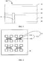
- an array antenna 100 provided in an implementation manner of the present invention includes a first metal layer 10, a first dielectric layer 40, a second metal layer 20, a second dielectric layer 50 and a third metal layer 30 that are sequentially laminated, where multiple metal through holes 51 are disposed on the second dielectric layer 50, the multiple metal through holes 51 are electrically connected between the second metal layer 20 and the third metal layer 30, and form a feeding section 52.
- the multiple metal through holes 51 run through the second metal layer 20, the second dielectric layer 50 and the third metal layer 30, and form the feeding section 52.
- the multiple metal through holes 51 may also be embedded in the second dielectric layer 50, and electrically connected to the second metal layer 20 and the third metal layer 30 in a physical connection manner.
- the first metal layer 10 includes multiple subarrays 11, each subarray 11 includes multiple radiating arrays 111 and one power splitter 112, the power splitter 112 includes a central area 1122 and multiple branches 1124 extending from the central area, and the multiple radiating arrays 111 are respectively connected to ends of the multiple branches 1124 that are far from the central area 1122 to form a parallel signal transmission architecture.
- Multiple coupling slots 21 are disposed on the second metal layer 20, and the multiple coupling slots 21 respectively face central areas 1122 of the multiple power splitters 112.
- the feeding section 52 is used to feed a signal, the signal is transmitted to the central areas 1122 of the power splitters 112 by using the multiple coupling slots 21, and the signal is transmitted to the multiple radiating arrays 111 by using the multiple branches 1124.
- bandwidth of the array antenna 100 is increased, and a high-gain compact-broadband planar millimeter wave array antenna 100 is provided.
- the multiple metal through holes 51 are disposed on the second dielectric layer 50, and the multiple metal through holes 51 form the feeding section 52 together.
- a transmission line structure having a small loss is used to feed the array antenna 100, and there are multiple signal feeding manners for the feeding section 52 of the array antenna 100 in the present invention, which mainly depends on a transmission line design of a circuit connected to the array antenna 100.
- a transmission line of the feeding section 52 is a substrate-integrated waveguide, and there are multiple transmission line conversion manners that can connect the substrate-integrated waveguide to a transmission line, such as a waveguide, a microstrip, and a coplanar waveguide, to implement signal feeding for the array antenna 100. Referring to FIG. 8 to FIG.
- FIG. 8 is a tapered transition structure.
- FIG. 9 is a probe transition structure.
- FIG. 10 is a coplanar waveguide transition structure based on a substrate-integrated waveguide (SIW).
- the multiple subarrays 11 in the present invention are distributed in the first metal layer 10 covering a surface of the first dielectric layer 40.
- a circuit structure of the multiple subarrays 11 is formed by using a method, such as etching the first metal layer 10.
- the subarray 11 in the present invention is a surface mount array of a planar structure, and is formed by a microstrip.
- the present invention can ensure a planar structure, and also implement highly efficient feeding and radiation.
- the array antenna 100 provided in the present invention implements feeding and radiation in a shunt-fed manner, and in large array application, it can be ensured that a broadband property of the array antenna is not changed. Because the array antenna 100 provided in the present invention uses parallel feeding, which ensures that paths from a feed port to all the subarrays 11 are consistent, even though a signal frequency changes, phases of signals reaching the subarrays 11 are still consistent, so that performance of the array antenna 100 is kept, and a contradiction between broadband work and a requirement for a high gain is resolved.
- the array antenna 100 is processed by using a standard multilayer circuit board manufacturing technology, which facilitates mass production and has high reliability and a high repetition rate.
- the first metal layer 10, the first dielectric layer 40 and the second metal layer 20 are considered as a first substrate with two sides coated with copper
- the second metal layer 20, the second dielectric layer 50 and the second metal layer 30 are considered as a second substrate with two sides coated with copper
- the first substrate and the second substrate form an architecture in which the first metal layer 10, the first dielectric layer 40, the second metal layer 20, the second dielectric layer 50, and the third metal layer 30 are sequentially laminated.
- the second metal layer of the first substrate and the second metal layer of the second substrate overlap and are press-fitted into one layer.
- the feeding section 52 of the array antenna in the present invention is right under the subarrays 11, which implements array miniaturization and reduces space.
- the multiple subarrays 11 in the present invention are 2x2 arrays. In another implementation manner, the multiple subarrays 11 may also be N ⁇ N arrays, where N is a natural number.
- the feeding section 52 includes multiple feeding units 54, and projections of the multiple coupling slots 21 on the second dielectric layer 50 respectively fall within ranges of the multiple feeding units 54.
- the multiple coupling slots 21 are perpendicular to the second metal layer 20 and the second dielectric layer 50.
- each of the feeding units 54 is of a mirror symmetric structure
- metal through holes 51 forming the feeding unit 54 are symmetrically distributed on two sides of a central line A of the feeding unit 54
- the multiple coupling slots 21 deviate from central lines A of the corresponding feeding units 54, to split a surface current.
- Electromagnetic waves of the feeding section 52 are coupled to the central areas 1122 of the power splitters 112 by using the coupling slots 21.
- the branches 1124 and the central area 1122 of the power splitter 112 form a transmission structure distributed back to back, and the multiple branches 1124 are symmetrically distributed on two sides of the central area 1122. Because the coupling slots 21 and the central areas 1122 overlap, directions of electric fields on branches 1124 that are symmetric relative to the coupling slots 21 are reverse.
- Each of the feeding units 54 includes a pair of transmission portions 56, a short-circuit end 58, and an open end 59, where the short-circuit end 58 is connected between the pair of transmission portions 56 and is located on one end of the pair of transmission portions 56, the open end 59 is located on one side of the transmission portions 56 that is far from the short-circuit end 58, each two of the multiple feeding units 54 are opposite to each other, and open ends 59 of the two feeding units 54 that are opposite to each other are adjacent to each other. In this implementation manner, the transmission portions 56 are parallel to each other.
- Each feeding unit 54 is formed by arranged metal through holes 51.
- each transmission portion is formed by four metal through holes arranged in a straight line
- the short-circuit end is formed by two metal through holes
- the two metal through holes 51 forming the short-circuit end 58 are connected between one pair of transmission portions 56, thereby forming a substrate-integrated waveguide having a closed end.
- a length of the coupling slot 21 is a half of a wavelength of a center frequency of the antenna 100, and a distance between the coupling slot 21 and the short-circuit end 58 is a quarter of the wavelength of the center frequency.
- Performance of the antenna is related to a frequency. Generally, a frequency at which the antenna has best performance is referred to as a center frequency. When a frequency is deviated from this frequency, no matter the frequency becomes lower or higher, the antenna performance is lowered, a principle of which is that composition structures in the antenna, such as a transmission line, a transmission line conversion structure, and a structure and size of a radiating unit, are related to the signal frequency.
- a center frequency needs to be set according to an actual requirement, and is used as a design input to design composition parts of the antenna, and in solutions of designing the antenna and the composition parts of the antenna, a solution in which performance is slowly lowered in the case of deviation from the center frequency is considered as far as possible.
- the feeding section 52 further includes a T-shaped power splitter 55, where the T-shaped power splitter 55 is located between two adjacent feeding units 54, and is close to open ends 59 of the feeding units 54.
- the T-shaped power splitter 55 functions to split one channel of signal into two channels.
- each T-shaped power splitter 55 is formed by three metal through holes 51 that are triangularly arranged.
- the multiple branches 1124 are symmetrically distributed on two sides of the central area 1122, and the radiating arrays 111 are symmetrically distributed on two sides of the power splitter 112.
- the first dielectric layer 40 and the first metal layer 10 form a radiating dielectric substrate of the array antenna 100
- the second metal layer 20, the second dielectric layer 50 and the third metal layer 30 together form a feeding dielectric substrate of the array antenna 100, and thicknesses and dielectric constants of the radiating dielectric substrate and the feeding dielectric substrate are different.
- the thickness and the dielectric constant of the radiating dielectric substrate may be selected according to design requirement of feeding and radiation of the array antenna, and the thickness and the dielectric constant of the feeding dielectric substrate may be selected according to a convenience degree of integration with an active circuit. Selection can be performed flexibly, which helps ensure bandwidth and a gain of the array antenna 100.
- the radiating dielectric substrate and the feeding dielectric substrate overlap.
- the thickness of the radiating dielectric substrate is 0.254 mm
- the thickness of the feeding dielectric substrate is 0.508 mm.
- the multiple coupling slots 21 are rectangular, the multiple metal through holes 51 are circular, and the multiple radiating arrays 111 are square.
- the power splitter 112 is a microstrip splitter, and is of a planar structure, so that the array antenna 100 has a compact structure and a small size.
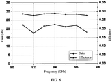
- FIG. 6 is a line graph of a relationship between a gain, an efficiency and a frequency of the array antenna 100 according to the present invention.
- a frequency of the array antenna 100 is within a range of 90 GHz to 98 GHz, a gain that is achieved is within a range of 27.7 dBi to 28.8 dBi, a relative bandwidth is up to 9.5%, and an efficiency of the array antenna 100 is within a range of 0.18 to 0.22.
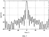
- FIG. 7 is a diagram of an emulated radiation direction of an array antenna according to the present invention. It can be known from the figure that the array antenna 100 achieves a high gain and a low side lobe level of -12.8 dB.
Landscapes
- Engineering & Computer Science (AREA)
- Manufacturing & Machinery (AREA)
- Variable-Direction Aerials And Aerial Arrays (AREA)
- Waveguide Aerials (AREA)
Priority Applications (1)
| Application Number | Priority Date | Filing Date | Title |
|---|---|---|---|
| EP18179805.9A EP3462543B1 (en) | 2014-03-12 | 2014-03-12 | Array antenna |
Applications Claiming Priority (3)
| Application Number | Priority Date | Filing Date | Title |
|---|---|---|---|
| PCT/CN2014/073269 WO2015135153A1 (zh) | 2014-03-12 | 2014-03-12 | 阵列天线 |
| EP14885247.8A EP3109942B1 (en) | 2014-03-12 | 2014-03-12 | Array antenna |
| EP18179805.9A EP3462543B1 (en) | 2014-03-12 | 2014-03-12 | Array antenna |
Related Parent Applications (1)
| Application Number | Title | Priority Date | Filing Date |
|---|---|---|---|
| EP14885247.8A Division EP3109942B1 (en) | 2014-03-12 | 2014-03-12 | Array antenna |
Publications (2)
| Publication Number | Publication Date |
|---|---|
| EP3462543A1 EP3462543A1 (en) | 2019-04-03 |
| EP3462543B1 true EP3462543B1 (en) | 2021-05-05 |
Family
ID=54070792
Family Applications (2)
| Application Number | Title | Priority Date | Filing Date |
|---|---|---|---|
| EP14885247.8A Active EP3109942B1 (en) | 2014-03-12 | 2014-03-12 | Array antenna |
| EP18179805.9A Active EP3462543B1 (en) | 2014-03-12 | 2014-03-12 | Array antenna |
Family Applications Before (1)
| Application Number | Title | Priority Date | Filing Date |
|---|---|---|---|
| EP14885247.8A Active EP3109942B1 (en) | 2014-03-12 | 2014-03-12 | Array antenna |
Country Status (5)
| Country | Link |
|---|---|
| US (1) | US10199743B2 (zh) |
| EP (2) | EP3109942B1 (zh) |
| CN (1) | CN105190998B (zh) |
| ES (1) | ES2687289T3 (zh) |
| WO (1) | WO2015135153A1 (zh) |
Families Citing this family (20)
| Publication number | Priority date | Publication date | Assignee | Title |
|---|---|---|---|---|
| CN106450762B (zh) * | 2016-10-19 | 2023-10-10 | 厦门致联科技有限公司 | 一种紧凑的对称馈电网络 |
| CN109478716B (zh) * | 2016-12-30 | 2020-08-25 | 华为技术有限公司 | 天线 |
| FR3064408B1 (fr) * | 2017-03-23 | 2019-04-26 | Thales | Antenne electromagnetique |
| CN107196049B (zh) * | 2017-06-15 | 2023-03-17 | 东南大学 | 一种阵列天线 |
| CN109494488A (zh) * | 2017-09-12 | 2019-03-19 | 湘南学院 | 一种高效低剖面大规模圆极化阵列天线 |
| CN109494457A (zh) * | 2017-09-12 | 2019-03-19 | 湘南学院 | 一种高效低剖面宽轴比带宽大规模圆极化阵列天线 |
| JP6533560B2 (ja) * | 2017-09-21 | 2019-06-19 | 株式会社フジクラ | アンテナ装置 |
| JP2019057832A (ja) * | 2017-09-21 | 2019-04-11 | 株式会社フジクラ | アンテナ装置 |
| CN108232437B (zh) * | 2017-12-20 | 2024-03-15 | 华南理工大学 | 一种锥形波束宽带缝隙天线阵列及头戴vr设备 |
| JP2019140644A (ja) * | 2018-02-15 | 2019-08-22 | パナソニック株式会社 | アンテナ装置 |
| CN108777349B (zh) * | 2018-04-28 | 2024-04-05 | 江西省仁富电子科技有限公司 | 一种一体式多流阵列天线 |
| US10854991B2 (en) * | 2018-07-06 | 2020-12-01 | City University Of Hong Kong | Waveguide fed open slot antenna |
| CN109103605A (zh) * | 2018-08-07 | 2018-12-28 | 北京凌波微步信息技术有限公司 | 一种采用倒置微带缝隙波导馈电的阵列天线 |
| CN112448174B (zh) * | 2019-09-04 | 2024-05-03 | 中国移动通信集团终端有限公司 | 天线系统和终端设备 |
| CN111244619A (zh) * | 2019-12-13 | 2020-06-05 | 南京理工大学 | 基于空气基片集成波导的贴片阵列天线 |
| CN111244624B (zh) * | 2020-03-12 | 2022-07-08 | 南京航空航天大学 | 一种基片集成波导馈电的寄生贴片阵列天线 |
| CN111244608A (zh) * | 2020-03-13 | 2020-06-05 | 上海几何伙伴智能驾驶有限公司 | 低副瓣雷达天线及车载雷达天线 |
| CN116325364A (zh) * | 2020-09-28 | 2023-06-23 | 华为技术有限公司 | 一种天线阵列、装置及无线通信设备 |
| CN113067134B (zh) * | 2021-03-30 | 2022-09-13 | 苏州沙岸通信科技有限公司 | 适用于cpe及室内微基站的5g阵列天线 |
| CN114914687A (zh) * | 2022-05-12 | 2022-08-16 | 华南理工大学 | 一种天线单元、子阵及毫米波高隔离大角度相控阵列天线 |
Family Cites Families (9)
| Publication number | Priority date | Publication date | Assignee | Title |
|---|---|---|---|---|
| DE69823591T2 (de) * | 1997-07-25 | 2005-04-07 | Kyocera Corp. | Geschichtete Aperturantenne und mehrschichtige Leiterplatte damit |
| JP4323413B2 (ja) * | 2004-11-05 | 2009-09-02 | 新光電気工業株式会社 | パッチアンテナ、アレイアンテナおよびそれを備えた実装基板 |
| CN1885616A (zh) * | 2005-06-23 | 2006-12-27 | 北京海域天华通讯设备有限公司 | 高增益波导喇叭阵列平板天线 |
| US7808439B2 (en) * | 2007-09-07 | 2010-10-05 | University Of Tennessee Reserch Foundation | Substrate integrated waveguide antenna array |
| KR101067118B1 (ko) * | 2009-12-08 | 2011-09-22 | 고려대학교 산학협력단 | 다층 기판에 내장된 유전체 공진기 안테나 |
| KR101055425B1 (ko) * | 2010-04-30 | 2011-08-08 | 삼성전기주식회사 | 광대역 전송선로-도파관 변환장치 |
| CN102110902A (zh) * | 2011-03-03 | 2011-06-29 | 北京星正通信技术有限责任公司 | 圆极化平板天线 |
| US8558746B2 (en) * | 2011-11-16 | 2013-10-15 | Andrew Llc | Flat panel array antenna |
| CN103268981A (zh) * | 2013-05-14 | 2013-08-28 | 中国科学院深圳先进技术研究院 | 一种基片集成波导开槽耦合馈电的平面贴片天线 |
-
2014
- 2014-03-12 EP EP14885247.8A patent/EP3109942B1/en active Active
- 2014-03-12 ES ES14885247.8T patent/ES2687289T3/es active Active
- 2014-03-12 CN CN201480000131.8A patent/CN105190998B/zh active Active
- 2014-03-12 WO PCT/CN2014/073269 patent/WO2015135153A1/zh active Application Filing
- 2014-03-12 EP EP18179805.9A patent/EP3462543B1/en active Active
-
2016
- 2016-09-09 US US15/261,006 patent/US10199743B2/en active Active
Also Published As
| Publication number | Publication date |
|---|---|
| EP3109942A4 (en) | 2017-03-01 |
| US20160380362A1 (en) | 2016-12-29 |
| CN105190998B (zh) | 2017-12-01 |
| WO2015135153A1 (zh) | 2015-09-17 |
| EP3109942A1 (en) | 2016-12-28 |
| ES2687289T3 (es) | 2018-10-24 |
| US10199743B2 (en) | 2019-02-05 |
| CN105190998A (zh) | 2015-12-23 |
| EP3109942B1 (en) | 2018-07-25 |
| EP3462543A1 (en) | 2019-04-03 |
Similar Documents
| Publication | Publication Date | Title |
|---|---|---|
| US10199743B2 (en) | Array antenna | |
| Cheng et al. | W-band large-scale high-gain planar integrated antenna array | |
| US10741914B2 (en) | Planar ultrawideband modular antenna array having improved bandwidth | |
| JP6129857B2 (ja) | 偏波共用アンテナ | |
| US9000996B2 (en) | Modular wideband antenna array | |
| JP4856078B2 (ja) | 反射アンテナ | |
| JP2020532891A (ja) | 移行装置、移行構造、及び、集積パッケージ構造 | |
| CN107492713B (zh) | 一种双圆极化阵列天线 | |
| Kim et al. | A Series Slot Array Antenna for 45$^{\circ} $-Inclined Linear Polarization With SIW Technology | |
| US10361485B2 (en) | Tripole current loop radiating element with integrated circularly polarized feed | |
| CN107819201B (zh) | 一种适用于5g毫米波通信的紧凑型渐变缝隙阵列天线 | |
| EP2948999B1 (en) | Dipole antenna array | |
| TWI600209B (zh) | Antenna reset circuit | |
| EP3972057A1 (en) | Dual polarized antenna using shift series feed | |
| US9865936B2 (en) | Array antenna feed structures | |
| Aziz et al. | High gain compact 57-66 GHz antenna array for backhaul & access communications | |
| CN114336020B (zh) | 一种基于不对称开槽矩形贴片的宽带圆极化天线阵列 | |
| CN219040732U (zh) | 一种双圆极化阵列天线 | |
| Chen et al. | Bandwidth enhancement of substrate integrated waveguide (SIW) slot antenna with parasitic dipole | |
| Banerjee et al. | An Integrated, Phase-Controlled Power Divider for Metasurface Array Antennas | |
| Kumar et al. | Design of bulk micro-machined patch antenna arrays for earth exploration satellite services | |
| Muriel-Barrado et al. | An Electrical-Contactless Substrate-Over-Waveguide Planar Array Slot Antenna | |
| Slomian et al. | Dual polarized two-port antenna lattice | |
| Erfani et al. | A 60‐GH z multi‐beam antenna array design by using MHMICs technology | |
| Duan et al. | Wideband Design of a Single-Layer Corporate-Fed Substrate Integrated Waveguide Slot Subarray |
Legal Events
| Date | Code | Title | Description |
|---|---|---|---|
| PUAI | Public reference made under article 153(3) epc to a published international application that has entered the european phase |
Free format text: ORIGINAL CODE: 0009012 |
|
| STAA | Information on the status of an ep patent application or granted ep patent |
Free format text: STATUS: REQUEST FOR EXAMINATION WAS MADE |
|
| 17P | Request for examination filed |
Effective date: 20180626 |
|
| AC | Divisional application: reference to earlier application |
Ref document number: 3109942 Country of ref document: EP Kind code of ref document: P |
|
| AK | Designated contracting states |
Kind code of ref document: A1 Designated state(s): AL AT BE BG CH CY CZ DE DK EE ES FI FR GB GR HR HU IE IS IT LI LT LU LV MC MK MT NL NO PL PT RO RS SE SI SK SM TR |
|
| GRAP | Despatch of communication of intention to grant a patent |
Free format text: ORIGINAL CODE: EPIDOSNIGR1 |
|
| STAA | Information on the status of an ep patent application or granted ep patent |
Free format text: STATUS: GRANT OF PATENT IS INTENDED |
|
| INTG | Intention to grant announced |
Effective date: 20201109 |
|
| GRAS | Grant fee paid |
Free format text: ORIGINAL CODE: EPIDOSNIGR3 |
|
| GRAA | (expected) grant |
Free format text: ORIGINAL CODE: 0009210 |
|
| STAA | Information on the status of an ep patent application or granted ep patent |
Free format text: STATUS: THE PATENT HAS BEEN GRANTED |
|
| AC | Divisional application: reference to earlier application |
Ref document number: 3109942 Country of ref document: EP Kind code of ref document: P |
|
| AK | Designated contracting states |
Kind code of ref document: B1 Designated state(s): AL AT BE BG CH CY CZ DE DK EE ES FI FR GB GR HR HU IE IS IT LI LT LU LV MC MK MT NL NO PL PT RO RS SE SI SK SM TR |
|
| REG | Reference to a national code |
Ref country code: GB Ref legal event code: FG4D |
|
| REG | Reference to a national code |
Ref country code: CH Ref legal event code: EP |
|
| REG | Reference to a national code |
Ref country code: AT Ref legal event code: REF Ref document number: 1390987 Country of ref document: AT Kind code of ref document: T Effective date: 20210515 |
|
| REG | Reference to a national code |
Ref country code: IE Ref legal event code: FG4D |
|
| REG | Reference to a national code |
Ref country code: DE Ref legal event code: R096 Ref document number: 602014077339 Country of ref document: DE |
|
| REG | Reference to a national code |
Ref country code: LT Ref legal event code: MG9D |
|
| REG | Reference to a national code |
Ref country code: AT Ref legal event code: MK05 Ref document number: 1390987 Country of ref document: AT Kind code of ref document: T Effective date: 20210505 |
|
| PG25 | Lapsed in a contracting state [announced via postgrant information from national office to epo] |
Ref country code: AT Free format text: LAPSE BECAUSE OF FAILURE TO SUBMIT A TRANSLATION OF THE DESCRIPTION OR TO PAY THE FEE WITHIN THE PRESCRIBED TIME-LIMIT Effective date: 20210505 Ref country code: BG Free format text: LAPSE BECAUSE OF FAILURE TO SUBMIT A TRANSLATION OF THE DESCRIPTION OR TO PAY THE FEE WITHIN THE PRESCRIBED TIME-LIMIT Effective date: 20210805 Ref country code: FI Free format text: LAPSE BECAUSE OF FAILURE TO SUBMIT A TRANSLATION OF THE DESCRIPTION OR TO PAY THE FEE WITHIN THE PRESCRIBED TIME-LIMIT Effective date: 20210505 Ref country code: HR Free format text: LAPSE BECAUSE OF FAILURE TO SUBMIT A TRANSLATION OF THE DESCRIPTION OR TO PAY THE FEE WITHIN THE PRESCRIBED TIME-LIMIT Effective date: 20210505 Ref country code: LT Free format text: LAPSE BECAUSE OF FAILURE TO SUBMIT A TRANSLATION OF THE DESCRIPTION OR TO PAY THE FEE WITHIN THE PRESCRIBED TIME-LIMIT Effective date: 20210505 |
|
| PG25 | Lapsed in a contracting state [announced via postgrant information from national office to epo] |
Ref country code: NO Free format text: LAPSE BECAUSE OF FAILURE TO SUBMIT A TRANSLATION OF THE DESCRIPTION OR TO PAY THE FEE WITHIN THE PRESCRIBED TIME-LIMIT Effective date: 20210805 Ref country code: LV Free format text: LAPSE BECAUSE OF FAILURE TO SUBMIT A TRANSLATION OF THE DESCRIPTION OR TO PAY THE FEE WITHIN THE PRESCRIBED TIME-LIMIT Effective date: 20210505 Ref country code: PL Free format text: LAPSE BECAUSE OF FAILURE TO SUBMIT A TRANSLATION OF THE DESCRIPTION OR TO PAY THE FEE WITHIN THE PRESCRIBED TIME-LIMIT Effective date: 20210505 Ref country code: PT Free format text: LAPSE BECAUSE OF FAILURE TO SUBMIT A TRANSLATION OF THE DESCRIPTION OR TO PAY THE FEE WITHIN THE PRESCRIBED TIME-LIMIT Effective date: 20210906 Ref country code: SE Free format text: LAPSE BECAUSE OF FAILURE TO SUBMIT A TRANSLATION OF THE DESCRIPTION OR TO PAY THE FEE WITHIN THE PRESCRIBED TIME-LIMIT Effective date: 20210505 Ref country code: RS Free format text: LAPSE BECAUSE OF FAILURE TO SUBMIT A TRANSLATION OF THE DESCRIPTION OR TO PAY THE FEE WITHIN THE PRESCRIBED TIME-LIMIT Effective date: 20210505 Ref country code: GR Free format text: LAPSE BECAUSE OF FAILURE TO SUBMIT A TRANSLATION OF THE DESCRIPTION OR TO PAY THE FEE WITHIN THE PRESCRIBED TIME-LIMIT Effective date: 20210806 Ref country code: IS Free format text: LAPSE BECAUSE OF FAILURE TO SUBMIT A TRANSLATION OF THE DESCRIPTION OR TO PAY THE FEE WITHIN THE PRESCRIBED TIME-LIMIT Effective date: 20210905 |
|
| REG | Reference to a national code |
Ref country code: NL Ref legal event code: MP Effective date: 20210505 |
|
| PG25 | Lapsed in a contracting state [announced via postgrant information from national office to epo] |
Ref country code: NL Free format text: LAPSE BECAUSE OF FAILURE TO SUBMIT A TRANSLATION OF THE DESCRIPTION OR TO PAY THE FEE WITHIN THE PRESCRIBED TIME-LIMIT Effective date: 20210505 |
|
| PG25 | Lapsed in a contracting state [announced via postgrant information from national office to epo] |
Ref country code: DK Free format text: LAPSE BECAUSE OF FAILURE TO SUBMIT A TRANSLATION OF THE DESCRIPTION OR TO PAY THE FEE WITHIN THE PRESCRIBED TIME-LIMIT Effective date: 20210505 Ref country code: CZ Free format text: LAPSE BECAUSE OF FAILURE TO SUBMIT A TRANSLATION OF THE DESCRIPTION OR TO PAY THE FEE WITHIN THE PRESCRIBED TIME-LIMIT Effective date: 20210505 Ref country code: RO Free format text: LAPSE BECAUSE OF FAILURE TO SUBMIT A TRANSLATION OF THE DESCRIPTION OR TO PAY THE FEE WITHIN THE PRESCRIBED TIME-LIMIT Effective date: 20210505 Ref country code: EE Free format text: LAPSE BECAUSE OF FAILURE TO SUBMIT A TRANSLATION OF THE DESCRIPTION OR TO PAY THE FEE WITHIN THE PRESCRIBED TIME-LIMIT Effective date: 20210505 Ref country code: ES Free format text: LAPSE BECAUSE OF FAILURE TO SUBMIT A TRANSLATION OF THE DESCRIPTION OR TO PAY THE FEE WITHIN THE PRESCRIBED TIME-LIMIT Effective date: 20210505 Ref country code: SK Free format text: LAPSE BECAUSE OF FAILURE TO SUBMIT A TRANSLATION OF THE DESCRIPTION OR TO PAY THE FEE WITHIN THE PRESCRIBED TIME-LIMIT Effective date: 20210505 Ref country code: SM Free format text: LAPSE BECAUSE OF FAILURE TO SUBMIT A TRANSLATION OF THE DESCRIPTION OR TO PAY THE FEE WITHIN THE PRESCRIBED TIME-LIMIT Effective date: 20210505 |
|
| REG | Reference to a national code |
Ref country code: DE Ref legal event code: R097 Ref document number: 602014077339 Country of ref document: DE |
|
| PLBE | No opposition filed within time limit |
Free format text: ORIGINAL CODE: 0009261 |
|
| STAA | Information on the status of an ep patent application or granted ep patent |
Free format text: STATUS: NO OPPOSITION FILED WITHIN TIME LIMIT |
|
| 26N | No opposition filed |
Effective date: 20220208 |
|
| PG25 | Lapsed in a contracting state [announced via postgrant information from national office to epo] |
Ref country code: IS Free format text: LAPSE BECAUSE OF FAILURE TO SUBMIT A TRANSLATION OF THE DESCRIPTION OR TO PAY THE FEE WITHIN THE PRESCRIBED TIME-LIMIT Effective date: 20210905 Ref country code: AL Free format text: LAPSE BECAUSE OF FAILURE TO SUBMIT A TRANSLATION OF THE DESCRIPTION OR TO PAY THE FEE WITHIN THE PRESCRIBED TIME-LIMIT Effective date: 20210505 |
|
| PG25 | Lapsed in a contracting state [announced via postgrant information from national office to epo] |
Ref country code: IT Free format text: LAPSE BECAUSE OF FAILURE TO SUBMIT A TRANSLATION OF THE DESCRIPTION OR TO PAY THE FEE WITHIN THE PRESCRIBED TIME-LIMIT Effective date: 20210505 |
|
| REG | Reference to a national code |
Ref country code: DE Ref legal event code: R119 Ref document number: 602014077339 Country of ref document: DE |
|
| PG25 | Lapsed in a contracting state [announced via postgrant information from national office to epo] |
Ref country code: MC Free format text: LAPSE BECAUSE OF FAILURE TO SUBMIT A TRANSLATION OF THE DESCRIPTION OR TO PAY THE FEE WITHIN THE PRESCRIBED TIME-LIMIT Effective date: 20210505 |
|
| REG | Reference to a national code |
Ref country code: CH Ref legal event code: PL |
|
| GBPC | Gb: european patent ceased through non-payment of renewal fee |
Effective date: 20220312 |
|
| REG | Reference to a national code |
Ref country code: BE Ref legal event code: MM Effective date: 20220331 |
|
| PG25 | Lapsed in a contracting state [announced via postgrant information from national office to epo] |
Ref country code: LU Free format text: LAPSE BECAUSE OF NON-PAYMENT OF DUE FEES Effective date: 20220312 Ref country code: LI Free format text: LAPSE BECAUSE OF NON-PAYMENT OF DUE FEES Effective date: 20220331 Ref country code: IE Free format text: LAPSE BECAUSE OF NON-PAYMENT OF DUE FEES Effective date: 20220312 Ref country code: GB Free format text: LAPSE BECAUSE OF NON-PAYMENT OF DUE FEES Effective date: 20220312 Ref country code: DE Free format text: LAPSE BECAUSE OF NON-PAYMENT OF DUE FEES Effective date: 20221001 Ref country code: CH Free format text: LAPSE BECAUSE OF NON-PAYMENT OF DUE FEES Effective date: 20220331 |
|
| PG25 | Lapsed in a contracting state [announced via postgrant information from national office to epo] |
Ref country code: BE Free format text: LAPSE BECAUSE OF NON-PAYMENT OF DUE FEES Effective date: 20220331 |
|
| PGFP | Annual fee paid to national office [announced via postgrant information from national office to epo] |
Ref country code: FR Payment date: 20230208 Year of fee payment: 10 |
|
| PG25 | Lapsed in a contracting state [announced via postgrant information from national office to epo] |
Ref country code: HU Free format text: LAPSE BECAUSE OF FAILURE TO SUBMIT A TRANSLATION OF THE DESCRIPTION OR TO PAY THE FEE WITHIN THE PRESCRIBED TIME-LIMIT; INVALID AB INITIO Effective date: 20140312 |
|
| PG25 | Lapsed in a contracting state [announced via postgrant information from national office to epo] |
Ref country code: MK Free format text: LAPSE BECAUSE OF FAILURE TO SUBMIT A TRANSLATION OF THE DESCRIPTION OR TO PAY THE FEE WITHIN THE PRESCRIBED TIME-LIMIT Effective date: 20210505 Ref country code: CY Free format text: LAPSE BECAUSE OF FAILURE TO SUBMIT A TRANSLATION OF THE DESCRIPTION OR TO PAY THE FEE WITHIN THE PRESCRIBED TIME-LIMIT Effective date: 20210505 |