EP3462533A1 - Low-loss plug connection arrangement and system having at least one such plug connection arrangement - Google Patents
Low-loss plug connection arrangement and system having at least one such plug connection arrangement Download PDFInfo
- Publication number
- EP3462533A1 EP3462533A1 EP18196896.7A EP18196896A EP3462533A1 EP 3462533 A1 EP3462533 A1 EP 3462533A1 EP 18196896 A EP18196896 A EP 18196896A EP 3462533 A1 EP3462533 A1 EP 3462533A1
- Authority
- EP
- European Patent Office
- Prior art keywords
- plug connection
- radiation source
- connection arrangement
- dielectric waveguide
- housing
- Prior art date
- Legal status (The legal status is an assumption and is not a legal conclusion. Google has not performed a legal analysis and makes no representation as to the accuracy of the status listed.)
- Granted
Links
Images




Classifications
-
- H—ELECTRICITY
- H01—ELECTRIC ELEMENTS
- H01Q—ANTENNAS, i.e. RADIO AERIALS
- H01Q1/00—Details of, or arrangements associated with, antennas
- H01Q1/50—Structural association of antennas with earthing switches, lead-in devices or lightning protectors
-
- H—ELECTRICITY
- H01—ELECTRIC ELEMENTS
- H01P—WAVEGUIDES; RESONATORS, LINES, OR OTHER DEVICES OF THE WAVEGUIDE TYPE
- H01P5/00—Coupling devices of the waveguide type
- H01P5/08—Coupling devices of the waveguide type for linking dissimilar lines or devices
-
- H—ELECTRICITY
- H01—ELECTRIC ELEMENTS
- H01P—WAVEGUIDES; RESONATORS, LINES, OR OTHER DEVICES OF THE WAVEGUIDE TYPE
- H01P3/00—Waveguides; Transmission lines of the waveguide type
- H01P3/16—Dielectric waveguides, i.e. without a longitudinal conductor
-
- G—PHYSICS
- G02—OPTICS
- G02B—OPTICAL ELEMENTS, SYSTEMS OR APPARATUS
- G02B6/00—Light guides; Structural details of arrangements comprising light guides and other optical elements, e.g. couplings
- G02B6/24—Coupling light guides
- G02B6/36—Mechanical coupling means
- G02B6/38—Mechanical coupling means having fibre to fibre mating means
-
- H—ELECTRICITY
- H01—ELECTRIC ELEMENTS
- H01P—WAVEGUIDES; RESONATORS, LINES, OR OTHER DEVICES OF THE WAVEGUIDE TYPE
- H01P5/00—Coupling devices of the waveguide type
- H01P5/08—Coupling devices of the waveguide type for linking dissimilar lines or devices
- H01P5/087—Transitions to a dielectric waveguide
-
- H—ELECTRICITY
- H01—ELECTRIC ELEMENTS
- H01P—WAVEGUIDES; RESONATORS, LINES, OR OTHER DEVICES OF THE WAVEGUIDE TYPE
- H01P5/00—Coupling devices of the waveguide type
- H01P5/12—Coupling devices having more than two ports
- H01P5/16—Conjugate devices, i.e. devices having at least one port decoupled from one other port
- H01P5/18—Conjugate devices, i.e. devices having at least one port decoupled from one other port consisting of two coupled guides, e.g. directional couplers
-
- H—ELECTRICITY
- H01—ELECTRIC ELEMENTS
- H01Q—ANTENNAS, i.e. RADIO AERIALS
- H01Q13/00—Waveguide horns or mouths; Slot antennas; Leaky-waveguide antennas; Equivalent structures causing radiation along the transmission path of a guided wave
- H01Q13/20—Non-resonant leaky-waveguide or transmission-line antennas; Equivalent structures causing radiation along the transmission path of a guided wave
-
- H—ELECTRICITY
- H01—ELECTRIC ELEMENTS
- H01Q—ANTENNAS, i.e. RADIO AERIALS
- H01Q19/00—Combinations of primary active antenna elements and units with secondary devices, e.g. with quasi-optical devices, for giving the antenna a desired directional characteristic
- H01Q19/28—Combinations of primary active antenna elements and units with secondary devices, e.g. with quasi-optical devices, for giving the antenna a desired directional characteristic using a secondary device in the form of two or more substantially straight conductive elements
- H01Q19/30—Combinations of primary active antenna elements and units with secondary devices, e.g. with quasi-optical devices, for giving the antenna a desired directional characteristic using a secondary device in the form of two or more substantially straight conductive elements the primary active element being centre-fed and substantially straight, e.g. Yagi antenna
-
- H—ELECTRICITY
- H01—ELECTRIC ELEMENTS
- H01R—ELECTRICALLY-CONDUCTIVE CONNECTIONS; STRUCTURAL ASSOCIATIONS OF A PLURALITY OF MUTUALLY-INSULATED ELECTRICAL CONNECTING ELEMENTS; COUPLING DEVICES; CURRENT COLLECTORS
- H01R12/00—Structural associations of a plurality of mutually-insulated electrical connecting elements, specially adapted for printed circuits, e.g. printed circuit boards [PCB], flat or ribbon cables, or like generally planar structures, e.g. terminal strips, terminal blocks; Coupling devices specially adapted for printed circuits, flat or ribbon cables, or like generally planar structures; Terminals specially adapted for contact with, or insertion into, printed circuits, flat or ribbon cables, or like generally planar structures
-
- H—ELECTRICITY
- H01—ELECTRIC ELEMENTS
- H01R—ELECTRICALLY-CONDUCTIVE CONNECTIONS; STRUCTURAL ASSOCIATIONS OF A PLURALITY OF MUTUALLY-INSULATED ELECTRICAL CONNECTING ELEMENTS; COUPLING DEVICES; CURRENT COLLECTORS
- H01R12/00—Structural associations of a plurality of mutually-insulated electrical connecting elements, specially adapted for printed circuits, e.g. printed circuit boards [PCB], flat or ribbon cables, or like generally planar structures, e.g. terminal strips, terminal blocks; Coupling devices specially adapted for printed circuits, flat or ribbon cables, or like generally planar structures; Terminals specially adapted for contact with, or insertion into, printed circuits, flat or ribbon cables, or like generally planar structures
- H01R12/70—Coupling devices
- H01R12/71—Coupling devices for rigid printing circuits or like structures
- H01R12/72—Coupling devices for rigid printing circuits or like structures coupling with the edge of the rigid printed circuits or like structures
-
- H—ELECTRICITY
- H01—ELECTRIC ELEMENTS
- H01R—ELECTRICALLY-CONDUCTIVE CONNECTIONS; STRUCTURAL ASSOCIATIONS OF A PLURALITY OF MUTUALLY-INSULATED ELECTRICAL CONNECTING ELEMENTS; COUPLING DEVICES; CURRENT COLLECTORS
- H01R24/00—Two-part coupling devices, or either of their cooperating parts, characterised by their overall structure
- H01R24/38—Two-part coupling devices, or either of their cooperating parts, characterised by their overall structure having concentrically or coaxially arranged contacts
- H01R24/40—Two-part coupling devices, or either of their cooperating parts, characterised by their overall structure having concentrically or coaxially arranged contacts specially adapted for high frequency
- H01R24/50—Two-part coupling devices, or either of their cooperating parts, characterised by their overall structure having concentrically or coaxially arranged contacts specially adapted for high frequency mounted on a PCB [Printed Circuit Board]
-
- H—ELECTRICITY
- H01—ELECTRIC ELEMENTS
- H01R—ELECTRICALLY-CONDUCTIVE CONNECTIONS; STRUCTURAL ASSOCIATIONS OF A PLURALITY OF MUTUALLY-INSULATED ELECTRICAL CONNECTING ELEMENTS; COUPLING DEVICES; CURRENT COLLECTORS
- H01R24/00—Two-part coupling devices, or either of their cooperating parts, characterised by their overall structure
- H01R24/60—Contacts spaced along planar side wall transverse to longitudinal axis of engagement
- H01R24/62—Sliding engagements with one side only, e.g. modular jack coupling devices
- H01R24/64—Sliding engagements with one side only, e.g. modular jack coupling devices for high frequency, e.g. RJ 45
-
- G—PHYSICS
- G02—OPTICS
- G02B—OPTICAL ELEMENTS, SYSTEMS OR APPARATUS
- G02B6/00—Light guides; Structural details of arrangements comprising light guides and other optical elements, e.g. couplings
- G02B6/24—Coupling light guides
- G02B6/42—Coupling light guides with opto-electronic elements
- G02B6/4201—Packages, e.g. shape, construction, internal or external details
- G02B6/4204—Packages, e.g. shape, construction, internal or external details the coupling comprising intermediate optical elements, e.g. lenses, holograms
- G02B6/421—Packages, e.g. shape, construction, internal or external details the coupling comprising intermediate optical elements, e.g. lenses, holograms the intermediate optical component consisting of a short length of fibre, e.g. fibre stub
-
- G—PHYSICS
- G02—OPTICS
- G02B—OPTICAL ELEMENTS, SYSTEMS OR APPARATUS
- G02B6/00—Light guides; Structural details of arrangements comprising light guides and other optical elements, e.g. couplings
- G02B6/24—Coupling light guides
- G02B6/42—Coupling light guides with opto-electronic elements
- G02B6/4292—Coupling light guides with opto-electronic elements the light guide being disconnectable from the opto-electronic element, e.g. mutually self aligning arrangements
-
- H—ELECTRICITY
- H05—ELECTRIC TECHNIQUES NOT OTHERWISE PROVIDED FOR
- H05K—PRINTED CIRCUITS; CASINGS OR CONSTRUCTIONAL DETAILS OF ELECTRIC APPARATUS; MANUFACTURE OF ASSEMBLAGES OF ELECTRICAL COMPONENTS
- H05K1/00—Printed circuits
- H05K1/02—Details
- H05K1/0213—Electrical arrangements not otherwise provided for
- H05K1/0237—High frequency adaptations
- H05K1/0243—Printed circuits associated with mounted high frequency components
Definitions
- the invention relates to a plug connection arrangement for mechanically and electromagnetically coupling at least one radiation source to at least one dielectric waveguide, having at least one housing which can be mounted on a printed circuit board, having the at least one radiation source for generating electromagnetic waves and having at least one dielectric waveguide. Moreover, the invention relates to a system for transmitting data by electromagnetic radiation between at least two controllers.
- Systems with high-frequency carrier signals can be used for future communication methods with high data transmission rates.
- Such high-frequency carrier signals are electromagnetic rays with a wavelength in the millimetre or micrometre range.
- radiation sources provided for this purpose have a limited available power in the frequency range limited for a data transmission.
- receiving units require a defined minimum signal strength.
- transmission lengths for electromagnetic radiation of between 10 and 15 m are required.
- the electromagnetic rays can be guided over these transmission lengths. Due to the losses inside the dielectric waveguides and in the plug connections or couplings of the dielectric waveguides, guaranteeing the defined minimum signal strength can be problematic.
- the dielectric waveguides must thus have as low an attenuation as possible of the transmitted electromagnetic radiation.
- the dielectric waveguides can be established with regard to a material selection, length and arrangement. Moreover, optimisations of the actuators or the radiation sources and the dielectric waveguides are often only possible with great effort.
- the problem of the invention can be seen as proposing an improved plug connection arrangement with reduced electromagnetic losses for coupling at least one radiation source with at least one dielectric waveguide.
- a plug connection arrangement for mechanically and electromagnetically coupling at least one radiation source to at least one dielectric waveguide.
- the plug connection arrangement has at least one housing, which can be mounted on a printed circuit board, at least one radiation source for generating electromagnetic waves and at least one dielectric waveguide.
- the at least one radiation source is enclosed, at least in sections, by the housing in a mounted state on the printed circuit board, at least one receiving unit for receiving and aligning the at least one dielectric waveguide being connected to the housing.
- a dielectric waveguide which can be received by the at least one receiving unit, in the received state, can be electromagnetically coupled to the at least one radiation source.
- the at least one receiving unit can be connected to the housing.
- the at least one receiving unit can be latched onto the housing or pushed into the housing.
- the housing can thus serve as a protection or a cover for the at least one radiation source and as a mechanical attachment of the receiving unit onto the printed circuit board.
- the at least one radiation source can have one or more antennas.
- the at least one radiation source can also be an array of antennas.
- the receiving unit can receive and align a dielectric waveguide.
- the receiving unit can have, for example, a receiving opening formed according to a cross-section of the dielectric waveguide.
- the receiving unit can have a cylindrical opening.
- the dielectric waveguide can be introduced into the receiving unit up to a defined depth.
- the receiving unit can have limiting elements or latching lugs for cooperating with corresponding recesses arranged at the end of the dielectric waveguide.
- the at least one dielectric waveguide can also have end sleeves at the end. The end sleeves can be received by a receiving unit and thus used indirectly for positioning or aligning the dielectric waveguides.
- the receiving unit can be used for precisely aligning and positioning at least one dielectric waveguide.
- the at least one dielectric waveguide can be aligned and positioned by the receiving unit relative to the at least one radiation source.
- the at least one dielectric waveguide can preferably be aligned such that the at least one radiation source, without a spacing, can couple the electromagnetic radiation into the dielectric waveguide.
- the electromagnetic radiation can be, for example, a radio wave signal, a radar wave signal or the like.
- the at least one dielectric waveguide can be aligned, at its ends, perpendicular to a main lobe of the at least one radiation source by the receiving unit, such that losses during a transition of the electromagnetic radiation into the dielectric waveguide can be minimised.
- the entire electromagnetic radiation emitted by the at least one radiation source can preferably be introduced, and thus coupled into, the at least one dielectric waveguide.
- a plug connection arrangement for dielectric waveguides can be realised with minimal coupling losses between a radiation source and a dielectric waveguide.
- the at least one dielectric waveguide can be optimally aligned with different radiation patterns of the at least one radiation source by the receiving unit.
- the housing can be mounted on an edge of the printed circuit board, the at least one radiation source being arranged in the housing or on the printed circuit board.
- the at least one dielectric waveguide which can be received by the at least one receiving unit, is aligned parallel to a planar elongation of the printed circuit board.
- the at least one radiation source can be a so-called "end-fire" antenna with a radiation characteristic which is directed parallel to the planar elongation of the printed circuit board.
- the at least one dielectric waveguide can be connected, with low losses, in radiation-conducting manner to the radiation source by a correspondingly aligned receiving unit arranged at the rim of the printed circuit board.
- a transmission length of the at least one dielectric waveguide can be reduced by arranging the plug connection in an edge region of the printed circuit board. The attenuation of the electromagnetic radiation in the waveguide is length-dependent and can thus also be reduced.
- the at least one dielectric waveguide which can be received by the at least one receiving unit, is aligned perpendicular to a planar elongation of the printed circuit board.
- preferably so-called "broadside" antennas with a main lobe directed perpendicular to the planar elongation of the printed circuit board can be used as radiation sources.
- patch antennas or arrays of patch antennas can be used as radiation sources.
- the at least one dielectric waveguide can be aligned and positioned optimally adapted to a radiation pattern of the at least one radiation source.
- the electromagnetic radiation can be coupled into the at least one dielectric waveguide in an efficient and interference-free manner.
- the housing can preferably cover the at least one radiation source and the actuator of the radiation source at least in sections in the mounted state on the printed circuit board. This enables a mechanical protection of the at least one radiation source and the actuator of the at least one radiation source.
- the housing can also have an electromagnetically permeable barrier between the at least one dielectric waveguide and the at least one radiation source, since the electromagnetic radiation can also be coupled through a material of the housing into the at least one dielectric waveguide.
- the at least one dielectric waveguide which can be received by the at least one receiving unit, is aligned at an angle between 0° und 90° relative to a planar elongation of the printed circuit board.
- the at least one radiation source can have a main lobe incline which is adapted according to the alignment of the dielectric waveguide.
- the radiation source can be a "tilted slot" antenna, such as a Vivaldi antenna, or a "tapered slot” antenna with a reflector.
- the at least one dielectric waveguide, which can be received by the at least one receiving unit, in the housing extends beyond the at least one receiving unit up to the at least one radiation source.
- a spacing between the at least one radiation source, arranged on the printed circuit board, and a receiving unit, arranged spaced apart from the printed circuit board can be minimised.
- the spacing can be selected depending on a radiation pattern of the at least one radiation source.
- At least one connecting element is arranged between the at least one radiation source and the at least one dielectric waveguide to electromagnetically couple the at least one radiation source to the at least one dielectric waveguide.
- the connecting element can be used as an interconnection between the at least one radiation source and the at least one dielectric waveguide.
- an electromagnetic coupling between the at least one radiation source and the at least one dielectric waveguide can be improved and possible losses can be reduced.
- the electromagnetic coupling can be optimised if the at least one dielectric waveguide cannot be optimally aligned relative to the at least one radiation source or has an excessively large spacing from the at least one radiation source.
- the plug connection arrangement can be adaptable to various printed circuit board layouts in a flexible manner by way of the connecting element.
- the connecting element is formed to be tubular and has a wall made of metal or made of a metal coating.
- the connecting element can, for example, consist of a metal or be formed in the form of a metal-coated bore in a carrier object.
- a side facing the at least one radiation source and a side facing the at least one dielectric waveguide remain without metallic coatings, for optimal conduction of the electromagnetic radiation.
- the connecting element can consist of a material which can transmit the electromagnetic radiation of the radiation source and can be metallically coated on the circumference. By way of the metallic coating, the connecting element can guide the electromagnetic radiation with low losses.
- the connecting element has a rectangular cross-section and an air-filled or plastics-filled inner volume.
- the connecting element can, for example, consist of a polymer, such as PE, PTEE, PFA, PP or the like, and be provided with a metallic coating.
- the connecting element can be configured in the form of a bore metallised on the inside or in the form of a metal tube or metal profile.
- the connecting element can be technically simple to produce, with a subsequent adaptation, such as by applying heat and pressure, to different spaces between the radiation source and the dielectric waveguide being possible.
- the connecting element at its ends, respectively has a region with a conically widened cross-section.
- a maximal radiation power can be coupled into the connecting element.
- the coupling of the electromagnetic radiation into the at least one dielectric waveguide can be optimised by a corresponding enlarging of the cross-section of the connecting element in a transition region to the at least one dielectric waveguide.
- the connecting element can be aligned perpendicular to an end surface of the dielectric waveguide, such that reflections at interfaces and thus also transition losses can be minimised.
- the connecting element has a central region between the end regions, a rectangular cross-section of the central region having a greater height than a half propagation wavelength of the electromagnetic radiation and a smaller width than the height.
- the connecting element can be divided into three parts.
- the region directed towards the radiation source is increased in height and in width and thus also in cross-section in order to improve coupling-in.
- the dimensions are preferably dependent on the kind of the at least one radiation source and the carrier frequency of the electromagnetic radiation.
- the central region preferably has a constant rectangular cross-section for guiding the electromagnetic radiation.
- the central region preferably has such a height and width that a single-mode propagation of the electromagnetic radiation and as a result a transmission with as low a loss as possible of the electromagnetic radiation can be performed.
- the cross-section of third region of the connecting element is also increased.
- the third region is here adapted to the material of the dielectric waveguide and to the carrier frequency of the electromagnetic radiation.
- the cross-sections of the first and the third region are preferably conically widened at the ends.
- the connecting element is designed to be straight or bent.
- the central region can be adapted such that, for example, height differences can be compensated by a bent shape.
- the at least one dielectric waveguide can be arranged in the receiving unit, spaced apart from the printed circuit board, and the at least one radiation source can be formed on the printed circuit board.
- the connecting element is designed in one part or in multiple parts and can be inserted into the housing in a form-fitting or firmly-bonded manner.
- the connecting element can also be formed in multiple parts.
- the connecting element can, for example, be assembled into an electromagnetically conductive channel, by way of two or more metallically coated shells. The electromagnetic radiation is weakened or attenuated less by the air in the conductive channel than by a plastics material.
- the connecting element can preferably be designed in two parts, wherein, in each part, a metallically coated channel half can be configured as a groove.
- an actuator of the at least one radiation source is arranged on the printed circuit board or in the housing.
- the actuator and/or the at least one radiation source can be protected from external environmental influences, such as dirt, dust or moisture.
- all or one part of the electronic components, such as the radiation source or actuator of the radiation source can be encapsulated or moulded in the housing, since the generated electromagnetic rays can be transmitted in particular by a plastics material of the housing.
- each controller of the system has a controller housing with at least one plug connection arrangement according to one aspect of the invention.
- the at least two controllers are electromagnetically connected to one another via at least one dielectric waveguide arranged outside the controller housing.
- a combination of "end-fire" antennas with plug connections, arranged at edge regions of the controller housings, for receiving the dielectric waveguides enables an efficient and robust electromagnetic connection between a radiation source and the dielectric waveguide.
- dielectric waveguides can be aligned and fixed optimally adapted to the radiation sources or radiation receivers. The system reduces a number of necessary electromagnetic couplings between an electromagnetic radiation source and a radiation receiver or between a transmitter and a receiver. It is thus possible to reduce transmission losses and guarantee a required minimum signal strength for a signal transmission in the case of constant or greater transmission lengths.
- FIG. 1a shows a perspective exploded depiction of a plug connection arrangement 1 according to a first exemplary embodiment.
- the plug connection arrangement 1 has a housing 4 arranged on a printed circuit board 2.
- the housing 4 is mounted on a rim of the printed circuit board 2 and projects beyond the rim of the printed circuit board 2.
- a receiving unit 6 can be inserted into the housing 4 in a form-fitting manner.
- the receiving unit 6 can engage in a releasable manner in the housing 4, according to the exemplary embodiment.
- the receiving unit 6 has a cylindrical opening 8 for receiving, at its end, a dielectric waveguide 10.
- the dielectric waveguide 10 has, at its end, a sleeve 12 with a circumferential recess 14.
- the waveguide 10 can be received in an engageable manner by the receiving unit 6 at a defined insertion depth by means of the recess 14.
- the receiving unit 6, in a state arranged in the housing 4 projects into the housing 4 such that the inserted waveguide 10 can be spaced apart at its ends with a minimal spacing from a radiation source 16 positioned in the housing 4.
- the waveguide 10, at its ends advantageously does not have a spacing from the radiation source 16.
- the waveguide 10 is aligned parallel to a planar elongation of the printed circuit board 2 relative to the radiation source 16 by the receiving unit 6.
- Figure 1b depicts a plan view of a plug connection arrangement 1 according to the first exemplary embodiment from Figure 1a .
- the housing 4 is not represented in the region of the printed circuit board 2, such that an integrated switching circuit 18 and a radiation source 16 arranged on the integrated switching circuit 18 are visible.
- the receiving unit 6 and the waveguide 10 received by the receiving unit 6 are arranged directly adjacent to the radiation source 16 in the inserted state.
- the radiation source 16 can couple the generated electromagnetic rays into the waveguide 10.
- the waveguide 10 can be aligned precisely to the radiation source 16 by the receiving unit 6.
- the radiation source 16 is a so-called "end-fire" antenna.
- the radiation source can be a Vivaldi antenna, a Yagi antenna, a horn antenna or a so-called "tapered substrate integrated waveguide” antenna.
- the integrated switching circuit as actuator 18 of the radiation source 16 and the radiation source 16 are in this case arranged in the housing 4 and are connected in an electrically conductive manner to the printed circuit board 2 by a surface mounting of the housing 4.
- the arrow here illustrates a main radiation direction of the radiation source 16 or a direction of the main lobe of the radiation source 16.
- Figure 2 represents sectional depictions of various arrangements of a signal source 16 in a plug connection arrangement 1 according to the first exemplary embodiment.
- Some exemplary possibilities for arranging the signal source 16 and the actuator 18 of the signal source 16, and the waveguide 10 aligned corresponding to the signal source 16 are depicted.
- the actuator 18 can also be arranged outside of the housing 4.
- the signal source 16 can, for example, be arranged on the actuator 18 or an integrated circuit 18 of the actuator.
- the signal source 16 can also be integrated into the integrated circuit 18.
- the at least one radiation source 16 can be imprinted onto the printed circuit board 2 or be formed on the printed circuit board 2 by removing material.
- the actuator 18 can be connected via one or multiple bond wires 20, for example.
- an actuator 18 can be applied onto at least one radiation source 16 arranged on the printed circuit board 2.
- the actuator 18 or an integrated circuit 18 can, for example, be soldered to the at least one radiation source 16 by a ball grid array.
- the various possibilities for arranging the at least one radiation source 16 and the actuator 18 can be realised depending on requirements for a necessary bandwidth and frequency of the electromagnetic radiation.
- FIG. 3 shows a perspective depiction of a plug connection arrangement 1 according to a second exemplary embodiment.
- the actuator 18 of the radiation source 16 is positioned on the printed circuit board 2, in the form of an integrated circuit 18, by surface-mounting.
- the radiation source 16 is integrated in the actuator 18.
- the radiation source 16 is a so-called "broadside" antenna which has a directivity which is orthogonal to its planar elongation.
- the radiation source 16 can be a patch antenna or an array of patch antennas, for example.
- the housing 4 is positioned over the radiation source 16, in order to enclose and cover the radiation source 16, at least in sections.
- the housing is mechanically connected to the printed circuit board 2 and serves as a positioning aid and form-fitting receptacle for the receiving unit 6.
- the receiving unit 6 can be plugged and engaged vertically onto the housing 4.
- the receiving unit 6 has a vertically configured opening 8 for receiving and positioning the dielectric waveguide 10.
- the waveguide 10 is here aligned perpendicular to the planar elongation of the printed circuit board 2 by the receiving unit 6. In the aligned state, the dielectric waveguide 10 is electromagnetically coupled to the radiation source 16 and can receive and guide the generated electromagnetic radiation.
- the arrow illustrates the radiation direction of the radiation source 16.
- Figure 4 shows sectional depictions of various arrangements of a signal source 16 in a plug connection arrangement 1 according to the second exemplary embodiment.
- radiation sources are arranged with a radiation direction perpendicular to the planar elongation of the printed circuit board 2.
- Figure 5 depicts a perspective depiction of a plug connection arrangement 1 according to a third exemplary embodiment.
- the plug connection arrangement has a radiation source 16 with a radiation direction tilted at an angle of 45° relative to the printed circuit board 2.
- the arrow illustrates the propagation direction of a main lobe of the radiation source.
- the at least one radiation source 16 can be, for example, an "endfire" antenna with a subsequent reflector, a subsequent lens or a subsequent conductor.
- the at least one radiation source 16 can be a phased-array antenna made of patch antennas or dipole antennas.
- the receiving unit 6 is arranged in the housing 4 and can receive the dielectric waveguide 10 in an aligned manner corresponding to the radiation direction of the at least one radiation source 16.
- the dielectric waveguide 10 is positioned by the receiving unit 6 in an aligned manner at an angle of 45° relative to the main beam of the at least one radiation source 16.
- the dielectric waveguide 10 does not end with the end-sleeve 12, but instead projects into the housing 4 via the end-sleeve 12 with an extension section 22 up to the radiation source 16.
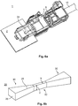
- Figure 6a shows a perspective exploded depiction of a plug connection arrangement 1 according to a fourth exemplary embodiment.
- the plug connection arrangement 1 has a connecting element 24.
- the connecting element 24 here serves as a coupling between the at least one radiation source 16 and the dielectric waveguide 10.
- the connecting element 24 is here positioned in the housing 4 between the radiation source 16 and an end of the dielectric waveguide 10.
- Various spacings between the radiation source 16 and the dielectric waveguide 10 can be bridged in the inserted state by the connecting element 24.
- the connecting element 24 serves as a metallic waveguide.
- Figure 6b represents a perspective depiction of the one-part connecting element 24 of the plug connection arrangement 1 according to the fourth exemplary embodiment.
- the connecting element 24 is formed straight and has a rectangular cross-section.
- the connecting element 24 here has an inner volume 26, which is permeable for electromagnetic radiation and made of a plastics material, and a metallised outer lateral surface 28.
- the connecting element 24 has, at its ends, in each case a region 30 with a cross-section which is conically expanded at the end.
- the connecting element 24 has, between the end regions with conically expanded cross-sections 30, a central region 32 for low-loss transmission of electromagnetic rays.
- the central region 32 has a greater height y than a half propagation wavelength of the electromagnetic radiation and a smaller width x than the height y. As a result of this, a so-called "single-mode" propagation of the electromagnetic radiation can be realised in the central region 32.
- Figure 7a shows a perspective depiction of a plug connection arrangement 1 according to a fifth exemplary embodiment.
- the dielectric waveguide 10 is spaced apart, at its end, from the printed circuit board 2 and thus has a height offset dy from a radiation source 16 arranged on the printed circuit board 2.
- the connecting element 24 is designed to be bent in the central region 32, such that the spacing between the radiation source 16 and the dielectric waveguide 10 can be bridged with low losses.
- the central region 32 is designed to be bent such that the electromagnetic radiation is perpendicularly and directly coupled into the connecting element 24 and subsequently can be perpendicularly coupled out of the connecting element 24 into the dielectric waveguide 10.
- the dielectric waveguide 10 can be received by the receiving unit 6 in a horizontal manner. Moreover, the dielectric waveguide 10 ends with the end-sleeve 12, as a result of which a production can be simplified and a durability of the dielectric waveguide 10 can be increased.
- Figure 7b separately depicts a perspective depiction of the one-part connecting element 24 of the plug connection arrangement 1 according to the fifth exemplary embodiment from Figure 7a .
- Figure 8a shows a perspective depiction of a plug connection arrangement 1 according to a sixth exemplary embodiment.
- the housing 4 has an intermediate space between the dielectric waveguide 10 and the radiation source 16.
- a two-part connecting element 24 is connected to the housing in a form-fitting manner.
- FIG 8b represents a perspective depiction of the multi-part connecting element 24 of the plug connection arrangement 1 according to the sixth exemplary embodiment from Figure 8a .
- the construction of the connecting element 24 is illustrated.
- Each half of the connecting element 24 has a cavity which defines the inner volume 26 of the connecting element 24.
- the cavity is coated with a metal and thus forms a metallic waveguide.
- the two parts of the connecting element 24 can be connected to one another in a form-fitting manner and can be inserted into the housing 4 together as a unit.
- the inner volume 26 is filled with air, according to the exemplary embodiment.
- FIG. 9 depicts a schematic depiction of a system 34 for transmitting data according to a first exemplary embodiment.
- the system 34 has a first controller 36 and a second controller 38.
- Each controller 36, 38 has one plug connection arrangement 1 each arranged in a controller housing 40.
- the plug connection arrangements 1 of the controllers 34, 36 are arranged such that they are each arranged on the rims of the printed circuit boards 2 and project out of the controller housings 40 at least in sections.
- the plug connection arrangements 1 do not have to be electromagnetically coupled into the controllers 36, 38 via further dielectric waveguides 10 and couplings.
- the two controllers 36, 38 are electromagnetically coupled to one another via an externally arranged dielectric waveguide 10 and can exchange information with one another with the help of the electromagnetic radiation.
Landscapes
- Physics & Mathematics (AREA)
- General Physics & Mathematics (AREA)
- Optics & Photonics (AREA)
- Waveguide Aerials (AREA)
- Waveguides (AREA)
- Radar Systems Or Details Thereof (AREA)
Abstract
having the at least one dielectric waveguide, wherein the at least one radiation source is enclosed, in a mounted state on the printed circuit board, at least in sections, by the housing and at least one receiving unit for receiving and aligning the at least one dielectric waveguide is connected to the housing, and wherein a dielectric waveguide, which can be received by the at least one receiving unit, in the received state, can be electromagnetically coupled to the at least one radiation source. Moreover, a system for transmitting data by electromagnetic radiation is disclosed.
Description
- The invention relates to a plug connection arrangement for mechanically and electromagnetically coupling at least one radiation source to at least one dielectric waveguide, having at least one housing which can be mounted on a printed circuit board, having the at least one radiation source for generating electromagnetic waves and having at least one dielectric waveguide. Moreover, the invention relates to a system for transmitting data by electromagnetic radiation between at least two controllers.
- Systems with high-frequency carrier signals can be used for future communication methods with high data transmission rates. Such high-frequency carrier signals are electromagnetic rays with a wavelength in the millimetre or micrometre range. However, radiation sources provided for this purpose have a limited available power in the frequency range limited for a data transmission. In order to be able to guarantee a data transmission, receiving units require a defined minimum signal strength.
- In particular in the automobile industry, transmission lengths for electromagnetic radiation of between 10 and 15 m are required. With dielectric waveguides, the electromagnetic rays can be guided over these transmission lengths. Due to the losses inside the dielectric waveguides and in the plug connections or couplings of the dielectric waveguides, guaranteeing the defined minimum signal strength can be problematic. The dielectric waveguides must thus have as low an attenuation as possible of the transmitted electromagnetic radiation. However, the dielectric waveguides can be established with regard to a material selection, length and arrangement. Moreover, optimisations of the actuators or the radiation sources and the dielectric waveguides are often only possible with great effort.
- The problem of the invention can be seen as proposing an improved plug connection arrangement with reduced electromagnetic losses for coupling at least one radiation source with at least one dielectric waveguide.
- This problem is solved by means of the respective subject-matter of the independent claims. Advantageous configurations of the invention form the subject-matter of respective dependent subclaims.
- According to an aspect of the invention, a plug connection arrangement for mechanically and electromagnetically coupling at least one radiation source to at least one dielectric waveguide is provided. The plug connection arrangement has at least one housing, which can be mounted on a printed circuit board, at least one radiation source for generating electromagnetic waves and at least one dielectric waveguide. According to the invention, the at least one radiation source is enclosed, at least in sections, by the housing in a mounted state on the printed circuit board, at least one receiving unit for receiving and aligning the at least one dielectric waveguide being connected to the housing. A dielectric waveguide, which can be received by the at least one receiving unit, in the received state, can be electromagnetically coupled to the at least one radiation source.
- The at least one receiving unit can be connected to the housing. In particular, the at least one receiving unit can be latched onto the housing or pushed into the housing. The housing can thus serve as a protection or a cover for the at least one radiation source and as a mechanical attachment of the receiving unit onto the printed circuit board. The at least one radiation source can have one or more antennas. In particular, the at least one radiation source can also be an array of antennas. The receiving unit can receive and align a dielectric waveguide. For this purpose, the receiving unit can have, for example, a receiving opening formed according to a cross-section of the dielectric waveguide. For example, the receiving unit can have a cylindrical opening. The dielectric waveguide can be introduced into the receiving unit up to a defined depth. For this purpose, the receiving unit can have limiting elements or latching lugs for cooperating with corresponding recesses arranged at the end of the dielectric waveguide. The at least one dielectric waveguide can also have end sleeves at the end. The end sleeves can be received by a receiving unit and thus used indirectly for positioning or aligning the dielectric waveguides. The receiving unit can be used for precisely aligning and positioning at least one dielectric waveguide. The at least one dielectric waveguide can be aligned and positioned by the receiving unit relative to the at least one radiation source. The at least one dielectric waveguide can preferably be aligned such that the at least one radiation source, without a spacing, can couple the electromagnetic radiation into the dielectric waveguide. The electromagnetic radiation can be, for example, a radio wave signal, a radar wave signal or the like. Moreover, the at least one dielectric waveguide can be aligned, at its ends, perpendicular to a main lobe of the at least one radiation source by the receiving unit, such that losses during a transition of the electromagnetic radiation into the dielectric waveguide can be minimised. The entire electromagnetic radiation emitted by the at least one radiation source can preferably be introduced, and thus coupled into, the at least one dielectric waveguide. As a result of this, a plug connection arrangement for dielectric waveguides can be realised with minimal coupling losses between a radiation source and a dielectric waveguide. In particular, the at least one dielectric waveguide can be optimally aligned with different radiation patterns of the at least one radiation source by the receiving unit.
- According to an embodiment, the housing can be mounted on an edge of the printed circuit board, the at least one radiation source being arranged in the housing or on the printed circuit board. By arranging the housing on an edge of the printed circuit board, a transmission length of the dielectric waveguide can be reduced and thus the transmission losses can also be minimised.
- According to a further embodiment, the at least one dielectric waveguide, which can be received by the at least one receiving unit, is aligned parallel to a planar elongation of the printed circuit board. The at least one radiation source can be a so-called "end-fire" antenna with a radiation characteristic which is directed parallel to the planar elongation of the printed circuit board. The at least one dielectric waveguide can be connected, with low losses, in radiation-conducting manner to the radiation source by a correspondingly aligned receiving unit arranged at the rim of the printed circuit board. A transmission length of the at least one dielectric waveguide can be reduced by arranging the plug connection in an edge region of the printed circuit board. The attenuation of the electromagnetic radiation in the waveguide is length-dependent and can thus also be reduced.
- According to a further embodiment, the at least one dielectric waveguide, which can be received by the at least one receiving unit, is aligned perpendicular to a planar elongation of the printed circuit board. In this case, preferably so-called "broadside" antennas with a main lobe directed perpendicular to the planar elongation of the printed circuit board can be used as radiation sources. For example, patch antennas or arrays of patch antennas can be used as radiation sources. By way of a combination of the housing and the receiving unit, the at least one dielectric waveguide can be aligned and positioned optimally adapted to a radiation pattern of the at least one radiation source. As a result of this, the electromagnetic radiation can be coupled into the at least one dielectric waveguide in an efficient and interference-free manner. The housing can preferably cover the at least one radiation source and the actuator of the radiation source at least in sections in the mounted state on the printed circuit board. This enables a mechanical protection of the at least one radiation source and the actuator of the at least one radiation source. In this case, the housing can also have an electromagnetically permeable barrier between the at least one dielectric waveguide and the at least one radiation source, since the electromagnetic radiation can also be coupled through a material of the housing into the at least one dielectric waveguide.
- According to a further embodiment, the at least one dielectric waveguide, which can be received by the at least one receiving unit, is aligned at an angle between 0° und 90° relative to a planar elongation of the printed circuit board. Depending on an arrangement of the at least one radiation source and on further edge conditions and geometric conditions, it can be advantageous to be able to couple at least one dielectric waveguide at an angle with at least one radiation source. For this purpose, the at least one radiation source can have a main lobe incline which is adapted according to the alignment of the dielectric waveguide. The radiation source can be a "tilted slot" antenna, such as a Vivaldi antenna, or a "tapered slot" antenna with a reflector.
- According to a further embodiment, the at least one dielectric waveguide, which can be received by the at least one receiving unit, in the housing extends beyond the at least one receiving unit up to the at least one radiation source. As a result of this, a spacing between the at least one radiation source, arranged on the printed circuit board, and a receiving unit, arranged spaced apart from the printed circuit board, can be minimised. In this case, the spacing can be selected depending on a radiation pattern of the at least one radiation source. As a result of this, the losses when coupling the electromagnetic radiation generated by the at least one radiation source into the at least one dielectric waveguide can be minimised.
- According to a further embodiment, at least one connecting element is arranged between the at least one radiation source and the at least one dielectric waveguide to electromagnetically couple the at least one radiation source to the at least one dielectric waveguide. The connecting element can be used as an interconnection between the at least one radiation source and the at least one dielectric waveguide. As a result of this, an electromagnetic coupling between the at least one radiation source and the at least one dielectric waveguide can be improved and possible losses can be reduced. In particular, the electromagnetic coupling can be optimised if the at least one dielectric waveguide cannot be optimally aligned relative to the at least one radiation source or has an excessively large spacing from the at least one radiation source. The plug connection arrangement can be adaptable to various printed circuit board layouts in a flexible manner by way of the connecting element.
- According to a further embodiment, the connecting element is formed to be tubular and has a wall made of metal or made of a metal coating. In this case, the connecting element can, for example, consist of a metal or be formed in the form of a metal-coated bore in a carrier object. In this case, a side facing the at least one radiation source and a side facing the at least one dielectric waveguide remain without metallic coatings, for optimal conduction of the electromagnetic radiation. Alternatively, the connecting element can consist of a material which can transmit the electromagnetic radiation of the radiation source and can be metallically coated on the circumference. By way of the metallic coating, the connecting element can guide the electromagnetic radiation with low losses.
- According to a further embodiment, the connecting element has a rectangular cross-section and an air-filled or plastics-filled inner volume. The connecting element can, for example, consist of a polymer, such as PE, PTEE, PFA, PP or the like, and be provided with a metallic coating. Alternatively, the connecting element can be configured in the form of a bore metallised on the inside or in the form of a metal tube or metal profile. As a result, the connecting element can be technically simple to produce, with a subsequent adaptation, such as by applying heat and pressure, to different spaces between the radiation source and the dielectric waveguide being possible.
- According to a further embodiment, the connecting element, at its ends, respectively has a region with a conically widened cross-section. As a result of this, dependent on a radiation pattern and an elongation of the at least one radiation source, a maximal radiation power can be coupled into the connecting element. Similarly hereto, the coupling of the electromagnetic radiation into the at least one dielectric waveguide can be optimised by a corresponding enlarging of the cross-section of the connecting element in a transition region to the at least one dielectric waveguide. In particular in the transition region, the connecting element can be aligned perpendicular to an end surface of the dielectric waveguide, such that reflections at interfaces and thus also transition losses can be minimised.
- According to a further embodiment, the connecting element has a central region between the end regions, a rectangular cross-section of the central region having a greater height than a half propagation wavelength of the electromagnetic radiation and a smaller width than the height. The connecting element can be divided into three parts. The region directed towards the radiation source is increased in height and in width and thus also in cross-section in order to improve coupling-in. The dimensions are preferably dependent on the kind of the at least one radiation source and the carrier frequency of the electromagnetic radiation. The central region preferably has a constant rectangular cross-section for guiding the electromagnetic radiation. The central region preferably has such a height and width that a single-mode propagation of the electromagnetic radiation and as a result a transmission with as low a loss as possible of the electromagnetic radiation can be performed. The cross-section of third region of the connecting element is also increased. The third region is here adapted to the material of the dielectric waveguide and to the carrier frequency of the electromagnetic radiation. The cross-sections of the first and the third region are preferably conically widened at the ends.
- According to a further embodiment, the connecting element is designed to be straight or bent. In particular, the central region can be adapted such that, for example, height differences can be compensated by a bent shape. The at least one dielectric waveguide can be arranged in the receiving unit, spaced apart from the printed circuit board, and the at least one radiation source can be formed on the printed circuit board.
- According to a further embodiment, the connecting element is designed in one part or in multiple parts and can be inserted into the housing in a form-fitting or firmly-bonded manner. Alternatively to a connecting element designed in one part, the connecting element can also be formed in multiple parts. In particular, the connecting element can, for example, be assembled into an electromagnetically conductive channel, by way of two or more metallically coated shells. The electromagnetic radiation is weakened or attenuated less by the air in the conductive channel than by a plastics material. The connecting element can preferably be designed in two parts, wherein, in each part, a metallically coated channel half can be configured as a groove.
- According to a further embodiment, an actuator of the at least one radiation source is arranged on the printed circuit board or in the housing. As a result of this, the actuator and/or the at least one radiation source can be protected from external environmental influences, such as dirt, dust or moisture. In particular, all or one part of the electronic components, such as the radiation source or actuator of the radiation source, can be encapsulated or moulded in the housing, since the generated electromagnetic rays can be transmitted in particular by a plastics material of the housing.
- According to a further aspect of the invention, a system for transmitting data by electromagnetic radiation between at least one first controller and at least one second controller is provided. According to the invention, each controller of the system has a controller housing with at least one plug connection arrangement according to one aspect of the invention. Moreover, the at least two controllers are electromagnetically connected to one another via at least one dielectric waveguide arranged outside the controller housing.
- By way of such an arrangement of the plug connection, a transmission length can be reduced through the dielectric waveguide. As a result of this, the transmission losses in the dielectric waveguide can be reduced. A combination of "end-fire" antennas with plug connections, arranged at edge regions of the controller housings, for receiving the dielectric waveguides enables an efficient and robust electromagnetic connection between a radiation source and the dielectric waveguide. By using receiving units, dielectric waveguides can be aligned and fixed optimally adapted to the radiation sources or radiation receivers. The system reduces a number of necessary electromagnetic couplings between an electromagnetic radiation source and a radiation receiver or between a transmitter and a receiver. It is thus possible to reduce transmission losses and guarantee a required minimum signal strength for a signal transmission in the case of constant or greater transmission lengths.
- Preferred exemplary embodiments of the invention are explained hereinafter in greater detail using greatly simplified schematic depictions. In the drawings
- Fig. 1a
- shows a perspective exploded depiction of a plug connection arrangement according to a first exemplary embodiment,
- Fig. 1b
- shows a plan view of a plug connection arrangement according to the first exemplary embodiment,
- Fig. 2
- shows sectional depictions of various arrangements of a signal source in a plug connection arrangement according to the first exemplary embodiment,
- Fig. 3
- shows a perspective depiction of a plug connection arrangement according to a second exemplary embodiment,
- Fig. 4
- shows sectional depictions of various arrangements of a signal source in a plug connection arrangement according to the second exemplary embodiment,
- Fig. 5
- shows a perspective depiction of a plug connection arrangement according to a third exemplary embodiment,
- Fig. 6a
- shows a perspective exploded depiction of a plug connection arrangement according to a fourth exemplary embodiment,
- Fig. 6b
- shows a perspective depiction of a one-part connecting element of the plug connection arrangement according to the fourth exemplary embodiment,
- Fig. 7a
- shows a perspective depiction of a plug connection arrangement according to a fifth exemplary embodiment,
- Fig. 7b
- shows a perspective depiction of a one-part connecting element of the plug connection arrangement according to the fifth exemplary embodiment,
- Fig. 8a
- shows a perspective depiction of a plug connection arrangement according to a sixth exemplary embodiment,
- Fig. 8b
- shows a perspective depiction of a multi-part connecting element of the plug connection arrangement according to the sixth exemplary embodiment,
- Fig. 9
- shows a schematic depiction of a system for transmitting data according to a first exemplary embodiment.
- In the figures, the same structural elements each have the same reference numbers.
-
Figure 1a shows a perspective exploded depiction of aplug connection arrangement 1 according to a first exemplary embodiment. Theplug connection arrangement 1 has ahousing 4 arranged on a printedcircuit board 2. Thehousing 4 is mounted on a rim of the printedcircuit board 2 and projects beyond the rim of the printedcircuit board 2. A receivingunit 6 can be inserted into thehousing 4 in a form-fitting manner. The receivingunit 6 can engage in a releasable manner in thehousing 4, according to the exemplary embodiment. The receivingunit 6 has acylindrical opening 8 for receiving, at its end, adielectric waveguide 10. In this case, thedielectric waveguide 10 has, at its end, asleeve 12 with acircumferential recess 14. Thewaveguide 10 can be received in an engageable manner by the receivingunit 6 at a defined insertion depth by means of therecess 14. In this case, the receivingunit 6, in a state arranged in thehousing 4, projects into thehousing 4 such that the insertedwaveguide 10 can be spaced apart at its ends with a minimal spacing from aradiation source 16 positioned in thehousing 4. Thewaveguide 10, at its ends, advantageously does not have a spacing from theradiation source 16. Thewaveguide 10 is aligned parallel to a planar elongation of the printedcircuit board 2 relative to theradiation source 16 by the receivingunit 6. -
Figure 1b depicts a plan view of aplug connection arrangement 1 according to the first exemplary embodiment fromFigure 1a . For reasons of clarity, thehousing 4 is not represented in the region of the printedcircuit board 2, such that anintegrated switching circuit 18 and aradiation source 16 arranged on theintegrated switching circuit 18 are visible. The receivingunit 6 and thewaveguide 10 received by the receivingunit 6 are arranged directly adjacent to theradiation source 16 in the inserted state. As a result of this, theradiation source 16 can couple the generated electromagnetic rays into thewaveguide 10. Thewaveguide 10 can be aligned precisely to theradiation source 16 by the receivingunit 6. According to the exemplary embodiment, theradiation source 16 is a so-called "end-fire" antenna. In particular, the radiation source can be a Vivaldi antenna, a Yagi antenna, a horn antenna or a so-called "tapered substrate integrated waveguide" antenna. The integrated switching circuit asactuator 18 of theradiation source 16 and theradiation source 16 are in this case arranged in thehousing 4 and are connected in an electrically conductive manner to the printedcircuit board 2 by a surface mounting of thehousing 4. The arrow here illustrates a main radiation direction of theradiation source 16 or a direction of the main lobe of theradiation source 16. -
Figure 2 represents sectional depictions of various arrangements of asignal source 16 in aplug connection arrangement 1 according to the first exemplary embodiment. Some exemplary possibilities for arranging thesignal source 16 and theactuator 18 of thesignal source 16, and thewaveguide 10 aligned corresponding to thesignal source 16 are depicted. In this case, theactuator 18 can also be arranged outside of thehousing 4. Thesignal source 16 can, for example, be arranged on theactuator 18 or anintegrated circuit 18 of the actuator. In particular, thesignal source 16 can also be integrated into theintegrated circuit 18. As a further alternative, the at least oneradiation source 16 can be imprinted onto the printedcircuit board 2 or be formed on the printedcircuit board 2 by removing material. Theactuator 18 can be connected via one ormultiple bond wires 20, for example. According to a further alternative, anactuator 18 can be applied onto at least oneradiation source 16 arranged on the printedcircuit board 2. In this case, theactuator 18 or anintegrated circuit 18 can, for example, be soldered to the at least oneradiation source 16 by a ball grid array. The various possibilities for arranging the at least oneradiation source 16 and theactuator 18 can be realised depending on requirements for a necessary bandwidth and frequency of the electromagnetic radiation. -
Figure 3 shows a perspective depiction of aplug connection arrangement 1 according to a second exemplary embodiment. Theactuator 18 of theradiation source 16 is positioned on the printedcircuit board 2, in the form of anintegrated circuit 18, by surface-mounting. Theradiation source 16 is integrated in theactuator 18. According to the exemplary embodiment, theradiation source 16 is a so-called "broadside" antenna which has a directivity which is orthogonal to its planar elongation. Theradiation source 16 can be a patch antenna or an array of patch antennas, for example. Thehousing 4 is positioned over theradiation source 16, in order to enclose and cover theradiation source 16, at least in sections. The housing is mechanically connected to the printedcircuit board 2 and serves as a positioning aid and form-fitting receptacle for the receivingunit 6. In this case, the receivingunit 6 can be plugged and engaged vertically onto thehousing 4. The receivingunit 6 has a vertically configuredopening 8 for receiving and positioning thedielectric waveguide 10. Thewaveguide 10 is here aligned perpendicular to the planar elongation of the printedcircuit board 2 by the receivingunit 6. In the aligned state, thedielectric waveguide 10 is electromagnetically coupled to theradiation source 16 and can receive and guide the generated electromagnetic radiation. The arrow illustrates the radiation direction of theradiation source 16. -
Figure 4 shows sectional depictions of various arrangements of asignal source 16 in aplug connection arrangement 1 according to the second exemplary embodiment. In contrast to the arrangement possibilities shown inFigure 2 , according to the second exemplary embodiment, radiation sources are arranged with a radiation direction perpendicular to the planar elongation of the printedcircuit board 2. -
Figure 5 depicts a perspective depiction of aplug connection arrangement 1 according to a third exemplary embodiment. In contrast to the described exemplary embodiments, the plug connection arrangement has aradiation source 16 with a radiation direction tilted at an angle of 45° relative to the printedcircuit board 2. The arrow illustrates the propagation direction of a main lobe of the radiation source. The at least oneradiation source 16 can be, for example, an "endfire" antenna with a subsequent reflector, a subsequent lens or a subsequent conductor. Moreover, the at least oneradiation source 16 can be a phased-array antenna made of patch antennas or dipole antennas. The receivingunit 6 is arranged in thehousing 4 and can receive thedielectric waveguide 10 in an aligned manner corresponding to the radiation direction of the at least oneradiation source 16. In this case, thedielectric waveguide 10 is positioned by the receivingunit 6 in an aligned manner at an angle of 45° relative to the main beam of the at least oneradiation source 16. In order for the spacing between the at least oneradiation source 16 and thedielectric waveguide 10 to be minimal, thedielectric waveguide 10 does not end with the end-sleeve 12, but instead projects into thehousing 4 via the end-sleeve 12 with an extension section 22 up to theradiation source 16. -
Figure 6a shows a perspective exploded depiction of aplug connection arrangement 1 according to a fourth exemplary embodiment. In contrast to theplug connection arrangement 1 according to the first exemplary embodiment, theplug connection arrangement 1, according to the fourth exemplary embodiment, has a connectingelement 24. The connectingelement 24 here serves as a coupling between the at least oneradiation source 16 and thedielectric waveguide 10. The connectingelement 24 is here positioned in thehousing 4 between theradiation source 16 and an end of thedielectric waveguide 10. Various spacings between theradiation source 16 and thedielectric waveguide 10 can be bridged in the inserted state by the connectingelement 24. In this case, the connectingelement 24 serves as a metallic waveguide.Figure 6b represents a perspective depiction of the one-part connecting element 24 of theplug connection arrangement 1 according to the fourth exemplary embodiment. The connectingelement 24 is formed straight and has a rectangular cross-section. The connectingelement 24 here has aninner volume 26, which is permeable for electromagnetic radiation and made of a plastics material, and a metallised outerlateral surface 28. The connectingelement 24 has, at its ends, in each case aregion 30 with a cross-section which is conically expanded at the end. The connectingelement 24 has, between the end regions with conically expandedcross-sections 30, acentral region 32 for low-loss transmission of electromagnetic rays. Thecentral region 32 has a greater height y than a half propagation wavelength of the electromagnetic radiation and a smaller width x than the height y. As a result of this, a so-called "single-mode" propagation of the electromagnetic radiation can be realised in thecentral region 32. -
Figure 7a shows a perspective depiction of aplug connection arrangement 1 according to a fifth exemplary embodiment. In contrast to the fourth exemplary embodiment, thedielectric waveguide 10 is spaced apart, at its end, from the printedcircuit board 2 and thus has a height offset dy from aradiation source 16 arranged on the printedcircuit board 2. The connectingelement 24 is designed to be bent in thecentral region 32, such that the spacing between theradiation source 16 and thedielectric waveguide 10 can be bridged with low losses. In particular, thecentral region 32 is designed to be bent such that the electromagnetic radiation is perpendicularly and directly coupled into the connectingelement 24 and subsequently can be perpendicularly coupled out of the connectingelement 24 into thedielectric waveguide 10. As a result of this, thedielectric waveguide 10 can be received by the receivingunit 6 in a horizontal manner. Moreover, thedielectric waveguide 10 ends with the end-sleeve 12, as a result of which a production can be simplified and a durability of thedielectric waveguide 10 can be increased. -
Figure 7b separately depicts a perspective depiction of the one-part connecting element 24 of theplug connection arrangement 1 according to the fifth exemplary embodiment fromFigure 7a . -
Figure 8a shows a perspective depiction of aplug connection arrangement 1 according to a sixth exemplary embodiment. In contrast to the preceding exemplary embodiments of theplug connection arrangement 1, thehousing 4 has an intermediate space between thedielectric waveguide 10 and theradiation source 16. In the intermediate space, a two-part connecting element 24 is connected to the housing in a form-fitting manner. Here, the two-part connecting element 24, similarly to a one-part connecting element 24, electromagnetically couples theradiation source 16 to thedielectric waveguide 10. -
Figure 8b represents a perspective depiction of the multi-part connectingelement 24 of theplug connection arrangement 1 according to the sixth exemplary embodiment fromFigure 8a . The construction of the connectingelement 24 is illustrated. Each half of the connectingelement 24 has a cavity which defines theinner volume 26 of the connectingelement 24. In this case, the cavity is coated with a metal and thus forms a metallic waveguide. The two parts of the connectingelement 24 can be connected to one another in a form-fitting manner and can be inserted into thehousing 4 together as a unit. Theinner volume 26 is filled with air, according to the exemplary embodiment. -
Figure 9 depicts a schematic depiction of asystem 34 for transmitting data according to a first exemplary embodiment. Thesystem 34 has afirst controller 36 and asecond controller 38. Eachcontroller plug connection arrangement 1 each arranged in acontroller housing 40. In this case, theplug connection arrangements 1 of thecontrollers circuit boards 2 and project out of thecontroller housings 40 at least in sections. As a result of this, theplug connection arrangements 1 do not have to be electromagnetically coupled into thecontrollers dielectric waveguides 10 and couplings. The twocontrollers dielectric waveguide 10 and can exchange information with one another with the help of the electromagnetic radiation. -
- 1
- Plug connection arrangement
- 2
- Printed circuit board
- 4
- Housing
- 6
- Receiving unit
- 8
- Cylindrical opening of the receiving unit
- 10
- Dielectric waveguide
- 12
- End-sleeve
- 14
- Circumferential recess
- 16
- At least one radiation source
- 18
- Actuator of the radiation source
- 20
- Bond wire
- 22
- Extension section of the waveguide
- 24
- Connecting element
- 26
- Inner volume
- 28
- Metallised lateral surface
- 30
- End region of the connecting element
- 32
- Central region
- 34
- System
- 36
- First controller
- 38
- Second controller
- 40
- Controller housing
- x
- Width of the central region
- y
- Height of the central region
- dy
- Height offset
Claims (15)
- A plug connection arrangement (1) for mechanically and electromagnetically coupling at least one radiation source (16) to at least one dielectric waveguide (10),having at least one housing (4) which can be mounted on a printed circuit board (2),having the at least one radiation source (16) for generating electromagnetic waves andhaving the at least one dielectric waveguide (10), characterised in thatthe at least one radiation source (16) is enclosed, at least in sections, by the housing (4) in a mounted state on the printed circuit board (2), whereinat least one receiving unit (6) for receiving and aligning the at least one dielectric waveguide (10) is connected to the housing (4) andwherein a dielectric waveguide (10), which can be received by the at least one receiving unit (6), in the received state, can be electromagnetically coupled to the at least one radiation source (16), directly or through a material of the housing (4).
- The plug connection arrangement according to Claim 1, wherein the housing (4) can be mounted on an edge of the printed circuit board (2), and wherein the at least one radiation source (16) is arranged in the housing (4) and/or on the printed circuit board (2).
- The plug connection arrangement according to Claim 1 or 2, wherein the at least one dielectric waveguide (10), which can be received by the at least one receiving unit (6), is aligned parallel to a planar elongation of the printed circuit board (2).
- The plug connection arrangement according to any one of Claims 1 to 3, wherein the at least one dielectric waveguide (10), which can be received by the at least one receiving unit (6), is aligned perpendicular to a planar elongation of the printed circuit board (2).
- The plug connection arrangement according to any one of Claims 1 to 4, wherein the at least one dielectric waveguide (10), which can be received by the at least one receiving unit (6), is aligned at an angle between 0° and 90° relative to a planar elongation of the printed circuit board (2).
- The plug connection arrangement according to Claim 5, wherein the at least one dielectric waveguide (10), which can be received by the at least one receiving unit (6), in the housing (4) extends beyond the at least one receiving unit (6) up to the at least one radiation source (16).
- The plug connection arrangement according to any one of Claims 1 to 5, wherein at least one connecting element (24) is arranged between the at least one radiation source (16) and the at least one dielectric waveguide (10) to electromagnetically couple the at least one radiation source (16) to the at least one dielectric waveguide (10).
- The plug connection arrangement according to Claim 7, wherein the connecting element (24) is formed to be tubular, has an air-filled or plastics-filled inner volume and has a wall (28) made of metal or made of a metal coating.
- The plug connection arrangement according to Claim 7 or 8, wherein the connecting element (24) has a rectangular cross-section and has an air-filled or plastics-filled inner volume (26) .
- The plug connection arrangement according to any one of Claims 7 to 9, wherein the connecting element (24) has, at each end, a region (30) with a conically expanded cross-section.
- The plug connection arrangement according to any one of Claims 7 to 10, wherein the connecting element (24) has a central region (32) between the end regions (30), wherein a rectangular cross-section of the central region (32) has at least a height (y) of a half propagation wavelength of the electromagnetic radiation and a smaller width (x) than the height (y).
- The plug connection arrangement according to any one of Claims 7 to 11, wherein the connecting element (24) is designed to be straight or bent.
- The plug connection arrangement according to any one of Claims 7 to 12, wherein the connecting element (24) is designed in one part or in multiple parts and can be inserted into the housing (4) in a form-fitting or firmly-bonded manner.
- The plug connection arrangement according to any one of Claims 1 to 13, wherein an actuator (18) of the at least one radiation source (16) is arranged on the printed circuit board (2) or in the housing (4).
- A system (34) for transmitting data by electromagnetic radiation between at least one first controller (36) and at least one second controller (38), wherein each controller (36, 38) has a controller housing (40) with at least one plug connection arrangement (1) according to any one of Claims 1 to 14 and are electromagnetically connected to one another via at least one dielectric waveguide (10) which is arranged outside the controller housing (40).
Applications Claiming Priority (1)
| Application Number | Priority Date | Filing Date | Title |
|---|---|---|---|
| DE102017122600.1A DE102017122600A1 (en) | 2017-09-28 | 2017-09-28 | Low-loss connector assembly and system with at least one such connector assembly |
Publications (2)
| Publication Number | Publication Date |
|---|---|
| EP3462533A1 true EP3462533A1 (en) | 2019-04-03 |
| EP3462533B1 EP3462533B1 (en) | 2023-08-09 |
Family
ID=63762206
Family Applications (1)
| Application Number | Title | Priority Date | Filing Date |
|---|---|---|---|
| EP18196896.7A Active EP3462533B1 (en) | 2017-09-28 | 2018-09-26 | Low-loss plug connection arrangement and system having at least one such plug connection arrangement |
Country Status (6)
| Country | Link |
|---|---|
| US (1) | US10938081B2 (en) |
| EP (1) | EP3462533B1 (en) |
| JP (1) | JP7281262B2 (en) |
| KR (1) | KR102652776B1 (en) |
| CN (1) | CN109586027B (en) |
| DE (1) | DE102017122600A1 (en) |
Cited By (1)
| Publication number | Priority date | Publication date | Assignee | Title |
|---|---|---|---|---|
| EP3787100A1 (en) * | 2019-08-30 | 2021-03-03 | TE Connectivity Germany GmbH | Redirecting device for mm-waves, connection assembly |
Families Citing this family (11)
| Publication number | Priority date | Publication date | Assignee | Title |
|---|---|---|---|---|
| KR102230313B1 (en) * | 2018-04-06 | 2021-03-22 | 한국과학기술원 | Connector for connecting waveguide and board |
| DE102018132285A1 (en) | 2018-12-14 | 2020-06-18 | Endress+Hauser SE+Co. KG | Level meter |
| WO2020202634A1 (en) | 2019-03-29 | 2020-10-08 | 富士フイルム株式会社 | Microcapsules, microcapsule composition, ink composition, coating material, and resin composition |
| CN114450849B (en) * | 2019-05-14 | 2024-08-27 | 申泰公司 | Wireless RF Waveguide Cable Assemblies |
| DE102020112787A1 (en) | 2020-01-13 | 2021-07-29 | Infineon Technologies Ag | High frequency device with high frequency chip and waveguide structure |
| US12464636B2 (en) | 2020-06-03 | 2025-11-04 | Huber+Suhner Ag | Polymer microwave fiber transceiver |
| EP4044362B1 (en) * | 2021-02-11 | 2026-04-01 | Aptiv Technologies AG | Connector for plastic wave guide and interconnect assembly comprising the connector |
| EP4063805B1 (en) * | 2021-03-22 | 2025-03-12 | Rosemount Tank Radar AB | Microwave transmission arrangement with encapsulation, communication and/or measurement system and radar level gauge system |
| CN113611990B (en) * | 2021-06-21 | 2022-09-23 | 北京无线电测量研究所 | PIN tube microwave switch module |
| EP4415157A1 (en) * | 2023-02-09 | 2024-08-14 | Universidad Carlos III de Madrid | External port |
| WO2025259710A1 (en) * | 2024-06-10 | 2025-12-18 | Redpoint Microwave, LLC | Radio frequency probes |
Citations (4)
| Publication number | Priority date | Publication date | Assignee | Title |
|---|---|---|---|---|
| US5600289A (en) * | 1994-08-30 | 1997-02-04 | Murata Manufacturing Co., Ltd. | Measuring jig used for evaluation of a device with a nonradiative dielectric waveguide |
| US20120153969A1 (en) * | 2010-12-15 | 2012-06-21 | Endress + Hauser Gmbh + Co. Kg | Measuring device working with microwave |
| FR3022696A1 (en) * | 2014-06-24 | 2015-12-25 | St Microelectronics Sa | CONNECTOR FOR PLASTIC WAVEGUIDE |
| US9490518B1 (en) * | 2015-09-28 | 2016-11-08 | Texas Instruments Incorporated | System for launching a signal into a dielectric waveguide |
Family Cites Families (17)
| Publication number | Priority date | Publication date | Assignee | Title |
|---|---|---|---|---|
| JPH0982420A (en) * | 1995-09-12 | 1997-03-28 | Hitachi Ltd | connector |
| EP1671401B1 (en) * | 2003-09-17 | 2019-05-22 | Huber+Suhner Ag | Coaxial plug-and-socket connector |
| JP2007006198A (en) | 2005-06-24 | 2007-01-11 | Hitachi Kokusai Electric Inc | High frequency circuit equipment |
| DE102008060430B4 (en) * | 2008-12-04 | 2010-09-30 | Tyco Electronics Amp Gmbh | Connector housing with light guide |
| CN102044733A (en) | 2009-10-23 | 2011-05-04 | 西安金波科技有限责任公司 | Coaxial millimeter wave adaptor with air-tight waveguide |
| JP5375738B2 (en) * | 2010-05-18 | 2013-12-25 | ソニー株式会社 | Signal transmission system |
| CN102544813A (en) * | 2010-12-30 | 2012-07-04 | 富士康(昆山)电脑接插件有限公司 | Photoelectric composite electric connector |
| JP5522088B2 (en) * | 2011-03-02 | 2014-06-18 | 日立金属株式会社 | Photoelectric transmission module |
| JP2014007456A (en) | 2012-06-21 | 2014-01-16 | Furuno Electric Co Ltd | Coaxial waveguide converter and manufacturing method therefor |
| US9306259B2 (en) | 2013-03-19 | 2016-04-05 | Texas Instruments Incorporated | Horn antenna for launching electromagnetic signal from microstrip to dielectric waveguide |
| JP6104672B2 (en) | 2013-03-29 | 2017-03-29 | モレックス エルエルシー | High frequency transmission equipment |
| WO2014171292A1 (en) | 2013-04-18 | 2014-10-23 | ソニー株式会社 | Connector device and wireless transmission system |
| TWI552430B (en) | 2013-09-26 | 2016-10-01 | 財團法人工業技術研究院 | Connector, antenna and electronic device |
| JP6417329B2 (en) | 2013-10-01 | 2018-11-07 | ソニーセミコンダクタソリューションズ株式会社 | Connector device and communication system |
| EP2876747B1 (en) * | 2013-11-21 | 2018-04-25 | Spinner GmbH | RF connector assembly |
| DE102015105657B4 (en) * | 2015-04-14 | 2018-12-06 | Infineon Technologies Ag | Dielectric waveguide connector |
| WO2017033668A1 (en) * | 2015-08-26 | 2017-03-02 | ソニーセミコンダクタソリューションズ株式会社 | Connector device and communication device |
-
2017
- 2017-09-28 DE DE102017122600.1A patent/DE102017122600A1/en not_active Ceased
-
2018
- 2018-09-26 JP JP2018179581A patent/JP7281262B2/en active Active
- 2018-09-26 EP EP18196896.7A patent/EP3462533B1/en active Active
- 2018-09-27 US US16/144,281 patent/US10938081B2/en active Active
- 2018-09-27 KR KR1020180115297A patent/KR102652776B1/en active Active
- 2018-09-28 CN CN201811137978.7A patent/CN109586027B/en active Active
Patent Citations (4)
| Publication number | Priority date | Publication date | Assignee | Title |
|---|---|---|---|---|
| US5600289A (en) * | 1994-08-30 | 1997-02-04 | Murata Manufacturing Co., Ltd. | Measuring jig used for evaluation of a device with a nonradiative dielectric waveguide |
| US20120153969A1 (en) * | 2010-12-15 | 2012-06-21 | Endress + Hauser Gmbh + Co. Kg | Measuring device working with microwave |
| FR3022696A1 (en) * | 2014-06-24 | 2015-12-25 | St Microelectronics Sa | CONNECTOR FOR PLASTIC WAVEGUIDE |
| US9490518B1 (en) * | 2015-09-28 | 2016-11-08 | Texas Instruments Incorporated | System for launching a signal into a dielectric waveguide |
Cited By (2)
| Publication number | Priority date | Publication date | Assignee | Title |
|---|---|---|---|---|
| EP3787100A1 (en) * | 2019-08-30 | 2021-03-03 | TE Connectivity Germany GmbH | Redirecting device for mm-waves, connection assembly |
| US11664562B2 (en) | 2019-08-30 | 2023-05-30 | Te Connectivity Germany Gmbh | Redirecting device for mm-waves, connection assembly |
Also Published As
| Publication number | Publication date |
|---|---|
| KR102652776B1 (en) | 2024-03-28 |
| US20190097294A1 (en) | 2019-03-28 |
| DE102017122600A1 (en) | 2019-03-28 |
| KR20190037160A (en) | 2019-04-05 |
| JP7281262B2 (en) | 2023-05-25 |
| EP3462533B1 (en) | 2023-08-09 |
| CN109586027B (en) | 2022-09-02 |
| JP2019068415A (en) | 2019-04-25 |
| US10938081B2 (en) | 2021-03-02 |
| CN109586027A (en) | 2019-04-05 |
Similar Documents
| Publication | Publication Date | Title |
|---|---|---|
| EP3462533B1 (en) | Low-loss plug connection arrangement and system having at least one such plug connection arrangement | |
| EP1158604B1 (en) | Antenna, antenna device, and radio equipment | |
| US6271799B1 (en) | Antenna horn and associated methods | |
| CN101663795A (en) | Patch antenna with metallic wall | |
| CN110226267B (en) | Plug connector for connecting a waveguide to at least one electrical conductor | |
| CN111342249B (en) | Connector for coaxial cable | |
| JP2014075682A (en) | Substrate integrated antenna module | |
| US6603438B2 (en) | High power broadband feed | |
| JP2001326506A (en) | Array antenna | |
| US7180461B2 (en) | Wideband omnidirectional antenna | |
| KR100662733B1 (en) | Waveguide Slot Antenna | |
| CN120545705A (en) | Waveguide antenna, waveguide antenna array and radar antenna | |
| KR20080085362A (en) | Antenna and its formation method and mobile communication terminal using same | |
| EP1547191B1 (en) | Parallel plate waveguide structure | |
| KR102266625B1 (en) | Omni Directional Antenna Apparatus for Vehicle | |
| US7286086B2 (en) | Gain-adjustable antenna | |
| KR100801685B1 (en) | Waveguide slot antenna | |
| CN101682124A (en) | Tapered slot antenna | |
| US7176836B2 (en) | Antenna system designed to enhance power efficiency | |
| KR102854095B1 (en) | Communication line | |
| KR200324767Y1 (en) | The slot antenna for waveguide | |
| KR20120138447A (en) | Low loss transition with multi-bend waveguide | |
| JP4333328B2 (en) | Slot antenna with sealed reflector | |
| CN118369819A (en) | Waveguides for guiding radio frequency signals | |
| CN113314826A (en) | Antenna structure and wireless transmission device |
Legal Events
| Date | Code | Title | Description |
|---|---|---|---|
| PUAI | Public reference made under article 153(3) epc to a published international application that has entered the european phase |
Free format text: ORIGINAL CODE: 0009012 |
|
| STAA | Information on the status of an ep patent application or granted ep patent |
Free format text: STATUS: THE APPLICATION HAS BEEN PUBLISHED |
|
| AK | Designated contracting states |
Kind code of ref document: A1 Designated state(s): AL AT BE BG CH CY CZ DE DK EE ES FI FR GB GR HR HU IE IS IT LI LT LU LV MC MK MT NL NO PL PT RO RS SE SI SK SM TR |
|
| AX | Request for extension of the european patent |
Extension state: BA ME |
|
| STAA | Information on the status of an ep patent application or granted ep patent |
Free format text: STATUS: REQUEST FOR EXAMINATION WAS MADE |
|
| 17P | Request for examination filed |
Effective date: 20190925 |
|
| RBV | Designated contracting states (corrected) |
Designated state(s): AL AT BE BG CH CY CZ DE DK EE ES FI FR GB GR HR HU IE IS IT LI LT LU LV MC MK MT NL NO PL PT RO RS SE SI SK SM TR |
|
| STAA | Information on the status of an ep patent application or granted ep patent |
Free format text: STATUS: EXAMINATION IS IN PROGRESS |
|
| 17Q | First examination report despatched |
Effective date: 20200414 |
|
| GRAP | Despatch of communication of intention to grant a patent |
Free format text: ORIGINAL CODE: EPIDOSNIGR1 |
|
| STAA | Information on the status of an ep patent application or granted ep patent |
Free format text: STATUS: GRANT OF PATENT IS INTENDED |
|
| RIC1 | Information provided on ipc code assigned before grant |
Ipc: H05K 1/02 20060101ALN20230203BHEP Ipc: G02B 6/42 20060101ALN20230203BHEP Ipc: H01P 5/08 20060101AFI20230203BHEP |
|
| INTG | Intention to grant announced |
Effective date: 20230228 |
|
| GRAS | Grant fee paid |
Free format text: ORIGINAL CODE: EPIDOSNIGR3 |
|
| GRAA | (expected) grant |
Free format text: ORIGINAL CODE: 0009210 |
|
| STAA | Information on the status of an ep patent application or granted ep patent |
Free format text: STATUS: THE PATENT HAS BEEN GRANTED |
|
| AK | Designated contracting states |
Kind code of ref document: B1 Designated state(s): AL AT BE BG CH CY CZ DE DK EE ES FI FR GB GR HR HU IE IS IT LI LT LU LV MC MK MT NL NO PL PT RO RS SE SI SK SM TR |
|
| REG | Reference to a national code |
Ref country code: GB Ref legal event code: FG4D |
|
| REG | Reference to a national code |
Ref country code: CH Ref legal event code: EP |
|
| REG | Reference to a national code |
Ref country code: DE Ref legal event code: R096 Ref document number: 602018054908 Country of ref document: DE |
|
| REG | Reference to a national code |
Ref country code: IE Ref legal event code: FG4D |
|
| REG | Reference to a national code |
Ref country code: LT Ref legal event code: MG9D |
|
| REG | Reference to a national code |
Ref country code: NL Ref legal event code: MP Effective date: 20230809 |
|
| REG | Reference to a national code |
Ref country code: AT Ref legal event code: MK05 Ref document number: 1598592 Country of ref document: AT Kind code of ref document: T Effective date: 20230809 |
|
| PG25 | Lapsed in a contracting state [announced via postgrant information from national office to epo] |
Ref country code: GR Free format text: LAPSE BECAUSE OF FAILURE TO SUBMIT A TRANSLATION OF THE DESCRIPTION OR TO PAY THE FEE WITHIN THE PRESCRIBED TIME-LIMIT Effective date: 20231110 |
|
| PG25 | Lapsed in a contracting state [announced via postgrant information from national office to epo] |
Ref country code: IS Free format text: LAPSE BECAUSE OF FAILURE TO SUBMIT A TRANSLATION OF THE DESCRIPTION OR TO PAY THE FEE WITHIN THE PRESCRIBED TIME-LIMIT Effective date: 20231209 |
|
| PG25 | Lapsed in a contracting state [announced via postgrant information from national office to epo] |
Ref country code: SE Free format text: LAPSE BECAUSE OF FAILURE TO SUBMIT A TRANSLATION OF THE DESCRIPTION OR TO PAY THE FEE WITHIN THE PRESCRIBED TIME-LIMIT Effective date: 20230809 Ref country code: RS Free format text: LAPSE BECAUSE OF FAILURE TO SUBMIT A TRANSLATION OF THE DESCRIPTION OR TO PAY THE FEE WITHIN THE PRESCRIBED TIME-LIMIT Effective date: 20230809 Ref country code: PT Free format text: LAPSE BECAUSE OF FAILURE TO SUBMIT A TRANSLATION OF THE DESCRIPTION OR TO PAY THE FEE WITHIN THE PRESCRIBED TIME-LIMIT Effective date: 20231211 Ref country code: NO Free format text: LAPSE BECAUSE OF FAILURE TO SUBMIT A TRANSLATION OF THE DESCRIPTION OR TO PAY THE FEE WITHIN THE PRESCRIBED TIME-LIMIT Effective date: 20231109 Ref country code: NL Free format text: LAPSE BECAUSE OF FAILURE TO SUBMIT A TRANSLATION OF THE DESCRIPTION OR TO PAY THE FEE WITHIN THE PRESCRIBED TIME-LIMIT Effective date: 20230809 Ref country code: LV Free format text: LAPSE BECAUSE OF FAILURE TO SUBMIT A TRANSLATION OF THE DESCRIPTION OR TO PAY THE FEE WITHIN THE PRESCRIBED TIME-LIMIT Effective date: 20230809 Ref country code: LT Free format text: LAPSE BECAUSE OF FAILURE TO SUBMIT A TRANSLATION OF THE DESCRIPTION OR TO PAY THE FEE WITHIN THE PRESCRIBED TIME-LIMIT Effective date: 20230809 Ref country code: IS Free format text: LAPSE BECAUSE OF FAILURE TO SUBMIT A TRANSLATION OF THE DESCRIPTION OR TO PAY THE FEE WITHIN THE PRESCRIBED TIME-LIMIT Effective date: 20231209 Ref country code: HR Free format text: LAPSE BECAUSE OF FAILURE TO SUBMIT A TRANSLATION OF THE DESCRIPTION OR TO PAY THE FEE WITHIN THE PRESCRIBED TIME-LIMIT Effective date: 20230809 Ref country code: GR Free format text: LAPSE BECAUSE OF FAILURE TO SUBMIT A TRANSLATION OF THE DESCRIPTION OR TO PAY THE FEE WITHIN THE PRESCRIBED TIME-LIMIT Effective date: 20231110 Ref country code: FI Free format text: LAPSE BECAUSE OF FAILURE TO SUBMIT A TRANSLATION OF THE DESCRIPTION OR TO PAY THE FEE WITHIN THE PRESCRIBED TIME-LIMIT Effective date: 20230809 Ref country code: AT Free format text: LAPSE BECAUSE OF FAILURE TO SUBMIT A TRANSLATION OF THE DESCRIPTION OR TO PAY THE FEE WITHIN THE PRESCRIBED TIME-LIMIT Effective date: 20230809 |
|
| PG25 | Lapsed in a contracting state [announced via postgrant information from national office to epo] |
Ref country code: PL Free format text: LAPSE BECAUSE OF FAILURE TO SUBMIT A TRANSLATION OF THE DESCRIPTION OR TO PAY THE FEE WITHIN THE PRESCRIBED TIME-LIMIT Effective date: 20230809 |
|
| PG25 | Lapsed in a contracting state [announced via postgrant information from national office to epo] |
Ref country code: ES Free format text: LAPSE BECAUSE OF FAILURE TO SUBMIT A TRANSLATION OF THE DESCRIPTION OR TO PAY THE FEE WITHIN THE PRESCRIBED TIME-LIMIT Effective date: 20230809 |
|
| PG25 | Lapsed in a contracting state [announced via postgrant information from national office to epo] |
Ref country code: SM Free format text: LAPSE BECAUSE OF FAILURE TO SUBMIT A TRANSLATION OF THE DESCRIPTION OR TO PAY THE FEE WITHIN THE PRESCRIBED TIME-LIMIT Effective date: 20230809 Ref country code: RO Free format text: LAPSE BECAUSE OF FAILURE TO SUBMIT A TRANSLATION OF THE DESCRIPTION OR TO PAY THE FEE WITHIN THE PRESCRIBED TIME-LIMIT Effective date: 20230809 Ref country code: ES Free format text: LAPSE BECAUSE OF FAILURE TO SUBMIT A TRANSLATION OF THE DESCRIPTION OR TO PAY THE FEE WITHIN THE PRESCRIBED TIME-LIMIT Effective date: 20230809 Ref country code: EE Free format text: LAPSE BECAUSE OF FAILURE TO SUBMIT A TRANSLATION OF THE DESCRIPTION OR TO PAY THE FEE WITHIN THE PRESCRIBED TIME-LIMIT Effective date: 20230809 Ref country code: DK Free format text: LAPSE BECAUSE OF FAILURE TO SUBMIT A TRANSLATION OF THE DESCRIPTION OR TO PAY THE FEE WITHIN THE PRESCRIBED TIME-LIMIT Effective date: 20230809 Ref country code: CZ Free format text: LAPSE BECAUSE OF FAILURE TO SUBMIT A TRANSLATION OF THE DESCRIPTION OR TO PAY THE FEE WITHIN THE PRESCRIBED TIME-LIMIT Effective date: 20230809 Ref country code: SK Free format text: LAPSE BECAUSE OF FAILURE TO SUBMIT A TRANSLATION OF THE DESCRIPTION OR TO PAY THE FEE WITHIN THE PRESCRIBED TIME-LIMIT Effective date: 20230809 |
|
| REG | Reference to a national code |
Ref country code: CH Ref legal event code: PL |
|
| REG | Reference to a national code |
Ref country code: DE Ref legal event code: R097 Ref document number: 602018054908 Country of ref document: DE |
|
| PG25 | Lapsed in a contracting state [announced via postgrant information from national office to epo] |
Ref country code: LU Free format text: LAPSE BECAUSE OF NON-PAYMENT OF DUE FEES Effective date: 20230926 |
|
| REG | Reference to a national code |
Ref country code: BE Ref legal event code: MM Effective date: 20230930 |
|
| PG25 | Lapsed in a contracting state [announced via postgrant information from national office to epo] |
Ref country code: LU Free format text: LAPSE BECAUSE OF NON-PAYMENT OF DUE FEES Effective date: 20230926 Ref country code: IT Free format text: LAPSE BECAUSE OF FAILURE TO SUBMIT A TRANSLATION OF THE DESCRIPTION OR TO PAY THE FEE WITHIN THE PRESCRIBED TIME-LIMIT Effective date: 20230809 Ref country code: MC Free format text: LAPSE BECAUSE OF FAILURE TO SUBMIT A TRANSLATION OF THE DESCRIPTION OR TO PAY THE FEE WITHIN THE PRESCRIBED TIME-LIMIT Effective date: 20230809 |
|
| PLBE | No opposition filed within time limit |
Free format text: ORIGINAL CODE: 0009261 |
|
| STAA | Information on the status of an ep patent application or granted ep patent |
Free format text: STATUS: NO OPPOSITION FILED WITHIN TIME LIMIT |
|
| REG | Reference to a national code |
Ref country code: IE Ref legal event code: MM4A |
|
| PG25 | Lapsed in a contracting state [announced via postgrant information from national office to epo] |
Ref country code: IE Free format text: LAPSE BECAUSE OF NON-PAYMENT OF DUE FEES Effective date: 20230926 |
|
| 26N | No opposition filed |
Effective date: 20240513 |
|
| PG25 | Lapsed in a contracting state [announced via postgrant information from national office to epo] |
Ref country code: CH Free format text: LAPSE BECAUSE OF NON-PAYMENT OF DUE FEES Effective date: 20230930 |
|
| GBPC | Gb: european patent ceased through non-payment of renewal fee |
Effective date: 20231109 |
|
| PG25 | Lapsed in a contracting state [announced via postgrant information from national office to epo] |
Ref country code: IE Free format text: LAPSE BECAUSE OF NON-PAYMENT OF DUE FEES Effective date: 20230926 Ref country code: FR Free format text: LAPSE BECAUSE OF NON-PAYMENT OF DUE FEES Effective date: 20231009 Ref country code: CH Free format text: LAPSE BECAUSE OF NON-PAYMENT OF DUE FEES Effective date: 20230930 Ref country code: SI Free format text: LAPSE BECAUSE OF FAILURE TO SUBMIT A TRANSLATION OF THE DESCRIPTION OR TO PAY THE FEE WITHIN THE PRESCRIBED TIME-LIMIT Effective date: 20230809 |
|
| PG25 | Lapsed in a contracting state [announced via postgrant information from national office to epo] |
Ref country code: BE Free format text: LAPSE BECAUSE OF NON-PAYMENT OF DUE FEES Effective date: 20230930 |
|
| PG25 | Lapsed in a contracting state [announced via postgrant information from national office to epo] |
Ref country code: GB Free format text: LAPSE BECAUSE OF NON-PAYMENT OF DUE FEES Effective date: 20231109 |
|
| PG25 | Lapsed in a contracting state [announced via postgrant information from national office to epo] |
Ref country code: GB Free format text: LAPSE BECAUSE OF NON-PAYMENT OF DUE FEES Effective date: 20231109 |
|
| PG25 | Lapsed in a contracting state [announced via postgrant information from national office to epo] |
Ref country code: BG Free format text: LAPSE BECAUSE OF FAILURE TO SUBMIT A TRANSLATION OF THE DESCRIPTION OR TO PAY THE FEE WITHIN THE PRESCRIBED TIME-LIMIT Effective date: 20230809 |
|
| PG25 | Lapsed in a contracting state [announced via postgrant information from national office to epo] |
Ref country code: BG Free format text: LAPSE BECAUSE OF FAILURE TO SUBMIT A TRANSLATION OF THE DESCRIPTION OR TO PAY THE FEE WITHIN THE PRESCRIBED TIME-LIMIT Effective date: 20230809 |
|
| PG25 | Lapsed in a contracting state [announced via postgrant information from national office to epo] |
Ref country code: CY Free format text: LAPSE BECAUSE OF FAILURE TO SUBMIT A TRANSLATION OF THE DESCRIPTION OR TO PAY THE FEE WITHIN THE PRESCRIBED TIME-LIMIT; INVALID AB INITIO Effective date: 20180926 |
|
| PG25 | Lapsed in a contracting state [announced via postgrant information from national office to epo] |
Ref country code: HU Free format text: LAPSE BECAUSE OF FAILURE TO SUBMIT A TRANSLATION OF THE DESCRIPTION OR TO PAY THE FEE WITHIN THE PRESCRIBED TIME-LIMIT; INVALID AB INITIO Effective date: 20180926 |
|
| PGFP | Annual fee paid to national office [announced via postgrant information from national office to epo] |
Ref country code: DE Payment date: 20250702 Year of fee payment: 8 |
|
| PG25 | Lapsed in a contracting state [announced via postgrant information from national office to epo] |
Ref country code: TR Free format text: LAPSE BECAUSE OF FAILURE TO SUBMIT A TRANSLATION OF THE DESCRIPTION OR TO PAY THE FEE WITHIN THE PRESCRIBED TIME-LIMIT Effective date: 20230809 |