EP3462223A1 - Camera module and electronic apparatus - Google Patents
Camera module and electronic apparatus Download PDFInfo
- Publication number
- EP3462223A1 EP3462223A1 EP18197855.2A EP18197855A EP3462223A1 EP 3462223 A1 EP3462223 A1 EP 3462223A1 EP 18197855 A EP18197855 A EP 18197855A EP 3462223 A1 EP3462223 A1 EP 3462223A1
- Authority
- EP
- European Patent Office
- Prior art keywords
- lens group
- guide member
- camera module
- light guide
- electronic apparatus
- Prior art date
- Legal status (The legal status is an assumption and is not a legal conclusion. Google has not performed a legal analysis and makes no representation as to the accuracy of the status listed.)
- Granted
Links
Images
Classifications
-
- G—PHYSICS
- G03—PHOTOGRAPHY; CINEMATOGRAPHY; ANALOGOUS TECHNIQUES USING WAVES OTHER THAN OPTICAL WAVES; ELECTROGRAPHY; HOLOGRAPHY
- G03B—APPARATUS OR ARRANGEMENTS FOR TAKING PHOTOGRAPHS OR FOR PROJECTING OR VIEWING THEM; APPARATUS OR ARRANGEMENTS EMPLOYING ANALOGOUS TECHNIQUES USING WAVES OTHER THAN OPTICAL WAVES; ACCESSORIES THEREFOR
- G03B17/00—Details of cameras or camera bodies; Accessories therefor
- G03B17/02—Bodies
- G03B17/17—Bodies with reflectors arranged in beam forming the photographic image, e.g. for reducing dimensions of camera
-
- G—PHYSICS
- G02—OPTICS
- G02B—OPTICAL ELEMENTS, SYSTEMS OR APPARATUS
- G02B13/00—Optical objectives specially designed for the purposes specified below
- G02B13/001—Miniaturised objectives for electronic devices, e.g. portable telephones, webcams, PDAs, small digital cameras
- G02B13/0055—Miniaturised objectives for electronic devices, e.g. portable telephones, webcams, PDAs, small digital cameras employing a special optical element
- G02B13/0065—Miniaturised objectives for electronic devices, e.g. portable telephones, webcams, PDAs, small digital cameras employing a special optical element having a beam-folding prism or mirror
-
- G—PHYSICS
- G02—OPTICS
- G02B—OPTICAL ELEMENTS, SYSTEMS OR APPARATUS
- G02B13/00—Optical objectives specially designed for the purposes specified below
- G02B13/001—Miniaturised objectives for electronic devices, e.g. portable telephones, webcams, PDAs, small digital cameras
- G02B13/0055—Miniaturised objectives for electronic devices, e.g. portable telephones, webcams, PDAs, small digital cameras employing a special optical element
- G02B13/0065—Miniaturised objectives for electronic devices, e.g. portable telephones, webcams, PDAs, small digital cameras employing a special optical element having a beam-folding prism or mirror
- G02B13/007—Miniaturised objectives for electronic devices, e.g. portable telephones, webcams, PDAs, small digital cameras employing a special optical element having a beam-folding prism or mirror the beam folding prism having at least one curved surface
-
- G—PHYSICS
- G02—OPTICS
- G02B—OPTICAL ELEMENTS, SYSTEMS OR APPARATUS
- G02B13/00—Optical objectives specially designed for the purposes specified below
- G02B13/06—Panoramic objectives; So-called "sky lenses" including panoramic objectives having reflecting surfaces
-
- G—PHYSICS
- G02—OPTICS
- G02B—OPTICAL ELEMENTS, SYSTEMS OR APPARATUS
- G02B13/00—Optical objectives specially designed for the purposes specified below
- G02B13/16—Optical objectives specially designed for the purposes specified below for use in conjunction with image converters or intensifiers, or for use with projectors, e.g. objectives for projection TV
-
- G—PHYSICS
- G02—OPTICS
- G02B—OPTICAL ELEMENTS, SYSTEMS OR APPARATUS
- G02B17/00—Systems with reflecting surfaces, with or without refracting elements
- G02B17/08—Catadioptric systems
- G02B17/0856—Catadioptric systems comprising a refractive element with a reflective surface, the reflection taking place inside the element, e.g. Mangin mirrors
- G02B17/086—Catadioptric systems comprising a refractive element with a reflective surface, the reflection taking place inside the element, e.g. Mangin mirrors wherein the system is made of a single block of optical material, e.g. solid catadioptric systems
-
- G—PHYSICS
- G02—OPTICS
- G02B—OPTICAL ELEMENTS, SYSTEMS OR APPARATUS
- G02B5/00—Optical elements other than lenses
- G02B5/04—Prisms
Definitions
- the present disclosure relates to the field of terminal technologies, and in particular, to a camera module and an electronic apparatus.
- the built-in camera module may include a lens and an imaging device sequentially arranged in a thickness direction of the electronic apparatus.
- the lens may be used for collecting external light, and the external light after passing through the imaging device forms image information that the user may view on a display interface of the electronic apparatus.
- the present disclosure provides a camera module and an electronic apparatus for solving the deficiencies in the related art.
- a camera module including:
- the lens including: a lens group and a light guide member, and the light guide member including: a reflective surface and a curved incident surface formed by extending toward an outside of the light guide member; wherein the reflective surface is used for reflecting external light incident from the incident surface to the imaging device.
- the light guide member further includes: a curved exit surface formed to be recessed toward an inside of the light guide member, and the exit surface refracts the external light reflected by the reflective surface to the imaging device.
- the incident surface of the light guide member faces a light entrance of an electronic apparatus, and the external light reflected by the reflective surface faces the lens group.
- the lens group includes a first lens group and a second lens group, arrangement directions of the first lens group and the second lens group are perpendicular to each other, the incident surface of the light guide member faces the first lens group, and the external light reflected by the reflective surface faces the second lens group.
- the first lens group is assembled to a predetermined position along a thickness direction of an electronic apparatus, and the arrangement direction of the second lens group and the imaging device is perpendicular to the thickness direction of the electronic apparatus.
- the first lens group has a smaller size than the second lens group.
- the light guide member includes a prism.
- a reflective film is provided on the reflective surface of the light guide member.
- the external light is totally reflected on the reflective surface.
- an electronic apparatus which includes the camera module described in any one of the foregoing embodiments.
- the light guide member in the present disclosure can change a propagation path of the external light in the electronic apparatus and is conducive to the light and thin development of the electronic apparatus.
- the incident surface on the light guide member has a curved surface facing the incident light, thus a relatively wide perspective of visual field can be obtained, a shooting scene of the electronic apparatus can be expanded, and shooting needs of the user can be met.
- first information may also be referred to as second information.
- second information may also be referred to as first information.
- a term “if' as used herein can be interpreted as "when", “where” or "in response to”.
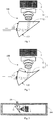
- Fig. 1 is a schematic structural diagram of a camera module according to an exemplary embodiment.
- the camera module 100 may include a lens 1 and an imaging device 2.
- the imaging device 2 may convert external light captured by the lens 1 into image information that a user can view on the electronic apparatus.
- the lens 1 may include a lens group 11 and a light guide member 12.
- the light guide member 12 may include a reflective surface 122 and a curved incident surface 121 formed by extending toward an outside of the light guide member 12. The external light incident from the incident surface 122 may be reflected into the imaging device 2 via the reflective surface 122.
- the incident surface 121 is provided in a curved shape (e.g., spherical shape or aspherical shape), a contact area between the external light and the incident surface 121 is increased, which can obtain a relatively wide angle of view for the camera module 100 and enlarge the shooting scene of the electronic apparatus.
- a curved shape e.g., spherical shape or aspherical shape
- the light guide member 12 may further include an exit surface 123.
- the exit surface 123 may be a curved surface that is concave toward the interior of the light guide member 12, so as to refract the external light reflected by the reflective surface 122 to the imaging device 2.
- the exit surface 123 which is recessed toward the interior of the light guide member 12, can refract the light from the reflective surface 122 to the imaging device 2 as much as possible, so as to increase the amount of light entering.
- the lens group 11 may include one or more lenses, and when the lens group 11 includes multiple pieces of lenses, the light convergence capability of the camera can be enhanced, and thus the imaging can be more close to the real. Also, depending on the number of lenses, there are a variety of situations in the arrangement of the light guide member 12 in the present disclosure.
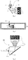
- the light guide member 12 may be closer to a light entrance 201 of the electronic apparatus 200 than the lens group 11.
- the incident surface 121 of the light guide member 12 may be disposed toward the light entrance 201 of the electronic apparatus 200, so that the external light refracted by the incident surface 121 may be reflected after entering the reflective surface 122, and the external light reflected by the reflective surface 122 faces the lens group 11.
- the light guide member 12 and the lens group 11 in the lens 1 may be respectively disposed in different directions of the electronic apparatus 200.
- the light guide member 12 may be disposed along the thickness direction of the electronic apparatus 200, and the lens group 11 and the imaging device 2 may be disposed in a horizontal direction of the electronic apparatus 200.
- the incident surface 121 is provided to be curved toward the light entrance 201, the physical size of the light entrance 201 can be reduced when the camera module 100 acquires equal amount of light, which is advantageous for improving a screen occupation ratio of the electronic apparatus 200.
- the lens group 11 may be closer to the light entrance 201 of the electronic apparatus 200 than the light guide member 12.
- the lens group 11 may include a first lens group 111 and a second lens group 112.
- the first lens group 111 may be disposed facing the light entrance 201.
- the external light incident through the first lens group 111 may be refracted by the incident surface 121 of the light guide member 12 onto the reflective surface 122, and the external light reflected by the reflective surface 122 may be directed toward the second lens group 112, so as to guide the external light into the imaging device 2 through the second lens group 112.
- the first lens group 111 and the second lens group 112 may be disposed in different directions of the electronic apparatus 200 because the reflective surface 122 may change the conduction path of the external light.
- the first lens group 111 may be disposed along the thickness direction of the electronic apparatus 200
- the second lens group 112 and the imaging device 2 may be disposed along the horizontal direction of the electronic apparatus 200, which is conducive to the thin and light development of the electronic apparatus 200.
- the size of the first lens group 111 may be smaller than the size of the second lens 112, so as to reduce a proportion of the lens 1 in the thickness direction of the electronic apparatus 200 and improve the screen occupation ratio of the electronic apparatus 200.
- the external light may be totally reflected on the reflective surface 122 of the light guide member 12 to minimize the loss of the external light and increase the amount of light entering.
- a reflective film 1221 may be disposed on the reflective surface 122 to increase the reflectivity.
- the reflective film 1221 may include a metal reflective film (e.g., an aluminum film, a silver film, etc.), a full dielectric reflective film, a metal dielectric reflective film combining the metal reflective film and full dielectric reflective film, or the like, which is not limited by the present disclosure.
- the light guide member 12 may include a prism, such as a triple prism, and the like, and further may be an isosceles right-angled triple prism, so that a total reflection may occur when the external light is refracted on a hypotenuse of the isosceles right-angled triple prism.
- the right-angled edges of the isosceles right-angled triple prism may be curved, so as to respectively serve as the incident surface and the exit surface of the light guide member 12, which increases the angle of view of the camera module 100 and meets the shooting needs of the user.
Landscapes
- Physics & Mathematics (AREA)
- General Physics & Mathematics (AREA)
- Optics & Photonics (AREA)
- Studio Devices (AREA)
- Structure And Mechanism Of Cameras (AREA)
- Optical Elements Other Than Lenses (AREA)
- Camera Bodies And Camera Details Or Accessories (AREA)
Abstract
Description
- The present disclosure relates to the field of terminal technologies, and in particular, to a camera module and an electronic apparatus.
- Currently, most electronic apparatuses have built-in camera modules to meet the needs of the user's daily photography. In general, the built-in camera module may include a lens and an imaging device sequentially arranged in a thickness direction of the electronic apparatus. The lens may be used for collecting external light, and the external light after passing through the imaging device forms image information that the user may view on a display interface of the electronic apparatus.
- The present disclosure provides a camera module and an electronic apparatus for solving the deficiencies in the related art.
- According to a first aspect of the embodiments of the present disclosure, there is provided a camera module, including:
- a lens and an imaging device, the lens including: a lens group and a light guide member, and the light guide member including: a reflective surface and a curved incident surface formed by extending toward an outside of the light guide member; wherein the reflective surface is used for reflecting external light incident from the incident surface to the imaging device.
- Optionally, the light guide member further includes: a curved exit surface formed to be recessed toward an inside of the light guide member, and the exit surface refracts the external light reflected by the reflective surface to the imaging device.
- Optionally, the incident surface of the light guide member faces a light entrance of an electronic apparatus, and the external light reflected by the reflective surface faces the lens group.
- Optionally, the lens group includes a first lens group and a second lens group, arrangement directions of the first lens group and the second lens group are perpendicular to each other, the incident surface of the light guide member faces the first lens group, and the external light reflected by the reflective surface faces the second lens group.
- Optionally, the first lens group is assembled to a predetermined position along a thickness direction of an electronic apparatus, and the arrangement direction of the second lens group and the imaging device is perpendicular to the thickness direction of the electronic apparatus.
- Optionally, the first lens group has a smaller size than the second lens group.
- Optionally, the light guide member includes a prism.
- Optionally, a reflective film is provided on the reflective surface of the light guide member.
- Optionally, the external light is totally reflected on the reflective surface.
- According to a second aspect of the embodiments of the present disclosure, an electronic apparatus is provided, which includes the camera module described in any one of the foregoing embodiments.
- It can be seen from the above embodiments that the light guide member in the present disclosure can change a propagation path of the external light in the electronic apparatus and is conducive to the light and thin development of the electronic apparatus. In addition, the incident surface on the light guide member has a curved surface facing the incident light, thus a relatively wide perspective of visual field can be obtained, a shooting scene of the electronic apparatus can be expanded, and shooting needs of the user can be met.
- It is to be understood that both the foregoing general description and the following detailed description are exemplary and explanatory only and are not restrictive of the invention, as claimed.
- The accompanying drawings, which are incorporated in and constitute a part of this specification, illustrate aspects consistent with the disclosure and, together with the description, serve to explain the principles of the disclosure.
-
Fig. 1 is a schematic structural diagram of a camera module according to an exemplary aspect of the present disclosure. -
Fig. 2 is a schematic structural diagram of another camera module according to an exemplary aspect of the present disclosure. -
Fig. 3 is an assembly diagram of a camera module and an electronic apparatus according to an exemplary aspect of the present disclosure. -
Fig. 4 is a schematic structural diagram of another camera module according to an exemplary aspect of the present disclosure. -
Fig. 5 is an assembly diagram of a camera module and an electronic apparatus according to an exemplary aspect of the present disclosure. -
Fig. 6 is a schematic structural diagram of another camera module according to an exemplary aspect of the present disclosure. - The specific aspects of the present disclosure, which have been illustrated by the accompanying drawings described above, will be described in detail below. These accompanying drawings and description are not intended to limit the scope of the present disclosure in any manner, but to explain the concept of the present disclosure to those skilled in the art via referencing specific aspects.
- Reference will now be made in detail to exemplary aspects, examples of which are illustrated in the accompanying drawings. The following description refers to the accompanying drawings in which the same numbers in different drawings represent the same or similar elements unless otherwise represented. The implementations set forth in the following description of exemplary aspects do not represent all implementations consistent with the present disclosure. Instead, they are merely examples of apparatuses and methods consistent with aspects related to the present disclosure as recited in the appended claims.
- The terms used herein are merely for describing a particular aspect, rather than limiting the present disclosure. As used in the present disclosure and the appended claims, terms in singular forms such as "a", "said" and "the" are intended to also include plural forms, unless explicitly dictated otherwise. It should also be understood that the term "and/or" used herein means any one or any possible combination of one or more associated listed items.
- It should be understood that, although it may describe information with a term first, second, or third, etc., the information is not limited by these terms. These terms are merely for distinguishing among information of the same kind. For example, without departing from the scope of the present disclosure, first information may also be referred to as second information. Similarly, second information may also be referred to as first information. Depending on the context, a term "if' as used herein can be interpreted as "when", "where" or "in response to".
-
Fig. 1 is a schematic structural diagram of a camera module according to an exemplary embodiment. As shown inFig. 1 , thecamera module 100 may include alens 1 and animaging device 2. Theimaging device 2 may convert external light captured by thelens 1 into image information that a user can view on the electronic apparatus. Thelens 1 may include alens group 11 and alight guide member 12. Thelight guide member 12 may include areflective surface 122 and acurved incident surface 121 formed by extending toward an outside of thelight guide member 12. The external light incident from theincident surface 122 may be reflected into theimaging device 2 via thereflective surface 122. Since theincident surface 121 is provided in a curved shape (e.g., spherical shape or aspherical shape), a contact area between the external light and theincident surface 121 is increased, which can obtain a relatively wide angle of view for thecamera module 100 and enlarge the shooting scene of the electronic apparatus. - Further, as shown in
Fig. 2 , thelight guide member 12 may further include anexit surface 123. Theexit surface 123 may be a curved surface that is concave toward the interior of thelight guide member 12, so as to refract the external light reflected by thereflective surface 122 to theimaging device 2. Theexit surface 123, which is recessed toward the interior of thelight guide member 12, can refract the light from thereflective surface 122 to theimaging device 2 as much as possible, so as to increase the amount of light entering. - In this aspect, the
lens group 11 may include one or more lenses, and when thelens group 11 includes multiple pieces of lenses, the light convergence capability of the camera can be enhanced, and thus the imaging can be more close to the real. Also, depending on the number of lenses, there are a variety of situations in the arrangement of thelight guide member 12 in the present disclosure. - In an aspect, as shown in
Fig. 3 , thelight guide member 12 may be closer to alight entrance 201 of theelectronic apparatus 200 than thelens group 11. For example, theincident surface 121 of thelight guide member 12 may be disposed toward thelight entrance 201 of theelectronic apparatus 200, so that the external light refracted by theincident surface 121 may be reflected after entering thereflective surface 122, and the external light reflected by thereflective surface 122 faces thelens group 11. - Because the
reflective surface 122 may change a transmission path of the external light, thelight guide member 12 and thelens group 11 in thelens 1 may be respectively disposed in different directions of theelectronic apparatus 200. For example, still taking the aspect shown inFig. 3 as an example, thelight guide member 12 may be disposed along the thickness direction of theelectronic apparatus 200, and thelens group 11 and theimaging device 2 may be disposed in a horizontal direction of theelectronic apparatus 200. In this way, by changing the arrangement direction of thecamera module 100, the development trend of lightness and thinness of theelectronic apparatus 200 is conformed to. In addition, since theincident surface 121 is provided to be curved toward thelight entrance 201, the physical size of thelight entrance 201 can be reduced when thecamera module 100 acquires equal amount of light, which is advantageous for improving a screen occupation ratio of theelectronic apparatus 200. - In another aspect, at least a portion of the
lens group 11 may be closer to thelight entrance 201 of theelectronic apparatus 200 than thelight guide member 12. For example, as shown inFig. 4 , thelens group 11 may include afirst lens group 111 and asecond lens group 112. As shown inFig. 5 , thefirst lens group 111 may be disposed facing thelight entrance 201. The external light incident through thefirst lens group 111 may be refracted by theincident surface 121 of thelight guide member 12 onto thereflective surface 122, and the external light reflected by thereflective surface 122 may be directed toward thesecond lens group 112, so as to guide the external light into theimaging device 2 through thesecond lens group 112. - Similarly, the
first lens group 111 and thesecond lens group 112 may be disposed in different directions of theelectronic apparatus 200 because thereflective surface 122 may change the conduction path of the external light. For example, still taking the aspect shown inFig. 5 as an example, thefirst lens group 111 may be disposed along the thickness direction of theelectronic apparatus 200, and thesecond lens group 112 and theimaging device 2 may be disposed along the horizontal direction of theelectronic apparatus 200, which is conducive to the thin and light development of theelectronic apparatus 200. Further, the size of thefirst lens group 111 may be smaller than the size of thesecond lens 112, so as to reduce a proportion of thelens 1 in the thickness direction of theelectronic apparatus 200 and improve the screen occupation ratio of theelectronic apparatus 200. - In each of the above aspects, the external light may be totally reflected on the
reflective surface 122 of thelight guide member 12 to minimize the loss of the external light and increase the amount of light entering. For example, as shown inFig. 6 , areflective film 1221 may be disposed on thereflective surface 122 to increase the reflectivity. Thereflective film 1221 may include a metal reflective film (e.g., an aluminum film, a silver film, etc.), a full dielectric reflective film, a metal dielectric reflective film combining the metal reflective film and full dielectric reflective film, or the like, which is not limited by the present disclosure. - Based on the technical solutions of the present disclosure, the
light guide member 12 may include a prism, such as a triple prism, and the like, and further may be an isosceles right-angled triple prism, so that a total reflection may occur when the external light is refracted on a hypotenuse of the isosceles right-angled triple prism. The right-angled edges of the isosceles right-angled triple prism may be curved, so as to respectively serve as the incident surface and the exit surface of thelight guide member 12, which increases the angle of view of thecamera module 100 and meets the shooting needs of the user.
Claims (10)
- A camera module, comprising:an imaging device (2); anda lens (1) including: a lens group (11) and a light guide member (12),
wherein the light guide member (12) includes: a reflective surface (122) and a curved incident surface (121) formed by extending toward an outside of the light guide member (12), and wherein the reflective surface (122) is used for reflecting external light incident from the incident surface (121) to the imaging device (2). - The camera module according to claim 1, wherein the light guide member (12) further includes: a curved exit surface formed to be recessed toward an inside of the light guide member (12), and the exit surface refracts the external light reflected by the reflective surface (122) to the imaging device (2).
- The camera module according to claim 1, wherein the incident surface of the light guide member (12) faces a light entrance (201) of an electronic apparatus, and the external light reflected by the reflective surface (122) faces the lens group (11).
- The camera module according to claim 1, wherein the lens group (11) includes a first lens group (111) and a second lens group (112), wherein arrangement directions of the first lens group (111) and the second lens group (112) are perpendicular to each other, the incident surface of the light guide member (12) faces the first lens group (111), and the external light reflected by the reflective surface (122) faces the second lens group (112).
- The camera module according to claim 4, wherein the first lens group (111) is assembled to a predetermined position along a thickness direction of an electronic apparatus, and the arrangement direction of the second lens group (112) and the imaging device (2) is perpendicular to the thickness direction of the electronic apparatus.
- The camera module according to claim 4, wherein the first lens group (111) has a smaller size than the second lens group (112).
- The camera module according to claim 1, wherein the light guide member (12) includes a prism.
- The camera module according to claim 1, wherein a reflection film is provided on the reflective surface (122) of the light guide member (12).
- The camera module according to claim 1, wherein the external light is totally reflected on the reflective surface (122).
- An electronic apparatus, including the camera module according to any one of claims 1-9.
Applications Claiming Priority (1)
| Application Number | Priority Date | Filing Date | Title |
|---|---|---|---|
| CN201710938101.7A CN109597186A (en) | 2017-09-30 | 2017-09-30 | Camera module and electronic equipment |
Publications (2)
| Publication Number | Publication Date |
|---|---|
| EP3462223A1 true EP3462223A1 (en) | 2019-04-03 |
| EP3462223B1 EP3462223B1 (en) | 2026-02-25 |
Family
ID=63720522
Family Applications (1)
| Application Number | Title | Priority Date | Filing Date |
|---|---|---|---|
| EP18197855.2A Active EP3462223B1 (en) | 2017-09-30 | 2018-10-01 | Electronic apparatus |
Country Status (3)
| Country | Link |
|---|---|
| US (1) | US11480852B2 (en) |
| EP (1) | EP3462223B1 (en) |
| CN (1) | CN109597186A (en) |
Families Citing this family (2)
| Publication number | Priority date | Publication date | Assignee | Title |
|---|---|---|---|---|
| CN110248006B (en) * | 2019-06-28 | 2021-04-23 | 武汉当代华路光电技术有限公司 | Mobile phone thin and light 3D camera |
| CN112188041A (en) * | 2019-07-03 | 2021-01-05 | 中兴通讯股份有限公司 | Camera module and electronic equipment |
Citations (3)
| Publication number | Priority date | Publication date | Assignee | Title |
|---|---|---|---|---|
| JP2004212737A (en) * | 2003-01-06 | 2004-07-29 | Nidec Copal Corp | Zoom lens |
| KR100683324B1 (en) * | 2004-10-21 | 2007-02-15 | 미쓰비시덴키 가부시키가이샤 | Zoom lens |
| WO2010011789A2 (en) * | 2008-07-22 | 2010-01-28 | Stereo Display, Inc. | Compact auto-focus image taking lens system with a micromirror array lens and a lens-surfaced prism |
Family Cites Families (13)
| Publication number | Priority date | Publication date | Assignee | Title |
|---|---|---|---|---|
| US6577454B2 (en) * | 2001-06-14 | 2003-06-10 | John M. Hall | Folded image intensifier objective lens |
| JP4869522B2 (en) | 2001-09-28 | 2012-02-08 | オリンパス株式会社 | Optical path bending zoom optical system |
| JP4450600B2 (en) * | 2003-03-10 | 2010-04-14 | 日本電産コパル株式会社 | Zoom lens |
| KR20100091435A (en) * | 2009-02-10 | 2010-08-19 | 삼성테크윈 주식회사 | Camera module and digital image processing apparatus therewith |
| CN102243349A (en) * | 2010-05-10 | 2011-11-16 | 鸿富锦精密工业(深圳)有限公司 | Refraction lens, lens module and imaging device with the lens module |
| JP2012068509A (en) * | 2010-09-24 | 2012-04-05 | Hoya Corp | Photographic optical system and photographic device |
| US9557627B2 (en) * | 2014-03-07 | 2017-01-31 | Apple Inc. | Folded camera lens systems |
| CN103955049A (en) * | 2014-05-21 | 2014-07-30 | 中山联合光电科技有限公司 | An optical fixed focus system |
| KR101792344B1 (en) * | 2015-10-19 | 2017-11-01 | 삼성전기주식회사 | Optical Imaging System |
| US10437022B2 (en) * | 2016-03-28 | 2019-10-08 | Apple Inc. | Folded lens system with five refractive lenses |
| US10437023B2 (en) * | 2016-03-28 | 2019-10-08 | Apple Inc. | Folded lens system with three refractive lenses |
| CN207623608U (en) * | 2017-09-30 | 2018-07-17 | 北京小米移动软件有限公司 | Camera module and electronic equipment |
| US11340388B2 (en) * | 2018-08-31 | 2022-05-24 | Apple Inc. | Power prism for folded lenses |
-
2017
- 2017-09-30 CN CN201710938101.7A patent/CN109597186A/en active Pending
-
2018
- 2018-09-28 US US16/146,856 patent/US11480852B2/en active Active
- 2018-10-01 EP EP18197855.2A patent/EP3462223B1/en active Active
Patent Citations (3)
| Publication number | Priority date | Publication date | Assignee | Title |
|---|---|---|---|---|
| JP2004212737A (en) * | 2003-01-06 | 2004-07-29 | Nidec Copal Corp | Zoom lens |
| KR100683324B1 (en) * | 2004-10-21 | 2007-02-15 | 미쓰비시덴키 가부시키가이샤 | Zoom lens |
| WO2010011789A2 (en) * | 2008-07-22 | 2010-01-28 | Stereo Display, Inc. | Compact auto-focus image taking lens system with a micromirror array lens and a lens-surfaced prism |
Also Published As
| Publication number | Publication date |
|---|---|
| CN109597186A (en) | 2019-04-09 |
| US20190101810A1 (en) | 2019-04-04 |
| US11480852B2 (en) | 2022-10-25 |
| EP3462223B1 (en) | 2026-02-25 |
Similar Documents
| Publication | Publication Date | Title |
|---|---|---|
| TWI707188B (en) | Camera module and electronic device | |
| US11456326B2 (en) | Plenoptic camera for mobile devices | |
| CN115327743A (en) | Optical imaging system, camera module and electronic equipment | |
| CN207623608U (en) | Camera module and electronic equipment | |
| US12259532B2 (en) | Camera module and electronic device | |
| KR100934719B1 (en) | Omnidirectional camera with omnidirectional optical system and its omnidirectional optical system | |
| EP3767937B1 (en) | Camera module and electronic device | |
| KR20170011847A (en) | Optical system and mobile device including a plurality of optical systems with different field of view | |
| WO2008051016A1 (en) | Wide-angle lenses | |
| US12032144B2 (en) | Internal-reflective telecentric lens system | |
| CN218272884U (en) | Optical imaging system, camera module and electronic equipment | |
| CN107948470B (en) | Camera module and mobile device | |
| CN107247385B (en) | Camera module and camera device | |
| US20140340472A1 (en) | Panoramic bifocal objective lens | |
| EP3462223B1 (en) | Electronic apparatus | |
| KR102345118B1 (en) | A Camera Module and Portable Terminal having the Same | |
| CN118945455A (en) | Camera modules and electronic equipment | |
| CN113253545A (en) | Long-focus lens group, camera module and electronic equipment | |
| KR101691517B1 (en) | Afocal three dimensional optical device using cylindrical lens | |
| US7142242B2 (en) | Prismatic image forming optical device adapted for miniaturization | |
| CN215219287U (en) | Optical lens, camera module and electronic equipment | |
| TWI565320B (en) | Mixed optical device for image taking and light sensing | |
| US6252729B1 (en) | Real image type finder optical system | |
| CN114647070A (en) | Optical system | |
| CN114002814A (en) | Optical lens, camera module and electronic equipment |
Legal Events
| Date | Code | Title | Description |
|---|---|---|---|
| PUAI | Public reference made under article 153(3) epc to a published international application that has entered the european phase |
Free format text: ORIGINAL CODE: 0009012 |
|
| STAA | Information on the status of an ep patent application or granted ep patent |
Free format text: STATUS: THE APPLICATION HAS BEEN PUBLISHED |
|
| AK | Designated contracting states |
Kind code of ref document: A1 Designated state(s): AL AT BE BG CH CY CZ DE DK EE ES FI FR GB GR HR HU IE IS IT LI LT LU LV MC MK MT NL NO PL PT RO RS SE SI SK SM TR |
|
| AX | Request for extension of the european patent |
Extension state: BA ME |
|
| STAA | Information on the status of an ep patent application or granted ep patent |
Free format text: STATUS: REQUEST FOR EXAMINATION WAS MADE |
|
| 17P | Request for examination filed |
Effective date: 20191002 |
|
| RBV | Designated contracting states (corrected) |
Designated state(s): AL AT BE BG CH CY CZ DE DK EE ES FI FR GB GR HR HU IE IS IT LI LT LU LV MC MK MT NL NO PL PT RO RS SE SI SK SM TR |
|
| STAA | Information on the status of an ep patent application or granted ep patent |
Free format text: STATUS: EXAMINATION IS IN PROGRESS |
|
| 17Q | First examination report despatched |
Effective date: 20210908 |
|
| GRAP | Despatch of communication of intention to grant a patent |
Free format text: ORIGINAL CODE: EPIDOSNIGR1 |
|
| STAA | Information on the status of an ep patent application or granted ep patent |
Free format text: STATUS: GRANT OF PATENT IS INTENDED |
|
| RIC1 | Information provided on ipc code assigned before grant |
Ipc: G02B 13/00 20060101AFI20250909BHEP Ipc: G02B 13/16 20060101ALI20250909BHEP Ipc: G02B 17/08 20060101ALI20250909BHEP Ipc: G02B 5/04 20060101ALN20250909BHEP |
|
| INTG | Intention to grant announced |
Effective date: 20250924 |
|
| GRAS | Grant fee paid |
Free format text: ORIGINAL CODE: EPIDOSNIGR3 |
|
| GRAA | (expected) grant |
Free format text: ORIGINAL CODE: 0009210 |
|
| STAA | Information on the status of an ep patent application or granted ep patent |
Free format text: STATUS: THE PATENT HAS BEEN GRANTED |
|
| AK | Designated contracting states |
Kind code of ref document: B1 Designated state(s): AL AT BE BG CH CY CZ DE DK EE ES FI FR GB GR HR HU IE IS IT LI LT LU LV MC MK MT NL NO PL PT RO RS SE SI SK SM TR |
|
| REG | Reference to a national code |
Ref country code: CH Ref legal event code: F10 Free format text: ST27 STATUS EVENT CODE: U-0-0-F10-F00 (AS PROVIDED BY THE NATIONAL OFFICE) Effective date: 20260225 Ref country code: GB Ref legal event code: FG4D |
|
| REG | Reference to a national code |
Ref country code: DE Ref legal event code: R096 Ref document number: 602018089356 Country of ref document: DE |
|
| REG | Reference to a national code |
Ref country code: IE Ref legal event code: FG4D |