EP3461000A1 - Doherty amplifier - Google Patents
Doherty amplifier Download PDFInfo
- Publication number
- EP3461000A1 EP3461000A1 EP16902385.0A EP16902385A EP3461000A1 EP 3461000 A1 EP3461000 A1 EP 3461000A1 EP 16902385 A EP16902385 A EP 16902385A EP 3461000 A1 EP3461000 A1 EP 3461000A1
- Authority
- EP
- European Patent Office
- Prior art keywords
- line
- frequency
- electrical length
- impedance
- compensation circuit
- Prior art date
- Legal status (The legal status is an assumption and is not a legal conclusion. Google has not performed a legal analysis and makes no representation as to the accuracy of the status listed.)
- Granted
Links
Images



Classifications
-
- H—ELECTRICITY
- H03—ELECTRONIC CIRCUITRY
- H03F—AMPLIFIERS
- H03F1/00—Details of amplifiers with only discharge tubes, only semiconductor devices or only unspecified devices as amplifying elements
- H03F1/02—Modifications of amplifiers to raise the efficiency, e.g. gliding Class A stages, use of an auxiliary oscillation
- H03F1/0205—Modifications of amplifiers to raise the efficiency, e.g. gliding Class A stages, use of an auxiliary oscillation in transistor amplifiers
- H03F1/0288—Modifications of amplifiers to raise the efficiency, e.g. gliding Class A stages, use of an auxiliary oscillation in transistor amplifiers using a main and one or several auxiliary peaking amplifiers whereby the load is connected to the main amplifier using an impedance inverter, e.g. Doherty amplifiers
-
- H—ELECTRICITY
- H03—ELECTRONIC CIRCUITRY
- H03F—AMPLIFIERS
- H03F1/00—Details of amplifiers with only discharge tubes, only semiconductor devices or only unspecified devices as amplifying elements
- H03F1/02—Modifications of amplifiers to raise the efficiency, e.g. gliding Class A stages, use of an auxiliary oscillation
- H03F1/04—Modifications of amplifiers to raise the efficiency, e.g. gliding Class A stages, use of an auxiliary oscillation in discharge-tube amplifiers
- H03F1/06—Modifications of amplifiers to raise the efficiency, e.g. gliding Class A stages, use of an auxiliary oscillation in discharge-tube amplifiers to raise the efficiency of amplifying modulated radio frequency waves; to raise the efficiency of amplifiers acting also as modulators
- H03F1/07—Doherty-type amplifiers
-
- H—ELECTRICITY
- H03—ELECTRONIC CIRCUITRY
- H03F—AMPLIFIERS
- H03F1/00—Details of amplifiers with only discharge tubes, only semiconductor devices or only unspecified devices as amplifying elements
- H03F1/42—Modifications of amplifiers to extend the bandwidth
-
- H—ELECTRICITY
- H03—ELECTRONIC CIRCUITRY
- H03F—AMPLIFIERS
- H03F1/00—Details of amplifiers with only discharge tubes, only semiconductor devices or only unspecified devices as amplifying elements
- H03F1/56—Modifications of input or output impedances, not otherwise provided for
-
- H—ELECTRICITY
- H03—ELECTRONIC CIRCUITRY
- H03F—AMPLIFIERS
- H03F3/00—Amplifiers with only discharge tubes or only semiconductor devices as amplifying elements
- H03F3/68—Combinations of amplifiers, e.g. multi-channel amplifiers for stereophonics
-
- H—ELECTRICITY
- H03—ELECTRONIC CIRCUITRY
- H03F—AMPLIFIERS
- H03F2200/00—Indexing scheme relating to amplifiers
- H03F2200/36—Indexing scheme relating to amplifiers the amplifier comprising means for increasing the bandwidth
-
- H—ELECTRICITY
- H03—ELECTRONIC CIRCUITRY
- H03F—AMPLIFIERS
- H03F2200/00—Indexing scheme relating to amplifiers
- H03F2200/451—Indexing scheme relating to amplifiers the amplifier being a radio frequency amplifier
Definitions
- the present disclosure relates to Doherty amplifiers in which a carrier amplifier and a peaking amplifier are connected in parallel.
- a Doherty amplifier includes a carrier amplifier and a peaking amplifier connected in parallel, and a 90-degree line for performing load modulation loaded at the output of the carrier amplifier, to achieve highly efficient operation during back-off operation in which output power is lower than saturation power.
- the back-off operation refers to a state in which the peaking amplifier is not operating.
- the electrical length of the 90-degree line may deviate, in principle of operation, from 90 degrees owing to the frequency dependence of the 90-degree line loaded at the output of the carrier amplifier, thus resulting in narrow bandwidth of the operation.
- Patent Literature 1 discloses a Doherty amplifier including a plurality of lines having different electrical lengths at the output of a carrier amplifier, and including a control mechanism for selecting a line to be connected to the output of the carrier amplifier from the plurality of lines having different electrical lengths according to the frequency of an input signal.
- the control mechanism serves to make the electrical length of a line at the output of the carrier amplifier closer to 90 degrees.
- Patent Literature 1 JP 2006-345341 A
- the Doherty amplifier of the related art is configured as described above, the electrical length of a line at the output of the carrier amplifier can be made closer to 90 degrees.
- a detection mechanism for detecting the frequency of an input signal and the control mechanism for selecting a line to be connected with the output of the carrier amplifier need to be included, there has been a problem of making the circuit larger in size and more complicated.
- One or more embodiments according to this disclosure have been made to solve such problems as described above, and an object thereof is to achieve a Doherty amplifier capable of achieving a wider bandwidth without making a circuit larger in size or more complicated.
- a Doherty amplifier includes: a divider for dividing a signal to be amplified; a carrier amplifier for amplifying one of signals obtained by division by the divider; a 90-degree line having one end connected with an output of the carrier amplifier; a peaking amplifier for amplifying another of the signals obtained by the division by the divider; and a combiner for combining a signal passing through the 90-degree line and a signal obtained by amplification by the peaking amplifier, and outputting a resultant combined signal, wherein a compensation circuit, arranged between the peaking amplifier and the combiner, for causing an impedance seen from an output end of the compensation circuit toward the peaking amplifier to be open within a used frequency range and compensating for frequency dependence of an impedance seen from an output of the combiner toward the combiner, in a state in which the peaking amplifier is not operating.
- the compensation circuit which causes the impedance seen from the output end of the compensation circuit toward the peaking amplifier to be open within the used frequency range and compensates for the frequency dependence of the impedance seen from the output of the combiner toward the combiner in a state in which the peaking amplifier is not operating, is arranged between the peaking amplifier and the combiner, an effect of achieving a wider bandwidth without making the circuit larger in size or more complicated is produced.
- FIG. 1 is a configuration diagram illustrating a Doherty amplifier according to Embodiment 1 in this disclosure.
- an input terminal 1 is a terminal to which a high-frequency signal, such as a microwave or a millimeter wave, is input as a signal to be amplified.
- a high-frequency signal such as a microwave or a millimeter wave
- a divider 2 divides a high-frequency signal input from the input terminal 1, outputs one of high-frequency signals obtained by the division to a signal path 3, and outputs the other of the high-frequency signals to a signal path 4.
- the signal path 3 is a path from the divider 2 to a combiner 10 via a carrier amplifier 6.
- the signal path 4 is a path from the divider 2 to the combiner 10 via a peaking amplifier 8.
- a phase correction circuit 5 is a circuit inserted on the signal path 3 to make the electrical length of the signal path 3 and the electrical length of the signal path 4 equal to each other.
- phase correction circuit 5 is provided in the signal path 3 in the example of FIG. 1
- the phase correction circuit 5 may be provided in the signal path 4 as long as the electrical length of the signal path 3 and the electrical length of the signal path 4 are made to be equal to each other.
- the carrier amplifier 6 is an amplifying element that amplifies the high-frequency signal passed through the phase correction circuit 5.
- a 90-degree line 7 is a line having an electrical length of 90 degrees with one end connected with an output of the carrier amplifier 6 and the other end connected with the combiner 10.
- the peaking amplifier 8 is an amplifying element that is provided in the signal path 4 and amplifies the high-frequency signal obtained by the division by the divider 2.
- a compensation circuit 9 is a circuit that is provided between the peaking amplifier 8 and the combiner 10, causes the impedance seen from an output end 9a of the compensation circuit 9 toward the peaking amplifier 8 to be open within a used frequency range and compensates for the frequency dependence of the impedance seen from an output of the combiner 10 toward the combiner 10, in a state in which the peaking amplifier 8 is not operating.
- the compensation circuit 9 is a circuit that, when the impedance seen from the output of the combiner 10 toward the combiner 10 is in the capacitive region, performs compensation to bring the impedance closer to a boundary between the capacitive region and the inductive region, and that, when the impedance seen from the output of the combiner 10 toward the combiner 10 is in the inductive region, performs compensation to bring the impedance closer to the boundary between the capacitive region and the inductive region.
- the combiner 10 combines the high-frequency signal passed through the 90-degree line 7 and the high-frequency signal passed through the compensation circuit 9 at a signal combining point 10a, and outputs the resulting combined high-frequency signal to an output terminal 11.
- the signal combining point 10a is a connecting point at which the signal path 3 and the signal path 4 are connected with each other.
- the combiner 10 is simply a circuit in which the signal path 3 and the signal path 4 are connected at the signal combining point 10a and which has a signal path from the signal combining point 10a to the output terminal 11, and it is not a combiner like a so-called Wilkinson divider.
- the output terminal 11 is a terminal that outputs the combined high-frequency signal output from the combiner 10 to the outside.
- the divider 2 divides a high-frequency signal input from the input terminal 1, outputs one of high-frequency signals obtained by the division to the signal path 3, and outputs the other of the high-frequency signals to the signal path 4.
- the high-frequency signal output from the divider 2 to the signal path 3 is input to the phase correction circuit 5.
- the phase correction circuit 5 has such an electrical length that the electrical length of the signal path 3 and the electrical length of the signal path 4 are equal to each other. The electrical length of the signal path 3 and the electrical length of the signal path 4 are thus made to be equal to each other by the phase correction circuit 5.
- the carrier amplifier 6 amplifies the high-frequency signal passed through the phase correction circuit 5.
- the high-frequency signal amplified by the carrier amplifier 6 passes through the 90-degree line 7 with an electrical length of 90 degrees and then reaches the combiner 10.
- the peaking amplifier 8 amplifies the high-frequency signal obtained by the division by the divider 2.
- the high-frequency signal amplified by the peaking amplifier 8 passes through the compensation circuit 9 and then reaches the combiner 10.
- the combiner 10 combines the high-frequency signal passed through the 90-degree line 7 and the high-frequency signal passed through the compensation circuit 9, and outputs the resulting combined high-frequency signal to the output terminal 11.
- FIG. 2 is a configuration diagram illustrating a Doherty amplifier in a case in which no compensation circuit 9 is included.
- the Doherty amplifier of FIG. 2 is an example in which the compensation circuit 9 is not included. Because of this, the electrical length of the signal path 4 in FIG. 2 is shorter than that of the signal path 4 in the Doherty amplifier shown in FIG. 1 , and thus the phase correction circuit 5 is provided in the signal path 4 in the example.
- FIG. 2 illustrates impedance transformation in a state in which the peaking amplifier 8 is not operating (hereinafter referred to as “during back-off operation.”
- the output load of the carrier amplifier 6 is typically twice the output impedance Ropt of the Doherty amplifier during back-off operation.
- the impedance seen from the output of the carrier amplifier 6 toward the carrier amplifier 6 is 2 ⁇ Ropt.
- the peaking amplifier 8 is not operating, and the output impedance of the peaking amplifier 8 is open.
- the characteristic impedance of the 90-degree line 7 is Ropt, and the electrical length of the 90-degree line 7 is 90 degrees at the center frequency in the used frequency range of the Doherty amplifier.
- FIG. 3 is a Smith chart illustrating the frequency dependence of the impedance ⁇ of a Doherty amplifier in which no compensation circuit 9 is included.
- the impedance ⁇ is located at the center of the Smith chart, that is, on the horizontal axis of the Smith chart.
- the electrical length of the 90-degree line 7 is shorter than 90 degrees, and the impedance ⁇ is thus located in the capacitive region.
- the electrical length of the 90-degree line 7 is longer than 90 degrees, and the impedance ⁇ is thus located in the inductive region.
- the characteristic impedance of the 90-degree line 7 is Ropt
- the electrical length of the 90-degree line 7 is 90 degrees at the center frequency in the used frequency range of the Doherty amplifier.
- the compensation circuit 9 has a function of causing the impedance seen from the output end 9a of the compensation circuit 9 toward the peaking amplifier 8 to be open within the used frequency range, and a function of causing the frequency characteristics to be switched to inductive (hereinafter referred to as "L-characteristic") in a state in which the frequency of a high-frequency signal is in the low-frequency range lower than the center frequency, and causing the frequency characteristics to be switched to capacitive (hereinafter referred to as "C-characteristic”) in a state in which the frequency of a high-frequency signal is in the high-frequency range higher than the center frequency.
- L-characteristic inductive
- C-characteristic capacitive
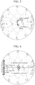
- FIG. 4 is a Smith chart illustrating the frequency dependence of the impedance ⁇ of a Doherty amplifier in which the compensation circuit 9 is included.
- the frequency characteristic of the compensation circuit 9 is switched to the L-characteristic, and thus compensation is performed so as to bring the impedance ⁇ located in the capacitive region closer to the center of the Smith chart.
- the frequency characteristic of the compensation circuit 9 is switched to the C-characteristic, and thus compensation is performed so as to bring the impedance ⁇ located in the inductive region closer to the center of the Smith chart.
- FIG. 5 is an explanatory graph illustrating the frequency dependence of reflection characteristics seen from the output of the combiner 10 toward the combiner 10.
- the compensation circuit 9 performs compensation so as to bring the impedance ⁇ closer to the center of the Smith chart, a wider bandwidth of the Doherty amplifier is achieved as illustrated in FIG. 5 .
- the compensation circuit 9 which causes the impedance seen from the output end 9a of the compensation circuit 9 toward the peaking amplifier 8 to be open within the used frequency range and compensates for the frequency dependence of the impedance seen from the output of the combiner 10 toward the combiner 10 in a state in which the peaking amplifier 8 is not operating, is arranged between the peaking amplifier 8 and the combiner 10, an effect of achieving a wider bandwidth without making the circuit larger in size or more complicated is produced.
- Embodiment 1 the Doherty amplifier in which the compensation circuit 9 is arranged between the peaking amplifier 8 and the combiner 10 has been presented.
- Embodiment 2 a Doherty amplifier in which a compensation circuit 9 is a frequency dependence compensating line having an electrical length of an integer multiple of 180 degrees within the used frequency range will be described.
- FIG. 6 is an explanatory diagram illustrating a frequency dependence compensating line 21, which is a compensation circuit of the Doherty amplifier according to Embodiment 2 in this disclosure.
- N is a natural number.
- FIG. 7 is a Smith chart illustrating the frequency dependence of the impedance ⁇ of the Doherty amplifier in which the frequency dependence compensating line 21 is included.
- the L-characteristic of the frequency dependence compensating line 21 at the same frequency is higher.
- the characteristic impedance Z of the frequency dependence compensating line 21 is determined by the frequency dependences of the carrier amplifier 6 and the 90-degree line 7 and the band characteristics required for the Doherty amplifier.
- the frequency dependence compensating line 21 has an electrical length ⁇ of an integer multiple of 180 degrees at the center frequency in the used frequency range.
- the frequency dependence compensating line 21 only needs to have an electrical length ⁇ of an integer multiple of 180 degrees within the used frequency range, and need not necessarily have the electrical length ⁇ of an integer multiple of 180 degrees at the center frequency.
- Embodiment 3 use of a frequency dependence compensating line 22, which has an electrical length ⁇ of an integer multiple of 180 degrees at the center frequency within the used frequency range and has the same characteristic impedance as the output impedance of the combiner 10, as the compensation circuit 9 will be described.
- FIG. 8 is an explanatory diagram illustrating the frequency dependence compensating line 22, which is a compensation circuit of a Doherty amplifier according to Embodiment 3 in this disclosure.
- FIG. 9 is a Smith chart illustrating the frequency dependence of the impedance ⁇ of the Doherty amplifier in which the frequency dependence compensating line 22 is included.
- the L-characteristic of the frequency dependence compensating line 22 at the same frequency is higher.
- the electrical length ⁇ of the frequency dependence compensating line 22 is determined by the frequency dependences of the carrier amplifier 6 and the 90-degree line 7 and the band characteristics required of the Doherty amplifier.
- the frequency dependence compensating line 22 has an electrical length ⁇ of an integer multiple of 180 degrees at the center frequency in the used frequency range.
- the frequency dependence compensating line 22 only needs to have an electrical length ⁇ of an integer multiple of 180 degrees within the used frequency range, and need not necessarily have the electrical length ⁇ of an integer multiple of 180 degrees at the center frequency.
- Embodiment 1 the Doherty amplifier in which the compensation circuit 9 is arranged between the peaking amplifier 8 and the combiner 10 has been presented.
- a Doherty amplifier including, as the compensation circuit 9, a frequency dependence compensating line 23 in which a plurality of lines each having an electrical length ⁇ of 180 degrees are connected in series and in which the lines having different characteristic impedances from one another will be described.
- FIG. 10 illustrates explanatory diagrams illustrating frequency dependence compensating lines 23, which are each a compensation circuit of the Doherty amplifier according to Embodiment 4 of in this disclosure.
- the compensation amount of the impedance in each of the frequency dependence compensating lines 23 varies according to the characteristic impedance Z of the frequency dependence compensating line 23.
- the L-characteristic of the frequency dependence compensating line 23 at the same frequency is higher.
- the characteristic impedance Z of the frequency dependence compensating line 23 is determined by the frequency dependences of the carrier amplifier 6 and the 90-degree line 7 and the band characteristics required for the Doherty amplifier.
- Embodiment 4 since the frequency dependence compensating line 23, in which a plurality of lines having the electrical length ⁇ of 180 degrees are connected in series and the line have different characteristic impedances from one another, is included as the compensation circuit 9, an effect of achieving a wider bandwidth without making the circuit larger in size or more complicated is produced similarly to Embodiment 1.
- the electrical lengths ⁇ of a plurality of lines in the frequency dependence compensating line 23 are integer multiples of 180 degrees.
- the electrical lengths ⁇ only need to be integer multiples of 180 degrees within the used frequency range, and need not necessarily be integer multiples of 180 degrees at the center frequency in the used frequency range.
- Embodiment 1 the Doherty amplifier in which the compensation circuit 9 is arranged between the peaking amplifier 8 and the combiner 10 has been presented.
- FIG. 11 illustrates explanatory diagrams illustrating frequency dependence compensating lines 24, which are each a compensation circuit of the Doherty amplifier according to Embodiment 5 in this disclosure.
- the characteristic impedance and the electrical length of the line on the input side and the characteristic impedance and the electrical length of the line on the output side of the central line are symmetric in each of the frequency dependence compensating lines 24 illustrated in FIGS. 11A, 11B, and 11C , the impedance at the input and the impedance at the output of each of the frequency dependence compensating lines 24 are matched.
- the compensation amount of the impedance in each of the frequency dependence compensating lines 24 varies according to the characteristic impedance Z of the frequency dependence compensating line 24.
- the L-characteristic of the frequency dependence compensating line 24 at the same frequency is higher.
- the characteristic impedance Z of the frequency dependence compensating line 24 is determined by the frequency dependences of the carrier amplifier 6 and the 90-degree line 7 and the band characteristics required for the Doherty amplifier.
- the frequency dependence compensating line 24 in which a plurality of lines having electrical lengths ⁇ of integer multiples of 90 degrees are connected in series and in which the characteristic impedance and the electrical length of the line present on the input side and the characteristic impedance and the electrical length of the line present on the output side of the line present at the central position among the lines are symmetric, is included as the compensation circuit 9, an effect of achieving a wider bandwidth without making the circuit larger in size or more complicated is produced similarly to Embodiment 1.
- the electrical lengths ⁇ of a plurality of lines in the frequency dependence compensating line 24 are integer multiples of 90 degrees.
- the electrical lengths ⁇ only need to be integer multiples of 90 degrees within the used frequency range, and need not necessarily be integer multiples of 90 degrees at the center frequency in the used frequency range.
- Embodiment 1 the Doherty amplifier in which the compensation circuit 9 is arranged between the peaking amplifier 8 and the combiner 10 has been presented.
- a Doherty amplifier including, as the compensation circuit 9, a frequency dependence compensating line 25 in which a plurality of lines having electrical lengths ⁇ of integer multiples of 90 degrees are connected in series, in which the electrical length of a line present on the input side and the electrical length of a line present on the output side of a line present at the central position in the signal transmitting direction among the lines are symmetric, and in which the characteristic impedance of the line on the input side and the characteristic impedance of the line on the output side are asymmetric will be described.
- FIG. 12 is an explanatory diagram illustrating the frequency dependence compensating line 25, which is a compensation circuit of the Doherty amplifier according to Embodiment 6 in the present disclosure.
- the second line from the left and the second line from the right both have an electrical length ⁇ of 90 degrees, and the electrical lengths are thus symmetric.
- Embodiment 6 since the frequency dependence compensating line 25, in which the electrical length of the line present on the input side and the electrical length of the line present on the output side of the central line present at the central position in the signal transmitting direction are symmetric, is included as the compensation circuit 9, an effect of achieving a wider bandwidth without making the circuit larger in size or more complicated is produced similarly to Embodiment 1.
- the compensation circuit 9 thus includes an impedance converting function.
- Embodiment 1 the Doherty amplifier in which the compensation circuit 9 is arranged between the peaking amplifier 8 and the combiner 10 has been presented.
- a parasitic reactance inside a peaking amplifier 8 may also function as part of a compensation circuit 30.
- FIG. 13 is a configuration diagram illustrating a Doherty amplifier according to Embodiment 7 in the present disclosure, in which the same reference numerals as those in FIG. 1 represent the same or corresponding components and the description thereof will thus not be repeated.
- the compensation circuit 30 is a circuit that causes the impedance seen from an output end 30a of the compensation circuit 30 toward the peaking amplifier 8 to be open within the used frequency range and compensates for the frequency dependence of the impedance seen from the output of the combiner 10 in a state in which the peaking amplifier 8 is not operating, similarly to the compensation circuit 9 in FIG. 1 .
- the compensation circuit 30, however, has such an electrical length that a sum of the electrical length of the compensation circuit 30 and the electrical length of the parasitic reactance inside the peaking amplifier 8 is an integer multiple of 180 degrees within the used frequency range, unlike the compensation circuit 9 of FIG. 1 .
- the compensation circuit 30 includes a compensation unit 31, which has such an electrical length that a sum of the electrical length of the compensation unit 31 and the electrical length of the parasitic reactance inside the peaking amplifier 8 is an integer multiple of 180 degrees within the used frequency range.
- phase correction circuit 5 is arranged on the signal path 3 in the example of FIG. 13
- the phase correction circuit 5 may be arranged on the signal path 4 as long as the electrical length of the signal path 3 and the electrical length of the signal path 4 are made to be equal to each other.
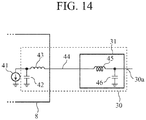
- FIG. 14 is a configuration diagram illustrating the compensation circuit 30 of the Doherty amplifier according to Embodiment 7 in the present disclosure.
- a current source 41 represents a transistor as an amplifying element in the peaking amplifier 8.
- a parasitic capacitance component 42 and a parasitic inductance component 43 are added as the parasitic reactance inside the peaking amplifier 8 to the current source 41 in the peaking amplifier 8.
- a signal path 44 is a path through which a high-frequency signal amplified by the peaking amplifier 8 is transmitted to the compensation unit 31.
- the compensation unit 31 includes an inductor 45 and a capacitor 46.
- the compensation unit 31 includes the inductor 45 and the capacitor 46 is illustrated in FIG. 14 , the compensation unit 31 only needs to have such an electrical length that a sum of the electrical length of the compensation unit 31 and the electrical length of the parasitic reactance inside the peaking amplifier 8 is an integer multiple of 180 degrees within the used frequency range, and the compensation unit may include a line, for example.
- the compensation unit 31 of the compensation circuit 30 has a function of causing the impedance seen from the output end 30a of the compensation circuit 30 toward the peaking amplifier 8 to be open within the used frequency range during back-off operation, and a function of causing the frequency characteristics to be switched to the L-characteristic in a state in which the frequency of a high-frequency signal is in the low-frequency range lower than the center frequency and causing the frequency characteristics to be switched to the C-characteristic in a state in which the frequency of a high-frequency signal is in the high-frequency range higher than the center frequency.
- the frequency characteristics of the compensation unit 31 are switched to the L-characteristic, and thus, compensation is performed so as to bring the impedance ⁇ located in the capacitive region closer to the center of the Smith chart.
- the frequency characteristics of the compensation unit 31 are switched to the C-characteristic, and thus, compensation is performed so as to bring the impedance ⁇ located in the inductive region closer to the center of the Smith chart.
- the parasitic reactance inside the peaking amplifier 8 also functions as part of the compensation circuit 30, and since the compensation unit 31 of the compensation circuit 30 causes the impedance seen from the output end 30a toward the peaking amplifier 8 to be open within the used frequency range and compensates for the frequency dependence of the impedance seen from the output of the combiner 10 toward combiner 10 in the state in which the peaking amplifier 8 is not operating, an effect of achieving a wider bandwidth without making the circuit larger in size or more complicated is produced, similarly to Embodiment 1.
- Embodiments 1-7 described above it is assumed that distributed constant lines compose the phase correction circuit 5, the 90-degree line 7, and the compensation circuits 9 and 30.
- lumped parameter elements may compose the phase correction circuit 5, the 90-degree line 7, and the compensation circuits 9 and 30.
- One or more disclosed embodiments are suitable for a Doherty amplifier in which a carrier amplifier and a peaking amplifier are connected in parallel.
Landscapes
- Engineering & Computer Science (AREA)
- Power Engineering (AREA)
- Amplifiers (AREA)
Abstract
Description
- The present disclosure relates to Doherty amplifiers in which a carrier amplifier and a peaking amplifier are connected in parallel.
- In recent years, Doherty amplifiers that achieve highly efficient operation have been proposed as amplifiers for communication.
- A Doherty amplifier includes a carrier amplifier and a peaking amplifier connected in parallel, and a 90-degree line for performing load modulation loaded at the output of the carrier amplifier, to achieve highly efficient operation during back-off operation in which output power is lower than saturation power. The back-off operation refers to a state in which the peaking amplifier is not operating.
- In the Doherty amplifier, however, the electrical length of the 90-degree line may deviate, in principle of operation, from 90 degrees owing to the frequency dependence of the 90-degree line loaded at the output of the carrier amplifier, thus resulting in narrow bandwidth of the operation.
-
Patent Literature 1 mentioned below discloses a Doherty amplifier including a plurality of lines having different electrical lengths at the output of a carrier amplifier, and including a control mechanism for selecting a line to be connected to the output of the carrier amplifier from the plurality of lines having different electrical lengths according to the frequency of an input signal. - The control mechanism serves to make the electrical length of a line at the output of the carrier amplifier closer to 90 degrees.
- Patent Literature 1:
JP 2006-345341 A - Since the Doherty amplifier of the related art is configured as described above, the electrical length of a line at the output of the carrier amplifier can be made closer to 90 degrees. However, because a detection mechanism for detecting the frequency of an input signal and the control mechanism for selecting a line to be connected with the output of the carrier amplifier need to be included, there has been a problem of making the circuit larger in size and more complicated.
- In addition, there has also been a problem in that no selected line can achieve a wider bandwidth in such a case in which the frequency bandwidth of an input signal is wider than the bandwidth covered by each line provided at the output of the carrier amplifier.
- One or more embodiments according to this disclosure have been made to solve such problems as described above, and an object thereof is to achieve a Doherty amplifier capable of achieving a wider bandwidth without making a circuit larger in size or more complicated.
- A Doherty amplifier according to the present disclosure includes: a divider for dividing a signal to be amplified; a carrier amplifier for amplifying one of signals obtained by division by the divider; a 90-degree line having one end connected with an output of the carrier amplifier; a peaking amplifier for amplifying another of the signals obtained by the division by the divider; and a combiner for combining a signal passing through the 90-degree line and a signal obtained by amplification by the peaking amplifier, and outputting a resultant combined signal, wherein a compensation circuit, arranged between the peaking amplifier and the combiner, for causing an impedance seen from an output end of the compensation circuit toward the peaking amplifier to be open within a used frequency range and compensating for frequency dependence of an impedance seen from an output of the combiner toward the combiner, in a state in which the peaking amplifier is not operating.
- According to a Doherty amplifier disclosed by this application, since the compensation circuit, which causes the impedance seen from the output end of the compensation circuit toward the peaking amplifier to be open within the used frequency range and compensates for the frequency dependence of the impedance seen from the output of the combiner toward the combiner in a state in which the peaking amplifier is not operating, is arranged between the peaking amplifier and the combiner, an effect of achieving a wider bandwidth without making the circuit larger in size or more complicated is produced.
-
-
FIG. 1 is a configuration diagram of a Doherty amplifier according toEmbodiment 1 in this disclosure. -
FIG. 2 is a configuration diagram illustrating a Doherty amplifier in a case in which nocompensation circuit 9 is included. -
FIG. 3 is a Smith chart illustrating the frequency dependence of the impedance Γ of a Doherty amplifier in which nocompensation circuit 9 is included. -
FIG. 4 is a Smith chart illustrating the frequency dependence of the impedance Γ of a Doherty amplifier in which acompensation circuit 9 is included. -
FIG. 5 is an explanatory graph illustrating the frequency dependence of reflection characteristics seen from an output of acombiner 10 toward thecombiner 10. -
FIG. 6 is an explanatory diagram illustrating a frequencydependence compensating line 21, which is a compensation circuit of a Doherty amplifier according toEmbodiment 2 in this disclosure. -
FIG. 7 is a Smith chart illustrating the frequency dependence of the impedance Γ of the Doherty amplifier in which the frequencydependence compensating line 21 is included. -
FIG. 8 is an explanatory diagram illustrating a frequencydependence compensating line 22, which is a compensation circuit of a Doherty amplifier according toEmbodiment 3 in this disclosure. -
FIG. 9 is a Smith chart illustrating the frequency dependence of the impedance Γ of the Doherty amplifier in which the frequencydependence compensating line 22 is included. -
FIG. 10A is an explanatory diagram illustrating a frequencydependence compensating line 23 in which a line having an electrical length θ of 180 degrees and a characteristic impedance Z = b and a line having an electrical length θ of 180 degrees and a characteristic impedance Z = c are connected in series; andFIG. 10B is an explanatory diagram illustrating a frequencydependence compensating line 23 in which a line having an electrical length θ of 180 degrees and a characteristic impedance Z = b, a line having an electrical length θ of 180 degrees and a characteristic impedance Z = c, and a line having an electrical length θ of 180 degrees and a characteristic impedance Z = d are connected in series. -
FIG. 11A is an explanatory diagram illustrating a frequencydependence compensating line 24 in which a line having an electrical length θ of 90 degrees and a characteristic impedance Z = b, a line having an electrical length θ of 180 degrees and a characteristic impedance Z = c, and a line having an electrical length θ of 90 degrees and a characteristic impedance Z = b are connected in series;FIG. 11B is an explanatory diagram illustrating a frequencydependence compensating line 24 in which a line having an electrical length θ of 90 degrees and a characteristic impedance Z = d, a line having an electrical length θ of 180 degrees and a characteristic impedance Z = e, and a line having an electrical length θ of 90 degrees and a characteristic impedance Z = d are connected in series; andFIG. 11C is an explanatory diagram illustrating a frequencydependence compensating line 24 in which a line having an electrical length θ of 180 degrees and a characteristic impedance Z = f, a line having an electrical length θ of 90 degrees and a characteristic impedance Z = d, a line having an electrical length θ of 180 degrees and a characteristic impedance Z = e, a line having an electrical length θ of 90 degrees and a characteristic impedance Z = d, and a line having an electrical length θ of 180 degrees and a characteristic impedance Z = f are connected in series. -
FIG. 12 is an explanatory diagram illustrating a frequencydependence compensating line 25, which is a compensation circuit of a Doherty amplifier according toEmbodiment 6 in this disclosure. -
FIG. 13 is a configuration diagram illustrating a Doherty amplifier according toEmbodiment 7 in this disclosure. -
FIG. 14 is a configuration diagram illustrating acompensation circuit 30 of a Doherty amplifier according toEmbodiment 7 in this disclosure. - To describe this application in more detail, embodiments according to this disclosure will now be described with reference to the accompanying drawings.
-
FIG. 1 is a configuration diagram illustrating a Doherty amplifier according toEmbodiment 1 in this disclosure. - In
FIG. 1 , aninput terminal 1 is a terminal to which a high-frequency signal, such as a microwave or a millimeter wave, is input as a signal to be amplified. - A
divider 2 divides a high-frequency signal input from theinput terminal 1, outputs one of high-frequency signals obtained by the division to asignal path 3, and outputs the other of the high-frequency signals to asignal path 4. - The
signal path 3 is a path from thedivider 2 to a combiner 10 via acarrier amplifier 6. - The
signal path 4 is a path from thedivider 2 to the combiner 10 via a peakingamplifier 8. - A
phase correction circuit 5 is a circuit inserted on thesignal path 3 to make the electrical length of thesignal path 3 and the electrical length of thesignal path 4 equal to each other. - While the
phase correction circuit 5 is provided in thesignal path 3 in the example ofFIG. 1 , thephase correction circuit 5 may be provided in thesignal path 4 as long as the electrical length of thesignal path 3 and the electrical length of thesignal path 4 are made to be equal to each other. - The
carrier amplifier 6 is an amplifying element that amplifies the high-frequency signal passed through thephase correction circuit 5. - A 90-
degree line 7 is a line having an electrical length of 90 degrees with one end connected with an output of thecarrier amplifier 6 and the other end connected with thecombiner 10. - The peaking
amplifier 8 is an amplifying element that is provided in thesignal path 4 and amplifies the high-frequency signal obtained by the division by thedivider 2. - A
compensation circuit 9 is a circuit that is provided between thepeaking amplifier 8 and thecombiner 10, causes the impedance seen from anoutput end 9a of thecompensation circuit 9 toward the peakingamplifier 8 to be open within a used frequency range and compensates for the frequency dependence of the impedance seen from an output of thecombiner 10 toward thecombiner 10, in a state in which thepeaking amplifier 8 is not operating. - Specifically, the
compensation circuit 9 is a circuit that, when the impedance seen from the output of thecombiner 10 toward thecombiner 10 is in the capacitive region, performs compensation to bring the impedance closer to a boundary between the capacitive region and the inductive region, and that, when the impedance seen from the output of thecombiner 10 toward thecombiner 10 is in the inductive region, performs compensation to bring the impedance closer to the boundary between the capacitive region and the inductive region. - Note that within the used frequency range refers to within a range of frequency used by the Doherty amplifier in
FIG. 1 . - The
combiner 10 combines the high-frequency signal passed through the 90-degree line 7 and the high-frequency signal passed through thecompensation circuit 9 at asignal combining point 10a, and outputs the resulting combined high-frequency signal to anoutput terminal 11. - The signal combining
point 10a is a connecting point at which thesignal path 3 and thesignal path 4 are connected with each other. - Note that the
combiner 10 is simply a circuit in which thesignal path 3 and thesignal path 4 are connected at thesignal combining point 10a and which has a signal path from thesignal combining point 10a to theoutput terminal 11, and it is not a combiner like a so-called Wilkinson divider. - The
output terminal 11 is a terminal that outputs the combined high-frequency signal output from thecombiner 10 to the outside. - Next, operation will be explained.
- The
divider 2 divides a high-frequency signal input from theinput terminal 1, outputs one of high-frequency signals obtained by the division to thesignal path 3, and outputs the other of the high-frequency signals to thesignal path 4. - The high-frequency signal output from the
divider 2 to thesignal path 3 is input to thephase correction circuit 5. - The
phase correction circuit 5 has such an electrical length that the electrical length of thesignal path 3 and the electrical length of thesignal path 4 are equal to each other. The electrical length of thesignal path 3 and the electrical length of thesignal path 4 are thus made to be equal to each other by thephase correction circuit 5. - The
carrier amplifier 6 amplifies the high-frequency signal passed through thephase correction circuit 5. - The high-frequency signal amplified by the
carrier amplifier 6 passes through the 90-degree line 7 with an electrical length of 90 degrees and then reaches thecombiner 10. - The peaking
amplifier 8 amplifies the high-frequency signal obtained by the division by thedivider 2. - The high-frequency signal amplified by the peaking
amplifier 8 passes through thecompensation circuit 9 and then reaches thecombiner 10. - The
combiner 10 combines the high-frequency signal passed through the 90-degree line 7 and the high-frequency signal passed through thecompensation circuit 9, and outputs the resulting combined high-frequency signal to theoutput terminal 11. - Hereinafter, the operation of the
compensation circuit 9 will be explained more specifically. -
FIG. 2 is a configuration diagram illustrating a Doherty amplifier in a case in which nocompensation circuit 9 is included. - The Doherty amplifier of
FIG. 2 is an example in which thecompensation circuit 9 is not included. Because of this, the electrical length of thesignal path 4 inFIG. 2 is shorter than that of thesignal path 4 in the Doherty amplifier shown inFIG. 1 , and thus thephase correction circuit 5 is provided in thesignal path 4 in the example. -
FIG. 2 illustrates impedance transformation in a state in which the peakingamplifier 8 is not operating (hereinafter referred to as "during back-off operation." - When the output impedance of the Doherty amplifier is Ropt, the output load of the
carrier amplifier 6 is typically twice the output impedance Ropt of the Doherty amplifier during back-off operation. - Thus, in
FIG. 2 , the impedance seen from the output of thecarrier amplifier 6 toward thecarrier amplifier 6 is 2 × Ropt. - The peaking
amplifier 8 is not operating, and the output impedance of the peakingamplifier 8 is open. - In addition, in
FIG. 2 , the characteristic impedance of the 90-degree line 7 is Ropt, and the electrical length of the 90-degree line 7 is 90 degrees at the center frequency in the used frequency range of the Doherty amplifier. - In this case, the frequency dependence of the impedance Γ seen from the output of the
combiner 10 toward thecombiner 10 is expressed as inFIG. 3 . -
FIG. 3 is a Smith chart illustrating the frequency dependence of the impedance Γ of a Doherty amplifier in which nocompensation circuit 9 is included. - In a state in which the frequency of a high-frequency signal is equal to the center frequency in the use frequency range of the Doherty amplifier, the impedance Γ is located at the center of the Smith chart, that is, on the horizontal axis of the Smith chart.
- In a state in which the frequency of a high-frequency signal is in a low-frequency range lower than the center frequency, however, the electrical length of the 90-
degree line 7 is shorter than 90 degrees, and the impedance Γ is thus located in the capacitive region. - In addition, in a state in which the frequency of a high-frequency signal is in a high-frequency range higher than the center frequency, the electrical length of the 90-
degree line 7 is longer than 90 degrees, and the impedance Γ is thus located in the inductive region. - As a result, as the frequency of the high-frequency signal is farther away from the center frequency, reflection characteristics are deteriorated.
- Next, operation in a case where the Doherty amplifier includes the
compensation circuit 9 as illustrated inFIG. 1 will be described. - In this case as well, assume that the characteristic impedance of the 90-
degree line 7 is Ropt, and the electrical length of the 90-degree line 7 is 90 degrees at the center frequency in the used frequency range of the Doherty amplifier. - The
compensation circuit 9 has a function of causing the impedance seen from theoutput end 9a of thecompensation circuit 9 toward the peakingamplifier 8 to be open within the used frequency range, and a function of causing the frequency characteristics to be switched to inductive (hereinafter referred to as "L-characteristic") in a state in which the frequency of a high-frequency signal is in the low-frequency range lower than the center frequency, and causing the frequency characteristics to be switched to capacitive (hereinafter referred to as "C-characteristic") in a state in which the frequency of a high-frequency signal is in the high-frequency range higher than the center frequency. -
FIG. 4 is a Smith chart illustrating the frequency dependence of the impedance Γ of a Doherty amplifier in which thecompensation circuit 9 is included. - In the state in which the frequency of a high-frequency signal is in the low-frequency range lower than the center frequency, the frequency characteristic of the
compensation circuit 9 is switched to the L-characteristic, and thus compensation is performed so as to bring the impedance Γ located in the capacitive region closer to the center of the Smith chart. - In contrast, in the state in which the frequency of a high-frequency signal is in the high-frequency range higher than the center frequency, the frequency characteristic of the
compensation circuit 9 is switched to the C-characteristic, and thus compensation is performed so as to bring the impedance Γ located in the inductive region closer to the center of the Smith chart. -
FIG. 5 is an explanatory graph illustrating the frequency dependence of reflection characteristics seen from the output of thecombiner 10 toward thecombiner 10. - Since the
compensation circuit 9 performs compensation so as to bring the impedance Γ closer to the center of the Smith chart, a wider bandwidth of the Doherty amplifier is achieved as illustrated inFIG. 5 . - As is clear from the description above, according to
Embodiment 1, since thecompensation circuit 9, which causes the impedance seen from theoutput end 9a of thecompensation circuit 9 toward the peakingamplifier 8 to be open within the used frequency range and compensates for the frequency dependence of the impedance seen from the output of thecombiner 10 toward thecombiner 10 in a state in which the peakingamplifier 8 is not operating, is arranged between the peakingamplifier 8 and thecombiner 10, an effect of achieving a wider bandwidth without making the circuit larger in size or more complicated is produced. - In
Embodiment 1 described above, the Doherty amplifier in which thecompensation circuit 9 is arranged between the peakingamplifier 8 and thecombiner 10 has been presented. InEmbodiment 2, a Doherty amplifier in which acompensation circuit 9 is a frequency dependence compensating line having an electrical length of an integer multiple of 180 degrees within the used frequency range will be described. -
FIG. 6 is an explanatory diagram illustrating a frequencydependence compensating line 21, which is a compensation circuit of the Doherty amplifier according toEmbodiment 2 in this disclosure. - In
FIG. 6 , the frequencydependence compensating line 21 is a line having an electrical length θ of an integer multiple of 180 degrees at the center frequency in the used frequency range and having a characteristic impedance Z = a. InFIG. 6 , N is a natural number. -
FIG. 7 is a Smith chart illustrating the frequency dependence of the impedance Γ of the Doherty amplifier in which the frequencydependence compensating line 21 is included. -
FIG. 7 illustrates an example in which the electrical length θ of the frequencydependence compensating line 21 is 360 degrees (= 2 × 180 degrees) within the used frequency range. In other words,FIG. 7 illustrates an example in which N = 2. - In a state in which the frequency of a high-frequency signal is in the low-frequency range lower than the center frequency, compensation is performed so as to bring the impedance Γ located in the capacitive region closer to the center of the Smith chart by using the L-characteristic of the frequency
dependence compensating line 21. - In contrast, in a state in which the frequency of the high-frequency signal is in the high-frequency range higher than the center frequency, compensation is performed so as to bring the impedance Γ closer to the center of the Smith chart by using the C-characteristic of the frequency
dependence compensating line 21. - It can be seen in
FIG. 7 that the compensation amount of the impedance varies according to the characteristic impedance Z of the frequencydependence compensating line 21. - As the characteristic impedance Z of the frequency
dependence compensating line 21 is smaller, the L-characteristic of the frequencydependence compensating line 21 at the same frequency is higher. - The characteristic impedance Z of the frequency
dependence compensating line 21 is determined by the frequency dependences of thecarrier amplifier 6 and the 90-degree line 7 and the band characteristics required for the Doherty amplifier. - As is clear from the description above, according to
Embodiment 2, since the frequencydependence compensating line 21 having an electrical length of an integer multiple of 180 degrees within the used frequency range is included as thecompensation circuit 9, an effect of achieving a wider bandwidth without making the circuit larger in size or more complicated is produced similarly toEmbodiment 1. - While an example in which the frequency
dependence compensating line 21 has an electrical length θ of an integer multiple of 180 degrees at the center frequency in the used frequency range has been presented inEmbodiment 2, the frequencydependence compensating line 21 only needs to have an electrical length θ of an integer multiple of 180 degrees within the used frequency range, and need not necessarily have the electrical length θ of an integer multiple of 180 degrees at the center frequency. - In
Embodiment 2 described above, use of the frequencydependence compensating line 21, which has an electrical length θ of an integer multiple of 180 degrees at the center frequency within the used frequency range and has a characteristic impedance Z = a, as thecompensation circuit 9 has been presented. InEmbodiment 3, use of a frequencydependence compensating line 22, which has an electrical length θ of an integer multiple of 180 degrees at the center frequency within the used frequency range and has the same characteristic impedance as the output impedance of thecombiner 10, as thecompensation circuit 9 will be described. -
FIG. 8 is an explanatory diagram illustrating the frequencydependence compensating line 22, which is a compensation circuit of a Doherty amplifier according toEmbodiment 3 in this disclosure. - In
FIG. 8 , the frequencydependence compensating line 22 is a line having an electrical length θ of an integer multiple of 180 degrees at the center frequency in the used frequency range and having the same characteristic impedance Z = Ropt as the output impedance of thecombiner 10. -
FIG. 9 is a Smith chart illustrating the frequency dependence of the impedance Γ of the Doherty amplifier in which the frequencydependence compensating line 22 is included. - In a state in which the frequency of a high-frequency signal is in the low-frequency range lower than the center frequency, compensation is performed so as to bring the impedance Γ located in the capacitive region closer to the center of the Smith chart by using the L-characteristic of the frequency
dependence compensating line 22. - In contrast, in a state in which the frequency of the high-frequency signal is in the high-frequency range higher than the center frequency, compensation is performed so as to bring the impedance Γ closer to the center of the Smith chart by using the C-characteristic of the frequency
dependence compensating line 22. - It can be seen in
FIG. 9 that the compensation amount of the impedance varies according to the electrical length θ of the frequencydependence compensating line 22. - As the electrical length θ of the frequency
dependence compensating line 22 is longer, the L-characteristic of the frequencydependence compensating line 22 at the same frequency is higher. - The electrical length θ of the frequency
dependence compensating line 22 is determined by the frequency dependences of thecarrier amplifier 6 and the 90-degree line 7 and the band characteristics required of the Doherty amplifier. - As is clear from the description above, according to
Embodiment 3, since the frequencydependence compensating line 22 having an electrical length of an integer multiple of 180 degrees within the used frequency range is included as thecompensation circuit 9, an effect of achieving a wider bandwidth without making the circuit larger in size or more complicated is produced similarly toEmbodiment 1. - While an example in which the frequency
dependence compensating line 22 has an electrical length θ of an integer multiple of 180 degrees at the center frequency in the used frequency range has been presented inEmbodiment 3, the frequencydependence compensating line 22 only needs to have an electrical length θ of an integer multiple of 180 degrees within the used frequency range, and need not necessarily have the electrical length θ of an integer multiple of 180 degrees at the center frequency. - In
Embodiment 1 described above, the Doherty amplifier in which thecompensation circuit 9 is arranged between the peakingamplifier 8 and thecombiner 10 has been presented. InEmbodiment 4, a Doherty amplifier including, as thecompensation circuit 9, a frequencydependence compensating line 23 in which a plurality of lines each having an electrical length θ of 180 degrees are connected in series and in which the lines having different characteristic impedances from one another will be described. -
FIG. 10 illustrates explanatory diagrams illustrating frequencydependence compensating lines 23, which are each a compensation circuit of the Doherty amplifier according toEmbodiment 4 of in this disclosure. -
FIG. 10A is an explanatory diagram illustrating a frequencydependence compensating line 23 in which a line having an electrical length θ of 180 degrees and a characteristic impedance Z = b and a line having an electrical length θ of 180 degrees and a characteristic impedance Z = c are connected in series. -
FIG. 10B is an explanatory diagram illustrating a frequencydependence compensating line 23 in which a line having an electrical length θ of 180 degrees and a characteristic impedance Z = b, a line having an electrical length θ of 180 degrees and a characteristic impedance Z = c, and a line having an electrical length θ of 180 degrees and a characteristic impedance Z = d are connected in series. - In either of the frequency
dependence compensating lines 23 illustrated inFIGS. 10A and 10B , although the lines that are connected are different in characteristic impedance Z, because the lines all having the electrical length θ of 180 degrees are connected in series, the impedance at the input and the impedance at the output of each of the frequencydependence compensating lines 23 are matched. - In a state in which the frequency of a high-frequency signal is in the low-frequency range lower than the center frequency, compensation is performed so as to bring the impedance Γ located in the capacitive region closer to the center of the Smith chart by using the L-characteristic of the frequency
dependence compensating lines 23. - In contrast, in a state in which the frequency of the high-frequency signal is in the high-frequency range higher than the center frequency, compensation is performed so as to bring the impedance Γ closer to the center of the Smith chart by using the C-characteristic of the frequency
dependence compensating lines 23. - The compensation amount of the impedance in each of the frequency
dependence compensating lines 23 varies according to the characteristic impedance Z of the frequencydependence compensating line 23. - As the characteristic impedance Z of the frequency
dependence compensating line 23 is smaller, the L-characteristic of the frequencydependence compensating line 23 at the same frequency is higher. - The characteristic impedance Z of the frequency
dependence compensating line 23 is determined by the frequency dependences of thecarrier amplifier 6 and the 90-degree line 7 and the band characteristics required for the Doherty amplifier. - As is clear from the description above, according to
Embodiment 4, since the frequencydependence compensating line 23, in which a plurality of lines having the electrical length θ of 180 degrees are connected in series and the line have different characteristic impedances from one another, is included as thecompensation circuit 9, an effect of achieving a wider bandwidth without making the circuit larger in size or more complicated is produced similarly toEmbodiment 1. - While an example in which the electrical lengths θ of a plurality of lines in the frequency
dependence compensating line 23 are integer multiples of 180 degrees has been presented inEmbodiment 4, the electrical lengths θ only need to be integer multiples of 180 degrees within the used frequency range, and need not necessarily be integer multiples of 180 degrees at the center frequency in the used frequency range. - In
Embodiment 1 described above, the Doherty amplifier in which thecompensation circuit 9 is arranged between the peakingamplifier 8 and thecombiner 10 has been presented. InEmbodiment 5, a Doherty amplifier including, as thecompensation circuit 9, a frequencydependence compensating line 24 in which a plurality of lines having electrical lengths θ of integer multiples of 90 degrees are connected in series and in which the characteristic impedance and the electrical length of a line present on the input side of a line present at the central position in the signal transmitting direction and the characteristic impedance and the electrical length of a line present on the output side of the line present at the central position among the lines are symmetric will be described. -
FIG. 11 illustrates explanatory diagrams illustrating frequencydependence compensating lines 24, which are each a compensation circuit of the Doherty amplifier according toEmbodiment 5 in this disclosure. -
FIG. 11A is an explanatory diagram illustrating a frequencydependence compensating line 24 in which a line having an electrical length θ of 90 degrees and a characteristic impedance Z = b, a line having an electrical length θ of 180 degrees and a characteristic impedance Z = c, and a line having an electrical length θ of 90 degrees and a characteristic impedance Z = b are connected in series. -
FIG. 11B is an explanatory diagram illustrating a frequencydependence compensating line 24 in which a line having an electrical length θ of 90 degrees and a characteristic impedance Z = d, a line having an electrical length θ of 180 degrees and a characteristic impedance Z = e, and a line having an electrical length θ of 90 degrees and a characteristic impedance Z = d are connected in series. -
FIG. 11C is an explanatory diagram illustrating a frequencydependence compensating line 24 in which a line having an electrical length θ of 180 degrees and a characteristic impedance Z = f, a line having an electrical length θ of 90 degrees and a characteristic impedance Z = d, a line having an electrical length θ of 180 degrees and a characteristic impedance Z = e, a line having an electrical length θ of 90 degrees and a characteristic impedance Z = d, and a line having an electrical length θ of 180 degrees and a characteristic impedance Z = f are connected in series. - In the frequency
dependence compensating line 24 illustrated inFIG. 11A , a line present at the central position in the signal transmitting direction is the line having an electrical length θ of 180 degrees and a characteristic impedance Z = c (hereinafter referred to as a "central line"), and the characteristic impedances and the electrical lengths of the line on the left and the line on the right of the central line inFIG. 11A are symmetric with respect to the central line. - Specifically, the line on the left and the line on the right both have an electrical length θ of 90 degrees and a characteristic impedance Z = b.
- In addition, in the frequency
dependence compensating line 24 illustrated inFIG. 11B , a line present at the central position in the signal transmitting direction is the line having an electrical length θ of 180 degrees and a characteristic impedance Z = e (hereinafter referred to as a "central line"), and the characteristic impedances and the electrical lengths of the line on the left and the line on the right of the central line inFIG. 11B are symmetric with respect to the central line. - Specifically, the line on the left and the line on the right both have an electrical length θ of 90 degrees and a characteristic impedance Z = d.
- In the frequency
dependence compensating line 24 illustrated inFIG. 11C , a line present at the central position in the signal transmitting direction is the line having an electrical length θ of 180 degrees and a characteristic impedance Z = e (hereinafter referred to as a "central line"), and the characteristic impedances and the electrical lengths of the line on the left and the line on the right of the central line inFIG. 11C are symmetric with respect to the central line. - Specifically, the leftmost line and the rightmost line both have an electrical length θ of 180 degrees and a characteristic impedance Z = f.
- In addition, the second line from the left and the second line from the right both have an electrical length θ of 90 degrees and a characteristic impedance Z = d.
- Thus, since the characteristic impedance and the electrical length of the line on the input side and the characteristic impedance and the electrical length of the line on the output side of the central line are symmetric in each of the frequency
dependence compensating lines 24 illustrated inFIGS. 11A, 11B, and 11C , the impedance at the input and the impedance at the output of each of the frequencydependence compensating lines 24 are matched. - In a state in which the frequency of a high-frequency signal is in the low-frequency range lower than the center frequency, compensation is performed so as to bring the impedance Γ located in the capacitive region closer to the center of the Smith chart by using the L-characteristic of the frequency
dependence compensating lines 24. - In contrast, in a state in which the frequency of the high-frequency signal is in the high-frequency range higher than the center frequency, compensation is performed so as to bring the impedance Γ closer to the center of the Smith chart by using the C-characteristic of the frequency
dependence compensating lines 24. - The compensation amount of the impedance in each of the frequency
dependence compensating lines 24 varies according to the characteristic impedance Z of the frequencydependence compensating line 24. - As the characteristic impedance Z of the frequency
dependence compensating line 24 is smaller, the L-characteristic of the frequencydependence compensating line 24 at the same frequency is higher. - The characteristic impedance Z of the frequency
dependence compensating line 24 is determined by the frequency dependences of thecarrier amplifier 6 and the 90-degree line 7 and the band characteristics required for the Doherty amplifier. - As is clear from the description above, according to
Embodiment 5, since the frequencydependence compensating line 24, in which a plurality of lines having electrical lengths θ of integer multiples of 90 degrees are connected in series and in which the characteristic impedance and the electrical length of the line present on the input side and the characteristic impedance and the electrical length of the line present on the output side of the line present at the central position among the lines are symmetric, is included as thecompensation circuit 9, an effect of achieving a wider bandwidth without making the circuit larger in size or more complicated is produced similarly toEmbodiment 1. - While an example in which the electrical lengths θ of a plurality of lines in the frequency
dependence compensating line 24 are integer multiples of 90 degrees has been presented inEmbodiment 5, the electrical lengths θ only need to be integer multiples of 90 degrees within the used frequency range, and need not necessarily be integer multiples of 90 degrees at the center frequency in the used frequency range. - In
Embodiment 1 described above, the Doherty amplifier in which thecompensation circuit 9 is arranged between the peakingamplifier 8 and thecombiner 10 has been presented. InEmbodiment 6, a Doherty amplifier including, as thecompensation circuit 9, a frequencydependence compensating line 25 in which a plurality of lines having electrical lengths θ of integer multiples of 90 degrees are connected in series, in which the electrical length of a line present on the input side and the electrical length of a line present on the output side of a line present at the central position in the signal transmitting direction among the lines are symmetric, and in which the characteristic impedance of the line on the input side and the characteristic impedance of the line on the output side are asymmetric will be described. -
FIG. 12 is an explanatory diagram illustrating the frequencydependence compensating line 25, which is a compensation circuit of the Doherty amplifier according toEmbodiment 6 in the present disclosure. - Specifically,
FIG. 12 is an explanatory diagram illustrating the frequencydependence compensating line 25 in which a line having an electrical length θ of 180 degrees and a characteristic impedance Z = f, a line having an electrical length θ of 90 degrees and a characteristic impedance Z = g, a line having an electrical length θ of 180 degrees and a characteristic impedance Z = e, a line having an electrical length θ of 90 degrees and a characteristic impedance Z = d, and a line having an electrical length θ of 180 degrees and a characteristic impedance Z = f are connected in series. - In the frequency
dependence compensating line 24 illustrated inFIG. 12 , a line present at the central position in the signal transmitting direction is the line having an electrical length θ of 180 degrees and a characteristic impedance Z = e (hereinafter referred to as a "central line"), and the electrical lengths of the line on the left and the line on the right of the central line inFIG. 12 are symmetric with respect to the central line. - Specifically, the leftmost line and the rightmost line both have an electrical length θ of 180 degrees and a characteristic impedance Z = f, and the electrical lengths and the characteristic impedances are thus symmetric.
- The second line from the left and the second line from the right both have an electrical length θ of 90 degrees, and the electrical lengths are thus symmetric. The second line from the left, however, has a characteristic impedance Z = g while the second line from the right has a characteristic impedance Z = d, and the characteristic impedances are thus asymmetric.
- In a state in which the frequency of a high-frequency signal is in the low-frequency range lower than the center frequency, compensation is performed so as to bring the impedance Γ located in the capacitive region closer to the center of the Smith chart by using the L-characteristic of the frequency
dependence compensating lines 25. - In contrast, in a state in which the frequency of the high-frequency signal is in the high-frequency range higher than the center frequency, compensation is performed so as to bring the impedance Γ located in the inductive region closer to the center of the Smith chart by using the C-characteristic of the frequency
dependence compensating lines 25. - In
Embodiment 6, since the frequencydependence compensating line 25, in which the electrical length of the line present on the input side and the electrical length of the line present on the output side of the central line present at the central position in the signal transmitting direction are symmetric, is included as thecompensation circuit 9, an effect of achieving a wider bandwidth without making the circuit larger in size or more complicated is produced similarly toEmbodiment 1. - In addition, in
Embodiment 6, since the characteristic impedance of the line present on the input side and the characteristic impedance of the line present on the output side of the central line are asymmetric, the impedance at the input and the impedance at the output of the frequencydependence compensating line 25 are not equal to each other. Thecompensation circuit 9 thus includes an impedance converting function. - In
Embodiment 1 described above, the Doherty amplifier in which thecompensation circuit 9 is arranged between the peakingamplifier 8 and thecombiner 10 has been presented. InEmbodiment 7, a parasitic reactance inside a peakingamplifier 8 may also function as part of acompensation circuit 30. -
FIG. 13 is a configuration diagram illustrating a Doherty amplifier according toEmbodiment 7 in the present disclosure, in which the same reference numerals as those inFIG. 1 represent the same or corresponding components and the description thereof will thus not be repeated. - The
compensation circuit 30 is a circuit that causes the impedance seen from anoutput end 30a of thecompensation circuit 30 toward the peakingamplifier 8 to be open within the used frequency range and compensates for the frequency dependence of the impedance seen from the output of thecombiner 10 in a state in which the peakingamplifier 8 is not operating, similarly to thecompensation circuit 9 inFIG. 1 . - The
compensation circuit 30, however, has such an electrical length that a sum of the electrical length of thecompensation circuit 30 and the electrical length of the parasitic reactance inside the peakingamplifier 8 is an integer multiple of 180 degrees within the used frequency range, unlike thecompensation circuit 9 ofFIG. 1 . - Specifically, the
compensation circuit 30 includes acompensation unit 31, which has such an electrical length that a sum of the electrical length of thecompensation unit 31 and the electrical length of the parasitic reactance inside the peakingamplifier 8 is an integer multiple of 180 degrees within the used frequency range. - While the
phase correction circuit 5 is arranged on thesignal path 3 in the example ofFIG. 13 , thephase correction circuit 5 may be arranged on thesignal path 4 as long as the electrical length of thesignal path 3 and the electrical length of thesignal path 4 are made to be equal to each other. -
FIG. 14 is a configuration diagram illustrating thecompensation circuit 30 of the Doherty amplifier according toEmbodiment 7 in the present disclosure. - In
FIG. 14 , acurrent source 41 represents a transistor as an amplifying element in the peakingamplifier 8. - A
parasitic capacitance component 42 and aparasitic inductance component 43 are added as the parasitic reactance inside the peakingamplifier 8 to thecurrent source 41 in the peakingamplifier 8. - A
signal path 44 is a path through which a high-frequency signal amplified by the peakingamplifier 8 is transmitted to thecompensation unit 31. - The
compensation unit 31 includes aninductor 45 and acapacitor 46. - While an example in which the
compensation unit 31 includes theinductor 45 and thecapacitor 46 is illustrated inFIG. 14 , thecompensation unit 31 only needs to have such an electrical length that a sum of the electrical length of thecompensation unit 31 and the electrical length of the parasitic reactance inside the peakingamplifier 8 is an integer multiple of 180 degrees within the used frequency range, and the compensation unit may include a line, for example. - Similarly to the
compensation circuit 9 ofFIG. 1 , thecompensation unit 31 of thecompensation circuit 30 has a function of causing the impedance seen from theoutput end 30a of thecompensation circuit 30 toward the peakingamplifier 8 to be open within the used frequency range during back-off operation, and a function of causing the frequency characteristics to be switched to the L-characteristic in a state in which the frequency of a high-frequency signal is in the low-frequency range lower than the center frequency and causing the frequency characteristics to be switched to the C-characteristic in a state in which the frequency of a high-frequency signal is in the high-frequency range higher than the center frequency. - Thus, In the state in which the frequency of a high-frequency signal is in the low-frequency range lower than the center frequency, the frequency characteristics of the
compensation unit 31 are switched to the L-characteristic, and thus, compensation is performed so as to bring the impedance Γ located in the capacitive region closer to the center of the Smith chart. - In contrast, in the state in which the frequency of a high-frequency signal is in the high-frequency range higher than the center frequency, the frequency characteristics of the
compensation unit 31 are switched to the C-characteristic, and thus, compensation is performed so as to bring the impedance Γ located in the inductive region closer to the center of the Smith chart. - In
Embodiment 7, the parasitic reactance inside the peakingamplifier 8 also functions as part of thecompensation circuit 30, and since thecompensation unit 31 of thecompensation circuit 30 causes the impedance seen from theoutput end 30a toward the peakingamplifier 8 to be open within the used frequency range and compensates for the frequency dependence of the impedance seen from the output of thecombiner 10 towardcombiner 10 in the state in which the peakingamplifier 8 is not operating, an effect of achieving a wider bandwidth without making the circuit larger in size or more complicated is produced, similarly toEmbodiment 1. - In Embodiments 1-7 described above, it is assumed that distributed constant lines compose the
phase correction circuit 5, the 90-degree line 7, and thecompensation circuits phase correction circuit 5, the 90-degree line 7, and thecompensation circuits - Note that the embodiments can be freely combined, any components in the embodiments can be modified, and any components in the embodiments can be omitted within the scope of the invention.
- One or more disclosed embodiments are suitable for a Doherty amplifier in which a carrier amplifier and a peaking amplifier are connected in parallel.
- 1: input terminal, 2: divider, 3, 4: signal path, 5: phase correction circuit, 6: carrier amplifier, 7: 90-degree line, 8: peaking amplifier, 9: compensation circuit, 9a: output end, 10: combiner, 10a: signal combining point, 11: output terminal, 21, 22, 23, 24, 25: frequency dependence compensating line, 30: compensation circuit, 30a: output end, 31: compensation unit, 41: current source, 42: parasitic capacitance component, 43: parasitic inductance component, 44: signal path, 45: inductor, 46: capacitor.
Claims (10)
- A Doherty amplifier comprising:a divider for dividing a signal to be amplified;a carrier amplifier for amplifying one of signals obtained by division by the divider;a 90-degree line having one end connected with an output of the carrier amplifier;a peaking amplifier for amplifying another of the signals obtained by the division by the divider; anda combiner for combining a signal passing through the 90-degree line and a signal obtained by amplification by the peaking amplifier, and outputting a resultant combined signal, whereina compensation circuit, arranged between the peaking amplifier and the combiner, for causing an impedance seen from an output end of the compensation circuit toward the peaking amplifier to be open within a used frequency range and compensating for frequency dependence of an impedance seen from an output of the combiner toward the combiner, in a state in which the peaking amplifier is not operating.
- The Doherty amplifier according to claim 1, wherein a phase correction circuit for making an electrical length of a line from the divider to the combiner via the carrier amplifier and an electrical length of a line from the divider to the combiner via the peaking amplifier equal to each other is arranged between the divider and the carrier amplifier or the peaking amplifier.
- The Doherty amplifier according to claim 1, wherein when the impedance seen from the output of the combiner toward the combiner is in a capacitive region, the compensation circuit performs compensation so as to bring the impedance closer to a boundary between the capacitive region and an inductive region, or when the impedance seen from the output of the combiner toward the combiner is in the inductive region, the compensation circuit performs compensation so as to bring the impedance closer to the boundary between the capacitive region and the inductive region.
- The Doherty amplifier according to claim 1, wherein the compensation circuit comprises an electrical length of an integer multiple of 180 degrees within the used frequency range.
- The Doherty amplifier according to claim 4, wherein the compensation circuit comprises a characteristic impedance equal to an output impedance of the combiner.
- The Doherty amplifier according to claim 1, wherein the compensation circuit comprises a plurality of lines each having an electrical length of 180 degrees connected in series, and the lines have different characteristic impedances from one another.
- The Doherty amplifier according to claim 1, wherein the compensation circuit comprises a plurality of lines having electrical lengths of integer multiples of 90 degrees connected in series, and among the plurality of lines a characteristic impedance and an electrical length of a line present on an input side and a characteristic impedance and an electrical length of a line present on an output side with respect to a line present at a central position in a signal transmitting direction are symmetric.
- The Doherty amplifier according to claim 1, wherein the compensation circuit comprises a plurality of lines having electrical lengths of integer multiples of 90 degrees connected in series, and among the plurality of lines, an electrical length of a line present on an input side and an electrical length of a line present on an output side with respect to a line present at a central position in a signal transmitting direction are symmetric, and a characteristic impedance of the line present on the input side and a characteristic impedance of the line present on the output side are asymmetric.
- The Doherty amplifier according to claim 1, wherein the compensation circuit comprises such an electrical length that a sum of the electrical length of the compensation circuit and an electrical length of a parasitic reactance inside the peaking amplifier is an integer multiple of 180 degrees within the used frequency range.
- The Doherty amplifier according to claim 1, wherein each of the 90-degree line and the compensation circuit comprises a lumped parameter element.
Applications Claiming Priority (1)
| Application Number | Priority Date | Filing Date | Title |
|---|---|---|---|
| PCT/JP2016/064723 WO2017199366A1 (en) | 2016-05-18 | 2016-05-18 | Doherty amplifier |
Publications (3)
| Publication Number | Publication Date |
|---|---|
| EP3461000A1 true EP3461000A1 (en) | 2019-03-27 |
| EP3461000A4 EP3461000A4 (en) | 2019-05-22 |
| EP3461000B1 EP3461000B1 (en) | 2022-05-04 |
Family
ID=59272965
Family Applications (1)
| Application Number | Title | Priority Date | Filing Date |
|---|---|---|---|
| EP16902385.0A Active EP3461000B1 (en) | 2016-05-18 | 2016-05-18 | Doherty amplifier |
Country Status (6)
| Country | Link |
|---|---|
| US (1) | US10608594B2 (en) |
| EP (1) | EP3461000B1 (en) |
| JP (1) | JP6157759B1 (en) |
| CN (1) | CN109155612B (en) |
| DE (1) | DE112016006870T5 (en) |
| WO (1) | WO2017199366A1 (en) |
Cited By (1)
| Publication number | Priority date | Publication date | Assignee | Title |
|---|---|---|---|---|
| TWI722864B (en) * | 2019-10-02 | 2021-03-21 | 日商三菱電機股份有限公司 | Doge Amplifier |
Families Citing this family (13)
| Publication number | Priority date | Publication date | Assignee | Title |
|---|---|---|---|---|
| WO2019097609A1 (en) * | 2017-11-15 | 2019-05-23 | 三菱電機株式会社 | Doherty amplifier and doherty amplifier circuit |
| JP6808092B2 (en) | 2018-04-26 | 2021-01-06 | 三菱電機株式会社 | amplifier |
| JP7307532B2 (en) * | 2018-09-14 | 2023-07-12 | 株式会社東芝 | Amplifier circuit and transmitter |
| DE112019007058T5 (en) * | 2019-04-23 | 2021-12-30 | Mitsubishi Electric Corporation | Doherty repeater and communication device |
| WO2020246029A1 (en) | 2019-06-07 | 2020-12-10 | 三菱電機株式会社 | Doherty amplifier |
| JP7602848B2 (en) * | 2020-01-10 | 2024-12-19 | 住友電気工業株式会社 | High Frequency Amplifier |
| EP4123902B1 (en) * | 2020-04-27 | 2024-07-10 | Mitsubishi Electric Corporation | Doherty amplifier |
| JP7337270B2 (en) * | 2020-06-04 | 2023-09-01 | 三菱電機株式会社 | doherty amplifier |
| US11616476B2 (en) | 2020-10-19 | 2023-03-28 | City University Of Hong Kong | Power amplifier circuit |
| KR102478315B1 (en) * | 2020-11-10 | 2022-12-16 | 성균관대학교산학협력단 | Doherty power amplifier and the method of modulating load impedance of the amplifier |
| US12034408B2 (en) | 2020-11-16 | 2024-07-09 | City University Of Hong Kong | Wideband Doherty power amplifier |
| CN115577666A (en) * | 2022-10-21 | 2023-01-06 | 深圳飞骧科技股份有限公司 | Method for determining length of auxiliary power amplifier compensation line in Doherty framework |
| KR102816197B1 (en) | 2022-11-29 | 2025-06-10 | 고려대학교 산학협력단 | Wideband and high-efficiency power amplifier |
Family Cites Families (26)
| Publication number | Priority date | Publication date | Assignee | Title |
|---|---|---|---|---|
| JPH09205304A (en) * | 1996-01-25 | 1997-08-05 | Murata Mfg Co Ltd | Matching circuit of oscillator |
| US7847630B2 (en) | 2004-11-05 | 2010-12-07 | Hitachi Kokusai Electric Inc. | Amplifier |
| JP2006157900A (en) * | 2004-11-05 | 2006-06-15 | Hitachi Kokusai Electric Inc | amplifier |
| JP4858952B2 (en) * | 2005-05-23 | 2012-01-18 | 株式会社日立国際電気 | Amplifier |
| JP4627457B2 (en) | 2005-06-10 | 2011-02-09 | 株式会社日立国際電気 | amplifier |
| JP2007006164A (en) * | 2005-06-24 | 2007-01-11 | Hitachi Kokusai Electric Inc | amplifier |
| KR100862056B1 (en) * | 2007-08-06 | 2008-10-14 | (주) 와이팜 | Broadband power amplifier |
| JP2009055515A (en) * | 2007-08-29 | 2009-03-12 | Hitachi Kokusai Electric Inc | amplifier |
| US8149060B2 (en) * | 2008-03-25 | 2012-04-03 | Mitsubishi Electric Corporation | Low distortion amplifier and Doherty amplifier using low distortion amplifier |
| JP5106241B2 (en) * | 2008-05-19 | 2012-12-26 | 三菱電機株式会社 | High frequency amplifier circuit |
| JP2010021719A (en) | 2008-07-09 | 2010-01-28 | Toshiba Corp | Doherty amplifier |
| KR101411185B1 (en) * | 2009-09-28 | 2014-06-23 | 닛본 덴끼 가부시끼가이샤 | Doherty amplifier |
| DE102010018274A1 (en) * | 2010-04-25 | 2012-05-03 | Christoph Bromberger | Method for designing an electronic circuit |
| US8314654B2 (en) * | 2010-05-17 | 2012-11-20 | Alcatel Lucent | Multi-band high-efficiency Doherty amplifier |
| EP2458730B8 (en) * | 2010-11-29 | 2015-08-05 | Nxp B.V. | Radiofrequency amplifier |
| US8749306B2 (en) | 2011-03-16 | 2014-06-10 | Cree, Inc. | Enhanced Doherty amplifier |
| CN102986134B (en) * | 2011-05-30 | 2016-10-12 | 华为技术有限公司 | A kind of many Hulls carry Doherty power amplifier and signal processing method |
| US9209511B2 (en) * | 2011-10-14 | 2015-12-08 | Anaren, Inc. | Doherty power amplifier network |
| EP2634916A1 (en) * | 2012-02-29 | 2013-09-04 | Alcatel Lucent | Doherty amplifier |
| CN104604125A (en) * | 2012-06-21 | 2015-05-06 | 爱立信(中国)通信有限公司(中国) | Doherty amplifier |
| EP2698918A1 (en) * | 2012-08-14 | 2014-02-19 | Nxp B.V. | Amplifier circuit |
| WO2014068351A2 (en) * | 2012-10-31 | 2014-05-08 | Freescale Semiconductor, Inc. | Amplification stage and wideband power amplifier |
| WO2014108716A1 (en) * | 2013-01-10 | 2014-07-17 | Freescale Semiconductor, Inc. | Doherty amplifier |
| EP2806557B1 (en) * | 2013-05-23 | 2017-03-08 | Ampleon Netherlands B.V. | Doherty amplifier |
| EP2843832B1 (en) * | 2013-08-30 | 2019-07-31 | Ampleon Netherlands B.V. | A wideband amplifier |
| CN104993796B (en) * | 2015-06-25 | 2018-03-27 | 江苏大学 | A kind of Doherty power amplifier |
-
2016
- 2016-05-18 WO PCT/JP2016/064723 patent/WO2017199366A1/en not_active Ceased
- 2016-05-18 EP EP16902385.0A patent/EP3461000B1/en active Active
- 2016-05-18 DE DE112016006870.0T patent/DE112016006870T5/en not_active Withdrawn
- 2016-05-18 US US16/097,844 patent/US10608594B2/en active Active
- 2016-05-18 JP JP2016564277A patent/JP6157759B1/en active Active
- 2016-05-18 CN CN201680085698.9A patent/CN109155612B/en active Active
Cited By (1)
| Publication number | Priority date | Publication date | Assignee | Title |
|---|---|---|---|---|
| TWI722864B (en) * | 2019-10-02 | 2021-03-21 | 日商三菱電機股份有限公司 | Doge Amplifier |
Also Published As
| Publication number | Publication date |
|---|---|
| JPWO2017199366A1 (en) | 2018-06-07 |
| DE112016006870T5 (en) | 2019-02-14 |
| US10608594B2 (en) | 2020-03-31 |
| CN109155612B (en) | 2022-05-10 |
| EP3461000A4 (en) | 2019-05-22 |
| US20190149097A1 (en) | 2019-05-16 |
| CN109155612A (en) | 2019-01-04 |
| JP6157759B1 (en) | 2017-07-05 |
| EP3461000B1 (en) | 2022-05-04 |
| WO2017199366A1 (en) | 2017-11-23 |
Similar Documents
| Publication | Publication Date | Title |
|---|---|---|
| US10608594B2 (en) | Doherty amplifier | |
| US9899962B2 (en) | Power amplifier | |
| EP2312746B1 (en) | Final three-way power synthesizing amplifier circuit for mobile communication base station system power amplifier | |
| KR102533919B1 (en) | Power amplifier for amplifying radio frequency signal | |
| CN111316563B (en) | Doherty Amplifier and Doherty Amplifier Circuit | |
| US8896373B2 (en) | Wideband Doherty amplifier network | |
| TW201824769A (en) | Transmission module and transmission and reception module | |
| EP2779439B1 (en) | High-frequency, broadband amplifier circuit | |
| EP3070840B1 (en) | Power amplifier and power amplification method | |
| EP3046253A1 (en) | Doherty amplifier and transmission apparatus | |
| JP2018085635A (en) | Power amplifier | |
| KR20130123305A (en) | Doherty amplifier | |
| CN108432128A (en) | Doherty amplifier | |
| WO2017141453A1 (en) | Power amplifier | |
| TW202002507A (en) | Multi-channel radio-frequency power amplification device capable of increasing power gain and power-added efficiency | |
| EP3771096A1 (en) | Amplifier | |
| JP2016063291A (en) | Broadband amplifier | |
| US12206366B2 (en) | Harmonic processing circuit and amplifier | |
| US20250119103A1 (en) | Harmonic processing circuit and amplifier | |
| US20200336120A1 (en) | Harmonic processing circuit and amplification circuit | |
| JP2006067494A (en) | Nonlinear compensating circuit, and distortion compensated power amplifier circuit |
Legal Events
| Date | Code | Title | Description |
|---|---|---|---|
| STAA | Information on the status of an ep patent application or granted ep patent |
Free format text: STATUS: THE INTERNATIONAL PUBLICATION HAS BEEN MADE |
|
| PUAI | Public reference made under article 153(3) epc to a published international application that has entered the european phase |
Free format text: ORIGINAL CODE: 0009012 |
|
| STAA | Information on the status of an ep patent application or granted ep patent |
Free format text: STATUS: REQUEST FOR EXAMINATION WAS MADE |
|
| 17P | Request for examination filed |
Effective date: 20181119 |
|
| AK | Designated contracting states |
Kind code of ref document: A1 Designated state(s): AL AT BE BG CH CY CZ DE DK EE ES FI FR GB GR HR HU IE IS IT LI LT LU LV MC MK MT NL NO PL PT RO RS SE SI SK SM TR |
|
| AX | Request for extension of the european patent |
Extension state: BA ME |
|
| A4 | Supplementary search report drawn up and despatched |
Effective date: 20190426 |
|
| RIC1 | Information provided on ipc code assigned before grant |
Ipc: H03F 1/07 20060101AFI20190418BHEP Ipc: H03F 1/42 20060101ALI20190418BHEP Ipc: H03F 1/02 20060101ALI20190418BHEP |
|
| DAV | Request for validation of the european patent (deleted) | ||
| DAX | Request for extension of the european patent (deleted) | ||
| STAA | Information on the status of an ep patent application or granted ep patent |
Free format text: STATUS: EXAMINATION IS IN PROGRESS |
|
| 17Q | First examination report despatched |
Effective date: 20201007 |
|
| GRAP | Despatch of communication of intention to grant a patent |
Free format text: ORIGINAL CODE: EPIDOSNIGR1 |
|
| STAA | Information on the status of an ep patent application or granted ep patent |
Free format text: STATUS: GRANT OF PATENT IS INTENDED |
|
| INTG | Intention to grant announced |
Effective date: 20220221 |
|
| GRAS | Grant fee paid |
Free format text: ORIGINAL CODE: EPIDOSNIGR3 |
|
| GRAA | (expected) grant |
Free format text: ORIGINAL CODE: 0009210 |
|
| STAA | Information on the status of an ep patent application or granted ep patent |
Free format text: STATUS: THE PATENT HAS BEEN GRANTED |
|
| AK | Designated contracting states |
Kind code of ref document: B1 Designated state(s): AL AT BE BG CH CY CZ DE DK EE ES FI FR GB GR HR HU IE IS IT LI LT LU LV MC MK MT NL NO PL PT RO RS SE SI SK SM TR |
|
| REG | Reference to a national code |
Ref country code: GB Ref legal event code: FG4D |
|
| REG | Reference to a national code |
Ref country code: CH Ref legal event code: EP |
|
| REG | Reference to a national code |
Ref country code: AT Ref legal event code: REF Ref document number: 1490213 Country of ref document: AT Kind code of ref document: T Effective date: 20220515 |
|
| REG | Reference to a national code |
Ref country code: DE Ref legal event code: R096 Ref document number: 602016071927 Country of ref document: DE |
|
| REG | Reference to a national code |
Ref country code: IE Ref legal event code: FG4D |
|
| REG | Reference to a national code |
Ref country code: LT Ref legal event code: MG9D |
|
| REG | Reference to a national code |
Ref country code: NL Ref legal event code: MP Effective date: 20220504 |
|
| REG | Reference to a national code |
Ref country code: AT Ref legal event code: MK05 Ref document number: 1490213 Country of ref document: AT Kind code of ref document: T Effective date: 20220504 |
|
| PG25 | Lapsed in a contracting state [announced via postgrant information from national office to epo] |
Ref country code: SE Free format text: LAPSE BECAUSE OF FAILURE TO SUBMIT A TRANSLATION OF THE DESCRIPTION OR TO PAY THE FEE WITHIN THE PRESCRIBED TIME-LIMIT Effective date: 20220504 Ref country code: PT Free format text: LAPSE BECAUSE OF FAILURE TO SUBMIT A TRANSLATION OF THE DESCRIPTION OR TO PAY THE FEE WITHIN THE PRESCRIBED TIME-LIMIT Effective date: 20220905 Ref country code: NO Free format text: LAPSE BECAUSE OF FAILURE TO SUBMIT A TRANSLATION OF THE DESCRIPTION OR TO PAY THE FEE WITHIN THE PRESCRIBED TIME-LIMIT Effective date: 20220804 Ref country code: NL Free format text: LAPSE BECAUSE OF FAILURE TO SUBMIT A TRANSLATION OF THE DESCRIPTION OR TO PAY THE FEE WITHIN THE PRESCRIBED TIME-LIMIT Effective date: 20220504 Ref country code: LT Free format text: LAPSE BECAUSE OF FAILURE TO SUBMIT A TRANSLATION OF THE DESCRIPTION OR TO PAY THE FEE WITHIN THE PRESCRIBED TIME-LIMIT Effective date: 20220504 Ref country code: HR Free format text: LAPSE BECAUSE OF FAILURE TO SUBMIT A TRANSLATION OF THE DESCRIPTION OR TO PAY THE FEE WITHIN THE PRESCRIBED TIME-LIMIT Effective date: 20220504 Ref country code: GR Free format text: LAPSE BECAUSE OF FAILURE TO SUBMIT A TRANSLATION OF THE DESCRIPTION OR TO PAY THE FEE WITHIN THE PRESCRIBED TIME-LIMIT Effective date: 20220805 Ref country code: FI Free format text: LAPSE BECAUSE OF FAILURE TO SUBMIT A TRANSLATION OF THE DESCRIPTION OR TO PAY THE FEE WITHIN THE PRESCRIBED TIME-LIMIT Effective date: 20220504 Ref country code: ES Free format text: LAPSE BECAUSE OF FAILURE TO SUBMIT A TRANSLATION OF THE DESCRIPTION OR TO PAY THE FEE WITHIN THE PRESCRIBED TIME-LIMIT Effective date: 20220504 Ref country code: BG Free format text: LAPSE BECAUSE OF FAILURE TO SUBMIT A TRANSLATION OF THE DESCRIPTION OR TO PAY THE FEE WITHIN THE PRESCRIBED TIME-LIMIT Effective date: 20220804 Ref country code: AT Free format text: LAPSE BECAUSE OF FAILURE TO SUBMIT A TRANSLATION OF THE DESCRIPTION OR TO PAY THE FEE WITHIN THE PRESCRIBED TIME-LIMIT Effective date: 20220504 |
|
| PG25 | Lapsed in a contracting state [announced via postgrant information from national office to epo] |
Ref country code: RS Free format text: LAPSE BECAUSE OF FAILURE TO SUBMIT A TRANSLATION OF THE DESCRIPTION OR TO PAY THE FEE WITHIN THE PRESCRIBED TIME-LIMIT Effective date: 20220504 Ref country code: PL Free format text: LAPSE BECAUSE OF FAILURE TO SUBMIT A TRANSLATION OF THE DESCRIPTION OR TO PAY THE FEE WITHIN THE PRESCRIBED TIME-LIMIT Effective date: 20220504 Ref country code: LV Free format text: LAPSE BECAUSE OF FAILURE TO SUBMIT A TRANSLATION OF THE DESCRIPTION OR TO PAY THE FEE WITHIN THE PRESCRIBED TIME-LIMIT Effective date: 20220504 Ref country code: IS Free format text: LAPSE BECAUSE OF FAILURE TO SUBMIT A TRANSLATION OF THE DESCRIPTION OR TO PAY THE FEE WITHIN THE PRESCRIBED TIME-LIMIT Effective date: 20220904 |
|
| REG | Reference to a national code |
Ref country code: CH Ref legal event code: PL |
|
| REG | Reference to a national code |
Ref country code: BE Ref legal event code: MM Effective date: 20220531 |
|
| PG25 | Lapsed in a contracting state [announced via postgrant information from national office to epo] |
Ref country code: SM Free format text: LAPSE BECAUSE OF FAILURE TO SUBMIT A TRANSLATION OF THE DESCRIPTION OR TO PAY THE FEE WITHIN THE PRESCRIBED TIME-LIMIT Effective date: 20220504 Ref country code: SK Free format text: LAPSE BECAUSE OF FAILURE TO SUBMIT A TRANSLATION OF THE DESCRIPTION OR TO PAY THE FEE WITHIN THE PRESCRIBED TIME-LIMIT Effective date: 20220504 Ref country code: RO Free format text: LAPSE BECAUSE OF FAILURE TO SUBMIT A TRANSLATION OF THE DESCRIPTION OR TO PAY THE FEE WITHIN THE PRESCRIBED TIME-LIMIT Effective date: 20220504 Ref country code: LU Free format text: LAPSE BECAUSE OF NON-PAYMENT OF DUE FEES Effective date: 20220518 Ref country code: LI Free format text: LAPSE BECAUSE OF NON-PAYMENT OF DUE FEES Effective date: 20220531 Ref country code: EE Free format text: LAPSE BECAUSE OF FAILURE TO SUBMIT A TRANSLATION OF THE DESCRIPTION OR TO PAY THE FEE WITHIN THE PRESCRIBED TIME-LIMIT Effective date: 20220504 Ref country code: DK Free format text: LAPSE BECAUSE OF FAILURE TO SUBMIT A TRANSLATION OF THE DESCRIPTION OR TO PAY THE FEE WITHIN THE PRESCRIBED TIME-LIMIT Effective date: 20220504 Ref country code: CZ Free format text: LAPSE BECAUSE OF FAILURE TO SUBMIT A TRANSLATION OF THE DESCRIPTION OR TO PAY THE FEE WITHIN THE PRESCRIBED TIME-LIMIT Effective date: 20220504 Ref country code: CH Free format text: LAPSE BECAUSE OF NON-PAYMENT OF DUE FEES Effective date: 20220531 |
|
| REG | Reference to a national code |
Ref country code: DE Ref legal event code: R097 Ref document number: 602016071927 Country of ref document: DE |
|
| PG25 | Lapsed in a contracting state [announced via postgrant information from national office to epo] |
Ref country code: MC Free format text: LAPSE BECAUSE OF FAILURE TO SUBMIT A TRANSLATION OF THE DESCRIPTION OR TO PAY THE FEE WITHIN THE PRESCRIBED TIME-LIMIT Effective date: 20220504 |
|
| PLBE | No opposition filed within time limit |
Free format text: ORIGINAL CODE: 0009261 |
|
| STAA | Information on the status of an ep patent application or granted ep patent |
Free format text: STATUS: NO OPPOSITION FILED WITHIN TIME LIMIT |
|
| PG25 | Lapsed in a contracting state [announced via postgrant information from national office to epo] |
Ref country code: AL Free format text: LAPSE BECAUSE OF FAILURE TO SUBMIT A TRANSLATION OF THE DESCRIPTION OR TO PAY THE FEE WITHIN THE PRESCRIBED TIME-LIMIT Effective date: 20220504 |
|
| 26N | No opposition filed |
Effective date: 20230207 |
|
| GBPC | Gb: european patent ceased through non-payment of renewal fee |
Effective date: 20220804 |
|
| PG25 | Lapsed in a contracting state [announced via postgrant information from national office to epo] |
Ref country code: IE Free format text: LAPSE BECAUSE OF NON-PAYMENT OF DUE FEES Effective date: 20220518 Ref country code: FR Free format text: LAPSE BECAUSE OF NON-PAYMENT OF DUE FEES Effective date: 20220704 |
|
| PG25 | Lapsed in a contracting state [announced via postgrant information from national office to epo] |
Ref country code: SI Free format text: LAPSE BECAUSE OF FAILURE TO SUBMIT A TRANSLATION OF THE DESCRIPTION OR TO PAY THE FEE WITHIN THE PRESCRIBED TIME-LIMIT Effective date: 20220504 Ref country code: BE Free format text: LAPSE BECAUSE OF NON-PAYMENT OF DUE FEES Effective date: 20220531 |
|
| P01 | Opt-out of the competence of the unified patent court (upc) registered |
Effective date: 20230512 |
|
| PG25 | Lapsed in a contracting state [announced via postgrant information from national office to epo] |
Ref country code: GB Free format text: LAPSE BECAUSE OF NON-PAYMENT OF DUE FEES Effective date: 20220804 |
|
| PG25 | Lapsed in a contracting state [announced via postgrant information from national office to epo] |
Ref country code: IT Free format text: LAPSE BECAUSE OF FAILURE TO SUBMIT A TRANSLATION OF THE DESCRIPTION OR TO PAY THE FEE WITHIN THE PRESCRIBED TIME-LIMIT Effective date: 20220504 |
|
| PG25 | Lapsed in a contracting state [announced via postgrant information from national office to epo] |
Ref country code: HU Free format text: LAPSE BECAUSE OF FAILURE TO SUBMIT A TRANSLATION OF THE DESCRIPTION OR TO PAY THE FEE WITHIN THE PRESCRIBED TIME-LIMIT; INVALID AB INITIO Effective date: 20160518 |
|
| PG25 | Lapsed in a contracting state [announced via postgrant information from national office to epo] |
Ref country code: MK Free format text: LAPSE BECAUSE OF FAILURE TO SUBMIT A TRANSLATION OF THE DESCRIPTION OR TO PAY THE FEE WITHIN THE PRESCRIBED TIME-LIMIT Effective date: 20220504 Ref country code: CY Free format text: LAPSE BECAUSE OF FAILURE TO SUBMIT A TRANSLATION OF THE DESCRIPTION OR TO PAY THE FEE WITHIN THE PRESCRIBED TIME-LIMIT Effective date: 20220504 |
|
| PG25 | Lapsed in a contracting state [announced via postgrant information from national office to epo] |
Ref country code: TR Free format text: LAPSE BECAUSE OF FAILURE TO SUBMIT A TRANSLATION OF THE DESCRIPTION OR TO PAY THE FEE WITHIN THE PRESCRIBED TIME-LIMIT Effective date: 20220504 |
|
| PG25 | Lapsed in a contracting state [announced via postgrant information from national office to epo] |
Ref country code: MT Free format text: LAPSE BECAUSE OF FAILURE TO SUBMIT A TRANSLATION OF THE DESCRIPTION OR TO PAY THE FEE WITHIN THE PRESCRIBED TIME-LIMIT Effective date: 20220504 |
|
| PG25 | Lapsed in a contracting state [announced via postgrant information from national office to epo] |
Ref country code: BG Free format text: LAPSE BECAUSE OF FAILURE TO SUBMIT A TRANSLATION OF THE DESCRIPTION OR TO PAY THE FEE WITHIN THE PRESCRIBED TIME-LIMIT Effective date: 20220504 |
|
| PG25 | Lapsed in a contracting state [announced via postgrant information from national office to epo] |
Ref country code: BG Free format text: LAPSE BECAUSE OF FAILURE TO SUBMIT A TRANSLATION OF THE DESCRIPTION OR TO PAY THE FEE WITHIN THE PRESCRIBED TIME-LIMIT Effective date: 20220504 |
|
| REG | Reference to a national code |
Ref country code: DE Ref legal event code: R084 Ref document number: 602016071927 Country of ref document: DE |
|
| PGFP | Annual fee paid to national office [announced via postgrant information from national office to epo] |
Ref country code: DE Payment date: 20250402 Year of fee payment: 10 |