EP3460980A1 - Cascaded pv inverter with isolated hf stage, polarity swapping stage and output-voltage dependent switching frequency - Google Patents
Cascaded pv inverter with isolated hf stage, polarity swapping stage and output-voltage dependent switching frequency Download PDFInfo
- Publication number
- EP3460980A1 EP3460980A1 EP18195659.0A EP18195659A EP3460980A1 EP 3460980 A1 EP3460980 A1 EP 3460980A1 EP 18195659 A EP18195659 A EP 18195659A EP 3460980 A1 EP3460980 A1 EP 3460980A1
- Authority
- EP
- European Patent Office
- Prior art keywords
- switching part
- bridge switching
- full
- bridge
- power
- Prior art date
- Legal status (The legal status is an assumption and is not a legal conclusion. Google has not performed a legal analysis and makes no representation as to the accuracy of the status listed.)
- Ceased
Links
Images







Classifications
-
- H—ELECTRICITY
- H02—GENERATION; CONVERSION OR DISTRIBUTION OF ELECTRIC POWER
- H02M—APPARATUS FOR CONVERSION BETWEEN AC AND AC, BETWEEN AC AND DC, OR BETWEEN DC AND DC, AND FOR USE WITH MAINS OR SIMILAR POWER SUPPLY SYSTEMS; CONVERSION OF DC OR AC INPUT POWER INTO SURGE OUTPUT POWER; CONTROL OR REGULATION THEREOF
- H02M7/00—Conversion of AC power input into DC power output; Conversion of DC power input into AC power output
- H02M7/42—Conversion of DC power input into AC power output without possibility of reversal
- H02M7/44—Conversion of DC power input into AC power output without possibility of reversal by static converters
- H02M7/48—Conversion of DC power input into AC power output without possibility of reversal by static converters using discharge tubes with control electrode or semiconductor devices with control electrode
- H02M7/4807—Conversion of DC power input into AC power output without possibility of reversal by static converters using discharge tubes with control electrode or semiconductor devices with control electrode having a high frequency intermediate AC stage
-
- H—ELECTRICITY
- H02—GENERATION; CONVERSION OR DISTRIBUTION OF ELECTRIC POWER
- H02S—GENERATION OF ELECTRIC POWER BY CONVERSION OF INFRARED RADIATION, VISIBLE LIGHT OR ULTRAVIOLET LIGHT, e.g. USING PHOTOVOLTAIC [PV] MODULES
- H02S50/00—Monitoring or testing of PV systems, e.g. load balancing or fault identification
-
- H—ELECTRICITY
- H02—GENERATION; CONVERSION OR DISTRIBUTION OF ELECTRIC POWER
- H02J—ELECTRIC POWER NETWORKS; CIRCUIT ARRANGEMENTS OR SYSTEMS FOR SUPPLYING OR DISTRIBUTING ELECTRIC POWER; SYSTEMS FOR STORING ELECTRIC ENERGY
- H02J3/00—Circuit arrangements for AC mains or AC distribution networks
- H02J3/38—Arrangements for feeding a single network from two or more generators or sources in parallel; Arrangements for feeding already energised networks from additional generators or sources in parallel
- H02J3/381—Dispersed generators
-
- H—ELECTRICITY
- H02—GENERATION; CONVERSION OR DISTRIBUTION OF ELECTRIC POWER
- H02S—GENERATION OF ELECTRIC POWER BY CONVERSION OF INFRARED RADIATION, VISIBLE LIGHT OR ULTRAVIOLET LIGHT, e.g. USING PHOTOVOLTAIC [PV] MODULES
- H02S40/00—Components or accessories in combination with PV modules, not provided for in groups H02S10/00 - H02S30/00
- H02S40/30—Electrical components
- H02S40/32—Electrical components comprising DC/AC inverter means associated with the PV module itself, e.g. AC modules
-
- H—ELECTRICITY
- H02—GENERATION; CONVERSION OR DISTRIBUTION OF ELECTRIC POWER
- H02S—GENERATION OF ELECTRIC POWER BY CONVERSION OF INFRARED RADIATION, VISIBLE LIGHT OR ULTRAVIOLET LIGHT, e.g. USING PHOTOVOLTAIC [PV] MODULES
- H02S40/00—Components or accessories in combination with PV modules, not provided for in groups H02S10/00 - H02S30/00
- H02S40/30—Electrical components
- H02S40/34—Electrical components comprising specially adapted electrical connection means to be structurally associated with the PV module, e.g. junction boxes
-
- H—ELECTRICITY
- H02—GENERATION; CONVERSION OR DISTRIBUTION OF ELECTRIC POWER
- H02S—GENERATION OF ELECTRIC POWER BY CONVERSION OF INFRARED RADIATION, VISIBLE LIGHT OR ULTRAVIOLET LIGHT, e.g. USING PHOTOVOLTAIC [PV] MODULES
- H02S40/00—Components or accessories in combination with PV modules, not provided for in groups H02S10/00 - H02S30/00
- H02S40/30—Electrical components
- H02S40/38—Energy storage means, e.g. batteries, structurally associated with PV modules
-
- H—ELECTRICITY
- H10—SEMICONDUCTOR DEVICES; ELECTRIC SOLID-STATE DEVICES NOT OTHERWISE PROVIDED FOR
- H10F—INORGANIC SEMICONDUCTOR DEVICES SENSITIVE TO INFRARED RADIATION, LIGHT, ELECTROMAGNETIC RADIATION OF SHORTER WAVELENGTH OR CORPUSCULAR RADIATION
- H10F19/00—Integrated devices, or assemblies of multiple devices, comprising at least one photovoltaic cell covered by group H10F10/00, e.g. photovoltaic modules
-
- H—ELECTRICITY
- H10—SEMICONDUCTOR DEVICES; ELECTRIC SOLID-STATE DEVICES NOT OTHERWISE PROVIDED FOR
- H10F—INORGANIC SEMICONDUCTOR DEVICES SENSITIVE TO INFRARED RADIATION, LIGHT, ELECTROMAGNETIC RADIATION OF SHORTER WAVELENGTH OR CORPUSCULAR RADIATION
- H10F19/00—Integrated devices, or assemblies of multiple devices, comprising at least one photovoltaic cell covered by group H10F10/00, e.g. photovoltaic modules
- H10F19/90—Structures for connecting between photovoltaic cells, e.g. interconnections or insulating spacers
- H10F19/902—Structures for connecting between photovoltaic cells, e.g. interconnections or insulating spacers for series or parallel connection of photovoltaic cells
-
- H—ELECTRICITY
- H02—GENERATION; CONVERSION OR DISTRIBUTION OF ELECTRIC POWER
- H02J—ELECTRIC POWER NETWORKS; CIRCUIT ARRANGEMENTS OR SYSTEMS FOR SUPPLYING OR DISTRIBUTING ELECTRIC POWER; SYSTEMS FOR STORING ELECTRIC ENERGY
- H02J2101/00—Supply or distribution of decentralised, dispersed or local electric power generation
- H02J2101/20—Dispersed power generation using renewable energy sources
- H02J2101/22—Solar energy
- H02J2101/24—Photovoltaics
-
- H—ELECTRICITY
- H02—GENERATION; CONVERSION OR DISTRIBUTION OF ELECTRIC POWER
- H02J—ELECTRIC POWER NETWORKS; CIRCUIT ARRANGEMENTS OR SYSTEMS FOR SUPPLYING OR DISTRIBUTING ELECTRIC POWER; SYSTEMS FOR STORING ELECTRIC ENERGY
- H02J3/00—Circuit arrangements for AC mains or AC distribution networks
- H02J3/38—Arrangements for feeding a single network from two or more generators or sources in parallel; Arrangements for feeding already energised networks from additional generators or sources in parallel
-
- H—ELECTRICITY
- H02—GENERATION; CONVERSION OR DISTRIBUTION OF ELECTRIC POWER
- H02M—APPARATUS FOR CONVERSION BETWEEN AC AND AC, BETWEEN AC AND DC, OR BETWEEN DC AND DC, AND FOR USE WITH MAINS OR SIMILAR POWER SUPPLY SYSTEMS; CONVERSION OF DC OR AC INPUT POWER INTO SURGE OUTPUT POWER; CONTROL OR REGULATION THEREOF
- H02M1/00—Details of apparatus for conversion
- H02M1/0003—Details of control, feedback or regulation circuits
- H02M1/0009—Devices or circuits for detecting current in a converter
-
- H—ELECTRICITY
- H02—GENERATION; CONVERSION OR DISTRIBUTION OF ELECTRIC POWER
- H02M—APPARATUS FOR CONVERSION BETWEEN AC AND AC, BETWEEN AC AND DC, OR BETWEEN DC AND DC, AND FOR USE WITH MAINS OR SIMILAR POWER SUPPLY SYSTEMS; CONVERSION OF DC OR AC INPUT POWER INTO SURGE OUTPUT POWER; CONTROL OR REGULATION THEREOF
- H02M1/00—Details of apparatus for conversion
- H02M1/0048—Circuits or arrangements for reducing losses
- H02M1/0054—Transistor switching losses
-
- H—ELECTRICITY
- H02—GENERATION; CONVERSION OR DISTRIBUTION OF ELECTRIC POWER
- H02M—APPARATUS FOR CONVERSION BETWEEN AC AND AC, BETWEEN AC AND DC, OR BETWEEN DC AND DC, AND FOR USE WITH MAINS OR SIMILAR POWER SUPPLY SYSTEMS; CONVERSION OF DC OR AC INPUT POWER INTO SURGE OUTPUT POWER; CONTROL OR REGULATION THEREOF
- H02M1/00—Details of apparatus for conversion
- H02M1/0067—Converter structures employing plural converter units, other than for parallel operation of the units on a single load
- H02M1/007—Plural converter units in cascade
-
- H—ELECTRICITY
- H02—GENERATION; CONVERSION OR DISTRIBUTION OF ELECTRIC POWER
- H02M—APPARATUS FOR CONVERSION BETWEEN AC AND AC, BETWEEN AC AND DC, OR BETWEEN DC AND DC, AND FOR USE WITH MAINS OR SIMILAR POWER SUPPLY SYSTEMS; CONVERSION OF DC OR AC INPUT POWER INTO SURGE OUTPUT POWER; CONTROL OR REGULATION THEREOF
- H02M7/00—Conversion of AC power input into DC power output; Conversion of DC power input into AC power output
- H02M7/42—Conversion of DC power input into AC power output without possibility of reversal
- H02M7/44—Conversion of DC power input into AC power output without possibility of reversal by static converters
-
- Y—GENERAL TAGGING OF NEW TECHNOLOGICAL DEVELOPMENTS; GENERAL TAGGING OF CROSS-SECTIONAL TECHNOLOGIES SPANNING OVER SEVERAL SECTIONS OF THE IPC; TECHNICAL SUBJECTS COVERED BY FORMER USPC CROSS-REFERENCE ART COLLECTIONS [XRACs] AND DIGESTS
- Y02—TECHNOLOGIES OR APPLICATIONS FOR MITIGATION OR ADAPTATION AGAINST CLIMATE CHANGE
- Y02B—CLIMATE CHANGE MITIGATION TECHNOLOGIES RELATED TO BUILDINGS, e.g. HOUSING, HOUSE APPLIANCES OR RELATED END-USER APPLICATIONS
- Y02B70/00—Technologies for an efficient end-user side electric power management and consumption
- Y02B70/10—Technologies improving the efficiency by using switched-mode power supplies [SMPS], i.e. efficient power electronics conversion e.g. power factor correction or reduction of losses in power supplies or efficient standby modes
-
- Y—GENERAL TAGGING OF NEW TECHNOLOGICAL DEVELOPMENTS; GENERAL TAGGING OF CROSS-SECTIONAL TECHNOLOGIES SPANNING OVER SEVERAL SECTIONS OF THE IPC; TECHNICAL SUBJECTS COVERED BY FORMER USPC CROSS-REFERENCE ART COLLECTIONS [XRACs] AND DIGESTS
- Y02—TECHNOLOGIES OR APPLICATIONS FOR MITIGATION OR ADAPTATION AGAINST CLIMATE CHANGE
- Y02E—REDUCTION OF GREENHOUSE GAS [GHG] EMISSIONS, RELATED TO ENERGY GENERATION, TRANSMISSION OR DISTRIBUTION
- Y02E10/00—Energy generation through renewable energy sources
- Y02E10/50—Photovoltaic [PV] energy
- Y02E10/56—Power conversion systems, e.g. maximum power point trackers
-
- Y—GENERAL TAGGING OF NEW TECHNOLOGICAL DEVELOPMENTS; GENERAL TAGGING OF CROSS-SECTIONAL TECHNOLOGIES SPANNING OVER SEVERAL SECTIONS OF THE IPC; TECHNICAL SUBJECTS COVERED BY FORMER USPC CROSS-REFERENCE ART COLLECTIONS [XRACs] AND DIGESTS
- Y02—TECHNOLOGIES OR APPLICATIONS FOR MITIGATION OR ADAPTATION AGAINST CLIMATE CHANGE
- Y02E—REDUCTION OF GREENHOUSE GAS [GHG] EMISSIONS, RELATED TO ENERGY GENERATION, TRANSMISSION OR DISTRIBUTION
- Y02E70/00—Other energy conversion or management systems reducing GHG emissions
- Y02E70/30—Systems combining energy storage with energy generation of non-fossil origin
Definitions
- the present disclosure relates to a photovoltaic module, and more particularly, to a photovoltaic module which may provide stable power output.
- the photovoltaic module refers to a device in which solar cells for solar energy generation are connected in series or in parallel.
- the photovoltaic module outputs alternating current (AC) power to a grid by using a converter and an inverter, if electricity produced by the solar cells is low, power is low even after power conversion. Accordingly, research continues to develop a photovoltaic module which may provide stable power output.
- AC alternating current
- a photovoltaic module including: a solar cell module including a plurality of solar cells; a converter to convert a level of first direct current (DC) power input from the solar cell module, and to output second DC power; an inverter to convert the DC power supplied from the converter into alternating current (AC) power; and a controller to control the converter and the inverter, wherein the converter includes: a full-bridge switching part to switch the first DC power; a transformer having an input side connected to an output terminal of the full-bridge switching part; and a half-bridge switching part connected to an output side of the transformer, wherein the controller changes a switching frequency of the full-bridge switching part and the half-bridge switching part in a first section.
- DC direct current
- AC alternating current
- a method of reducing loss of output power which is output from a photovoltaic module there is provided a method of controlling a power factor which is a phase difference between an alternating current and an alternating voltage which are output from the photovoltaic module.
- module and “unit”, which are used herein to signify components, are merely intended to facilitate explanation of the present disclosure, and the terms do not have any distinguishable difference in meaning or role. Thus, the terms “module” and “unit” may be used interchangeably.
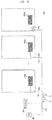
- FIG. 1 is a diagram illustrating an example of a photovoltaic system including a photovoltaic module according to an embodiment of the present invention.
- the photovoltaic system 10a may include a photovoltaic module 50 and a gateway 80.
- the photovoltaic module 50 may include a solar cell module 100, and a junction box 200 including a power converting device (500 in FIG. 6 ) which converts direct current (DC) power supplied from the solar cell module and outputs the converted DC power.
- a power converting device 500 in FIG. 6
- DC direct current
- the junction box 200 may be attached on a rear surface of the solar cell module 100, or may be spaced apart from the solar cell module 100 to be provided separately therefrom.
- a cable oln may be electrically connected to an output terminal of the junction box 200 to supply alternating current (AC) power, which is output from the junction box 200, to a grid.
- AC alternating current
- the gateway 80 may be interposed between the junction box 200 and the grid 90.
- the gateway 80 may detect an alternating current io and an alternating voltage vo which flow through the cable oln and are output from the photovoltaic module 50.
- the gateway 80 may output a power factor adjustment signal for adjusting a power factor based on a phase difference between the alternating current io and the alternating voltage vo which are output from the photovoltaic module 50.
- the gateway 80 and the photovoltaic module 50 may perform power line communication (PLC) by using a cable 323.
- PLC power line communication
- the power converting device (500 in FIG. 6 ) included in the photovoltaic module 50 may convert DC power, output from the solar cell module 100, into AC power, and may output the converted power.
- the power converting device (500 in FIG. 6 ) included in the photovoltaic module 50 may include a converter (530 in FIG. 6 ) and an inverter (540 in FIG. 6 ).
- a method of performing stable power output in the two-stage power converting device is provided. Particularly, even when DC power input from the solar cell module 100 is low, stable power output may be provided without limiting the range of output power.
- the photovoltaic module 50 may include the solar cell module 100, the converter 530, the inverter 540, and the controller 550.
- the converter 530 may include a full-bridge switching part 523, a transformer 536, and a half-bridge switching part 538.
- the controller 550 may change a switching frequency of the full-bridge switching part 523 and the half-bridge switching part 538 in a first section Pba and Pbb. In this manner, by changing the switching frequency of the full-bridge switching part 523 and the half-bridge switching part 538, stable power output may be provided.
- the controller 550 when changing the switching frequency of the full-bridge switching part 523 and the half-bridge switching part 538, the controller 550 may change a first phase difference between the full-bridge switching part 523 and the half-bridge switching part 538, thereby providing stable power output.
- the controller 550 may control driving of the full-bridge switching part 532 and the half-bridge switching part 538 by separating a section where the switching frequency of the full-bridge switching part 532 and the half-bridge switching part 538 is changed from a section where the switching frequency of the full-bridge switching part 532 and the half-bridge switching part 538 is constant, according to a waveform of an output voltage Vac of the inverter 540.
- FIG. 2 is a diagram illustrating another example of a photovoltaic system including a photovoltaic module according to an embodiment of the present invention.
- the photovoltaic system 10b may include a plurality of photovoltaic modules 50a, 50b, ..., and 50n and a gateway 80.
- the photovoltaic system 10b of FIG. 2 includes the plurality of photovoltaic modules 50a, 50b, ..., and 50n which are connected in parallel with each other.
- the plurality of photovoltaic modules 50a, 50b, ..., and 50n each include solar cell modules 100a, 100b, ..., and 100n; and junction boxes 200a, 200b, ..., and 200n including a circuit device which converts DC power input from the photovoltaic module and outputs the converted DC power.
- each of the junction boxes 200a, 200b, ..., and 200n is attached on a rear surface of each of the solar cell modules 100a, 100b, ..., and 100n, but is not limited thereto, and each of the junction boxes 200a, 200b, ..., and 200n may be spaced apart from each of the solar cell modules 100a, 100b, ..., and lOOn to be provided separately therefrom.
- Cables 31a, 31b, ..., and oln may be electrically connected to an output terminal of each of the junction boxes 200a, 200b, ..., and 200n to supply alternating current (AC) power, which is output from each of the junction boxes 200a, 200b, ..., and 200n, to a grid.
- AC alternating current
- the controller 550 of each of the plurality of photovoltaic modules 50a, 50b, ..., and 50n in FIG. 2 may change a switching frequency of the full-bridge switching part 523 and the half-bridge switching part 538 in the first section Pba and Pbb.
- the controller 550 of each of the plurality of photovoltaic modules 50a, 50b, ..., and 50n in FIG. 2 may change a first phase difference between the full-bridge switching part 523 and the half-bridge switching part 538.
- controller 550 of each of the plurality of photovoltaic modules 50a, 50b, ..., and 50n in FIG. 2 may control driving of the full-bridge switching part 532 and the half-bridge switching part 538 by separating a section where the switching frequency of the full-bridge switching part 532 and the half-bridge switching part 538 is changed from a section where the switching frequency of the full-bridge switching part 532 and the half-bridge switching part 538 is constant, according to a waveform of an output voltage Vac of the inverter 540.
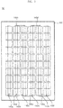
- FIG. 3 is a front view of a photovoltaic module according to an embodiment of the present invention.
- the photovoltaic module 50 may include a solar cell module 100, and a junction box 200 which is disposed on a rear surface of the solar cell module 100.
- the junction box 200 may include at least one bypass diode which may bypass DC power in order to prevent a hot spot when a shade phenomenon occurs.
- FIG. 4 and the following drawings illustrate the junction box 200 including three bypass diodes (Da, Db, Dc in FIG. 4 ) as opposed to four solar cell strings of FIG. 3 .
- the junction box 200 may convert DC power supplied from the solar cell module 100, which will be described with reference to FIG. 4 and the following drawings.
- the solar cell module 100 may include a plurality of solar cells.
- the plurality of solar cells are connected in series through a ribbon (133 in FIG. 12 ) to form a solar cell string 140.
- a ribbon 133 in FIG. 12
- six strings 140a, 140b, 140c, 140d, 140e, and 140f are formed, and each string includes 10 solar cells.
- various modifications may be made.
- Solar cell strings may be electrically connected with each other through a bus ribbon. As illustrated in FIG. 3 , a first solar cell string 140a and a second solar cell string 140b are electrically connected, a third solar cell string 140c and a fourth solar cell string 140d are electrically connected, and a fifth solar cell string 140e and a sixth solar cell string 140f are electrically connected, by the respective bus ribbons 145a, 145c, and 145e disposed at a lower portion of the solar cell 100.
- the second solar cell string 140b and the third solar cell string 140c are electrically connected, and the fourth solar cell string 140d and the fifth solar cell string 140e are electrically connected, by the respective bus ribbons 145b and 145d disposed at an upper portion of the solar cell 100.
- the ribbon connected to the first string, the bus ribbons 145b and 145d, and the ribbon connected to the fourth string are electrically connected to a first to a fourth conductive lines (not shown) respectively.
- the first to fourth conductive lines (not shown) may be connected to bypass diodes (Da, Db, and Dc in FIG. 4 ) in the junction box 200, which is disposed on a rear surface of the solar cell module 100, through an opening formed at the solar cell module 100.
- the opening formed at the solar cell module 100 may be formed at a position corresponding to a position where the junction box 200 is located.
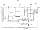
- FIG. 4 is a circuit diagram of a junction box in the photovoltaic module of FIG. 3 .
- the junction box 200 may convert DC power supplied from the solar cell module 100, and may output the converted power.
- the junction box 200 may include a power converting device for outputting AC power.
- the junction box 200 may include a converter 530, an inverter 540, and a controller 550 to control the same.
- junction box 200 may further include a bypass diode part 510 for bypassing, a capacitor part 520 for storing DC power, and a filter 570 for filtering output AC power.
- junction box 200 may further include a communicator 580 for communication with an external gateway 80.
- junction box 200 may further include an input current detector A, an input voltage detector B, a converter output current detector C, a converter output voltage detector D, an inverter output current detector E, and an inverter output voltage detector F.
- the controller 550 may control the converter 530, the inverter 540, and the communicator 580.
- the bypass diode 510 may include bypass diodes Dc, Db, and Da, each of which is disposed between the first to fourth conductive lines (not shown) of the solar cell module 100.
- the number of the bypass diodes is one or more, and is desired to be less by 1 than the number of conductive lines.
- the bypass diodes Dc, Db, and Da receive photovoltaic DC power from the solar cell module 100, particularly from the first to fourth conductive lines (not shown) of the solar cell module 100. Further, when a reverse voltage is generated from DC power supplied from at least one of the first to the fourth conductive lines (not shown), the bypass diodes Dc, Db, and Da may bypass the supplied DC power.
- the DC current may be input to the capacitor part 520.
- the capacitor part 520 may store the input DC current which is input after passing through the solar cell module 100 and the bypass diode part 510.
- the capacitor part 520 includes a plurality of capacitors Ca, Cb, and Cc which are connected in parallel. However, unlike the drawing, a plurality of capacitors may be connected in a combination of series and parallel connections, or may be connected in series to a ground terminal. Alternatively, the capacitor part 520 may include only one capacitor.
- the converter 530 may convert a level of voltage input from the solar cell module 100 after passing through the bypass diode 510 and the capacitor part 520.
- the converter 530 may perform power conversion by using the DC current stored in the capacitor part 520.
- the converter 530 according to an embodiment of the present invention will be described in further detail with reference to FIG. 6 .
- Switching elements in the converter 530 may be turned on/off based on a converter switching control signal from the controller 550. In this manner, a level-converted DC power may be output.
- the inverter 540 may convert the DC power, which is level-converted by the converter unit 530, into AC power.
- a full-bridge inverter in which upper arm switching elements Sa and Sb and lower arm switching elements S'a and S'b, which are connected in series with each other, form pairs such that a total of two pairs of upper and lower arm switching elements are connected in parallel (Sa & S'a and Sb & S'b) with each other.
- a diode may be connected in inverse parallel to each of the switching elements Sa, Sb, S'a, and S'b.
- the switching elements Sa, Sb, S'a, and S'b in the inverter 540 may be turned on and off based on an inverter switching control signal from the controller 550. In this manner, AC power having a predetermined frequency may be output, in which it is desired that AC power has the same frequency (about 60 Hz or 50 Hz) as an AC frequency of the grid.
- the capacitor C may be interposed between the converter 530 and the inverter 540.
- the capacitor C may store the level-converted DC power of the converter 530. Both ends of the capacitor C may be referred to as DC ends, and accordingly, the capacitor C may be referred to as a DC end capacitor.
- the input current detector A may detect the input current ic1 supplied from the solar cell module 100 to the capacitor part 520.
- the input voltage detector B may detect the input voltage vc1 supplied from the solar cell module 100 to the capacitor part 520.
- the input voltage vc1 may be the same as the voltage stored on both ends of the capacitor unit 520.
- the detected input current ic1 and input voltage vc1 may be input to the controller 550.
- the converter output current detector C detects an output current ic2, namely DC end current, which is output from the converter 530, and the converter output voltage detector D detects an output voltage vc2, namely DC end voltage, which is output from the converter 530.
- the detected output current i2 and output voltage vc2 may be input to the controller 550.
- An inverter output current detector E detects current ic3 output from the inverter 540, and an inverter output voltage detector E detects voltage vc3 output from the inverter 540.
- the detected output current ic3 and output voltage vc3 may be input to the controller 550.
- the controller 550 may output a control signal for controlling the switching elements of the converter 530. Particularly, the controller 550 may output a turn-on timing signal of the switching elements in the converter 530 based on at least one of the following: the detected input current ic1, input voltage vc1, output current ic2, output voltage vc2, output current ic3, and output voltage vc3.
- the controller 550 may output an inverter control signal for controlling the respective switching elements Sa, Sb, S'a, and S'b of the inverter 540. Particularly, the controller 550 may output a turn-on timing signal of the switching elements Sa, Sb, S'a, and S'b of the inverter 540 based on at least one of the following: the detected input current ic1, input voltage vc1, output current ic2, output voltage vc2, output current ic3, and output voltage vc3.
- controller 550 may calculate the maximum power point of the solar cell module 100, and accordingly may control the converter 530 to output DC power corresponding to the maximum power.
- the communicator 580 may perform communication with the gateway 80.
- the communicator 580 may exchange data with the gateway 80 through power line communication.
- the communicator 580 may transmit current information, voltage information, power information, and the like, of the photovoltaic module 50 to the gateway 80.
- the filter 570 may be disposed at an output terminal of the inverter 540.
- the filter 570 may include a plurality of passive devices, and may adjust a phase difference between the alternating current io and the alternating voltage vo, which are output from the inverter 540, based on at least some of the plurality of passive devices.
- FIGS. 5A and 5B are diagrams illustrating various examples of a power converting device of a photovoltaic module.
- a power converting device 600a of a photovoltaic module includes a capacitor part 620, a converter 630, an inverter 640, and a filter 670.
- the converter 630 of FIG. 5A includes an interleaved flyback converter, in which transformers T1a and T1b are used such that an input side is insulated from an output side, and a voltage conversion ratio is high, but it is difficult to control power factor (pf).
- a power converting device 600b of a photovoltaic module includes a capacitor part 620b, a power converter 640b, and a filter 670.
- the power converting device 640b further includes a diode Dbb and a switching element Sbb.
- power factor (pf) may be controlled, but the power converter 640b is of a non-insulated type, and has drawbacks in that a voltage conversion ratio is low, and a separate protection circuit is required to satisfy regulations regarding a leakage current. Further, the power converter 640b also has a drawback in that when switching, hard-switching causes hard-switching loss, leading to low power conversion efficiency.
- the present disclosure provides a method of providing stable power output by a two-stage power converting device, and a method of reducing loss of output power.
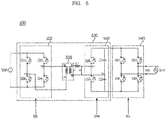
- FIG. 6 is a circuit diagram of a power converting device in a photovoltaic module according to an embodiment of the present invention
- FIGS. 7 to 12 are diagrams referred to in explaining the power converting device of FIG. 6 .
- the power converting device 500 in the photovoltaic module 50 may include a bypass diode part 510, a capacitor part 520, a controller 550, a communicator 580, an input current detector A, an input voltage detector B, a converter output current detector C, a converter output voltage detector D, an inverter output current detector E, and an inverter output voltage detector F, which are illustrated in FIG. 4 .
- a filter 570 for reducing an electromagnetic wave noise may be further included on an output terminal of the inverter 540, in which the filter 570 may include at least one inductor.
- the power converting device 500 in the photovoltaic module 50 includes: a solar cell module 100 having a plurality of solar cells 130; a converter 530 to convert a level of first direct current power Vin input from the solar cell module 100 to output second direct current power; an inverter 540 to convert the direct current power, supplied from the converter 530, into alternating current power Vac; and a controller 550 to control the converter 530 and the inverter 540.
- the converter 530 may include: a full-bridge switching part 532 to perform switching of the first DC power Vin; a transformer 536 having input sides na and nb connected to an output terminal of the full-bridge switching part 532; and a half-bridge switching part 538 connected to output sides nc and nd of the transformer 536.
- the controller 550 may change a switching frequency of the full-bridge switching part 532 and the half-bridge switching part 538 in a first section Pba and Pbb. In this manner, even in the case where DC power Vin input from the solar cell module 100 is low, stable power output may be provided without limiting the range of output power.
- switching loss may be reduced in the two-stage power converting device.
- the converter 530 in the power converting device 500 of the photovoltaic module 50 may further include an inductor Lr connected between the transformer 536 and the half-bridge switching part 538.
- the inductor Lr is required for energy transfer between the transformer 536 and the half-bridge switching part 538.
- the inductor Lr may be omitted, and leakage inductance of the transformer 536 may perform the function of the inductor Lr instead.
- the full-bridge switching part 532 may include a first switching element Q1 and a second switching element Q2 which are connected in parallel with each other, and a third switching element Q3 and a fourth switching element Q4 which are connected in series with the first switching element Q1 and the second switching element Q2 respectively.
- the input sides na and nb of the transformer 536 may be connected between a first node N1, which is between the first switching element Q1 and the second switching element Q2, and a second node N2 which is between the third switching element Q3 and the fourth switching element Q4.
- the half-bridge switching part 538 may include a fifth switching element Q5 and a sixth switching element Q6 which are connected in series with each other, and a first capacitor C1 and a second capacitor C2 which are connected in series with each other.
- the fifth switching element Q5 and the sixth switching element Q6, and the first capacitor C1 and the second capacitor C2 may be connected in parallel with each other.
- the output sides nc and nd of the transformer 536 may be connected between a third node Nd, which is between the fifth switching element Q5 and the sixth switching element Q6, and a fourth node N4 which is between the first capacitor C1 and the second capacitor C2.
- the controller 550 may output a switching control signal Sfb for switching the full-bridge switching part 532.
- controller 550 may output a switching control signal Shb for switching the half-bridge switching part 532.
- controller 550 may output a switching control signal Sic for switching the inverter 540.
- FIG. 7 is a diagram illustrating various waveforms in the power converting device 500.
- FIG. 7 (a) illustrates a waveform of a current Ilr passing through the inductor Lr.
- FIG. 7 illustrates a waveform of a switching control signal Ss1 applied to the switching element S1 in the full-bridge switching part 532.
- (c) illustrates a waveform of a switching control signal Ss4 applied to the switching element S4 in the half-bridge switching part 538.
- FIG. 7 illustrates a waveform of a switching control signal Ssa applied to a switching element Sa in the inverter 540.
- (e) illustrates a waveform of an output current lac which is output from the inverter 540.
- the second phase difference Dfb may be greater than the first phase difference Dfa.
- the controller 550 may change the switching frequency of the full-bridge switching part 532 and the half-bridge switching part 538 according to a waveform of the output voltage Vac of the inverter 540, which will be described with reference to FIG. 8 and the following drawings.
- FIG. 8 is a diagram illustrating a switching frequency of a full-bridge switching part 532 and a half-bridge switching part 538 according to a waveform of an output voltage Vac.
- of an output voltage waveform may have a frequency of 120 Hz which is approximately twice a system frequency of 60 Hz.
- the present disclosure provides a method of stably outputting a system voltage even in the case where a level of direct current power Vin produced by the solar cell module 100 is low.
- the switching frequency of the full-bridge switching part 532 and the half-bridge switching part 538 is changed based on an absolute value
- the present disclosure provides a method of changing the switching frequency of the full-bridge switching part 532 and the half-bridge switching part 538 for stable power output.
- the switching frequency increases; and as the switching frequency decreases, the output power increases, such that in the present disclosure, the switching frequency may be changed based on such feature.
- the switching frequency may be changed in reverse proportion to the absolute value
- a section Paa to a section Pab correspond to a period of the absolute value
- of the output voltage waveform is gradually increased; in the section Pc, the absolute value
- the sections Pba and Pbb may be referred to as a first section; the sections Paa and Pab may be referred to as a second section; and the section Pc may be referred to as a third section.
- the controller 550 may control driving of the full-bridge switching part 532 and the half-bridge switching part 538 by separating the sections Pba and Pbb where the switching frequency of the full-bridge switching part 532 and the half-bridge switching part 538 is changed from the sections Paa, Pc, and Pab where the switching frequency of the full-bridge switching part 532 and the half-bridge switching part 538 is constant, according to the waveform of the output voltage Vac of the inverter 540.
- the controller 550 may control the full-bridge switching part 532 and the half-bridge switching part 538 to be driven with a first switching frequency fa; and in the third section Pc, the controller 550 may control the full-bridge switching part 532 and the half-bridge switching part 538 to be driven with a second switching frequency fb which is lower than the first switching frequency fa.
- the first section Pba and Pbb may be interposed between the second section Paa and Pab and the third section Pc.
- the controller 550 may change the switching frequency of the full-bridge switching part 532 and the half-bridge switching part 538.
- the controller 550 may control the switching frequency of the full-bridge switching part 532 and the half-bridge switching part 538 to be decreased as illustrated in FIG. 8 .
- the controller 550 may control the switching frequency of the full-bridge switching part 532 and the half-bridge switching part 538 to be increased as illustrated in FIG. 8 .
- the switching frequency of the full-bridge switching part 532 and the half-bridge switching part 538 is changed such that the converter 530 may stably perform voltage level conversion.
- the controller 550 may control the switching frequency fc of the inverter 540 to be constant approximately at 120 Hz.
- the controller 550 may control the switching frequency of the full-bridge switching part 532 and the half-bridge switching part 538 to be changed in a range of 150 Hz to 40Khz.
- the switching frequency of the full-bridge switching part 532 and the half-bridge switching part 538 is greater than the switching frequency fc of the inverter 540.
- the controller 550 may control a second switching frequency fb to be decreased. In this case, as the switching frequency is lowered, power conversion may be more performed, thereby stably outputting a constant waveform of the output voltage.
- the controller 550 may control the third section Pc to be increased.
- a section of the switching frequency fb increases, such that output power may be increased.
- the controller 550 may change the first phase difference Dfa between the full-bridge switching part 532 and the half-bridge switching part 538 as illustrated in FIG. 7B .
- the controller 550 may change the second phase difference Dfb between the full-bridge switching part 532 and the inverter 540 as illustrated in FIG. 7B .
- FIGS. 9A to 9C are diagrams illustrating inductor current waveforms ILra, ILrb, and ILrc at points PA, PB, and PC of FIG. 8 .
- the point PA is a point in the third section Pc where the full-bridge switching part 532 and the half-bridge switching part 538 are driven with a minimum switching frequency fb.
- commutation current values Psta and Pstb of the full-bridge switching part 532 and the half-bridge switching part 538 may be higher than set values Seta and Setb.
- the point PB is a point in the first section Pbb where the switching frequency of the full-bridge switching part 532 and the half-bridge switching part 538 is changed.
- the commutation current value of the half-bridge switching part 538 is greater than the commutation current value of the full-bridge switching part 532.
- the point PC is a point in the first section Pbb where the switching frequency of the full-bridge switching part 532 and the half-bridge switching part 538 is changed.
- the commutation current value of the half-bridge switching part 538 is greater than the commutation current value of the full-bridge switching part 532.
- the commutation current value of the half-bridge switching part 538 of FIG. 9C may be smaller than the commutation current value of the half-bridge switching part 538 of FIG. 9B .
- the controller 550 may change the switching frequency of the full-bridge switching part 532 and the half-bridge switching part 538, and may control the shape of the waveform of the current flowing through the inductor Lr to be constant. In this case, a level of the current flowing through the inductor Lr may be lowered as the switching frequency is increased.
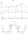
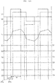
- FIG. 10A illustrates a voltage waveform V'1 on an output side of a transformer and a voltage waveform V2 on both ends of an inductor Lr, as well as a waveform of a current flowing through the inductor Lr.
- FIG. 10A also illustrates a waveform of a switching control signal applied to each of the switching elements Q1 to S6.
- g denotes a phase difference between the switching element Q4 and the switching element Q6; and w denotes a phase difference between the switching element Q6 and the switching element Q3.
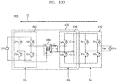
- Each waveform illustrated in FIG. 10A is in an active power mode, and is a waveform of a current flowing from the converter 530 to the inverter 540 as illustrated in FIG. 10B .
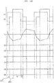
- FIG. 10C illustrates a voltage waveform V'1 on an output side of a transformer and a voltage waveform V2 on both ends of an inductor Lr, as well as a waveform of a current flowing through the inductor Lr.
- FIG. 10C also illustrates a waveform of a switching control signal applied to each of the switching elements Q1 to S6.
- w denotes a phase difference between the switching element Q4 and the switching element Q6; and g denotes a phase difference between the switching element Q5 and the switching element Q3.
- Each waveform illustrated in FIG. 10C is in a reactive power mode, and is a waveform of a current flowing from the inverter 540 to the converter 530 as illustrated in FIG. 10D .
- FIG. 11A illustrates a commutation current waveform of the full-bridge switching part 532; and FIG. 11B illustrates a commutation current waveform of the half-bridge switching part 538.
- the controller 550 may separate the commutation current of the full-bridge switching part 532 from the commutation current of the half-bridge switching part 538.
- the controller 550 may calculate a current value at each of points ⁇ 0, ⁇ 1, ⁇ 2, and ⁇ 3 by reference to the following Equations 1 to 4.
- V ac ⁇ w V sec 2 f s L ⁇ l ⁇ 1
- Vac denotes an output voltage
- fs denotes a switching frequency
- L ⁇ denotes inductance
- g and w denote a phase difference
- Vsec denotes an input voltage Vin.
- I ⁇ 1 _Com and I ⁇ 2_ Com may denote a switch communication current at points T1 and T2 respectively.
- each switching element of the full-bridge switching part 532 and the half-bridge switching part 538 satisfies requirements of the following Equation 5.
- FIG. 12 is a diagram illustrating a relationship between an input voltage, an output voltage and a switching frequency.
- FIG. 12 (a) illustrates an example where a switching frequency Fsw of the full-bridge switching part 532 and the half-bridge switching part 538 is changed in proportion to the input voltage Vin.
- the controller 550 may change the switching frequency Fsw of the full-bridge switching part 532 and the half-bridge switching part 538 in proportion to the input voltage Vin.
- FIG. 12 illustrates an example where the switching frequency Fsw of the full-bridge switching part 532 and the half-bridge switching part 538 is changed in reverse proportion to the output voltage Vac.
- the controller 550 may change the switching frequency Fsw of the full-bridge switching part 532 and the half-bridge switching part 538 in reverse proportion to the output voltage Vac.
- the controller 550 may change the switching frequency of the full-bridge switching part 532 and the half-bridge switching part 538 in the first section Pba and Pbb, thereby enabling stable power output.
- a turn ratio of the transformer 536 may be reduced, and the size of the transformer 536 may also be reduced, thereby reducing the size of the junction box 200 including the converter 530 and the like.
- the controller 550 lowers the second switching frequency fb, such that even when DC power input from the solar cell module 100 is low, stable power output may be provided without limiting the range of output power.
- the controller 550 controls the third section Pc to be increased to perform power conversion, thereby enabling stable output of AC power.
- the controller 550 may change the switching frequency of the full-bridge switching part 532 and the half-bridge switching part 538, thereby enabling stable output of AC power.
- controller 550 may perform two-stage power conversion by using the converter 530 and the inverter 540, thereby improving power factor.
- the controller 550 may change the first phase difference between the full-bridge switching part 532 and the half-bridge switching part 538, thereby providing stable power output.
- the controller 550 may control driving of the full-bridge switching part 532 and the half-bridge switching part 538 by separating a section where the switching frequency of the full-bridge switching part 532 and the half-bridge switching part 538 is changed from a section where the switching frequency of the full-bridge switching part 532 and the half-bridge switching part 538 is constant, according to a waveform of the output voltage Vac of the inverter 540, thereby providing stable power output.
- FIG. 13 is an exploded perspective view of a solar cell module of FIG. 3 .
- the solar cell module 100 includes a plurality of solar cells 130.
- the solar cell module 100 may further include a first sealing material 120 and a second sealing material 150 which are disposed at a lower surface and an upper surface of each of the solar cells 130; a rear substrate 110 disposed at a lower surface of the first sealing material 120; and a front substrate 160 disposed at an upper surface of the second sealing material 150.
- Each of the solar cells 130 is a semiconductor device to convert solar energy into electrical energy, and examples thereof include a silicon solar cell, a compound semiconductor solar cell, a tandem solar cell, a dye-sensitized solar cell, a CdTe solar cell, a CIGS solar cell, a thin-film solar cell, and the like.
- Each of the solar cells 130 has a light receiving surface, on which sunlight is incident, and a back surface which is opposite the light receiving surface.
- the solar cell 130 includes: a first conductive type silicon substrate; a second conductive type semiconductor layer formed on the silicon substrate, the second conductive type being opposite to the first conductive type; at least one or more openings through which a portion of the second conductive type semiconductor layer is exposed; an anti-reflection film formed on the second conductive type semiconductor layer; a front electrode which contacts the portion of the second conductive type semiconductor layer exposed through the at least one or more openings; and a rear electrode formed at the rear surface of the silicon substrate.
- Each of the solar cells 130 may be electrically connected in series or in parallel, or may be connected in a serial-parallel manner. Specifically, the plurality of solar cells 130 may be electrically connected to each other via ribbons 133. Each of the ribbons 133 may be bonded to the front electrode formed on the light receiving surface of one of the solar cells 130 and the rear electrode formed on the back surface of another adjacent one of the solar cells.
- the ribbons 133 are arranged in two rows and the plurality of solar cells 130 are connected in series by the ribbons 133 to form one solar cell string 140.
- the rear substrate 110 is a back sheet having waterproof, insulation, and ultraviolet protection functions, and may be a Tedlar/PET/Tedlar (TPT) type substrate, but is not limited thereto.
- FIG. 4 illustrates an example where the rear substrate 110 is formed in a rectangular shape, but the rear substrate 110 is not limited thereto, and may be formed in various shapes, such as a circular shape and a semi-circular shape, depending on the environment where the solar cell module 100 is installed.
- the first sealing material 120 may be attached to the rear substrate 110, with the size of the first sealing material 120 being the same as the size of the rear substrate 110, and the plurality of solar cells 130 may be arranged on the first sealing material 120, with the solar cells 130 being adjacent to each other to form several strings.
- the second sealing material 150 which is disposed on the solar cell 130, may be bonded to the first sealing material 120 by lamination
- first sealing material 120 and the second sealing material 150 enable elements of the solar cell to be chemically combined, and examples thereof include Ethylene Vinyl Acetate (EVA) film, and the like.
- EVA Ethylene Vinyl Acetate
- the front substrate 160 may be disposed on the second sealing material 150 for sunlight transmission, and it is desired that the front substrate 160 is made of reinforced glass to protect the solar cells 130 from external impact and the like. Further, it is further desired that the front substrate 160 is made of low-iron reinforced glass to prevent reflection of sunlight and to increase transmittance of sunlight.
- a photovoltaic module including: a solar cell module including a plurality of solar cells; a converter to convert a level of first direct current (DC) power input from the solar cell module, and to output second DC power; an inverter to convert the DC power supplied from the converter into alternating current (AC) power; and a controller to control the converter and the inverter, wherein the converter includes: a full-bridge switching part to switch the first DC power; a transformer having an input side connected to an output terminal of the full-bridge switching part; and a half-bridge switching part connected to an output side of the transformer, wherein the controller changes a switching frequency of the full-bridge switching part and the half-bridge switching part in a first section, thereby enabling stable power output.
- DC direct current
- AC alternating current
- a turn ratio of the transformer may be reduced, and the size of the transformer may also be reduced, thereby reducing the size of the junction box including the converter and the like.
- the controller may lower the second switching frequency, such that even when DC power input from the solar cell module is low, stable power output may be provided without limiting the range of output power.
- the controller may control a third section to be increased to perform power conversion, thereby enabling stable output of AC power.
- the controller may change the switching frequency of the full-bridge switching part and the half-bridge switching part according to a waveform of an output voltage of the inverter, thereby enabling stable output of AC power.
- controller may perform two-stage power conversion by using the converter and the inverter, thereby improving power factor.
- a photovoltaic module including: a solar cell module including a plurality of solar cells; a converter to convert a level of first direct current (DC) power input from the solar cell module, and to output second DC power; an inverter to convert the DC power supplied from the converter into alternating current (AC) power; and a controller to control the converter and the inverter, wherein the converter includes: a full-bridge switching part to switch the first DC power; a transformer having an input side connected to an output terminal of the full-bridge switching part; and a half-bridge switching part connected to an output side of the transformer, wherein when changing a switching frequency of the full-bridge switching part and the half-bridge switching part, the controller changes a first phase difference between the full-bridge switching part and the half-bridge switching part, thereby enabling stable power output.
- DC direct current
- AC alternating current
- a photovoltaic module including: a solar cell module including a plurality of solar cells; a converter to convert a level of first direct current (DC) power input from the solar cell module, and to output second DC power; an inverter to convert the DC power supplied from the converter into alternating current (AC) power; and a controller to control the converter and the inverter, wherein the converter includes: a full-bridge switching part to switch the first DC power; a transformer having an input side connected to an output terminal of the full-bridge switching part; and a half-bridge switching part connected to an output side of the transformer, wherein the controller controls driving of the full-bridge switching part and the half-bridge switching part by separating a section where a switching frequency of the full-bridge switching part and the half-bridge switching part is changed from a section where the switching frequency of the full-bridge switching part and the half-bridge switching part is constant, according to a waveform of an output voltage of the inverter, thereby enabling stable power
- the photovoltaic module is not limited to the configuration and method of the above-described embodiments, and all or some of the above embodiments may be selectively combined with each other to enable various modifications thereof.
Landscapes
- Engineering & Computer Science (AREA)
- Power Engineering (AREA)
- Inverter Devices (AREA)
- Photovoltaic Devices (AREA)
- Dc-Dc Converters (AREA)
Abstract
Description
- This application claims the priority benefit of Korean Patent Application No.
10-2017-0122785, filed on September 22, 2017 - The present disclosure relates to a photovoltaic module, and more particularly, to a photovoltaic module which may provide stable power output.
- Recently, as existing energy resources, such as oil and coal, are predicted to be depleted, there has been an increasing interest in alternative energy resources to replace the existing energy. Among the alternative energy resources, solar cells, which directly convert solar energy into electrical energy by using a semiconductor device, receive attention as a next-generation cell.
- The photovoltaic module refers to a device in which solar cells for solar energy generation are connected in series or in parallel.
- In the case where the photovoltaic module outputs alternating current (AC) power to a grid by using a converter and an inverter, if electricity produced by the solar cells is low, power is low even after power conversion. Accordingly, research continues to develop a photovoltaic module which may provide stable power output.
- It is an object of the present invention to provide a photovoltaic module which may provide stable power output.
- It is another object of the present invention to provide a photovoltaic module which may reduce the size of a transformer in the photovoltaic module.
- In accordance with an aspect of the present invention, the above and other objects can be accomplished by the provision of a photovoltaic module including: a solar cell module including a plurality of solar cells; a converter to convert a level of first direct current (DC) power input from the solar cell module, and to output second DC power; an inverter to convert the DC power supplied from the converter into alternating current (AC) power; and a controller to control the converter and the inverter, wherein the converter includes: a full-bridge switching part to switch the first DC power; a transformer having an input side connected to an output terminal of the full-bridge switching part; and a half-bridge switching part connected to an output side of the transformer, wherein the controller changes a switching frequency of the full-bridge switching part and the half-bridge switching part in a first section.
-
-
FIG. 1 is a diagram illustrating an example of a photovoltaic system including a photovoltaic module according to an embodiment of the present invention. -
FIG. 2 is a diagram illustrating another example of a photovoltaic system including a photovoltaic module according to an embodiment of the present invention. -
FIG. 3 is a front view of a photovoltaic module according to an embodiment of the present invention. -
FIG. 4 is a circuit diagram of a junction box in the photovoltaic module ofFIG. 3 . -
FIGS. 5A and 5B are diagrams illustrating various examples of a power converting device of a photovoltaic module. -
FIG. 6 is a circuit diagram of a power converting device in a photovoltaic module according to an embodiment of the present invention. -
FIGS. 7 to 12 are diagrams referred to in explaining the power converting device ofFIG. 6 . -
FIG. 13 is an exploded perspective view of a solar cell module ofFIG. 3 . - In the present disclosure, as a method of reducing loss of output power which is output from a photovoltaic module, there is provided a method of controlling a power factor which is a phase difference between an alternating current and an alternating voltage which are output from the photovoltaic module.
- Hereinafter, embodiments of the present disclosure will be described in detail with reference to the accompanying drawings.
- In the following description, the terms "module" and "unit", which are used herein to signify components, are merely intended to facilitate explanation of the present disclosure, and the terms do not have any distinguishable difference in meaning or role. Thus, the terms "module" and "unit" may be used interchangeably.
-
FIG. 1 is a diagram illustrating an example of a photovoltaic system including a photovoltaic module according to an embodiment of the present invention. - Referring to
FIG. 1 , thephotovoltaic system 10a may include aphotovoltaic module 50 and agateway 80. - The
photovoltaic module 50 may include asolar cell module 100, and ajunction box 200 including a power converting device (500 inFIG. 6 ) which converts direct current (DC) power supplied from the solar cell module and outputs the converted DC power. - The
junction box 200 may be attached on a rear surface of thesolar cell module 100, or may be spaced apart from thesolar cell module 100 to be provided separately therefrom. - A cable oln may be electrically connected to an output terminal of the
junction box 200 to supply alternating current (AC) power, which is output from thejunction box 200, to a grid. - The
gateway 80 may be interposed between thejunction box 200 and thegrid 90. - Further, the
gateway 80 may detect an alternating current io and an alternating voltage vo which flow through the cable oln and are output from thephotovoltaic module 50. - In addition, the
gateway 80 may output a power factor adjustment signal for adjusting a power factor based on a phase difference between the alternating current io and the alternating voltage vo which are output from thephotovoltaic module 50. - To this end, the
gateway 80 and thephotovoltaic module 50 may perform power line communication (PLC) by using acable 323. - The power converting device (500 in
FIG. 6 ) included in thephotovoltaic module 50 may convert DC power, output from thesolar cell module 100, into AC power, and may output the converted power. - To this end, the power converting device (500 in
FIG. 6 ) included in thephotovoltaic module 50 may include a converter (530 inFIG. 6 ) and an inverter (540 inFIG. 6 ). - In the present disclosure, description is made based on a two-stage power converting device, in which the
converter 530 included in the power converting device (500 inFIG. 6 ) converts a level of DC power supplied from thesolar cell module 100, and then theinverter 540 converts the AC power. - Further, in the present disclosure, there is provided a method of performing stable power output in the two-stage power converting device. Particularly, even when DC power input from the
solar cell module 100 is low, stable power output may be provided without limiting the range of output power. - To this end, the
photovoltaic module 50 according to an embodiment of the present invention may include thesolar cell module 100, theconverter 530, theinverter 540, and thecontroller 550. - Particularly, the
converter 530 may include a full-bridge switching part 523, atransformer 536, and a half-bridge switching part 538. - In one embodiment of the present invention, the
controller 550 may change a switching frequency of the full-bridge switching part 523 and the half-bridge switchingpart 538 in a first section Pba and Pbb. In this manner, by changing the switching frequency of the full-bridge switching part 523 and the half-bridge switchingpart 538, stable power output may be provided. - In another embodiment of the present invention, when changing the switching frequency of the full-bridge switching part 523 and the half-bridge switching
part 538, thecontroller 550 may change a first phase difference between the full-bridge switching part 523 and the half-bridge switchingpart 538, thereby providing stable power output. - Further, in yet another embodiment of the present invention, the
controller 550 may control driving of the full-bridge switchingpart 532 and the half-bridge switchingpart 538 by separating a section where the switching frequency of the full-bridge switchingpart 532 and the half-bridge switching part 538 is changed from a section where the switching frequency of the full-bridge switchingpart 532 and the half-bridge switchingpart 538 is constant, according to a waveform of an output voltage Vac of theinverter 540. -
FIG. 2 is a diagram illustrating another example of a photovoltaic system including a photovoltaic module according to an embodiment of the present invention. - Referring to
FIG. 2 , thephotovoltaic system 10b may include a plurality ofphotovoltaic modules gateway 80. - Unlike the
photovoltaic system 10a ofFIG. 1 , thephotovoltaic system 10b ofFIG. 2 includes the plurality ofphotovoltaic modules - The plurality of
photovoltaic modules junction boxes - In
FIG. 2 , each of thejunction boxes junction boxes -
Cables junction boxes junction boxes - The
controller 550 of each of the plurality ofphotovoltaic modules FIG. 2 may change a switching frequency of the full-bridge switching part 523 and the half-bridge switchingpart 538 in the first section Pba and Pbb. - Further, when changing the switching frequency of the full-bridge switching part 523 and the half-bridge switching
part 538, thecontroller 550 of each of the plurality ofphotovoltaic modules FIG. 2 may change a first phase difference between the full-bridge switching part 523 and the half-bridge switchingpart 538. - In addition, the
controller 550 of each of the plurality ofphotovoltaic modules FIG. 2 may control driving of the full-bridge switchingpart 532 and the half-bridge switchingpart 538 by separating a section where the switching frequency of the full-bridge switchingpart 532 and the half-bridge switchingpart 538 is changed from a section where the switching frequency of the full-bridge switchingpart 532 and the half-bridge switchingpart 538 is constant, according to a waveform of an output voltage Vac of theinverter 540. -
FIG. 3 is a front view of a photovoltaic module according to an embodiment of the present invention. - Referring to
FIG. 3 , thephotovoltaic module 50 according to an embodiment of the present invention may include asolar cell module 100, and ajunction box 200 which is disposed on a rear surface of thesolar cell module 100. - The
junction box 200 may include at least one bypass diode which may bypass DC power in order to prevent a hot spot when a shade phenomenon occurs. -
FIG. 4 and the following drawings illustrate thejunction box 200 including three bypass diodes (Da, Db, Dc inFIG. 4 ) as opposed to four solar cell strings ofFIG. 3 . - The
junction box 200 may convert DC power supplied from thesolar cell module 100, which will be described with reference toFIG. 4 and the following drawings. - The
solar cell module 100 may include a plurality of solar cells. - In the drawings, the plurality of solar cells are connected in series through a ribbon (133 in
FIG. 12 ) to form asolar cell string 140. In this manner, sixstrings - Solar cell strings may be electrically connected with each other through a bus ribbon. As illustrated in
FIG. 3 , a firstsolar cell string 140a and a secondsolar cell string 140b are electrically connected, a thirdsolar cell string 140c and a fourthsolar cell string 140d are electrically connected, and a fifthsolar cell string 140e and a sixthsolar cell string 140f are electrically connected, by therespective bus ribbons solar cell 100. - Further, as illustrated in
FIG. 3 , the secondsolar cell string 140b and the thirdsolar cell string 140c are electrically connected, and the fourthsolar cell string 140d and the fifthsolar cell string 140e are electrically connected, by therespective bus ribbons solar cell 100. - The ribbon connected to the first string, the
bus ribbons FIG. 4 ) in thejunction box 200, which is disposed on a rear surface of thesolar cell module 100, through an opening formed at thesolar cell module 100. - In this case, the opening formed at the
solar cell module 100 may be formed at a position corresponding to a position where thejunction box 200 is located. -
FIG. 4 is a circuit diagram of a junction box in the photovoltaic module ofFIG. 3 . - Referring to
FIG. 4 , thejunction box 200 may convert DC power supplied from thesolar cell module 100, and may output the converted power. - Particularly, in the present disclosure, the
junction box 200 may include a power converting device for outputting AC power. - To this end, the
junction box 200 may include aconverter 530, aninverter 540, and acontroller 550 to control the same. - Further, the
junction box 200 may further include abypass diode part 510 for bypassing, acapacitor part 520 for storing DC power, and a filter 570 for filtering output AC power. - In addition, the
junction box 200 may further include acommunicator 580 for communication with anexternal gateway 80. - Moreover, the
junction box 200 may further include an input current detector A, an input voltage detector B, a converter output current detector C, a converter output voltage detector D, an inverter output current detector E, and an inverter output voltage detector F. - The
controller 550 may control theconverter 530, theinverter 540, and thecommunicator 580. - The
bypass diode 510 may include bypass diodes Dc, Db, and Da, each of which is disposed between the first to fourth conductive lines (not shown) of thesolar cell module 100. In this case, the number of the bypass diodes is one or more, and is desired to be less by 1 than the number of conductive lines. - The bypass diodes Dc, Db, and Da receive photovoltaic DC power from the
solar cell module 100, particularly from the first to fourth conductive lines (not shown) of thesolar cell module 100. Further, when a reverse voltage is generated from DC power supplied from at least one of the first to the fourth conductive lines (not shown), the bypass diodes Dc, Db, and Da may bypass the supplied DC power. - After passing through the
bypass diode part 510, the DC current may be input to thecapacitor part 520. - The
capacitor part 520 may store the input DC current which is input after passing through thesolar cell module 100 and thebypass diode part 510. - In the drawing, the
capacitor part 520 includes a plurality of capacitors Ca, Cb, and Cc which are connected in parallel. However, unlike the drawing, a plurality of capacitors may be connected in a combination of series and parallel connections, or may be connected in series to a ground terminal. Alternatively, thecapacitor part 520 may include only one capacitor. - The
converter 530 may convert a level of voltage input from thesolar cell module 100 after passing through thebypass diode 510 and thecapacitor part 520. - Particularly, the
converter 530 may perform power conversion by using the DC current stored in thecapacitor part 520. - The
converter 530 according to an embodiment of the present invention will be described in further detail with reference toFIG. 6 . - Switching elements in the
converter 530 may be turned on/off based on a converter switching control signal from thecontroller 550. In this manner, a level-converted DC power may be output. - The
inverter 540 may convert the DC power, which is level-converted by theconverter unit 530, into AC power. - In the drawing, a full-bridge inverter is illustrated, in which upper arm switching elements Sa and Sb and lower arm switching elements S'a and S'b, which are connected in series with each other, form pairs such that a total of two pairs of upper and lower arm switching elements are connected in parallel (Sa & S'a and Sb & S'b) with each other. A diode may be connected in inverse parallel to each of the switching elements Sa, Sb, S'a, and S'b.
- The switching elements Sa, Sb, S'a, and S'b in the
inverter 540 may be turned on and off based on an inverter switching control signal from thecontroller 550. In this manner, AC power having a predetermined frequency may be output, in which it is desired that AC power has the same frequency (about 60 Hz or 50 Hz) as an AC frequency of the grid. - The capacitor C may be interposed between the
converter 530 and theinverter 540. - The capacitor C may store the level-converted DC power of the
converter 530. Both ends of the capacitor C may be referred to as DC ends, and accordingly, the capacitor C may be referred to as a DC end capacitor. - The input current detector A may detect the input current ic1 supplied from the
solar cell module 100 to thecapacitor part 520. - The input voltage detector B may detect the input voltage vc1 supplied from the
solar cell module 100 to thecapacitor part 520. Here, the input voltage vc1 may be the same as the voltage stored on both ends of thecapacitor unit 520. - The detected input current ic1 and input voltage vc1 may be input to the
controller 550. - The converter output current detector C detects an output current ic2, namely DC end current, which is output from the
converter 530, and the converter output voltage detector D detects an output voltage vc2, namely DC end voltage, which is output from theconverter 530. The detected output current i2 and output voltage vc2 may be input to thecontroller 550. - An inverter output current detector E detects current ic3 output from the
inverter 540, and an inverter output voltage detector E detects voltage vc3 output from theinverter 540. The detected output current ic3 and output voltage vc3 may be input to thecontroller 550. - The
controller 550 may output a control signal for controlling the switching elements of theconverter 530. Particularly, thecontroller 550 may output a turn-on timing signal of the switching elements in theconverter 530 based on at least one of the following: the detected input current ic1, input voltage vc1, output current ic2, output voltage vc2, output current ic3, and output voltage vc3. - Further, the
controller 550 may output an inverter control signal for controlling the respective switching elements Sa, Sb, S'a, and S'b of theinverter 540. Particularly, thecontroller 550 may output a turn-on timing signal of the switching elements Sa, Sb, S'a, and S'b of theinverter 540 based on at least one of the following: the detected input current ic1, input voltage vc1, output current ic2, output voltage vc2, output current ic3, and output voltage vc3. - In addition, the
controller 550 may calculate the maximum power point of thesolar cell module 100, and accordingly may control theconverter 530 to output DC power corresponding to the maximum power. - The
communicator 580 may perform communication with thegateway 80. - For example, the
communicator 580 may exchange data with thegateway 80 through power line communication. - Further, the
communicator 580 may transmit current information, voltage information, power information, and the like, of thephotovoltaic module 50 to thegateway 80. - In addition, the filter 570 may be disposed at an output terminal of the
inverter 540. - The filter 570 may include a plurality of passive devices, and may adjust a phase difference between the alternating current io and the alternating voltage vo, which are output from the
inverter 540, based on at least some of the plurality of passive devices. -
FIGS. 5A and 5B are diagrams illustrating various examples of a power converting device of a photovoltaic module. - In
FIG. 5A , apower converting device 600a of a photovoltaic module includes acapacitor part 620, aconverter 630, aninverter 640, and afilter 670. - The
converter 630 ofFIG. 5A includes an interleaved flyback converter, in which transformers T1a and T1b are used such that an input side is insulated from an output side, and a voltage conversion ratio is high, but it is difficult to control power factor (pf). - In
FIG. 5B , apower converting device 600b of a photovoltaic module includes acapacitor part 620b, apower converter 640b, and afilter 670. - In addition to switching elements S1b to S4b related to the full-bridge inverter, the
power converting device 640b further includes a diode Dbb and a switching element Sbb. - In the
power converter 640b ofFIG. 5B , power factor (pf) may be controlled, but thepower converter 640b is of a non-insulated type, and has drawbacks in that a voltage conversion ratio is low, and a separate protection circuit is required to satisfy regulations regarding a leakage current. Further, thepower converter 640b also has a drawback in that when switching, hard-switching causes hard-switching loss, leading to low power conversion efficiency. - The present disclosure provides a method of providing stable power output by a two-stage power converting device, and a method of reducing loss of output power.
-
FIG. 6 is a circuit diagram of a power converting device in a photovoltaic module according to an embodiment of the present invention; andFIGS. 7 to 12 are diagrams referred to in explaining the power converting device ofFIG. 6 . - Referring to the drawings, in addition to a
converter 530 and aninverter 540 illustrated therein, thepower converting device 500 in thephotovoltaic module 50 may include abypass diode part 510, acapacitor part 520, acontroller 550, acommunicator 580, an input current detector A, an input voltage detector B, a converter output current detector C, a converter output voltage detector D, an inverter output current detector E, and an inverter output voltage detector F, which are illustrated inFIG. 4 . - Moreover, a filter 570 for reducing an electromagnetic wave noise may be further included on an output terminal of the
inverter 540, in which the filter 570 may include at least one inductor. - Hereinafter, description will be made based on the
converter 530, theinverter 540, and the like illustrated inFIG. 6 . - The
power converting device 500 in thephotovoltaic module 50 according to an embodiment of the present invention includes: asolar cell module 100 having a plurality ofsolar cells 130; aconverter 530 to convert a level of first direct current power Vin input from thesolar cell module 100 to output second direct current power; aninverter 540 to convert the direct current power, supplied from theconverter 530, into alternating current power Vac; and acontroller 550 to control theconverter 530 and theinverter 540. - The
converter 530 according to an embodiment of the present invention may include: a full-bridge switching part 532 to perform switching of the first DC power Vin; atransformer 536 having input sides na and nb connected to an output terminal of the full-bridge switching part 532; and a half-bridge switching part 538 connected to output sides nc and nd of thetransformer 536. - The
controller 550 may change a switching frequency of the full-bridge switching part 532 and the half-bridge switching part 538 in a first section Pba and Pbb. In this manner, even in the case where DC power Vin input from thesolar cell module 100 is low, stable power output may be provided without limiting the range of output power. - Further, switching loss may be reduced in the two-stage power converting device.
- The
converter 530 in thepower converting device 500 of thephotovoltaic module 50 may further include an inductor Lr connected between thetransformer 536 and the half-bridge switching part 538. - In this case, the inductor Lr is required for energy transfer between the
transformer 536 and the half-bridge switching part 538. - The inductor Lr may be omitted, and leakage inductance of the
transformer 536 may perform the function of the inductor Lr instead. - As illustrated in the drawings, the full-
bridge switching part 532 may include a first switching element Q1 and a second switching element Q2 which are connected in parallel with each other, and a third switching element Q3 and a fourth switching element Q4 which are connected in series with the first switching element Q1 and the second switching element Q2 respectively. - Further, the input sides na and nb of the
transformer 536 may be connected between a first node N1, which is between the first switching element Q1 and the second switching element Q2, and a second node N2 which is between the third switching element Q3 and the fourth switching element Q4. - As illustrated in the drawings, the half-
bridge switching part 538 may include a fifth switching element Q5 and a sixth switching element Q6 which are connected in series with each other, and a first capacitor C1 and a second capacitor C2 which are connected in series with each other. - In this case, the fifth switching element Q5 and the sixth switching element Q6, and the first capacitor C1 and the second capacitor C2, may be connected in parallel with each other.
- Further, the output sides nc and nd of the
transformer 536 may be connected between a third node Nd, which is between the fifth switching element Q5 and the sixth switching element Q6, and a fourth node N4 which is between the first capacitor C1 and the second capacitor C2. - The
controller 550 may output a switching control signal Sfb for switching the full-bridge switching part 532. - Further, the
controller 550 may output a switching control signal Shb for switching the half-bridge switching part 532. - In addition, the
controller 550 may output a switching control signal Sic for switching theinverter 540. -
FIG. 7 is a diagram illustrating various waveforms in thepower converting device 500. - In
FIG. 7, (a) illustrates a waveform of a current Ilr passing through the inductor Lr. - In
FIG. 7, (b) illustrates a waveform of a switching control signal Ss1 applied to the switching element S1 in the full-bridge switching part 532. - In
FIG. 7, (c) illustrates a waveform of a switching control signal Ss4 applied to the switching element S4 in the half-bridge switching part 538. - In
FIG. 7, (d) illustrates a waveform of a switching control signal Ssa applied to a switching element Sa in theinverter 540. - In
FIG. 7, (e) illustrates a waveform of an output current lac which is output from theinverter 540. - Upon comparing the switching control signal Ss1 of the full-
bridge switching part 532 with the switching control signal Ss4 of the half-bridge switching part 538, it can be seen that a first phase difference Dfa occurs between the full-bridge switching part 532 and the half-bridge switching part 538. - That is, there is the first phase difference Dfa between the switching control signal Ss1 of the full-
bridge switching part 532 and the switching control signal Ss4 of the half-bridge switching part 538. - Then, upon comparing the switching control signal Ss1 of the of the full-
bridge switching part 532 and the switching control signal Ssa of theinverter 540, a second phase difference Dfb occurs between the full-bridge switching part 532 and theinverter 540. - That is, there is the second phase difference Dfb between the switching control signal Ss1 of the full-
bridge switching part 532 and the switching control signal Ssa of theinverter 540. - In this case, the second phase difference Dfb may be greater than the first phase difference Dfa.
- The
controller 550 may change the switching frequency of the full-bridge switching part 532 and the half-bridge switching part 538 according to a waveform of the output voltage Vac of theinverter 540, which will be described with reference toFIG. 8 and the following drawings. -
FIG. 8 is a diagram illustrating a switching frequency of a full-bridge switching part 532 and a half-bridge switching part 538 according to a waveform of an output voltage Vac. - Referring to
FIG. 8 , an absolute value |Vac| of an output voltage waveform may have a frequency of 120 Hz which is approximately twice a system frequency of 60 Hz. - The present disclosure provides a method of stably outputting a system voltage even in the case where a level of direct current power Vin produced by the
solar cell module 100 is low. - To this end, in the present disclosure, the switching frequency of the full-
bridge switching part 532 and the half-bridge switching part 538 is changed based on an absolute value |Vin| of the input voltage Vin or the absolute value |Vac| of the output voltage waveform. - If the switching frequency of the full-
bridge switching part 532 and the half-bridge switching part 538 is constant, power output is limited, such that the present disclosure provides a method of changing the switching frequency of the full-bridge switching part 532 and the half-bridge switching part 538 for stable power output. - As the switching frequency increases, the output power decreases; and as the switching frequency decreases, the output power increases, such that in the present disclosure, the switching frequency may be changed based on such feature.
- For example, as illustrated in
FIG. 8 , the switching frequency may be changed in reverse proportion to the absolute value |Vin| of the input voltage Vin or the absolute value |Vac| of the output voltage waveform. - In
FIG. 8 , a section Paa to a section Pab correspond to a period of the absolute value |Vac| of the output voltage waveform. - Specifically, in
FIG. 8 , in the sections Paa and Pba, the absolute value |Vac| of the output voltage waveform is gradually increased; in the section Pc, the absolute value |Vac| of the output voltage waveform has a peak value; and in the sections Pbb and Pab, the absolute value |Vac| of the output voltage waveform is decreased. - The sections Pba and Pbb may be referred to as a first section; the sections Paa and Pab may be referred to as a second section; and the section Pc may be referred to as a third section.
- The
controller 550 may control driving of the full-bridge switching part 532 and the half-bridge switching part 538 by separating the sections Pba and Pbb where the switching frequency of the full-bridge switching part 532 and the half-bridge switching part 538 is changed from the sections Paa, Pc, and Pab where the switching frequency of the full-bridge switching part 532 and the half-bridge switching part 538 is constant, according to the waveform of the output voltage Vac of theinverter 540. - Particularly, in the second section Paa and Pab, the
controller 550 may control the full-bridge switching part 532 and the half-bridge switching part 538 to be driven with a first switching frequency fa; and in the third section Pc, thecontroller 550 may control the full-bridge switching part 532 and the half-bridge switching part 538 to be driven with a second switching frequency fb which is lower than the first switching frequency fa. - The first section Pba and Pbb may be interposed between the second section Paa and Pab and the third section Pc.
- In the first section Pba and Pbb, the
controller 550 may change the switching frequency of the full-bridge switching part 532 and the half-bridge switching part 538. - Particularly, in the section Pba which is a section at a transition from the second section Paa to the third section Pc, the
controller 550 may control the switching frequency of the full-bridge switching part 532 and the half-bridge switching part 538 to be decreased as illustrated inFIG. 8 . - Further, in the section Pbb which is a section at a transition from the third section Pc to the second section Paa and Pab, the
controller 550 may control the switching frequency of the full-bridge switching part 532 and the half-bridge switching part 538 to be increased as illustrated inFIG. 8 . - As described above, in some sections of the output voltage waveform, the switching frequency of the full-
bridge switching part 532 and the half-bridge switching part 538 is changed such that theconverter 530 may stably perform voltage level conversion. - In the first section Pba and Pbb, the
controller 550 may control the switching frequency fc of theinverter 540 to be constant approximately at 120 Hz. - In addition, in the first section Pba and Pbb, the
controller 550 may control the switching frequency of the full-bridge switching part 532 and the half-bridge switching part 538 to be changed in a range of 150 Hz to 40Khz. - That is, in the first section Pba and Pbb, it is desired that the switching frequency of the full-
bridge switching part 532 and the half-bridge switching part 538 is greater than the switching frequency fc of theinverter 540. - As a level of the first DC power Vin, supplied from the
solar cell module 100, decreases, thecontroller 550 may control a second switching frequency fb to be decreased. In this case, as the switching frequency is lowered, power conversion may be more performed, thereby stably outputting a constant waveform of the output voltage. - As a peak level of the output voltage Vac of the
inverter 540 decreases, thecontroller 550 may control the third section Pc to be increased. In this case, as the peak level of the output voltage Vac of theinverter 540 decreases, a section of the switching frequency fb increases, such that output power may be increased. - When changing the switching frequency of the full-
bridge switching part 532 and the half-bridge switching part 538 in the first section Pba and Pbb, thecontroller 550 may change the first phase difference Dfa between the full-bridge switching part 532 and the half-bridge switching part 538 as illustrated inFIG. 7B . - Further, when changing the switching frequency of the full-
bridge switching part 532 and the half-bridge switching part 538 in the first section Pba and Pbb, thecontroller 550 may change the second phase difference Dfb between the full-bridge switching part 532 and theinverter 540 as illustrated inFIG. 7B . -
FIGS. 9A to 9C are diagrams illustrating inductor current waveforms ILra, ILrb, and ILrc at points PA, PB, and PC ofFIG. 8 . - Referring to
FIG. 9A , the point PA is a point in the third section Pc where the full-bridge switching part 532 and the half-bridge switching part 538 are driven with a minimum switching frequency fb. - In this case, commutation current values Psta and Pstb of the full-
bridge switching part 532 and the half-bridge switching part 538 may be higher than set values Seta and Setb. - Then, referring to
FIG. 9B , the point PB is a point in the first section Pbb where the switching frequency of the full-bridge switching part 532 and the half-bridge switching part 538 is changed. - In this case, the commutation current value of the half-
bridge switching part 538 is greater than the commutation current value of the full-bridge switching part 532. - Next, referring to
FIG. 9C , the point PC is a point in the first section Pbb where the switching frequency of the full-bridge switching part 532 and the half-bridge switching part 538 is changed. - In this case, the commutation current value of the half-
bridge switching part 538 is greater than the commutation current value of the full-bridge switching part 532. - The commutation current value of the half-
bridge switching part 538 ofFIG. 9C may be smaller than the commutation current value of the half-bridge switching part 538 ofFIG. 9B . - Referring to
FIGS. 9A to 9C , it can be seen that when changing the switching frequency, a shape of a waveform of the current flowing through the inductor Lr is constant. - That is, in the first section Pba and Pbb, the
controller 550 may change the switching frequency of the full-bridge switching part 532 and the half-bridge switching part 538, and may control the shape of the waveform of the current flowing through the inductor Lr to be constant. In this case, a level of the current flowing through the inductor Lr may be lowered as the switching frequency is increased. - That is, upon comparison of
FIG. 9B withFIG. 9C , the switching frequency is higher inFIG. 9C than that inFIG. 9B , but the level of current flowing through the inductor Lr decreases. -
FIG. 10A illustrates a voltage waveform V'1 on an output side of a transformer and a voltage waveform V2 on both ends of an inductor Lr, as well as a waveform of a current flowing through the inductor Lr. - In addition,
FIG. 10A also illustrates a waveform of a switching control signal applied to each of the switching elements Q1 to S6. - Here, g denotes a phase difference between the switching element Q4 and the switching element Q6; and w denotes a phase difference between the switching element Q6 and the switching element Q3.
- Each waveform illustrated in
FIG. 10A is in an active power mode, and is a waveform of a current flowing from theconverter 530 to theinverter 540 as illustrated inFIG. 10B . -
FIG. 10C illustrates a voltage waveform V'1 on an output side of a transformer and a voltage waveform V2 on both ends of an inductor Lr, as well as a waveform of a current flowing through the inductor Lr. - In addition,
FIG. 10C also illustrates a waveform of a switching control signal applied to each of the switching elements Q1 to S6. - Here, w denotes a phase difference between the switching element Q4 and the switching element Q6; and g denotes a phase difference between the switching element Q5 and the switching element Q3.
- Each waveform illustrated in
FIG. 10C is in a reactive power mode, and is a waveform of a current flowing from theinverter 540 to theconverter 530 as illustrated inFIG. 10D . -
FIG. 11A illustrates a commutation current waveform of the full-bridge switching part 532; andFIG. 11B illustrates a commutation current waveform of the half-bridge switching part 538. - When changing the switching frequency, the
controller 550 may separate the commutation current of the full-bridge switching part 532 from the commutation current of the half-bridge switching part 538. - To this end, the
controller 550 may calculate a current value at each of points τ0, τ1, τ2, and τ3 by reference to the followingEquations 1 to 4.


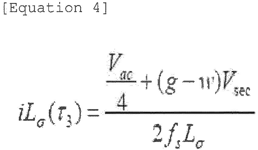
- Herein, Vac denotes an output voltage; fs denotes a switching frequency; Lτ denotes inductance; g and w denote a phase difference; and Vsec denotes an input voltage Vin. Further, I τ1_Com and I τ2_Com may denote a switch communication current at points T1 and T2 respectively.
- In order to perform zero voltage switching (ZVS), it is desired that each switching element of the full-
bridge switching part 532 and the half-bridge switching part 538 satisfies requirements of the followingEquation 5.
-
FIG. 12 is a diagram illustrating a relationship between an input voltage, an output voltage and a switching frequency. - In
FIG. 12, (a) illustrates an example where a switching frequency Fsw of the full-bridge switching part 532 and the half-bridge switching part 538 is changed in proportion to the input voltage Vin. - In this case, the
controller 550 may change the switching frequency Fsw of the full-bridge switching part 532 and the half-bridge switching part 538 in proportion to the input voltage Vin. - Then, (b) of
FIG. 12 illustrates an example where the switching frequency Fsw of the full-bridge switching part 532 and the half-bridge switching part 538 is changed in reverse proportion to the output voltage Vac. - In this case, the
controller 550 may change the switching frequency Fsw of the full-bridge switching part 532 and the half-bridge switching part 538 in reverse proportion to the output voltage Vac. - As described above with reference to
FIGS. 6 to 12 , thecontroller 550 may change the switching frequency of the full-bridge switching part 532 and the half-bridge switching part 538 in the first section Pba and Pbb, thereby enabling stable power output. - As the full-
bridge switching part 532 and the half-bridge switching part 538 are provided in theconverter 530, a turn ratio of thetransformer 536 may be reduced, and the size of thetransformer 536 may also be reduced, thereby reducing the size of thejunction box 200 including theconverter 530 and the like. - Further, as the level of the first DC power Vin, input from the
solar cell module 100, decreases, thecontroller 550 lowers the second switching frequency fb, such that even when DC power input from thesolar cell module 100 is low, stable power output may be provided without limiting the range of output power. - In addition, as the peak level of the output voltage Vac of the
inverter 540 decreases, thecontroller 550 controls the third section Pc to be increased to perform power conversion, thereby enabling stable output of AC power. - Moreover, according to the waveform of the output voltage Vac of the
inverter 540, thecontroller 550 may change the switching frequency of the full-bridge switching part 532 and the half-bridge switching part 538, thereby enabling stable output of AC power. - Further, the
controller 550 may perform two-stage power conversion by using theconverter 530 and theinverter 540, thereby improving power factor. - In addition, in another embodiment, when changing the switching frequency of the full-
bridge switching part 532 and the half-bridge switching part 538, thecontroller 550 may change the first phase difference between the full-bridge switching part 532 and the half-bridge switching part 538, thereby providing stable power output. - Moreover, in yet another embodiment, the
controller 550 may control driving of the full-bridge switching part 532 and the half-bridge switching part 538 by separating a section where the switching frequency of the full-bridge switching part 532 and the half-bridge switching part 538 is changed from a section where the switching frequency of the full-bridge switching part 532 and the half-bridge switching part 538 is constant, according to a waveform of the output voltage Vac of theinverter 540, thereby providing stable power output. -
FIG. 13 is an exploded perspective view of a solar cell module ofFIG. 3 . - Referring to
FIG. 13 , thesolar cell module 100 includes a plurality ofsolar cells 130. In addition, thesolar cell module 100 may further include afirst sealing material 120 and asecond sealing material 150 which are disposed at a lower surface and an upper surface of each of thesolar cells 130; arear substrate 110 disposed at a lower surface of thefirst sealing material 120; and afront substrate 160 disposed at an upper surface of thesecond sealing material 150. - Each of the
solar cells 130 is a semiconductor device to convert solar energy into electrical energy, and examples thereof include a silicon solar cell, a compound semiconductor solar cell, a tandem solar cell, a dye-sensitized solar cell, a CdTe solar cell, a CIGS solar cell, a thin-film solar cell, and the like. - Each of the
solar cells 130 has a light receiving surface, on which sunlight is incident, and a back surface which is opposite the light receiving surface. For example, thesolar cell 130 includes: a first conductive type silicon substrate; a second conductive type semiconductor layer formed on the silicon substrate, the second conductive type being opposite to the first conductive type; at least one or more openings through which a portion of the second conductive type semiconductor layer is exposed; an anti-reflection film formed on the second conductive type semiconductor layer; a front electrode which contacts the portion of the second conductive type semiconductor layer exposed through the at least one or more openings; and a rear electrode formed at the rear surface of the silicon substrate. - Each of the
solar cells 130 may be electrically connected in series or in parallel, or may be connected in a serial-parallel manner. Specifically, the plurality ofsolar cells 130 may be electrically connected to each other viaribbons 133. Each of theribbons 133 may be bonded to the front electrode formed on the light receiving surface of one of thesolar cells 130 and the rear electrode formed on the back surface of another adjacent one of the solar cells. - In
FIG. 13 , theribbons 133 are arranged in two rows and the plurality ofsolar cells 130 are connected in series by theribbons 133 to form onesolar cell string 140. - In this manner, as illustrated in
FIG. 3 , sixsolar cell strings - The
rear substrate 110 is a back sheet having waterproof, insulation, and ultraviolet protection functions, and may be a Tedlar/PET/Tedlar (TPT) type substrate, but is not limited thereto. Further,FIG. 4 illustrates an example where therear substrate 110 is formed in a rectangular shape, but therear substrate 110 is not limited thereto, and may be formed in various shapes, such as a circular shape and a semi-circular shape, depending on the environment where thesolar cell module 100 is installed. - The
first sealing material 120 may be attached to therear substrate 110, with the size of thefirst sealing material 120 being the same as the size of therear substrate 110, and the plurality ofsolar cells 130 may be arranged on thefirst sealing material 120, with thesolar cells 130 being adjacent to each other to form several strings. - The
second sealing material 150, which is disposed on thesolar cell 130, may be bonded to thefirst sealing material 120 by lamination - Here, the
first sealing material 120 and thesecond sealing material 150 enable elements of the solar cell to be chemically combined, and examples thereof include Ethylene Vinyl Acetate (EVA) film, and the like. - The
front substrate 160 may be disposed on thesecond sealing material 150 for sunlight transmission, and it is desired that thefront substrate 160 is made of reinforced glass to protect thesolar cells 130 from external impact and the like. Further, it is further desired that thefront substrate 160 is made of low-iron reinforced glass to prevent reflection of sunlight and to increase transmittance of sunlight. - As is apparent from the above description, according to an embodiment of the present invention, there is provided a photovoltaic module including: a solar cell module including a plurality of solar cells; a converter to convert a level of first direct current (DC) power input from the solar cell module, and to output second DC power; an inverter to convert the DC power supplied from the converter into alternating current (AC) power; and a controller to control the converter and the inverter, wherein the converter includes: a full-bridge switching part to switch the first DC power; a transformer having an input side connected to an output terminal of the full-bridge switching part; and a half-bridge switching part connected to an output side of the transformer, wherein the controller changes a switching frequency of the full-bridge switching part and the half-bridge switching part in a first section, thereby enabling stable power output.
- As the full-bridge switching part and the half-bridge switching part are provided in the converter, a turn ratio of the transformer may be reduced, and the size of the transformer may also be reduced, thereby reducing the size of the junction box including the converter and the like.
- Further, as the level of the first DC power, input from the solar cell module, decreases, the controller may lower the second switching frequency, such that even when DC power input from the solar cell module is low, stable power output may be provided without limiting the range of output power.
- In addition, as a peak level of the output voltage of the inverter decreases, the controller may control a third section to be increased to perform power conversion, thereby enabling stable output of AC power.
- Moreover, the controller may change the switching frequency of the full-bridge switching part and the half-bridge switching part according to a waveform of an output voltage of the inverter, thereby enabling stable output of AC power.
- Further, the controller may perform two-stage power conversion by using the converter and the inverter, thereby improving power factor.
- In accordance with another embodiment of the present invention, there is provided a photovoltaic module including: a solar cell module including a plurality of solar cells; a converter to convert a level of first direct current (DC) power input from the solar cell module, and to output second DC power; an inverter to convert the DC power supplied from the converter into alternating current (AC) power; and a controller to control the converter and the inverter, wherein the converter includes: a full-bridge switching part to switch the first DC power; a transformer having an input side connected to an output terminal of the full-bridge switching part; and a half-bridge switching part connected to an output side of the transformer, wherein when changing a switching frequency of the full-bridge switching part and the half-bridge switching part, the controller changes a first phase difference between the full-bridge switching part and the half-bridge switching part, thereby enabling stable power output.
- In accordance with yet another embodiment of the present invention, there is provided a photovoltaic module including: a solar cell module including a plurality of solar cells; a converter to convert a level of first direct current (DC) power input from the solar cell module, and to output second DC power; an inverter to convert the DC power supplied from the converter into alternating current (AC) power; and a controller to control the converter and the inverter, wherein the converter includes: a full-bridge switching part to switch the first DC power; a transformer having an input side connected to an output terminal of the full-bridge switching part; and a half-bridge switching part connected to an output side of the transformer, wherein the controller controls driving of the full-bridge switching part and the half-bridge switching part by separating a section where a switching frequency of the full-bridge switching part and the half-bridge switching part is changed from a section where the switching frequency of the full-bridge switching part and the half-bridge switching part is constant, according to a waveform of an output voltage of the inverter, thereby enabling stable power output.
- As described, the photovoltaic module is not limited to the configuration and method of the above-described embodiments, and all or some of the above embodiments may be selectively combined with each other to enable various modifications thereof.
- While the present disclosure has been shown and described with reference to the exemplary embodiments thereof, it should be understood that the present disclosure is not limited to the specific embodiments, and various modifications and variations may be made by those skilled in the art without departing from the scope and spirit of the invention as defined by the appended claims, and the modified implementations should not be construed independently of the technical idea or prospect of the present disclosure.
Claims (15)
- A photovoltaic module (50)comprising:a solar cell module (100) including a plurality of solar cells;a converter (530) to convert a level of first direct current (DC) power input from the solar cell module (100), and to output second DC power;an inverter (540) to convert the DC power supplied from the converter into alternating current (AC) power; anda controller (550) to control the converter (530) and the inverter (540),wherein the converter (530) comprises:a full-bridge switching part (532) to switch the first DC power;a transformer (536) having an input side connected to an output terminal of the full-bridge switching part; anda half-bridge switching part (538) connected to an output side of the transformer,wherein the controller (550) changes a switching frequency of the full-bridge switching part (532) and the half-bridge switching part (538) in a first section.
- The photovoltaic module of claim 1, wherein when changing the switching frequency of the full-bridge switching part (532) and the half-bridge switching part (538) in the first section, the controller (550) changes a first phase difference between the full-bridge switching part (532) and the half-bridge switching part (538).
- The photovoltaic module of claim 1 or 2, wherein when changing the switching frequency of the full-bridge switching part (532) and the half-bridge switching part (538) in the first section, the controller (550) changes a second phase difference between the full-bridge switching part (532) and the inverter (540).
- The photovoltaic module of any one preceding claim, wherein the full-bridge switching part (532) comprises:a first switching element (Q1) and a second switching element (Q2) which are connected in parallel with each other; anda third switching element (Q3) and a fourth switching element (Q4) which are connected in series with the first switching element (Q1) and the second switching element (Q2), respectively,wherein the input side of the transformer (536) is connected between a first node, which is between the first switching element and the second switching element, and a second node which is between the third switching element and the fourth switching element.
- The photovoltaic module of any one preceding claim, wherein the converter further comprises an inductor (Lr) connected between the transformer (536) and the half-bridge switching part (538).
- The photovoltaic module of any one preceding claim, wherein the half-bridge switching part (538) comprises:a fifth switching element (Q5) and a sixth switching element (Q6) which are connected in series; anda first capacitor (C1) and a second capacitor (C2) which are connected in series,wherein the output side of the transformer (536) is connected between a third node, which is between the fifth switching element and the sixth switching element, and a fourth node which is between the first capacitor and the second capacitor.
- The photovoltaic module of any one preceding claim, wherein the controller (550) controls a switching frequency of the inverter to be constant in the first section.
- The photovoltaic module of claim 7, wherein the switching frequency of the full-bridge switching part (532) and the half-bridge switching part (538) is greater than the switching frequency of the inverter in the first section.
- The photovoltaic module of any one preceding claim, wherein the controller (550) controls the full-bridge switching part (532) and the half-bridge switching part (538) to be driven with a first switching frequency in a second section, and controls the full-bridge switching part and the half-bridge switching part to be driven with a second switching frequency, which is lower than the first switching frequency, in a third section,
wherein the first section is disposed between the second section and the third section. - The photovoltaic module of claim 9, wherein:at a transition from the second section to the third section, the controller (550) controls the switching frequency of the full-bridge switching part (532) and the half-bridge switching part (538) to be decreased; andat a transition from the third section to the second section, the controller (550) controls the switching frequency of the full-bridge switching part (532) and the half-bridge switching part (538) to be increased.
- The photovoltaic module of claim 9 or 10, wherein as the level of the first direct current (DC) power supplied from the solar cell module decreases, the controller (550) controls the second switching frequency to be decreased.
- The photovoltaic module of any one of claims 9 to 11, wherein as a peak level of an output voltage of the inverter decreases, the controller (550) controls the third section to be increased.
- The photovoltaic module of any one preceding claim, wherein the controller (550) changes the switching frequency of the full-bridge switching part (532) and the half-bridge switching part (538) according to a waveform of an output voltage of the inverter.
- The photovoltaic module of any one of claims 5 to 13, wherein the controller (550) changes the switching frequency of the full-bridge switching part (532) and the half-bridge switching part (538) in the first section, and when changing the switching frequency, the controller controls a shape of a waveform of a current flowing through the inductor to be constant.
- The photovoltaic module of any one preceding claim, wherein the controller (550) controls driving of the full-bridge switching part (532) and the half-bridge switching part (538) by separating a section where the switching frequency of the full-bridge switching part (532) and the half-bridge switching part (538) is changed from a section where the switching frequency of the full-bridge switching part (532) and the half-bridge switching part (538) is constant, according to the waveform of the output voltage of the inverter.
Applications Claiming Priority (1)
| Application Number | Priority Date | Filing Date | Title |
|---|---|---|---|
| KR1020170122785A KR102426371B1 (en) | 2017-09-22 | 2017-09-22 | Photovoltaic module |
Publications (1)
| Publication Number | Publication Date |
|---|---|
| EP3460980A1 true EP3460980A1 (en) | 2019-03-27 |
Family
ID=63667752
Family Applications (1)
| Application Number | Title | Priority Date | Filing Date |
|---|---|---|---|
| EP18195659.0A Ceased EP3460980A1 (en) | 2017-09-22 | 2018-09-20 | Cascaded pv inverter with isolated hf stage, polarity swapping stage and output-voltage dependent switching frequency |
Country Status (4)
| Country | Link |
|---|---|
| US (1) | US11133776B2 (en) |
| EP (1) | EP3460980A1 (en) |
| JP (1) | JP7193283B2 (en) |
| KR (1) | KR102426371B1 (en) |
Cited By (1)
| Publication number | Priority date | Publication date | Assignee | Title |
|---|---|---|---|---|
| CN114257113A (en) * | 2021-11-15 | 2022-03-29 | 湖南大学 | An Active Clamped High Frequency Chain Inverter |
Families Citing this family (7)
| Publication number | Priority date | Publication date | Assignee | Title |
|---|---|---|---|---|
| CN106849167B (en) * | 2017-03-06 | 2020-03-20 | 华为技术有限公司 | Power supply system and power supply method |
| KR102577911B1 (en) * | 2018-11-16 | 2023-09-14 | 상라오 징코 솔라 테크놀러지 디벨롭먼트 컴퍼니, 리미티드 | Power converting apparatus, photovoltaic module, and photovoltaic system including the same |
| CN110190146A (en) * | 2019-07-05 | 2019-08-30 | 上海晶澳太阳能科技有限公司 | Solar cell strings and solar cell modules |
| KR20210006631A (en) | 2019-07-09 | 2021-01-19 | 엘지전자 주식회사 | Power converting apparatus and photovoltaic module including the same |
| EP3846337B1 (en) * | 2019-12-30 | 2025-09-10 | Solaredge Technologies Ltd. | Energy harvesting and electrical power generation |
| KR102390466B1 (en) * | 2020-11-30 | 2022-04-22 | ㈜한국그리드포밍 | Control method of output frequency of grid forming converter and control appratus of grid forming converter |
| CN115603347A (en) * | 2022-11-04 | 2023-01-13 | 西安飞同电器有限公司(Cn) | Wind-solar energy storage converter and control method thereof |
Citations (5)
| Publication number | Priority date | Publication date | Assignee | Title |
|---|---|---|---|---|
| WO2011102910A1 (en) * | 2010-02-22 | 2011-08-25 | Petra Solar Inc. | Method and system for controlling resonant converters used in solar inverters |
| EP2365599A1 (en) * | 2010-03-08 | 2011-09-14 | SMA Solar Technology AG | Device for converting electrical energy and method for operating such a device |
| KR20150094130A (en) * | 2014-02-10 | 2015-08-19 | 엘지전자 주식회사 | Communication device and photovoltaic system |
| US20160268890A1 (en) * | 2014-01-10 | 2016-09-15 | Sumitomo Electric Industries, Ltd. | Conversion device |
| US20170117746A1 (en) * | 2015-10-22 | 2017-04-27 | Lg Electronics Inc. | Power supply device and power supply system including the same |
Family Cites Families (7)
| Publication number | Priority date | Publication date | Assignee | Title |
|---|---|---|---|---|
| US7372709B2 (en) * | 2003-09-11 | 2008-05-13 | The Board Of Trustees Of The University Of Illinois | Power conditioning system for energy sources |
| DE102010060957A1 (en) | 2010-12-02 | 2012-06-06 | Sma Solar Technology Ag | Method for operating a DC-DC converter |
| US9948204B2 (en) * | 2011-05-19 | 2018-04-17 | Enphase Energy, Inc. | Method and apparatus for controlling resonant converter output power |
| US8699237B2 (en) * | 2012-05-30 | 2014-04-15 | National Tsing Hua University | Soft-switching inverter utilizing high step up ratio circuit with active clamping |
| US9584047B2 (en) * | 2013-03-14 | 2017-02-28 | Hdt Expeditionary Systems, Inc. | Bidirectional power converter having a charger and export modes of operation |
| US9716466B2 (en) | 2014-01-23 | 2017-07-25 | Lg Electronics Inc. | Power conversion apparatus, photovoltaic module and communication device and photovoltaic system including the same |
| US20180191165A1 (en) * | 2016-12-31 | 2018-07-05 | Sunpower Corporation | Multipolar photovolatic panel |
-
2017
- 2017-09-22 KR KR1020170122785A patent/KR102426371B1/en active Active
-
2018
- 2018-09-20 EP EP18195659.0A patent/EP3460980A1/en not_active Ceased
- 2018-09-21 JP JP2018176690A patent/JP7193283B2/en active Active
- 2018-09-21 US US16/138,429 patent/US11133776B2/en active Active
Patent Citations (5)
| Publication number | Priority date | Publication date | Assignee | Title |
|---|---|---|---|---|
| WO2011102910A1 (en) * | 2010-02-22 | 2011-08-25 | Petra Solar Inc. | Method and system for controlling resonant converters used in solar inverters |
| EP2365599A1 (en) * | 2010-03-08 | 2011-09-14 | SMA Solar Technology AG | Device for converting electrical energy and method for operating such a device |
| US20160268890A1 (en) * | 2014-01-10 | 2016-09-15 | Sumitomo Electric Industries, Ltd. | Conversion device |
| KR20150094130A (en) * | 2014-02-10 | 2015-08-19 | 엘지전자 주식회사 | Communication device and photovoltaic system |
| US20170117746A1 (en) * | 2015-10-22 | 2017-04-27 | Lg Electronics Inc. | Power supply device and power supply system including the same |
Non-Patent Citations (1)
| Title |
|---|
| HAAN DE S W H ET AL: "TEST RESULTS OF A 130 AC MODULE; A MODULAR SOLAR AC POWER STATION", WORLD CONFERENCE ON PHOTOVOLTAIC ENERGY. WAIKOLOA, DEC. 5 - 9, 1994; [WORLD CONFERENCE ON PHOTOVOLTAIC ENERGY], NEW YORK, IEEE, US, vol. CONF. 1, 5 December 1994 (1994-12-05), pages 925 - 928, XP000681354 * |
Cited By (1)
| Publication number | Priority date | Publication date | Assignee | Title |
|---|---|---|---|---|
| CN114257113A (en) * | 2021-11-15 | 2022-03-29 | 湖南大学 | An Active Clamped High Frequency Chain Inverter |
Also Published As
| Publication number | Publication date |
|---|---|
| US11133776B2 (en) | 2021-09-28 |
| KR102426371B1 (en) | 2022-07-27 |
| US20190097576A1 (en) | 2019-03-28 |
| JP7193283B2 (en) | 2022-12-20 |
| JP2019062733A (en) | 2019-04-18 |
| KR20190033976A (en) | 2019-04-01 |
Similar Documents
| Publication | Publication Date | Title |
|---|---|---|
| EP3460980A1 (en) | Cascaded pv inverter with isolated hf stage, polarity swapping stage and output-voltage dependent switching frequency | |
| EP2899867B1 (en) | Power conversion apparatus, photovoltaic module, and photovoltaic system including the same | |
| EP2621075B1 (en) | Power converting apparatus and photovoltaic module | |
| EP2897287B1 (en) | Photovoltaic module | |
| KR102631696B1 (en) | Photovoltaic module, and photovoltaic system including the same | |
| EP2911261B1 (en) | Power conversion apparatus and photovoltaic module | |
| US10715054B2 (en) | Power conversion device and photovoltaic module including the same | |
| KR102156061B1 (en) | Power converting apparatus, and photovoltaic module | |
| KR101954194B1 (en) | Power converting apparatus, and photovoltaic module | |
| KR20150094130A (en) | Communication device and photovoltaic system | |
| EP2897267B1 (en) | Power conversion apparatus and photovoltaic module including the same | |
| KR102614497B1 (en) | Power converting device and and photovoltaic module including the same | |
| KR20150085413A (en) | Photovoltaic module | |
| KR101843776B1 (en) | Photovoltaic module and photovoltaic system including the same | |
| KR20150118477A (en) | Photovoltaic module | |
| KR20150086765A (en) | Power converting apparatus, and photovoltaic module | |
| KR20160025933A (en) | Transformer and power converting apparatus icnluing the same | |
| KR20190051333A (en) | Photovoltaic module |
Legal Events
| Date | Code | Title | Description |
|---|---|---|---|
| PUAI | Public reference made under article 153(3) epc to a published international application that has entered the european phase |
Free format text: ORIGINAL CODE: 0009012 |
|
| STAA | Information on the status of an ep patent application or granted ep patent |
Free format text: STATUS: THE APPLICATION HAS BEEN PUBLISHED |
|
| AK | Designated contracting states |
Kind code of ref document: A1 Designated state(s): AL AT BE BG CH CY CZ DE DK EE ES FI FR GB GR HR HU IE IS IT LI LT LU LV MC MK MT NL NO PL PT RO RS SE SI SK SM TR |
|
| AX | Request for extension of the european patent |
Extension state: BA ME |
|
| STAA | Information on the status of an ep patent application or granted ep patent |
Free format text: STATUS: REQUEST FOR EXAMINATION WAS MADE |
|
| 17P | Request for examination filed |
Effective date: 20190913 |
|
| RBV | Designated contracting states (corrected) |
Designated state(s): AL AT BE BG CH CY CZ DE DK EE ES FI FR GB GR HR HU IE IS IT LI LT LU LV MC MK MT NL NO PL PT RO RS SE SI SK SM TR |
|
| STAA | Information on the status of an ep patent application or granted ep patent |
Free format text: STATUS: EXAMINATION IS IN PROGRESS |
|
| 17Q | First examination report despatched |
Effective date: 20200507 |
|
| RAP1 | Party data changed (applicant data changed or rights of an application transferred) |
Owner name: SHANGRAO JINKO SOLAR TECHNOLOGY DEVELOPMENT CO., LTD |
|
| RAP1 | Party data changed (applicant data changed or rights of an application transferred) |
Owner name: SHANGRAO JINKO SOLAR TECHNOLOGY DEVELOPMENT CO., LTD |
|
| RAP3 | Party data changed (applicant data changed or rights of an application transferred) |
Owner name: SHANGRAO XINYUAN YUEDONG TECHNOLOGY DEVELOPMENT CO. LTD |
|
| STAA | Information on the status of an ep patent application or granted ep patent |
Free format text: STATUS: THE APPLICATION HAS BEEN REFUSED |
|
| 18R | Application refused |
Effective date: 20231117 |