EP3460924A1 - Electrical connector equipped with signal terminals and ground terminal and electrical connector device using same electrical connector - Google Patents
Electrical connector equipped with signal terminals and ground terminal and electrical connector device using same electrical connector Download PDFInfo
- Publication number
- EP3460924A1 EP3460924A1 EP17799186.6A EP17799186A EP3460924A1 EP 3460924 A1 EP3460924 A1 EP 3460924A1 EP 17799186 A EP17799186 A EP 17799186A EP 3460924 A1 EP3460924 A1 EP 3460924A1
- Authority
- EP
- European Patent Office
- Prior art keywords
- ground terminal
- electrical connector
- signal terminals
- shell
- conductive shell
- Prior art date
- Legal status (The legal status is an assumption and is not a legal conclusion. Google has not performed a legal analysis and makes no representation as to the accuracy of the status listed.)
- Granted
Links
Images




Classifications
-
- H—ELECTRICITY
- H01—ELECTRIC ELEMENTS
- H01R—ELECTRICALLY-CONDUCTIVE CONNECTIONS; STRUCTURAL ASSOCIATIONS OF A PLURALITY OF MUTUALLY-INSULATED ELECTRICAL CONNECTING ELEMENTS; COUPLING DEVICES; CURRENT COLLECTORS
- H01R13/00—Details of coupling devices of the kinds covered by groups H01R12/70 or H01R24/00 - H01R33/00
- H01R13/648—Protective earth or shield arrangements on coupling devices, e.g. anti-static shielding
- H01R13/658—High frequency shielding arrangements, e.g. against EMI [Electro-Magnetic Interference] or EMP [Electro-Magnetic Pulse]
- H01R13/6591—Specific features or arrangements of connection of shield to conductive members
- H01R13/6597—Specific features or arrangements of connection of shield to conductive members the conductive member being a contact of the connector
-
- H—ELECTRICITY
- H01—ELECTRIC ELEMENTS
- H01R—ELECTRICALLY-CONDUCTIVE CONNECTIONS; STRUCTURAL ASSOCIATIONS OF A PLURALITY OF MUTUALLY-INSULATED ELECTRICAL CONNECTING ELEMENTS; COUPLING DEVICES; CURRENT COLLECTORS
- H01R12/00—Structural associations of a plurality of mutually-insulated electrical connecting elements, specially adapted for printed circuits, e.g. printed circuit boards [PCB], flat or ribbon cables, or like generally planar structures, e.g. terminal strips, terminal blocks; Coupling devices specially adapted for printed circuits, flat or ribbon cables, or like generally planar structures; Terminals specially adapted for contact with, or insertion into, printed circuits, flat or ribbon cables, or like generally planar structures
- H01R12/70—Coupling devices
- H01R12/71—Coupling devices for rigid printing circuits or like structures
- H01R12/72—Coupling devices for rigid printing circuits or like structures coupling with the edge of the rigid printed circuits or like structures
- H01R12/722—Coupling devices for rigid printing circuits or like structures coupling with the edge of the rigid printed circuits or like structures coupling devices mounted on the edge of the printed circuits
- H01R12/725—Coupling devices for rigid printing circuits or like structures coupling with the edge of the rigid printed circuits or like structures coupling devices mounted on the edge of the printed circuits containing contact members presenting a contact carrying strip, e.g. edge-like strip
-
- H—ELECTRICITY
- H01—ELECTRIC ELEMENTS
- H01R—ELECTRICALLY-CONDUCTIVE CONNECTIONS; STRUCTURAL ASSOCIATIONS OF A PLURALITY OF MUTUALLY-INSULATED ELECTRICAL CONNECTING ELEMENTS; COUPLING DEVICES; CURRENT COLLECTORS
- H01R13/00—Details of coupling devices of the kinds covered by groups H01R12/70 or H01R24/00 - H01R33/00
- H01R13/646—Details of coupling devices of the kinds covered by groups H01R12/70 or H01R24/00 - H01R33/00 specially adapted for high-frequency, e.g. structures providing an impedance match or phase match
- H01R13/6461—Means for preventing cross-talk
- H01R13/6463—Means for preventing cross-talk using twisted pairs of wires
-
- H—ELECTRICITY
- H01—ELECTRIC ELEMENTS
- H01R—ELECTRICALLY-CONDUCTIVE CONNECTIONS; STRUCTURAL ASSOCIATIONS OF A PLURALITY OF MUTUALLY-INSULATED ELECTRICAL CONNECTING ELEMENTS; COUPLING DEVICES; CURRENT COLLECTORS
- H01R13/00—Details of coupling devices of the kinds covered by groups H01R12/70 or H01R24/00 - H01R33/00
- H01R13/646—Details of coupling devices of the kinds covered by groups H01R12/70 or H01R24/00 - H01R33/00 specially adapted for high-frequency, e.g. structures providing an impedance match or phase match
- H01R13/6461—Means for preventing cross-talk
- H01R13/6471—Means for preventing cross-talk by special arrangement of ground and signal conductors, e.g. GSGS [Ground-Signal-Ground-Signal]
-
- H—ELECTRICITY
- H01—ELECTRIC ELEMENTS
- H01R—ELECTRICALLY-CONDUCTIVE CONNECTIONS; STRUCTURAL ASSOCIATIONS OF A PLURALITY OF MUTUALLY-INSULATED ELECTRICAL CONNECTING ELEMENTS; COUPLING DEVICES; CURRENT COLLECTORS
- H01R24/00—Two-part coupling devices, or either of their cooperating parts, characterised by their overall structure
- H01R24/60—Contacts spaced along planar side wall transverse to longitudinal axis of engagement
- H01R24/62—Sliding engagements with one side only, e.g. modular jack coupling devices
Definitions
- the present invention relates to an electrical connector equipped with signal terminals and a ground terminal, and an electrical connector device using the same.
- Patent Literature 1 An example of such an electrical connector is shown in Patent Literature 1.
- this type of electrical connector it is attempted to reduce crosstalk generated between a pair of signal terminals by arranging a ground terminal between the pair of signal terminals, which are respectively connected to a twisted pair cable and used for transmission of a differential signal.
- the ground terminal is generally connected to a drain wire housed in the pair cable or is arranged without being connected to any portion when the drain wire is not used.
- Patent Literature 1 JP-A-2010-287560
- the present invention has been made in order to solve such problems in the related art, and an object of the present invention is to provide an electrical connector capable of connecting a ground terminal to a ground with a simple structure without connection to a drain wire, and to provide an electrical connector device using the same.
- an electrical connector includes signal terminals and a ground terminal, an insulating housing for holding the signal terminals and the ground terminal, and a conductive shell covering at least a part of side outer peripheries of the signal terminals and the ground terminal, wherein the signal terminals form pairs, the ground terminal is disposed between the pairs of signal terminals, and a part of the ground terminal is in direct contact with an inner wall of the conductive shell.
- the electrical connector of this aspect by bringing the ground terminal into direct contact with the conductive shell, it is possible to connect the ground terminal to the ground with the simple structure without connection to the drain wire, and thus it is possible to simplify the structure of the device and to reduce cost of producing the device. Further, by arranging the ground terminal between the pairs of signal terminals, it is possible to suppress crosstalk occurring between the pairs of signal terminals
- the signal terminals or the ground terminal have the same size and shape in a portion located on an insertion-removal side of a mating connector with respect to a portion fixed by the insulating housing.
- the electrical connector of this aspect by making parts of the signal terminals and a part of the ground terminal have the same size and shape, it is possible to obtain effects such as easy production of the electrical connector.
- parts of the signal terminals and a part of the ground terminal are arranged in a line in a pitch direction of the signal terminals and the ground terminal in the portion located on the insertion-removal side of the mating connector with respect to the portion fixed by the insulating housing.
- the electrical connector of this aspect by arranging the parts of the signal terminals and the part of the ground terminal in a line, it is possible to obtain effects such as easy production of the electrical connector.
- a load is applied to a part of the ground terminal in direct contact with the inner wall of the conductive shell toward a side in contact with the inner wall of the conductive shell.
- the electrical connector of this aspect by applying the load in advance, it is possible to bring a part of the ground terminal into direct contact with the conductive shell by merely holding the ground terminal in the insulating housing.
- a part of the ground terminal in direct contact with the inner wall of the conductive shell is located on a side opposite to an insertion-removal side of the mating connector with respect to the portion fixed by the insulating housing.
- the electrical connector of this aspect it is possible to bring the ground terminal into contact with the conductive shell without suppressing fitting of a cable connector 10 and a board connector 70.
- a part of the ground terminal in direct contact with the inner wall of the conductive shell is located on an insertion-removal side of the mating connector with respect to the portion fixed by the insulating housing.
- the electrical connector of this aspect it is possible to bring the ground terminal into direct contact with the conductive shell without increasing the size of the electrical connector.
- a part of the ground terminal in direct contact with the inner wall of the conductive shell is provided to be slidable with respect to the inner wall of the conductive shell.
- the electrical connector of the above aspect may be paired with the mating connector to form an electrical connector device.
- an electrical connector capable of connecting a ground terminal to a ground with a simple structure without connection to a drain wire, and an electrical connector device using the same.
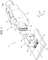
- Fig. 1 is a perspective view showing an example of a use state of an electrical connector device 1 according to a first embodiment of the present invention.
- the electrical connector device 1 includes a set of an electrical connector 10 and a mating connector 70 which can be attached to and detached from each other through insertion-removal, for example, fitting and removal work.
- the electrical connector 10 may be, for example, a cable connector connected to an electrical cable 4, and the mating connector 70 may be, for example, a board connector connected to a board 3.
- the cable connector 10 and the board connector 70 may be considered to have substantially symmetrical shapes.
- the board connector 70 mainly includes an insulating housing 72, a terminal 71 held by the insulating housing 72 with a part thereof exposed from the insulating housing 72, and, further, a conductive shell 80 substantially covering an outer periphery other than a front side and a bottom side of the insulating housing 72.
- a fitting hole 77 is provided on a front surface of the insulating housing 72, and further a fitting convex portion (not shown) matching a fitting concave portion 28 provided in an insulating housing 20 of the electrical connector 10 is provided in the fitting hole 77.
- One end side of the terminal 71 is arranged exposed in the fitting convex portion while the other end side 71A of the terminal 71 is soldered to the board 3.
- the cable connector 10 and the board connector 70 can be engaged with each other or can be disengaged by moving in an arrow " ⁇ " direction in the drawing.
- arrows " ⁇ ", “ ⁇ ", “ ⁇ ” shown in the drawing are substantially perpendicular to each other.
- a conductive shell 30 of the cable connector 10 exposed from a hood 12 and a tip end portion of the insulating housing 20 are inserted into the substantially rectangular fitting hole 77 provided on a front surface of the board connector 70, and locking portions elastically protruding from upper and lower portions of the conductive shell 30 of the cable connector 10, for example, locking projections 55 displaceable in an arrow " ⁇ " direction shown in the drawing are fitted into locked portions, for example, through-holes 85 provided on a ceiling portion and a bottom plate portion of the conductive shell 80 of the board connector 70.
- a locked state can be released by moving the locking projections 55 due to an operation of a
- Fig. 2 is a center line cross-sectional view of the cable connector 10 shown in Fig. 1
- Fig. 3 is a perspective view of Fig. 2
- Fig. 2 shows, by two-dot chain lines, the terminal 71 on the board connector 70 side and a part of the shell 80 shown in Fig. 1 , and in Figs. 2 and 3 , the hood 12 of the cable connector 10 and an outer coating portion 4a, shown in Fig. 1 , provided on the electrical cable 4 are omitted.
- one electrical cable 4 shown in Fig. 1 includes a total of four twisted pair cables 5 (only two twisted pair cables 5 are shown in Figs. 2 and 3 ).
- Each twisted pair cable 5 includes one inner tube 5b, one inner tube 5b includes two insulating coatings 5c, and each insulating coating 5c includes one conductive wire 5d.
- the cable connector 10 mainly includes the insulating housing 20, a plurality of signal terminals 11 and a ground terminal 14 held in the insulating housing 20 with parts thereof exposed from the insulating housing 20, the conductive shell 30 covering a side outer periphery substantially in a longitudinal direction of the plurality of signal terminals 11 and the ground terminal 14, and, further, the insulating hood 12 which is omitted for convenience in Figs. 2 and 3 and covers an outer periphery of the conductive shell 30.
- the conductive shell 30 covers the entire side outer periphery of the signal terminals 11 and the ground terminal 14, it is not always necessary to cover the entire thereof, but it is sufficient if the conductive shell 30 covers at least a part thereof.
- the insulating housing 20 includes a main body housing 21 and an auxiliary housing 22 housed inside the main body housing 21.
- the main body housing 21 holds a front side of the signal terminals 11 and the ground terminal 14, that is, an insertion-removal side of the cable connector 10 and the board connector 70, while the auxiliary housing 22 holds a rear side of the signal terminals 11 and the ground terminal 14 side, that is, an opposite side to the insertion-removal side of the cable connector 10 and the board connector 70.
- the main body housing 21 is formed in a tubular shape having a substantially rectangular cross-section as a whole, and includes a large diameter main body 24 and a small diameter inserted portion 25 extending from the main body 24 to the front side (insertion-removal side).
- the conductive shell 30 includes a main body shell 31, a plate-like shell 32, and a tubular shell 33. Any of them are produced by punching and bending a single metal plate, and have some elasticity.
- the main body shell 31, the plate-like shell 32, and the tubular shell 33 are physically and electrically connected to each other, so that any of them can exert a ground function.
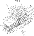
- Fig. 4 is a perspective view in which the plate-like shell 32 is removed from Fig. 3 .
- the main body shell 31 has a substantially C-shaped cross-section as a whole, and mainly covers a side outer periphery of the main body 24 of the insulating housing 20 and a part of a side outer periphery of the auxiliary housing 22.
- the main body shell 31 is provided with an elastic arm 50 connected by a support portion 44, the locking projection 55 shown in Fig. 1 is formed as a part of the elastic arm 50, and the button 13 for operating the locking projection 55 is fixed to the elastic arm 50.
- the plate-like shell 32 has a substantially U-shaped cross-section as a whole, and is mainly attached to the main body shell 31, to cover the side outer periphery of the main body 24 of the insulating housing 20 and the side outer periphery of the auxiliary housing 22, which are not covered by the main body shell 31.
- the tubular shell 33 is a tubular body having a substantially rectangular cross-section as a whole and mainly covers an outer periphery of the inserted portion 25 of the insulating housing 20.
- the tubular shell 33 has a tubular main body 60, and a standing piece 64, a stepped portion 61a, and a stepped portion 63a, which extend radially from the main body 60.
- the main body 60 is connected to a part of the shell 80 of the board connector 70 (see Fig. 2 ), and through this connection, the conductive shell 30 of the cable connector 10 and the shell 80 of the board connector 70 are electrically connected to each other.
- the tubular shell 33 is stably positioned with respect to the insulating housing 20 and the main body shell 31 by inserting the inserted portion 25 of the insulating housing 20 into the main body 60 and abutting the standing piece 64, the stepped portion 61a, and the stepped portion 63a against predetermined portions of the insulating housing 20 and the main body shell 31.
- the tubular shell 33 can be fixed to the insulating housing 20, for example, by fitting a locking protrusion 24b protruding to an outer surface of the insulating housing 20 into a locking hole 61b of an attachment piece 61 extending toward the main body shell 31 via the stepped portion 61a, and so as to sandwich an attachment piece 63 connected to the stepped portion 63a from the outside by the main body shell 31.
- the signal terminal 11 and the ground terminal 14 may be produced by punching and bending a single metal plate.
- Figs. 5 and 6 show an arrangement state of the signal terminals 11 and the ground terminal 14 in the insulating housing 20.
- Fig. 5 is a perspective view showing the arrangement state
- Fig. 6 is a front view of the arrangement state.
- the signal terminals 11 and the ground terminals 14 form two sets of terminal groups.
- Each terminal group includes four signal terminals 11 and one ground terminal 14, which are horizontally arranged at the same pitch in the " ⁇ " direction, in an order of the signal terminal 11, the signal terminal 11, the ground terminal 14, the signal terminal 11, and the signal terminal 11 in this order.
- two adjacent signal terminals 11 respectively arranged on the left and right sides with the ground terminal 14 therebetween form pairs 11A and 11B for transmitting differential signals, and two conductive wires for transmitting the differential signals included in each twisted pair cable are respectively connected to the two signal terminals 11 included in each pair.
- the one ground terminal 14 is disposed to be sandwiched from both sides between the pair 11A and the pair 11B which are the two sets of signal terminals 11 arranged in the " ⁇ " direction. In this manner, by arranging the ground terminal 14 between the pair 11A and the pair 11B of the signal terminals 11, it is possible to suppress crosstalk between the pairs.
- the two sets of terminal groups are respectively arranged at a position of sandwiching the fitting convex portion (not shown) of the board connector 70, for example, so as to face each other with the fitting concave portion 28 therebetween on an "upper side” and a “lower side” in an example of Figs. 5 and 6 .
- the upper terminal group 11', 14' and the lower terminal group 11, 14 are shifted one pitch from each other in the " ⁇ " direction.
- the terminal included in the upper terminal group is shown by adding ""' to the same reference numeral as the terminal included in the lower terminal group.
- Each signal terminal 11 includes, substantially in the longitudinal direction, a base portion 11a, a contact point 11d located on the front side with respect to the base portion 11a, a conductive wire attachment portion 11b located on the rear side (opposite side to the insertion-extraction side) with respect to a base portion 14a, and a neck portion 11c connecting the base portion 14a and the conductive wire attachment portion 11b.
- the base portion 11a is formed wide and fixed to the main body 24 (see Fig. 2 and the like) of the main body housing 21 constituting the insulating housing 20 by press fitting or the like, and the conductive wire attachment portion 11b is fixed to the auxiliary housing 22 (see Fig. 2 and the like) constituting the housing 20 by press fitting or the like. As shown in Figs.
- Fig. 7 is a schematic perspective view showing the attachment state of the signal terminal 11 and the twisted pair cable 5
- Fig. 8 is a plan view of the attachment state.
- the contact point 11d can contact the predetermined terminal 71 of the board connector 70 (like the ground terminal 14 shown in Fig. 2 ) when the cable connector 10 and the board connector 70 are fitted together.
- each ground terminal 14 includes a base portion 14a, a contact point 14d located on the front side with respect to the base portion 14a, a shell contact portion 14e located on the rear side with respect to the base portion 14a, and a neck portion 14c connecting the base portion 14a and the shell contact portion 14e.
- the base portion 14a is fixed to the main body 24 (see Fig. 2 and the like) of the main body housing 21 constituting the insulating housing 20 by press fitting or the like.
- the contact point 14d can contact the predetermined terminal 71 of the board connector 70 (see Fig. 2 ) when the cable connector 10 and the board connector 70 are fitted together.
- the shell contact portion 14e is used in a state of being always in contact with an inner wall of the conductive shell 30.
- An end portion 14h' of an upper shell contact portion 14e' is in direct contact with an inner wall 32a of the plate-like shell 32 constituting the conductive shell 30, and an end portion 14h of a lower shell contact portion 14e is in direct contact with an inner wall 31a of the main body shell 31 constituting the conductive shell 30.
- the shell contact portion 14e is located on the rear side with respect to the base portion 14a fixed to the insulating housing 20, the fitting between the cable connector 10 and the board connector 70 is not hindered.
- the term "direct contact” as used herein means that they are electrically in direct contact with each other, and accordingly includes contact via solder, conductive resin or the like.
- the neck portion 14c is bent toward the conductive shell 30.
- a load is applied to the shell contact portion 14e in advance toward a side in contact with the inner walls 31a, 32a of the conductive shell 30 by using the neck portion 14c or the like.
- front ends 11f and 14f of the signal terminal 11 and the ground terminal 14 are arranged in vertically elongated housing grooves 25a of the insulating housing 20. At this time, the front ends 11f and 14f are opposed to the conductive shell 30 via a partition wall 25c of a main body 25 of the insulating housing 20, and do not come into contact with the conductive shell 30.
- An opening 25b is provided in an upper portion of each housing groove 25a, so that vicinities of the contact points 11d and 14d of the signal terminal 11 and the ground terminal 14 are exposed to the fitting concave portion 28 of the insulating housing 20.
- the base portions 11a and 14a of the signal terminal 11 and the ground terminal 14 and portions located on the front side with respect to the base portions 11a and 14a, for example, the contact points 11d, 14d, the front ends 11f, 14f, and the like have the same size and shape. By making the same size and shape, it is possible to facilitate production of the electrical connector.
- the base portions 11a and 14a of the signal terminal 11 and the ground terminal 14 constituting each terminal group and portions located on the front side with respect to the base portions 11a and 14a, for example, the contact points 11d, 14d, the front ends 11f, 14f and the like are arranged in a line in a pitch direction " ⁇ " of the signal terminal 11 and the ground terminal 14. This can facilitate the production of the electrical connector.
- the upper and lower signal terminals 11 or the upper and lower ground terminals 14 all have the same size and shape.
- Figs. 9 to 11 show a second embodiment of the present invention. These Figs. 9 to 11 respectively correspond to Figs. 2 to 4 .
- the same members as in the first embodiment are denoted by the same reference numerals.
- the shell contact portion 14e is located on the rear side with respect to the base portion 14a fixed to the insulating housing 20, whereas in the second embodiment, the shell contact portion 15e is located on the front side with respect to the base portion 15a fixed to the insulating housing 20. According to this structure, it is possible to bring the ground terminal 14 into direct contact with the conductive shell 30 without increasing the size of the electrical connector.
- a front end 15e of a ground terminal 15 is used as a shell contact portion.
- This shell contact portion 15e is in direct contact with an inner wall 60a of the conductive shell 30 without the insulating housing 20. Since the shell contact portion 15e is provided in the vicinity of the contact point 15d with the board connector 70, when the cable connector 10 and the board connector 70 are fitted together or when the fitting is released, there is a possibility that the shell contact portion 15e moves with respect to the inner wall 60a. It is preferred that the shell contact portion 15e of the ground terminal 15 is provided to be slidable with respect to the inner wall 60a of the conductive shell 30 in order to suppress scraping or the like of the insulating housing 20 during movement of the shell contact portion 15e.
Landscapes
- Details Of Connecting Devices For Male And Female Coupling (AREA)
Abstract
Description
- The present invention relates to an electrical connector equipped with signal terminals and a ground terminal, and an electrical connector device using the same.
- An example of such an electrical connector is shown in
Patent Literature 1. In this type of electrical connector, it is attempted to reduce crosstalk generated between a pair of signal terminals by arranging a ground terminal between the pair of signal terminals, which are respectively connected to a twisted pair cable and used for transmission of a differential signal. In this case, the ground terminal is generally connected to a drain wire housed in the pair cable or is arranged without being connected to any portion when the drain wire is not used. - Patent Literature 1:
JP-A-2010-287560 - When the ground terminal is connected to the drain wire, the crosstalk can be reduced more efficiently, however, work of connecting the ground terminal to the drain wire is complicated, resulting in an increase in product cost. On the other hand, when the drain wire is not used, problem of the crosstalk naturally tends to become apparent, and particularly in recent years, as a size of the connector is reduced, a pitch between the terminals is reduced, and since high-speed transmission of high-frequency signal is desired, the problem of crosstalk becomes larger.
- The present invention has been made in order to solve such problems in the related art, and an object of the present invention is to provide an electrical connector capable of connecting a ground terminal to a ground with a simple structure without connection to a drain wire, and to provide an electrical connector device using the same.
- In order to solve the above problem, an electrical connector according to an aspect of the present invention includes signal terminals and a ground terminal, an insulating housing for holding the signal terminals and the ground terminal, and a conductive shell covering at least a part of side outer peripheries of the signal terminals and the ground terminal, wherein the signal terminals form pairs, the ground terminal is disposed between the pairs of signal terminals, and a part of the ground terminal is in direct contact with an inner wall of the conductive shell.
- According to the electrical connector of this aspect, by bringing the ground terminal into direct contact with the conductive shell, it is possible to connect the ground terminal to the ground with the simple structure without connection to the drain wire, and thus it is possible to simplify the structure of the device and to reduce cost of producing the device. Further, by arranging the ground terminal between the pairs of signal terminals, it is possible to suppress crosstalk occurring between the pairs of signal terminals
- In the electrical connector of the above aspect, it is preferred that the signal terminals or the ground terminal have the same size and shape in a portion located on an insertion-removal side of a mating connector with respect to a portion fixed by the insulating housing.
- According to the electrical connector of this aspect, by making parts of the signal terminals and a part of the ground terminal have the same size and shape, it is possible to obtain effects such as easy production of the electrical connector.
- In the electrical connector of the above aspect, it is preferred that parts of the signal terminals and a part of the ground terminal are arranged in a line in a pitch direction of the signal terminals and the ground terminal in the portion located on the insertion-removal side of the mating connector with respect to the portion fixed by the insulating housing.
- According to the electrical connector of this aspect, by arranging the parts of the signal terminals and the part of the ground terminal in a line, it is possible to obtain effects such as easy production of the electrical connector.
- In the electrical connector of the above aspect, it is preferred that a load is applied to a part of the ground terminal in direct contact with the inner wall of the conductive shell toward a side in contact with the inner wall of the conductive shell.
- According to the electrical connector of this aspect, by applying the load in advance, it is possible to bring a part of the ground terminal into direct contact with the conductive shell by merely holding the ground terminal in the insulating housing.
- In the electrical connector of the above aspect, it is preferred that a part of the ground terminal in direct contact with the inner wall of the conductive shell is located on a side opposite to an insertion-removal side of the mating connector with respect to the portion fixed by the insulating housing.
- According to the electrical connector of this aspect, it is possible to bring the ground terminal into contact with the conductive shell without suppressing fitting of a
cable connector 10 and aboard connector 70. - In the electrical connector of the above aspect, it is preferred that a part of the ground terminal in direct contact with the inner wall of the conductive shell is located on an insertion-removal side of the mating connector with respect to the portion fixed by the insulating housing.
- According to the electrical connector of this aspect, it is possible to bring the ground terminal into direct contact with the conductive shell without increasing the size of the electrical connector.
- In the electrical connector of the above aspect, it is preferred that a part of the ground terminal in direct contact with the inner wall of the conductive shell is provided to be slidable with respect to the inner wall of the conductive shell.
- According to the electrical connector of this aspect, it is possible to smoothly make contact between the ground terminal and the terminal of the mating connector.
- The electrical connector of the above aspect may be paired with the mating connector to form an electrical connector device.
- According to the present invention, it is possible to provide an electrical connector capable of connecting a ground terminal to a ground with a simple structure without connection to a drain wire, and an electrical connector device using the same.
-
-
Fig. 1 is a perspective view of an electrical connector device according to a first embodiment of the present invention. -
Fig. 2 is a center line cross-sectional view of an electrical connector according to the first embodiment of the present invention. -
Fig. 3 is a perspective view ofFig. 2 . -
Fig. 4 is a perspective view in which a plate-like shell is removed fromFig. 3 . -
Fig. 5 is a perspective view showing an arrangement state of terminals. -
Fig. 6 is a front view ofFig. 5 . -
Fig. 7 is a schematic perspective view showing an attachment state of a signal terminal and a twisted pair cable. -
Fig. 8 is a plan view ofFig. 7 . -
Fig. 9 is a center line cross-sectional view of the electrical connector according to a second embodiment of the present invention. -
Fig. 10 is a perspective view ofFig. 9 . -
Fig. 11 is a perspective view in which the plate-like shell is removed fromFig. 9 . - Hereinafter, an electrical connector according to a preferred embodiment of the present invention and an electrical connector device using the same will be described with reference to the accompanying drawings.
-
Fig. 1 is a perspective view showing an example of a use state of anelectrical connector device 1 according to a first embodiment of the present invention. Theelectrical connector device 1 includes a set of anelectrical connector 10 and amating connector 70 which can be attached to and detached from each other through insertion-removal, for example, fitting and removal work. Theelectrical connector 10 may be, for example, a cable connector connected to anelectrical cable 4, and themating connector 70 may be, for example, a board connector connected to aboard 3. Thecable connector 10 and theboard connector 70 may be considered to have substantially symmetrical shapes. - The
board connector 70 mainly includes aninsulating housing 72, aterminal 71 held by theinsulating housing 72 with a part thereof exposed from theinsulating housing 72, and, further, aconductive shell 80 substantially covering an outer periphery other than a front side and a bottom side of theinsulating housing 72. - A
fitting hole 77 is provided on a front surface of theinsulating housing 72, and further a fitting convex portion (not shown) matching a fittingconcave portion 28 provided in aninsulating housing 20 of theelectrical connector 10 is provided in thefitting hole 77. One end side of theterminal 71 is arranged exposed in the fitting convex portion while theother end side 71A of theterminal 71 is soldered to theboard 3. - The
cable connector 10 and theboard connector 70 can be engaged with each other or can be disengaged by moving in an arrow "α" direction in the drawing. Here, arrows "α", "β", "γ" shown in the drawing are substantially perpendicular to each other. When thecable connector 10 and theboard connector 70 are fitted together, aconductive shell 30 of thecable connector 10 exposed from ahood 12 and a tip end portion of theinsulating housing 20 are inserted into the substantiallyrectangular fitting hole 77 provided on a front surface of theboard connector 70, and locking portions elastically protruding from upper and lower portions of theconductive shell 30 of thecable connector 10, for example,locking projections 55 displaceable in an arrow "β" direction shown in the drawing are fitted into locked portions, for example, through-holes 85 provided on a ceiling portion and a bottom plate portion of theconductive shell 80 of theboard connector 70. As a result, fitting between thecable connector 10 and theboard connector 70 is locked. A locked state can be released by moving thelocking projections 55 due to an operation of abutton 13 provided on thecable connector 10. -
Fig. 2 is a center line cross-sectional view of thecable connector 10 shown inFig. 1 , andFig. 3 is a perspective view ofFig. 2 . For the sake of clarity,Fig. 2 shows, by two-dot chain lines, theterminal 71 on theboard connector 70 side and a part of theshell 80 shown inFig. 1 , and inFigs. 2 and3 , thehood 12 of thecable connector 10 and anouter coating portion 4a, shown inFig. 1 , provided on theelectrical cable 4 are omitted. As is apparent from the drawings, oneelectrical cable 4 shown inFig. 1 includes a total of four twisted pair cables 5 (only twotwisted pair cables 5 are shown inFigs. 2 and3 ). Eachtwisted pair cable 5 includes oneinner tube 5b, oneinner tube 5b includes twoinsulating coatings 5c, and each insulatingcoating 5c includes oneconductive wire 5d. - The
cable connector 10 mainly includes theinsulating housing 20, a plurality ofsignal terminals 11 and aground terminal 14 held in theinsulating housing 20 with parts thereof exposed from theinsulating housing 20, theconductive shell 30 covering a side outer periphery substantially in a longitudinal direction of the plurality ofsignal terminals 11 and theground terminal 14, and, further, theinsulating hood 12 which is omitted for convenience inFigs. 2 and3 and covers an outer periphery of theconductive shell 30. Although it is preferred that theconductive shell 30 covers the entire side outer periphery of thesignal terminals 11 and theground terminal 14, it is not always necessary to cover the entire thereof, but it is sufficient if theconductive shell 30 covers at least a part thereof. - The insulating
housing 20 includes amain body housing 21 and anauxiliary housing 22 housed inside themain body housing 21. Themain body housing 21 holds a front side of thesignal terminals 11 and theground terminal 14, that is, an insertion-removal side of thecable connector 10 and theboard connector 70, while theauxiliary housing 22 holds a rear side of thesignal terminals 11 and theground terminal 14 side, that is, an opposite side to the insertion-removal side of thecable connector 10 and theboard connector 70. Themain body housing 21 is formed in a tubular shape having a substantially rectangular cross-section as a whole, and includes a large diametermain body 24 and a small diameter insertedportion 25 extending from themain body 24 to the front side (insertion-removal side). - The
conductive shell 30 includes amain body shell 31, a plate-like shell 32, and atubular shell 33. Any of them are produced by punching and bending a single metal plate, and have some elasticity. Themain body shell 31, the plate-like shell 32, and thetubular shell 33 are physically and electrically connected to each other, so that any of them can exert a ground function. -
Fig. 4 is a perspective view in which the plate-like shell 32 is removed fromFig. 3 . Themain body shell 31 has a substantially C-shaped cross-section as a whole, and mainly covers a side outer periphery of themain body 24 of the insulatinghousing 20 and a part of a side outer periphery of theauxiliary housing 22. Themain body shell 31 is provided with anelastic arm 50 connected by asupport portion 44, the lockingprojection 55 shown inFig. 1 is formed as a part of theelastic arm 50, and thebutton 13 for operating the lockingprojection 55 is fixed to theelastic arm 50. - The plate-
like shell 32 has a substantially U-shaped cross-section as a whole, and is mainly attached to themain body shell 31, to cover the side outer periphery of themain body 24 of the insulatinghousing 20 and the side outer periphery of theauxiliary housing 22, which are not covered by themain body shell 31. - The
tubular shell 33 is a tubular body having a substantially rectangular cross-section as a whole and mainly covers an outer periphery of the insertedportion 25 of the insulatinghousing 20. Thetubular shell 33 has a tubularmain body 60, and a standingpiece 64, a steppedportion 61a, and a steppedportion 63a, which extend radially from themain body 60. When thecable connector 10 and theboard connector 70 are fitted together, themain body 60 is connected to a part of theshell 80 of the board connector 70 (seeFig. 2 ), and through this connection, theconductive shell 30 of thecable connector 10 and theshell 80 of theboard connector 70 are electrically connected to each other. Thetubular shell 33 is stably positioned with respect to the insulatinghousing 20 and themain body shell 31 by inserting the insertedportion 25 of the insulatinghousing 20 into themain body 60 and abutting the standingpiece 64, the steppedportion 61a, and the steppedportion 63a against predetermined portions of the insulatinghousing 20 and themain body shell 31. Thetubular shell 33 can be fixed to the insulatinghousing 20, for example, by fitting a lockingprotrusion 24b protruding to an outer surface of the insulatinghousing 20 into alocking hole 61b of anattachment piece 61 extending toward themain body shell 31 via the steppedportion 61a, and so as to sandwich anattachment piece 63 connected to the steppedportion 63a from the outside by themain body shell 31. - The
signal terminal 11 and theground terminal 14 may be produced by punching and bending a single metal plate.Figs. 5 and 6 show an arrangement state of thesignal terminals 11 and theground terminal 14 in the insulatinghousing 20.Fig. 5 is a perspective view showing the arrangement state, andFig. 6 is a front view of the arrangement state. - The
signal terminals 11 and theground terminals 14 form two sets of terminal groups. Each terminal group includes foursignal terminals 11 and oneground terminal 14, which are horizontally arranged at the same pitch in the "β" direction, in an order of thesignal terminal 11, thesignal terminal 11, theground terminal 14, thesignal terminal 11, and thesignal terminal 11 in this order. In each terminal group, twoadjacent signal terminals 11 respectively arranged on the left and right sides with theground terminal 14 therebetween form pairs 11A and 11B for transmitting differential signals, and two conductive wires for transmitting the differential signals included in each twisted pair cable are respectively connected to the twosignal terminals 11 included in each pair. The oneground terminal 14 is disposed to be sandwiched from both sides between thepair 11A and thepair 11B which are the two sets ofsignal terminals 11 arranged in the "β" direction. In this manner, by arranging theground terminal 14 between thepair 11A and thepair 11B of thesignal terminals 11, it is possible to suppress crosstalk between the pairs. - The two sets of terminal groups are respectively arranged at a position of sandwiching the fitting convex portion (not shown) of the
board connector 70, for example, so as to face each other with the fittingconcave portion 28 therebetween on an "upper side" and a "lower side" in an example ofFigs. 5 and 6 . As is well shown inFig. 6 , the upper terminal group 11', 14' and thelower terminal group - Each
signal terminal 11 includes, substantially in the longitudinal direction, abase portion 11a, acontact point 11d located on the front side with respect to thebase portion 11a, a conductivewire attachment portion 11b located on the rear side (opposite side to the insertion-extraction side) with respect to abase portion 14a, and aneck portion 11c connecting thebase portion 14a and the conductivewire attachment portion 11b. Thebase portion 11a is formed wide and fixed to the main body 24 (seeFig. 2 and the like) of themain body housing 21 constituting the insulatinghousing 20 by press fitting or the like, and the conductivewire attachment portion 11b is fixed to the auxiliary housing 22 (seeFig. 2 and the like) constituting thehousing 20 by press fitting or the like. As shown inFigs. 7 and 8 , theconductive wires 5d included in thetwisted pair cables 5 are respectively attached to theconductor attachment portions 11b fixed to theauxiliary housing 22. Here,Fig. 7 is a schematic perspective view showing the attachment state of thesignal terminal 11 and thetwisted pair cable 5, andFig. 8 is a plan view of the attachment state. Thecontact point 11d can contact thepredetermined terminal 71 of the board connector 70 (like theground terminal 14 shown inFig. 2 ) when thecable connector 10 and theboard connector 70 are fitted together. - On the other hand, each
ground terminal 14 includes abase portion 14a, acontact point 14d located on the front side with respect to thebase portion 14a, ashell contact portion 14e located on the rear side with respect to thebase portion 14a, and aneck portion 14c connecting thebase portion 14a and theshell contact portion 14e. Thebase portion 14a is fixed to the main body 24 (seeFig. 2 and the like) of themain body housing 21 constituting the insulatinghousing 20 by press fitting or the like. Thecontact point 14d can contact thepredetermined terminal 71 of the board connector 70 (seeFig. 2 ) when thecable connector 10 and theboard connector 70 are fitted together. - As shown in
Figs. 2 to 4 and the like, theshell contact portion 14e is used in a state of being always in contact with an inner wall of theconductive shell 30. Anend portion 14h' of an uppershell contact portion 14e' is in direct contact with aninner wall 32a of the plate-like shell 32 constituting theconductive shell 30, and anend portion 14h of a lowershell contact portion 14e is in direct contact with aninner wall 31a of themain body shell 31 constituting theconductive shell 30. In this way, by bringing theground terminal 14 and theconductive shell 30 into direct contact with each other, it is not necessary to connect the drain wire included in the cable connector to the ground terminal. As a result, it is possible to simplify a structure of the device, and to reduce cost of producing the device. Since theshell contact portion 14e is located on the rear side with respect to thebase portion 14a fixed to the insulatinghousing 20, the fitting between thecable connector 10 and theboard connector 70 is not hindered. Incidentally, the term "direct contact" as used herein means that they are electrically in direct contact with each other, and accordingly includes contact via solder, conductive resin or the like. - In order to bring the
shell contact portion 14e into contact with theconductive shell 30, theneck portion 14c is bent toward theconductive shell 30. Prior to fixing theground terminal 14 to the insulatinghousing 20, it is preferred that a load is applied to theshell contact portion 14e in advance toward a side in contact with theinner walls conductive shell 30 by using theneck portion 14c or the like. Thus, by merely holding the ground terminal in the insulating housing, it is possible to bring a part of the ground terminal into direct contact with the conductive shell. - As shown in
Figs. 2 to 4 and the like,front ends signal terminal 11 and theground terminal 14 are arranged in vertically elongatedhousing grooves 25a of the insulatinghousing 20. At this time, the front ends 11f and 14f are opposed to theconductive shell 30 via apartition wall 25c of amain body 25 of the insulatinghousing 20, and do not come into contact with theconductive shell 30. Anopening 25b is provided in an upper portion of eachhousing groove 25a, so that vicinities of the contact points 11d and 14d of thesignal terminal 11 and theground terminal 14 are exposed to the fittingconcave portion 28 of the insulatinghousing 20. When thecable connector 10 and theboard connector 70 are fitted together, thesignal terminal 11 and theground terminal 14 can be brought into contact with predetermined terminals 71 (seeFig. 1 ) of theboard connector 70 through theopenings 25b. - It is preferred that the
base portions signal terminal 11 and theground terminal 14 and portions located on the front side with respect to thebase portions contact points front ends - Further, it is preferred that the
base portions signal terminal 11 and theground terminal 14 constituting each terminal group and portions located on the front side with respect to thebase portions contact points front ends signal terminal 11 and theground terminal 14. This can facilitate the production of the electrical connector. - For the same reason, it is preferred that the upper and
lower signal terminals 11 or the upper andlower ground terminals 14 all have the same size and shape. -
Figs. 9 to 11 show a second embodiment of the present invention. TheseFigs. 9 to 11 respectively correspond toFigs. 2 to 4 . In the second embodiment, the same members as in the first embodiment are denoted by the same reference numerals. - In the first embodiment, the
shell contact portion 14e is located on the rear side with respect to thebase portion 14a fixed to the insulatinghousing 20, whereas in the second embodiment, theshell contact portion 15e is located on the front side with respect to thebase portion 15a fixed to the insulatinghousing 20. According to this structure, it is possible to bring theground terminal 14 into direct contact with theconductive shell 30 without increasing the size of the electrical connector. - In the second embodiment, a
front end 15e of aground terminal 15 is used as a shell contact portion. Thisshell contact portion 15e is in direct contact with aninner wall 60a of theconductive shell 30 without the insulatinghousing 20. Since theshell contact portion 15e is provided in the vicinity of thecontact point 15d with theboard connector 70, when thecable connector 10 and theboard connector 70 are fitted together or when the fitting is released, there is a possibility that theshell contact portion 15e moves with respect to theinner wall 60a. It is preferred that theshell contact portion 15e of theground terminal 15 is provided to be slidable with respect to theinner wall 60a of theconductive shell 30 in order to suppress scraping or the like of the insulatinghousing 20 during movement of theshell contact portion 15e. - It should be noted that the present invention is not limited to the above-described embodiments, and various other modifications can be made. It is therefore to be understood that the embodiments disclosed herein are merely illustrative and not restrictive and that the scope of the present invention should be defined not by the above description but by the appended claims, and includes all changes in the meanings equivalent to claims and within the scope of claims.
-
- 1:
- Electrical connector device
- 4:
- Electrical cable
- 5:
- Twisted pair cable
- 10:
- Cable connector (electrical connector)
- 11:
- Signal terminal
- 11a:
- Base portion (fixed portion)
- 11b:
- Conductive wire attachment portion
- 14:
- Ground terminal
- 14a:
- Base portion (fixed portion)
- 14e:
- Shell contact portion
- 14h:
- End portion
- 15:
- Ground terminal
- 20:
- Insulating housing
- 30:
- Conductive shell
- 70:
- Board connector (mating connector)
- 71:
- Terminal
- 72:
- Insulating housing
- 80:
- Conductive shell
Claims (8)
- An electrical connector comprising:signal terminals and a ground terminal;an insulating housing for holding the signal terminals and the ground terminal; anda conductive shell covering at least a part of side outer peripheries of the signal terminals and the ground terminal, whereinthe signal terminals form pairs, the ground terminal is disposed between the pairs of signal terminals, and a part of the ground terminal is in direct contact with an inner wall of the conductive shell.
- The electrical connector according to claim 1, wherein
the signal terminals or the ground terminal have the same size and shape in a portion located on an insertion-removal side of a mating connector with respect to a portion fixed by the insulating housing. - The electrical connector according to claim 1 or 2, wherein
parts of the signal terminals and a part of the ground terminal are arranged in a line in a pitch direction of the signal terminals and the ground terminal in a portion located on an insertion-removal side of a mating connector with respect to a portion fixed by the insulating housing. - The electrical connector according to any one of claims 1 to 3, wherein
a load is applied to a part of the ground terminal in direct contact with the inner wall of the conductive shell toward a side in contact with the inner wall of the conductive shell. - The electrical connector according to any one of claims 1 to 4, wherein
a part of the ground terminal in direct contact with the inner wall of the conductive shell is located on a side opposite to an insertion-removal side of a mating connector with respect to a portion fixed by the insulating housing. - The electrical connector according to any one of claims 1 to 4, wherein
a part of the ground terminal in direct contact with the inner wall of the conductive shell is located on an insertion-removal side of a mating connector with respect to a portion fixed by the insulating housing. - The electrical connector according to claim 6, wherein
a part of the ground terminal in direct contact with the inner wall of the conductive shell is provided to be slidable with respect to the inner wall of the conductive shell. - An electrical connector device comprising the electrical connector according to any one of claims 1 to 7 and a mating connector.
Applications Claiming Priority (2)
| Application Number | Priority Date | Filing Date | Title |
|---|---|---|---|
| JP2016097943A JP6761665B2 (en) | 2016-05-16 | 2016-05-16 | An electric connector equipped with a signal terminal and a ground terminal, and an electric connector device using the electric connector. |
| PCT/JP2017/017214 WO2017199756A1 (en) | 2016-05-16 | 2017-05-02 | Electrical connector equipped with signal terminals and ground terminal and electrical connector device using same electrical connector |
Publications (3)
| Publication Number | Publication Date |
|---|---|
| EP3460924A1 true EP3460924A1 (en) | 2019-03-27 |
| EP3460924A4 EP3460924A4 (en) | 2020-01-22 |
| EP3460924B1 EP3460924B1 (en) | 2022-11-16 |
Family
ID=60325079
Family Applications (1)
| Application Number | Title | Priority Date | Filing Date |
|---|---|---|---|
| EP17799186.6A Active EP3460924B1 (en) | 2016-05-16 | 2017-05-02 | Electrical connector equipped with signal terminals and ground terminal and electrical connector device using same electrical connector |
Country Status (5)
| Country | Link |
|---|---|
| US (1) | US10355422B2 (en) |
| EP (1) | EP3460924B1 (en) |
| JP (1) | JP6761665B2 (en) |
| CN (1) | CN209045922U (en) |
| WO (1) | WO2017199756A1 (en) |
Families Citing this family (6)
| Publication number | Priority date | Publication date | Assignee | Title |
|---|---|---|---|---|
| USD852142S1 (en) * | 2015-12-03 | 2019-06-25 | Hirose Electric Co., Ltd. | Electrical connector |
| JP7404142B2 (en) | 2020-04-17 | 2023-12-25 | 日本航空電子工業株式会社 | Connectors, harnesses and connector assemblies |
| USD1054989S1 (en) * | 2021-03-09 | 2024-12-24 | Hirose Electric Co., Ltd. | Electric connector |
| CN115347423B (en) * | 2021-05-13 | 2025-09-16 | 泰科电子(上海)有限公司 | Electric connector assembly |
| JP7563319B2 (en) * | 2021-07-16 | 2024-10-08 | 住友電装株式会社 | Connectors and Wire Harnesses |
| JP2023100475A (en) * | 2022-01-06 | 2023-07-19 | 株式会社村田製作所 | Electrical connector and electrical connector set comprising the electrical connector |
Family Cites Families (16)
| Publication number | Priority date | Publication date | Assignee | Title |
|---|---|---|---|---|
| US6447311B1 (en) * | 2001-12-28 | 2002-09-10 | Hon Hai Precision Ind, Co., Ltd. | Electrical connector with grounding means |
| US7744418B2 (en) * | 2006-07-18 | 2010-06-29 | Hon Hai Precision Ind. Co., Ltd. | Upright electrical connector |
| CN200972963Y (en) * | 2006-10-16 | 2007-11-07 | 富士康(昆山)电脑接插件有限公司 | Electric connector |
| JP4519181B2 (en) * | 2008-05-14 | 2010-08-04 | ヒロセ電機株式会社 | connector |
| CN101771225B (en) | 2009-01-07 | 2012-07-04 | 富士康(昆山)电脑接插件有限公司 | Application of electric connector |
| US8142209B2 (en) | 2009-01-07 | 2012-03-27 | Hon Hai Precision Ind. Co., Ltd. | Electrical connector with improved contacts arrangement |
| JP2010267503A (en) | 2009-05-15 | 2010-11-25 | Hosiden Corp | Connector |
| JP2013229154A (en) * | 2012-04-25 | 2013-11-07 | Hirose Electric Co Ltd | Power supply electrode connection member |
| US9356404B2 (en) * | 2013-09-25 | 2016-05-31 | Hon Hai Precision Industry Co., Ltd. | Electrical connector |
| US9455530B2 (en) * | 2014-07-01 | 2016-09-27 | Tyco Electronics Corporation | Electrical connector with ground bus |
| CN107251333B (en) * | 2015-02-17 | 2019-07-09 | 捷利知产股份有限公司 | electrical connector |
| JP6702713B2 (en) * | 2015-12-18 | 2020-06-03 | ヒロセ電機株式会社 | connector |
| CN105428860B (en) * | 2015-12-22 | 2019-02-12 | 欧品电子(昆山)有限公司 | High-speed socket connector |
| JP6818418B2 (en) * | 2016-02-26 | 2021-01-20 | ヒロセ電機株式会社 | Connector and connector device with shell |
| CN206558751U (en) * | 2016-11-17 | 2017-10-13 | 富士康(昆山)电脑接插件有限公司 | Electric connector |
| CN206364258U (en) * | 2016-12-09 | 2017-07-28 | 番禺得意精密电子工业有限公司 | Electric connector |
-
2016
- 2016-05-16 JP JP2016097943A patent/JP6761665B2/en active Active
-
2017
- 2017-05-02 EP EP17799186.6A patent/EP3460924B1/en active Active
- 2017-05-02 US US16/087,753 patent/US10355422B2/en active Active
- 2017-05-02 WO PCT/JP2017/017214 patent/WO2017199756A1/en not_active Ceased
- 2017-05-02 CN CN201790000872.5U patent/CN209045922U/en active Active
Also Published As
| Publication number | Publication date |
|---|---|
| JP6761665B2 (en) | 2020-09-30 |
| US10355422B2 (en) | 2019-07-16 |
| EP3460924A4 (en) | 2020-01-22 |
| JP2017208170A (en) | 2017-11-24 |
| CN209045922U (en) | 2019-06-28 |
| EP3460924B1 (en) | 2022-11-16 |
| WO2017199756A1 (en) | 2017-11-23 |
| US20190115697A1 (en) | 2019-04-18 |
Similar Documents
| Publication | Publication Date | Title |
|---|---|---|
| EP3460924B1 (en) | Electrical connector equipped with signal terminals and ground terminal and electrical connector device using same electrical connector | |
| US11011874B2 (en) | Connector and connector assembly | |
| US10763600B2 (en) | Connector structure | |
| US9531132B2 (en) | Connector having shielding structure with shield shell and shield cover | |
| US7815467B2 (en) | Connector device | |
| US9478878B2 (en) | Cable connector assembly with simple arrangement of core wires | |
| US11404828B2 (en) | Connector assembly | |
| EP1801936A1 (en) | Electrical connector | |
| US8870597B2 (en) | Connector | |
| US10819071B2 (en) | Connector structure that is reconfigurable to accommodate either an STP cable or a UTP cable | |
| US11239586B2 (en) | Cable assembly modules detachably mounted upon corresponding circuit pads | |
| US8118615B2 (en) | Connector assembly having grounding means | |
| JPH0652924A (en) | Electrical connector assembly | |
| WO2018070203A1 (en) | Connector structure | |
| JP2013025956A (en) | Shield connector and assembly method of shield connector | |
| KR20060135964A (en) | Low inductance shielded connector | |
| US20100184330A1 (en) | Cable connector assembly | |
| CN201126894Y (en) | Electrical Connector Assembly | |
| WO2010032342A1 (en) | Electric connector | |
| KR102168371B1 (en) | Electrical connector | |
| JP2017112016A (en) | connector | |
| CN106663901A (en) | Communication connector | |
| US10020618B2 (en) | Shield case and connector provided with same | |
| US11569612B2 (en) | Electrical connector assembly having a pair of latches and a pair of buttons pivotable to operate the latches | |
| US10971849B2 (en) | Connector and connector assembly |
Legal Events
| Date | Code | Title | Description |
|---|---|---|---|
| STAA | Information on the status of an ep patent application or granted ep patent |
Free format text: STATUS: THE INTERNATIONAL PUBLICATION HAS BEEN MADE |
|
| PUAI | Public reference made under article 153(3) epc to a published international application that has entered the european phase |
Free format text: ORIGINAL CODE: 0009012 |
|
| STAA | Information on the status of an ep patent application or granted ep patent |
Free format text: STATUS: REQUEST FOR EXAMINATION WAS MADE |
|
| 17P | Request for examination filed |
Effective date: 20181109 |
|
| AK | Designated contracting states |
Kind code of ref document: A1 Designated state(s): AL AT BE BG CH CY CZ DE DK EE ES FI FR GB GR HR HU IE IS IT LI LT LU LV MC MK MT NL NO PL PT RO RS SE SI SK SM TR |
|
| AX | Request for extension of the european patent |
Extension state: BA ME |
|
| DAV | Request for validation of the european patent (deleted) | ||
| DAX | Request for extension of the european patent (deleted) | ||
| A4 | Supplementary search report drawn up and despatched |
Effective date: 20191219 |
|
| RIC1 | Information provided on ipc code assigned before grant |
Ipc: H01R 13/6597 20110101AFI20191213BHEP Ipc: H01R 13/6471 20110101ALI20191213BHEP |
|
| STAA | Information on the status of an ep patent application or granted ep patent |
Free format text: STATUS: EXAMINATION IS IN PROGRESS |
|
| 17Q | First examination report despatched |
Effective date: 20210325 |
|
| GRAP | Despatch of communication of intention to grant a patent |
Free format text: ORIGINAL CODE: EPIDOSNIGR1 |
|
| STAA | Information on the status of an ep patent application or granted ep patent |
Free format text: STATUS: GRANT OF PATENT IS INTENDED |
|
| INTG | Intention to grant announced |
Effective date: 20220601 |
|
| GRAS | Grant fee paid |
Free format text: ORIGINAL CODE: EPIDOSNIGR3 |
|
| GRAA | (expected) grant |
Free format text: ORIGINAL CODE: 0009210 |
|
| STAA | Information on the status of an ep patent application or granted ep patent |
Free format text: STATUS: THE PATENT HAS BEEN GRANTED |
|
| AK | Designated contracting states |
Kind code of ref document: B1 Designated state(s): AL AT BE BG CH CY CZ DE DK EE ES FI FR GB GR HR HU IE IS IT LI LT LU LV MC MK MT NL NO PL PT RO RS SE SI SK SM TR |
|
| REG | Reference to a national code |
Ref country code: GB Ref legal event code: FG4D |
|
| REG | Reference to a national code |
Ref country code: CH Ref legal event code: EP |
|
| REG | Reference to a national code |
Ref country code: IE Ref legal event code: FG4D |
|
| REG | Reference to a national code |
Ref country code: DE Ref legal event code: R096 Ref document number: 602017063786 Country of ref document: DE |
|
| REG | Reference to a national code |
Ref country code: AT Ref legal event code: REF Ref document number: 1532342 Country of ref document: AT Kind code of ref document: T Effective date: 20221215 |
|
| REG | Reference to a national code |
Ref country code: LT Ref legal event code: MG9D |
|
| REG | Reference to a national code |
Ref country code: NL Ref legal event code: MP Effective date: 20221116 |
|
| REG | Reference to a national code |
Ref country code: AT Ref legal event code: MK05 Ref document number: 1532342 Country of ref document: AT Kind code of ref document: T Effective date: 20221116 |
|
| PG25 | Lapsed in a contracting state [announced via postgrant information from national office to epo] |
Ref country code: SE Free format text: LAPSE BECAUSE OF FAILURE TO SUBMIT A TRANSLATION OF THE DESCRIPTION OR TO PAY THE FEE WITHIN THE PRESCRIBED TIME-LIMIT Effective date: 20221116 Ref country code: PT Free format text: LAPSE BECAUSE OF FAILURE TO SUBMIT A TRANSLATION OF THE DESCRIPTION OR TO PAY THE FEE WITHIN THE PRESCRIBED TIME-LIMIT Effective date: 20230316 Ref country code: NO Free format text: LAPSE BECAUSE OF FAILURE TO SUBMIT A TRANSLATION OF THE DESCRIPTION OR TO PAY THE FEE WITHIN THE PRESCRIBED TIME-LIMIT Effective date: 20230216 Ref country code: LT Free format text: LAPSE BECAUSE OF FAILURE TO SUBMIT A TRANSLATION OF THE DESCRIPTION OR TO PAY THE FEE WITHIN THE PRESCRIBED TIME-LIMIT Effective date: 20221116 Ref country code: FI Free format text: LAPSE BECAUSE OF FAILURE TO SUBMIT A TRANSLATION OF THE DESCRIPTION OR TO PAY THE FEE WITHIN THE PRESCRIBED TIME-LIMIT Effective date: 20221116 Ref country code: ES Free format text: LAPSE BECAUSE OF FAILURE TO SUBMIT A TRANSLATION OF THE DESCRIPTION OR TO PAY THE FEE WITHIN THE PRESCRIBED TIME-LIMIT Effective date: 20221116 Ref country code: AT Free format text: LAPSE BECAUSE OF FAILURE TO SUBMIT A TRANSLATION OF THE DESCRIPTION OR TO PAY THE FEE WITHIN THE PRESCRIBED TIME-LIMIT Effective date: 20221116 |
|
| PG25 | Lapsed in a contracting state [announced via postgrant information from national office to epo] |
Ref country code: RS Free format text: LAPSE BECAUSE OF FAILURE TO SUBMIT A TRANSLATION OF THE DESCRIPTION OR TO PAY THE FEE WITHIN THE PRESCRIBED TIME-LIMIT Effective date: 20221116 Ref country code: PL Free format text: LAPSE BECAUSE OF FAILURE TO SUBMIT A TRANSLATION OF THE DESCRIPTION OR TO PAY THE FEE WITHIN THE PRESCRIBED TIME-LIMIT Effective date: 20221116 Ref country code: LV Free format text: LAPSE BECAUSE OF FAILURE TO SUBMIT A TRANSLATION OF THE DESCRIPTION OR TO PAY THE FEE WITHIN THE PRESCRIBED TIME-LIMIT Effective date: 20221116 Ref country code: IS Free format text: LAPSE BECAUSE OF FAILURE TO SUBMIT A TRANSLATION OF THE DESCRIPTION OR TO PAY THE FEE WITHIN THE PRESCRIBED TIME-LIMIT Effective date: 20230316 Ref country code: HR Free format text: LAPSE BECAUSE OF FAILURE TO SUBMIT A TRANSLATION OF THE DESCRIPTION OR TO PAY THE FEE WITHIN THE PRESCRIBED TIME-LIMIT Effective date: 20221116 Ref country code: GR Free format text: LAPSE BECAUSE OF FAILURE TO SUBMIT A TRANSLATION OF THE DESCRIPTION OR TO PAY THE FEE WITHIN THE PRESCRIBED TIME-LIMIT Effective date: 20230217 |
|
| PG25 | Lapsed in a contracting state [announced via postgrant information from national office to epo] |
Ref country code: NL Free format text: LAPSE BECAUSE OF FAILURE TO SUBMIT A TRANSLATION OF THE DESCRIPTION OR TO PAY THE FEE WITHIN THE PRESCRIBED TIME-LIMIT Effective date: 20221116 |
|
| PG25 | Lapsed in a contracting state [announced via postgrant information from national office to epo] |
Ref country code: SM Free format text: LAPSE BECAUSE OF FAILURE TO SUBMIT A TRANSLATION OF THE DESCRIPTION OR TO PAY THE FEE WITHIN THE PRESCRIBED TIME-LIMIT Effective date: 20221116 Ref country code: RO Free format text: LAPSE BECAUSE OF FAILURE TO SUBMIT A TRANSLATION OF THE DESCRIPTION OR TO PAY THE FEE WITHIN THE PRESCRIBED TIME-LIMIT Effective date: 20221116 Ref country code: EE Free format text: LAPSE BECAUSE OF FAILURE TO SUBMIT A TRANSLATION OF THE DESCRIPTION OR TO PAY THE FEE WITHIN THE PRESCRIBED TIME-LIMIT Effective date: 20221116 Ref country code: DK Free format text: LAPSE BECAUSE OF FAILURE TO SUBMIT A TRANSLATION OF THE DESCRIPTION OR TO PAY THE FEE WITHIN THE PRESCRIBED TIME-LIMIT Effective date: 20221116 Ref country code: CZ Free format text: LAPSE BECAUSE OF FAILURE TO SUBMIT A TRANSLATION OF THE DESCRIPTION OR TO PAY THE FEE WITHIN THE PRESCRIBED TIME-LIMIT Effective date: 20221116 |
|
| REG | Reference to a national code |
Ref country code: DE Ref legal event code: R097 Ref document number: 602017063786 Country of ref document: DE |
|
| PG25 | Lapsed in a contracting state [announced via postgrant information from national office to epo] |
Ref country code: SK Free format text: LAPSE BECAUSE OF FAILURE TO SUBMIT A TRANSLATION OF THE DESCRIPTION OR TO PAY THE FEE WITHIN THE PRESCRIBED TIME-LIMIT Effective date: 20221116 Ref country code: AL Free format text: LAPSE BECAUSE OF FAILURE TO SUBMIT A TRANSLATION OF THE DESCRIPTION OR TO PAY THE FEE WITHIN THE PRESCRIBED TIME-LIMIT Effective date: 20221116 |
|
| PLBE | No opposition filed within time limit |
Free format text: ORIGINAL CODE: 0009261 |
|
| STAA | Information on the status of an ep patent application or granted ep patent |
Free format text: STATUS: NO OPPOSITION FILED WITHIN TIME LIMIT |
|
| 26N | No opposition filed |
Effective date: 20230817 |
|
| PG25 | Lapsed in a contracting state [announced via postgrant information from national office to epo] |
Ref country code: SI Free format text: LAPSE BECAUSE OF FAILURE TO SUBMIT A TRANSLATION OF THE DESCRIPTION OR TO PAY THE FEE WITHIN THE PRESCRIBED TIME-LIMIT Effective date: 20221116 |
|
| REG | Reference to a national code |
Ref country code: CH Ref legal event code: PL |
|
| PG25 | Lapsed in a contracting state [announced via postgrant information from national office to epo] |
Ref country code: MC Free format text: LAPSE BECAUSE OF FAILURE TO SUBMIT A TRANSLATION OF THE DESCRIPTION OR TO PAY THE FEE WITHIN THE PRESCRIBED TIME-LIMIT Effective date: 20221116 |
|
| GBPC | Gb: european patent ceased through non-payment of renewal fee |
Effective date: 20230502 |
|
| REG | Reference to a national code |
Ref country code: BE Ref legal event code: MM Effective date: 20230531 |
|
| PG25 | Lapsed in a contracting state [announced via postgrant information from national office to epo] |
Ref country code: MC Free format text: LAPSE BECAUSE OF FAILURE TO SUBMIT A TRANSLATION OF THE DESCRIPTION OR TO PAY THE FEE WITHIN THE PRESCRIBED TIME-LIMIT Effective date: 20221116 Ref country code: LU Free format text: LAPSE BECAUSE OF NON-PAYMENT OF DUE FEES Effective date: 20230502 Ref country code: LI Free format text: LAPSE BECAUSE OF NON-PAYMENT OF DUE FEES Effective date: 20230531 Ref country code: CH Free format text: LAPSE BECAUSE OF NON-PAYMENT OF DUE FEES Effective date: 20230531 |
|
| REG | Reference to a national code |
Ref country code: IE Ref legal event code: MM4A |
|
| PG25 | Lapsed in a contracting state [announced via postgrant information from national office to epo] |
Ref country code: IE Free format text: LAPSE BECAUSE OF NON-PAYMENT OF DUE FEES Effective date: 20230502 |
|
| PG25 | Lapsed in a contracting state [announced via postgrant information from national office to epo] |
Ref country code: IE Free format text: LAPSE BECAUSE OF NON-PAYMENT OF DUE FEES Effective date: 20230502 Ref country code: GB Free format text: LAPSE BECAUSE OF NON-PAYMENT OF DUE FEES Effective date: 20230502 |
|
| PG25 | Lapsed in a contracting state [announced via postgrant information from national office to epo] |
Ref country code: IT Free format text: LAPSE BECAUSE OF FAILURE TO SUBMIT A TRANSLATION OF THE DESCRIPTION OR TO PAY THE FEE WITHIN THE PRESCRIBED TIME-LIMIT Effective date: 20221116 Ref country code: FR Free format text: LAPSE BECAUSE OF NON-PAYMENT OF DUE FEES Effective date: 20230531 Ref country code: BE Free format text: LAPSE BECAUSE OF NON-PAYMENT OF DUE FEES Effective date: 20230531 |
|
| PG25 | Lapsed in a contracting state [announced via postgrant information from national office to epo] |
Ref country code: BG Free format text: LAPSE BECAUSE OF FAILURE TO SUBMIT A TRANSLATION OF THE DESCRIPTION OR TO PAY THE FEE WITHIN THE PRESCRIBED TIME-LIMIT Effective date: 20221116 |
|
| PG25 | Lapsed in a contracting state [announced via postgrant information from national office to epo] |
Ref country code: BG Free format text: LAPSE BECAUSE OF FAILURE TO SUBMIT A TRANSLATION OF THE DESCRIPTION OR TO PAY THE FEE WITHIN THE PRESCRIBED TIME-LIMIT Effective date: 20221116 |
|
| PGFP | Annual fee paid to national office [announced via postgrant information from national office to epo] |
Ref country code: DE Payment date: 20250402 Year of fee payment: 9 |
|
| PG25 | Lapsed in a contracting state [announced via postgrant information from national office to epo] |
Ref country code: CY Free format text: LAPSE BECAUSE OF FAILURE TO SUBMIT A TRANSLATION OF THE DESCRIPTION OR TO PAY THE FEE WITHIN THE PRESCRIBED TIME-LIMIT; INVALID AB INITIO Effective date: 20170502 |
|
| PG25 | Lapsed in a contracting state [announced via postgrant information from national office to epo] |
Ref country code: HU Free format text: LAPSE BECAUSE OF FAILURE TO SUBMIT A TRANSLATION OF THE DESCRIPTION OR TO PAY THE FEE WITHIN THE PRESCRIBED TIME-LIMIT; INVALID AB INITIO Effective date: 20170502 |
|
| PG25 | Lapsed in a contracting state [announced via postgrant information from national office to epo] |
Ref country code: TR Free format text: LAPSE BECAUSE OF FAILURE TO SUBMIT A TRANSLATION OF THE DESCRIPTION OR TO PAY THE FEE WITHIN THE PRESCRIBED TIME-LIMIT Effective date: 20221116 |