EP3460840A1 - Devices for attaching and sealing a semiconductor cooling structure - Google Patents
Devices for attaching and sealing a semiconductor cooling structure Download PDFInfo
- Publication number
- EP3460840A1 EP3460840A1 EP18195876.0A EP18195876A EP3460840A1 EP 3460840 A1 EP3460840 A1 EP 3460840A1 EP 18195876 A EP18195876 A EP 18195876A EP 3460840 A1 EP3460840 A1 EP 3460840A1
- Authority
- EP
- European Patent Office
- Prior art keywords
- cavity
- base plate
- semiconductor package
- cooling structure
- adhesive
- Prior art date
- Legal status (The legal status is an assumption and is not a legal conclusion. Google has not performed a legal analysis and makes no representation as to the accuracy of the status listed.)
- Granted
Links
Images




Classifications
-
- H—ELECTRICITY
- H10—SEMICONDUCTOR DEVICES; ELECTRIC SOLID-STATE DEVICES NOT OTHERWISE PROVIDED FOR
- H10W—GENERIC PACKAGES, INTERCONNECTIONS, CONNECTORS OR OTHER CONSTRUCTIONAL DETAILS OF DEVICES COVERED BY CLASS H10
- H10W40/00—Arrangements for thermal protection or thermal control
- H10W40/40—Arrangements for thermal protection or thermal control involving heat exchange by flowing fluids
- H10W40/47—Arrangements for thermal protection or thermal control involving heat exchange by flowing fluids by flowing liquids, e.g. forced water cooling
-
- H—ELECTRICITY
- H02—GENERATION; CONVERSION OR DISTRIBUTION OF ELECTRIC POWER
- H02M—APPARATUS FOR CONVERSION BETWEEN AC AND AC, BETWEEN AC AND DC, OR BETWEEN DC AND DC, AND FOR USE WITH MAINS OR SIMILAR POWER SUPPLY SYSTEMS; CONVERSION OF DC OR AC INPUT POWER INTO SURGE OUTPUT POWER; CONTROL OR REGULATION THEREOF
- H02M7/00—Conversion of AC power input into DC power output; Conversion of DC power input into AC power output
- H02M7/02—Conversion of AC power input into DC power output without possibility of reversal
- H02M7/04—Conversion of AC power input into DC power output without possibility of reversal by static converters
- H02M7/12—Conversion of AC power input into DC power output without possibility of reversal by static converters using discharge tubes with control electrode or semiconductor devices with control electrode
- H02M7/21—Conversion of AC power input into DC power output without possibility of reversal by static converters using discharge tubes with control electrode or semiconductor devices with control electrode using devices of a triode or transistor type requiring continuous application of a control signal
- H02M7/217—Conversion of AC power input into DC power output without possibility of reversal by static converters using discharge tubes with control electrode or semiconductor devices with control electrode using devices of a triode or transistor type requiring continuous application of a control signal using semiconductor devices only
-
- H—ELECTRICITY
- H05—ELECTRIC TECHNIQUES NOT OTHERWISE PROVIDED FOR
- H05K—PRINTED CIRCUITS; CASINGS OR CONSTRUCTIONAL DETAILS OF ELECTRIC APPARATUS; MANUFACTURE OF ASSEMBLAGES OF ELECTRICAL COMPONENTS
- H05K7/00—Constructional details common to different types of electric apparatus
- H05K7/20—Modifications to facilitate cooling, ventilating, or heating
- H05K7/2089—Modifications to facilitate cooling, ventilating, or heating for power electronics, e.g. for inverters for controlling motor
- H05K7/20927—Liquid coolant without phase change
-
- H—ELECTRICITY
- H10—SEMICONDUCTOR DEVICES; ELECTRIC SOLID-STATE DEVICES NOT OTHERWISE PROVIDED FOR
- H10W—GENERIC PACKAGES, INTERCONNECTIONS, CONNECTORS OR OTHER CONSTRUCTIONAL DETAILS OF DEVICES COVERED BY CLASS H10
- H10W40/00—Arrangements for thermal protection or thermal control
- H10W40/60—Securing means for detachable heating or cooling arrangements, e.g. clamps
-
- H—ELECTRICITY
- H02—GENERATION; CONVERSION OR DISTRIBUTION OF ELECTRIC POWER
- H02M—APPARATUS FOR CONVERSION BETWEEN AC AND AC, BETWEEN AC AND DC, OR BETWEEN DC AND DC, AND FOR USE WITH MAINS OR SIMILAR POWER SUPPLY SYSTEMS; CONVERSION OF DC OR AC INPUT POWER INTO SURGE OUTPUT POWER; CONTROL OR REGULATION THEREOF
- H02M1/00—Details of apparatus for conversion
- H02M1/32—Means for protecting converters other than automatic disconnection
- H02M1/327—Means for protecting converters other than automatic disconnection against abnormal temperatures
-
- H—ELECTRICITY
- H02—GENERATION; CONVERSION OR DISTRIBUTION OF ELECTRIC POWER
- H02M—APPARATUS FOR CONVERSION BETWEEN AC AND AC, BETWEEN AC AND DC, OR BETWEEN DC AND DC, AND FOR USE WITH MAINS OR SIMILAR POWER SUPPLY SYSTEMS; CONVERSION OF DC OR AC INPUT POWER INTO SURGE OUTPUT POWER; CONTROL OR REGULATION THEREOF
- H02M7/00—Conversion of AC power input into DC power output; Conversion of DC power input into AC power output
- H02M7/003—Constructional details, e.g. physical layout, assembly, wiring or busbar connections
Definitions
- the present subject matter relates generally to wind turbines and, more particularly, to methods and devices for attaching and sealing a cooling structure onto power semiconductor modules to form semiconductor packages for power converters.
- Modern wind turbines are used to supply electricity into the electrical grid generally through a power converter that uses various power electronic systems.
- Semiconductor packages may be used to control power distribution to the various applications and devices of the power electronic system.
- a semiconductor package may generally include a number of semiconductor chips which function as current switches for relatively high voltage ranges.
- the semiconductors used in the package may have certain limitations, such as maximum breakdown voltage and current carrying capability. Due to the blocking voltage limitations of each individual semiconductor, several semiconductors may be connected in series to achieve the required voltage and to function in a higher power system.
- IGBTs insulated gate bipolar transistors
- semiconductor chips may also be arranged in sub-groups within a semiconductor package. For example, several groups of series-connected IGBTs may also be arranged in parallel in the package.
- the cooling path for many IGBT modules includes a semiconductor die soldered onto one side of an electrically-isolating substrate, e.g., aluminum nitride, thereby forming an electrical junction thereon. Most of the heat generated by the IGBT is channeled from the junction side of the electrically-isolating substrate, through the substrate, to the opposite side. Many such known substrates include a heat transfer mechanism on the side opposite the junction. This heat transfer mechanism is typically referred to as single-side cooling structure.
- Liquid cooling of power modules often involves having a cooling structure attached to the bottom, i.e. the base plate of the module.
- the cooling structure contains a closed circuit for a liquid coolant that may include inlet(s) and outlet(s) for providing fluid connections to a heat exchanger. This method is known as indirect cooling.
- Direct cooling of power semiconductor modules is also practiced, and involves a chamber for the liquid coolant defined in a cavity of the cooling structure.
- the base plate of the power semiconductor module may be attached to the cooling structure over the cavity, effectively acting as a lid to cover the cavity and placing the coolant in the cavity in thermal contact with the base plate for heat removal therefrom.
- Fasteners such as bolts are screws, are often used to secure the cooling structure and base plate.
- the actual flow and/or heat transfer of the liquid coolant can be made in many different ways. One way is by using a distributing element, which is inserted in the cavity, and another known way is by having an array of cooling fins protruding from the base plate into the liquid coolant.
- a power semiconductor package having a base plate with a first surface and an opposing second surface. At least one power semiconductor module can be mounted to the first surface of the base plate.
- a cooling structure having at least one cavity for containing a cooling liquid therein is disclosed.
- a contact rim is arranged around a perimeter of the cavity and configured to receive an adhesive. The contact rim is affixed parallel to and abutting against the second surface of the base plate thereby forming a hermetic seal at the adhesive.
- a power converter having at least one DC capacitor, and at least two three-phase bi-directional AC-DC converters, the AC-DC converters having at least one power semiconductor package described above.
- a method for attaching and sealing a semiconductor cooling structure in a semiconductor package having the steps of: identifying a base plate of a semiconductor package, the base plate comprising a first surface and an opposing second surface; mounting at least one power semiconductor module to the first surface of the base plate; matching a cooling structure to the base plate, the cooling structure comprising at least one cavity for containing a cooling liquid therein; preparing a contact rim arranged around a perimeter of the cavity, the contact rim configured to receive an adhesive; and, affixing the contact rim parallel to and abutting against the second surface of the base plate thereby forming a hermetic seal at the adhesive.
- the present subject matter discloses devices for attaching and/or sealing a cooling plate to a semiconductor module using adhesive in place of fasteners and O-rings. These devices are useful when implementing a direct coolant to baseplate configuration where a cooling structure is affixed to the bottom of the semiconductor module.
- An issue that arises is the need to seal the contact rim of the cooling structure against the semiconductor module.
- Current practice is to provide an O-ring around the contact rim of the cooling structure and screw it to the base of the semiconductor module.
- An improved method disclosed herein uses an adhesive to bond and seal the cooling structure to the semiconductor module at the contact rim to make a power semiconductor integrated package thus removing a failure mode of coolant leakage at the O-ring.
- Cyclic temperature operations of the semiconductor module changes the ductility of the O-ring thereby causing the O-ring to become more rigid and fragile over time thus compromising the coolant seal.
- Using an adhesive in place of an O-ring removes a high-risk failure area of the sealed direct water cooled semiconductor integrated package.
- the fasteners screws
- fabrication can be more readily automated. Additive manufacturing can build a complete base plate and cooling structure that includes a flow distributing element. Discrete semiconductor components can then be mounted to the base plate to construct the semiconductor module. This would eliminate the need for affixing a cooling structure to the bottom of a semiconductor module.
- FIG. 1 illustrates a block diagram of an electronic system which may include power semiconductor packages 34 in accordance with a wind power converter system 10 embodiment of the present disclosure.
- the wind power converter system 10 may be suitable for capturing power from wind using turbine blades 12 and converting the captured wind power into mechanical power, and the mechanical power into electrical power.
- the system 10 may include a gearbox 16 connected to the turbine rotor 14 of the turbine blades 12.
- the gearbox 16 may adapt the relatively low speed of the turbine rotor 14 with the relatively high speed of a generator 18.
- the generator 18 may convert the mechanical power into electrical power, and may be, for example, an induction generator or a synchronous generator.
- the generator 18 illustrated in FIG. 1 may be a doubly fed induction generator (DFIG), which includes a rotor winding 20 and a stator winding 22.
- the stator winding 22 of the generator 18 may be connected to a transformer 28 which transfers electrical power through inductively coupled conductors to a suitable voltage level for an electrical grid 30.
- the grid 30 may be an interconnected network which delivers electrical power to various other electrical devices or networks.
- the rotor winding 20 of the generator 18 may be connected to the grid 30 by converters 24 and 26 which decouple mechanical and electrical frequencies (e.g., to enable variable-speed operation).
- the system 10 may include two three-phase AC-DC converters 24 and 26 linked by a DC capacitor 32.
- the converter 24 connected to the rotor winding 20 of the generator 18 may be referred to as the rotor side converter 24, while the converter 26 connected to the grid 30 by the transformer 28 may be referred to as the grid side converter 26.
- the bidirectional converters 24 and 26 may enable vector control of the active and reactive powers delivered to the grid 30 and may also increase power quality and angular stability and decrease the harmonic content introduced into the grid 30 (e.g., via filters).
- the converters 24 and 26 may be used for varying levels of power control, and may use relatively high power (voltage and current), so the transistors used in the converters 24 and 26 may be suitable for switching high voltages.
- semiconductor switches may have inherent limitations for maintaining thermal stability, several semiconductor devices may be packaged together to control power for the system 10.
- the converters 24 and 26 may include several semiconductor packages 34 such as insulated gate bipolar transistors (IGBTs).
- IGBTs 34, or any other transistors used in the converters 24 and 26 may be packaged in one or more semiconductor packages structured and/or manufactured according to the embodiments described herein.
- Fig. 1 illustrates a non-limiting embodiment of the invention.
- Power bridges made from semiconductor packages disclosed herein can be used in numerous applications including solar and automotive.
- the illustrated DC capacitor 32 can be any DC source such as a battery or photovoltaic array and the 3-phase AC output might feed a power grid, motor, pump, light bulb or any other electrical load.
- Direct liquid-cooling of power semiconductor packages 34 can further be categorized into an open structure, as seen in the prior art of FIG. 2 , and a closed or integrated structure, as taught herein and shown in FIGS. 3 thru 6 .
- FIG. 2 illustrates a prior art open structure using a direct cooling heat sink 3 with its basin 4 and an inlet and/or outlet 6.
- a gasket or O-ring 7 is used as a seal and is inserted between the heat sink 3 and the power module 2 containing a base plate 5.
- a flow distributing element 8 is inserted in the basin 4.
- the power module 2 is screwed or bolted to the heat sink 3 by bolts or screws 9. Bending stresses caused by the power module 2 mounting screws 9 combined with the force exerted by a gasket 7 and pressure pulses from the coolant on the baseplate can cause the semiconductor ceramic substrate material to crack, violating electrical insulation properties and destroying the device instantaneously.
- a power module 2 with a pre-bend base plate 5.
- forces from the bolts or screws 9, combined with a gasket 7 acting as a fulcrum will try to flatten out the pre-bent base plate 5 which will cause the semiconductor ceramic chip substrate to crack and result in isolation failure.
- installing the fixing screws 9 is a time intensive process, usually conducted by hand, requiring skilled labor for proper torqueing. If fins or other heat transfer enhancements are used to extend the surface area of the base plate 5, a clearance is provided between the fin tips and the heat sink basin 4 to allow for travel distance during O-ring compression and sealing.
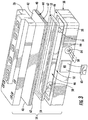
- FIG. 3 illustrates an exploded view of an integrated power semiconductor package 34 that can have the base plate 40 integrated with the cooling structure 38 by applying an adhesive 52 as a sealant, instead of a compressive O-ring of an open structure, thereby avoiding the need for screws and clearance between the base plate 40 and the cooling structure cavity 46.
- the a base plate 40 can have a first surface 42 and an opposing second surface 44 with at least one power semiconductor module 36 mounted to the first surface 42.
- a cooling structure 38 can have at least one cavity 46 for containing a cooling liquid 58 therein, and a contact rim 48 arranged around a perimeter of the cavity 46.
- the cavity 46 can have an inlet 54 and an outlet 56 for circulating the cooling liquid 58 inside the cavity 46.
- the inlet 54 and the outlet 56 can be positioned concentric with each other such that cooling liquid 58 flows into the cavity 46 through an inner port 64 and counter-flows out of the cavity in an outer annular port 66 positioned concentric with the inner port 64.
- the cooling structure 38 can have a flow distributing element 62 in fluid communication with the cooling liquid 58 in the cavity 46 for maintaining proper cooling liquid 58 flow distribution along the second surface 44 of the base plate 40 and to maximize heat transfer from the base plate 40. Cooling fins and other heat transfer surface extensions can extend from the base plate 40 to enhance heat transfer.
- a contact rim 48 can be arranged around a perimeter of the cavity 46 and configured to receive an adhesive 52.
- the contact rim 48 can be affixed parallel to and abutting against the second surface 44 of the base plate 40 thereby forming a hermetic seal at the adhesive 52.
- the hermetic seal is defined herein as meeting Military Standard 883; Test Method 1014.
- adhesive 52 as the sealing mechanism permits any appropriate material to be used for the cooling structure 38.
- a flow meter 60 can be attached to the cooling structure cavity 46.
- a non-limiting example of a flow meter 60 is a strain gauge to measure the amount of cavity deflection caused by cooling liquid 58 flowing through the cooling structure 38, and then correlate the amount of cavity deflection to a specific cooling liquid 58 flow rate.
- the strain gage flow meter 60 can also be used to detect coolant flow distribution problems in the power semiconductor package 34 integrated structure. It should be appreciated that any type of flow meter 60 can be applied in the semiconductor package 34 to measure the cooling liquid 58 flow rate.
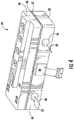
- FIG. 4 illustrates an assembled view of an exemplary closed or integrated power semiconductor package 34 showing the base plate 40 integrated with the cooling structure 38 by applying an adhesive 52 as a sealant.
- a cooling structure 38 can have at least one cavity 46 for containing a cooling liquid 58 therein, and a contact rim 48 arranged around a perimeter of the cavity 46.
- the cavity 46 can have an inlet 54 and an outlet 56 for circulating the cooling liquid 58 inside the cavity 46.
- the cooling structure 38 can have a flow distributing element (not shown) in contact with the cooling liquid 58 in the cavity 46 for maintaining proper cooling liquid 58 flow distribution along the base plate 40.
- Adhesive 52 bonding of the baseplate 40 substrate with the cooling structure 38 substrate can be difficult because each substrate can have different coefficients of thermal expansion (CTE). Additionally, stresses caused by temperature extremes in service and thermal cycling of the semiconductor package 34 sometimes makes a difficult situation more complicated.
- Adhesives 52 can be selected with CTE's as close as possible to the materials being bonded. Or, a more flexible and toughened adhesive can be applied to compensate for the CTE mismatch between the baseplate 40 and the cooling structure 38.
- the baseplate 40 can be a metal and the cooling structure 38 can be a plastic. Consideration of service conditions, shrink rates, and substrate material CTE mismatches is necessary for proper adhesive 52 selection.
- the adhesive 52 can be, for example, Master Bond EP30LTE, having linear CTE in the range of about 8.0 to about 10.0 micro-inches/inch-°F.
- Scotch-Weld Adhesive 2214 as manufactured by 3M is a suitable adhesive 52 for bonding the power semiconductor packages 34.
- the operating temperature range of the Scotch-Weld adhesive 52 can be about -60°F to about +250°F, and the linear CTE for the Scotch-Weld adhesive 52 can be about 24.0 to about 75 micro-inches/inch-°F.
- the adhesive 52 can be applied as a continuous bead on the flat surface 50 of the contact rim 48 thereby making the adhesive 52 a contiguous seal to prevent coolant leakage thorough many operating cycles.
- the adhesive 52 seal is located outside of the heat conductive path between the base plate 40 and the cooling liquid 58. Thus, the cooling performance of the semiconductor package 34 is not sensitive to the thermal conductivity properties of the adhesive 52.
- the cooling structure 38 can be constructed from a rigid material such as metal or flexible materials such as molded flexible plastic, fiber reinforced plastic, composites, rubber compounds and combinations thereof.
- a flow meter 60 such as a strain gauge, can be arranged with the cavity 46 to detect cooling liquid 58 flow rate in the cavity 46.
- the flow distributing element 62 can have micro-channels for proper distribution of the cooling liquid 58.
- an embodiment of the semiconductor package 34 with a six cooling structures 38 and six cavities 46 for receiving six semiconductor modules 36.
- a cooling structure may have common inlet 54 and outlet 56 extending between each cavity 46 for the cooling liquid 58.
- the semiconductor modules 36 may contain semiconductor devices such as insulated gate bipolar transistors (IGBTs), metal oxide semiconductor field effect transistors (MOSFETs), bipolar junction transistors (BJTs), integrated gate-commutated thyristors (IGCTs), gate turn-off (GTO) thyristors, Silicon Controlled Rectifiers (SCRs), diodes and combinations thereof.
- the devices can be constructed from materials such as Silicon (Si), Silicon Carbide (SiC), Gallium Nitride (GaN), Gallium Arsenide (GaAs), and combinations thereof.
- a method for attaching and sealing a semiconductor cooling structure 38 in a semiconductor package 34 can have the steps of: identifying a base plate 40 of a semiconductor package 34, the base plate 40 comprising a first surface 42 and an opposing second surface 44; mounting at least one power semiconductor module 36 to the first surface 42 of the base plate 40; matching a cooling structure 38 to the base plate 40, the cooling structure 38 comprising at least one cavity 46 for containing a cooling liquid 58 therein; preparing a contact rim 48 arranged around a perimeter of the cavity 46, the contact rim 48 configured to receive an adhesive 52; and affixing the contact rim 48 parallel to and abutting against the second surface 44 of the base plate 40 thereby forming a hermetic seal at the adhesive 52.
- Additional method steps can include: mounting at least one flow meter 60 to the at least one cavity 46; measuring the amount of cavity 46 deflection caused by cooling liquid 58 flowing through the cooling structure 38, and correlating the amount of cavity deflection to a specific cooling liquid 58 flow rate.
Landscapes
- Engineering & Computer Science (AREA)
- Microelectronics & Electronic Packaging (AREA)
- Physics & Mathematics (AREA)
- Thermal Sciences (AREA)
- Power Engineering (AREA)
- Cooling Or The Like Of Semiconductors Or Solid State Devices (AREA)
Abstract
Description
- The present subject matter relates generally to wind turbines and, more particularly, to methods and devices for attaching and sealing a cooling structure onto power semiconductor modules to form semiconductor packages for power converters.
- Modern wind turbines are used to supply electricity into the electrical grid generally through a power converter that uses various power electronic systems. Semiconductor packages may be used to control power distribution to the various applications and devices of the power electronic system. A semiconductor package may generally include a number of semiconductor chips which function as current switches for relatively high voltage ranges. The semiconductors used in the package may have certain limitations, such as maximum breakdown voltage and current carrying capability. Due to the blocking voltage limitations of each individual semiconductor, several semiconductors may be connected in series to achieve the required voltage and to function in a higher power system. For example, insulated gate bipolar transistors (IGBTs) may have a relatively low voltage breakdown, and several IGBTs may be interconnected within a semiconductor package in parallel for high current capability and several IGBT packages could be connected in series in a stack to meet high voltage requirements, and hence allow switching in relatively high power applications. Furthermore, due to the need for high current in power electronic systems, semiconductor chips may also be arranged in sub-groups within a semiconductor package. For example, several groups of series-connected IGBTs may also be arranged in parallel in the package.
- Semiconductor devices generate heat when placed in service. Many known heat removal systems for such semiconductors include a path for heat flow with a high thermal resistance, thereby resulting in a high operating junction temperature for a particular amount of power loss in the semiconductor device. For example, the cooling path for many IGBT modules includes a semiconductor die soldered onto one side of an electrically-isolating substrate, e.g., aluminum nitride, thereby forming an electrical junction thereon. Most of the heat generated by the IGBT is channeled from the junction side of the electrically-isolating substrate, through the substrate, to the opposite side. Many such known substrates include a heat transfer mechanism on the side opposite the junction. This heat transfer mechanism is typically referred to as single-side cooling structure.
- Some large power semiconductors often consist of a high number of silicon chips or dies connected in series or parallel, depending on the use, and may be attached to a common board. Such large power semiconductors are often called power modules. Liquid cooling of power modules often involves having a cooling structure attached to the bottom, i.e. the base plate of the module. The cooling structure contains a closed circuit for a liquid coolant that may include inlet(s) and outlet(s) for providing fluid connections to a heat exchanger. This method is known as indirect cooling.
- Direct cooling of power semiconductor modules is also practiced, and involves a chamber for the liquid coolant defined in a cavity of the cooling structure. The base plate of the power semiconductor module may be attached to the cooling structure over the cavity, effectively acting as a lid to cover the cavity and placing the coolant in the cavity in thermal contact with the base plate for heat removal therefrom. Fasteners, such as bolts are screws, are often used to secure the cooling structure and base plate. The actual flow and/or heat transfer of the liquid coolant can be made in many different ways. One way is by using a distributing element, which is inserted in the cavity, and another known way is by having an array of cooling fins protruding from the base plate into the liquid coolant.
- Various aspects and advantages of the invention will be set forth in part in the following description, or may be clear from the description, or may be learned through practice of the invention.
- In one aspect, a power semiconductor package is disclosed having a base plate with a first surface and an opposing second surface. At least one power semiconductor module can be mounted to the first surface of the base plate. A cooling structure having at least one cavity for containing a cooling liquid therein is disclosed. A contact rim is arranged around a perimeter of the cavity and configured to receive an adhesive. The contact rim is affixed parallel to and abutting against the second surface of the base plate thereby forming a hermetic seal at the adhesive.
- In another aspect, a power converter is disclosed having at least one DC capacitor, and at least two three-phase bi-directional AC-DC converters, the AC-DC converters having at least one power semiconductor package described above.
- In another aspect, a method for attaching and sealing a semiconductor cooling structure in a semiconductor package is disclosed having the steps of: identifying a base plate of a semiconductor package, the base plate comprising a first surface and an opposing second surface; mounting at least one power semiconductor module to the first surface of the base plate; matching a cooling structure to the base plate, the cooling structure comprising at least one cavity for containing a cooling liquid therein; preparing a contact rim arranged around a perimeter of the cavity, the contact rim configured to receive an adhesive; and, affixing the contact rim parallel to and abutting against the second surface of the base plate thereby forming a hermetic seal at the adhesive.
- Various features, aspects and advantages of the present invention will become better understood with reference to the following description and appended claims. The accompanying drawings, which are incorporated in and constitute a part of this specification, illustrate embodiments of the invention and, together with the description, serve to explain the principles of the invention.
- In the drawings:
-
FIG. 1 illustrates a block diagram of an electronic system which may include power semiconductor packages in accordance with an embodiment of the present invention; -
FIG. 2 illustrates a prior art isometric of an open direct cooling heat sink with a gasket and power module; -
FIG. 3 illustrates an exploded view of the components of an exemplary closed or integrated power semiconductor package; -
FIG. 4 illustrates an assembled view of an exemplary closed or integrated power semiconductor package; -
FIG. 5 illustrates a closed power semiconductor package with room for six power semiconductor modules fitted to a direct cooled cooling structure; -
FIG. 6 illustrates a section cut through the closed power semiconductor package shown inFIG. 4 . - Repeat use of reference characters in the present specification and drawings is intended to represent the same or analogous features or elements of the present disclosure.
- Reference now will be made in detail to embodiments of the invention, one or more examples of which are illustrated in the drawings. Each example is provided by way of explanation of the invention, not limitation of the invention. In fact, it will be apparent to those skilled in the art that various modifications and variations can be made in the present invention without departing from the scope or spirit of the invention. For instance, features illustrated or described as part of one embodiment can be used with another embodiment to yield a still further embodiment. Thus, it is intended that the present invention covers such modifications and variations as come within the scope of the appended claims and their equivalents.
- In general, the present subject matter discloses devices for attaching and/or sealing a cooling plate to a semiconductor module using adhesive in place of fasteners and O-rings. These devices are useful when implementing a direct coolant to baseplate configuration where a cooling structure is affixed to the bottom of the semiconductor module. An issue that arises is the need to seal the contact rim of the cooling structure against the semiconductor module. Current practice is to provide an O-ring around the contact rim of the cooling structure and screw it to the base of the semiconductor module. An improved method disclosed herein uses an adhesive to bond and seal the cooling structure to the semiconductor module at the contact rim to make a power semiconductor integrated package thus removing a failure mode of coolant leakage at the O-ring. Cyclic temperature operations of the semiconductor module changes the ductility of the O-ring thereby causing the O-ring to become more rigid and fragile over time thus compromising the coolant seal. Using an adhesive in place of an O-ring removes a high-risk failure area of the sealed direct water cooled semiconductor integrated package. Also, by using an adhesive, the fasteners (screws) that hold the cooling structure to the semiconductor module can be eliminated. By utilizing adhesive in place of an O-ring and fasteners, fabrication can be more readily automated. Additive manufacturing can build a complete base plate and cooling structure that includes a flow distributing element. Discrete semiconductor components can then be mounted to the base plate to construct the semiconductor module. This would eliminate the need for affixing a cooling structure to the bottom of a semiconductor module.
-
FIG. 1 illustrates a block diagram of an electronic system which may includepower semiconductor packages 34 in accordance with a windpower converter system 10 embodiment of the present disclosure. The windpower converter system 10 may be suitable for capturing power from wind usingturbine blades 12 and converting the captured wind power into mechanical power, and the mechanical power into electrical power. Thesystem 10 may include agearbox 16 connected to theturbine rotor 14 of theturbine blades 12. Thegearbox 16 may adapt the relatively low speed of theturbine rotor 14 with the relatively high speed of agenerator 18. - The
generator 18 may convert the mechanical power into electrical power, and may be, for example, an induction generator or a synchronous generator. For example, thegenerator 18 illustrated inFIG. 1 may be a doubly fed induction generator (DFIG), which includes a rotor winding 20 and a stator winding 22. The stator winding 22 of thegenerator 18 may be connected to atransformer 28 which transfers electrical power through inductively coupled conductors to a suitable voltage level for anelectrical grid 30. Thegrid 30 may be an interconnected network which delivers electrical power to various other electrical devices or networks. The rotor winding 20 of thegenerator 18 may be connected to thegrid 30 byconverters - The
system 10 may include two three-phase AC-DC converters DC capacitor 32. Theconverter 24 connected to the rotor winding 20 of thegenerator 18 may be referred to as therotor side converter 24, while theconverter 26 connected to thegrid 30 by thetransformer 28 may be referred to as thegrid side converter 26. Thebidirectional converters grid 30 and may also increase power quality and angular stability and decrease the harmonic content introduced into the grid 30 (e.g., via filters). - The
converters converters system 10. For example, theconverters several semiconductor packages 34 such as insulated gate bipolar transistors (IGBTs). In some embodiments, theIGBTs 34, or any other transistors used in theconverters - It should be appreciated that
Fig. 1 illustrates a non-limiting embodiment of the invention. Power bridges made from semiconductor packages disclosed herein can be used in numerous applications including solar and automotive. In these cases, the illustratedDC capacitor 32 can be any DC source such as a battery or photovoltaic array and the 3-phase AC output might feed a power grid, motor, pump, light bulb or any other electrical load. - Direct liquid-cooling of power semiconductor packages 34 can further be categorized into an open structure, as seen in the prior art of
FIG. 2 , and a closed or integrated structure, as taught herein and shown inFIGS. 3 thru 6 .FIG. 2 illustrates a prior art open structure using a direct cooling heat sink 3 with itsbasin 4 and an inlet and/or outlet 6. A gasket or O-ring 7 is used as a seal and is inserted between the heat sink 3 and thepower module 2 containing a base plate 5. To ensure an even distribution of the liquid coolant, a flow distributing element 8 is inserted in thebasin 4. Thepower module 2 is screwed or bolted to the heat sink 3 by bolts or screws 9. Bending stresses caused by thepower module 2 mountingscrews 9 combined with the force exerted by agasket 7 and pressure pulses from the coolant on the baseplate can cause the semiconductor ceramic substrate material to crack, violating electrical insulation properties and destroying the device instantaneously. - Additionally, in the open structures of
FIG. 2 , it is often practical to use apower module 2 with a pre-bend base plate 5. When attaching a pre-bend base plate 5 to the heat sink 3 with a flat upper edge of thebasin 4, forces from the bolts orscrews 9, combined with agasket 7 acting as a fulcrum, will try to flatten out the pre-bent base plate 5 which will cause the semiconductor ceramic chip substrate to crack and result in isolation failure. Also, installing the fixing screws 9 is a time intensive process, usually conducted by hand, requiring skilled labor for proper torqueing. If fins or other heat transfer enhancements are used to extend the surface area of the base plate 5, a clearance is provided between the fin tips and theheat sink basin 4 to allow for travel distance during O-ring compression and sealing. - An effective solution to these problems is a closed or integrated
power semiconductor package 34, as taught herein and illustrated inFIGS. 3 - 6 .FIG. 3 illustrates an exploded view of an integratedpower semiconductor package 34 that can have thebase plate 40 integrated with the coolingstructure 38 by applying an adhesive 52 as a sealant, instead of a compressive O-ring of an open structure, thereby avoiding the need for screws and clearance between thebase plate 40 and thecooling structure cavity 46. The abase plate 40 can have afirst surface 42 and an opposingsecond surface 44 with at least onepower semiconductor module 36 mounted to thefirst surface 42. A coolingstructure 38 can have at least onecavity 46 for containing a coolingliquid 58 therein, and acontact rim 48 arranged around a perimeter of thecavity 46. Thecavity 46 can have aninlet 54 and anoutlet 56 for circulating the coolingliquid 58 inside thecavity 46. Theinlet 54 and theoutlet 56 can be positioned concentric with each other such that cooling liquid 58 flows into thecavity 46 through aninner port 64 and counter-flows out of the cavity in an outerannular port 66 positioned concentric with theinner port 64. The coolingstructure 38 can have aflow distributing element 62 in fluid communication with the coolingliquid 58 in thecavity 46 for maintainingproper cooling liquid 58 flow distribution along thesecond surface 44 of thebase plate 40 and to maximize heat transfer from thebase plate 40. Cooling fins and other heat transfer surface extensions can extend from thebase plate 40 to enhance heat transfer. Acontact rim 48 can be arranged around a perimeter of thecavity 46 and configured to receive an adhesive 52. The contact rim 48 can be affixed parallel to and abutting against thesecond surface 44 of thebase plate 40 thereby forming a hermetic seal at the adhesive 52. The hermetic seal is defined herein as meeting Military Standard 883; Test Method 1014. Using adhesive 52 as the sealing mechanism permits any appropriate material to be used for the coolingstructure 38. - When using a
cavity 46 constructed from flexible material and the adhesive 52 sealant, aflow meter 60 can be attached to thecooling structure cavity 46. A non-limiting example of aflow meter 60 is a strain gauge to measure the amount of cavity deflection caused by coolingliquid 58 flowing through the coolingstructure 38, and then correlate the amount of cavity deflection to aspecific cooling liquid 58 flow rate. The straingage flow meter 60 can also be used to detect coolant flow distribution problems in thepower semiconductor package 34 integrated structure. It should be appreciated that any type offlow meter 60 can be applied in thesemiconductor package 34 to measure the coolingliquid 58 flow rate. -
FIG. 4 illustrates an assembled view of an exemplary closed or integratedpower semiconductor package 34 showing thebase plate 40 integrated with the coolingstructure 38 by applying an adhesive 52 as a sealant. A coolingstructure 38 can have at least onecavity 46 for containing a coolingliquid 58 therein, and acontact rim 48 arranged around a perimeter of thecavity 46. Thecavity 46 can have aninlet 54 and anoutlet 56 for circulating the coolingliquid 58 inside thecavity 46. The coolingstructure 38 can have a flow distributing element (not shown) in contact with the coolingliquid 58 in thecavity 46 for maintainingproper cooling liquid 58 flow distribution along thebase plate 40. -
Adhesive 52 bonding of thebaseplate 40 substrate with the coolingstructure 38 substrate can be difficult because each substrate can have different coefficients of thermal expansion (CTE). Additionally, stresses caused by temperature extremes in service and thermal cycling of thesemiconductor package 34 sometimes makes a difficult situation more complicated.Adhesives 52 can be selected with CTE's as close as possible to the materials being bonded. Or, a more flexible and toughened adhesive can be applied to compensate for the CTE mismatch between thebaseplate 40 and the coolingstructure 38. For example, thebaseplate 40 can be a metal and the coolingstructure 38 can be a plastic. Consideration of service conditions, shrink rates, and substrate material CTE mismatches is necessary for proper adhesive 52 selection. - When low shrinkage, low thermal expansion and dimensional stability is required, the adhesive 52 can be, for example, Master Bond EP30LTE, having linear CTE in the range of about 8.0 to about 10.0 micro-inches/inch-°F. For other applications, Scotch-Weld Adhesive 2214 as manufactured by 3M is a
suitable adhesive 52 for bonding the power semiconductor packages 34. The operating temperature range of the Scotch-Weld adhesive 52 can be about -60°F to about +250°F, and the linear CTE for the Scotch-Weld adhesive 52 can be about 24.0 to about 75 micro-inches/inch-°F. The adhesive 52 can be applied as a continuous bead on theflat surface 50 of thecontact rim 48 thereby making the adhesive 52 a contiguous seal to prevent coolant leakage thorough many operating cycles. The adhesive 52 seal is located outside of the heat conductive path between thebase plate 40 and the coolingliquid 58. Thus, the cooling performance of thesemiconductor package 34 is not sensitive to the thermal conductivity properties of the adhesive 52. - The cooling
structure 38 can be constructed from a rigid material such as metal or flexible materials such as molded flexible plastic, fiber reinforced plastic, composites, rubber compounds and combinations thereof. Using aflexible cooling structure 38, aflow meter 60, such as a strain gauge, can be arranged with thecavity 46 to detect cooling liquid 58 flow rate in thecavity 46. Additionally, theflow distributing element 62 can have micro-channels for proper distribution of the coolingliquid 58. - As illustrated in
FIG. 5 , an embodiment of thesemiconductor package 34 with a sixcooling structures 38 and sixcavities 46 for receiving sixsemiconductor modules 36. Such a cooling structure may havecommon inlet 54 andoutlet 56 extending between eachcavity 46 for the coolingliquid 58. Thesemiconductor modules 36 may contain semiconductor devices such as insulated gate bipolar transistors (IGBTs), metal oxide semiconductor field effect transistors (MOSFETs), bipolar junction transistors (BJTs), integrated gate-commutated thyristors (IGCTs), gate turn-off (GTO) thyristors, Silicon Controlled Rectifiers (SCRs), diodes and combinations thereof. The devices can be constructed from materials such as Silicon (Si), Silicon Carbide (SiC), Gallium Nitride (GaN), Gallium Arsenide (GaAs), and combinations thereof. -
FIG. 6 illustrates a section cut through the closedpower semiconductor package 34 as shown inFIG. 4 having thebase plate 40 integrated with the coolingstructure 38 by applying an adhesive 52 as a sealant. A coolingstructure 38 can have at least onecavity 46 for containing a coolingliquid 58 therein. Thecavity 46 can have aninlet 54 and anoutlet 56 for circulating the coolingliquid 58 inside thecavity 46. - A method for attaching and sealing a
semiconductor cooling structure 38 in asemiconductor package 34 can have the steps of: identifying abase plate 40 of asemiconductor package 34, thebase plate 40 comprising afirst surface 42 and an opposingsecond surface 44; mounting at least onepower semiconductor module 36 to thefirst surface 42 of thebase plate 40; matching acooling structure 38 to thebase plate 40, the coolingstructure 38 comprising at least onecavity 46 for containing a coolingliquid 58 therein; preparing acontact rim 48 arranged around a perimeter of thecavity 46, thecontact rim 48 configured to receive an adhesive 52; and affixing thecontact rim 48 parallel to and abutting against thesecond surface 44 of thebase plate 40 thereby forming a hermetic seal at the adhesive 52. Additional method steps can include: mounting at least oneflow meter 60 to the at least onecavity 46; measuring the amount ofcavity 46 deflection caused by coolingliquid 58 flowing through the coolingstructure 38, and correlating the amount of cavity deflection to aspecific cooling liquid 58 flow rate. - This written description uses examples to disclose the invention, including the preferred mode, and also to enable any person skilled in the art to practice the invention, including making and using any devices or systems and performing any incorporated methods. The patentable scope of the invention is defined by the claims, and may include other examples that occur to those skilled in the art. Such other examples are intended to be within the scope of the claims if they include structural elements that do not differ from the literal language of the claims, or if they include equivalent structural elements with insubstantial differences from the literal languages of the claims.
- Various aspects and embodiments of the present invention are defined by the following numbered clauses:
- 1. A power semiconductor package, comprising:
- a base plate comprising a first surface and an opposing second surface;
- at least one power semiconductor module mounted to the first surface of the base plate;
- a cooling structure comprising at least one cavity for containing a cooling liquid therein, wherein a contact rim is arranged around a perimeter of the cavity and configured to receive an adhesive, the contact rim affixed parallel to and abutting against the second surface of the base plate thereby forming a hermetic seal at the adhesive.
- 2. The power semiconductor package of clause 1, wherein the cavity comprises an inlet and an outlet for circulating the cooling liquid.
- 3. The power semiconductor package of any preceding clause, wherein the coefficient of thermal expansion of the adhesive is in the range of about 8.0 to about 75.0 micro-inches/inch-°F.
- 4. The power semiconductor package of any preceding clause, wherein the cooling structure is flexible.
- 5. The power semiconductor package of any preceding clause, further comprising at least one flow meter arranged with the cavity.
- 6. The power semiconductor package of any preceding clause, wherein the cooling structure comprises at least two cavities.
- 7. The power semiconductor package of any preceding clause, wherein the cooling structure is constructed of at least one of metal, molded plastic, fiber reinforced plastic, composites, and combinations thereof.
- 8. The power semiconductor package of any preceding clause, wherein the cooling structure further comprises a flow distributing element in fluid communication with the cooling liquid.
- 9. The power semiconductor package of any preceding clause, wherein the semiconductor package is a closed or integrated structure.
- 10. A power converter, comprising;
- at least one DC capacitor, and,
- at least two three-phase bi-directional AC-DC converters, the AC-DC converters comprising at least one power semiconductor package, the at least one power semiconductor package comprising:
- a base plate comprising a first surface and an opposing second surface;
- at least one power semiconductor module mounted to the first surface of the base plate;
- a cooling structure comprising at least one cavity for containing a cooling liquid therein, wherein a contact rim is arranged around a perimeter of the cavity and configured to receive an adhesive, the contact rim affixed parallel to and abutting against the second surface of the base plate thereby forming a hermetic seal at the adhesive; and,
- wherein the semiconductor package is a closed or integrated structure.
- 11. The power converter of
clause 10, wherein the cavity comprises an inlet and an outlet for circulating the cooling liquid. - 12. The power converter of any preceding clause, wherein the coefficient of thermal expansion of the adhesive is in the range of about 8.0 to about 75.0 microinches/inch-°F.
- 13. The power converter of any preceding clause, wherein the cooling structure is flexible.
- 14. The power converter of any preceding clause, further comprising at least one flow meter arranged with the cavity.
- 15. The power converter of any preceding clause, wherein the cooling structure comprises at least two cavities.
- 16. The power converter of any preceding clause, wherein the cooling structure is constructed of at least one of metal, molded plastic, fiber reinforced plastic, composites, and combinations thereof.
- 17. The power converter of any preceding clause, wherein the cooling structure further comprises a flow distributing element in fluid communication with the cooling liquid.
- 18. A method for attaching and sealing a semiconductor cooling structure in a semiconductor package, comprising:
- identifying a base plate of a semiconductor package, the base plate comprising a first surface and an opposing second surface;
- mounting at least one power semiconductor module to the first surface of the base plate;
- matching a cooling structure to the base plate, the cooling structure comprising at least one cavity for containing a cooling liquid therein;
- preparing a contact rim arranged around a perimeter of the cavity, the contact rim configured to receive an adhesive; and,
- affixing the contact rim parallel to and abutting against the second surface of the base plate thereby forming a hermetic seal at the adhesive.
- 19. The method of
clause 18, wherein the semiconductor package is a closed or integrated structure. - 20. The method of any preceding clause, further comprising:
- mounting at least one flow meter to the at least one cavity;
- measuring the amount of cavity deflection caused by cooling liquid flowing through the cooling structure; and
- correlating the amount of cavity deflection to a specific cooling liquid flow rate.
Claims (10)
- A power semiconductor package (34), comprising:a base plate (40) comprising a first surface (42) and an opposing second surface (44);at least one power semiconductor module (36) mounted to the first surface (42) of the base plate (40);a cooling structure (38) comprising at least one cavity (46) for containing a cooling liquid (58) therein, wherein a contact rim (48) is arranged around a perimeter of the cavity (46) and configured to receive an adhesive (52), the contact rim (48) affixed parallel to and abutting against the second surface (44) of the base plate (40) thereby forming a hermetic seal at the adhesive (52).
- The power semiconductor package (34) of claim 1, wherein the cavity (46) comprises an inlet (54) and an outlet (56) for circulating the cooling liquid (58).
- The power semiconductor package of any preceding claim, wherein the coefficient of thermal expansion of the adhesive (52) is in the range of about 8.0 to about 75.0 micro-inches/inch-°F.
- The power semiconductor package (34) of any preceding claim, wherein the cooling structure (38) is flexible and comprises at least one flow meter (60) arranged with the cavity (46).
- The power semiconductor package (34) of any preceding claim, wherein the cooling structure (38) further comprises a flow distributing element (62) in fluid communication with the cooling liquid (58).
- The power semiconductor package (34) of any preceding claim, wherein the semiconductor package (34) is a closed or integrated structure.
- A power converter (10), comprising;at least one DC capacitor (32), and,at least two three-phase bi-directional AC-DC converters (24, 26), the AC-DC converters (24, 26) comprising at least one power semiconductor package (34), the at least one power semiconductor package (34) comprising:wherein the semiconductor package (34) is a closed or integrated structure.a base plate (40) comprising a first surface (42) and an opposing second surface (44);at least one power semiconductor module (36) mounted to the first surface (42) of the base plate (40); and,a cooling structure (38) comprising at least one cavity (46) for containing a cooling liquid (58) therein, wherein a contact rim (48) is arranged around a perimeter of the cavity (46) and configured to receive an adhesive (52), the contact rim (48) affixed parallel to and abutting against the second surface (44) of the base plate (40) thereby forming a hermetic seal at the adhesive (52);
- The power converter (10) of claim 7, wherein the coefficient of thermal expansion of the adhesive (52) is in the range of about 8.0 to about 75.0 microinches/inch-°F.
- The power converter (10) of claim 7 or 8, wherein the cooling structure (38) is flexible and comprises at least one flow meter (60) arranged with the cavity (46).
- The power converter (10) of claim 7, 8 or 9, wherein the cooling structure (38) further comprises a flow distributing element (62) in fluid communication with the cooling liquid (58).
Applications Claiming Priority (1)
| Application Number | Priority Date | Filing Date | Title |
|---|---|---|---|
| US15/713,759 US20190096787A1 (en) | 2017-09-25 | 2017-09-25 | Methods and Devices for Attaching and Sealing a Semiconductor Cooling Structure |
Publications (2)
| Publication Number | Publication Date |
|---|---|
| EP3460840A1 true EP3460840A1 (en) | 2019-03-27 |
| EP3460840B1 EP3460840B1 (en) | 2020-05-20 |
Family
ID=63685590
Family Applications (1)
| Application Number | Title | Priority Date | Filing Date |
|---|---|---|---|
| EP18195876.0A Active EP3460840B1 (en) | 2017-09-25 | 2018-09-21 | Devices for attaching and sealing a semiconductor cooling structure |
Country Status (4)
| Country | Link |
|---|---|
| US (1) | US20190096787A1 (en) |
| EP (1) | EP3460840B1 (en) |
| DK (1) | DK3460840T3 (en) |
| ES (1) | ES2809229T3 (en) |
Families Citing this family (4)
| Publication number | Priority date | Publication date | Assignee | Title |
|---|---|---|---|---|
| JP2019033624A (en) * | 2017-08-09 | 2019-02-28 | 株式会社デンソー | Power converter |
| EP4009364B8 (en) | 2020-12-03 | 2023-12-06 | Hitachi Energy Ltd | Arrangement of a power semiconductor module and a cooler |
| CN113437037B (en) * | 2021-06-29 | 2024-05-24 | 中创杜菲(北京)汽车科技有限公司 | Power semiconductor package cooling device |
| CN117238870B (en) * | 2023-11-15 | 2024-01-30 | 中国海洋大学 | An active refrigeration device for chip heat dissipation |
Citations (4)
| Publication number | Priority date | Publication date | Assignee | Title |
|---|---|---|---|---|
| US20100232112A1 (en) * | 2009-03-12 | 2010-09-16 | Aisin Aw Co., Ltd. | Semiconductor module |
| US20130215573A1 (en) * | 2012-02-16 | 2013-08-22 | Jon Wagner | Motor control device |
| US20160118317A1 (en) * | 2014-10-27 | 2016-04-28 | Ebullient, Llc | Microprocessor assembly adapted for fluid cooling |
| EP3086454A1 (en) * | 2015-04-22 | 2016-10-26 | GE Energy Power Conversion Technology Ltd | Improving life of a semiconductor by reducing temperature changes therein via reactive power |
-
2017
- 2017-09-25 US US15/713,759 patent/US20190096787A1/en not_active Abandoned
-
2018
- 2018-09-21 EP EP18195876.0A patent/EP3460840B1/en active Active
- 2018-09-21 ES ES18195876T patent/ES2809229T3/en active Active
- 2018-09-21 DK DK18195876.0T patent/DK3460840T3/en active
Patent Citations (4)
| Publication number | Priority date | Publication date | Assignee | Title |
|---|---|---|---|---|
| US20100232112A1 (en) * | 2009-03-12 | 2010-09-16 | Aisin Aw Co., Ltd. | Semiconductor module |
| US20130215573A1 (en) * | 2012-02-16 | 2013-08-22 | Jon Wagner | Motor control device |
| US20160118317A1 (en) * | 2014-10-27 | 2016-04-28 | Ebullient, Llc | Microprocessor assembly adapted for fluid cooling |
| EP3086454A1 (en) * | 2015-04-22 | 2016-10-26 | GE Energy Power Conversion Technology Ltd | Improving life of a semiconductor by reducing temperature changes therein via reactive power |
Also Published As
| Publication number | Publication date |
|---|---|
| US20190096787A1 (en) | 2019-03-28 |
| EP3460840B1 (en) | 2020-05-20 |
| DK3460840T3 (en) | 2020-08-24 |
| ES2809229T3 (en) | 2021-03-03 |
Similar Documents
| Publication | Publication Date | Title |
|---|---|---|
| EP3460840B1 (en) | Devices for attaching and sealing a semiconductor cooling structure | |
| Abebe et al. | Integrated motor drives: state of the art and future trends | |
| US10186470B2 (en) | Heat sink for cooling of power semiconductor modules | |
| US10798854B2 (en) | Modular power module with integrated coolant passageway and assemblies thereof | |
| US12316238B2 (en) | Air-cooled power converter | |
| US8531027B2 (en) | Press-pack module with power overlay interconnection | |
| JP7091878B2 (en) | Power modules, power converters, and methods for manufacturing power modules | |
| EP3026701B1 (en) | Power module and manufacturing method thereof | |
| US10468314B2 (en) | Semiconductor power module and power conversion apparatus | |
| US20190304866A1 (en) | Semiconductor apparatus, method for manufacturing the same and electric power conversion device | |
| Lasserre et al. | Integrated Bi-directional SiC MOSFET power switches for efficient, power dense and reliable matrix converter assembly | |
| CN109860159B (en) | Semiconductor module, method for manufacturing the same, and power conversion device | |
| WO2019043950A1 (en) | SEMICONDUCTOR MODULE AND ENERGY CONVERTING DEVICE | |
| US11545874B2 (en) | Thermal management assemblies for electronic assemblies circumferentially mounted around a motor using a flexible substrate | |
| EP3288164B1 (en) | Power conversion device | |
| EP3096351A1 (en) | Thermal interface foil | |
| Nashida et al. | All-SiC Module for Mega-Solar Power Conditioner | |
| Lee et al. | New PFC-integrated intelligent power module for home appliances | |
| US20250079271A1 (en) | Semiconductor device, power converter, and method of manufacturing semiconductor device | |
| EP4272251B1 (en) | Power device and method for assembling a power device | |
| US11887904B2 (en) | Integrally bonded semiconductor device and power converter including the same | |
| US20240422914A1 (en) | Semiconductor device, power conversion device, and method of manufacturing semiconductor device | |
| Abu-Zama et al. | Mechanical Design Considerations for Electric Vehicle Power Electronics | |
| Reynes et al. | Thermal management optimization of a 5 MW power electronic converter | |
| WO2021033270A1 (en) | Semiconductor device, electric power converter and moving body |
Legal Events
| Date | Code | Title | Description |
|---|---|---|---|
| PUAI | Public reference made under article 153(3) epc to a published international application that has entered the european phase |
Free format text: ORIGINAL CODE: 0009012 |
|
| STAA | Information on the status of an ep patent application or granted ep patent |
Free format text: STATUS: THE APPLICATION HAS BEEN PUBLISHED |
|
| AK | Designated contracting states |
Kind code of ref document: A1 Designated state(s): AL AT BE BG CH CY CZ DE DK EE ES FI FR GB GR HR HU IE IS IT LI LT LU LV MC MK MT NL NO PL PT RO RS SE SI SK SM TR |
|
| AX | Request for extension of the european patent |
Extension state: BA ME |
|
| STAA | Information on the status of an ep patent application or granted ep patent |
Free format text: STATUS: REQUEST FOR EXAMINATION WAS MADE |
|
| 17P | Request for examination filed |
Effective date: 20190925 |
|
| RBV | Designated contracting states (corrected) |
Designated state(s): AL AT BE BG CH CY CZ DE DK EE ES FI FR GB GR HR HU IE IS IT LI LT LU LV MC MK MT NL NO PL PT RO RS SE SI SK SM TR |
|
| GRAP | Despatch of communication of intention to grant a patent |
Free format text: ORIGINAL CODE: EPIDOSNIGR1 |
|
| STAA | Information on the status of an ep patent application or granted ep patent |
Free format text: STATUS: GRANT OF PATENT IS INTENDED |
|
| INTG | Intention to grant announced |
Effective date: 20191206 |
|
| GRAS | Grant fee paid |
Free format text: ORIGINAL CODE: EPIDOSNIGR3 |
|
| GRAA | (expected) grant |
Free format text: ORIGINAL CODE: 0009210 |
|
| STAA | Information on the status of an ep patent application or granted ep patent |
Free format text: STATUS: THE PATENT HAS BEEN GRANTED |
|
| AK | Designated contracting states |
Kind code of ref document: B1 Designated state(s): AL AT BE BG CH CY CZ DE DK EE ES FI FR GB GR HR HU IE IS IT LI LT LU LV MC MK MT NL NO PL PT RO RS SE SI SK SM TR |
|
| REG | Reference to a national code |
Ref country code: GB Ref legal event code: FG4D |
|
| REG | Reference to a national code |
Ref country code: CH Ref legal event code: EP |
|
| REG | Reference to a national code |
Ref country code: DE Ref legal event code: R096 Ref document number: 602018004747 Country of ref document: DE |
|
| REG | Reference to a national code |
Ref country code: AT Ref legal event code: REF Ref document number: 1273177 Country of ref document: AT Kind code of ref document: T Effective date: 20200615 |
|
| REG | Reference to a national code |
Ref country code: DK Ref legal event code: T3 Effective date: 20200820 |
|
| REG | Reference to a national code |
Ref country code: LT Ref legal event code: MG4D |
|
| REG | Reference to a national code |
Ref country code: NL Ref legal event code: MP Effective date: 20200520 |
|
| PG25 | Lapsed in a contracting state [announced via postgrant information from national office to epo] |
Ref country code: FI Free format text: LAPSE BECAUSE OF FAILURE TO SUBMIT A TRANSLATION OF THE DESCRIPTION OR TO PAY THE FEE WITHIN THE PRESCRIBED TIME-LIMIT Effective date: 20200520 Ref country code: LT Free format text: LAPSE BECAUSE OF FAILURE TO SUBMIT A TRANSLATION OF THE DESCRIPTION OR TO PAY THE FEE WITHIN THE PRESCRIBED TIME-LIMIT Effective date: 20200520 Ref country code: SE Free format text: LAPSE BECAUSE OF FAILURE TO SUBMIT A TRANSLATION OF THE DESCRIPTION OR TO PAY THE FEE WITHIN THE PRESCRIBED TIME-LIMIT Effective date: 20200520 Ref country code: GR Free format text: LAPSE BECAUSE OF FAILURE TO SUBMIT A TRANSLATION OF THE DESCRIPTION OR TO PAY THE FEE WITHIN THE PRESCRIBED TIME-LIMIT Effective date: 20200821 Ref country code: IS Free format text: LAPSE BECAUSE OF FAILURE TO SUBMIT A TRANSLATION OF THE DESCRIPTION OR TO PAY THE FEE WITHIN THE PRESCRIBED TIME-LIMIT Effective date: 20200920 Ref country code: NO Free format text: LAPSE BECAUSE OF FAILURE TO SUBMIT A TRANSLATION OF THE DESCRIPTION OR TO PAY THE FEE WITHIN THE PRESCRIBED TIME-LIMIT Effective date: 20200820 Ref country code: PT Free format text: LAPSE BECAUSE OF FAILURE TO SUBMIT A TRANSLATION OF THE DESCRIPTION OR TO PAY THE FEE WITHIN THE PRESCRIBED TIME-LIMIT Effective date: 20200921 |
|
| PG25 | Lapsed in a contracting state [announced via postgrant information from national office to epo] |
Ref country code: HR Free format text: LAPSE BECAUSE OF FAILURE TO SUBMIT A TRANSLATION OF THE DESCRIPTION OR TO PAY THE FEE WITHIN THE PRESCRIBED TIME-LIMIT Effective date: 20200520 Ref country code: RS Free format text: LAPSE BECAUSE OF FAILURE TO SUBMIT A TRANSLATION OF THE DESCRIPTION OR TO PAY THE FEE WITHIN THE PRESCRIBED TIME-LIMIT Effective date: 20200520 Ref country code: LV Free format text: LAPSE BECAUSE OF FAILURE TO SUBMIT A TRANSLATION OF THE DESCRIPTION OR TO PAY THE FEE WITHIN THE PRESCRIBED TIME-LIMIT Effective date: 20200520 Ref country code: BG Free format text: LAPSE BECAUSE OF FAILURE TO SUBMIT A TRANSLATION OF THE DESCRIPTION OR TO PAY THE FEE WITHIN THE PRESCRIBED TIME-LIMIT Effective date: 20200820 |
|
| REG | Reference to a national code |
Ref country code: AT Ref legal event code: MK05 Ref document number: 1273177 Country of ref document: AT Kind code of ref document: T Effective date: 20200520 |
|
| PG25 | Lapsed in a contracting state [announced via postgrant information from national office to epo] |
Ref country code: AL Free format text: LAPSE BECAUSE OF FAILURE TO SUBMIT A TRANSLATION OF THE DESCRIPTION OR TO PAY THE FEE WITHIN THE PRESCRIBED TIME-LIMIT Effective date: 20200520 Ref country code: NL Free format text: LAPSE BECAUSE OF FAILURE TO SUBMIT A TRANSLATION OF THE DESCRIPTION OR TO PAY THE FEE WITHIN THE PRESCRIBED TIME-LIMIT Effective date: 20200520 |
|
| PG25 | Lapsed in a contracting state [announced via postgrant information from national office to epo] |
Ref country code: SM Free format text: LAPSE BECAUSE OF FAILURE TO SUBMIT A TRANSLATION OF THE DESCRIPTION OR TO PAY THE FEE WITHIN THE PRESCRIBED TIME-LIMIT Effective date: 20200520 Ref country code: EE Free format text: LAPSE BECAUSE OF FAILURE TO SUBMIT A TRANSLATION OF THE DESCRIPTION OR TO PAY THE FEE WITHIN THE PRESCRIBED TIME-LIMIT Effective date: 20200520 Ref country code: IT Free format text: LAPSE BECAUSE OF FAILURE TO SUBMIT A TRANSLATION OF THE DESCRIPTION OR TO PAY THE FEE WITHIN THE PRESCRIBED TIME-LIMIT Effective date: 20200520 Ref country code: AT Free format text: LAPSE BECAUSE OF FAILURE TO SUBMIT A TRANSLATION OF THE DESCRIPTION OR TO PAY THE FEE WITHIN THE PRESCRIBED TIME-LIMIT Effective date: 20200520 Ref country code: CZ Free format text: LAPSE BECAUSE OF FAILURE TO SUBMIT A TRANSLATION OF THE DESCRIPTION OR TO PAY THE FEE WITHIN THE PRESCRIBED TIME-LIMIT Effective date: 20200520 Ref country code: RO Free format text: LAPSE BECAUSE OF FAILURE TO SUBMIT A TRANSLATION OF THE DESCRIPTION OR TO PAY THE FEE WITHIN THE PRESCRIBED TIME-LIMIT Effective date: 20200520 |
|
| REG | Reference to a national code |
Ref country code: DE Ref legal event code: R097 Ref document number: 602018004747 Country of ref document: DE |
|
| PG25 | Lapsed in a contracting state [announced via postgrant information from national office to epo] |
Ref country code: PL Free format text: LAPSE BECAUSE OF FAILURE TO SUBMIT A TRANSLATION OF THE DESCRIPTION OR TO PAY THE FEE WITHIN THE PRESCRIBED TIME-LIMIT Effective date: 20200520 Ref country code: SK Free format text: LAPSE BECAUSE OF FAILURE TO SUBMIT A TRANSLATION OF THE DESCRIPTION OR TO PAY THE FEE WITHIN THE PRESCRIBED TIME-LIMIT Effective date: 20200520 |
|
| REG | Reference to a national code |
Ref country code: ES Ref legal event code: FG2A Ref document number: 2809229 Country of ref document: ES Kind code of ref document: T3 Effective date: 20210303 |
|
| PLBE | No opposition filed within time limit |
Free format text: ORIGINAL CODE: 0009261 |
|
| STAA | Information on the status of an ep patent application or granted ep patent |
Free format text: STATUS: NO OPPOSITION FILED WITHIN TIME LIMIT |
|
| 26N | No opposition filed |
Effective date: 20210223 |
|
| PG25 | Lapsed in a contracting state [announced via postgrant information from national office to epo] |
Ref country code: SI Free format text: LAPSE BECAUSE OF FAILURE TO SUBMIT A TRANSLATION OF THE DESCRIPTION OR TO PAY THE FEE WITHIN THE PRESCRIBED TIME-LIMIT Effective date: 20200520 |
|
| REG | Reference to a national code |
Ref country code: BE Ref legal event code: MM Effective date: 20200930 |
|
| PG25 | Lapsed in a contracting state [announced via postgrant information from national office to epo] |
Ref country code: LU Free format text: LAPSE BECAUSE OF NON-PAYMENT OF DUE FEES Effective date: 20200921 |
|
| PG25 | Lapsed in a contracting state [announced via postgrant information from national office to epo] |
Ref country code: FR Free format text: LAPSE BECAUSE OF NON-PAYMENT OF DUE FEES Effective date: 20200930 |
|
| PG25 | Lapsed in a contracting state [announced via postgrant information from national office to epo] |
Ref country code: BE Free format text: LAPSE BECAUSE OF NON-PAYMENT OF DUE FEES Effective date: 20200930 Ref country code: IE Free format text: LAPSE BECAUSE OF NON-PAYMENT OF DUE FEES Effective date: 20200921 |
|
| REG | Reference to a national code |
Ref country code: CH Ref legal event code: PL |
|
| PG25 | Lapsed in a contracting state [announced via postgrant information from national office to epo] |
Ref country code: TR Free format text: LAPSE BECAUSE OF FAILURE TO SUBMIT A TRANSLATION OF THE DESCRIPTION OR TO PAY THE FEE WITHIN THE PRESCRIBED TIME-LIMIT Effective date: 20200520 Ref country code: MT Free format text: LAPSE BECAUSE OF FAILURE TO SUBMIT A TRANSLATION OF THE DESCRIPTION OR TO PAY THE FEE WITHIN THE PRESCRIBED TIME-LIMIT Effective date: 20200520 Ref country code: CY Free format text: LAPSE BECAUSE OF FAILURE TO SUBMIT A TRANSLATION OF THE DESCRIPTION OR TO PAY THE FEE WITHIN THE PRESCRIBED TIME-LIMIT Effective date: 20200520 |
|
| PG25 | Lapsed in a contracting state [announced via postgrant information from national office to epo] |
Ref country code: MK Free format text: LAPSE BECAUSE OF FAILURE TO SUBMIT A TRANSLATION OF THE DESCRIPTION OR TO PAY THE FEE WITHIN THE PRESCRIBED TIME-LIMIT Effective date: 20200520 Ref country code: MC Free format text: LAPSE BECAUSE OF FAILURE TO SUBMIT A TRANSLATION OF THE DESCRIPTION OR TO PAY THE FEE WITHIN THE PRESCRIBED TIME-LIMIT Effective date: 20200520 |
|
| PG25 | Lapsed in a contracting state [announced via postgrant information from national office to epo] |
Ref country code: LI Free format text: LAPSE BECAUSE OF NON-PAYMENT OF DUE FEES Effective date: 20210930 Ref country code: CH Free format text: LAPSE BECAUSE OF NON-PAYMENT OF DUE FEES Effective date: 20210930 |
|
| GBPC | Gb: european patent ceased through non-payment of renewal fee |
Effective date: 20220921 |
|
| P01 | Opt-out of the competence of the unified patent court (upc) registered |
Effective date: 20230530 |
|
| PG25 | Lapsed in a contracting state [announced via postgrant information from national office to epo] |
Ref country code: GB Free format text: LAPSE BECAUSE OF NON-PAYMENT OF DUE FEES Effective date: 20220921 |
|
| REG | Reference to a national code |
Ref country code: DE Ref legal event code: R081 Ref document number: 602018004747 Country of ref document: DE Owner name: GENERAL ELECTRIC RENOVABLES ESPANA, S.L., ES Free format text: FORMER OWNER: GENERAL ELECTRIC COMPANY, SCHENECTADY, NY, US |
|
| REG | Reference to a national code |
Ref country code: ES Ref legal event code: PC2A Owner name: GENERAL ELECTRIC RENOVABLES ESPANA S.L. Effective date: 20240809 |
|
| PGFP | Annual fee paid to national office [announced via postgrant information from national office to epo] |
Ref country code: DE Payment date: 20250820 Year of fee payment: 8 Ref country code: DK Payment date: 20250820 Year of fee payment: 8 |
|
| REG | Reference to a national code |
Ref country code: DE Ref legal event code: R079 Ref document number: 602018004747 Country of ref document: DE Free format text: PREVIOUS MAIN CLASS: H01L0023400000 Ipc: H10W0040600000 |
|
| PGFP | Annual fee paid to national office [announced via postgrant information from national office to epo] |
Ref country code: ES Payment date: 20251001 Year of fee payment: 8 |