EP3460838A1 - Substrate for power modules - Google Patents
Substrate for power modules Download PDFInfo
- Publication number
- EP3460838A1 EP3460838A1 EP17799428.2A EP17799428A EP3460838A1 EP 3460838 A1 EP3460838 A1 EP 3460838A1 EP 17799428 A EP17799428 A EP 17799428A EP 3460838 A1 EP3460838 A1 EP 3460838A1
- Authority
- EP
- European Patent Office
- Prior art keywords
- layer
- ceramic substrate
- equal
- circuit
- face
- Prior art date
- Legal status (The legal status is an assumption and is not a legal conclusion. Google has not performed a legal analysis and makes no representation as to the accuracy of the status listed.)
- Granted
Links
Images




Classifications
-
- H—ELECTRICITY
- H10—SEMICONDUCTOR DEVICES; ELECTRIC SOLID-STATE DEVICES NOT OTHERWISE PROVIDED FOR
- H10W—GENERIC PACKAGES, INTERCONNECTIONS, CONNECTORS OR OTHER CONSTRUCTIONAL DETAILS OF DEVICES COVERED BY CLASS H10
- H10W70/00—Package substrates; Interposers; Redistribution layers [RDL]
- H10W70/60—Insulating or insulated package substrates; Interposers; Redistribution layers
- H10W70/67—Insulating or insulated package substrates; Interposers; Redistribution layers characterised by their insulating layers or insulating parts
- H10W70/68—Shapes or dispositions thereof
- H10W70/685—Shapes or dispositions thereof comprising multiple insulating layers
-
- B—PERFORMING OPERATIONS; TRANSPORTING
- B23—MACHINE TOOLS; METAL-WORKING NOT OTHERWISE PROVIDED FOR
- B23K—SOLDERING OR UNSOLDERING; WELDING; CLADDING OR PLATING BY SOLDERING OR WELDING; CUTTING BY APPLYING HEAT LOCALLY, e.g. FLAME CUTTING; WORKING BY LASER BEAM
- B23K35/00—Rods, electrodes, materials, or media, for use in soldering, welding, or cutting
- B23K35/22—Rods, electrodes, materials, or media, for use in soldering, welding, or cutting characterised by the composition or nature of the material
-
- C—CHEMISTRY; METALLURGY
- C04—CEMENTS; CONCRETE; ARTIFICIAL STONE; CERAMICS; REFRACTORIES
- C04B—LIME, MAGNESIA; SLAG; CEMENTS; COMPOSITIONS THEREOF, e.g. MORTARS, CONCRETE OR LIKE BUILDING MATERIALS; ARTIFICIAL STONE; CERAMICS; REFRACTORIES; TREATMENT OF NATURAL STONE
- C04B37/00—Joining burned ceramic articles with other burned ceramic articles or other articles by heating
- C04B37/02—Joining burned ceramic articles with other burned ceramic articles or other articles by heating with metallic articles
- C04B37/023—Joining burned ceramic articles with other burned ceramic articles or other articles by heating with metallic articles characterised by the interlayer used
- C04B37/026—Joining burned ceramic articles with other burned ceramic articles or other articles by heating with metallic articles characterised by the interlayer used consisting of metals or metal salts
-
- H—ELECTRICITY
- H05—ELECTRIC TECHNIQUES NOT OTHERWISE PROVIDED FOR
- H05K—PRINTED CIRCUITS; CASINGS OR CONSTRUCTIONAL DETAILS OF ELECTRIC APPARATUS; MANUFACTURE OF ASSEMBLAGES OF ELECTRICAL COMPONENTS
- H05K1/00—Printed circuits
- H05K1/02—Details
- H05K1/0296—Conductive pattern lay-out details not covered by sub groups H05K1/02 - H05K1/0295
- H05K1/0298—Multilayer circuits
-
- H—ELECTRICITY
- H05—ELECTRIC TECHNIQUES NOT OTHERWISE PROVIDED FOR
- H05K—PRINTED CIRCUITS; CASINGS OR CONSTRUCTIONAL DETAILS OF ELECTRIC APPARATUS; MANUFACTURE OF ASSEMBLAGES OF ELECTRICAL COMPONENTS
- H05K1/00—Printed circuits
- H05K1/02—Details
- H05K1/03—Use of materials for the substrate
-
- H—ELECTRICITY
- H05—ELECTRIC TECHNIQUES NOT OTHERWISE PROVIDED FOR
- H05K—PRINTED CIRCUITS; CASINGS OR CONSTRUCTIONAL DETAILS OF ELECTRIC APPARATUS; MANUFACTURE OF ASSEMBLAGES OF ELECTRICAL COMPONENTS
- H05K1/00—Printed circuits
- H05K1/02—Details
- H05K1/03—Use of materials for the substrate
- H05K1/0306—Inorganic insulating substrates, e.g. ceramic, glass
-
- H—ELECTRICITY
- H05—ELECTRIC TECHNIQUES NOT OTHERWISE PROVIDED FOR
- H05K—PRINTED CIRCUITS; CASINGS OR CONSTRUCTIONAL DETAILS OF ELECTRIC APPARATUS; MANUFACTURE OF ASSEMBLAGES OF ELECTRICAL COMPONENTS
- H05K3/00—Apparatus or processes for manufacturing printed circuits
- H05K3/38—Improvement of the adhesion between the insulating substrate and the metal
-
- H—ELECTRICITY
- H10—SEMICONDUCTOR DEVICES; ELECTRIC SOLID-STATE DEVICES NOT OTHERWISE PROVIDED FOR
- H10W—GENERIC PACKAGES, INTERCONNECTIONS, CONNECTORS OR OTHER CONSTRUCTIONAL DETAILS OF DEVICES COVERED BY CLASS H10
- H10W40/00—Arrangements for thermal protection or thermal control
- H10W40/10—Arrangements for heating
-
- H—ELECTRICITY
- H10—SEMICONDUCTOR DEVICES; ELECTRIC SOLID-STATE DEVICES NOT OTHERWISE PROVIDED FOR
- H10W—GENERIC PACKAGES, INTERCONNECTIONS, CONNECTORS OR OTHER CONSTRUCTIONAL DETAILS OF DEVICES COVERED BY CLASS H10
- H10W40/00—Arrangements for thermal protection or thermal control
- H10W40/20—Arrangements for cooling
- H10W40/25—Arrangements for cooling characterised by their materials
- H10W40/255—Arrangements for cooling characterised by their materials having a laminate or multilayered structure, e.g. direct bond copper [DBC] ceramic substrates
-
- H—ELECTRICITY
- H10—SEMICONDUCTOR DEVICES; ELECTRIC SOLID-STATE DEVICES NOT OTHERWISE PROVIDED FOR
- H10W—GENERIC PACKAGES, INTERCONNECTIONS, CONNECTORS OR OTHER CONSTRUCTIONAL DETAILS OF DEVICES COVERED BY CLASS H10
- H10W70/00—Package substrates; Interposers; Redistribution layers [RDL]
- H10W70/60—Insulating or insulated package substrates; Interposers; Redistribution layers
-
- H—ELECTRICITY
- H10—SEMICONDUCTOR DEVICES; ELECTRIC SOLID-STATE DEVICES NOT OTHERWISE PROVIDED FOR
- H10W—GENERIC PACKAGES, INTERCONNECTIONS, CONNECTORS OR OTHER CONSTRUCTIONAL DETAILS OF DEVICES COVERED BY CLASS H10
- H10W70/00—Package substrates; Interposers; Redistribution layers [RDL]
- H10W70/60—Insulating or insulated package substrates; Interposers; Redistribution layers
- H10W70/67—Insulating or insulated package substrates; Interposers; Redistribution layers characterised by their insulating layers or insulating parts
- H10W70/68—Shapes or dispositions thereof
-
- C—CHEMISTRY; METALLURGY
- C04—CEMENTS; CONCRETE; ARTIFICIAL STONE; CERAMICS; REFRACTORIES
- C04B—LIME, MAGNESIA; SLAG; CEMENTS; COMPOSITIONS THEREOF, e.g. MORTARS, CONCRETE OR LIKE BUILDING MATERIALS; ARTIFICIAL STONE; CERAMICS; REFRACTORIES; TREATMENT OF NATURAL STONE
- C04B2237/00—Aspects relating to ceramic laminates or to joining of ceramic articles with other articles by heating
- C04B2237/02—Aspects relating to interlayers, e.g. used to join ceramic articles with other articles by heating
- C04B2237/12—Metallic interlayers
- C04B2237/122—Metallic interlayers based on refractory metals
-
- C—CHEMISTRY; METALLURGY
- C04—CEMENTS; CONCRETE; ARTIFICIAL STONE; CERAMICS; REFRACTORIES
- C04B—LIME, MAGNESIA; SLAG; CEMENTS; COMPOSITIONS THEREOF, e.g. MORTARS, CONCRETE OR LIKE BUILDING MATERIALS; ARTIFICIAL STONE; CERAMICS; REFRACTORIES; TREATMENT OF NATURAL STONE
- C04B2237/00—Aspects relating to ceramic laminates or to joining of ceramic articles with other articles by heating
- C04B2237/02—Aspects relating to interlayers, e.g. used to join ceramic articles with other articles by heating
- C04B2237/12—Metallic interlayers
- C04B2237/124—Metallic interlayers based on copper
-
- C—CHEMISTRY; METALLURGY
- C04—CEMENTS; CONCRETE; ARTIFICIAL STONE; CERAMICS; REFRACTORIES
- C04B—LIME, MAGNESIA; SLAG; CEMENTS; COMPOSITIONS THEREOF, e.g. MORTARS, CONCRETE OR LIKE BUILDING MATERIALS; ARTIFICIAL STONE; CERAMICS; REFRACTORIES; TREATMENT OF NATURAL STONE
- C04B2237/00—Aspects relating to ceramic laminates or to joining of ceramic articles with other articles by heating
- C04B2237/30—Composition of layers of ceramic laminates or of ceramic or metallic articles to be joined by heating, e.g. Si substrates
- C04B2237/32—Ceramic
- C04B2237/36—Non-oxidic
- C04B2237/366—Aluminium nitride
-
- C—CHEMISTRY; METALLURGY
- C04—CEMENTS; CONCRETE; ARTIFICIAL STONE; CERAMICS; REFRACTORIES
- C04B—LIME, MAGNESIA; SLAG; CEMENTS; COMPOSITIONS THEREOF, e.g. MORTARS, CONCRETE OR LIKE BUILDING MATERIALS; ARTIFICIAL STONE; CERAMICS; REFRACTORIES; TREATMENT OF NATURAL STONE
- C04B2237/00—Aspects relating to ceramic laminates or to joining of ceramic articles with other articles by heating
- C04B2237/30—Composition of layers of ceramic laminates or of ceramic or metallic articles to be joined by heating, e.g. Si substrates
- C04B2237/32—Ceramic
- C04B2237/36—Non-oxidic
- C04B2237/368—Silicon nitride
-
- C—CHEMISTRY; METALLURGY
- C04—CEMENTS; CONCRETE; ARTIFICIAL STONE; CERAMICS; REFRACTORIES
- C04B—LIME, MAGNESIA; SLAG; CEMENTS; COMPOSITIONS THEREOF, e.g. MORTARS, CONCRETE OR LIKE BUILDING MATERIALS; ARTIFICIAL STONE; CERAMICS; REFRACTORIES; TREATMENT OF NATURAL STONE
- C04B2237/00—Aspects relating to ceramic laminates or to joining of ceramic articles with other articles by heating
- C04B2237/30—Composition of layers of ceramic laminates or of ceramic or metallic articles to be joined by heating, e.g. Si substrates
- C04B2237/40—Metallic
- C04B2237/407—Copper
-
- H—ELECTRICITY
- H10—SEMICONDUCTOR DEVICES; ELECTRIC SOLID-STATE DEVICES NOT OTHERWISE PROVIDED FOR
- H10W—GENERIC PACKAGES, INTERCONNECTIONS, CONNECTORS OR OTHER CONSTRUCTIONAL DETAILS OF DEVICES COVERED BY CLASS H10
- H10W40/00—Arrangements for thermal protection or thermal control
- H10W40/20—Arrangements for cooling
- H10W40/25—Arrangements for cooling characterised by their materials
- H10W40/259—Ceramics or glasses
-
- H—ELECTRICITY
- H10—SEMICONDUCTOR DEVICES; ELECTRIC SOLID-STATE DEVICES NOT OTHERWISE PROVIDED FOR
- H10W—GENERIC PACKAGES, INTERCONNECTIONS, CONNECTORS OR OTHER CONSTRUCTIONAL DETAILS OF DEVICES COVERED BY CLASS H10
- H10W90/00—Package configurations
- H10W90/701—Package configurations characterised by the relative positions of pads or connectors relative to package parts
- H10W90/731—Package configurations characterised by the relative positions of pads or connectors relative to package parts of die-attach connectors
- H10W90/734—Package configurations characterised by the relative positions of pads or connectors relative to package parts of die-attach connectors between a chip and a stacked insulating package substrate, interposer or RDL
Definitions
- the present invention relates to a power module substrate including a ceramic substrate and a circuit layer which is formed on one surface of the ceramic substrate and has a circuit pattern.
- a semiconductor device such as LED or a power module has a structure in which a semiconductor element is bonded to the top of a circuit layer formed of a conductive material.
- a power semiconductor element for high power control that is used for controlling wind power generation, an electric vehicle such as an electromobile, and the like generates a large amount of heat. Accordingly, as a substrate on which such an element is mounted, a power module substrate obtained by bonding a metal sheet as a circuit layer having excellent conductivity to one surface of a ceramic substrate formed of, for example, aluminum nitride (AlN) has been widely used in the related art. Furthermore, sometimes a metal sheet is bonded as a metal layer to the other surface of the ceramic substrate.
- AlN aluminum nitride
- a power module substrate described in PTL 1 has a structure in which a circuit layer is formed by bonding a Cu foil to one surface of a ceramic substrate.
- the Cu foil is disposed on one surface of the ceramic substrate through a Cu-Mg-Ti brazing filler material interposed therebetween, and a heat treatment is performed to bond the Cu foil.
- an intermetallic compound containing Cu, Mg, or Ti is formed in the vicinity of the ceramic substrate.
- the intermetallic compound formed in the vicinity of the ceramic substrate is hard. Therefore, in a case where a thermal cycle is loaded on the power module substrate, a high thermal stress is caused in the ceramic substrate. Accordingly, unfortunately, the ceramic substrate easily cracks.
- a bonding rate between the ceramic substrate and the circuit layer may be reduced, and the ceramic substrate and the circuit layer may not be able to be excellently bonded to each other.
- PTLs 2 and 3 suggest a power module substrate in which a ceramic substrate and a copper foil which becomes a circuit layer are bonded to each other by using a Cu-P-Sn-based brazing filler material and a Ti material.
- a Cu-Sn layer is formed on the ceramic substrate side, a metal compound layer containing Ti is formed on the Cu-Sn layer, and a hard intermetallic compound layer is not provided in the vicinity of the ceramic substrate. Therefore, the thermal stress caused in the ceramic substrate in a case where a thermal cycle is loaded can be reduced, and the occurrence of cracking in the ceramic substrate can be inhibited.
- an etching treatment is performed in some cases.
- an etching agent suitable for etching of the copper foil which becomes a circuit layer is used, because the etching speed of the Cu-Sn layer and the intermetallic compound layer is different from the etching speed of the copper foil, sometimes the Cu-Sn layer and the intermetallic compound layer remain on an end face (etching end face) of the circuit pattern.
- the present invention has been made in consideration of the circumstances described above, and an object thereof is to provide a power module substrate in which in a circuit layer formed on one surface of a ceramic substrate, the shape of an end portion of a circuit pattern is prescribed such that the deterioration of partial discharge characteristics and voltage endurance characteristics can be inhibited.
- the present invention provides a power module substrate including a ceramic substrate and a circuit layer which is formed on one surface of the ceramic substrate and has a circuit pattern, in which the circuit layer is made of Cu or a Cu alloy; in an interface between the circuit layer and the ceramic substrate, a Cu-Sn layer in which Sn forms a solid solution in Cu and a Ti-containing layer containing Ti are laminated in this order from the ceramic substrate side; and in a cross-sectional shape of an end portion of the circuit pattern of the circuit layer, an angle ⁇ formed between a surface of the ceramic substrate and an end face of the Cu-Sn layer is set in a range equal to or greater than 80° and equal to or less than 100°, and a maximum protrusion length L of the Cu-Sn layer or the Ti-containing layer from an end face of the circuit layer is set in a range equal to or greater than 2 ⁇ m equal to or less than 15 ⁇ m.
- the circuit layer is made of Cu or a Cu alloy; the Cu-Sn layer and the Ti-containing layer are laminated and disposed in the interface between the circuit layer and the ceramic substrate; and in the cross-sectional shape of the end portion of the circuit pattern of the circuit layer, the angle ⁇ formed between the surface of the ceramic substrate and the end face of the Cu-Sn layer is set in a range equal to or greater than 80° and equal to or less than 100°. Therefore, a site having an acute-angled shape is not formed in the end portion of the circuit pattern, and charge concentration can be inhibited. As a result, the occurrence of partial discharge can be inhibited.
- the maximum protrusion length L of the Cu-Sn layer or the Ti-containing layer from the end face of the circuit layer is set in a range equal to or greater than 2 ⁇ m and equal to or less than 15 ⁇ m, it is possible to inhibit charges from being concentrated on the tip of a protruding portion and to inhibit the deterioration of partial discharge characteristics and voltage endurance characteristics.
- the end face of the Ti-containing layer is preferably positioned on an extended plane of the end face of the Cu-Sn layer.
- the Cu-Sn layer and the Ti-containing layer are smoothly connected to each other. Accordingly, it is possible to inhibit charges from being concentrated on the interface between the Cu-Sn layer and the Ti-containing layer and to further inhibit the deterioration of partial discharge characteristics and voltage endurance characteristics.
- the present invention it is possible to provide a power module substrate in which in a circuit layer formed on one surface of a ceramic substrate, the shape of an end portion of a circuit pattern is prescribed such that the deterioration of partial discharge characteristics and voltage endurance characteristics can be inhibited.
- brazing filler material is not limited to materials containing lead.
- FIG. 1 shows a power module 1 including a power module substrate 10 according to the present embodiment.
- the power module 1 includes the power module substrate 10 provided with a circuit layer 12 and a metal layer 13, a semiconductor element 3 bonded to one surface (upper surface in FIG. 1 ) of the circuit layer 12 through a bonding layer 2, and a heat sink 30 bonded to the other side (lower side in FIG. 1 ) of the power module substrate 10 through a bonding layer 32.
- the power module substrate 10 includes a ceramic substrate 11, the circuit layer 12 provided on one surface (upper surface in FIG. 1 ) of the ceramic substrate 11, and the metal layer 13 provided on the other surface (lower surface in FIG. 1 ) of the ceramic substrate 11.
- the ceramic substrate 11 is constituted with ceramics such as aluminum nitride (AlN), silicon nitride (Si 3 N 4 ), and alumina (Al 2 O 3 ) having high insulating properties.
- the ceramic substrate 11 is constituted with aluminum nitride (AlN) having excellent heat radiation properties.
- the thickness of the ceramic substrate 11 is set within a range of 0.2 to 1.5 mm. In the present embodiment, the thickness of the ceramic substrate 11 is set to be 0.635 mm.
- the circuit layer 12 is formed by bonding a Cu foil 22 formed of Cu or a Cu alloy having conductivity to one surface of the ceramic substrate 11.
- the circuit layer 12 is formed by laminating a Cu-P-Sn-based brazing filler material 24, a Ti material 25, and the Cu foil 22 formed of oxygen-free copper on one surface of the ceramic substrate 11 and performing heating such that the Cu foil 22 is bonded to the ceramic substrate 11.
- a Cu-P-Sn-based brazing filler material is used as the Cu-P-Sn-based brazing filler material 24, a Cu-P-Sn-Ni brazing filler material is used as the Cu-P-Sn-Ni brazing filler material is used as the Cu-P-Sn-Ni brazing filler material is used as the Cu-P-Sn-Ni brazing filler material is used as the Cu-P-Sn-Ni brazing filler material is used as the Cu-P-Sn-Ni brazing filler material.
- the thickness of the circuit layer 12 is set within a range equal to or greater than 0.1 mm and equal to or smaller than 1.0 mm. In the present embodiment, the thickness of the circuit layer 12 is set to be 0.3 mm.
- the metal layer 13 is formed by bonding a Cu foil 23 formed of Cu or a Cu alloy to the other surface of the ceramic substrate 11 through the Cu-P-Sn-based brazing filler material 24.
- the metal layer 13 is formed by laminating the Cu-P-Sn-based brazing filler material 24, the Ti material 25, and the Cu foil 23 formed of oxygen-free copper on the other surface of the ceramic substrate 11 and performing a heat treatment such that the Cu foil 23 is bonded to the ceramic substrate 11.
- a Cu-P-Sn-Ni brazing filler material is used as the Cu-P-Sn-based brazing filler material.
- the thickness of the metal layer 13 is set within a range equal to or greater than 0.1 mm and equal to or smaller than 1.0 mm. In the present embodiment, the thickness of the metal layer 13 is set to be 0.3 mm.
- FIG. 2 is a view schematically describing a bonded interface between the ceramic substrate 11 and the circuit layer 12 (metal layer 13).
- a structure is established in which a Cu-Sn layer 14 positioned on the ceramic substrate 11 side and a Ti-containing layer 15 containing Ti are laminated.
- the Ti-containing layer 15 has a structure in which a first intermetallic compound layer 16 which contains Ti and P, a Ti layer 18, and a second intermetallic compound layer 17 which contains Cu and Ti are laminated.
- Sn forms a solid solution in Cu.
- the first intermetallic compound layer 16 is mainly constituted with Ti and P
- the Ti layer 18 is mainly constituted with Ti
- the second intermetallic compound layer 17 is mainly constituted with Cu and Ti.
- these layers may also contain other elements.
- the semiconductor element 3 is constituted with a semiconductor material such as Si.
- the semiconductor element 3 and the circuit layer 12 are bonded to each other through a bonding layer 2.
- the bonding layer 2 is formed of a solder material based on Sn-Ag, Sn-In, or Sn-Ag-Cu, for example.
- the heat sink 30 dissipates the heat from the aforementioned power module substrate 10.
- the heat sink 30 is constituted with Cu or a Cu alloy.
- the heat sink 30 is constituted with phosphorus deoxidized copper.
- the heat sink 30 is provided with passages 31 for a cooling fluid to flow through the passages.
- the heat sink 30 and the metal layer 13 are bonded to each other through the bonding layer 32 formed of a solder material.
- a circuit pattern is formed by performing an etching treatment.
- an angle ⁇ formed between a surface of the ceramic substrate 11 and an end face of the Cu-Sn layer 14 is set in a range equal to or greater than 80° and equal to or smaller than 100°.
- a maximum protrusion length L of the Cu-Sn layer 14 or the Ti-containing layer 15 from an end face of the circuit layer 12 is set in a range equal to or greater than 2 ⁇ m and equal to or smaller than 15 ⁇ m.
- the end portion of the circuit pattern is one end portion of wiring included in the circuit pattern.
- the cross-sectional shape of the end portion of the circuit pattern is the shape of the end portion of the circuit pattern in a cross section which is perpendicular to the surface of the ceramic substrate 11 and is parallel to the direction along which the wiring in the end portion of the circuit pattern extends.
- a straight line which connects the bonding end of the ceramic substrate 11 and the Cu-Sn layer 14 in the cross section to a midpoint between the highest point and the lowest point of surface asperities of the ceramic substrate 11 that are within a range of 20 ⁇ m from the bonding end in a horizontal direction, is defined as the surface of the ceramic substrate 11.
- the maximum protrusion length L is a maximum length between the end of the end face of the circuit layer 12 on the Ti-containing layer 15 side in the cross section and end faces of the Cu-Sn layer 14 and the Ti-containing layer 15 protruding from the end face of the circuit layer 12, in a direction parallel to the surface of the ceramic substrate 11.
- the angle ⁇ and the maximum protrusion length L preferably fall into the aforementioned range in one end portion of at least one wiring included in the circuit pattern, more preferably fall into the aforementioned range in both end portions of at least one wiring included in the circuit pattern, and even more preferably fall into the aforementioned range in both end portions of all wiring of the circuit pattern.
- the angle ⁇ formed between the surface of the ceramic substrate 11 and the end face of the Cu-Sn layer 14 is approximately 90° in the end portion of the circuit pattern (88° ⁇ ⁇ ⁇ 92°), and the maximum protrusion length L of the Cu-Sn layer 14 or the Ti-containing layer 15 from the end face of the circuit layer 12 is equal to or smaller than 15 ⁇ m.
- FIG. 3 (b-1) is an image obtained by SEM observation
- FIG. 3 (b-2) is a view obtained by magnifying the vicinity of the end portion of the circuit pattern in FIG. 3 (b-1).
- the Ti-containing layer 15 is also observed in the portion protruding from the end face of the circuit layer 12.
- the angle ⁇ formed between the surface of the ceramic substrate 11 and the end face of the Cu-Sn layer 14 is within a range greater than 90° and equal to or smaller than 100° in the end portion of the circuit pattern, and the maximum protrusion length L of the Cu-Sn layer 14 or the Ti-containing layer 15 from the end face of the circuit layer 12 is equal to or smaller than 15 ⁇ m. Furthermore, the end face of the Ti-containing layer 15 is positioned on an extended plane of the end face of the Cu-Sn layer 14.
- the angle ⁇ formed between the surface of the ceramic substrate 11 and the end face of the Cu-Sn layer 14 is within a range equal to or greater than 90° and equal to or smaller than 100° in the end portion of the circuit pattern, and the maximum protrusion length L of the Cu-Sn layer 14 or the Ti-containing layer 15 from the end face of the circuit layer 12 is equal to or smaller than 15 ⁇ m. Furthermore, the end face of the Ti-containing layer 15 protrudes further toward the outside (direction separating from the end face of the circuit layer 12) compared to the end face of the Cu-Sn layer 14.
- the angle ⁇ formed between the surface of the ceramic substrate 11 and the end face of the Cu-Sn layer 14 is within a range greater than 80° and less than 90° in the end portion of the circuit pattern, and the maximum protrusion length L of the Cu-Sn layer 14 or the Ti-containing layer 15 from the end face of the circuit layer 12 is equal to or smaller than 15 ⁇ m. Furthermore, the end face of the Ti-containing layer 15 protrudes further toward the outside compared to the end face of the Cu-Sn layer 14.
- the angle ⁇ formed between the surface of the ceramic substrate 11 and the end face of the Cu-Sn layer 14 is within a range greater than 90° and equal to or smaller than 100° in the end portion of the circuit pattern, and the maximum protrusion length L of the Cu-Sn layer 14 or the Ti-containing layer 15 from the end face of the circuit layer 12 is equal to or smaller than 15 ⁇ m. Furthermore, the end face of the Cu-Sn layer 14 protrudes further toward the outside compared to the end face of the Ti-containing layer 15.
- the end face of the Ti-containing layer 15 is positioned on an extended plane of the end face of the Cu-Sn layer 14. It is difficult for charges to be concentrated on the interface between the Ti-containing layer 15 and the Cu-Sn layer 14, and the deterioration of partial discharge characteristics and voltage endurance characteristics can be sufficiently inhibited.
- the angle ⁇ is preferably equal to or greater than 85° and equal to or smaller than 95° and more preferably equal to or greater than 88° and equal to or smaller than 92°, but is not limited to these.
- the maximum protrusion length L is preferably equal to or smaller than 10 ⁇ m and more preferably equal to or smaller than 5 ⁇ m, but is not limited to these.
- the Cu-P-Sn-based brazing filler material 24, the Ti material 25, and the Cu foil 22 which becomes the circuit layer 12 are laminated in this order on one surface (upper surface in FIG. 6 ) of the ceramic substrate 11, and the Cu-P-Sn-based brazing filler material 24, the Ti material 25, and the Cu foil 23 which becomes the metal layer 13 are laminated in this order on the other surface (lower surface in FIG. 6 ) of the ceramic substrate 11 ( FIG. 6(a) ).
- the Cu-P-Sn-based brazing filler material 24 is disposed on the ceramic substrate 11 side
- the Ti material 25 is disposed on the Cu foil 22 side and the Cu foil 23 side.
- the bonding surface between the Ti material 25 and the Cu foil 22 or 23 is a surface that is made smooth in advance.
- the composition of the Cu-P-Sn-based brazing filler material 24 is Cu-6.3 mass% P-9.3 mass% Sn-7 mass% Ni.
- the solidus temperature (melting start temperature) of the Cu-P-Sn-based brazing filler material 24 is 600°C.
- a foil material is used, and the thickness thereof is within a range equal to or greater than 5 ⁇ m and equal to or smaller than 150 ⁇ m.
- the thickness of the Ti material 25 is within a range equal to or greater than 0.4 ⁇ m and equal to or smaller than 5 ⁇ m. In a case where the thickness of the Ti material 25 is equal to or greater than 0.4 ⁇ m and less than 1 ⁇ m, it is preferable to deposit the Ti material 25 by vapor deposition or sputtering. In a case where the thickness of the Ti material 25 is equal to or greater than 1 ⁇ m and equal to or smaller than 5 ⁇ m, it is preferable to use a foil material.
- the lower limit of the thickness of the Ti material 25 is preferably equal to or greater than 0.4 ⁇ m, and more preferably equal to or greater than 0.5 ⁇ m.
- the upper limit of the thickness of the Ti material 25 is preferably equal to or smaller than 1.5 ⁇ m, and more preferably equal to or smaller than 0.7 ⁇ m.
- a Ti foil having a thickness of 1 ⁇ m and a purity of 99.8 mass% is used as the Ti material 25 as the Ti material 25, a Ti foil having a thickness of 1 ⁇ m and a purity of 99.8 mass% is used as the Ti material 25 as the Ti material 25, a Ti foil having a thickness of 1 ⁇ m and a purity of 99.8 mass% is used.
- the Cu foil 22, the Ti material 25, the Cu-P-Sn-based brazing filler material 24, the ceramic substrate 11, the Cu-P-Sn-based brazing filler material 24, the Ti material 25, and the Cu foil 23 are put into a vacuum heating furnace in a state where pressure (equal to or higher than 1 kgf/cm 2 and equal to or lower than 35 kgf/cm 2 (equal to or higher than 0.10 MPa and equal to or lower than 3.43 MPa)) is applied thereto in the lamination direction, and heated ( FIG. 6(b) ).
- the internal pressure of the vacuum heating furnace is set within a range equal to or higher than 10 -6 Pa and equal to or lower than 10 -3 Pa
- the heating temperature is set within a range equal to or higher than 560°C and equal to or lower than 650°C
- the heating time is set within a range equal to or longer than 30 minutes and equal to or shorter than 360 minutes.
- the Ti material 25 and the Cu foils 22 and 23 are bonded to each other by diffusion in solids, and the Cu-P-Sn-based brazing filler material 24 is melted and forms a liquid phase.
- the ceramic substrate 11 and the Ti material 25 are bonded to each other.
- the Cu-Sn layer 14 and the Ti-containing layer 15 are formed.
- the circuit layer 12 is formed on one surface of the ceramic substrate 11, and the metal layer 13 is formed on the other surface of the ceramic substrate 11.
- a resist film is deposited on the circuit layer, and the circuit layer 12 formed of Cu or a Cu alloy is etched (Cu etching step S31).
- Cu etching step S31 it is preferable to use an etching agent containing, for example, ferric chloride, cupric chloride, sulfuric acid, and the like.
- a spray etching method is used ( FIG. 6(c) ).
- Ti etching step S32 the Ti-containing layer 15 is etched.
- an etching agent obtained by, for example, adding organic acid ammonium to aqueous hydrogen peroxide.
- SOLFINE SE-TW-10 manufactured by SHOWA DENKO K.K. can be used.
- the etching may be performed under the conditions of a temperature of 70°C to 80°C and an etching time of 5 minutes to 20 minutes. Note that in the present embodiment, an immersion etching method is used in the Ti etching step S32 ( FIG. 6(d) ).
- the Cu-Sn layer 14 is etched (Cu-Sn etching step S33).
- Cu-Sn etching step S33 for example, an aqueous ammonium peroxydisulfate solution can be used.
- the etching may be performed under the conditions of a liquid temperature of 25°C (room temperature) and an etching time of 10 minutes to 20 minutes. Note that in the present embodiment, an immersion etching method is used in the Cu-Sn etching step S33 ( FIG. 6(e) ).
- a circuit pattern is formed on the circuit layer 12. Furthermore in the cross-sectional shape of the end portion of the circuit pattern, the angle ⁇ formed between the surface of the ceramic substrate 11 and the end face of the Cu-Sn layer 14 is set in a range equal to or greater than 80° and equal to or smaller than 100°, and the maximum protrusion length L of the Cu-Sn layer 14 or the Ti-containing layer 15 from the end face of the circuit layer 12 is set in a range equal to or greater than 2 ⁇ m and equal to or smaller than 15 ⁇ m. Note that by etching, it is difficult to make the maximum protrusion length L become less than 2 ⁇ m.
- the power module substrate 10 as the present embodiment is manufactured.
- the heat sink 30 is bonded to the lower surface of the metal layer 13 of the power module substrate 10 ( FIG. 7(a) ).
- the semiconductor element 3 is bonded to the upper surface of the circuit layer 12 of the power module substrate 10 ( FIGS. 7(b) and 7(c) ).
- the power module 1 shown in FIG. 1 is manufactured.
- a circuit pattern is formed in the circuit layer 12 formed of Cu or a Cu alloy, and in the cross-sectional shape of the end portion of the circuit pattern of the circuit layer 12, the angle ⁇ formed between the surface of the ceramic substrate 11 and the end face of the Cu-Sn layer 14 is set in a range equal to or greater than 80° and equal to or smaller than 100°. Therefore, in the end portion of the circuit pattern, a site having an acute-angled shape is not formed, and hence charge concentration can be inhibited. As a result, it is possible to inhibit the deterioration of partial discharge characteristics and voltage endurance characteristics.
- the maximum protrusion length L of the Cu-Sn layer 14 or the Ti-containing layer 15 from the end face of the circuit layer 12 is set in a range equal to or greater than 2 ⁇ m and equal to or smaller than 15 ⁇ m. Therefore, it is possible to inhibit charges from being concentrated on the tip of the protruding portion and to inhibit the deterioration of partial discharge characteristics and voltage endurance characteristics.
- the Cu-Sn layer 14 and the Ti-containing layer 15 are smoothly connected to each other. Accordingly, it is possible to inhibit charges from being concentrated on the interface between the Cu-Sn layer 14 and the Ti-containing layer 15 and to further inhibit the deterioration of partial discharge characteristics and voltage endurance characteristics.
- a metal layer formed of Cu or a Cu alloy is formed on the other surface of a ceramic substrate has been described, but the present invention is not limited thereto.
- the metal layer may not be formed, or a metal layer formed of Al or an Al alloy may be formed.
- a power module substrate 110 may be adopted in which the circuit layer 12 formed of Cu or a Cu alloy is formed on one surface of the ceramic substrate 11, and a metal layer 113 formed of Al or an Al alloy is formed on the other surface of the ceramic substrate 11.
- a heat sink 130 including passages 131 and the semiconductor element 3 By bonding a heat sink 130 including passages 131 and the semiconductor element 3 to the power module substrate 110, a power module 101 shown in FIG. 8 is constituted.
- the power module substrate 110 it is possible to simultaneously perform a step of forming the circuit layer 12 by bonding a copper foil to one surface of the ceramic substrate 11 by using a Cu-P-Sn-based brazing filler material and a Ti material and a step of bonding an Al foil formed of Al or an Al alloy to the other surface of the ceramic substrate 11 by using a brazing filler material. Furthermore, in a case where the heat sink 130 made of Al is used, a step of brazing the metal layer 113 and the heat sink 130 can also be simultaneously performed.
- the material or the structure of the heat sink is not limited to the present embodiment, and a design change may be appropriately carried out.
- the power module substrate may not have a heat sink.
- a constitution has been described in which the power module substrate and the heat sink are bonded to each other by using a solder material.
- a constitution may be adopted in which the power module substrate and the heat sink are fastened to each other by a screw and the like through grease provided therebetween.
- the etching agent used in each of the Cu etching step S31, the Ti etching step S32, and the Cu-Sn etching step S33 is not limited to those exemplified in the present embodiment. It is preferable to select and use etching agents suitable for each of these steps, according to the material and the structure of the circuit layer, the material and the structure of the Ti-containing layer, the material and the structure of the Cu-Sn layer, and the like.
- the content of P in the Cu-P-Sn-based brazing filler material is preferably equal to or greater than 3 mass% and equal to or smaller than 10 mass%.
- P is an element having an operation and effect of reducing the melting start temperature of the brazing filler material. In a case where P is oxidized, P oxide occurs. P is an element having an operation and effect of coating the surface of the brazing filler material with the P oxide so as to prevent the oxidation of the brazing filler material, and coating the surface of the molten brazing filler material with the P oxide having excellent fluidity so as to improve the wettability of the brazing filler material.
- the effect of reducing the melting start temperature of the brazing filler material may not be sufficiently obtained. Accordingly, the melting start temperature of the brazing filler material may be increased or the fluidity of the brazing filler material may become insufficient. As a result, the bonding properties between the ceramic substrate and the circuit layer may be reduced. Furthermore, in a case where the content of P is greater than 10 mass%, a large amount of brittle intermetallic compound may be formed. As a result, the bonding properties and the bonding reliability between the ceramic substrate and the circuit layer may be reduced.
- the content of P in the Cu-P-Sn-based brazing filler material is preferably within a range equal to or greater than 3 mass% and equal to or smaller than 10 mass%.
- the content of Sn in the Cu-P-Sn-based brazing filler material is preferably equal to or greater than 0.5 mass% and equal to or smaller than 25 mass%.
- Sn is an element having an operation and effect of reducing the melting start temperature of the brazing filler material.
- the content of Sn is equal to or greater than 0.5 mass%, the melting start temperature of the brazing filler material can be reliably reduced.
- the content of Sn is equal to or smaller than 25 mass%, it is possible to inhibit the brazing filler material from becoming brittle at a low temperature and to improve the bonding reliability between the ceramic substrate and the circuit layer.
- the content of Sn in the Cu-P-Sn-based brazing filler material is preferably within a range equal to or greater than 0.5 mass% and equal to or smaller than 25 mass%.
- the Cu-P-Sn-based brazing filler material may contain one kind of element or two or more kinds of elements among Ni, Cr, Fe, and Mn in an amount equal to or greater than 2 mass% and equal to or smaller than 20 mass%.
- Ni, Cr, Fe, and Mn are elements having an operation and effect of inhibiting the formation of an intermetallic compound containing P in the interface between the ceramic substrate and the brazing filler material.
- the content of one kind of element or two or more kinds of elements among Ni, Cr, Fe, and Mn is equal to or greater than 2 mass%, the formation of an intermetallic compound containing P in the bonded interface between the ceramic substrate and the brazing filler material can be inhibited, and the bonding reliability between the ceramic substrate and the circuit layer can be improved. Furthermore, in a case where the content of one kind of element or two or more kinds of elements among Ni, Cr, Fe, and Mn is equal to or smaller than 20 mass%, it is possible to inhibit the increase of the melting start temperature of the brazing filler material, to inhibit the decrease of the fluidity of the brazing filler material, and to improve the bonding properties between the ceramic substrate and the circuit layer.
- the content of the element is preferably within a range equal to or greater than 2 mass% and equal to or smaller than 20 mass%.
- each of the Cu foils (46 mm ⁇ 56 mm ⁇ 0.3 mm (thickness)) shown in Table 1 and Table 2 was bonded to one surface and the other surface of each of the ceramic substrates (50 mm ⁇ 60 mm ⁇ 0.635 mm (thickness) (AlN), 50 mm ⁇ 60 mm ⁇ 0.32 mm (thickness) (Si 3 N 4 )) shown in Table 1 and Table 2, thereby forming a circuit layer and a metal layer.
- As the Cu foil oxygen-free copper ("OFC” in Tables 1 and 2) or tough pitch copper (“Tough pitch” in Tables 1 and 2) was used.
- a Cu-P-Sn-based brazing filler material having a thickness of 25 ⁇ m was used.
- the etching treatment described in the embodiment described above was performed on the circuit layer, thereby forming a circuit pattern having an interwiring distance of 500 ⁇ m.
- the Cu etching step S31 by using iron chloride as an etching agent, spray etching was performed for 5 to 15 minutes at a liquid temperature of 50°C to 70°C.
- the Ti etching step S32 by using SOLFINE (SE-TW-10) manufactured by SHOWA DENKO K.K. as an etching agent, immersion etching was performed for 5 to 20 minutes by setting the liquid temperature of the etching agent to be 70°C to 80°C.
- a cross section polisher (SM-09010 manufactured by JEOL Ltd.), ion etching was performed on a cross section of the circuit layer (cross section which is perpendicular to the surface of the ceramic substrate and is parallel to the direction along which wiring extends in the end portion of the circuit pattern) under the conditions of an ion accelerating voltage: 5 kV, a processing time: 14 hours, and a protrusion amount from a masking shield: 100 ⁇ m, and then the end portion of the circuit pattern was observed using a scanning electron microscope (SEM).
- SEM scanning electron microscope
- the present invention it is possible to inhibit the occurrence of partial discharge in a circuit layer formed on one surface of the ceramic substrate and to inhibit the occurrence of short-circuit even though a fine circuit pattern is formed. Therefore, the present invention is suitable for power semiconductor elements for high power control that are used for controlling wind power generation and electric vehicles such as electric cars.
Landscapes
- Engineering & Computer Science (AREA)
- Chemical & Material Sciences (AREA)
- Ceramic Engineering (AREA)
- Microelectronics & Electronic Packaging (AREA)
- Materials Engineering (AREA)
- Mechanical Engineering (AREA)
- Structural Engineering (AREA)
- Organic Chemistry (AREA)
- Inorganic Chemistry (AREA)
- Manufacturing & Machinery (AREA)
- Cooling Or The Like Of Semiconductors Or Solid State Devices (AREA)
- Manufacturing Of Printed Wiring (AREA)
- Structure Of Printed Boards (AREA)
Abstract
Description
- The present invention relates to a power module substrate including a ceramic substrate and a circuit layer which is formed on one surface of the ceramic substrate and has a circuit pattern.
- Priority is claimed on Japanese Patent Application No.
2016-100615, filed on May 19, 2016 - A semiconductor device such as LED or a power module has a structure in which a semiconductor element is bonded to the top of a circuit layer formed of a conductive material.
- A power semiconductor element for high power control that is used for controlling wind power generation, an electric vehicle such as an electromobile, and the like generates a large amount of heat. Accordingly, as a substrate on which such an element is mounted, a power module substrate obtained by bonding a metal sheet as a circuit layer having excellent conductivity to one surface of a ceramic substrate formed of, for example, aluminum nitride (AlN) has been widely used in the related art. Furthermore, sometimes a metal sheet is bonded as a metal layer to the other surface of the ceramic substrate.
- For example, a power module substrate described in
PTL 1 has a structure in which a circuit layer is formed by bonding a Cu foil to one surface of a ceramic substrate. In the power module substrate, the Cu foil is disposed on one surface of the ceramic substrate through a Cu-Mg-Ti brazing filler material interposed therebetween, and a heat treatment is performed to bond the Cu foil. - Incidentally, in a case where the ceramic substrate and the Cu foil are bonded to each other through the Cu-Mg-Ti brazing filler material as disclosed in
PTL 1, an intermetallic compound containing Cu, Mg, or Ti is formed in the vicinity of the ceramic substrate. - The intermetallic compound formed in the vicinity of the ceramic substrate is hard. Therefore, in a case where a thermal cycle is loaded on the power module substrate, a high thermal stress is caused in the ceramic substrate. Accordingly, unfortunately, the ceramic substrate easily cracks.
- In addition, in a case where the hard intermetallic compound is formed in the vicinity of the ceramic substrate at the time of bonding the ceramic substrate and the circuit layer to each other, a bonding rate between the ceramic substrate and the circuit layer may be reduced, and the ceramic substrate and the circuit layer may not be able to be excellently bonded to each other.
- Therefore, for example,
PTLs - In the inventions described in
PTLs -
- [PTL 1] Japanese Patent No.
4375730 - [PTL 2] Japanese Unexamined Patent Application, First Publication No.
2015-043392 - [PTL 3] Japanese Unexamined Patent Application, First Publication No.
2015-065423 - Incidentally, in the power module substrates shown in
PTLs - The present invention has been made in consideration of the circumstances described above, and an object thereof is to provide a power module substrate in which in a circuit layer formed on one surface of a ceramic substrate, the shape of an end portion of a circuit pattern is prescribed such that the deterioration of partial discharge characteristics and voltage endurance characteristics can be inhibited.
- In order to achieve the aforementioned object, the present invention provides a power module substrate including a ceramic substrate and a circuit layer which is formed on one surface of the ceramic substrate and has a circuit pattern, in which the circuit layer is made of Cu or a Cu alloy; in an interface between the circuit layer and the ceramic substrate, a Cu-Sn layer in which Sn forms a solid solution in Cu and a Ti-containing layer containing Ti are laminated in this order from the ceramic substrate side; and in a cross-sectional shape of an end portion of the circuit pattern of the circuit layer, an angle θ formed between a surface of the ceramic substrate and an end face of the Cu-Sn layer is set in a range equal to or greater than 80° and equal to or less than 100°, and a maximum protrusion length L of the Cu-Sn layer or the Ti-containing layer from an end face of the circuit layer is set in a range equal to or greater than 2 µm equal to or less than 15 µm.
- According to the power module substrate of the present invention, the circuit layer is made of Cu or a Cu alloy; the Cu-Sn layer and the Ti-containing layer are laminated and disposed in the interface between the circuit layer and the ceramic substrate; and in the cross-sectional shape of the end portion of the circuit pattern of the circuit layer, the angle θ formed between the surface of the ceramic substrate and the end face of the Cu-Sn layer is set in a range equal to or greater than 80° and equal to or less than 100°. Therefore, a site having an acute-angled shape is not formed in the end portion of the circuit pattern, and charge concentration can be inhibited. As a result, the occurrence of partial discharge can be inhibited.
- Furthermore, because the maximum protrusion length L of the Cu-Sn layer or the Ti-containing layer from the end face of the circuit layer is set in a range equal to or greater than 2 µm and equal to or less than 15 µm, it is possible to inhibit charges from being concentrated on the tip of a protruding portion and to inhibit the deterioration of partial discharge characteristics and voltage endurance characteristics.
- Herein, in the power module substrate of the present invention, in the cross-sectional shape of the end portion of the circuit pattern of the circuit layer, the end face of the Ti-containing layer is preferably positioned on an extended plane of the end face of the Cu-Sn layer.
- In this case, the Cu-Sn layer and the Ti-containing layer are smoothly connected to each other. Accordingly, it is possible to inhibit charges from being concentrated on the interface between the Cu-Sn layer and the Ti-containing layer and to further inhibit the deterioration of partial discharge characteristics and voltage endurance characteristics.
- According to the present invention, it is possible to provide a power module substrate in which in a circuit layer formed on one surface of a ceramic substrate, the shape of an end portion of a circuit pattern is prescribed such that the deterioration of partial discharge characteristics and voltage endurance characteristics can be inhibited.
-
-
FIG. 1 is a view schematically describing a power module in which a power module substrate according to an embodiment of the present invention is used. -
FIG. 2 is a cross-sectional view schematically describing a bonded interface between a circuit layer and a ceramic substrate in the power module substrate shown inFIG. 1 . -
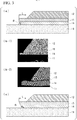
FIG. 3 shows views schematically describing specific examples of a cross-sectional shape of an end portion of a circuit pattern formed in the circuit layer of the power module substrate shown inFIG. 1 , and shows images obtained by SEM observation. -
FIG. 4 shows views schematically describing specific examples of the cross-sectional shape of the end portion of the circuit pattern formed in the circuit layer of the power module substrate shown inFIG. 1 . -
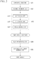
FIG. 5 is a flowchart of a method for manufacturing a power module substrate according to an embodiment of the present invention and a method for manufacturing a power module. -
FIG. 6 is a view schematically describing a method for manufacturing a power module substrate according to an embodiment of the present invention. -
FIG. 7 is a view schematically describing a method for manufacturing a power module according to an embodiment of the present invention. -
FIG. 8 is a view schematically describing a power module in which a power module substrate according to another embodiment of the present invention is used. - Hereinafter, embodiments of the present invention will be described with reference to the attached drawings. In the following description, "brazing filler material" is not limited to materials containing lead.
-
FIG. 1 shows apower module 1 including apower module substrate 10 according to the present embodiment. - The
power module 1 includes thepower module substrate 10 provided with acircuit layer 12 and ametal layer 13, asemiconductor element 3 bonded to one surface (upper surface inFIG. 1 ) of thecircuit layer 12 through abonding layer 2, and aheat sink 30 bonded to the other side (lower side inFIG. 1 ) of thepower module substrate 10 through abonding layer 32. - As shown in
FIG. 1 , thepower module substrate 10 includes aceramic substrate 11, thecircuit layer 12 provided on one surface (upper surface inFIG. 1 ) of theceramic substrate 11, and themetal layer 13 provided on the other surface (lower surface inFIG. 1 ) of theceramic substrate 11. - The
ceramic substrate 11 is constituted with ceramics such as aluminum nitride (AlN), silicon nitride (Si3N4), and alumina (Al2O3) having high insulating properties. In the present embodiment, theceramic substrate 11 is constituted with aluminum nitride (AlN) having excellent heat radiation properties. The thickness of theceramic substrate 11 is set within a range of 0.2 to 1.5 mm. In the present embodiment, the thickness of theceramic substrate 11 is set to be 0.635 mm. - The
circuit layer 12 is formed by bonding aCu foil 22 formed of Cu or a Cu alloy having conductivity to one surface of theceramic substrate 11. - In the present embodiment, as shown in
FIG. 6 , thecircuit layer 12 is formed by laminating a Cu-P-Sn-basedbrazing filler material 24, aTi material 25, and theCu foil 22 formed of oxygen-free copper on one surface of theceramic substrate 11 and performing heating such that theCu foil 22 is bonded to theceramic substrate 11. In the present embodiment, as the Cu-P-Sn-basedbrazing filler material 24, a Cu-P-Sn-Ni brazing filler material is used. - The thickness of the
circuit layer 12 is set within a range equal to or greater than 0.1 mm and equal to or smaller than 1.0 mm. In the present embodiment, the thickness of thecircuit layer 12 is set to be 0.3 mm. - The
metal layer 13 is formed by bonding aCu foil 23 formed of Cu or a Cu alloy to the other surface of theceramic substrate 11 through the Cu-P-Sn-basedbrazing filler material 24. In the present embodiment, as shown inFIG. 6 , themetal layer 13 is formed by laminating the Cu-P-Sn-basedbrazing filler material 24, theTi material 25, and theCu foil 23 formed of oxygen-free copper on the other surface of theceramic substrate 11 and performing a heat treatment such that theCu foil 23 is bonded to theceramic substrate 11. In the present embodiment, as the Cu-P-Sn-basedbrazing filler material 24, a Cu-P-Sn-Ni brazing filler material is used. - The thickness of the
metal layer 13 is set within a range equal to or greater than 0.1 mm and equal to or smaller than 1.0 mm. In the present embodiment, the thickness of themetal layer 13 is set to be 0.3 mm. -
FIG. 2 is a view schematically describing a bonded interface between theceramic substrate 11 and the circuit layer 12 (metal layer 13). As shown inFIG. 2 , in the bonded interface between theceramic substrate 11 and the circuit layer 12 (metal layer 13), a structure is established in which a Cu-Sn layer 14 positioned on theceramic substrate 11 side and a Ti-containinglayer 15 containing Ti are laminated. In the present embodiment, the Ti-containinglayer 15 has a structure in which a firstintermetallic compound layer 16 which contains Ti and P, aTi layer 18, and a secondintermetallic compound layer 17 which contains Cu and Ti are laminated. In the Cu-Sn layer 14, Sn forms a solid solution in Cu. The firstintermetallic compound layer 16 is mainly constituted with Ti and P, theTi layer 18 is mainly constituted with Ti, and the secondintermetallic compound layer 17 is mainly constituted with Cu and Ti. However, these layers may also contain other elements. - The
semiconductor element 3 is constituted with a semiconductor material such as Si. Thesemiconductor element 3 and thecircuit layer 12 are bonded to each other through abonding layer 2. - The
bonding layer 2 is formed of a solder material based on Sn-Ag, Sn-In, or Sn-Ag-Cu, for example. - The
heat sink 30 dissipates the heat from the aforementionedpower module substrate 10. Theheat sink 30 is constituted with Cu or a Cu alloy. In the present embodiment, theheat sink 30 is constituted with phosphorus deoxidized copper. Theheat sink 30 is provided withpassages 31 for a cooling fluid to flow through the passages. In the present embodiment, theheat sink 30 and themetal layer 13 are bonded to each other through thebonding layer 32 formed of a solder material. - In the
circuit layer 12 of thepower module substrate 10 as the present embodiment, a circuit pattern is formed by performing an etching treatment. - In the cross-sectional shape of an end portion of the circuit pattern of the
circuit layer 12, an angle θ formed between a surface of theceramic substrate 11 and an end face of the Cu-Sn layer 14 is set in a range equal to or greater than 80° and equal to or smaller than 100°. Furthermore, a maximum protrusion length L of the Cu-Sn layer 14 or the Ti-containinglayer 15 from an end face of the circuit layer 12 (maximum length of the Cu-Sn layer 14 and the Ti-containinglayer 15 protruding from an end face of the circuit layer 12) is set in a range equal to or greater than 2 µm and equal to or smaller than 15 µm. - The end portion of the circuit pattern is one end portion of wiring included in the circuit pattern. The cross-sectional shape of the end portion of the circuit pattern is the shape of the end portion of the circuit pattern in a cross section which is perpendicular to the surface of the
ceramic substrate 11 and is parallel to the direction along which the wiring in the end portion of the circuit pattern extends. For determining the angle θ, a straight line, which connects the bonding end of theceramic substrate 11 and the Cu-Sn layer 14 in the cross section to a midpoint between the highest point and the lowest point of surface asperities of theceramic substrate 11 that are within a range of 20 µm from the bonding end in a horizontal direction, is defined as the surface of theceramic substrate 11. The maximum protrusion length L is a maximum length between the end of the end face of thecircuit layer 12 on the Ti-containinglayer 15 side in the cross section and end faces of the Cu-Sn layer 14 and the Ti-containinglayer 15 protruding from the end face of thecircuit layer 12, in a direction parallel to the surface of theceramic substrate 11. In order to obtain the effects, which will be described later, obtained by setting the angle θ and the maximum protrusion length L within the range described above, the angle θ and the maximum protrusion length L preferably fall into the aforementioned range in one end portion of at least one wiring included in the circuit pattern, more preferably fall into the aforementioned range in both end portions of at least one wiring included in the circuit pattern, and even more preferably fall into the aforementioned range in both end portions of all wiring of the circuit pattern. - Specific examples of the cross-sectional shape of the end portion of the circuit pattern of the
circuit layer 12 will be described with reference toFIG. 3 andFIG. 4 . - In
FIG. 3(a) , the angle θ formed between the surface of theceramic substrate 11 and the end face of the Cu-Sn layer 14 is approximately 90° in the end portion of the circuit pattern (88° ≤ θ ≤ 92°), and the maximum protrusion length L of the Cu-Sn layer 14 or the Ti-containinglayer 15 from the end face of thecircuit layer 12 is equal to or smaller than 15 µm. Note thatFIG. 3 (b-1) is an image obtained by SEM observation, andFIG. 3 (b-2) is a view obtained by magnifying the vicinity of the end portion of the circuit pattern inFIG. 3 (b-1). As is evident fromFIG. 3 (b-2), the Ti-containinglayer 15 is also observed in the portion protruding from the end face of thecircuit layer 12. - In
FIG. 3(c) , the angle θ formed between the surface of theceramic substrate 11 and the end face of the Cu-Sn layer 14 is within a range greater than 90° and equal to or smaller than 100° in the end portion of the circuit pattern, and the maximum protrusion length L of the Cu-Sn layer 14 or the Ti-containinglayer 15 from the end face of thecircuit layer 12 is equal to or smaller than 15 µm. Furthermore, the end face of the Ti-containinglayer 15 is positioned on an extended plane of the end face of the Cu-Sn layer 14. - In
FIG. 4(a) , the angle θ formed between the surface of theceramic substrate 11 and the end face of the Cu-Sn layer 14 is within a range equal to or greater than 90° and equal to or smaller than 100° in the end portion of the circuit pattern, and the maximum protrusion length L of the Cu-Sn layer 14 or the Ti-containinglayer 15 from the end face of thecircuit layer 12 is equal to or smaller than 15 µm. Furthermore, the end face of the Ti-containinglayer 15 protrudes further toward the outside (direction separating from the end face of the circuit layer 12) compared to the end face of the Cu-Sn layer 14. - In
FIG. 4(b) , the angle θ formed between the surface of theceramic substrate 11 and the end face of the Cu-Sn layer 14 is within a range greater than 80° and less than 90° in the end portion of the circuit pattern, and the maximum protrusion length L of the Cu-Sn layer 14 or the Ti-containinglayer 15 from the end face of thecircuit layer 12 is equal to or smaller than 15 µm. Furthermore, the end face of the Ti-containinglayer 15 protrudes further toward the outside compared to the end face of the Cu-Sn layer 14. - In
FIG. 4(c) , the angle θ formed between the surface of theceramic substrate 11 and the end face of the Cu-Sn layer 14 is within a range greater than 90° and equal to or smaller than 100° in the end portion of the circuit pattern, and the maximum protrusion length L of the Cu-Sn layer 14 or the Ti-containinglayer 15 from the end face of thecircuit layer 12 is equal to or smaller than 15 µm. Furthermore, the end face of the Cu-Sn layer 14 protrudes further toward the outside compared to the end face of the Ti-containinglayer 15. - In the shapes shown in
FIG. 3(a) and FIG. 3(c) , the end face of the Ti-containinglayer 15 is positioned on an extended plane of the end face of the Cu-Sn layer 14. It is difficult for charges to be concentrated on the interface between the Ti-containinglayer 15 and the Cu-Sn layer 14, and the deterioration of partial discharge characteristics and voltage endurance characteristics can be sufficiently inhibited. - Note that in the shapes shown in
FIG. 4(a), FIG. 4(b), and FIG. 4(c) , in a case where the angle θ formed between the surface of theceramic substrate 11 and the end face of the Cu-Sn layer 14 is set within a range equal to or greater than 80° and equal to or smaller than 100°, and the maximum protrusion length L of the Cu-Sn layer 14 or the Ti-containinglayer 15 from the end face of thecircuit layer 12 is set within a range equal to or greater than 2 µm and equal to or smaller than 15 µm, it is possible to obtain an effect of inhibiting the deterioration of partial discharge characteristics and voltage endurance characteristics. - The angle θ is preferably equal to or greater than 85° and equal to or smaller than 95° and more preferably equal to or greater than 88° and equal to or smaller than 92°, but is not limited to these. Furthermore, the maximum protrusion length L is preferably equal to or smaller than 10 µm and more preferably equal to or smaller than 5 µm, but is not limited to these.
- Next, a method for manufacturing the
power module substrate 10 as the present embodiment will be described with reference toFIG. 5 andFIG. 6 . - First, as shown in
FIG. 6 , the Cu-P-Sn-basedbrazing filler material 24, theTi material 25, and theCu foil 22 which becomes thecircuit layer 12 are laminated in this order on one surface (upper surface inFIG. 6 ) of theceramic substrate 11, and the Cu-P-Sn-basedbrazing filler material 24, theTi material 25, and theCu foil 23 which becomes themetal layer 13 are laminated in this order on the other surface (lower surface inFIG. 6 ) of the ceramic substrate 11 (FIG. 6(a) ). That is, between theceramic substrate 11 and theCu foil 22 and between theceramic substrate 11 and theCu foil 23, the Cu-P-Sn-basedbrazing filler material 24 is disposed on theceramic substrate 11 side, and theTi material 25 is disposed on theCu foil 22 side and theCu foil 23 side. The bonding surface between theTi material 25 and theCu foil - In the present embodiment, the composition of the Cu-P-Sn-based
brazing filler material 24 is Cu-6.3 mass% P-9.3 mass% Sn-7 mass% Ni. The solidus temperature (melting start temperature) of the Cu-P-Sn-basedbrazing filler material 24 is 600°C. Furthermore, in the present embodiment, as the Cu-P-Sn-basedbrazing filler material 24, a foil material is used, and the thickness thereof is within a range equal to or greater than 5 µm and equal to or smaller than 150 µm. - The thickness of the
Ti material 25 is within a range equal to or greater than 0.4 µm and equal to or smaller than 5 µm. In a case where the thickness of theTi material 25 is equal to or greater than 0.4 µm and less than 1 µm, it is preferable to deposit theTi material 25 by vapor deposition or sputtering. In a case where the thickness of theTi material 25 is equal to or greater than 1 µm and equal to or smaller than 5 µm, it is preferable to use a foil material. The lower limit of the thickness of theTi material 25 is preferably equal to or greater than 0.4 µm, and more preferably equal to or greater than 0.5 µm. The upper limit of the thickness of theTi material 25 is preferably equal to or smaller than 1.5 µm, and more preferably equal to or smaller than 0.7 µm. In the present embodiment, as theTi material 25, a Ti foil having a thickness of 1 µm and a purity of 99.8 mass% is used. - Then, the
Cu foil 22, theTi material 25, the Cu-P-Sn-basedbrazing filler material 24, theceramic substrate 11, the Cu-P-Sn-basedbrazing filler material 24, theTi material 25, and theCu foil 23 are put into a vacuum heating furnace in a state where pressure (equal to or higher than 1 kgf/cm2 and equal to or lower than 35 kgf/cm2 (equal to or higher than 0.10 MPa and equal to or lower than 3.43 MPa)) is applied thereto in the lamination direction, and heated (FIG. 6(b) ). In the present embodiment, the internal pressure of the vacuum heating furnace is set within a range equal to or higher than 10-6 Pa and equal to or lower than 10-3 Pa, the heating temperature is set within a range equal to or higher than 560°C and equal to or lower than 650°C, and the heating time is set within a range equal to or longer than 30 minutes and equal to or shorter than 360 minutes. - In the heat treatment step S02, the
Ti material 25 and the Cu foils 22 and 23 are bonded to each other by diffusion in solids, and the Cu-P-Sn-basedbrazing filler material 24 is melted and forms a liquid phase. By the solidification of the liquid phase, through the Cu-P-Sn-basedbrazing filler material 24, theceramic substrate 11 and theTi material 25 are bonded to each other. At this time, in the bonded interface between thecircuit layer 12 and theceramic substrate 11 and between themetal layer 13 and theceramic substrate 11, the Cu-Sn layer 14 and the Ti-containinglayer 15 are formed. - Accordingly, the
circuit layer 12 is formed on one surface of theceramic substrate 11, and themetal layer 13 is formed on the other surface of theceramic substrate 11. - Then, by performing an etching treatment on the
circuit layer 12, a circuit pattern is formed. - In the present embodiment, first, a resist film is deposited on the circuit layer, and the
circuit layer 12 formed of Cu or a Cu alloy is etched (Cu etching step S31). In the Cu etching step S31, it is preferable to use an etching agent containing, for example, ferric chloride, cupric chloride, sulfuric acid, and the like. In the present embodiment, in the Cu etching step S31, a spray etching method is used (FIG. 6(c) ). - After the Cu etching step S31, the Ti-containing
layer 15 is etched (Ti etching step S32). In the Ti etching step S32, it is preferable to use an etching agent obtained by, for example, adding organic acid ammonium to aqueous hydrogen peroxide. As the etching agent, for example, SOLFINE (SE-TW-10) manufactured by SHOWA DENKO K.K. can be used. - The etching may be performed under the conditions of a temperature of 70°C to 80°C and an etching time of 5 minutes to 20 minutes. Note that in the present embodiment, an immersion etching method is used in the Ti etching step S32 (
FIG. 6(d) ). - After the Ti etching step S32, the Cu-
Sn layer 14 is etched (Cu-Sn etching step S33). In the Cu-Sn etching step S33, for example, an aqueous ammonium peroxydisulfate solution can be used. The etching may be performed under the conditions of a liquid temperature of 25°C (room temperature) and an etching time of 10 minutes to 20 minutes. Note that in the present embodiment, an immersion etching method is used in the Cu-Sn etching step S33 (FIG. 6(e) ). - By the circuit pattern forming step S03, a circuit pattern is formed on the
circuit layer 12. Furthermore in the cross-sectional shape of the end portion of the circuit pattern, the angle θ formed between the surface of theceramic substrate 11 and the end face of the Cu-Sn layer 14 is set in a range equal to or greater than 80° and equal to or smaller than 100°, and the maximum protrusion length L of the Cu-Sn layer 14 or the Ti-containinglayer 15 from the end face of thecircuit layer 12 is set in a range equal to or greater than 2 µm and equal to or smaller than 15 µm. Note that by etching, it is difficult to make the maximum protrusion length L become less than 2 µm. - Through the steps described above, the
power module substrate 10 as the present embodiment is manufactured. - Then, as shown in
FIG. 7 , through a solder material as thebonding layer 32, theheat sink 30 is bonded to the lower surface of themetal layer 13 of the power module substrate 10 (FIG. 7(a) ). - Thereafter, as shown in
FIG. 7 , through a solder material, thesemiconductor element 3 is bonded to the upper surface of thecircuit layer 12 of the power module substrate 10 (FIGS. 7(b) and 7(c) ). - In this way, the
power module 1 shown inFIG. 1 is manufactured. - According to the
power module substrate 10 as the present embodiment that is manufactured as described above, a circuit pattern is formed in thecircuit layer 12 formed of Cu or a Cu alloy, and in the cross-sectional shape of the end portion of the circuit pattern of thecircuit layer 12, the angle θ formed between the surface of theceramic substrate 11 and the end face of the Cu-Sn layer 14 is set in a range equal to or greater than 80° and equal to or smaller than 100°. Therefore, in the end portion of the circuit pattern, a site having an acute-angled shape is not formed, and hence charge concentration can be inhibited. As a result, it is possible to inhibit the deterioration of partial discharge characteristics and voltage endurance characteristics. - Furthermore, the maximum protrusion length L of the Cu-
Sn layer 14 or the Ti-containinglayer 15 from the end face of thecircuit layer 12 is set in a range equal to or greater than 2 µm and equal to or smaller than 15 µm. Therefore, it is possible to inhibit charges from being concentrated on the tip of the protruding portion and to inhibit the deterioration of partial discharge characteristics and voltage endurance characteristics. - In addition, in the present embodiment, as shown in
FIG. 3(c) , in a case where the end face of the Ti-containinglayer 15 is positioned on an extended plane of the end face of the Cu-Sn layer 14 in the cross-sectional shape of the end portion of the circuit pattern of thecircuit layer 12, the Cu-Sn layer 14 and the Ti-containinglayer 15 are smoothly connected to each other. Accordingly, it is possible to inhibit charges from being concentrated on the interface between the Cu-Sn layer 14 and the Ti-containinglayer 15 and to further inhibit the deterioration of partial discharge characteristics and voltage endurance characteristics. - Hitherto, an embodiment of the present invention has been described. However, the present invention is not limited thereto and can be appropriately modified within a scope that does not depart from the technical idea of the present invention.
- In the present embodiment, a case where a metal layer formed of Cu or a Cu alloy is formed on the other surface of a ceramic substrate has been described, but the present invention is not limited thereto. The metal layer may not be formed, or a metal layer formed of Al or an Al alloy may be formed.
- Specifically, as shown in
FIG. 8 , apower module substrate 110 may be adopted in which thecircuit layer 12 formed of Cu or a Cu alloy is formed on one surface of theceramic substrate 11, and a metal layer 113 formed of Al or an Al alloy is formed on the other surface of theceramic substrate 11. By bonding aheat sink 130 includingpassages 131 and thesemiconductor element 3 to thepower module substrate 110, apower module 101 shown inFIG. 8 is constituted. - In the
power module substrate 110, it is possible to simultaneously perform a step of forming thecircuit layer 12 by bonding a copper foil to one surface of theceramic substrate 11 by using a Cu-P-Sn-based brazing filler material and a Ti material and a step of bonding an Al foil formed of Al or an Al alloy to the other surface of theceramic substrate 11 by using a brazing filler material. Furthermore, in a case where theheat sink 130 made of Al is used, a step of brazing the metal layer 113 and theheat sink 130 can also be simultaneously performed. - The material or the structure of the heat sink is not limited to the present embodiment, and a design change may be appropriately carried out. Alternatively, the power module substrate may not have a heat sink.
- Furthermore, in the present embodiment, a constitution has been described in which the power module substrate and the heat sink are bonded to each other by using a solder material. However, a constitution may be adopted in which the power module substrate and the heat sink are fastened to each other by a screw and the like through grease provided therebetween.
- In addition, the etching agent used in each of the Cu etching step S31, the Ti etching step S32, and the Cu-Sn etching step S33 is not limited to those exemplified in the present embodiment. It is preferable to select and use etching agents suitable for each of these steps, according to the material and the structure of the circuit layer, the material and the structure of the Ti-containing layer, the material and the structure of the Cu-Sn layer, and the like.
- In the above embodiments, a case where a foil material of a Cu-P-Sn-based brazing filler material is used was described for example. However, the present invention is not limited thereto, and powder or paste can also be used.
- Furthermore, in the above embodiments, a case where a Cu-P-Sn-Ni brazing filler material or a Cu-P-Sn brazing filler material is used as the Cu-P-Sn-based brazing filler material was described. However, other Cu-P-Sn-based brazing filler materials may also be used.
- Herein, the content of P in the Cu-P-Sn-based brazing filler material is preferably equal to or greater than 3 mass% and equal to or smaller than 10 mass%.
- P is an element having an operation and effect of reducing the melting start temperature of the brazing filler material. In a case where P is oxidized, P oxide occurs. P is an element having an operation and effect of coating the surface of the brazing filler material with the P oxide so as to prevent the oxidation of the brazing filler material, and coating the surface of the molten brazing filler material with the P oxide having excellent fluidity so as to improve the wettability of the brazing filler material.
- In a case where the content of P is less than 3 mass%, the effect of reducing the melting start temperature of the brazing filler material may not be sufficiently obtained. Accordingly, the melting start temperature of the brazing filler material may be increased or the fluidity of the brazing filler material may become insufficient. As a result, the bonding properties between the ceramic substrate and the circuit layer may be reduced. Furthermore, in a case where the content of P is greater than 10 mass%, a large amount of brittle intermetallic compound may be formed. As a result, the bonding properties and the bonding reliability between the ceramic substrate and the circuit layer may be reduced.
- For these reasons, the content of P in the Cu-P-Sn-based brazing filler material is preferably within a range equal to or greater than 3 mass% and equal to or smaller than 10 mass%.
- The content of Sn in the Cu-P-Sn-based brazing filler material is preferably equal to or greater than 0.5 mass% and equal to or smaller than 25 mass%.
- Sn is an element having an operation and effect of reducing the melting start temperature of the brazing filler material. In a case where the content of Sn is equal to or greater than 0.5 mass%, the melting start temperature of the brazing filler material can be reliably reduced.
- In a case where the content of Sn is equal to or smaller than 25 mass%, it is possible to inhibit the brazing filler material from becoming brittle at a low temperature and to improve the bonding reliability between the ceramic substrate and the circuit layer.
- For these reasons, the content of Sn in the Cu-P-Sn-based brazing filler material is preferably within a range equal to or greater than 0.5 mass% and equal to or smaller than 25 mass%.
- The Cu-P-Sn-based brazing filler material may contain one kind of element or two or more kinds of elements among Ni, Cr, Fe, and Mn in an amount equal to or greater than 2 mass% and equal to or smaller than 20 mass%.
- Ni, Cr, Fe, and Mn are elements having an operation and effect of inhibiting the formation of an intermetallic compound containing P in the interface between the ceramic substrate and the brazing filler material.
- In a case where the content of one kind of element or two or more kinds of elements among Ni, Cr, Fe, and Mn is equal to or greater than 2 mass%, the formation of an intermetallic compound containing P in the bonded interface between the ceramic substrate and the brazing filler material can be inhibited, and the bonding reliability between the ceramic substrate and the circuit layer can be improved. Furthermore, in a case where the content of one kind of element or two or more kinds of elements among Ni, Cr, Fe, and Mn is equal to or smaller than 20 mass%, it is possible to inhibit the increase of the melting start temperature of the brazing filler material, to inhibit the decrease of the fluidity of the brazing filler material, and to improve the bonding properties between the ceramic substrate and the circuit layer.
- For these reasons, in a case where the Cu-P-Sn-based brazing filler material contains one kind of element or two or more kinds of elements among Ni, Cr, Fe, and Mn, the content of the element is preferably within a range equal to or greater than 2 mass% and equal to or smaller than 20 mass%.
- Hereinafter, the results of experiments performed to check the effects of the present invention will be described.
- According to the procedure described in the embodiment described above, each of the Cu foils (46 mm × 56 mm × 0.3 mm (thickness)) shown in Table 1 and Table 2 was bonded to one surface and the other surface of each of the ceramic substrates (50 mm × 60 mm × 0.635 mm (thickness) (AlN), 50 mm × 60 mm × 0.32 mm (thickness) (Si3N4)) shown in Table 1 and Table 2, thereby forming a circuit layer and a metal layer. As the Cu foil, oxygen-free copper ("OFC" in Tables 1 and 2) or tough pitch copper ("Tough pitch" in Tables 1 and 2) was used. A Cu-P-Sn-based brazing filler material having a thickness of 25 µm was used.
- Then, the etching treatment described in the embodiment described above was performed on the circuit layer, thereby forming a circuit pattern having an interwiring distance of 500 µm. Specifically, in the Cu etching step S31, by using iron chloride as an etching agent, spray etching was performed for 5 to 15 minutes at a liquid temperature of 50°C to 70°C. In the Ti etching step S32, by using SOLFINE (SE-TW-10) manufactured by SHOWA DENKO K.K. as an etching agent, immersion etching was performed for 5 to 20 minutes by setting the liquid temperature of the etching agent to be 70°C to 80°C. In the Cu-Sn etching step S33, by using an aqueous ammonium peroxydisulfate solution having a concentration of 1 mol/dm3 as an etching agent, immersion etching was performed for 10 to 20 minutes by setting the liquid temperature of the etching agent to be 25°C.
- Thereafter, a cross section of an end portion of the circuit pattern in the obtained power module substrate was observed, and the angle θ formed between the surface of the ceramic substrate and the end face of the Cu-Sn layer and the maximum protrusion length L of the Cu-Sn layer or the Ti-containing layer from the end face of the circuit layer were measured. Note that the "Form" described in Table 1 and Table 2 shows to which form the example belongs among the drawings.
- During the observation of the cross section, by using a cross section polisher (SM-09010 manufactured by JEOL Ltd.), ion etching was performed on a cross section of the circuit layer (cross section which is perpendicular to the surface of the ceramic substrate and is parallel to the direction along which wiring extends in the end portion of the circuit pattern) under the conditions of an ion accelerating voltage: 5 kV, a processing time: 14 hours, and a protrusion amount from a masking shield: 100 µm, and then the end portion of the circuit pattern was observed using a scanning electron microscope (SEM).
- For evaluating the voltage endurance characteristics of the obtained power module substrates, a cycle was repeated in which each of the power module substrates was immersed in insulating oil (FLUORINERT FC-770 manufactured by 3M), voltage was increased to 0.5 kV for 5 seconds, and then the power module substrate was kept as it was for 30 seconds. A voltage at a point in time when the amount of discharged charges exceeded 10 pC while the power module substrate was being kept as it was taken as a partial discharge start voltage, and partial discharge characteristics were evaluated. The evaluation results are shown in Table 1 and Table 2.
[Table 1] Ceramic substrate Cu foil Cross-sectional shape of end portion of circuit pattern Evaluation Angle θ (°) Maximum protrusion length L (µm) Form Partial discharge start voltage (kV) Example 1 AlN OFC 88 2.3 FIG. 3(a) 11.0 Example 2 AlN OFC 91 14.7 FIG. 3(a) 8.5 Example 3 AlN OFC 85 2.3 FIG. 3(c) 11.0 Example 4 AlN OFC 95 14.7 FIG. 3(c) 8.5 Example 5 AlN OFC 81 9.8 FIG. 3(c) 9.0 Example 6 AlN OFC 98 8.6 FIG. 3(c) 10.0 Example 7 AlN OFC 93 2.2 FIG. 4(d) 10.5 Example 8 AlN OFC 87 14.8 FIG. 4(d) 8.5 Example 9 AlN OFC 82 9.8 FIG. 4(d) 9.0 Example 10 AlN OFC 99 8.6 FIG. 4(d) 9.5 Example 11 AlN OFC 94 8.8 FIG. 4(e) 9.5 Example 12 AlN OFC 86 9.2 FIG. 4(f) 9.0 Example 13 AlN TOUGH PITCH 87 5.3 FIG. 3(c) 9.5 Comparative Example 1 AlN OFC 87 30.0 FIG. 3(c) 7.0 Comparative Example 2 AlN OFC 65 8.6 FIG. 3(c) 7.0 Comparative Example 3 AlN OFC 112 9.4 FIG. 3(c) 7.5 [Table 2] Ceramic substrate Cu foil Cross-sectional shape of end portion of circuit pattern Evaluation Angle θ (°) Maximum protrusion length L (µm) Form Partial discharge start voltage (kV) Example 14 Si3N4 OFC 89 2.2 FIG. 3(a) 9.5 Example 15 Si3N4 OFC 91 14.5 FIG. 3(a) 7.0 Example 16 Si3N4 OFC 87 2.3 FIG. 3(c) 9.5 Example 17 Si3N4 OFC 94 14.8 FIG. 3(c) 7.0 Example 18 Si3N4 OFC 80 9.5 FIG. 3(c) 7.0 Example 19 Si3N4 OFC 99 7.9 FIG. 3(c) 8.5 Example 20 Si3N4 OFC 92 2.3 FIG. 4(d) 9.0 Example 21 Si3N4 OFC 85 14.6 FIG 4(d) 7.0 Example 22 Si3N4 OFC 82 8.6 FIG. 4(d) 7.5 Example 23 Si3N4 OFC 99 8.8 FIG. 4(d) 7.5 Example 24 Si3N4 OFC 93 8.6 FIG. 4(e) 8.0 Example 25 Si3N4 OFC 86 8.7 FIG. 4(f) 7.5 Example 26 Si3N4 TOUGH PITCH 88 4.9 FIG. 3(c) 8.0 Comparative Example 4 Si3N4 OFC 87 30.0 FIG. 3(c) 5.0 Comparative Example 5 Si3N4 OFC 67 8.7 FIG. 3(c) 5.5 Comparative Example 6 Si3N4 OFC 115 8.2 FIG. 3(c) 5.5 - Regarding the results shown in Table 1 obtained by using AlN as a ceramic substrate, it was understood that in the examples of the present invention, in which the angle θ formed between the surface of the ceramic substrate and the end face of the Cu-Sn layer is set in a range equal to or greater than 80° and equal to or smaller than 100° and the maximum protrusion length L of the Cu-Sn layer or the Ti-containing layer from the end face of the circuit layer is set in a range equal to or greater than 2 µm and equal to or smaller than 15 µm, a power module substrate is obtained which has a high partial discharge start voltage and is excellent in partial discharge characteristics and voltage endurance characteristics.
- The results shown in Table 2 obtained using Si3N4 as a ceramic substrate were the same as the results obtained using AlN.
- According to the present invention, it is possible to inhibit the occurrence of partial discharge in a circuit layer formed on one surface of the ceramic substrate and to inhibit the occurrence of short-circuit even though a fine circuit pattern is formed. Therefore, the present invention is suitable for power semiconductor elements for high power control that are used for controlling wind power generation and electric vehicles such as electric cars.
-
- 10, 110
- power module substrate
- 11
- ceramic substrate
- 12
- circuit layer
- 14
- Cu-Sn layer
- 15
- Ti-containing layer
Claims (2)
- A power module substrate comprising:a ceramic substrate; anda circuit layer which is formed on one surface of the ceramic substrate and has a circuit pattern,wherein the circuit layer is made of Cu or a Cu alloy,in an interface between the circuit layer and the ceramic substrate, a Cu-Sn layer in which Sn forms a solid solution in Cu and a Ti-containing layer containing Ti are laminated in this order from the ceramic substrate side, andin a cross-sectional shape of an end portion of the circuit pattern of the circuit layer, an angle θ formed between a surface of the ceramic substrate and an end face of the Cu-Sn layer is set in a range equal to or greater than 80° and equal to or smaller than 100°, and a maximum protrusion length L of the Cu-Sn layer or the Ti-containing layer from an end face of the circuit layer is set in a range equal to or greater than 2 µm and equal to or smaller than 15 µm.
- The power module substrate according to claim 1,
wherein in the cross-sectional shape of the end portion of the circuit pattern of the circuit layer, an end face of the Ti-containing layer is positioned on an extended plane of the end face of the Cu-Sn layer.
Applications Claiming Priority (2)
| Application Number | Priority Date | Filing Date | Title |
|---|---|---|---|
| JP2016100615 | 2016-05-19 | ||
| PCT/JP2017/018518 WO2017200004A1 (en) | 2016-05-19 | 2017-05-17 | Substrate for power modules |
Publications (3)
| Publication Number | Publication Date |
|---|---|
| EP3460838A1 true EP3460838A1 (en) | 2019-03-27 |
| EP3460838A4 EP3460838A4 (en) | 2019-12-25 |
| EP3460838B1 EP3460838B1 (en) | 2021-02-24 |
Family
ID=60325210
Family Applications (1)
| Application Number | Title | Priority Date | Filing Date |
|---|---|---|---|
| EP17799428.2A Active EP3460838B1 (en) | 2016-05-19 | 2017-05-17 | Substrate for power modules |
Country Status (6)
| Country | Link |
|---|---|
| US (1) | US10453783B2 (en) |
| EP (1) | EP3460838B1 (en) |
| JP (1) | JP6687109B2 (en) |
| CN (1) | CN109155291B (en) |
| TW (1) | TWI713746B (en) |
| WO (1) | WO2017200004A1 (en) |
Cited By (3)
| Publication number | Priority date | Publication date | Assignee | Title |
|---|---|---|---|---|
| EP4191661A4 (en) * | 2020-07-27 | 2024-08-21 | Kabushiki Kaisha Toshiba | ASSEMBLED BODY, CIRCUIT BOARD, SEMICONDUCTOR DEVICE AND METHOD FOR MANUFACTURING ASSEMBLED BODY |
| EP4190764A4 (en) * | 2020-07-27 | 2024-08-21 | Kabushiki Kaisha Toshiba | JUNCTION BODY, CIRCUIT SUBSTRATE, SEMICONDUCTOR DEVICE, AND METHOD FOR MANUFACTURING JUNCTION BODY |
| EP4203014A4 (en) * | 2020-11-06 | 2024-10-02 | Zhenghai Group Co., Ltd. | HEAT DISSIPATION STRUCTURE OF A COOLING PLATE FOR A POWER SEMICONDUCTOR MODULE |
Families Citing this family (7)
| Publication number | Priority date | Publication date | Assignee | Title |
|---|---|---|---|---|
| JP7289910B2 (en) * | 2019-03-14 | 2023-06-12 | 日本碍子株式会社 | BONDED SUBSTRATE AND BONDED SUBSTRATE MANUFACTURING METHOD |
| WO2020183701A1 (en) * | 2019-03-14 | 2020-09-17 | 日本碍子株式会社 | Bonded substrate |
| KR102122210B1 (en) * | 2019-10-18 | 2020-06-12 | 제엠제코(주) | Heat sink board, manufacturing method thereof, and semiconductor package including the same |
| JP7301732B2 (en) * | 2019-12-24 | 2023-07-03 | 株式会社東芝 | Ceramic circuit board with screw pad member and semiconductor device using the same |
| CN120097746A (en) * | 2020-10-07 | 2025-06-06 | 株式会社东芝 | Joint body, ceramic circuit substrate and semiconductor device |
| EP4032870A1 (en) * | 2021-01-22 | 2022-07-27 | Heraeus Deutschland GmbH & Co. KG | Structured metal / ceramic substrate and method for structuring metal-ceramic substrates |
| JPWO2023120185A1 (en) * | 2021-12-24 | 2023-06-29 |
Family Cites Families (13)
| Publication number | Priority date | Publication date | Assignee | Title |
|---|---|---|---|---|
| JP3845925B2 (en) * | 1996-02-05 | 2006-11-15 | 住友電気工業株式会社 | Semiconductor device member using aluminum nitride substrate and method for manufacturing the same |
| JP3449458B2 (en) | 1997-05-26 | 2003-09-22 | 電気化学工業株式会社 | Circuit board |
| JP4088394B2 (en) * | 1999-09-29 | 2008-05-21 | 株式会社日立製作所 | Insulated circuit board and semiconductor device using the same |
| JP2004172182A (en) * | 2002-11-18 | 2004-06-17 | Denki Kagaku Kogyo Kk | Circuit board and method of manufacturing the same |
| JP4375730B2 (en) | 2004-04-23 | 2009-12-02 | 本田技研工業株式会社 | Brazing material for joining copper and ceramics or carbon-based copper composite material and joining method therefor |
| DE102009033029A1 (en) * | 2009-07-02 | 2011-01-05 | Electrovac Ag | Electronic device |
| TWI455286B (en) * | 2010-10-11 | 2014-10-01 | 台達電子工業股份有限公司 | Power module and method for manufacturing power module |
| KR101659194B1 (en) * | 2011-12-20 | 2016-09-22 | 가부시끼가이샤 도시바 | Ceramic copper circuit board and semiconductor device employing same |
| CN104718615B (en) * | 2012-10-04 | 2018-01-02 | 株式会社东芝 | Semiconductor circuit board and its manufacture method and use its semiconductor device |
| WO2014175459A1 (en) * | 2013-04-26 | 2014-10-30 | 京セラ株式会社 | Composite laminate and electronic device |
| KR102131484B1 (en) * | 2013-08-26 | 2020-07-07 | 미쓰비시 마테리알 가부시키가이샤 | Assembly and power-module substrate |
| JP6079505B2 (en) | 2013-08-26 | 2017-02-15 | 三菱マテリアル株式会社 | Bonded body and power module substrate |
| EP3196927B1 (en) * | 2014-07-02 | 2019-04-17 | Mitsubishi Materials Corporation | Joined body manufacturing method |
-
2017
- 2017-05-17 WO PCT/JP2017/018518 patent/WO2017200004A1/en not_active Ceased
- 2017-05-17 US US16/301,093 patent/US10453783B2/en active Active
- 2017-05-17 JP JP2018518331A patent/JP6687109B2/en active Active
- 2017-05-17 CN CN201780030391.3A patent/CN109155291B/en active Active
- 2017-05-17 EP EP17799428.2A patent/EP3460838B1/en active Active
- 2017-05-18 TW TW106116472A patent/TWI713746B/en not_active IP Right Cessation
Cited By (5)
| Publication number | Priority date | Publication date | Assignee | Title |
|---|---|---|---|---|
| EP4191661A4 (en) * | 2020-07-27 | 2024-08-21 | Kabushiki Kaisha Toshiba | ASSEMBLED BODY, CIRCUIT BOARD, SEMICONDUCTOR DEVICE AND METHOD FOR MANUFACTURING ASSEMBLED BODY |
| EP4190764A4 (en) * | 2020-07-27 | 2024-08-21 | Kabushiki Kaisha Toshiba | JUNCTION BODY, CIRCUIT SUBSTRATE, SEMICONDUCTOR DEVICE, AND METHOD FOR MANUFACTURING JUNCTION BODY |
| US12347744B2 (en) | 2020-07-27 | 2025-07-01 | Kabushiki Kaisha Toshiba | Bonded body including titanium alloy at bonding boundary |
| US12431406B2 (en) | 2020-07-27 | 2025-09-30 | Kabushiki Kaisha Toshiba | Bonded body, circuit board, semiconductor device, and method for manufacturing bonded body |
| EP4203014A4 (en) * | 2020-11-06 | 2024-10-02 | Zhenghai Group Co., Ltd. | HEAT DISSIPATION STRUCTURE OF A COOLING PLATE FOR A POWER SEMICONDUCTOR MODULE |
Also Published As
| Publication number | Publication date |
|---|---|
| JP6687109B2 (en) | 2020-04-22 |
| US10453783B2 (en) | 2019-10-22 |
| EP3460838B1 (en) | 2021-02-24 |
| EP3460838A4 (en) | 2019-12-25 |
| CN109155291B (en) | 2022-05-03 |
| JPWO2017200004A1 (en) | 2019-04-04 |
| TWI713746B (en) | 2020-12-21 |
| US20190189548A1 (en) | 2019-06-20 |
| WO2017200004A1 (en) | 2017-11-23 |
| TW201816952A (en) | 2018-05-01 |
| CN109155291A (en) | 2019-01-04 |
Similar Documents
| Publication | Publication Date | Title |
|---|---|---|
| EP3460838B1 (en) | Substrate for power modules | |
| EP3632879B1 (en) | Ceramic circuit board and method of production | |
| CN109417056B (en) | Copper-ceramic joined body and insulated circuit board | |
| KR102272865B1 (en) | Joined body, substrate for power module provided with heat sink, heat sink, method for manufacturing joined body, method for manufacturing substrate for power module provided with heat sink, and method for manufacturing heat sink | |
| EP3285292A1 (en) | Bonded body, substrate for power module with heat sink, heat sink, method for producing bonded body, method for producing substrate for power module with heat sink, and method for producing heat sink | |
| EP3196930B1 (en) | Bonded body, power module substrate with heat sink, use of the bonded body as a heat sink, method for manufacturing bonded body | |
| EP2282334A1 (en) | Substrate for power module, power module, and method for producing substrate for power module | |
| EP3269491B1 (en) | Manufacturing method for junction, manufacturing method for substrate for power module with heat sink, and manufacturing method for heat sink | |
| JP2011124585A (en) | Ceramic wiring board and manufacturing method and semiconductor module of the same | |
| EP3279936B1 (en) | Method for manufacturing substrate for power module with heat sink | |
| EP4585581A1 (en) | Copper/ceramic bonded body and insulated circuit board | |
| TWI711141B (en) | Semiconductor device | |
| EP3407380B1 (en) | Bonded body, power module substrate, bonded body manufacturing method, and power module substrate manufacturing method | |
| KR102524698B1 (en) | Assembly, power module substrate, power module, assembly method and manufacturing method of power module substrate | |
| US12199006B2 (en) | Bonded body, power module substrate, power module, method for manufacturing bonded body, and method for manufacturing power module substrate | |
| KR20220110740A (en) | Copper/ceramic bonded body, insulated circuit board, and copper/ceramic bonded body manufacturing method, insulated circuit board manufacturing method | |
| JP2022165046A (en) | Copper/ceramic assembly and insulation circuit board | |
| EP4328208A1 (en) | Copper/ceramic bonded body and insulated circuit board | |
| US20240414841A1 (en) | Copper/ceramic joined body and insulated circuit board | |
| WO2022224958A1 (en) | Copper/ceramic bonded body and insulated circuit board |
Legal Events
| Date | Code | Title | Description |
|---|---|---|---|
| STAA | Information on the status of an ep patent application or granted ep patent |
Free format text: STATUS: THE INTERNATIONAL PUBLICATION HAS BEEN MADE |
|
| PUAI | Public reference made under article 153(3) epc to a published international application that has entered the european phase |
Free format text: ORIGINAL CODE: 0009012 |
|
| STAA | Information on the status of an ep patent application or granted ep patent |
Free format text: STATUS: REQUEST FOR EXAMINATION WAS MADE |
|
| 17P | Request for examination filed |
Effective date: 20181115 |
|
| AK | Designated contracting states |
Kind code of ref document: A1 Designated state(s): AL AT BE BG CH CY CZ DE DK EE ES FI FR GB GR HR HU IE IS IT LI LT LU LV MC MK MT NL NO PL PT RO RS SE SI SK SM TR |
|
| AX | Request for extension of the european patent |
Extension state: BA ME |
|
| RAP1 | Party data changed (applicant data changed or rights of an application transferred) |
Owner name: MITSUBISHI MATERIALS CORPORATION |
|
| DAV | Request for validation of the european patent (deleted) | ||
| DAX | Request for extension of the european patent (deleted) | ||
| A4 | Supplementary search report drawn up and despatched |
Effective date: 20191126 |
|
| RIC1 | Information provided on ipc code assigned before grant |
Ipc: H01L 23/373 20060101ALI20191120BHEP Ipc: H05K 3/38 20060101ALI20191120BHEP Ipc: H01L 23/36 20060101ALI20191120BHEP Ipc: C04B 37/02 20060101ALI20191120BHEP Ipc: H05K 1/03 20060101ALI20191120BHEP Ipc: H01L 23/13 20060101AFI20191120BHEP Ipc: B23K 35/22 20060101ALI20191120BHEP Ipc: H01L 23/12 20060101ALI20191120BHEP |
|
| GRAP | Despatch of communication of intention to grant a patent |
Free format text: ORIGINAL CODE: EPIDOSNIGR1 |
|
| STAA | Information on the status of an ep patent application or granted ep patent |
Free format text: STATUS: GRANT OF PATENT IS INTENDED |
|
| INTG | Intention to grant announced |
Effective date: 20201023 |
|
| GRAS | Grant fee paid |
Free format text: ORIGINAL CODE: EPIDOSNIGR3 |
|
| GRAA | (expected) grant |
Free format text: ORIGINAL CODE: 0009210 |
|
| STAA | Information on the status of an ep patent application or granted ep patent |
Free format text: STATUS: THE PATENT HAS BEEN GRANTED |
|
| AK | Designated contracting states |
Kind code of ref document: B1 Designated state(s): AL AT BE BG CH CY CZ DE DK EE ES FI FR GB GR HR HU IE IS IT LI LT LU LV MC MK MT NL NO PL PT RO RS SE SI SK SM TR |
|
| REG | Reference to a national code |
Ref country code: CH Ref legal event code: EP |
|
| REG | Reference to a national code |
Ref country code: AT Ref legal event code: REF Ref document number: 1365555 Country of ref document: AT Kind code of ref document: T Effective date: 20210315 Ref country code: CH Ref legal event code: NV Representative=s name: VALIPAT S.A. C/O BOVARD SA NEUCHATEL, CH |
|
| REG | Reference to a national code |
Ref country code: IE Ref legal event code: FG4D |
|
| REG | Reference to a national code |
Ref country code: DE Ref legal event code: R096 Ref document number: 602017033411 Country of ref document: DE |
|
| REG | Reference to a national code |
Ref country code: LT Ref legal event code: MG9D |
|
| REG | Reference to a national code |
Ref country code: NL Ref legal event code: MP Effective date: 20210224 |
|
| PG25 | Lapsed in a contracting state [announced via postgrant information from national office to epo] |
Ref country code: GR Free format text: LAPSE BECAUSE OF FAILURE TO SUBMIT A TRANSLATION OF THE DESCRIPTION OR TO PAY THE FEE WITHIN THE PRESCRIBED TIME-LIMIT Effective date: 20210525 Ref country code: HR Free format text: LAPSE BECAUSE OF FAILURE TO SUBMIT A TRANSLATION OF THE DESCRIPTION OR TO PAY THE FEE WITHIN THE PRESCRIBED TIME-LIMIT Effective date: 20210224 Ref country code: FI Free format text: LAPSE BECAUSE OF FAILURE TO SUBMIT A TRANSLATION OF THE DESCRIPTION OR TO PAY THE FEE WITHIN THE PRESCRIBED TIME-LIMIT Effective date: 20210224 Ref country code: PT Free format text: LAPSE BECAUSE OF FAILURE TO SUBMIT A TRANSLATION OF THE DESCRIPTION OR TO PAY THE FEE WITHIN THE PRESCRIBED TIME-LIMIT Effective date: 20210624 Ref country code: NO Free format text: LAPSE BECAUSE OF FAILURE TO SUBMIT A TRANSLATION OF THE DESCRIPTION OR TO PAY THE FEE WITHIN THE PRESCRIBED TIME-LIMIT Effective date: 20210524 Ref country code: LT Free format text: LAPSE BECAUSE OF FAILURE TO SUBMIT A TRANSLATION OF THE DESCRIPTION OR TO PAY THE FEE WITHIN THE PRESCRIBED TIME-LIMIT Effective date: 20210224 Ref country code: BG Free format text: LAPSE BECAUSE OF FAILURE TO SUBMIT A TRANSLATION OF THE DESCRIPTION OR TO PAY THE FEE WITHIN THE PRESCRIBED TIME-LIMIT Effective date: 20210524 |
|
| REG | Reference to a national code |
Ref country code: AT Ref legal event code: MK05 Ref document number: 1365555 Country of ref document: AT Kind code of ref document: T Effective date: 20210224 |
|
| PG25 | Lapsed in a contracting state [announced via postgrant information from national office to epo] |
Ref country code: SE Free format text: LAPSE BECAUSE OF FAILURE TO SUBMIT A TRANSLATION OF THE DESCRIPTION OR TO PAY THE FEE WITHIN THE PRESCRIBED TIME-LIMIT Effective date: 20210224 Ref country code: PL Free format text: LAPSE BECAUSE OF FAILURE TO SUBMIT A TRANSLATION OF THE DESCRIPTION OR TO PAY THE FEE WITHIN THE PRESCRIBED TIME-LIMIT Effective date: 20210224 Ref country code: LV Free format text: LAPSE BECAUSE OF FAILURE TO SUBMIT A TRANSLATION OF THE DESCRIPTION OR TO PAY THE FEE WITHIN THE PRESCRIBED TIME-LIMIT Effective date: 20210224 Ref country code: NL Free format text: LAPSE BECAUSE OF FAILURE TO SUBMIT A TRANSLATION OF THE DESCRIPTION OR TO PAY THE FEE WITHIN THE PRESCRIBED TIME-LIMIT Effective date: 20210224 Ref country code: RS Free format text: LAPSE BECAUSE OF FAILURE TO SUBMIT A TRANSLATION OF THE DESCRIPTION OR TO PAY THE FEE WITHIN THE PRESCRIBED TIME-LIMIT Effective date: 20210224 |
|
| PG25 | Lapsed in a contracting state [announced via postgrant information from national office to epo] |
Ref country code: IS Free format text: LAPSE BECAUSE OF FAILURE TO SUBMIT A TRANSLATION OF THE DESCRIPTION OR TO PAY THE FEE WITHIN THE PRESCRIBED TIME-LIMIT Effective date: 20210624 |
|
| PG25 | Lapsed in a contracting state [announced via postgrant information from national office to epo] |
Ref country code: AT Free format text: LAPSE BECAUSE OF FAILURE TO SUBMIT A TRANSLATION OF THE DESCRIPTION OR TO PAY THE FEE WITHIN THE PRESCRIBED TIME-LIMIT Effective date: 20210224 Ref country code: SM Free format text: LAPSE BECAUSE OF FAILURE TO SUBMIT A TRANSLATION OF THE DESCRIPTION OR TO PAY THE FEE WITHIN THE PRESCRIBED TIME-LIMIT Effective date: 20210224 Ref country code: EE Free format text: LAPSE BECAUSE OF FAILURE TO SUBMIT A TRANSLATION OF THE DESCRIPTION OR TO PAY THE FEE WITHIN THE PRESCRIBED TIME-LIMIT Effective date: 20210224 Ref country code: CZ Free format text: LAPSE BECAUSE OF FAILURE TO SUBMIT A TRANSLATION OF THE DESCRIPTION OR TO PAY THE FEE WITHIN THE PRESCRIBED TIME-LIMIT Effective date: 20210224 |
|
| REG | Reference to a national code |
Ref country code: DE Ref legal event code: R097 Ref document number: 602017033411 Country of ref document: DE |
|
| PG25 | Lapsed in a contracting state [announced via postgrant information from national office to epo] |
Ref country code: RO Free format text: LAPSE BECAUSE OF FAILURE TO SUBMIT A TRANSLATION OF THE DESCRIPTION OR TO PAY THE FEE WITHIN THE PRESCRIBED TIME-LIMIT Effective date: 20210224 Ref country code: DK Free format text: LAPSE BECAUSE OF FAILURE TO SUBMIT A TRANSLATION OF THE DESCRIPTION OR TO PAY THE FEE WITHIN THE PRESCRIBED TIME-LIMIT Effective date: 20210224 Ref country code: SK Free format text: LAPSE BECAUSE OF FAILURE TO SUBMIT A TRANSLATION OF THE DESCRIPTION OR TO PAY THE FEE WITHIN THE PRESCRIBED TIME-LIMIT Effective date: 20210224 |
|
| PLBE | No opposition filed within time limit |
Free format text: ORIGINAL CODE: 0009261 |
|
| STAA | Information on the status of an ep patent application or granted ep patent |
Free format text: STATUS: NO OPPOSITION FILED WITHIN TIME LIMIT |
|
| GBPC | Gb: european patent ceased through non-payment of renewal fee |
Effective date: 20210524 |
|
| PG25 | Lapsed in a contracting state [announced via postgrant information from national office to epo] |
Ref country code: ES Free format text: LAPSE BECAUSE OF FAILURE TO SUBMIT A TRANSLATION OF THE DESCRIPTION OR TO PAY THE FEE WITHIN THE PRESCRIBED TIME-LIMIT Effective date: 20210224 Ref country code: AL Free format text: LAPSE BECAUSE OF FAILURE TO SUBMIT A TRANSLATION OF THE DESCRIPTION OR TO PAY THE FEE WITHIN THE PRESCRIBED TIME-LIMIT Effective date: 20210224 Ref country code: LU Free format text: LAPSE BECAUSE OF NON-PAYMENT OF DUE FEES Effective date: 20210517 Ref country code: MC Free format text: LAPSE BECAUSE OF FAILURE TO SUBMIT A TRANSLATION OF THE DESCRIPTION OR TO PAY THE FEE WITHIN THE PRESCRIBED TIME-LIMIT Effective date: 20210224 |
|
| 26N | No opposition filed |
Effective date: 20211125 |
|
| REG | Reference to a national code |
Ref country code: BE Ref legal event code: MM Effective date: 20210531 |
|
| PG25 | Lapsed in a contracting state [announced via postgrant information from national office to epo] |
Ref country code: SI Free format text: LAPSE BECAUSE OF FAILURE TO SUBMIT A TRANSLATION OF THE DESCRIPTION OR TO PAY THE FEE WITHIN THE PRESCRIBED TIME-LIMIT Effective date: 20210224 |
|
| PG25 | Lapsed in a contracting state [announced via postgrant information from national office to epo] |
Ref country code: IE Free format text: LAPSE BECAUSE OF NON-PAYMENT OF DUE FEES Effective date: 20210517 Ref country code: GB Free format text: LAPSE BECAUSE OF NON-PAYMENT OF DUE FEES Effective date: 20210524 |
|
| PG25 | Lapsed in a contracting state [announced via postgrant information from national office to epo] |
Ref country code: IS Free format text: LAPSE BECAUSE OF FAILURE TO SUBMIT A TRANSLATION OF THE DESCRIPTION OR TO PAY THE FEE WITHIN THE PRESCRIBED TIME-LIMIT Effective date: 20210624 |
|
| PG25 | Lapsed in a contracting state [announced via postgrant information from national office to epo] |
Ref country code: BE Free format text: LAPSE BECAUSE OF NON-PAYMENT OF DUE FEES Effective date: 20210531 |
|
| PG25 | Lapsed in a contracting state [announced via postgrant information from national office to epo] |
Ref country code: CY Free format text: LAPSE BECAUSE OF FAILURE TO SUBMIT A TRANSLATION OF THE DESCRIPTION OR TO PAY THE FEE WITHIN THE PRESCRIBED TIME-LIMIT Effective date: 20210224 |
|
| PG25 | Lapsed in a contracting state [announced via postgrant information from national office to epo] |
Ref country code: HU Free format text: LAPSE BECAUSE OF FAILURE TO SUBMIT A TRANSLATION OF THE DESCRIPTION OR TO PAY THE FEE WITHIN THE PRESCRIBED TIME-LIMIT; INVALID AB INITIO Effective date: 20170517 |
|
| PG25 | Lapsed in a contracting state [announced via postgrant information from national office to epo] |
Ref country code: MK Free format text: LAPSE BECAUSE OF FAILURE TO SUBMIT A TRANSLATION OF THE DESCRIPTION OR TO PAY THE FEE WITHIN THE PRESCRIBED TIME-LIMIT Effective date: 20210224 |
|
| PG25 | Lapsed in a contracting state [announced via postgrant information from national office to epo] |
Ref country code: MT Free format text: LAPSE BECAUSE OF FAILURE TO SUBMIT A TRANSLATION OF THE DESCRIPTION OR TO PAY THE FEE WITHIN THE PRESCRIBED TIME-LIMIT Effective date: 20210224 |
|
| PGFP | Annual fee paid to national office [announced via postgrant information from national office to epo] |
Ref country code: DE Payment date: 20250521 Year of fee payment: 9 |
|
| PGFP | Annual fee paid to national office [announced via postgrant information from national office to epo] |
Ref country code: IT Payment date: 20250527 Year of fee payment: 9 |
|
| PGFP | Annual fee paid to national office [announced via postgrant information from national office to epo] |
Ref country code: FR Payment date: 20250528 Year of fee payment: 9 |
|
| PGFP | Annual fee paid to national office [announced via postgrant information from national office to epo] |
Ref country code: CH Payment date: 20250601 Year of fee payment: 9 |
|
| REG | Reference to a national code |
Ref country code: DE Ref legal event code: R079 Ref document number: 602017033411 Country of ref document: DE Free format text: PREVIOUS MAIN CLASS: H01L0023130000 Ipc: H10W0070680000 |
|
| PG25 | Lapsed in a contracting state [announced via postgrant information from national office to epo] |
Ref country code: TR Free format text: LAPSE BECAUSE OF FAILURE TO SUBMIT A TRANSLATION OF THE DESCRIPTION OR TO PAY THE FEE WITHIN THE PRESCRIBED TIME-LIMIT Effective date: 20210224 |