EP3460713A1 - Fingerprint button, light-emitting prompt structure, and terminal device - Google Patents
Fingerprint button, light-emitting prompt structure, and terminal device Download PDFInfo
- Publication number
- EP3460713A1 EP3460713A1 EP17838486.3A EP17838486A EP3460713A1 EP 3460713 A1 EP3460713 A1 EP 3460713A1 EP 17838486 A EP17838486 A EP 17838486A EP 3460713 A1 EP3460713 A1 EP 3460713A1
- Authority
- EP
- European Patent Office
- Prior art keywords
- light
- fingerprint
- cover
- light source
- region
- Prior art date
- Legal status (The legal status is an assumption and is not a legal conclusion. Google has not performed a legal analysis and makes no representation as to the accuracy of the status listed.)
- Ceased
Links
Images


Classifications
-
- G—PHYSICS
- G06—COMPUTING OR CALCULATING; COUNTING
- G06V—IMAGE OR VIDEO RECOGNITION OR UNDERSTANDING
- G06V40/00—Recognition of biometric, human-related or animal-related patterns in image or video data
- G06V40/10—Human or animal bodies, e.g. vehicle occupants or pedestrians; Body parts, e.g. hands
- G06V40/12—Fingerprints or palmprints
- G06V40/13—Sensors therefor
- G06V40/1318—Sensors therefor using electro-optical elements or layers, e.g. electroluminescent sensing
-
- F—MECHANICAL ENGINEERING; LIGHTING; HEATING; WEAPONS; BLASTING
- F21—LIGHTING
- F21V—FUNCTIONAL FEATURES OR DETAILS OF LIGHTING DEVICES OR SYSTEMS THEREOF; STRUCTURAL COMBINATIONS OF LIGHTING DEVICES WITH OTHER ARTICLES, NOT OTHERWISE PROVIDED FOR
- F21V23/00—Arrangement of electric circuit elements in or on lighting devices
- F21V23/04—Arrangement of electric circuit elements in or on lighting devices the elements being switches
- F21V23/0407—Arrangement of electric circuit elements in or on lighting devices the elements being switches for flashing
-
- F—MECHANICAL ENGINEERING; LIGHTING; HEATING; WEAPONS; BLASTING
- F21—LIGHTING
- F21V—FUNCTIONAL FEATURES OR DETAILS OF LIGHTING DEVICES OR SYSTEMS THEREOF; STRUCTURAL COMBINATIONS OF LIGHTING DEVICES WITH OTHER ARTICLES, NOT OTHERWISE PROVIDED FOR
- F21V23/00—Arrangement of electric circuit elements in or on lighting devices
- F21V23/04—Arrangement of electric circuit elements in or on lighting devices the elements being switches
- F21V23/0442—Arrangement of electric circuit elements in or on lighting devices the elements being switches activated by means of a sensor, e.g. motion or photodetectors
- F21V23/0485—Arrangement of electric circuit elements in or on lighting devices the elements being switches activated by means of a sensor, e.g. motion or photodetectors the sensor sensing the physical interaction between a user and certain areas located on the lighting device, e.g. a touch sensor
-
- F—MECHANICAL ENGINEERING; LIGHTING; HEATING; WEAPONS; BLASTING
- F21—LIGHTING
- F21V—FUNCTIONAL FEATURES OR DETAILS OF LIGHTING DEVICES OR SYSTEMS THEREOF; STRUCTURAL COMBINATIONS OF LIGHTING DEVICES WITH OTHER ARTICLES, NOT OTHERWISE PROVIDED FOR
- F21V33/00—Structural combinations of lighting devices with other articles, not otherwise provided for
-
- G—PHYSICS
- G02—OPTICS
- G02B—OPTICAL ELEMENTS, SYSTEMS OR APPARATUS
- G02B6/00—Light guides; Structural details of arrangements comprising light guides and other optical elements, e.g. couplings
- G02B6/0001—Light guides; Structural details of arrangements comprising light guides and other optical elements, e.g. couplings specially adapted for lighting devices or systems
- G02B6/0011—Light guides; Structural details of arrangements comprising light guides and other optical elements, e.g. couplings specially adapted for lighting devices or systems the light guides being planar or of plate-like form
- G02B6/0066—Light guides; Structural details of arrangements comprising light guides and other optical elements, e.g. couplings specially adapted for lighting devices or systems the light guides being planar or of plate-like form characterised by the light source being coupled to the light guide
-
- G—PHYSICS
- G06—COMPUTING OR CALCULATING; COUNTING
- G06V—IMAGE OR VIDEO RECOGNITION OR UNDERSTANDING
- G06V10/00—Arrangements for image or video recognition or understanding
- G06V10/10—Image acquisition
- G06V10/12—Details of acquisition arrangements; Constructional details thereof
- G06V10/14—Optical characteristics of the device performing the acquisition or on the illumination arrangements
- G06V10/147—Details of sensors, e.g. sensor lenses
-
- F—MECHANICAL ENGINEERING; LIGHTING; HEATING; WEAPONS; BLASTING
- F21—LIGHTING
- F21Y—INDEXING SCHEME ASSOCIATED WITH SUBCLASSES F21K, F21L, F21S and F21V, RELATING TO THE FORM OR THE KIND OF THE LIGHT SOURCES OR OF THE COLOUR OF THE LIGHT EMITTED
- F21Y2115/00—Light-generating elements of semiconductor light sources
- F21Y2115/10—Light-emitting diodes [LED]
-
- G—PHYSICS
- G06—COMPUTING OR CALCULATING; COUNTING
- G06V—IMAGE OR VIDEO RECOGNITION OR UNDERSTANDING
- G06V40/00—Recognition of biometric, human-related or animal-related patterns in image or video data
- G06V40/10—Human or animal bodies, e.g. vehicle occupants or pedestrians; Body parts, e.g. hands
- G06V40/12—Fingerprints or palmprints
- G06V40/13—Sensors therefor
- G06V40/1329—Protecting the fingerprint sensor against damage caused by the finger
-
- G—PHYSICS
- G06—COMPUTING OR CALCULATING; COUNTING
- G06V—IMAGE OR VIDEO RECOGNITION OR UNDERSTANDING
- G06V40/00—Recognition of biometric, human-related or animal-related patterns in image or video data
- G06V40/10—Human or animal bodies, e.g. vehicle occupants or pedestrians; Body parts, e.g. hands
- G06V40/12—Fingerprints or palmprints
- G06V40/1347—Preprocessing; Feature extraction
-
- G—PHYSICS
- G06—COMPUTING OR CALCULATING; COUNTING
- G06V—IMAGE OR VIDEO RECOGNITION OR UNDERSTANDING
- G06V40/00—Recognition of biometric, human-related or animal-related patterns in image or video data
- G06V40/10—Human or animal bodies, e.g. vehicle occupants or pedestrians; Body parts, e.g. hands
- G06V40/12—Fingerprints or palmprints
- G06V40/1365—Matching; Classification
-
- H—ELECTRICITY
- H04—ELECTRIC COMMUNICATION TECHNIQUE
- H04M—TELEPHONIC COMMUNICATION
- H04M1/00—Substation equipment, e.g. for use by subscribers
- H04M1/02—Constructional features of telephone sets
- H04M1/0202—Portable telephone sets, e.g. cordless phones, mobile phones or bar type handsets
- H04M1/026—Details of the structure or mounting of specific components
- H04M1/0277—Details of the structure or mounting of specific components for a printed circuit board assembly
-
- H—ELECTRICITY
- H04—ELECTRIC COMMUNICATION TECHNIQUE
- H04M—TELEPHONIC COMMUNICATION
- H04M1/00—Substation equipment, e.g. for use by subscribers
- H04M1/02—Constructional features of telephone sets
- H04M1/22—Illumination; Arrangements for improving the visibility of characters on dials
Definitions
- the described embodiments relate to electronic apparatuses, and in particular to a fingerprint button, a light-emitting prompting device, and an electronic apparatus having the light-emitting prompting device.
- electronic apparatuses such as mobile phones and computers
- Users can make phone calls, send short messages, or connect with others through social software by using the electronic apparatuses, which bringing lots of convenience to the users in their daily lives.
- the electronic apparatuses are usually equipped with prompting lights to perform visual promptings. For example, when there are unread short messages, the prompting lights will be illuminated to prompt the user.
- the prompting lights in the related art are separately disposed on front screens of the electronic apparatuses, and the prompting lights occupy extra space. In this way, for an electronic apparatus having a smaller volume such as a mobile phone or the like, the screen ratio is further reduced.
- the present disclosure provides a fingerprint button, a light-emitting prompting device, and an electronic apparatus.
- a fingerprint button may include a fingerprint recognition device and a light-emitting portion.
- the fingerprint recognition device may include: a fingerprint cover defining a light-shielding region and a light-transmitting region; a fingerprint chip, located at a position below the fingerprint cover and corresponding to the light-shielding region; and a circuit board, configured to carry the fingerprint chip, and located at a position below the fingerprint chip and corresponding to the light-shielding region.
- the light-emitting portion is located below the circuit board of the fingerprint identification device and extends beyond the circuit board of the fingerprint recognition device; a part of the light-emitting portion extending beyond the circuit board of the fingerprint identification device is located below the light-transmitting region, such that the light-emitting portion covers the light-transmitting region from an inner side of a cover assembly.
- a light-emitting prompting device may be provided.
- the light-emitting prompting device may be arranged on an electronic apparatus.
- the light-emitting prompting device may include a receiving hole defined in a cover assembly of the electronic apparatus, and further include the fingerprint button described above. The fingerprint button is received in the receiving hole.
- an electronic apparatus may include a cover assembly and a fingerprint button.
- the cover assembly may define a receiving hole.
- the fingerprint button may include a fingerprint identification device and a light-emitting portion, and the fingerprint recognition device may be received in the receiving hole.
- the fingerprint identification device may include a fingerprint recognition device and a light-emitting portion.
- the fingerprint recognition device may include: a fingerprint cover, defining a light-shielding region and a light-transmitting region; a fingerprint chip, located at a position below the fingerprint cover and corresponding to the light-shielding region; and a circuit board, configured to carry the fingerprint chip, and located at a position below the fingerprint chip and corresponding to the light-shielding region.
- the light-emitting portion is located below the circuit board of the fingerprint identification device and extends beyond the circuit board of the fingerprint recognition device; a part of the light-emitting portion extending beyond the circuit board of the fingerprint identification device is located below the light-transmitting region, such that the light-emitting portion covers the light-transmitting region from an inner side of a cover assembly.
- the fingerprint button, the light-emitting prompting device and the electronic apparatus of the present disclosure may realize the functions of fingerprint button and the prompting in the region disposing the fingerprint button at the same time. In this way, it is unnecessary to additionally provide a prompting device such as a prompting light in other places of the housing, thereby saving design space.
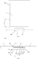
- FIG. 1 is a perspective view of an electronic apparatus 100 shown in a first viewing angle.
- the electronic apparatus 100 may include a cover assembly 1 and a fingerprint button 2.
- the cover assembly 1 may define a receiving hole 20, and the fingerprint button 2 may be received in the receiving hole 20.
- the receiving hole 20 defined in the cover assembly 1 and the fingerprint button 2 may together form a light-emitting prompting device 200.
- the fingerprint button 2 may include a fingerprint recognition device 31 and a light-emitting portion 32.
- the fingerprint identification device 31 may include a fingerprint chip 311, a circuit board 312, and a fingerprint cover 313.
- the circuit board 312, the fingerprint chip 311, and the fingerprint cover 313 may be successively stacked on the light-emitting portion 32.
- the circuit board 312 may be located at one side that is close to the light-emitting portion 32, and may be configured to carry the fingerprint chip 311.
- the fingerprint cover 313 may be located at one side that is away from the light-emitting portion 32, and may be configured to protect the fingerprint chip 311.
- the fingerprint cover 313 may include an ITO (Indium Tin Oxid) transparent film, and may be conductive.
- the fingerprint chip 311 may be configured to detect a touch from a user, collect fingerprint information when the user touches the electronic apparatus, perform feature extraction and feature comparison based on the fingerprint information, and determine whether the collected fingerprint information matches with pre-stored fingerprint information.
- the circuit board 312 may be configured to carry the fingerprint chip 311 and other functional chips.
- the circuit board 312 may also carry a power chip configured to supply power to the fingerprint chip 311.
- the fingerprint chip 311 may be packaged by means of BGA (Ball Grid Array) technology or by means of LGA (Land Grid Array) technology.
- the fingerprint cover 313 may define a light-shielding region 314 and a light-transmitting region 315.
- the fingerprint chip 311 may be located at a position below the fingerprint cover 313 and corresponding to the light-shielding region 314.
- the circuit board 312 may be configured to carry the fingerprint chip 311, and may be located below the fingerprint chip 311 and corresponding to the light-shielding region 314. That is, in this embodiment, a size of the fingerprint cover 313 may be greater than sizes respectively of the fingerprint chip 311 and the circuit board 312, and projections respectively of the fingerprint chip 311 and the circuit board 312 on the fingerprint cover 313 may be substantially located in the light-shielding region 314.
- the light-emitting portion 32 may be located below the circuit board 312 of the fingerprint recognition device 31, and further extend beyond the circuit board 312 of the fingerprint recognition device 31. A part of the light-emitting portion 32 extending beyond the circuit board 312 of the fingerprint recognition device 31 may be located below the light-transmitting region 315, such that the light-emitting portion 32 may cover the light-transmitting region 315 from the inner side of the cover assembly 1.
- an inner surface N1 of the fingerprint cover 313 may be covered with an ink layer Y1, and the light-transmitting region Y may be formed by removing the ink in a preset region on the inner surface N1 of the fingerprint cover 313.
- the light-transmitting region Y is namely the preset region which is not covered by the ink.
- the light-shielding region 314 may be a region in which the inner surface N1 of the fingerprint cover 313 is covered by the ink layer Y1.
- FIG. 3 is a schematic view of the inner surface N1 of the fingerprint cover 313.
- the light-shielding region 314 may be located at a middle of the fingerprint cover 313, and the light-transmitting region 315 and the preset region may be the region that is close to an edge of the fingerprint cover 313.
- the light-transmitting region 315 and the preset region may be an annular region surrounding the light-shielding region 314. As shown in FIG.
- the fingerprint cover 313 and the light-shielding region 314 may be in shape of an ellipse, and the light-transmitting region 315 may be the annular region in shape of an ellipse and surrounding the light-shielding region 314.
- the receiving hole 20 may also be in shape of an ellipse, and the fingerprint cover 313 and the receiving hole 20 may be substantially equal in size. In this way, after the fingerprint cover 313 is received in the receiving hole 20, the fingerprint cover 313 may be closely attached to a side wall of the receiving hole 20.
- the fingerprint cover 313 and the light-shielding region 314 may be in shape of a square, and the light-transmitting region 315 may be an annular region in shape of a square, adjacent to and surrounding the light-shielding region 314.
- the light-transmitting region 315 may also be one or more strip regions adjacent to one or more edges of the light-shielding region 314.
- the cover assembly 1 may be a front cover.
- the cover assembly 1 may further include a frame 11 and a screen receiving area 12.
- the receiving hole 20 may be defined in a lower region of the frame 11.
- the electronic apparatus 100 may further include a screen 3 that is received in the screen receiving area 12 of the cover assembly 1.
- the screen 3 may be a touch screen.
- the cover assembly 1 may include transparent glass, transparent resin, metal, plastic, or the like.
- a preset event may be a fingerprint touch event.
- the light-emitting unit 32 may emit lights when the fingerprint chip 311 detects a touch from the user, thereby prompting that the touch from the user initiates the fingerprint recognition function.
- the light-emitting portion 32 may include a light-guiding plate 321 and a light source 322.
- the light-guiding plate 321 may be disposed below the circuit board 312 of the fingerprint recognition device 31, extend beyond the circuit board 31 of the fingerprint recognition device 31, and further shield the light-transmitting region 315.
- the light source 322 may be disposed close to the light-guiding plate 321. When the light source 322 emits lights, the light-guiding plate 321 may guide the lights emitted from the light source 322 to the light-transmitting region 315. The emitted lights may be further emitted out of fingerprint cover 313 via the light-transmitting region 315, and served as a prompt.
- the light source 322 may be disposed at a side wall C1 of the light-guiding plate 321.
- the light source 322 may be disposed on a bottom surface D1 of the light-guiding plate 321 that is away from the fingerprint recognition device 31.
- the light-emitting portion 32 may include only the light source 322 disposed below the fingerprint recognition device 31 and extending beyond the fingerprint recognition device 31; the light source 322 may further extend below the light-transmitting region 315.
- the light source 322 may emit lights in response to the preset event, and the lights may be further emitted out of the cover assembly 1 via the light-transmitting region 315, in order to prompt the preset event. More specifically, the light source 322 may be disposed below the circuit board 312, and extend beyond the circuit board 312. The light source 322 may further extend below the light-transmitting region 315.
- the light source 322 described above may be an LED lamp group including one LED lamp or a plurality of LED lamps.
- the LED lamp or the LED lamp group may emit lights in white, red, green, yellow, or the like.
- the light-guiding plate 321 may include materials such as transparent glass, transparent resin, transparent plastic, or the like.
- FIG. 6 is a block diagram showing the structure of some components of the electronic apparatus 100.
- the electronic apparatus 100 may include the fingerprint button 2 and the screen 3 described above.
- the electronic apparatus 100 may further include a processor 4 and a power supply circuit 5.
- the power supply circuit 5 may be connected to the light source 322 of the light-emitting unit 32, and configured to supply power to the light source 322. As shown in FIG. 6 , the power supply circuit 5 may include a power source 51 and a power switch 52. The power switch 52 may be connected between the power source 51 and the light source 322. The processor 4 may be configured to turn on the power switch 52 when the preset event occurs, such that the power source 51 is capable of supplying power to the light source 322.
- the light source 322 may emit lights. The emitted lights may be guided to the gap via the light-guiding plate 321, and further emitted out of the electronic apparatus from the light-transmitting region 315. The emitted lights may be served as a prompt.
- the power source 51 may be a battery.
- the preset event may be a fingerprint touch event.
- the processor 4 may be connected to the fingerprint chip 311 of the fingerprint recognition device 31 of the fingerprint button 2, and configured to turn on the power switch 52 when the fingerprint chip 311 detects a touch from the user, such that the power source 51 is capable of supplying power to the light source 322.
- the light source 322 may be electrically illuminated and emit lights, and the emitted lights may be emitted out of the electronic apparatus via the light-transmitting region 315.
- the light source 322 may emit lights; the emitted lights may be guided to the light-transmitting region 315 via the light-guiding plate 321 and further emitted out of the electronic apparatus from the light-transmitting region 315 for prompting.
- the lights emitted from the light source 322 may be directly transmitted to the light-transmitting region 315, and further emitted out of the electronic apparatus from the light-transmitting region 315 for prompting.
- the light source 322 may be operated in a continuous illumination mode or a flickering illumination mode.
- the processor 4 may continuously turn on the power switch 52, such that the light source 322 may continuously emit lights, that is, the light source 322 may perform a constant-on illumination.
- the processor 4 may alternately turn on and off the power switch 52, such that the light source 322 may emit lights and stop emitting lights alternately, that is, the light source 322 may perform a flickering illumination.
- the power switch 52 may be a MOS transistor Q1.
- a drain electrode of the MOS transistor Q1 may be connected to the power source 51, a source electrode of the MOS transistor Q1 may be connected to the light source 322, and a gate electrode of the MOS transistor Q1 may be connected to the processor 4.
- the processor 4 may be configured to generate a corresponding level signal to turn on or off the MOS transistor Q1, such that the power source 51 may correspondingly supply power to or stop supplying power to the light source 322, and thus the light source 322 may be powered on and emit lights, or the light source 322 may be powered off and stop emitting lights.
- the power switch 52 may be an N-type MOS transistor Q1, and the processor 4 may be configured to generate a high level signal, and further send the high level signal to the MOS transistor Q1, in order to turn on control the MOS transistor Q1.
- the processor 4 may also be configured to generate a low level signal, and further send the low level signal to the MOS transistor Q1, in order to turn off the MOS transistor Q1.
- the processor 4 may be configured to continuously generate and send high level signals to the MOS transistor Q1 to continuously turn on control the MOS transistor Q1. In this way, the light source 322 is continuously supplied with power, and thus the light source 322 may continuously emit lights.
- the processor 4 may be configured to generate and send high level signals and low level signals alternately to the MOS transistor Q1 to alternately turn on and off the MOS transistor Q1. In this way, the light source 322 may be alternately powered on or powered off, and thus the light source 322 may flickeringly emits lights.
- the power switch may be a triode, an IGBT tube, or the like.
- the preset event may further include an incoming call event or a missed call event, an unread short message event, a schedule reminding event, or the like.
- the processor 4 may be further configured to generate and send a corresponding level signal to the power switch 52 to turn on the power switch 52, such that the power source 51 may supply power to the light source 322.
- the light source 322 may emit lights.
- the emitted lights may be guided to the light-transmitting region 315 via the light-guiding plate 321, or may be directly transmitted to the light-transmitting region 315 and further emitted out of the electronic apparatus from the light-transmitting region 315 for prompting.
- the cover assembly 1 may also be a rear cover of the electronic apparatus 100.
- the receiving hole 20 may be defined in the rear cover, and the fingerprint button 2 may be received in the receiving hole 20 defined in the rear cover.
- the electronic apparatus 1 may be a mobile phone, a tablet computer, a PDA (personal digital assistant), a sales terminal POS, a car computer, or the like.
- the processor 4 may control the light source 322 of the light-emitting portion 32 to emit lights, in order to generate a corresponding prompt.
- the light-emitting prompting device 200 and the electronic apparatus 100 of the present disclosure may realize the functions of fingerprint button and the prompting in the region disposing the fingerprint button 2 at the same time. In this way, it is unnecessary to additionally provide a prompting device such as a prompting light in other places of the housing, thereby saving design space.
Landscapes
- Engineering & Computer Science (AREA)
- Physics & Mathematics (AREA)
- General Physics & Mathematics (AREA)
- General Engineering & Computer Science (AREA)
- Multimedia (AREA)
- Theoretical Computer Science (AREA)
- Human Computer Interaction (AREA)
- Health & Medical Sciences (AREA)
- General Health & Medical Sciences (AREA)
- Vascular Medicine (AREA)
- Optics & Photonics (AREA)
- Image Input (AREA)
- Telephone Set Structure (AREA)
Abstract
Description
- The described embodiments relate to electronic apparatuses, and in particular to a fingerprint button, a light-emitting prompting device, and an electronic apparatus having the light-emitting prompting device.
- At present, electronic apparatuses, such as mobile phones and computers, have been widely used as communication and information interaction devices. Users can make phone calls, send short messages, or connect with others through social software by using the electronic apparatuses, which bringing lots of convenience to the users in their daily lives. In order to prompt incoming calls, short messages or other events, the electronic apparatuses are usually equipped with prompting lights to perform visual promptings. For example, when there are unread short messages, the prompting lights will be illuminated to prompt the user.
- However, the prompting lights in the related art are separately disposed on front screens of the electronic apparatuses, and the prompting lights occupy extra space. In this way, for an electronic apparatus having a smaller volume such as a mobile phone or the like, the screen ratio is further reduced.
- In view of this, the present disclosure provides a fingerprint button, a light-emitting prompting device, and an electronic apparatus.
- In one aspect, a fingerprint button is provided. The fingerprint button may include a fingerprint recognition device and a light-emitting portion. The fingerprint recognition device may include: a fingerprint cover defining a light-shielding region and a light-transmitting region; a fingerprint chip, located at a position below the fingerprint cover and corresponding to the light-shielding region; and a circuit board, configured to carry the fingerprint chip, and located at a position below the fingerprint chip and corresponding to the light-shielding region. Wherein the light-emitting portion is located below the circuit board of the fingerprint identification device and extends beyond the circuit board of the fingerprint recognition device; a part of the light-emitting portion extending beyond the circuit board of the fingerprint identification device is located below the light-transmitting region, such that the light-emitting portion covers the light-transmitting region from an inner side of a cover assembly.
- In another aspect, a light-emitting prompting device may be provided. The light-emitting prompting device may be arranged on an electronic apparatus. The light-emitting prompting device may include a receiving hole defined in a cover assembly of the electronic apparatus, and further include the fingerprint button described above. The fingerprint button is received in the receiving hole.
- In a further aspect, an electronic apparatus is provided. The electronic apparatus may include a cover assembly and a fingerprint button. The cover assembly may define a receiving hole. The fingerprint button may include a fingerprint identification device and a light-emitting portion, and the fingerprint recognition device may be received in the receiving hole. The fingerprint identification device may include a fingerprint recognition device and a light-emitting portion. The fingerprint recognition device may include: a fingerprint cover, defining a light-shielding region and a light-transmitting region; a fingerprint chip, located at a position below the fingerprint cover and corresponding to the light-shielding region; and a circuit board, configured to carry the fingerprint chip, and located at a position below the fingerprint chip and corresponding to the light-shielding region. Wherein the light-emitting portion is located below the circuit board of the fingerprint identification device and extends beyond the circuit board of the fingerprint recognition device; a part of the light-emitting portion extending beyond the circuit board of the fingerprint identification device is located below the light-transmitting region, such that the light-emitting portion covers the light-transmitting region from an inner side of a cover assembly.
- The fingerprint button, the light-emitting prompting device and the electronic apparatus of the present disclosure may realize the functions of fingerprint button and the prompting in the region disposing the fingerprint button at the same time. In this way, it is unnecessary to additionally provide a prompting device such as a prompting light in other places of the housing, thereby saving design space.
- In order to make the technical solutions described in the embodiments of the present disclosure or the technical solution in the related art more clear, the drawings used for the description of the embodiments or the related art will be briefly described. Apparently, the drawings described below are only some of the embodiments of the present disclosure, and those skilled in the art may acquire other drawings based on these drawings, without making any creative efforts.
-
FIG. 1 is a perspective view of an electronic apparatus shown in a first viewing angle according to an embodiment of the present disclosure. -
FIG. 2 is a cross-sectional view of the electronic apparatus taken along line II-II ofFIG. 1 according to a first embodiment of the present disclosure. -
FIG. 3 is a schematic view of an inner surface of a fingerprint cover of the electronic apparatus according to an embodiment of the present disclosure. -
FIG. 4 is a cross-sectional view of the electronic apparatus taken along line II-II ofFIG. 1 according to a second embodiment of the present disclosure. -
FIG. 5 is a cross-sectional view of the electronic apparatus taken along line II-II ofFIG. 1 according to a third embodiment of the present disclosure. -
FIG. 6 is a block diagram showing the structure of some components of the electronic apparatus according to an embodiment of the present disclosure. - Technical solutions in the embodiments of the present disclosure will be clearly and completely described below with reference to the accompanying drawings in the embodiments of the present disclosure. Apparently, the embodiments described below are merely some of the embodiments of the present disclosure, rather than all of the embodiments. All other embodiments obtained by those skilled in the art without creative efforts on the basis of the embodiments of the present disclosure shall fall within the protection scope of the present disclosure.
Referring toFIG. 1 and FIG. 2, FIG. 1 is a perspective view of anelectronic apparatus 100 shown in a first viewing angle. Theelectronic apparatus 100 may include acover assembly 1 and afingerprint button 2. In this case, thecover assembly 1 may define a receivinghole 20, and thefingerprint button 2 may be received in the receivinghole 20. Thereceiving hole 20 defined in thecover assembly 1 and thefingerprint button 2 may together form a light-emittingprompting device 200. - As shown in
FIG. 2 , thefingerprint button 2 may include afingerprint recognition device 31 and a light-emittingportion 32. Thefingerprint identification device 31 may include afingerprint chip 311, acircuit board 312, and afingerprint cover 313. Thecircuit board 312, thefingerprint chip 311, and thefingerprint cover 313 may be successively stacked on the light-emittingportion 32. Thecircuit board 312 may be located at one side that is close to the light-emittingportion 32, and may be configured to carry thefingerprint chip 311. Thefingerprint cover 313 may be located at one side that is away from the light-emittingportion 32, and may be configured to protect thefingerprint chip 311. Thefingerprint cover 313 may include an ITO (Indium Tin Oxid) transparent film, and may be conductive. Thefingerprint chip 311 may be configured to detect a touch from a user, collect fingerprint information when the user touches the electronic apparatus, perform feature extraction and feature comparison based on the fingerprint information, and determine whether the collected fingerprint information matches with pre-stored fingerprint information. Thecircuit board 312 may be configured to carry thefingerprint chip 311 and other functional chips. For example, thecircuit board 312 may also carry a power chip configured to supply power to thefingerprint chip 311. Thefingerprint chip 311 may be packaged by means of BGA (Ball Grid Array) technology or by means of LGA (Land Grid Array) technology. - In this case, the
fingerprint cover 313 may define a light-shielding region 314 and a light-transmittingregion 315. Thefingerprint chip 311 may be located at a position below thefingerprint cover 313 and corresponding to the light-shielding region 314. Thecircuit board 312 may be configured to carry thefingerprint chip 311, and may be located below thefingerprint chip 311 and corresponding to the light-shielding region 314. That is, in this embodiment, a size of thefingerprint cover 313 may be greater than sizes respectively of thefingerprint chip 311 and thecircuit board 312, and projections respectively of thefingerprint chip 311 and thecircuit board 312 on thefingerprint cover 313 may be substantially located in the light-shielding region 314. - The light-
emitting portion 32 may be located below thecircuit board 312 of thefingerprint recognition device 31, and further extend beyond thecircuit board 312 of thefingerprint recognition device 31. A part of the light-emittingportion 32 extending beyond thecircuit board 312 of thefingerprint recognition device 31 may be located below the light-transmittingregion 315, such that the light-emittingportion 32 may cover the light-transmittingregion 315 from the inner side of thecover assembly 1. - As shown in
FIG. 2 , an inner surface N1 of thefingerprint cover 313 may be covered with an ink layer Y1, and the light-transmitting region Y may be formed by removing the ink in a preset region on the inner surface N1 of thefingerprint cover 313. Thus, the light-transmitting region Y is namely the preset region which is not covered by the ink. The light-shielding region 314 may be a region in which the inner surface N1 of thefingerprint cover 313 is covered by the ink layer Y1. - Referring to
FIG. 3, FIG. 3 is a schematic view of the inner surface N1 of thefingerprint cover 313. In some embodiments, the light-shieldingregion 314 may be located at a middle of thefingerprint cover 313, and the light-transmittingregion 315 and the preset region may be the region that is close to an edge of thefingerprint cover 313. For example, the light-transmittingregion 315 and the preset region may be an annular region surrounding the light-shieldingregion 314. As shown inFIG. 3 , in some embodiments, thefingerprint cover 313 and the light-shieldingregion 314 may be in shape of an ellipse, and the light-transmittingregion 315 may be the annular region in shape of an ellipse and surrounding the light-shieldingregion 314. As shown inFIG. 1 and FIG. 2 , in some embodiments, the receivinghole 20 may also be in shape of an ellipse, and thefingerprint cover 313 and the receivinghole 20 may be substantially equal in size. In this way, after thefingerprint cover 313 is received in the receivinghole 20, thefingerprint cover 313 may be closely attached to a side wall of the receivinghole 20. In other embodiments, thefingerprint cover 313 and the light-shieldingregion 314 may be in shape of a square, and the light-transmittingregion 315 may be an annular region in shape of a square, adjacent to and surrounding the light-shieldingregion 314. Optionally, the light-transmittingregion 315 may also be one or more strip regions adjacent to one or more edges of the light-shieldingregion 314. - As shown in
FIG. 1 , in some embodiments, thecover assembly 1 may be a front cover. Thecover assembly 1 may further include aframe 11 and ascreen receiving area 12. The receivinghole 20 may be defined in a lower region of theframe 11. Theelectronic apparatus 100 may further include ascreen 3 that is received in thescreen receiving area 12 of thecover assembly 1. Thescreen 3 may be a touch screen. - In some embodiments, the
cover assembly 1 may include transparent glass, transparent resin, metal, plastic, or the like. - In some embodiments, a preset event may be a fingerprint touch event. The light-emitting
unit 32 may emit lights when thefingerprint chip 311 detects a touch from the user, thereby prompting that the touch from the user initiates the fingerprint recognition function. - As shown in
FIG. 2 , in some embodiments, the light-emittingportion 32 may include a light-guidingplate 321 and alight source 322. The light-guidingplate 321 may be disposed below thecircuit board 312 of thefingerprint recognition device 31, extend beyond thecircuit board 31 of thefingerprint recognition device 31, and further shield the light-transmittingregion 315. Thelight source 322 may be disposed close to the light-guidingplate 321. When thelight source 322 emits lights, the light-guidingplate 321 may guide the lights emitted from thelight source 322 to the light-transmittingregion 315. The emitted lights may be further emitted out offingerprint cover 313 via the light-transmittingregion 315, and served as a prompt. - As shown in
FIG. 2 , in some embodiments, thelight source 322 may be disposed at a side wall C1 of the light-guidingplate 321. - Referring to
FIG. 4 , in other embodiments, thelight source 322 may be disposed on a bottom surface D1 of the light-guidingplate 321 that is away from thefingerprint recognition device 31. - Referring to
FIG. 5 , in other embodiments, the light-emittingportion 32 may include only thelight source 322 disposed below thefingerprint recognition device 31 and extending beyond thefingerprint recognition device 31; thelight source 322 may further extend below the light-transmittingregion 315. Thelight source 322 may emit lights in response to the preset event, and the lights may be further emitted out of thecover assembly 1 via the light-transmittingregion 315, in order to prompt the preset event. More specifically, thelight source 322 may be disposed below thecircuit board 312, and extend beyond thecircuit board 312. Thelight source 322 may further extend below the light-transmittingregion 315. - In some embodiments, the
light source 322 described above may be an LED lamp group including one LED lamp or a plurality of LED lamps. The LED lamp or the LED lamp group may emit lights in white, red, green, yellow, or the like. The light-guidingplate 321 may include materials such as transparent glass, transparent resin, transparent plastic, or the like. - Referring to
FIG. 6, FIG. 6 is a block diagram showing the structure of some components of theelectronic apparatus 100. Theelectronic apparatus 100 may include thefingerprint button 2 and thescreen 3 described above. Theelectronic apparatus 100 may further include aprocessor 4 and apower supply circuit 5. - The
power supply circuit 5 may be connected to thelight source 322 of the light-emittingunit 32, and configured to supply power to thelight source 322. As shown inFIG. 6 , thepower supply circuit 5 may include apower source 51 and apower switch 52. Thepower switch 52 may be connected between thepower source 51 and thelight source 322. Theprocessor 4 may be configured to turn on thepower switch 52 when the preset event occurs, such that thepower source 51 is capable of supplying power to thelight source 322. Thelight source 322 may emit lights. The emitted lights may be guided to the gap via the light-guidingplate 321, and further emitted out of the electronic apparatus from the light-transmittingregion 315. The emitted lights may be served as a prompt. - In this case, the
power source 51 may be a battery. - As described above, in some embodiments, the preset event may be a fingerprint touch event. The
processor 4 may be connected to thefingerprint chip 311 of thefingerprint recognition device 31 of thefingerprint button 2, and configured to turn on thepower switch 52 when thefingerprint chip 311 detects a touch from the user, such that thepower source 51 is capable of supplying power to thelight source 322. At this time, thelight source 322 may be electrically illuminated and emit lights, and the emitted lights may be emitted out of the electronic apparatus via the light-transmittingregion 315. When the light-emittingportion 32 includes thelight source 322 and the light-guidingplate 321, thelight source 322 may emit lights; the emitted lights may be guided to the light-transmittingregion 315 via the light-guidingplate 321 and further emitted out of the electronic apparatus from the light-transmittingregion 315 for prompting. When the light-emittingportion 32 includes only the light source, the lights emitted from thelight source 322 may be directly transmitted to the light-transmittingregion 315, and further emitted out of the electronic apparatus from the light-transmittingregion 315 for prompting. - As described above, the
light source 322 may be operated in a continuous illumination mode or a flickering illumination mode. In one embodiment, theprocessor 4 may continuously turn on thepower switch 52, such that thelight source 322 may continuously emit lights, that is, thelight source 322 may perform a constant-on illumination. In another embodiment, theprocessor 4 may alternately turn on and off thepower switch 52, such that thelight source 322 may emit lights and stop emitting lights alternately, that is, thelight source 322 may perform a flickering illumination. - As shown in
FIG. 6 , in some embodiments, thepower switch 52 may be a MOS transistor Q1. A drain electrode of the MOS transistor Q1 may be connected to thepower source 51, a source electrode of the MOS transistor Q1 may be connected to thelight source 322, and a gate electrode of the MOS transistor Q1 may be connected to theprocessor 4. Theprocessor 4 may be configured to generate a corresponding level signal to turn on or off the MOS transistor Q1, such that thepower source 51 may correspondingly supply power to or stop supplying power to thelight source 322, and thus thelight source 322 may be powered on and emit lights, or thelight source 322 may be powered off and stop emitting lights. More specifically, thepower switch 52 may be an N-type MOS transistor Q1, and theprocessor 4 may be configured to generate a high level signal, and further send the high level signal to the MOS transistor Q1, in order to turn on control the MOS transistor Q1. Theprocessor 4 may also be configured to generate a low level signal, and further send the low level signal to the MOS transistor Q1, in order to turn off the MOS transistor Q1. When thelight source 322 is in the continuous illumination mode, theprocessor 4 may be configured to continuously generate and send high level signals to the MOS transistor Q1 to continuously turn on control the MOS transistor Q1. In this way, thelight source 322 is continuously supplied with power, and thus thelight source 322 may continuously emit lights. When thelight source 322 is in the flickering illumination mode, theprocessor 4 may be configured to generate and send high level signals and low level signals alternately to the MOS transistor Q1 to alternately turn on and off the MOS transistor Q1. In this way, thelight source 322 may be alternately powered on or powered off, and thus thelight source 322 may flickeringly emits lights. - In other embodiments, the power switch may be a triode, an IGBT tube, or the like.
- In some embodiments, the preset event may further include an incoming call event or a missed call event, an unread short message event, a schedule reminding event, or the like. When an event such as an incoming call event or a missed call event, an unread short message event, a schedule reminding event, or the like occurs, the
processor 4 may be further configured to generate and send a corresponding level signal to thepower switch 52 to turn on thepower switch 52, such that thepower source 51 may supply power to thelight source 322. Thelight source 322 may emit lights. The emitted lights may be guided to the light-transmittingregion 315 via the light-guidingplate 321, or may be directly transmitted to the light-transmittingregion 315 and further emitted out of the electronic apparatus from the light-transmittingregion 315 for prompting. - In some embodiments, the
cover assembly 1 may also be a rear cover of theelectronic apparatus 100. The receivinghole 20 may be defined in the rear cover, and thefingerprint button 2 may be received in the receivinghole 20 defined in the rear cover. - In some embodiments, the
electronic apparatus 1 may be a mobile phone, a tablet computer, a PDA (personal digital assistant), a sales terminal POS, a car computer, or the like. - Therefore, in the present disclosure, when an event such as an incoming call event or missed call event, an unread short message event, a schedule reminding event, a fingerprint touch event, a button press event, or the like occurs, the
processor 4 may control thelight source 322 of the light-emittingportion 32 to emit lights, in order to generate a corresponding prompt. - The light-emitting
prompting device 200 and theelectronic apparatus 100 of the present disclosure may realize the functions of fingerprint button and the prompting in the region disposing thefingerprint button 2 at the same time. In this way, it is unnecessary to additionally provide a prompting device such as a prompting light in other places of the housing, thereby saving design space. - The above is only some embodiments of the present disclosure, and the protection scope of the present disclosure should not be limited thereto. Those skilled in the art may understand all or parts of the processes for implementing the above embodiments, and make equivalents and modifications based on the claims of the present disclosure. All these shall be covered within the scope of the invention.
Claims (20)
- A fingerprint button, comprising a fingerprint recognition device and a light-emitting portion, wherein the fingerprint recognition device comprises:a fingerprint cover, defining a light-shielding region and a light-transmitting region;a fingerprint chip, located at a position below the fingerprint cover and corresponding to the light-shielding region; anda circuit board, configured to carry the fingerprint chip, and located at a position below the fingerprint chip and corresponding to the light-shielding region;wherein the light-emitting portion is located below the circuit board of the fingerprint identification device and extends beyond the circuit board of the fingerprint recognition device; a part of the light-emitting portion extending beyond the circuit board of the fingerprint identification device is located below the light-transmitting region, such that the light-emitting portion shields the light-transmitting region from an inner side of a cover assembly.
- The fingerprint button of claim 1, wherein an inner surface of the fingerprint cover is covered with an ink layer, and the light-transmitting region is formed by removing the ink in a preset region on the inner surface of the fingerprint cover; the light-shielding region is a region in which the inner surface of the fingerprint cover is covered by the ink layer.
- The fingerprint button of claim 2, wherein the light-shielding region is located at a middle of the fingerprint cover, and the light-transmitting region is the region close to an edge of the fingerprint cover.
- The fingerprint button of claim 3, wherein the light-emitting portion comprises a light-guiding plate and a light source; the light-guiding plate is disposed below the circuit board, extends beyond the circuit board, and further shields the light-transmitting region; the light source is disposed close to the light-guiding plate; the light source emits lights in response to a preset event; the lights emitted from the light source are guided to the light-transmitting region via the light-guiding plate, and further emitted out of the fingerprint cover to prompt the preset event.
- The fingerprint button of claim 3, wherein the light-emitting portion comprises a light source disposed below the circuit board, extending beyond the circuit board, and further extending below the light-transmitting region; the light source emits lights in response to a preset event; the lights emitted from the light source are further emitted out of the fingerprint cover via the light-transmitting region to prompt the preset event.
- The fingerprint button of claims 4 or 5, wherein the light source is an LED lamp group comprising one LED lamp or a plurality of LED lamps, and the LED lamp or the LED lamp group emits lights in white or in colors.
- The fingerprint button of any one of claims 1-6, wherein the fingerprint chip is packaged by means of ball grid array technology or by means of land grid array technology.
- A light-emitting prompting device, arranged on an electronic apparatus; wherein the light-emitting prompting device comprises a receiving hole defined in a cover assembly of the electronic apparatus, and further comprises the fingerprint button of claims 1-7; the fingerprint button is received in the receiving hole.
- An electronic apparatus, comprising a cover assembly and a fingerprint button; the cover assembly defining a receiving hole; the fingerprint button comprising a fingerprint identification device and a light-emitting portion, and the fingerprint recognition device being received in the receiving hole; the fingerprint identification device comprising:a fingerprint cover, defining a light-shielding region and a light-transmitting region;a fingerprint chip, located at a position below the fingerprint cover and corresponding to the light-shielding region; anda circuit board, configured to carry the fingerprint chip, and located at a position below the fingerprint chip and corresponding to the light-shielding region;wherein the light-emitting portion is located below the circuit board of the fingerprint identification device and extends beyond the circuit board of the fingerprint recognition device; a part of the light-emitting portion extending beyond the circuit board of the fingerprint identification device is located below the light-transmitting region, such that the light-emitting portion shields the light-transmitting region from an inner side of a cover assembly.
- The electronic apparatus of claim 9, wherein an inner surface of the fingerprint cover is covered with an ink layer, and the light-transmitting region is formed by removing the ink in a preset region on the inner surface of the fingerprint cover; the light-shielding region is a region in which the inner surface of the fingerprint cover is covered by the ink layer.
- The electronic apparatus of claim 10, wherein the light-shielding region is located at a middle of the fingerprint cover, and the light-transmitting region is the region close to an edge of the fingerprint cover.
- The electronic device of claim 11, wherein the light-emitting portion comprises a light-guiding plate and a light source; the light-guiding plate is disposed below the circuit board, extends beyond the circuit board, and further shields the light-transmitting region; the light source is disposed close to the light-guiding plate; the light source emits lights in response to a preset event; the lights emitted from the light source are guided to the light-transmitting region via the light-guiding plate, and further emitted out of the fingerprint cover to prompt the preset event.
- The electronic apparatus of claim 11, wherein the light-emitting portion comprises a light source disposed below the circuit board, extending beyond the circuit board, and further extending below the light-transmitting region; the light source emits lights in response to a preset event; the lights emitted from the light source are further emitted out of the fingerprint cover via the light-transmitting region to prompt the preset event.
- The electronic apparatus of claims 12 or 13, wherein the light source is an LED lamp group comprising one LED lamp or a plurality of LED lamps, and the LED lamp or the LED lamp group emits lights in white or in colors.
- The electronic apparatus of claims 12 or 13, wherein the electronic apparatus further comprises:a power supply circuit, connected to a light source of the light-emitting portion and configured to supply power to the light source; wherein the power supply circuit comprises a power source and a power switch, and the power switch is connected between the power source and the light source; anda processor, configured to turn on the power switch when the preset event occurs, such that the power source is capable of supplying power to the light source, and the light source emits lights; the lights emitted from the light are emitted out of the electronic apparatus via the light-transmitting region for prompting.
- The electronic apparatus of claim 15, wherein the preset event is a fingerprint touch event; the processor is further connected to the fingerprint chip of the fingerprint recognition device, and configured to turn on the power switch when a touch from a user is detected by the fingerprint chip, such that the power source is capable of supplying power to the light source, and the light source is electrically illuminated and emits lights; the emitted lights are emitted out of the electronic apparatus via the light-transmitting region.
- The electronic apparatus of claims 15 or 16, wherein the processor is configured to continuously turn on the power switch, such that the light source continuously emits lights; or the processor is configured to alternately turn on and off the power switch, such that the light source flickeringly emits lights.
- The electronic apparatus of any one of claims 15-17, wherein the power switch is a MOS transistor; a drain electrode of the MOS transistor is connected to the power source, a source electrode of the MOS transistor is connected to the light source, and a gate electrode of the MOS transistor is connected to the processor; the processor is configured to generate a corresponding level signal to turn on or off the MOS transistor.
- The electronic apparatus of any one of claims 11-18, wherein the cover assembly is a front cover or a rear cover of the electronic apparatus.
- The electronic apparatus of any one of claims 11-18, wherein the fingerprint chip is packaged by means of ball grid array technology or by means of land grid array technology.
Applications Claiming Priority (2)
| Application Number | Priority Date | Filing Date | Title |
|---|---|---|---|
| CN201620877540.2U CN206178863U (en) | 2016-08-12 | 2016-08-12 | Fingerprint button, luminous suggestion structure and terminal equipment |
| PCT/CN2017/091876 WO2018028356A1 (en) | 2016-08-12 | 2017-07-05 | Fingerprint button, light-emitting prompt structure, and terminal device |
Publications (2)
| Publication Number | Publication Date |
|---|---|
| EP3460713A1 true EP3460713A1 (en) | 2019-03-27 |
| EP3460713A4 EP3460713A4 (en) | 2019-08-14 |
Family
ID=60240901
Family Applications (1)
| Application Number | Title | Priority Date | Filing Date |
|---|---|---|---|
| EP17838486.3A Ceased EP3460713A4 (en) | 2016-08-12 | 2017-07-05 | DIGITAL FOOTPRINT BUTTON, LIGHT EMITTING GUEST STRUCTURE, AND TERMINAL DEVICE |
Country Status (4)
| Country | Link |
|---|---|
| US (1) | US10876722B2 (en) |
| EP (1) | EP3460713A4 (en) |
| CN (1) | CN206178863U (en) |
| WO (1) | WO2018028356A1 (en) |
Families Citing this family (4)
| Publication number | Priority date | Publication date | Assignee | Title |
|---|---|---|---|---|
| TWI630502B (en) * | 2016-08-05 | 2018-07-21 | 金佶科技股份有限公司 | Image capture apparatus |
| CN206178863U (en) * | 2016-08-12 | 2017-05-17 | 广东欧珀移动通信有限公司 | Fingerprint button, luminous suggestion structure and terminal equipment |
| CN108280336A (en) * | 2018-01-19 | 2018-07-13 | 京东方科技集团股份有限公司 | Unlocked by fingerprint method and unlocked by fingerprint device |
| CN111430170B (en) * | 2020-03-20 | 2022-08-05 | 惠州Tcl移动通信有限公司 | Key and processing method thereof and mobile terminal |
Family Cites Families (17)
| Publication number | Priority date | Publication date | Assignee | Title |
|---|---|---|---|---|
| JP3733357B2 (en) * | 2003-05-28 | 2006-01-11 | キヤノン株式会社 | Fingerprint input device and personal authentication system using the same |
| US7515252B2 (en) * | 2005-12-30 | 2009-04-07 | Cardinal Health 303, Inc. | Optical fingerprint imaging system and method with protective film |
| CN202075693U (en) | 2011-02-11 | 2011-12-14 | 叶昇 | Information input device with luminescence prompting function |
| TWI444904B (en) * | 2011-06-24 | 2014-07-11 | Gingy Technology Inc | Finger print identification device |
| AU2013100571A4 (en) * | 2012-05-18 | 2013-05-23 | Apple Inc. | Capacitive sensor packaging |
| CN103942559A (en) * | 2013-01-21 | 2014-07-23 | 义明科技股份有限公司 | Image sensing device and decoding circuit thereof |
| EP3072083B1 (en) * | 2013-11-22 | 2018-07-18 | Shenzhen Goodix Technology Co., Ltd. | Secure human fingerprint sensor |
| US9886613B2 (en) * | 2014-07-07 | 2018-02-06 | Shenzhen GOODIX Technology Co., Ltd. | Integration of touch screen and fingerprint sensor assembly |
| US9576177B2 (en) * | 2014-12-11 | 2017-02-21 | Fingerprint Cards Ab | Fingerprint sensing device |
| CN104598893A (en) * | 2015-02-03 | 2015-05-06 | 上海箩箕技术有限公司 | Fingerprint recognition system, running method of fingerprint recognition system and electronic product |
| CN104700080A (en) * | 2015-03-06 | 2015-06-10 | 南昌欧菲生物识别技术有限公司 | Fingerprint recognition module and touch screen based on fingerprint recognition |
| CN204791058U (en) * | 2015-07-09 | 2015-11-18 | 广东欧珀移动通信有限公司 | Fingerprint identification device and have this fingerprint identification device's terminal |
| CN205334501U (en) * | 2016-01-18 | 2016-06-22 | 宸盛光电有限公司 | Fingerprint identification device and electronic equipment with the fingerprint identification device |
| CN205405465U (en) * | 2016-02-05 | 2016-07-27 | 江苏凯尔生物识别科技有限公司 | Touch -control display screen with fingerprint identification function |
| CN206178863U (en) * | 2016-08-12 | 2017-05-17 | 广东欧珀移动通信有限公司 | Fingerprint button, luminous suggestion structure and terminal equipment |
| ES2714181T3 (en) * | 2016-08-16 | 2019-05-27 | Guangdong Oppo Mobile Telecommunications Corp Ltd | Fingerprint sensor, method for manufacturing a fingerprint and terminal sensor |
| CN106295590A (en) * | 2016-08-16 | 2017-01-04 | 广东欧珀移动通信有限公司 | Fingerprint module, fingerprint module manufacture method and mobile terminal |
-
2016
- 2016-08-12 CN CN201620877540.2U patent/CN206178863U/en not_active Expired - Fee Related
-
2017
- 2017-07-05 WO PCT/CN2017/091876 patent/WO2018028356A1/en not_active Ceased
- 2017-07-05 EP EP17838486.3A patent/EP3460713A4/en not_active Ceased
-
2018
- 2018-12-17 US US16/223,007 patent/US10876722B2/en not_active Expired - Fee Related
Also Published As
| Publication number | Publication date |
|---|---|
| CN206178863U (en) | 2017-05-17 |
| US10876722B2 (en) | 2020-12-29 |
| WO2018028356A1 (en) | 2018-02-15 |
| EP3460713A4 (en) | 2019-08-14 |
| US20190120472A1 (en) | 2019-04-25 |
Similar Documents
| Publication | Publication Date | Title |
|---|---|---|
| CN106295580B (en) | Fingerprint button and terminal equipment | |
| CN106098444B (en) | Key, luminous prompt structure and terminal equipment | |
| US10876722B2 (en) | Fingerprint button unit, light-emitting prompting device, and electronic apparatus | |
| CN207637122U (en) | A kind of mobile terminal with fingerprint identification function | |
| EP3605387A1 (en) | Optical fingerprint recognition assembly, display apparatus and mobile terminal | |
| AU2018372453A1 (en) | Display screen component and electronic device | |
| CN206178862U (en) | Fingerprint button, luminous suggestion structure and terminal equipment | |
| CN102254919B (en) | Distributed filtering and sensing structure and optical device | |
| CN111147633B (en) | a mobile terminal | |
| CN105068685B (en) | Terminal | |
| CN107608454A (en) | Display screen and electronic equipment | |
| CN205003632U (en) | Terminal | |
| CN206178781U (en) | Luminous suggestion structure and terminal equipment | |
| CN106502320A (en) | Fingerprint button structure and terminal equipment | |
| US10254791B1 (en) | Portable electronic device | |
| CN106295606A (en) | A kind of fingerprint recognition assembly, fingerprint recognition module and mobile terminal | |
| CN107948354B (en) | Display components and electronic equipment | |
| CN108521480B (en) | Control method, control device, electronic device, computer storage medium, and apparatus | |
| CN107958185A (en) | The biological information method for sensing of display module | |
| WO2020020125A1 (en) | Mobile terminal | |
| CN104658797A (en) | Side key device of mobile terminal | |
| CN107818733A (en) | Display components and electronic equipment | |
| CN206179725U (en) | Button, luminous suggestion structure and terminal equipment | |
| CN205986987U (en) | Housing, housing assembly and mobile terminal | |
| CN107516034A (en) | A kind of mobile terminal |
Legal Events
| Date | Code | Title | Description |
|---|---|---|---|
| STAA | Information on the status of an ep patent application or granted ep patent |
Free format text: STATUS: THE INTERNATIONAL PUBLICATION HAS BEEN MADE |
|
| PUAI | Public reference made under article 153(3) epc to a published international application that has entered the european phase |
Free format text: ORIGINAL CODE: 0009012 |
|
| STAA | Information on the status of an ep patent application or granted ep patent |
Free format text: STATUS: REQUEST FOR EXAMINATION WAS MADE |
|
| 17P | Request for examination filed |
Effective date: 20181218 |
|
| AK | Designated contracting states |
Kind code of ref document: A1 Designated state(s): AL AT BE BG CH CY CZ DE DK EE ES FI FR GB GR HR HU IE IS IT LI LT LU LV MC MK MT NL NO PL PT RO RS SE SI SK SM TR |
|
| AX | Request for extension of the european patent |
Extension state: BA ME |
|
| A4 | Supplementary search report drawn up and despatched |
Effective date: 20190711 |
|
| RIC1 | Information provided on ipc code assigned before grant |
Ipc: G06K 9/20 20060101ALI20190705BHEP Ipc: H04M 1/02 20060101ALI20190705BHEP Ipc: F21V 23/04 20060101ALI20190705BHEP Ipc: G06K 9/00 20060101AFI20190705BHEP Ipc: F21V 33/00 20060101ALI20190705BHEP Ipc: G06F 3/041 20060101ALI20190705BHEP Ipc: F21V 8/00 20060101ALI20190705BHEP Ipc: H04M 1/22 20060101ALI20190705BHEP Ipc: F21Y 115/10 20160101ALI20190705BHEP |
|
| DAV | Request for validation of the european patent (deleted) | ||
| DAX | Request for extension of the european patent (deleted) | ||
| RAP1 | Party data changed (applicant data changed or rights of an application transferred) |
Owner name: GUANGDONG OPPO MOBILE TELECOMMUNICATIONS CORP., LT |
|
| STAA | Information on the status of an ep patent application or granted ep patent |
Free format text: STATUS: EXAMINATION IS IN PROGRESS |
|
| 17Q | First examination report despatched |
Effective date: 20210706 |
|
| REG | Reference to a national code |
Ref country code: DE Ref legal event code: R003 |
|
| STAA | Information on the status of an ep patent application or granted ep patent |
Free format text: STATUS: THE APPLICATION HAS BEEN REFUSED |
|
| 18R | Application refused |
Effective date: 20230731 |