EP3460468B1 - Gallium nitride-based sensor having heater structure and method of manufacturing the same - Google Patents
Gallium nitride-based sensor having heater structure and method of manufacturing the same Download PDFInfo
- Publication number
- EP3460468B1 EP3460468B1 EP18194416.6A EP18194416A EP3460468B1 EP 3460468 B1 EP3460468 B1 EP 3460468B1 EP 18194416 A EP18194416 A EP 18194416A EP 3460468 B1 EP3460468 B1 EP 3460468B1
- Authority
- EP
- European Patent Office
- Prior art keywords
- layer
- type
- gan
- group
- gallium nitride
- Prior art date
- Legal status (The legal status is an assumption and is not a legal conclusion. Google has not performed a legal analysis and makes no representation as to the accuracy of the status listed.)
- Active
Links
Images



Classifications
-
- G—PHYSICS
- G01—MEASURING; TESTING
- G01N—INVESTIGATING OR ANALYSING MATERIALS BY DETERMINING THEIR CHEMICAL OR PHYSICAL PROPERTIES
- G01N27/00—Investigating or analysing materials by the use of electric, electrochemical, or magnetic means
- G01N27/02—Investigating or analysing materials by the use of electric, electrochemical, or magnetic means by investigating impedance
- G01N27/04—Investigating or analysing materials by the use of electric, electrochemical, or magnetic means by investigating impedance by investigating resistance
- G01N27/12—Investigating or analysing materials by the use of electric, electrochemical, or magnetic means by investigating impedance by investigating resistance of a solid body in dependence upon absorption of a fluid; of a solid body in dependence upon reaction with a fluid, for detecting components in the fluid
- G01N27/122—Circuits particularly adapted therefor, e.g. linearising circuits
- G01N27/123—Circuits particularly adapted therefor, e.g. linearising circuits for controlling the temperature
- G01N27/124—Circuits particularly adapted therefor, e.g. linearising circuits for controlling the temperature varying the temperature, e.g. in a cyclic manner
-
- G—PHYSICS
- G01—MEASURING; TESTING
- G01N—INVESTIGATING OR ANALYSING MATERIALS BY DETERMINING THEIR CHEMICAL OR PHYSICAL PROPERTIES
- G01N27/00—Investigating or analysing materials by the use of electric, electrochemical, or magnetic means
- G01N27/02—Investigating or analysing materials by the use of electric, electrochemical, or magnetic means by investigating impedance
- G01N27/04—Investigating or analysing materials by the use of electric, electrochemical, or magnetic means by investigating impedance by investigating resistance
- G01N27/12—Investigating or analysing materials by the use of electric, electrochemical, or magnetic means by investigating impedance by investigating resistance of a solid body in dependence upon absorption of a fluid; of a solid body in dependence upon reaction with a fluid, for detecting components in the fluid
- G01N27/125—Composition of the body, e.g. the composition of its sensitive layer
-
- H—ELECTRICITY
- H10—SEMICONDUCTOR DEVICES; ELECTRIC SOLID-STATE DEVICES NOT OTHERWISE PROVIDED FOR
- H10F—INORGANIC SEMICONDUCTOR DEVICES SENSITIVE TO INFRARED RADIATION, LIGHT, ELECTROMAGNETIC RADIATION OF SHORTER WAVELENGTH OR CORPUSCULAR RADIATION
- H10F77/00—Constructional details of devices covered by this subclass
- H10F77/95—Circuit arrangements
- H10F77/953—Circuit arrangements for devices having potential barriers
- H10F77/957—Circuit arrangements for devices having potential barriers for position-sensitive photodetectors, e.g. lateral-effect photodiodes or quadrant photodiodes
-
- G—PHYSICS
- G01—MEASURING; TESTING
- G01N—INVESTIGATING OR ANALYSING MATERIALS BY DETERMINING THEIR CHEMICAL OR PHYSICAL PROPERTIES
- G01N27/00—Investigating or analysing materials by the use of electric, electrochemical, or magnetic means
- G01N27/02—Investigating or analysing materials by the use of electric, electrochemical, or magnetic means by investigating impedance
- G01N27/04—Investigating or analysing materials by the use of electric, electrochemical, or magnetic means by investigating impedance by investigating resistance
- G01N27/12—Investigating or analysing materials by the use of electric, electrochemical, or magnetic means by investigating impedance by investigating resistance of a solid body in dependence upon absorption of a fluid; of a solid body in dependence upon reaction with a fluid, for detecting components in the fluid
- G01N27/128—Microapparatus
-
- G—PHYSICS
- G01—MEASURING; TESTING
- G01N—INVESTIGATING OR ANALYSING MATERIALS BY DETERMINING THEIR CHEMICAL OR PHYSICAL PROPERTIES
- G01N27/00—Investigating or analysing materials by the use of electric, electrochemical, or magnetic means
- G01N27/02—Investigating or analysing materials by the use of electric, electrochemical, or magnetic means by investigating impedance
- G01N27/04—Investigating or analysing materials by the use of electric, electrochemical, or magnetic means by investigating impedance by investigating resistance
- G01N27/12—Investigating or analysing materials by the use of electric, electrochemical, or magnetic means by investigating impedance by investigating resistance of a solid body in dependence upon absorption of a fluid; of a solid body in dependence upon reaction with a fluid, for detecting components in the fluid
- G01N27/129—Diode type sensors, e.g. gas sensitive Schottky diodes
-
- G—PHYSICS
- G01—MEASURING; TESTING
- G01N—INVESTIGATING OR ANALYSING MATERIALS BY DETERMINING THEIR CHEMICAL OR PHYSICAL PROPERTIES
- G01N27/00—Investigating or analysing materials by the use of electric, electrochemical, or magnetic means
- G01N27/02—Investigating or analysing materials by the use of electric, electrochemical, or magnetic means by investigating impedance
- G01N27/04—Investigating or analysing materials by the use of electric, electrochemical, or magnetic means by investigating impedance by investigating resistance
- G01N27/14—Investigating or analysing materials by the use of electric, electrochemical, or magnetic means by investigating impedance by investigating resistance of an electrically-heated body in dependence upon change of temperature
-
- G—PHYSICS
- G01—MEASURING; TESTING
- G01N—INVESTIGATING OR ANALYSING MATERIALS BY DETERMINING THEIR CHEMICAL OR PHYSICAL PROPERTIES
- G01N27/00—Investigating or analysing materials by the use of electric, electrochemical, or magnetic means
- G01N27/26—Investigating or analysing materials by the use of electric, electrochemical, or magnetic means by investigating electrochemical variables; by using electrolysis or electrophoresis
- G01N27/403—Cells and electrode assemblies
- G01N27/414—Ion-sensitive or chemical field-effect transistors, i.e. ISFETS or CHEMFETS
- G01N27/4141—Ion-sensitive or chemical field-effect transistors, i.e. ISFETS or CHEMFETS specially adapted for gases
-
- G—PHYSICS
- G01—MEASURING; TESTING
- G01N—INVESTIGATING OR ANALYSING MATERIALS BY DETERMINING THEIR CHEMICAL OR PHYSICAL PROPERTIES
- G01N33/00—Investigating or analysing materials by specific methods not covered by groups G01N1/00 - G01N31/00
- G01N33/0004—Gaseous mixtures, e.g. polluted air
- G01N33/0009—General constructional details of gas analysers, e.g. portable test equipment
- G01N33/0027—General constructional details of gas analysers, e.g. portable test equipment concerning the detector
- G01N33/0036—General constructional details of gas analysers, e.g. portable test equipment concerning the detector specially adapted to detect a particular component
- G01N33/005—H2
-
- H—ELECTRICITY
- H10—SEMICONDUCTOR DEVICES; ELECTRIC SOLID-STATE DEVICES NOT OTHERWISE PROVIDED FOR
- H10D—INORGANIC ELECTRIC SEMICONDUCTOR DEVICES
- H10D30/00—Field-effect transistors [FET]
- H10D30/01—Manufacture or treatment
- H10D30/015—Manufacture or treatment of FETs having heterojunction interface channels or heterojunction gate electrodes, e.g. HEMT
-
- H—ELECTRICITY
- H10—SEMICONDUCTOR DEVICES; ELECTRIC SOLID-STATE DEVICES NOT OTHERWISE PROVIDED FOR
- H10D—INORGANIC ELECTRIC SEMICONDUCTOR DEVICES
- H10D30/00—Field-effect transistors [FET]
- H10D30/40—FETs having zero-dimensional [0D], one-dimensional [1D] or two-dimensional [2D] charge carrier gas channels
- H10D30/47—FETs having zero-dimensional [0D], one-dimensional [1D] or two-dimensional [2D] charge carrier gas channels having two-dimensional [2D] charge carrier gas channels, e.g. nanoribbon FETs or high electron mobility transistors [HEMT]
-
- H—ELECTRICITY
- H10—SEMICONDUCTOR DEVICES; ELECTRIC SOLID-STATE DEVICES NOT OTHERWISE PROVIDED FOR
- H10F—INORGANIC SEMICONDUCTOR DEVICES SENSITIVE TO INFRARED RADIATION, LIGHT, ELECTROMAGNETIC RADIATION OF SHORTER WAVELENGTH OR CORPUSCULAR RADIATION
- H10F71/00—Manufacture or treatment of devices covered by this subclass
- H10F71/127—The active layers comprising only Group III-V materials, e.g. GaAs or InP
- H10F71/1276—The active layers comprising only Group III-V materials, e.g. GaAs or InP comprising growth substrates not made of Group III-V materials
-
- H—ELECTRICITY
- H10—SEMICONDUCTOR DEVICES; ELECTRIC SOLID-STATE DEVICES NOT OTHERWISE PROVIDED FOR
- H10F—INORGANIC SEMICONDUCTOR DEVICES SENSITIVE TO INFRARED RADIATION, LIGHT, ELECTROMAGNETIC RADIATION OF SHORTER WAVELENGTH OR CORPUSCULAR RADIATION
- H10F77/00—Constructional details of devices covered by this subclass
- H10F77/10—Semiconductor bodies
- H10F77/12—Active materials
- H10F77/124—Active materials comprising only Group III-V materials, e.g. GaAs
- H10F77/1248—Active materials comprising only Group III-V materials, e.g. GaAs having three or more elements, e.g. GaAlAs, InGaAs or InGaAsP
-
- H—ELECTRICITY
- H10—SEMICONDUCTOR DEVICES; ELECTRIC SOLID-STATE DEVICES NOT OTHERWISE PROVIDED FOR
- H10F—INORGANIC SEMICONDUCTOR DEVICES SENSITIVE TO INFRARED RADIATION, LIGHT, ELECTROMAGNETIC RADIATION OF SHORTER WAVELENGTH OR CORPUSCULAR RADIATION
- H10F77/00—Constructional details of devices covered by this subclass
- H10F77/20—Electrodes
-
- H—ELECTRICITY
- H10—SEMICONDUCTOR DEVICES; ELECTRIC SOLID-STATE DEVICES NOT OTHERWISE PROVIDED FOR
- H10D—INORGANIC ELECTRIC SEMICONDUCTOR DEVICES
- H10D30/00—Field-effect transistors [FET]
- H10D30/40—FETs having zero-dimensional [0D], one-dimensional [1D] or two-dimensional [2D] charge carrier gas channels
- H10D30/47—FETs having zero-dimensional [0D], one-dimensional [1D] or two-dimensional [2D] charge carrier gas channels having two-dimensional [2D] charge carrier gas channels, e.g. nanoribbon FETs or high electron mobility transistors [HEMT]
- H10D30/471—High electron mobility transistors [HEMT] or high hole mobility transistors [HHMT]
Definitions
- the present invention relates to the manufacture of a gallium nitride-based sensor, and more particularly to a gallium nitride-based sensor having a heater structure and a method of manufacturing the same.
- Gallium nitride has a high energy bandgap of 3.4 eV and an intrinsic carrier concentration of 10 -10 cm -3 at room temperature and thus retains high durability and enables the stable operation of devices even under conditions of high temperatures of 600°C or more, high pressure and electromagnetic waves, compared to silicon and oxide semiconductors.
- GaN having large lattice energy and a chemically stable structure, may exhibit outstanding chemical stability under conditions of strong acids and bases and high humidity compared to oxide semiconductors in the form of a thin film or a nanostructure.
- an AlGaN/GaN HEMT High Electron Mobility Transistor
- an AlGaN/GaN HEMT configured such that an AlGaN thin film is grown on GaN
- a 2-DEG (2-Dimensional Electron Gas) layer having very fast electron mobility at the interface of AlGaN and GaN through spontaneous polarization and piezoelectric effects due to mismatch of lattice constants, in which the 2-DEG layer exhibits a current change that is very sensitive to changes in charge quantity on a semiconductor surface, making it possible to manufacture a stable sensor, having a very small size, low power, fast response speed, and high sensitivity, using the same.
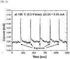
- FIGS. 1a to 1c illustrate changes in the sensitivity of a hydrogen sensor depending on the temperature.
- FIGS. 1a , 1b and 1c show changes in the sensitivity of a hydrogen sensor at different temperatures. With reference to FIGS. 1a , 1b and 1c , as the temperature is increased from room temperature to 100°C and 500°C, the sensitivity of the hydrogen sensor can be seen to increase.
- heat may be applied from the outside to decrease the reaction time of the sensing material and the detection target material.
- a gallium nitride-based sensor using a high-temperature epitaxy process makes it difficult to manufacture a heater for supplying heat to the sensing material.
- Conventional techniques are a process of growing no epitaxial thin film, in which, for instance, a gas sensor manufactured on a Si substrate is obtained by first forming a micro heater (Pt, etc.) on a membrane structure, forming a sensor structure thereon, and performing backside silicon etching.
- a micro heater Pt, etc.
- GaN-based sensor Since a GaN-based sensor is problematic in that an epitaxial thin film cannot be grown after the first formation of a heater (GaN-based epitaxy growth temperature is 1,000°C or more), a sensor structure is formed using an epitaxial thin film already grown at high temperatures and a heater structure is formed on the sensor structure. In this case, however, the distance from the heater region to the sensing material is long and thus a large amount of power is consumed in order to control the temperature and the sensor area has to include the heater region, undesirably enlarging the size of the sensor.
- GaN-based epitaxy growth temperature is 1,000°C or more
- the present invention has been made keeping in mind the above problems encountered in the related art, and the present invention is intended to provide a method of manufacturing a gallium nitride-based sensor having a heater structure.
- the present invention is intended to provide a gallium nitride-based sensor having a heater structure.
- the present invention provides a method of manufacturing a gallium nitride-based sensor having a heater structure, comprising growing an n-type or p-type GaN layer on a substrate, growing a GaN (Al x Ga 1-x N, In x Al 1-x N, or high-resistance GaN)-based monolayered or multilayered barrier layer on the n-type or p-type GaN layer, sequentially growing a u-GaN layer and a layer selected from the group consisting of an Al x Ga 1-x N layer, an In x Al 1-x N layer and an In x Al y Ga 1-x-y N layer on the barrier layer, patterning the n-type or p-type GaN layer so as to form an electrode, forming the electrode along the pattern formed on the n-type or p-type GaN layer, and forming a sensing material layer on the layer selected from the group consisting of the Al x Ga 1-x N layer, the In x Al 1-x N layer and the Indium
- the n-type or p-type GaN layer may function as a heater for generating heat due to the current applied to the electrode.
- the threshold voltage of the sensor device may be adjusted by changing the applied voltage.
- the barrier layer may be provided in the form of any one layer or a combination of layers selected from among an Al x Ga 1-x N layer, an In x Al 1-x N layer and a high-resistance GaN layer.
- the barrier layer may function to prevent the current flowing in the n-type or p-type GaN layer from flowing to the sensor structure on the barrier layer.
- the barrier layer may function to prevent the current flowing in the n-type or p-type GaN layer from flowing to the sensor structure on the barrier layer.
- the forming the sensing material layer on the layer selected from the group consisting of the Al x Ga 1-x N layer, the In x Al 1-x N layer and the In x Al y Ga 1-x-y N layer may include forming a source electrode and a drain electrode on the layer selected from the group consisting of the Al x Ga 1-x N layer, the In x Al 1-x N layer and the In x Al y Ga 1-x-y N layer, and forming the sensing material layer on a portion of the region between the source electrode and the drain electrode.
- a GaN cap layer, an oxide film layer or a nitride film layer may be further formed in a single layer or multiple layers on the layer selected from the group consisting of the Al x Ga 1-x N layer, the In x Al 1-x N layer and the In x Al y Ga 1-x-y N layer, and the thickness of the GaN cap layer, the oxide film layer or the nitride film layer may be 30 nm or less.
- the forming the sensing material layer on the layer selected from the group consisting of the Al x Ga 1-x N layer, the In x Al 1-x N layer and the In x Al y Ga 1-x-y N layer may include forming an ohmic contact electrode on the layer selected from the group consisting of the Al x Ga 1-x N layer, the In x Al 1-x N layer and the In x Al y Ga 1-x-y N layer, and forming the sensing material layer for Schottky contact formation and an ohmic contact electrode connected thereto.
- the heat generated by applying current to the n-type or p-type GaN layer may be transferred to the sensing material layer.
- x In the Al x Ga 1-x N layer, x may satisfy 0 ⁇ x ⁇ 1, and in the In x Al 1-x N layer, x may satisfy 0 ⁇ x ⁇ 1.
- x and y may satisfy 0 ⁇ x ⁇ 1, 0 ⁇ y ⁇ 1, 0 ⁇ (x+y) ⁇ 1.
- x In the Al x Ga 1-x N layer for forming the barrier layer, x may satisfy 0 ⁇ x ⁇ 1, and in the In x Al 1-x N layer for forming the barrier layer, x may satisfy 0 ⁇ x ⁇ 1.
- the method of the invention may further include separating the substrate from the n-type or p-type GaN layer.
- the substrate may be made of any one material selected from the group consisting of sapphire, AlN, diamond, BN, SiC, Si and GaN.
- the present invention provides a gallium nitride-based sensor having a heater structure, comprising a substrate, an n-type or p-type GaN layer grown on the substrate, a GaN (Al x Ga 1-x N, In x Al 1-x N, or high-resistance GaN) -based monolayered or multilayered barrier layer grown on the n-type or p-type GaN layer, a u-GaN layer grown on the barrier layer, a layer selected from the group consisting of an Al x Ga 1-x N layer, an In x Al 1-x N layer and an In x Al y Ga 1-x-y N layer grown on the u-GaN layer, an electrode formed along a pattern formed on the n-type or p-type GaN layer, and a sensing material layer formed on the layer selected from the group consisting of the Al x Ga 1-x N layer, the In x Al 1-x N layer and the In x Al y Ga 1-x-y N layer.
- the n-type or p-type GaN layer may function as a heater for generating heat due to the current applied to the electrode.
- the threshold voltage of the sensor device may be adjusted by changing the applied voltage.
- the barrier layer may be provided in the form of any one layer or a combination of layers selected from among an Al x Ga 1-x N layer, an In x Al 1-x N layer and a high-resistance GaN layer.
- the barrier layer may function to prevent the current flowing in the n-type or p-type GaN layer from flowing to the sensor structure on the barrier layer.
- the senor of the invention may further include a source electrode and a drain electrode formed on the layer selected from the group consisting of the Al x Ga 1-x N layer, the In x Al 1-x N layer and the In x Al y Ga 1-x-y N layer, and the sensing material layer may be formed on a portion of the region between the source electrode and the drain electrode.
- the senor of the invention may further include an ohmic contact electrode, formed on the layer selected from the group consisting of the Al x Ga 1-x N layer, the In x Al 1-x N layer and the In x Al y Ga 1-x-y N layer, and an ohmic contact electrode connected to the sensing material layer for Schottky contact formation.
- an ohmic contact electrode formed on the layer selected from the group consisting of the Al x Ga 1-x N layer, the In x Al 1-x N layer and the In x Al y Ga 1-x-y N layer, and an ohmic contact electrode connected to the sensing material layer for Schottky contact formation.
- x In the Al x Ga 1-x N layer, x may satisfy 0 ⁇ x ⁇ 1, and in the In x Al 1-x N layer, x may satisfy 0 ⁇ x ⁇ 1.
- x and y may satisfy 0 ⁇ x ⁇ 1, 0 ⁇ y ⁇ 1, 0 ⁇ (x+y) ⁇ 1.
- x In the Al x Ga 1-x N layer for forming the barrier layer, x may satisfy 0 ⁇ x ⁇ 1, and in the In x Al 1-x N layer for forming the barrier layer, x may satisfy 0 ⁇ x ⁇ 1.
- the heat generated by applying current to the n-type or p-type GaN layer may be transferred to the sensing material layer.
- the substrate may be made of any one material selected from the group consisting of sapphire, AlN, diamond, BN, SiC, Si and GaN.
- the n-type or p-type GaN layer formed on the substrate may be formed in a stripe shape, and the thickness, width, gap, and electrical conductivity of the stripe shape may be adjusted to thereby facilitate control of the reaction time (sensitivity) of the sensing material layer and the restoration time.
- the substrate may be separated from the n-type or p-type GaN layer and then transferred to a third substrate.
- the third substrate may be made of Si, Ge, W, Cr, Ni, Cu or alloys thereof, amorphous AlN, amorphous SiC, graphite, nanocarbon, or a polymer material.
- the polymer material may include any one selected from the group consisting of polycarbonate (PC), polyethylene naphthalate (PEN), polynorbornene, polyacrylate, polyvinyl alcohol, polyimide, polyethylene terephthalate (PET), polyethersulfone (PES), polystyrene (PS), polypropylene (PP), polyethylene (PE), polyvinylchloride (PVC), polyamide (PA), polybutylene terephthalate (PBT), polymethyl methacrylate (PMMA) and polydimethylsiloxane (PDMS).
- PC polycarbonate
- PEN polyethylene naphthalate
- PET polyethylene terephthalate
- PES polyethersulfone
- PS polystyrene
- PP polypropylene
- PE polyethylene
- PVC polyvinylchloride
- PA polyamide
- PBT polybutylene terephthalate
- PMMA polymethyl methacrylate
- PDMS polydimethyl
- a HEMT sensor or a Schottky diode sensor can be heated using an n-GaN (or p-GaN) layer, thus increasing the sensitivity of the sensor and decreasing the restoration time.
- the heater structure using the n-GaN (or p-GaN) layer is located directly below the sensor structure, thereby reducing power consumption and rapidly changing the temperature of the sensing material.
- an n-GaN (or p-GaN) epitaxial layer having high conductivity and a barrier layer usable as an insulator are grown on a heterogeneous substrate (sapphire, AlN, diamond, BN, Si, SiC, etc.), and then a HEMT structure, a Schottky diode structure, or the like is formed, thereby easily manufacturing the gallium nitride-based sensor having a heater structure.
- first, second, A, “B”, etc. may be used herein to describe various elements, these elements are not intended to be limited by these terms. These terms are only used to distinguish one element from another element. For instance, a first element discussed below could be termed a second element without departing from the teachings of the present invention. Similarly, the second element could also be termed the first element. As used herein, the term “and/or” may include any one of the listed items and any combination of one or more thereof.
- FIG. 2 illustrates the epitaxial thin film growth for manufacturing a gallium nitride-based sensor having a heater structure according to an embodiment of the present invention.
- the epitaxial thin film for manufacturing a gallium nitride-based sensor having a heater structure may be configured to include a substrate 10, an n-type or p-type GaN layer 20 grown on the substrate, a GaN (Al x Ga 1-x N, In x Al 1-x N, or high-resistance GaN) -based monolayered or multilayered barrier layer 30 grown on the n-type or p-type GaN layer, a u-GaN layer 40 grown on the barrier layer 30, and a layer 50 selected from the group consisting of an Al x Ga 1-x N layer, an In x Al 1-x N layer and an In x Al y Ga 1-x-y N layer, grown on the u-GaN layer.
- the substrate 10 may be made of any one material selected from the group consisting of sapphire, AlN, diamond, BN, SiC, Si and GaN.
- the n-type or p-type GaN layer 20 may function as a heater for generating heat due to the current applied to an electrode.
- the barrier layer 30 is formed on the n-type or p-type GaN layer 20, when current is applied to the n-type or p-type GaN layer 20, the current flows in the transverse direction of the n-type or p-type GaN layer 20, thereby generating heat.
- the barrier layer 30 may be provided in the form of any one layer or a combination of layers selected from among an Al x Ga 1-x N layer, an In x Al 1-x N layer and a high-resistance GaN layer, and may function to prevent the current flowing in the n-type or p-type GaN layer 20 from flowing to the sensor structure on the barrier layer 30.
- the n-type or p-type GaN layer 20 having high conductivity is interposed between the substrate 10 and the barrier layer 30, whereby epitaxial thin film growth may be performed.
- FIG. 3 illustrates the MESA isolation on the epitaxial thin film for manufacturing a gallium nitride-based sensor having a heater structure according to an embodiment of the present invention
- FIG. 4 illustrates the patterning for forming an electrode on the epitaxial thin film for manufacturing a gallium nitride-based sensor having a heater structure according to an embodiment of the present invention
- FIG. 5 illustrates the electrode formation and the HEMT formation for manufacturing a gallium nitride-based sensor having a heater structure according to an embodiment of the present invention.
- the epitaxial thin film as shown in FIG. 2 comprising the substrate 10, the n-type or p-type GaN layer 20, the barrier layer 30, the u-GaN layer 40 and the layer 50 selected from the group consisting of the Al x Ga 1-x N layer, the In x Al 1-x N layer and the In x Al y Ga 1-x-y N layer, may be grown, and such a thin film structure is made structurally stable by continuously growing the GaN-based layers.
- a GaN cap layer, an oxide film layer or a nitride film layer may be further formed in a single layer or multiple layers on the layer selected from the group consisting of the Al x Ga 1-x N layer, the In x Al 1-x N layer and the In x Al y Ga 1-x-y N layer.
- the GaN cap layer, the oxide film layer or the nitride film layer preferably has a thickness of 30 nm or less.
- the thickness of the GaN cap layer, the oxide film layer or the nitride film layer may be 10 nm ⁇ 30 nm.
- the MESA isolation may be performed on the thin film structure of FIG. 2 for manufacturing the gallium nitride-based sensor having a heater structure. Specifically, some outer portions of the layer 50 selected from the group consisting of the Al x Ga 1-x N layer, the In x Al 1-x N layer and the In x Al y Ga 1-x-y N layer, the u-GaN layer 40, and the barrier layer 30 may be etched.
- the patterning for forming an electrode may be performed on the epitaxial thin film for manufacturing the gallium nitride-based sensor having a heater structure. Specifically, the n-type or p-type GaN layer 20 may be patterned so as to contact the electrode.
- the electrode 60 may be formed along the pattern formed on the n-type or p-type GaN layer 20.
- a source electrode S and a drain electrode D may be formed on the layer 50 selected from the group consisting of the Al x Ga 1-x N layer, the In x Al 1-x N layer and the In x Al y Ga 1-x-y N layer, and a sensing material layer SM may be formed on a portion of the region between the source electrode S and the drain electrode D, thereby manufacturing a gallium nitride-based HEMT sensor.
- the sensing material layer may be formed in a recess region PI made by etching a portion of the layer 50 selected from the group consisting of the Al x Ga 1-x N layer, the In x Al 1-x N layer and the In x Al y Ga 1-x-y N layer.
- the value x of the Al x Ga 1-x N layer may satisfy 0 ⁇ x ⁇ 1
- the value x of the In x Al 1-x N layer may satisfy 0 ⁇ x ⁇ 1
- the values x and y of the In x Al y Ga 1-x-y N layer may satisfy 0 ⁇ x ⁇ 1, 0 ⁇ y ⁇ 1, 0 ⁇ (x+y) ⁇ 1.
- the value x of the Al x Ga 1-x N layer for forming the barrier layer 30 may satisfy 0 ⁇ x ⁇ 1, and the value x of the In x Al 1-x N layer for forming the barrier layer 30 may satisfy 0 ⁇ x ⁇ 1.
- the n-type or p-type GaN layer 20 may function as a heater for generating heat due to current applied to the electrode 60.
- the gallium nitride-based HEMT sensor may be configured such that heat generated by applying current to the n-type or p-type GaN layer 20 may be rapidly transferred to the sensing material layer SM via the barrier layer, the u-GaN layer and the layer selected from the group consisting of the Al x Ga 1-x N layer, the In x Al 1-x N layer and the In x Al y Ga 1-x-y N layer.
- FIG. 6 illustrates the electrode formation and the Schottky diode formation for manufacturing the gallium nitride-based sensor having a heater structure according to an embodiment of the present invention.
- the epitaxial thin film as shown in FIG. 2 comprising the substrate 10, the n-type or p-type GaN layer 20, the barrier layer 30, the u-GaN layer 40 and the layer 50 selected from the group consisting of the Al x Ga 1-x N layer, the In x Al 1-x N layer and the In x Al y Ga 1-x-y N layer, may be grown, and such a thin film structure is made structurally stable by continuously growing the GaN-based layers.
- the MESA isolation may be performed on the thin film structure of FIG. 2 for manufacturing the gallium nitride-based sensor having a heater structure. Specifically, some outer portions of the layer 50 selected from the group consisting of the Al x Ga 1-x N layer, the In x Al 1-x N layer and the In x Al y Ga 1-x-y N layer, the u-GaN layer 40, and the barrier layer 30 may be etched.
- the patterning for forming an electrode may be performed on the epitaxial thin film for manufacturing the gallium nitride-based sensor having a heater structure. Specifically, the n-type or p-type GaN layer 20 may be patterned so as to contact the electrode.
- the electrode 60 may be formed along the pattern formed on the n-type or p-type GaN layer 20.
- an ohmic contact electrode 71 may be formed on the layer 50 selected from the group consisting of the Al x Ga 1-x N layer, the In x Al 1-x N layer and the In x Al y Ga 1-x-y N layer, and an ohmic contact electrode 72 that is connected to a sensing material layer (SBSM: Schottky Barrier Sensing Materials) for Schottky contact formation may be formed, thereby manufacturing a gallium nitride-based Schottky diode sensor.
- SBSM Schottky Barrier Sensing Materials
- the n-type or p-type GaN layer 20 may function as a heater for generating heat due to current applied to the electrode 60.
- the gallium nitride-based Schottky diode sensor may be configured such that heat generated by applying current to the n-type or p-type GaN layer 20 may be rapidly transferred to the sensing material layer (SBSM) via the barrier layer, the u-GaN layer and the layer selected from the group consisting of the Al x Ga 1-x N layer, the In x Al 1-x N layer and the In x Al y Ga 1-x-y N layer.
- SBSM sensing material layer
- FIG. 7 illustrates the electrode formation and the membrane formation for manufacturing the gallium nitride-based sensor having a heater structure according to an embodiment of the present invention.
- the epitaxial thin film as shown in FIG. 2 comprising the substrate 10, the n-type or p-type GaN layer 20, the barrier layer 30, the u-GaN layer 40 and the layer 50 selected from the group consisting of the Al x Ga 1-x N layer, the In x Al 1-x N layer and the In x Al y Ga 1-x-y N layer, may be grown, and such a thin film structure is made structurally stable by continuously growing the GaN-based layers.
- the MESA isolation may be performed on the thin film structure of FIG. 2 for manufacturing the gallium nitride-based sensor having a heater structure. Specifically, some outer portions of the layer 50 selected from the group consisting of the Al x Ga 1-x N layer, the In x Al 1-x N layer and the In x Al y Ga 1-x-y N layer, the u-GaN layer 40, and the barrier layer 30 may be etched.
- the patterning for forming an electrode may be carried out on the epitaxial thin film for manufacturing the gallium nitride-based sensor having a heater structure. Specifically, the n-type or p-type GaN layer 20 may be patterned so as to contact the electrode.
- the electrode 60 may be formed along the pattern formed on the n-type or p-type GaN layer 20.
- a source electrode S and a drain electrode D may be formed on the layer 50 selected from the group consisting of the Al x Ga 1-x N layer, the In x Al 1-x N layer and the In x Al y Ga 1-x-y N layer, a sensing material layer SM may be formed on a portion of the region between the source electrode S and the drain electrode D, and the substrate 10 may be separated from the n-type or p-type GaN layer 20 and then transferred to a third substrate, thereby manufacturing a gallium nitride-based membrane or flexible sensor.
- the sensing material layer may be formed in a recess region P1 made by etching a portion of the layer 50 selected from the group consisting of the Al x Ga 1-x N layer, the In x Al 1-x N layer and the In x Al y Ga 1-x-y N layer.
- FIG. 8 illustrates the manufacture of a gallium nitride-based sensor having a heater structure according to another embodiment of the present invention.
- an insulator layer 80 may be formed in a stripe shape on a substrate 10.
- An n-type or p-type GaN layer 20 may be grown on the substrate 10 having the stripe-shaped insulator layer 80 formed thereon, and such an n-type or p-type GaN layer 20 may function as a heater. Specifically, the n-type or p-type GaN layer 20 may be grown in the stripe-shaped insulator layer 80 to thus have a stripe shape.
- a sensor structure may be formed on the insulator layer 80 and the n-type or p-type GaN layer 20, having the stripe shape, thereby manufacturing a gallium nitride-based sensor having a heater structure.
- the stripe-shaped n-type or p-type GaN layer 20 is adjusted in the thickness, width, gap, and electrical conductivity of the stripe shape, thus obtaining the gallium nitride-based sensor in which the temperature of the sensing material layer, power consumption, etc. may be easily controlled.
- a GaN-based buffer layer may be interposed between the insulator layer 80 and the substrate.
- the heater layer 20 may be patterned so as to have a planar structure or a one-dimensional linear structure.
- the substrate is separated from the n-type or p-type GaN layer 20, and may be transferred to the third substrate, and the third substrate may be made of Si, Ge, W, Cr, Ni, Cu or alloys thereof, amorphous AlN, amorphous SiC, graphite, nanocarbon, or a polymer material.
- the polymer material may include any one selected from the group consisting of polycarbonate (PC), polyethylene naphthalate (PEN), polynorbornene, polyacrylate, polyvinyl alcohol, polyimide, polyethylene terephthalate (PET), polyethersulfone (PES), polystyrene (PS), polypropylene (PP), polyethylene (PE), polyvinylchloride (PVC), polyamide (PA), polybutylene terephthalate (PBT), polymethyl methacrylate (PMMA) and polydimethylsiloxane (PDMS).
- PC polycarbonate
- PEN polyethylene naphthalate
- PET polyethylene terephthalate
- PES polyethersulfone
- PS polystyrene
- PP polypropylene
- PE polyethylene
- PVC polyvinylchloride
- PA polyamide
- PBT polybutylene terephthalate
- PMMA polymethyl methacrylate
- PDMS polydimethyl
- the gallium nitride-based sensor having a heater structure may be configured such that a process of growing an epitaxial thin film having high conductivity is included during the gallium nitride-based epitaxial thin film growth, and thus a heater structure may be embedded.
- an n-GaN (or p-GaN) epitaxial layer having high conductivity and a barrier layer usable as an insulator are grown, and then a HEMT structure, a Schottky diode structure, or the like is formed, thereby manufacturing the gallium nitride-based sensor having a heater structure.
Landscapes
- Chemical & Material Sciences (AREA)
- Health & Medical Sciences (AREA)
- Life Sciences & Earth Sciences (AREA)
- Immunology (AREA)
- Physics & Mathematics (AREA)
- Analytical Chemistry (AREA)
- Biochemistry (AREA)
- General Health & Medical Sciences (AREA)
- General Physics & Mathematics (AREA)
- Pathology (AREA)
- Electrochemistry (AREA)
- Chemical Kinetics & Catalysis (AREA)
- Engineering & Computer Science (AREA)
- Microelectronics & Electronic Packaging (AREA)
- Molecular Biology (AREA)
- Combustion & Propulsion (AREA)
- Food Science & Technology (AREA)
- Medicinal Chemistry (AREA)
- Power Engineering (AREA)
- Junction Field-Effect Transistors (AREA)
- Investigating Or Analyzing Materials By The Use Of Electric Means (AREA)
Description
- The present invention relates to the manufacture of a gallium nitride-based sensor, and more particularly to a gallium nitride-based sensor having a heater structure and a method of manufacturing the same.
- Gallium nitride (GaN) has a high energy bandgap of 3.4 eV and an intrinsic carrier concentration of 10-10 cm-3 at room temperature and thus retains high durability and enables the stable operation of devices even under conditions of high temperatures of 600°C or more, high pressure and electromagnetic waves, compared to silicon and oxide semiconductors.
- Also, GaN, having large lattice energy and a chemically stable structure, may exhibit outstanding chemical stability under conditions of strong acids and bases and high humidity compared to oxide semiconductors in the form of a thin film or a nanostructure.
- In particular, an AlGaN/GaN HEMT (High Electron Mobility Transistor), configured such that an AlGaN thin film is grown on GaN, is able to form a 2-DEG (2-Dimensional Electron Gas) layer having very fast electron mobility at the interface of AlGaN and GaN through spontaneous polarization and piezoelectric effects due to mismatch of lattice constants, in which the 2-DEG layer exhibits a current change that is very sensitive to changes in charge quantity on a semiconductor surface, making it possible to manufacture a stable sensor, having a very small size, low power, fast response speed, and high sensitivity, using the same.
-
FIGS. 1a to 1c illustrate changes in the sensitivity of a hydrogen sensor depending on the temperature. -
FIGS. 1a ,1b and1c show changes in the sensitivity of a hydrogen sensor at different temperatures. With reference toFIGS. 1a ,1b and1c , as the temperature is increased from room temperature to 100°C and 500°C, the sensitivity of the hydrogen sensor can be seen to increase. - Specifically, in the case of a gas sensor or a chemical sensor, which is reusable using a sensing material, it is very important to reduce the reaction time required to detect a detection target material using a sensing material and the restoration time required to restore the sensor to the original state thereof after removal of the detection target material.
- With the goal of reducing the reaction time (sensitivity) and the restoration time, heat may be applied from the outside to decrease the reaction time of the sensing material and the detection target material.
- However, a gallium nitride-based sensor using a high-temperature epitaxy process makes it difficult to manufacture a heater for supplying heat to the sensing material.
- Conventional techniques are a process of growing no epitaxial thin film, in which, for instance, a gas sensor manufactured on a Si substrate is obtained by first forming a micro heater (Pt, etc.) on a membrane structure, forming a sensor structure thereon, and performing backside silicon etching.
- Since a GaN-based sensor is problematic in that an epitaxial thin film cannot be grown after the first formation of a heater (GaN-based epitaxy growth temperature is 1,000°C or more), a sensor structure is formed using an epitaxial thin film already grown at high temperatures and a heater structure is formed on the sensor structure. In this case, however, the distance from the heater region to the sensing material is long and thus a large amount of power is consumed in order to control the temperature and the sensor area has to include the heater region, undesirably enlarging the size of the sensor.
- Although the manufacture of a physical sensor, a chemical sensor, a biosensor, etc. using a GaN-based thin film requires the temperature of the sensor device to be controlled, it is difficult to manufacture a heater having low power consumption owing to the high heat capacity of the substrate having the GaN-based thin film grown thereon.
- Moreover, it is not easy to perform a process of removing a portion of the substrate having the GaN-based thin film grown thereon in order to reduce the heat capacity of the region for manufacturing the sensor, making it difficult to manufacture a gallium nitride-based sensor having a heater.
- The article "Finite element thermal analysis of localized heating in AlGaN/GaN HEMT based sensors" from Minmin Hou et al., the patent application
DE10032062 , and the article "Pt-AlGaN/GaN HEMT-Sensor for Hydrogen Sulfide (H2S) Detection" from Robert Sokolovskij et al., all disclose gallium nitride based sensors. - Accordingly, the present invention has been made keeping in mind the above problems encountered in the related art, and the present invention is intended to provide a method of manufacturing a gallium nitride-based sensor having a heater structure.
- In addition, the present invention is intended to provide a gallium nitride-based sensor having a heater structure.
- Therefore, the present invention provides a method of manufacturing a gallium nitride-based sensor having a heater structure, comprising growing an n-type or p-type GaN layer on a substrate, growing a GaN (AlxGa1-xN, InxAl1-xN, or high-resistance GaN)-based monolayered or multilayered barrier layer on the n-type or p-type GaN layer, sequentially growing a u-GaN layer and a layer selected from the group consisting of an AlxGa1-xN layer, an InxAl1-xN layer and an InxAlyGa1-x-yN layer on the barrier layer, patterning the n-type or p-type GaN layer so as to form an electrode, forming the electrode along the pattern formed on the n-type or p-type GaN layer, and forming a sensing material layer on the layer selected from the group consisting of the AlxGa1-xN layer, the InxAl1-xN layer and the InxAlyGa1-x-yN layer.
- Here, the n-type or p-type GaN layer may function as a heater for generating heat due to the current applied to the electrode. Also, the threshold voltage of the sensor device may be adjusted by changing the applied voltage.
- Here, the barrier layer may be provided in the form of any one layer or a combination of layers selected from among an AlxGa1-xN layer, an InxAl1-xN layer and a high-resistance GaN layer.
- Here, the barrier layer may function to prevent the current flowing in the n-type or p-type GaN layer from flowing to the sensor structure on the barrier layer.
- Here, the barrier layer may function to prevent the current flowing in the n-type or p-type GaN layer from flowing to the sensor structure on the barrier layer.
- Here, the forming the sensing material layer on the layer selected from the group consisting of the AlxGa1-xN layer, the InxAl1-xN layer and the InxAlyGa1-x-yN layer may include forming a source electrode and a drain electrode on the layer selected from the group consisting of the AlxGa1-xN layer, the InxAl1-xN layer and the InxAlyGa1-x-yN layer, and forming the sensing material layer on a portion of the region between the source electrode and the drain electrode.
- Here, a GaN cap layer, an oxide film layer or a nitride film layer may be further formed in a single layer or multiple layers on the layer selected from the group consisting of the AlxGa1-xN layer, the InxAl1-xN layer and the InxAlyGa1-x-yN layer, and the thickness of the GaN cap layer, the oxide film layer or the nitride film layer may be 30 nm or less.
- Here, the forming the sensing material layer on the layer selected from the group consisting of the AlxGa1-xN layer, the InxAl1-xN layer and the InxAlyGa1-x-yN layer may include forming an ohmic contact electrode on the layer selected from the group consisting of the AlxGa1-xN layer, the InxAl1-xN layer and the InxAlyGa1-x-yN layer, and forming the sensing material layer for Schottky contact formation and an ohmic contact electrode connected thereto.
- Here, the heat generated by applying current to the n-type or p-type GaN layer may be transferred to the sensing material layer.
- In the AlxGa1-xN layer, x may satisfy 0<x≤1, and in the InxAl1-xN layer, x may satisfy 0<x≤1.
- In the InxAlyGa1-x-yN layer, x and y may satisfy 0<x≤1, 0<y≤1, 0< (x+y) ≤1.
- In the AlxGa1-xN layer for forming the barrier layer, x may satisfy 0<x≤1, and in the InxAl1-xN layer for forming the barrier layer, x may satisfy 0<x≤1.
- The method of the invention may further include separating the substrate from the n-type or p-type GaN layer.
- Here, the substrate may be made of any one material selected from the group consisting of sapphire, AlN, diamond, BN, SiC, Si and GaN.
- In addition, the present invention provides a gallium nitride-based sensor having a heater structure, comprising a substrate, an n-type or p-type GaN layer grown on the substrate, a GaN (AlxGa1-xN, InxAl1-xN, or high-resistance GaN) -based monolayered or multilayered barrier layer grown on the n-type or p-type GaN layer, a u-GaN layer grown on the barrier layer, a layer selected from the group consisting of an AlxGa1-xN layer, an InxAl1-xN layer and an InxAlyGa1-x-yN layer grown on the u-GaN layer, an electrode formed along a pattern formed on the n-type or p-type GaN layer, and a sensing material layer formed on the layer selected from the group consisting of the AlxGa1-xN layer, the InxAl1-xN layer and the InxAlyGa1-x-yN layer.
- Here, the n-type or p-type GaN layer may function as a heater for generating heat due to the current applied to the electrode. Also, the threshold voltage of the sensor device may be adjusted by changing the applied voltage.
- Here, the barrier layer may be provided in the form of any one layer or a combination of layers selected from among an AlxGa1-xN layer, an InxAl1-xN layer and a high-resistance GaN layer.
- Here, the barrier layer may function to prevent the current flowing in the n-type or p-type GaN layer from flowing to the sensor structure on the barrier layer.
- Here, the sensor of the invention may further include a source electrode and a drain electrode formed on the layer selected from the group consisting of the AlxGa1-xN layer, the InxAl1-xN layer and the InxAlyGa1-x-yN layer, and the sensing material layer may be formed on a portion of the region between the source electrode and the drain electrode.
- Here, the sensor of the invention may further include an ohmic contact electrode, formed on the layer selected from the group consisting of the AlxGa1-xN layer, the InxAl1-xN layer and the InxAlyGa1-x-yN layer, and an ohmic contact electrode connected to the sensing material layer for Schottky contact formation.
- In the AlxGa1-xN layer, x may satisfy 0<x≤1, and in the InxAl1-xN layer, x may satisfy 0<x≤1.
- In the InxAlyGa1-x-yN layer, x and y may satisfy 0<x≤1, 0<y≤1, 0<(x+y)≤1.
- In the AlxGa1-xN layer for forming the barrier layer, x may satisfy 0<x≤1, and in the InxAl1-xN layer for forming the barrier layer, x may satisfy 0<x≤1.
- Here, the heat generated by applying current to the n-type or p-type GaN layer may be transferred to the sensing material layer.
- Here, the substrate may be made of any one material selected from the group consisting of sapphire, AlN, diamond, BN, SiC, Si and GaN.
- Here, the n-type or p-type GaN layer formed on the substrate may be formed in a stripe shape, and the thickness, width, gap, and electrical conductivity of the stripe shape may be adjusted to thereby facilitate control of the reaction time (sensitivity) of the sensing material layer and the restoration time.
- Here, the substrate may be separated from the n-type or p-type GaN layer and then transferred to a third substrate.
- Here, the third substrate may be made of Si, Ge, W, Cr, Ni, Cu or alloys thereof, amorphous AlN, amorphous SiC, graphite, nanocarbon, or a polymer material.
- Here, the polymer material may include any one selected from the group consisting of polycarbonate (PC), polyethylene naphthalate (PEN), polynorbornene, polyacrylate, polyvinyl alcohol, polyimide, polyethylene terephthalate (PET), polyethersulfone (PES), polystyrene (PS), polypropylene (PP), polyethylene (PE), polyvinylchloride (PVC), polyamide (PA), polybutylene terephthalate (PBT), polymethyl methacrylate (PMMA) and polydimethylsiloxane (PDMS).
- According to the present invention pertaining to a gallium nitride-based sensor having a heater structure and a method of manufacturing the same, a HEMT sensor or a Schottky diode sensor can be heated using an n-GaN (or p-GaN) layer, thus increasing the sensitivity of the sensor and decreasing the restoration time. As such, the heater structure using the n-GaN (or p-GaN) layer is located directly below the sensor structure, thereby reducing power consumption and rapidly changing the temperature of the sensing material.
- Also, an n-GaN (or p-GaN) epitaxial layer having high conductivity and a barrier layer usable as an insulator are grown on a heterogeneous substrate (sapphire, AlN, diamond, BN, Si, SiC, etc.), and then a HEMT structure, a Schottky diode structure, or the like is formed, thereby easily manufacturing the gallium nitride-based sensor having a heater structure.
-
-
FIGS. 1a to 1c illustrate changes in sensitivity of a hydrogen sensor depending on the temperature; -
FIG. 2 illustrates the epitaxial thin film growth for manufacturing a gallium nitride-based sensor having a heater structure according to an embodiment of the present invention; -
FIG. 3 illustrates the MESA isolation on the epitaxial thin film for manufacturing a gallium nitride-based sensor having a heater structure according to an embodiment of the present invention; -
FIG. 4 illustrates the patterning for forming an electrode on the epitaxial thin film for manufacturing a gallium nitride-based sensor having a heater structure according to an embodiment of the present invention; -
FIG. 5 illustrates the electrode formation and the HEMT formation for manufacturing a gallium nitride-based sensor having a heater structure according to an embodiment of the present invention; -
FIG. 6 illustrates the electrode formation and the Schottky diode formation for manufacturing a gallium nitride-based sensor having a heater structure according to an embodiment of the present invention; -
FIG. 7 illustrates the electrode formation and the membrane formation for manufacturing a gallium nitride-based sensor having a heater structure according to an embodiment of the present invention; and -
FIG. 8 illustrates the manufacture of a gallium nitride-based sensor having a heater structure according to another embodiment of the present invention. - Reference will now be made in detail to various embodiments of the present invention, specific examples of which are illustrated in the accompanying drawings and described below, since the embodiments of the present invention can be variously modified in many different forms. While the present invention will be described in conjunction with exemplary embodiments thereof, it is to be understood that the present description is not intended to limit the present invention to those exemplary embodiments. On the contrary, the present invention is intended to cover not only the exemplary embodiments, but also various alternatives, modifications, equivalents and other embodiments that may be included within the spirit and scope of the present invention as defined by the appended claims. Throughout the drawings, the same reference numerals refer to the same or like elements.
- It will be understood that, although the terms "first", "second", "A", "B", etc. may be used herein to describe various elements, these elements are not intended to be limited by these terms. These terms are only used to distinguish one element from another element. For instance, a first element discussed below could be termed a second element without departing from the teachings of the present invention. Similarly, the second element could also be termed the first element. As used herein, the term "and/or" may include any one of the listed items and any combination of one or more thereof.
- It will be understood that when an element is referred to as being "coupled" or "connected" to another element, it can be directly coupled or connected to the other element, or intervening elements may be present therebetween. In contrast, it should be understood that when an element is referred to as being "directly coupled" or "directly connected" to another element, there are no intervening elements present.
- The terminology used herein is for the purpose of describing particular embodiments only and is not intended to be limiting of the present invention. As used herein, the singular forms are intended to include the plural forms as well, unless the context clearly indicates otherwise. It will be further understood that the terms "comprises", "comprising", "includes" and/or "including", when used herein, specify the presence of stated features, integers, steps, operations, elements, and/or components, but do not preclude the presence or addition of one or more other features, integers, steps, operations, elements, components, and/or groups thereof.
- Unless otherwise defined, all terms including technical and scientific terms used herein have the same meaning as commonly understood by one of ordinary skill in the art to which the present invention belongs. It will be further understood that terms used herein should be interpreted as having a meaning that is consistent with their meaning in the context of this specification and the relevant art and are not to be interpreted in an idealized or overly formal sense unless expressly so defined herein.
- Hereinafter, a detailed description will be given of preferred embodiments of the present invention with reference to the appended drawings.
-
FIG. 2 illustrates the epitaxial thin film growth for manufacturing a gallium nitride-based sensor having a heater structure according to an embodiment of the present invention. - With reference to
FIG. 2 , the epitaxial thin film for manufacturing a gallium nitride-based sensor having a heater structure according to an embodiment of the present invention may be configured to include asubstrate 10, an n-type or p-type GaN layer 20 grown on the substrate, a GaN (AlxGa1-xN, InxAl1-xN, or high-resistance GaN) -based monolayered ormultilayered barrier layer 30 grown on the n-type or p-type GaN layer, au-GaN layer 40 grown on thebarrier layer 30, and alayer 50 selected from the group consisting of an AlxGa1-xN layer, an InxAl1-xN layer and an InxAlyGa1-x-yN layer, grown on the u-GaN layer. Herein, thesubstrate 10 may be made of any one material selected from the group consisting of sapphire, AlN, diamond, BN, SiC, Si and GaN. - In particular, the n-type or p-
type GaN layer 20 may function as a heater for generating heat due to the current applied to an electrode. Specifically, since thebarrier layer 30 is formed on the n-type or p-type GaN layer 20, when current is applied to the n-type or p-type GaN layer 20, the current flows in the transverse direction of the n-type or p-type GaN layer 20, thereby generating heat. Here, thebarrier layer 30 may be provided in the form of any one layer or a combination of layers selected from among an AlxGa1-xN layer, an InxAl1-xN layer and a high-resistance GaN layer, and may function to prevent the current flowing in the n-type or p-type GaN layer 20 from flowing to the sensor structure on thebarrier layer 30. - The n-type or p-
type GaN layer 20 having high conductivity is interposed between thesubstrate 10 and thebarrier layer 30, whereby epitaxial thin film growth may be performed. -
FIG. 3 illustrates the MESA isolation on the epitaxial thin film for manufacturing a gallium nitride-based sensor having a heater structure according to an embodiment of the present invention,FIG. 4 illustrates the patterning for forming an electrode on the epitaxial thin film for manufacturing a gallium nitride-based sensor having a heater structure according to an embodiment of the present invention, andFIG. 5 illustrates the electrode formation and the HEMT formation for manufacturing a gallium nitride-based sensor having a heater structure according to an embodiment of the present invention. - With reference to
FIGS. 2 to 5 , the manufacture of a gallium nitride-based HEMT sensor having a heater structure is described below. - The epitaxial thin film as shown in
FIG. 2 , comprising thesubstrate 10, the n-type or p-type GaN layer 20, thebarrier layer 30, theu-GaN layer 40 and thelayer 50 selected from the group consisting of the AlxGa1-xN layer, the InxAl1-xN layer and the InxAlyGa1-x-yN layer, may be grown, and such a thin film structure is made structurally stable by continuously growing the GaN-based layers. - As necessary, a GaN cap layer, an oxide film layer or a nitride film layer may be further formed in a single layer or multiple layers on the layer selected from the group consisting of the AlxGa1-xN layer, the InxAl1-xN layer and the InxAlyGa1-x-yN layer. The GaN cap layer, the oxide film layer or the nitride film layer preferably has a thickness of 30 nm or less. For example, the thickness of the GaN cap layer, the oxide film layer or the nitride film layer may be 10 nm ∼ 30 nm.
- With reference to
FIG. 3 , the MESA isolation may be performed on the thin film structure ofFIG. 2 for manufacturing the gallium nitride-based sensor having a heater structure. Specifically, some outer portions of thelayer 50 selected from the group consisting of the AlxGa1-xN layer, the InxAl1-xN layer and the InxAlyGa1-x-yN layer, theu-GaN layer 40, and thebarrier layer 30 may be etched. - With reference to
FIG. 4 , the patterning for forming an electrode may be performed on the epitaxial thin film for manufacturing the gallium nitride-based sensor having a heater structure. Specifically, the n-type or p-type GaN layer 20 may be patterned so as to contact the electrode. - With reference to
FIG. 5 , theelectrode 60 may be formed along the pattern formed on the n-type or p-type GaN layer 20. - Also, a source electrode S and a drain electrode D may be formed on the
layer 50 selected from the group consisting of the AlxGa1-xN layer, the InxAl1-xN layer and the InxAlyGa1-x-yN layer, and a sensing material layer SM may be formed on a portion of the region between the source electrode S and the drain electrode D, thereby manufacturing a gallium nitride-based HEMT sensor. Here, the sensing material layer may be formed in a recess region PI made by etching a portion of thelayer 50 selected from the group consisting of the AlxGa1-xN layer, the InxAl1-xN layer and the InxAlyGa1-x-yN layer. - For example, the value x of the AlxGa1-xN layer may satisfy 0<x≤1, the value x of the InxAl1-xN layer may satisfy 0<x≤1, and the values x and y of the InxAlyGa1-x-yN layer may satisfy 0<x≤1, 0<y≤1, 0<(x+y)≤1.
- The value x of the AlxGa1-xN layer for forming the
barrier layer 30 may satisfy 0<x≤1, and the value x of the InxAl1-xN layer for forming thebarrier layer 30 may satisfy 0<x≤1. - The n-type or p-
type GaN layer 20 may function as a heater for generating heat due to current applied to theelectrode 60. Thus, the gallium nitride-based HEMT sensor may be configured such that heat generated by applying current to the n-type or p-type GaN layer 20 may be rapidly transferred to the sensing material layer SM via the barrier layer, the u-GaN layer and the layer selected from the group consisting of the AlxGa1-xN layer, the InxAl1-xN layer and the InxAlyGa1-x-yN layer. -
FIG. 6 illustrates the electrode formation and the Schottky diode formation for manufacturing the gallium nitride-based sensor having a heater structure according to an embodiment of the present invention. - With reference to
FIGS. 2 to 4 andFIG. 6 , the manufacture of a gallium nitride-based Schottky diode sensor having a heater structure is described below. - The epitaxial thin film as shown in
FIG. 2 , comprising thesubstrate 10, the n-type or p-type GaN layer 20, thebarrier layer 30, theu-GaN layer 40 and thelayer 50 selected from the group consisting of the AlxGa1-xN layer, the InxAl1-xN layer and the InxAlyGa1-x-yN layer, may be grown, and such a thin film structure is made structurally stable by continuously growing the GaN-based layers. - With reference to
FIG. 3 , the MESA isolation may be performed on the thin film structure ofFIG. 2 for manufacturing the gallium nitride-based sensor having a heater structure. Specifically, some outer portions of thelayer 50 selected from the group consisting of the AlxGa1-xN layer, the InxAl1-xN layer and the InxAlyGa1-x-yN layer, theu-GaN layer 40, and thebarrier layer 30 may be etched. - With reference to
FIG. 4 , the patterning for forming an electrode may be performed on the epitaxial thin film for manufacturing the gallium nitride-based sensor having a heater structure. Specifically, the n-type or p-type GaN layer 20 may be patterned so as to contact the electrode. - With reference to
FIG. 6 , theelectrode 60 may be formed along the pattern formed on the n-type or p-type GaN layer 20. - Also, an
ohmic contact electrode 71 may be formed on thelayer 50 selected from the group consisting of the AlxGa1-xN layer, the InxAl1-xN layer and the InxAlyGa1-x-yN layer, and anohmic contact electrode 72 that is connected to a sensing material layer (SBSM: Schottky Barrier Sensing Materials) for Schottky contact formation may be formed, thereby manufacturing a gallium nitride-based Schottky diode sensor. - The n-type or p-
type GaN layer 20 may function as a heater for generating heat due to current applied to theelectrode 60. Thus, the gallium nitride-based Schottky diode sensor may be configured such that heat generated by applying current to the n-type or p-type GaN layer 20 may be rapidly transferred to the sensing material layer (SBSM) via the barrier layer, the u-GaN layer and the layer selected from the group consisting of the AlxGa1-xN layer, the InxAl1-xN layer and the InxAlyGa1-x-yN layer. -
FIG. 7 illustrates the electrode formation and the membrane formation for manufacturing the gallium nitride-based sensor having a heater structure according to an embodiment of the present invention. - With reference to
FIGS. 2 to 4 andFIG. 7 , the manufacture of a gallium nitride-based membrane sensor having a heater structure is described below. - The epitaxial thin film as shown in
FIG. 2 , comprising thesubstrate 10, the n-type or p-type GaN layer 20, thebarrier layer 30, theu-GaN layer 40 and thelayer 50 selected from the group consisting of the AlxGa1-xN layer, the InxAl1-xN layer and the InxAlyGa1-x-yN layer, may be grown, and such a thin film structure is made structurally stable by continuously growing the GaN-based layers. - With reference to
FIG. 3 , the MESA isolation may be performed on the thin film structure ofFIG. 2 for manufacturing the gallium nitride-based sensor having a heater structure. Specifically, some outer portions of thelayer 50 selected from the group consisting of the AlxGa1-xN layer, the InxAl1-xN layer and the InxAlyGa1-x-yN layer, theu-GaN layer 40, and thebarrier layer 30 may be etched. - With reference to
FIG. 4 , the patterning for forming an electrode may be carried out on the epitaxial thin film for manufacturing the gallium nitride-based sensor having a heater structure. Specifically, the n-type or p-type GaN layer 20 may be patterned so as to contact the electrode. - With reference to
FIG. 7 , theelectrode 60 may be formed along the pattern formed on the n-type or p-type GaN layer 20. - Also, a source electrode S and a drain electrode D may be formed on the
layer 50 selected from the group consisting of the AlxGa1-xN layer, the InxAl1-xN layer and the InxAlyGa1-x-yN layer, a sensing material layer SM may be formed on a portion of the region between the source electrode S and the drain electrode D, and thesubstrate 10 may be separated from the n-type or p-type GaN layer 20 and then transferred to a third substrate, thereby manufacturing a gallium nitride-based membrane or flexible sensor. Here, the sensing material layer may be formed in a recess region P1 made by etching a portion of thelayer 50 selected from the group consisting of the AlxGa1-xN layer, the InxAl1-xN layer and the InxAlyGa1-x-yN layer. -
FIG. 8 illustrates the manufacture of a gallium nitride-based sensor having a heater structure according to another embodiment of the present invention. - With reference to
FIG. 8 , aninsulator layer 80 may be formed in a stripe shape on asubstrate 10. - An n-type or p-
type GaN layer 20 may be grown on thesubstrate 10 having the stripe-shapedinsulator layer 80 formed thereon, and such an n-type or p-type GaN layer 20 may function as a heater. Specifically, the n-type or p-type GaN layer 20 may be grown in the stripe-shapedinsulator layer 80 to thus have a stripe shape. - Accordingly, a sensor structure may be formed on the
insulator layer 80 and the n-type or p-type GaN layer 20, having the stripe shape, thereby manufacturing a gallium nitride-based sensor having a heater structure. - The stripe-shaped n-type or p-
type GaN layer 20 is adjusted in the thickness, width, gap, and electrical conductivity of the stripe shape, thus obtaining the gallium nitride-based sensor in which the temperature of the sensing material layer, power consumption, etc. may be easily controlled. - In order to easily separate the substrate upon the formation of the stripe-shaped
insulator layer 80, a GaN-based buffer layer may be interposed between theinsulator layer 80 and the substrate. - For example, the
heater layer 20 may be patterned so as to have a planar structure or a one-dimensional linear structure. - Furthermore, the substrate is separated from the n-type or p-
type GaN layer 20, and may be transferred to the third substrate, and the third substrate may be made of Si, Ge, W, Cr, Ni, Cu or alloys thereof, amorphous AlN, amorphous SiC, graphite, nanocarbon, or a polymer material. - The polymer material may include any one selected from the group consisting of polycarbonate (PC), polyethylene naphthalate (PEN), polynorbornene, polyacrylate, polyvinyl alcohol, polyimide, polyethylene terephthalate (PET), polyethersulfone (PES), polystyrene (PS), polypropylene (PP), polyethylene (PE), polyvinylchloride (PVC), polyamide (PA), polybutylene terephthalate (PBT), polymethyl methacrylate (PMMA) and polydimethylsiloxane (PDMS).
- As described hereinbefore, the gallium nitride-based sensor having a heater structure may be configured such that a process of growing an epitaxial thin film having high conductivity is included during the gallium nitride-based epitaxial thin film growth, and thus a heater structure may be embedded.
- Specifically, on a heterogeneous substrate (sapphire, AlN, diamond, BN, SiC, Si, etc.), an n-GaN (or p-GaN) epitaxial layer having high conductivity and a barrier layer usable as an insulator are grown, and then a HEMT structure, a Schottky diode structure, or the like is formed, thereby manufacturing the gallium nitride-based sensor having a heater structure.
Claims (15)
- A method of manufacturing a gallium nitride-based sensor having a heater structure, comprising:growing an n-type or p-type GaN layer (20) on a substrate (10) ;growing a barrier layer (30) on the n-type or p-type GaN layer;sequentially growing a u-GaN layer (40) and a layer (50) selected from the group consisting of an AlxGa1-xN layer, an InxAl1-xN layer and an InxAlyGa1-x-yN layer on the barrier layer;patterning the n-type or p-type GaN layer so as to form an electrode;forming the electrode along a pattern formed on the n-type or p-type GaN layer; andforming a sensing material layer (SM) on the layer selected from the group consisting of the AlxGa1-xN layer, the InxAl1-xN layer and the InxAlyGa1-x-yN layer.
- The method of claim 1, wherein the n-type or p-type GaN (20) layer functions as a heater for generating heat due to current applied to the electrode, and heat generated by applying current to the n-type or p-type GaN layer is transferred to the sensing material layer.
- The method of claim 1, wherein the barrier layer (30) is formed in any one layer or a combination of layers selected from among an AlxGa1-xN layer, an InxAl1-xN layer and a high-resistance GaN layer, and
in the AlxGa1-xN layer for forming the barrier layer, x satisfies 0<x≤1, and in the InxAl1-xN layer for forming the barrier layer, x satisfies 0<x≤1. - The method of claim 1, wherein the forming the sensing material layer (SM) on the layer (50) selected from the group consisting of the AlxGa1-xN layer, the InxAl1-xN layer and the InxAlyGa1-x-yN layer comprises:forming a source electrode and a drain electrode on the layer selected from the group consisting of the AlxGa1-xN layer, the InxAl1-xN layer and the InxAlyGa1-x-yN layer, andforming the sensing material layer on a portion of a region between the source electrode and the drain electrode, anda GaN cap layer, an oxide film layer or a nitride film layer, having a thickness of 30 nm or less, is further formed in a single layer or multiple layers on the layer selected from the group consisting of the AlxGa1-xN layer, the InxAl1-xN layer and the InxAlyGa1-x-yN layer.
- The method of claim 1, wherein the forming the sensing material layer (SM) on the layer (50) selected from the group consisting of the AlxGa1-xN layer, the InxAl1-xN layer and the InxAlyGa1-x-yN layer comprises:forming an ohmic contact electrode on the layer selected from the group consisting of the AlxGa1-xN layer, the InxAl1-xN layer and the InxAlyGa1-x-yN layer, andforming the sensing material layer for Schottky contact formation and an ohmic contact electrode connected thereto.
- The method of claim 1, wherein in the AlxGa1-xN layer, x satisfies 0<x≤1,
in the InxAl1-xN layer, x satisfies 0<x≤1, and
in the InxAlyGa1-x-yN layer, x and y satisfy 0<x≤1, 0<y≤1, 0< (x+y)≤1. - The method of claim 1, further comprising separating the substrate (10) from the n-type or p-type GaN layer (20), the substrate being made of any one material selected from the group consisting of sapphire, AlN, diamond, BN, SiC, Si and GaN.
- The method of claim 1, wherein the n-type or p-type GaN layer (20) formed on the substrate is provided in a stripe shape, and a thickness, a width, a gap and electrical conductivity of the stripe shape are adjusted to thereby facilitate control of a reaction time (sensitivity) of the sensing material layer and a restoration time.
- A gallium nitride-based sensor having a heater structure, comprising:a substrate (10);an n-type or p-type GaN layer (20) grown on the substrate;a barrier layer (30) grown on the n-type or p-type GaN layer;a u-GaN layer (40) grown on the barrier layer;a layer (50) selected from the group consisting of an AlxGa1-xN layer, an InxAl1-xN layer and an InxAlyGa1-x-yN layer grown on the u-GaN layer;an electrode formed along a pattern formed on the n-type or p-type GaN layer; anda sensing material layer (SM) formed on the layer selected from the group consisting of the AlxGa1-xN layer, the InxAl1-xN layer and the InxAlyGa1-x-yN layer.
- The gallium nitride-based sensor of claim 9, wherein the n-type or p-type GaN layer (20) functions as a heater for generating heat due to current applied to the electrode, and heat generated by applying current to the n-type or p-type GaN layer is transferred to the sensing material layer.
- The gallium nitride-based sensor of claim 9, wherein the barrier layer (30) is formed in any one layer or a combination of layers selected from among an AlxGa1-xN layer, an InxAl1-xN layer and a high-resistance GaN layer, and
in the AlxGa1-xN layer for forming the barrier layer, x satisfies 0<x≤1, and in the InxAl1-xN layer for forming the barrier layer, x satisfies 0<x≤1. - The gallium nitride-based sensor of claim 9, further comprising a source electrode and a drain electrode formed on the layer (50) selected from the group consisting of the AlxGa1-xN layer, the InxAl1-xN layer and the InxAlyGa1-x-yN layer, the sensing material layer being formed on a portion of a region between the source electrode and the drain electrode, and
further comprising a GaN cap layer, an oxide film layer or a nitride film layer, configured to have a thickness of 30 nm or less and formed in a single layer or multiple layers on the layer selected from the group consisting of the AlxGa1-xN layer, the InxAl1-xN layer and the InxAlyGa1-x-yN layer. - The gallium nitride-based sensor of claim 9, further comprising:an ohmic contact electrode formed on the layer (50) selected from the group consisting of the AlxGa1-xN layer, the InxAl1-xN layer and the InxAlyGa1-x-yN layer; andan ohmic contact electrode connected to the sensing material layer for Schottky contact formation.
- The gallium nitride-based sensor of claim 9, wherein in the AlxGa1-xN layer, x satisfies 0<x≤1,
in the InxAl1-xN layer, x satisfies 0<x≤1,
in the InxAlyGa1-x-yN layer, x and y satisfy 0<x≤1, 0<y≤1, and 0<(x+y)≤1, and
the substrate (10) is made of any one material selected from the group consisting of sapphire, AlN, diamond, BN, SiC, Si and GaN. - The gallium nitride-based sensor of claim 9, wherein the n-type or p-type GaN layer (20) formed on the substrate (10) is provided in a stripe shape, and a thickness, a width, a gap and electrical conductivity of the stripe shape are adjusted to thereby facilitate control of a reaction time (sensitivity) of the sensing material layer and a restoration time.
Applications Claiming Priority (1)
| Application Number | Priority Date | Filing Date | Title |
|---|---|---|---|
| KR1020170124251A KR101989977B1 (en) | 2017-09-26 | 2017-09-26 | Gallium nitride-based sensor having heater structure and manuturing method thereof |
Publications (3)
| Publication Number | Publication Date |
|---|---|
| EP3460468A2 EP3460468A2 (en) | 2019-03-27 |
| EP3460468A3 EP3460468A3 (en) | 2019-04-24 |
| EP3460468B1 true EP3460468B1 (en) | 2020-10-21 |
Family
ID=63683642
Family Applications (1)
| Application Number | Title | Priority Date | Filing Date |
|---|---|---|---|
| EP18194416.6A Active EP3460468B1 (en) | 2017-09-26 | 2018-09-14 | Gallium nitride-based sensor having heater structure and method of manufacturing the same |
Country Status (4)
| Country | Link |
|---|---|
| US (1) | US10418495B2 (en) |
| EP (1) | EP3460468B1 (en) |
| KR (1) | KR101989977B1 (en) |
| WO (1) | WO2019066145A1 (en) |
Families Citing this family (9)
| Publication number | Priority date | Publication date | Assignee | Title |
|---|---|---|---|---|
| US20190305122A1 (en) * | 2018-03-28 | 2019-10-03 | Taiwan Semiconductor Manufacturing Company Ltd. | Semiconductor structure |
| US11067422B2 (en) | 2018-03-28 | 2021-07-20 | Cambridge Gan Devices Limited | Thermal fluid flow sensor |
| US10593826B2 (en) * | 2018-03-28 | 2020-03-17 | Cambridge Gan Devices Limited | Infra-red devices |
| KR102287480B1 (en) * | 2019-10-28 | 2021-08-09 | 한국광기술원 | GaN based Gas Detector Combined Heater and Method for Manufacturing the Same |
| CN110988065A (en) * | 2019-12-03 | 2020-04-10 | 中国科学院微电子研究所 | Gallium nitride sensor device and preparation method thereof |
| WO2023146229A1 (en) * | 2022-01-25 | 2023-08-03 | 포항공과대학교 산학협력단 | Resistive hydrogen sensor comprising sensing layer having semiconducting single-walled carbon nanotubes, and manufacturing method therefor |
| CN114512395B (en) * | 2022-04-20 | 2022-07-05 | 江苏第三代半导体研究院有限公司 | P-type nitride epitaxial structure, preparation method and semiconductor device |
| WO2023220872A1 (en) * | 2022-05-16 | 2023-11-23 | Innoscience (suzhou) Semiconductor Co., Ltd. | Nitride-based semiconductor ic chip and method for manufacturing thereof |
| CN115312600B (en) * | 2022-07-11 | 2025-05-27 | 成都功成半导体有限公司 | A recessed Fin-MOSFET gate structure HEMT and manufacturing method thereof |
Family Cites Families (15)
| Publication number | Priority date | Publication date | Assignee | Title |
|---|---|---|---|---|
| DE10032062C2 (en) * | 2000-07-01 | 2002-06-27 | Eads Deutschland Gmbh | Gas sensor and use of a field effect transistor as a gas sensor |
| WO2004061923A1 (en) * | 2002-12-27 | 2004-07-22 | General Electric Company | Gallium nitride crystal, homoepitaxial gallium-nitride-based devices and method for producing same |
| US20070018198A1 (en) * | 2005-07-20 | 2007-01-25 | Brandes George R | High electron mobility electronic device structures comprising native substrates and methods for making the same |
| WO2007017252A1 (en) * | 2005-08-08 | 2007-02-15 | Microgan Gmbh | Wide-gap semiconductor sensor with insulating cover layer |
| US20080124453A1 (en) * | 2006-11-28 | 2008-05-29 | Applied Matrials, Inc. | In-situ detection of gas-phase particle formation in nitride film deposition |
| US8836351B2 (en) * | 2008-06-10 | 2014-09-16 | University Of Florida Research Foundation, Inc. | Chloride detection |
| US9880288B2 (en) * | 2009-06-10 | 2018-01-30 | Stefan Thalhammer | Semiconductor biosensors |
| JP5733594B2 (en) * | 2010-02-18 | 2015-06-10 | スタンレー電気株式会社 | Semiconductor light emitting device |
| US9470650B2 (en) * | 2010-10-21 | 2016-10-18 | Carnegie Mellon University | Two-dimensional electron gas (2DEG)-based chemical sensors |
| EP2589958B1 (en) * | 2011-11-04 | 2016-10-26 | Stichting IMEC Nederland | Chemical sensing |
| KR101616615B1 (en) * | 2014-04-16 | 2016-05-12 | 박진성 | Wafer Level Chip Scale Light Emitting Diode Package |
| KR101532557B1 (en) * | 2014-05-09 | 2015-06-30 | 부경대학교 산학협력단 | LED chip with built-in hybrid sensor and maunfacturing method thereof |
| EP3176571A1 (en) * | 2015-12-04 | 2017-06-07 | IMEC vzw | Two-dimensional electron gas sensor |
| KR101762907B1 (en) * | 2016-03-25 | 2017-07-31 | (재)한국나노기술원 | Method for manufacturing sensor having structure of high electron mobility transistor |
| US20180128774A1 (en) * | 2016-11-07 | 2018-05-10 | Epistar Corporation | Sensing device |
-
2017
- 2017-09-26 KR KR1020170124251A patent/KR101989977B1/en active Active
- 2017-12-12 WO PCT/KR2017/014506 patent/WO2019066145A1/en not_active Ceased
-
2018
- 2018-09-13 US US16/130,721 patent/US10418495B2/en active Active
- 2018-09-14 EP EP18194416.6A patent/EP3460468B1/en active Active
Non-Patent Citations (1)
| Title |
|---|
| None * |
Also Published As
| Publication number | Publication date |
|---|---|
| KR20190035246A (en) | 2019-04-03 |
| EP3460468A3 (en) | 2019-04-24 |
| EP3460468A2 (en) | 2019-03-27 |
| US20190097067A1 (en) | 2019-03-28 |
| WO2019066145A1 (en) | 2019-04-04 |
| KR101989977B1 (en) | 2019-06-17 |
| US10418495B2 (en) | 2019-09-17 |
Similar Documents
| Publication | Publication Date | Title |
|---|---|---|
| US10418495B2 (en) | Gallium nitride-based sensor having heater structure and method of manufacturing the same | |
| Zhang et al. | High performance flexible visible-blind ultraviolet photodetectors with two-dimensional electron gas based on unconventional release strategy | |
| Xue et al. | Piezotronic effect on ZnO nanowire film based temperature sensor | |
| KR101762907B1 (en) | Method for manufacturing sensor having structure of high electron mobility transistor | |
| Roh et al. | Applications of remote epitaxy and van der Waals epitaxy | |
| CN113555427A (en) | High electron mobility transistor and method for manufacturing the same | |
| US20120175682A1 (en) | Ohmic contact to semiconductor device | |
| US9666673B2 (en) | Electronic device having carbon layer and method for manufacturing the same | |
| US9548206B2 (en) | Ohmic contact structure for group III nitride semiconductor device having improved surface morphology and well-defined edge features | |
| US9207203B2 (en) | Two-dimensional electron gas sensor and methods for making and using the sensor | |
| EP3176571A1 (en) | Two-dimensional electron gas sensor | |
| KR101862076B1 (en) | Method for manufacturing sensor having micro heater | |
| CN102830137A (en) | GaN-based liquid sensor and preparation method thereof | |
| Hua et al. | Piezotronics enabled artificial intelligence systems | |
| KR101989976B1 (en) | Gallium nitride-based sensor having photic stimulation structure and manuturing method thereof | |
| WO2006117902A1 (en) | Group iii nitride semiconductor device and epitaxial substrate | |
| US20070120208A1 (en) | Wide bandgap semiconductor based field effect transistors | |
| KR20110027994A (en) | Field-effect semiconductor device and its manufacturing method | |
| JP6820224B2 (en) | Nitride semiconductor polarization control device | |
| KR101668442B1 (en) | Manufacturing method for semiconductor device | |
| KR101475732B1 (en) | Silicon nanowire device | |
| KR101803288B1 (en) | Device and method for sensing nano-scale pressure | |
| Nguyen | Physical Sensing Effects in AlGaN/GaN Heterostructure and Applications | |
| KR102287480B1 (en) | GaN based Gas Detector Combined Heater and Method for Manufacturing the Same | |
| KR101983565B1 (en) | High sensitive pressure sensor having structure similar to hemt(high electron mobility transistor) and method of fabricating the same |
Legal Events
| Date | Code | Title | Description |
|---|---|---|---|
| PUAI | Public reference made under article 153(3) epc to a published international application that has entered the european phase |
Free format text: ORIGINAL CODE: 0009012 |
|
| STAA | Information on the status of an ep patent application or granted ep patent |
Free format text: STATUS: REQUEST FOR EXAMINATION WAS MADE |
|
| PUAL | Search report despatched |
Free format text: ORIGINAL CODE: 0009013 |
|
| 17P | Request for examination filed |
Effective date: 20180914 |
|
| AK | Designated contracting states |
Kind code of ref document: A2 Designated state(s): AL AT BE BG CH CY CZ DE DK EE ES FI FR GB GR HR HU IE IS IT LI LT LU LV MC MK MT NL NO PL PT RO RS SE SI SK SM TR |
|
| AX | Request for extension of the european patent |
Extension state: BA ME |
|
| AK | Designated contracting states |
Kind code of ref document: A3 Designated state(s): AL AT BE BG CH CY CZ DE DK EE ES FI FR GB GR HR HU IE IS IT LI LT LU LV MC MK MT NL NO PL PT RO RS SE SI SK SM TR |
|
| AX | Request for extension of the european patent |
Extension state: BA ME |
|
| RIC1 | Information provided on ipc code assigned before grant |
Ipc: G01N 33/00 20060101AFI20190318BHEP Ipc: G01N 27/414 20060101ALI20190318BHEP Ipc: G01N 27/12 20060101ALI20190318BHEP |
|
| STAA | Information on the status of an ep patent application or granted ep patent |
Free format text: STATUS: EXAMINATION IS IN PROGRESS |
|
| 17Q | First examination report despatched |
Effective date: 20191219 |
|
| GRAP | Despatch of communication of intention to grant a patent |
Free format text: ORIGINAL CODE: EPIDOSNIGR1 |
|
| STAA | Information on the status of an ep patent application or granted ep patent |
Free format text: STATUS: GRANT OF PATENT IS INTENDED |
|
| INTG | Intention to grant announced |
Effective date: 20200514 |
|
| RIN1 | Information on inventor provided before grant (corrected) |
Inventor name: PARK, KYUNGHO Inventor name: PARK, HYEONG HO Inventor name: CHO, CHUYOUNG Inventor name: KOH, YU MIN |
|
| GRAS | Grant fee paid |
Free format text: ORIGINAL CODE: EPIDOSNIGR3 |
|
| GRAA | (expected) grant |
Free format text: ORIGINAL CODE: 0009210 |
|
| STAA | Information on the status of an ep patent application or granted ep patent |
Free format text: STATUS: THE PATENT HAS BEEN GRANTED |
|
| AK | Designated contracting states |
Kind code of ref document: B1 Designated state(s): AL AT BE BG CH CY CZ DE DK EE ES FI FR GB GR HR HU IE IS IT LI LT LU LV MC MK MT NL NO PL PT RO RS SE SI SK SM TR |
|
| REG | Reference to a national code |
Ref country code: GB Ref legal event code: FG4D |
|
| REG | Reference to a national code |
Ref country code: CH Ref legal event code: EP |
|
| REG | Reference to a national code |
Ref country code: DE Ref legal event code: R096 Ref document number: 602018008881 Country of ref document: DE |
|
| REG | Reference to a national code |
Ref country code: IE Ref legal event code: FG4D |
|
| REG | Reference to a national code |
Ref country code: AT Ref legal event code: REF Ref document number: 1326329 Country of ref document: AT Kind code of ref document: T Effective date: 20201115 |
|
| REG | Reference to a national code |
Ref country code: AT Ref legal event code: MK05 Ref document number: 1326329 Country of ref document: AT Kind code of ref document: T Effective date: 20201021 |
|
| REG | Reference to a national code |
Ref country code: NL Ref legal event code: MP Effective date: 20201021 |
|
| PG25 | Lapsed in a contracting state [announced via postgrant information from national office to epo] |
Ref country code: NO Free format text: LAPSE BECAUSE OF FAILURE TO SUBMIT A TRANSLATION OF THE DESCRIPTION OR TO PAY THE FEE WITHIN THE PRESCRIBED TIME-LIMIT Effective date: 20210121 Ref country code: FI Free format text: LAPSE BECAUSE OF FAILURE TO SUBMIT A TRANSLATION OF THE DESCRIPTION OR TO PAY THE FEE WITHIN THE PRESCRIBED TIME-LIMIT Effective date: 20201021 Ref country code: RS Free format text: LAPSE BECAUSE OF FAILURE TO SUBMIT A TRANSLATION OF THE DESCRIPTION OR TO PAY THE FEE WITHIN THE PRESCRIBED TIME-LIMIT Effective date: 20201021 Ref country code: PT Free format text: LAPSE BECAUSE OF FAILURE TO SUBMIT A TRANSLATION OF THE DESCRIPTION OR TO PAY THE FEE WITHIN THE PRESCRIBED TIME-LIMIT Effective date: 20210222 |
|
| REG | Reference to a national code |
Ref country code: LT Ref legal event code: MG4D |
|
| PG25 | Lapsed in a contracting state [announced via postgrant information from national office to epo] |
Ref country code: ES Free format text: LAPSE BECAUSE OF FAILURE TO SUBMIT A TRANSLATION OF THE DESCRIPTION OR TO PAY THE FEE WITHIN THE PRESCRIBED TIME-LIMIT Effective date: 20201021 Ref country code: AT Free format text: LAPSE BECAUSE OF FAILURE TO SUBMIT A TRANSLATION OF THE DESCRIPTION OR TO PAY THE FEE WITHIN THE PRESCRIBED TIME-LIMIT Effective date: 20201021 Ref country code: BG Free format text: LAPSE BECAUSE OF FAILURE TO SUBMIT A TRANSLATION OF THE DESCRIPTION OR TO PAY THE FEE WITHIN THE PRESCRIBED TIME-LIMIT Effective date: 20210121 Ref country code: PL Free format text: LAPSE BECAUSE OF FAILURE TO SUBMIT A TRANSLATION OF THE DESCRIPTION OR TO PAY THE FEE WITHIN THE PRESCRIBED TIME-LIMIT Effective date: 20201021 Ref country code: IS Free format text: LAPSE BECAUSE OF FAILURE TO SUBMIT A TRANSLATION OF THE DESCRIPTION OR TO PAY THE FEE WITHIN THE PRESCRIBED TIME-LIMIT Effective date: 20210221 Ref country code: LV Free format text: LAPSE BECAUSE OF FAILURE TO SUBMIT A TRANSLATION OF THE DESCRIPTION OR TO PAY THE FEE WITHIN THE PRESCRIBED TIME-LIMIT Effective date: 20201021 Ref country code: SE Free format text: LAPSE BECAUSE OF FAILURE TO SUBMIT A TRANSLATION OF THE DESCRIPTION OR TO PAY THE FEE WITHIN THE PRESCRIBED TIME-LIMIT Effective date: 20201021 |
|
| PG25 | Lapsed in a contracting state [announced via postgrant information from national office to epo] |
Ref country code: NL Free format text: LAPSE BECAUSE OF FAILURE TO SUBMIT A TRANSLATION OF THE DESCRIPTION OR TO PAY THE FEE WITHIN THE PRESCRIBED TIME-LIMIT Effective date: 20201021 Ref country code: HR Free format text: LAPSE BECAUSE OF FAILURE TO SUBMIT A TRANSLATION OF THE DESCRIPTION OR TO PAY THE FEE WITHIN THE PRESCRIBED TIME-LIMIT Effective date: 20201021 |
|
| REG | Reference to a national code |
Ref country code: DE Ref legal event code: R097 Ref document number: 602018008881 Country of ref document: DE |
|
| PG25 | Lapsed in a contracting state [announced via postgrant information from national office to epo] |
Ref country code: LT Free format text: LAPSE BECAUSE OF FAILURE TO SUBMIT A TRANSLATION OF THE DESCRIPTION OR TO PAY THE FEE WITHIN THE PRESCRIBED TIME-LIMIT Effective date: 20201021 Ref country code: SK Free format text: LAPSE BECAUSE OF FAILURE TO SUBMIT A TRANSLATION OF THE DESCRIPTION OR TO PAY THE FEE WITHIN THE PRESCRIBED TIME-LIMIT Effective date: 20201021 Ref country code: RO Free format text: LAPSE BECAUSE OF FAILURE TO SUBMIT A TRANSLATION OF THE DESCRIPTION OR TO PAY THE FEE WITHIN THE PRESCRIBED TIME-LIMIT Effective date: 20201021 Ref country code: EE Free format text: LAPSE BECAUSE OF FAILURE TO SUBMIT A TRANSLATION OF THE DESCRIPTION OR TO PAY THE FEE WITHIN THE PRESCRIBED TIME-LIMIT Effective date: 20201021 Ref country code: CZ Free format text: LAPSE BECAUSE OF FAILURE TO SUBMIT A TRANSLATION OF THE DESCRIPTION OR TO PAY THE FEE WITHIN THE PRESCRIBED TIME-LIMIT Effective date: 20201021 Ref country code: SM Free format text: LAPSE BECAUSE OF FAILURE TO SUBMIT A TRANSLATION OF THE DESCRIPTION OR TO PAY THE FEE WITHIN THE PRESCRIBED TIME-LIMIT Effective date: 20201021 |
|
| PLBE | No opposition filed within time limit |
Free format text: ORIGINAL CODE: 0009261 |
|
| STAA | Information on the status of an ep patent application or granted ep patent |
Free format text: STATUS: NO OPPOSITION FILED WITHIN TIME LIMIT |
|
| PG25 | Lapsed in a contracting state [announced via postgrant information from national office to epo] |
Ref country code: DK Free format text: LAPSE BECAUSE OF FAILURE TO SUBMIT A TRANSLATION OF THE DESCRIPTION OR TO PAY THE FEE WITHIN THE PRESCRIBED TIME-LIMIT Effective date: 20201021 |
|
| 26N | No opposition filed |
Effective date: 20210722 |
|
| PG25 | Lapsed in a contracting state [announced via postgrant information from national office to epo] |
Ref country code: AL Free format text: LAPSE BECAUSE OF FAILURE TO SUBMIT A TRANSLATION OF THE DESCRIPTION OR TO PAY THE FEE WITHIN THE PRESCRIBED TIME-LIMIT Effective date: 20201021 Ref country code: IT Free format text: LAPSE BECAUSE OF FAILURE TO SUBMIT A TRANSLATION OF THE DESCRIPTION OR TO PAY THE FEE WITHIN THE PRESCRIBED TIME-LIMIT Effective date: 20201021 |
|
| PG25 | Lapsed in a contracting state [announced via postgrant information from national office to epo] |
Ref country code: SI Free format text: LAPSE BECAUSE OF FAILURE TO SUBMIT A TRANSLATION OF THE DESCRIPTION OR TO PAY THE FEE WITHIN THE PRESCRIBED TIME-LIMIT Effective date: 20201021 |
|
| REG | Reference to a national code |
Ref country code: CH Ref legal event code: PL |
|
| REG | Reference to a national code |
Ref country code: BE Ref legal event code: MM Effective date: 20210930 |
|
| PG25 | Lapsed in a contracting state [announced via postgrant information from national office to epo] |
Ref country code: IS Free format text: LAPSE BECAUSE OF FAILURE TO SUBMIT A TRANSLATION OF THE DESCRIPTION OR TO PAY THE FEE WITHIN THE PRESCRIBED TIME-LIMIT Effective date: 20210221 Ref country code: MC Free format text: LAPSE BECAUSE OF FAILURE TO SUBMIT A TRANSLATION OF THE DESCRIPTION OR TO PAY THE FEE WITHIN THE PRESCRIBED TIME-LIMIT Effective date: 20201021 |
|
| PG25 | Lapsed in a contracting state [announced via postgrant information from national office to epo] |
Ref country code: LU Free format text: LAPSE BECAUSE OF NON-PAYMENT OF DUE FEES Effective date: 20210914 Ref country code: IE Free format text: LAPSE BECAUSE OF NON-PAYMENT OF DUE FEES Effective date: 20210914 Ref country code: BE Free format text: LAPSE BECAUSE OF NON-PAYMENT OF DUE FEES Effective date: 20210930 |
|
| PG25 | Lapsed in a contracting state [announced via postgrant information from national office to epo] |
Ref country code: LI Free format text: LAPSE BECAUSE OF NON-PAYMENT OF DUE FEES Effective date: 20210930 Ref country code: CH Free format text: LAPSE BECAUSE OF NON-PAYMENT OF DUE FEES Effective date: 20210930 |
|
| PG25 | Lapsed in a contracting state [announced via postgrant information from national office to epo] |
Ref country code: CY Free format text: LAPSE BECAUSE OF FAILURE TO SUBMIT A TRANSLATION OF THE DESCRIPTION OR TO PAY THE FEE WITHIN THE PRESCRIBED TIME-LIMIT Effective date: 20201021 |
|
| PG25 | Lapsed in a contracting state [announced via postgrant information from national office to epo] |
Ref country code: HU Free format text: LAPSE BECAUSE OF FAILURE TO SUBMIT A TRANSLATION OF THE DESCRIPTION OR TO PAY THE FEE WITHIN THE PRESCRIBED TIME-LIMIT; INVALID AB INITIO Effective date: 20180914 Ref country code: GR Free format text: LAPSE BECAUSE OF FAILURE TO SUBMIT A TRANSLATION OF THE DESCRIPTION OR TO PAY THE FEE WITHIN THE PRESCRIBED TIME-LIMIT Effective date: 20201021 |
|
| PG25 | Lapsed in a contracting state [announced via postgrant information from national office to epo] |
Ref country code: MK Free format text: LAPSE BECAUSE OF FAILURE TO SUBMIT A TRANSLATION OF THE DESCRIPTION OR TO PAY THE FEE WITHIN THE PRESCRIBED TIME-LIMIT Effective date: 20201021 |
|
| PG25 | Lapsed in a contracting state [announced via postgrant information from national office to epo] |
Ref country code: MT Free format text: LAPSE BECAUSE OF FAILURE TO SUBMIT A TRANSLATION OF THE DESCRIPTION OR TO PAY THE FEE WITHIN THE PRESCRIBED TIME-LIMIT Effective date: 20201021 |
|
| PGFP | Annual fee paid to national office [announced via postgrant information from national office to epo] |
Ref country code: FR Payment date: 20250930 Year of fee payment: 8 |
|
| PG25 | Lapsed in a contracting state [announced via postgrant information from national office to epo] |
Ref country code: TR Free format text: LAPSE BECAUSE OF FAILURE TO SUBMIT A TRANSLATION OF THE DESCRIPTION OR TO PAY THE FEE WITHIN THE PRESCRIBED TIME-LIMIT Effective date: 20201021 |
|
| PGFP | Annual fee paid to national office [announced via postgrant information from national office to epo] |
Ref country code: DE Payment date: 20251015 Year of fee payment: 8 |
|
| PGFP | Annual fee paid to national office [announced via postgrant information from national office to epo] |
Ref country code: GB Payment date: 20251023 Year of fee payment: 8 |