EP3459167B1 - Power stage for a dc-dc converter - Google Patents
Power stage for a dc-dc converter Download PDFInfo
- Publication number
- EP3459167B1 EP3459167B1 EP17800335.6A EP17800335A EP3459167B1 EP 3459167 B1 EP3459167 B1 EP 3459167B1 EP 17800335 A EP17800335 A EP 17800335A EP 3459167 B1 EP3459167 B1 EP 3459167B1
- Authority
- EP
- European Patent Office
- Prior art keywords
- channel transistor
- voltage
- converter
- transistor
- gate
- Prior art date
- Legal status (The legal status is an assumption and is not a legal conclusion. Google has not performed a legal analysis and makes no representation as to the accuracy of the status listed.)
- Active
Links
- 239000003990 capacitor Substances 0.000 claims description 8
- 238000000034 method Methods 0.000 claims description 8
- 230000001105 regulatory effect Effects 0.000 claims 2
- 238000010586 diagram Methods 0.000 description 8
- 230000005669 field effect Effects 0.000 description 3
- 230000006870 function Effects 0.000 description 2
- 239000004065 semiconductor Substances 0.000 description 2
- 238000006243 chemical reaction Methods 0.000 description 1
- 230000015654 memory Effects 0.000 description 1
- 238000012986 modification Methods 0.000 description 1
- 230000004048 modification Effects 0.000 description 1
Images

Classifications
-
- H—ELECTRICITY
- H02—GENERATION; CONVERSION OR DISTRIBUTION OF ELECTRIC POWER
- H02M—APPARATUS FOR CONVERSION BETWEEN AC AND AC, BETWEEN AC AND DC, OR BETWEEN DC AND DC, AND FOR USE WITH MAINS OR SIMILAR POWER SUPPLY SYSTEMS; CONVERSION OF DC OR AC INPUT POWER INTO SURGE OUTPUT POWER; CONTROL OR REGULATION THEREOF
- H02M3/00—Conversion of dc power input into dc power output
- H02M3/02—Conversion of dc power input into dc power output without intermediate conversion into ac
- H02M3/04—Conversion of dc power input into dc power output without intermediate conversion into ac by static converters
- H02M3/10—Conversion of dc power input into dc power output without intermediate conversion into ac by static converters using discharge tubes with control electrode or semiconductor devices with control electrode
- H02M3/145—Conversion of dc power input into dc power output without intermediate conversion into ac by static converters using discharge tubes with control electrode or semiconductor devices with control electrode using devices of a triode or transistor type requiring continuous application of a control signal
- H02M3/155—Conversion of dc power input into dc power output without intermediate conversion into ac by static converters using discharge tubes with control electrode or semiconductor devices with control electrode using devices of a triode or transistor type requiring continuous application of a control signal using semiconductor devices only
- H02M3/156—Conversion of dc power input into dc power output without intermediate conversion into ac by static converters using discharge tubes with control electrode or semiconductor devices with control electrode using devices of a triode or transistor type requiring continuous application of a control signal using semiconductor devices only with automatic control of output voltage or current, e.g. switching regulators
- H02M3/158—Conversion of dc power input into dc power output without intermediate conversion into ac by static converters using discharge tubes with control electrode or semiconductor devices with control electrode using devices of a triode or transistor type requiring continuous application of a control signal using semiconductor devices only with automatic control of output voltage or current, e.g. switching regulators including plural semiconductor devices as final control devices for a single load
- H02M3/1588—Conversion of dc power input into dc power output without intermediate conversion into ac by static converters using discharge tubes with control electrode or semiconductor devices with control electrode using devices of a triode or transistor type requiring continuous application of a control signal using semiconductor devices only with automatic control of output voltage or current, e.g. switching regulators including plural semiconductor devices as final control devices for a single load comprising at least one synchronous rectifier element
-
- H—ELECTRICITY
- H02—GENERATION; CONVERSION OR DISTRIBUTION OF ELECTRIC POWER
- H02M—APPARATUS FOR CONVERSION BETWEEN AC AND AC, BETWEEN AC AND DC, OR BETWEEN DC AND DC, AND FOR USE WITH MAINS OR SIMILAR POWER SUPPLY SYSTEMS; CONVERSION OF DC OR AC INPUT POWER INTO SURGE OUTPUT POWER; CONTROL OR REGULATION THEREOF
- H02M1/00—Details of apparatus for conversion
- H02M1/08—Circuits specially adapted for the generation of control voltages for semiconductor devices incorporated in static converters
-
- Y—GENERAL TAGGING OF NEW TECHNOLOGICAL DEVELOPMENTS; GENERAL TAGGING OF CROSS-SECTIONAL TECHNOLOGIES SPANNING OVER SEVERAL SECTIONS OF THE IPC; TECHNICAL SUBJECTS COVERED BY FORMER USPC CROSS-REFERENCE ART COLLECTIONS [XRACs] AND DIGESTS
- Y02—TECHNOLOGIES OR APPLICATIONS FOR MITIGATION OR ADAPTATION AGAINST CLIMATE CHANGE
- Y02B—CLIMATE CHANGE MITIGATION TECHNOLOGIES RELATED TO BUILDINGS, e.g. HOUSING, HOUSE APPLIANCES OR RELATED END-USER APPLICATIONS
- Y02B70/00—Technologies for an efficient end-user side electric power management and consumption
- Y02B70/10—Technologies improving the efficiency by using switched-mode power supplies [SMPS], i.e. efficient power electronics conversion e.g. power factor correction or reduction of losses in power supplies or efficient standby modes
Definitions
- the power stage for a typical DC-to-DC converter employs two field effect transistors (FETs) connected in series.
- FETs field effect transistors
- the power transistors used for devices that employ a 2AA cell power source are usually high voltage devices (for reliability reasons) and would not conduct for 1AA cell voltage levels due to the high threshold voltages of these transistors.
- Using low-voltage transistors for the power stage solves this conduction problem, but reliability related concerns would exist when the same device is expected to work from two AA cells.
- GB 2521704 relates to a low power switched mode power supply.
- the power supply has a switching unit that is configured to receive a source voltage from power source and to output a switched voltage.
- the switching unit is provided with a PMOS-transistor and an (NMOS-transistor connected in parallel.
- the N-MOS is configured to switch the source voltage and is driven by an output voltage of output voltage rails.
- a power stage for a DC-to-DC converter is provided according to claim 1.
- the power stage includes a voltage input, a high-side n-channel transistor, a high-side p-channel transistor, and a low-side n-channel transistor.
- the voltage input is couplable to a supply voltage.
- the drain terminal of the high-side n-channel transistor is coupled to the voltage input and the source terminal is coupled to a first node that is couplable to an output stage of the DC-to-DC converter.
- the source terminal of the high-side p-channel transistor is coupled to the voltage input and the drain terminal is coupled to the first node.
- the drain terminal of the low-side n-channel transistor is coupled to the first node and the source terminal is coupled to a ground.
- a DC-to-DC voltage converter includes a voltage input, a high-side n-channel transistor, a high-side p-channel transistor, a low-side n-channel transistor, an inductor, and a capacitor.
- the voltage input is couplable to a supply voltage.
- the drain terminal of the high-side n-channel transistor is coupled to the voltage input and the source terminal is coupled to a first node.
- the source terminal of the high-side p-channel transistor is coupled to the voltage input and the drain terminal is coupled to the first node.
- the drain terminal of the low-side n-channel transistor is coupled to the first node and the source terminal is coupled to a ground.
- the inductor is coupled between the first node and a converter output.
- the capacitor is coupled between the converter output and ground.
- a method of operating a power stage of a DC-to-DC converter is provided.
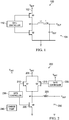
- FIG. 1 is a schematic diagram of a DC-to-DC voltage converter 100.
- the type of DC-to-DC voltage converter 100 depicted in FIG. 1 is sometimes referred to as a buck converter.
- the DC-to-DC voltage converter 100 includes a power stage that includes a high-side transistor Q1 and a low-side transistor Q2 that serve as switches.
- transistor Q1 is a p-channel transistor and transistor Q2 is an n-channel transistor.
- the source of transistor Q1 is coupled to a voltage input 102 that is couplable to a power supply VBAT.
- the voltage input 102 operates at an input voltage VBAT, which is a DC voltage that is to be converted to another DC voltage by the DC-to-DC voltage converter 100.
- the drain of transistor Q1 is coupled to a node N1.
- the drain of transistor Q2 is coupled to the node N1 and the source of transistor Q2 is coupled to a ground node.
- the ground node may operate at a potential of ground or a potential that is different than or lower than the input voltage VBAT. In the illustrative embodiment shown in FIG.
- the high-side transistor Q1 is a PMOS (p-channel metal-oxide-semiconductor field-effect) transistor
- the low-side transistor Q2 is an NMOS (n-channel metal-oxide-semiconductor field-effect) transistor, which constitutes a typical power stage for a DC-to-DC voltage converter.
- a first terminal of an inductor L1 is coupled to the node N1.
- the second terminal of the inductor L1 is coupled to a capacitor COUT.
- the junction of the inductor L1 and the capacitor COUT is the output 104 or output node of the DC-to-DC voltage converter 100, which operates at an output voltage VOUT.
- the voltage VOUT is the DC voltage generated by the DC-to-DC voltage converter 100.
- the gates of transistors Q1 and Q2 are coupled to a gate controller 110 that generates gate voltages to turn the transistors Q1 and Q2 off and on. Accordingly, the gate controller 110 serves as a switch controller to control the switching function of transistors Q1 and Q2.
- the DC-to-DC voltage converter 100 receives the input voltage VBAT at the input 102.
- the gate controller 110 turns transistors Q1 and Q2 off and on, so that one transistor is on while the other transistor is off.
- the off and on period controls the current IL flowing through the inductor L1.
- the current IL generates a voltage across the capacitor COUT, which is the output voltage VOUT of the DC-to-DC voltage converter 100. In discontinuous modes of operation, both transistor Q1 and transistor Q2 are turned off at the same time for a period.
- the power supply VBAT is provided by a battery power supply comprising one or more batteries.
- a battery power supply comprising one or more batteries.
- the PMOS transistor Q1 when VBAT is relatively low, i.e. close to the threshold voltage Vth of the PMOS transistor Q1, the PMOS transistor Q1 will exhibit a very high resistance, and will therefore not act like an effective switch.
- a DC-to-DC voltage converter 100 has a limited of range of operation with regards to the power supply voltage VBAT.
- the power transistors Q1 and Q2 used for devices that employ a 2AA cell power source are typically high voltage devices and would not conduct for 1AA cell voltage levels (which typically range from approximately 1V to 1.6V) due to the high threshold voltages of these transistors.
- Using low-voltage transistors for the power stage solves this conduction problem, but reliability related concerns would exist when the same device is expected to work from two AA cells.
- FIG. 2 is a schematic diagram of a DC-to-DC voltage converter 200 whose power stage includes a high-side switch that includes an n-channel transistor Q1 210 and a p-channel transistor Q2 215 in parallel.
- the illustrative embodiment depicted in FIG. 2 demonstrates aspects with respect to a buck DC-to-DC voltage converter, but the aspects that are described herein can also be implemented with other types of DC-to-DC converters, such as boost converters, buck-boost converters, flyback converters, and flybuck converters.
- the drain of n-channel transistor Q1 210 is coupled to a voltage input 205 that is couplable to a power supply VBAT.
- the source of p-channel transistor Q2 215 is also coupled to the voltage input 205.
- the voltage input 205 operates at the input voltage VBAT, which is a DC voltage that is to be converted to another DC voltage by the DC-to-DC voltage converter 200.
- the drain of the n-channel transistor Q1 210 and the source of the p-channel transistor 215 are both coupled to a node N1.
- the drain of n-channel transistor Q3 220 is coupled to the node N1 and the source of transistor Q3 220 is coupled to a ground node.
- the ground node may operate at a potential of ground or a potential that is different than or lower than the input voltage VBAT.
- the high-side n-channel transistor Q1 210 and the low-side n-channel transistor Q3 220 are NMOS transistors and the high-side p-channel transistor Q2 215 is a PMOS transistor.
- a first terminal of an inductor 225 is coupled to the node N1.
- the second terminal of the inductor 225 is coupled to an output capacitor 230.
- the junction of the inductor 225 and the output capacitor 230 is the output or output node of the DC-to-DC voltage converter 200, which operates at an output voltage VOUT.
- the voltage VOUT is the DC voltage generated by the DC-to-DC voltage converter 200.
- one of the high-side transistors serves as the active switch of the power stage of the DC-to-DC voltage converter 200 while the other high-side transistor is deactivated.
- the determination of which of the high-side transistors Q1 210 and Q2 215 to select as the active high-side switch is made by comparing the power supply voltage VBAT to a supply voltage threshold. If VBAT is less than the supply voltage threshold, the n-channel transistor Q1 210 serves as the active high-side transistor and the p-channel transistor Q2 215 is deactivated.
- the p-channel transistor Q2 215 is selected as the active high-side transistor and the n-channel transistor Q1 210 is deactivated.
- the n-channel transistor Q1 210 is the active high-side switch, thus allowing the high-side of the power stage to conduct at lower supply voltage levels.
- the p-channel transistor Q2 215 is the active high-side switch, thus offering the increased reliability that is associated with a higher-voltage device.
- the determination of which of the high-side transistors Q1 210 and Q2 215 to select as the active high-side switch is made by determining what type and how many batteries make up the power supply VBAT. For example, if the power supply VBAT consists of a single AA battery, the n-channel transistor Q1 210 serves as the active high-side transistor and the p-channel transistor Q2 215 is deactivated. Or, if the power supply VBAT consists of two AA batteries, the p-channel transistor Q2 215 is selected as the active high-side transistor, and the n-channel transistor Q1 210 is deactivated.
- the gates of the high-side n-channel transistor Q1 210, the high-side p-channel transistor Q2 215, and n-channel low-side transistor Q3 220 are coupled to a gate controller 235 that generates gate voltages to turn the transistors Q1 210, Q2 215 and Q3 220 on and off.
- the gate controller 235 serves as a switch controller to control the switching function of transistors Q1 210, Q2 215 and Q3 220.
- the gate control circuit 235 receives information regarding the power supply VBAT and, based on such information, controls one of the transistors Q1 210 and Q2 215 as the active high-side switch of the power stage and deactivates the other of the transistors Q1 210 and Q2 215.
- the gate control circuit 235 receives the supply voltage VBAT and compares it to a supply voltage threshold.
- the gate control circuit 235 includes a comparator for comparing the supply voltage VBAT to the supply voltage threshold.
- the gate control circuit 235 provides gate driver signals to the n-channel transistor Q1 210 and provides a voltage to the gate of p-channel transistor Q2 215 that turns off the p-channel transistor Q2 215.
- the p-channel transistor Q2 215 is deactivated and the n-channel transistor Q1 210 serves as the active transistor of the power stage when the supply voltage VBAT is less than the supply voltage threshold.
- the gate control circuit 235 provides gate driver signals to the p-channel transistor Q2 215 and provides a voltage to the gate of n-channel transistor Q1 210 that turns off the n-channel transistor Q1 210.
- the n-channel transistor Q1 210 is deactivated and the p-channel transistor Q2 215 serves as the active transistor of the power stage when the supply voltage VBAT is greater than the supply voltage threshold.
- the supply voltage threshold is set at a level that lies between the normal ranges of operation of a single-AA-cell power supply and a two-AA-cell power supply.
- the supply voltage threshold can be set at approximately 1.8 volts, which lies between the normal ranges of operation of a single AA cell (1.0-1.6 V) and two AA cells (2.0-3.2 V).
- the gate control circuit 235 receives or determines information regarding what type and how many batteries make up the power supply VBAT. For example, if the gate controller 235 determines, or receives information indicating, that the power supply VBAT consists of a single AA battery, the gate control circuit 235 provides gate driver signals to the n-channel transistor Q1 210 and provides a voltage to the gate of p-channel transistor Q2 215 that turns off the p-channel transistor Q2 215. Thus, the p-channel transistor Q2 215 is deactivated and the n-channel transistor Q1 210 serves as the active transistor of the power stage if the power supply VBAT consists of a single AA battery.
- the gate control circuit 235 determines, or receives information indicating, that the power supply VBAT consists of two AA batteries, the gate control circuit 235 provides gate driver signals to the p-channel transistor Q2 215 and provides a voltage to the gate of n-channel transistor Q1 210 that turns off the n-channel transistor Q1 210.
- the n-channel transistor Q1 210 is deactivated and the p-channel transistor Q2 215 serves as the active transistor of the power stage if the power supply VBAT consists of two AA batteries.
- n-channel transistor Q1 210 when n-channel transistor Q1 210 is the active high-side transistor of the DC-to-DC converter 200, i.e., when the power supply VBAT is a relatively lower-voltage power supply such as a single AA cell, the gate driver signal generated by the gate controller 235 for controlling the switching of the n-channel transistor Q1 210 is boosted using a charge pump circuit 245.
- This boosting of the gate driver signal causes the "on" voltage of the gate driver signal to be greater than the source voltage by an amount that is appreciably greater than the transistor voltage threshold Vth, thereby allowing the n-channel transistor Q1 210 to behave as an effective switch. If the magnitude of the gate driver signal is too low, as would be the case if the maximum level of the gate driver signal was substantially equal to a single AA cell voltage, the transistor Q1 210 does not behave as a switch.
- the transistors Q1 210, Q2 215, and Q3 220 are all implemented with thick gate oxide transistors, which are capable of handling 3.3 volts. Accordingly, all of these transistors are capable of working with either a single AA cell power supply or with a power supply consisting of two AA cells.
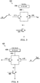
- FIG. 3 is a schematic diagram representing a power stage 300 of a DC-to-DC voltage converter, such as that shown in FIG. 2 , powered by a single AA cell power supply.
- the drain of n-channel transistor Q1 310 is coupled to a voltage input 305 that is connected to a power supply VBAT 308 that consists of a single AA cell.
- the source of p-channel transistor Q2 315 is also coupled to the voltage input 305.
- the drain of the n-channel transistor Q1 310 and the source of the p-channel transistor 315 are both coupled to a node N1.
- the drain of n-channel transistor Q3 320 is coupled to the node N1 and the source of transistor Q3 320 is coupled to a ground node. Though not shown in FIG.
- the node N1 is coupled to an output stage of the DC-to-DC power converter as shown in FIG. 2 .
- the gates of the high-side n-channel transistor Q1 310 and the high-side p-channel transistor Q2 315 are coupled to a gate control circuit such as gate controller 235 shown in FIG. 2 , although the gate control circuit is not explicitly shown in FIG. 3 .
- the gate control circuit 235 determines, based on information regarding the power supply VBAT 308, which of the high-side transistors Q1 310 and Q2 315 are to serve as the active high-side transistor of the power stage 300.
- this determination can be made in different ways, including comparing the power supply voltage VBAT to a supply voltage threshold (such as 1.8V), or by determining whether the power supply consists of one battery cell or two. In either case, when the power supply consists of a single AA battery as in FIG.
- the gate controller 235 will determine that the n-channel transistor Q1 310 is to serve as the active high-side transistor of the power stage 300. Based on that determination, the gate controller 235 deactivates, or turns off, the p-channel transistor Q2 315.
- the gate controller 235 turns off the p-channel transistor Q2 315 by applying a voltage that is substantially equal to VBAT to the gate of the p-channel transistor Q2 315.
- the source voltage Vs of transistor Q2 315 is substantially equal to the gate voltage Vg, in which case the p-channel transistor Q2 215 does not conduct any appreciable current.
- the gate controller actively controls the n-channel high-side transistor Q1 310 and the transistor Q3 320 by controlling the duty cycle of gate driver signals provided to Q1 310 and Q3 320.
- the voltage of the gate driver signal provided to the n-channel high-side transistor Q1 310 is boosted using the charge pump circuit 245 shown in FIG. 2 .
- the gate driver signal for transistor Q1 310 might be boosted to have a range from 0V on the low end to approximately 3V on the high end, as shown in FIG. 3 .
- This boosting of the gate driver signal for transistor Q1 310 allows for better performance of the high-side n-channel transistor Q1 310 in view of the relatively lower voltage level of the single AA cell power supply 308, as described with respect to FIG. 2 .
- FIG. 4 is a schematic diagram representing a power stage of DC-to-DC voltage converter such as that shown in FIG. 2 powered by two AA cells.
- the power stage 400 of FIG. 4 is substantially the same as that shown In FIGS. 3 and 4 except for the fact that the power supply VBAT 408 consists of two AA cells.
- the drain of n-channel transistor Q1 410 and the source of p-channel transistor Q2 415 are coupled to a voltage input 405 that is connected to the 2AA power supply VBAT 408.
- the source of the n-channel transistor Q1 410 and the drain of the p-channel transistor 415 are both coupled to a node N1.
- n-channel transistor Q3 420 The drain of n-channel transistor Q3 420 is coupled to the node N1 and the source of transistor Q3 420 is coupled to a ground node. Though not shown in FIG. 4 , the node N1 is coupled to an output stage of the DC-to-DC power converter as shown in FIG. 2 . Also, the gates of the high-side n-channel transistor Q1 410 and the high-side p-channel transistor Q2 415 are coupled to a gate control circuit such as gate controller 235 shown in FIG. 2 , although the gate control circuit is not explicitly shown in FIG. 4 .
- the gate control circuit 235 determines, based on information regarding the power supply VBAT 408, which of the high-side transistors Q1 410 and Q2 415 are to serve as the active high-side transistor of the power stage 400.
- this determination can be made in different ways, including comparing the power supply voltage VBAT to a supply voltage threshold (such as 1.8V), or by determining whether the power supply consists of one battery cell or two. In either case, when the power supply consists of two AA batteries as in FIG.
- the gate controller 235 will determine that the p-channel transistor Q2 410 is to serve as the active high-side transistor of the power stage 400. Based on that determination, the gate controller 235 deactivates, or turns off, the n-channel transistor Q1 410. In an illustrative embodiment, the gate controller 235 turns off the n-channel transistor Q1 410 by applying a voltage that is substantially equal to 0V to the gate of the n-channel transistor Q1 410. At the same time, the gate controller actively controls the p-channel high-side transistor Q2 415 and the transistor Q3 420 by controlling the duty cycle of gate driver signals provided to Q2 415 and Q3 420.
- FIG. 5 is a flow chart representing a method of operating a power stage of a DC-to-DC converter.
- a high-side n-channel transistor is provided.
- the drain terminal of the high-side n-channel transistor is coupled to a voltage input that is couplable to a power supply, and the source terminal is coupled to a first node that is couplable to an output stage of the DC-to-DC converter.
- a high-side p-channel transistor is provided.
- the source terminal of the high-side p-channel transistor is coupled to the voltage input and the drain terminal is coupled to the first node.
- the power supply voltage is compared to a threshold voltage level.
Description
- The increasing demand of integrating electronic devices onto automotive, industrial, and customer platforms requires more sophisticated power conversion and distribution designs. Often these electronic devices include embedded processors, memories, and other electronic components that are operated from one battery source. DC-to-DC voltage converters are used to supply different voltages to the different electronic device
- In pursuit of reducing the overall solution form factor for battery powered devices, an increasing trend is moving from two AA (2AA) cells (having a voltage range of approximately 2V to 3.2V) to a single AA (1AA) cell (having a voltage range of approximately 1V to 1.6V). The power stage for a typical DC-to-DC converter employs two field effect transistors (FETs) connected in series. The power transistors used for devices that employ a 2AA cell power source are usually high voltage devices (for reliability reasons) and would not conduct for 1AA cell voltage levels due to the high threshold voltages of these transistors. Using low-voltage transistors for the power stage solves this conduction problem, but reliability related concerns would exist when the same device is expected to work from two AA cells.
GB 2521704 - The invention is defined by the features of the appended claims. In a first embodiment, a power stage for a DC-to-DC converter is provided according to
claim 1. In detail, the power stage includes a voltage input, a high-side n-channel transistor, a high-side p-channel transistor, and a low-side n-channel transistor. The voltage input is couplable to a supply voltage. The drain terminal of the high-side n-channel transistor is coupled to the voltage input and the source terminal is coupled to a first node that is couplable to an output stage of the DC-to-DC converter. The source terminal of the high-side p-channel transistor is coupled to the voltage input and the drain terminal is coupled to the first node. The drain terminal of the low-side n-channel transistor is coupled to the first node and the source terminal is coupled to a ground. - In further embodiments, a DC-to-DC voltage converter includes a voltage input, a high-side n-channel transistor, a high-side p-channel transistor, a low-side n-channel transistor, an inductor, and a capacitor. The voltage input is couplable to a supply voltage. The drain terminal of the high-side n-channel transistor is coupled to the voltage input and the source terminal is coupled to a first node. The source terminal of the high-side p-channel transistor is coupled to the voltage input and the drain terminal is coupled to the first node. The drain terminal of the low-side n-channel transistor is coupled to the first node and the source terminal is coupled to a ground. The inductor is coupled between the first node and a converter output. The capacitor is coupled between the converter output and ground.
- In a further embodiment, according to claim 9, a method of operating a power stage of a DC-to-DC converter is provided.
-
-
FIG. 1 is a schematic diagram of a DC-to-DC voltage converter. -
FIG. 2 is a schematic diagram of a DC-to-DC voltage converter whose power stage includes a high-side switch that includes an n-channel transistor and a p-channel transistor coupled in parallel. -
FIG. 3 is a schematic diagram representing a power stage of DC-to-DC voltage converter such as that shown inFIG. 2 powered by a single AA cell power supply. -
FIG. 4 is a schematic diagram representing a power stage of DC-to-DC voltage converter such as that shown inFIG. 2 powered by two AA cells. -
FIG. 5 is a flow chart representing a method of operating a power stage of a DC-to-DC converter. -
FIG. 1 is a schematic diagram of a DC-to-DC voltage converter 100. The type of DC-to-DC voltage converter 100 depicted inFIG. 1 is sometimes referred to as a buck converter. The DC-to-DC voltage converter 100 includes a power stage that includes a high-side transistor Q1 and a low-side transistor Q2 that serve as switches. In the example ofFIG. 1 , transistor Q1 is a p-channel transistor and transistor Q2 is an n-channel transistor. The source of transistor Q1 is coupled to avoltage input 102 that is couplable to a power supply VBAT. During operation of the DC-to-DC voltage converter 100, thevoltage input 102 operates at an input voltage VBAT, which is a DC voltage that is to be converted to another DC voltage by the DC-to-DC voltage converter 100. The drain of transistor Q1 is coupled to a node N1. The drain of transistor Q2 is coupled to the node N1 and the source of transistor Q2 is coupled to a ground node. The ground node may operate at a potential of ground or a potential that is different than or lower than the input voltage VBAT. In the illustrative embodiment shown inFIG. 1 , the high-side transistor Q1 is a PMOS (p-channel metal-oxide-semiconductor field-effect) transistor, and the low-side transistor Q2 is an NMOS (n-channel metal-oxide-semiconductor field-effect) transistor, which constitutes a typical power stage for a DC-to-DC voltage converter. - A first terminal of an inductor L1 is coupled to the node N1. The second terminal of the inductor L1 is coupled to a capacitor COUT. The junction of the inductor L1 and the capacitor COUT is the
output 104 or output node of the DC-to-DC voltage converter 100, which operates at an output voltage VOUT. The voltage VOUT is the DC voltage generated by the DC-to-DC voltage converter 100. - The gates of transistors Q1 and Q2 are coupled to a
gate controller 110 that generates gate voltages to turn the transistors Q1 and Q2 off and on. Accordingly, thegate controller 110 serves as a switch controller to control the switching function of transistors Q1 and Q2. The DC-to-DC voltage converter 100 receives the input voltage VBAT at theinput 102. Thegate controller 110 turns transistors Q1 and Q2 off and on, so that one transistor is on while the other transistor is off. The off and on period controls the current IL flowing through the inductor L1. The current IL generates a voltage across the capacitor COUT, which is the output voltage VOUT of the DC-to-DC voltage converter 100. In discontinuous modes of operation, both transistor Q1 and transistor Q2 are turned off at the same time for a period. - In many implementations, the power supply VBAT is provided by a battery power supply comprising one or more batteries. In implementations such as the one shown in
FIG. 1 , wherein a PMOS transistor Q1 is used as the high-side switch, when VBAT is relatively low, i.e. close to the threshold voltage Vth of the PMOS transistor Q1, the PMOS transistor Q1 will exhibit a very high resistance, and will therefore not act like an effective switch. Thus such a DC-to-DC voltage converter 100 has a limited of range of operation with regards to the power supply voltage VBAT. The power transistors Q1 and Q2 used for devices that employ a 2AA cell power source (having a voltage range of approximately 2V to 3.2V) are typically high voltage devices and would not conduct for 1AA cell voltage levels (which typically range from approximately 1V to 1.6V) due to the high threshold voltages of these transistors. Using low-voltage transistors for the power stage solves this conduction problem, but reliability related concerns would exist when the same device is expected to work from two AA cells. -
FIG. 2 is a schematic diagram of a DC-to-DC voltage converter 200 whose power stage includes a high-side switch that includes an n-channel transistor Q1 210 and a p-channel transistor Q2 215 in parallel. The illustrative embodiment depicted inFIG. 2 demonstrates aspects with respect to a buck DC-to-DC voltage converter, but the aspects that are described herein can also be implemented with other types of DC-to-DC converters, such as boost converters, buck-boost converters, flyback converters, and flybuck converters. The drain of n-channel transistor Q1 210 is coupled to avoltage input 205 that is couplable to a power supply VBAT. The source of p-channel transistor Q2 215 is also coupled to thevoltage input 205. During operation of the DC-to-DC voltage converter 200, thevoltage input 205 operates at the input voltage VBAT, which is a DC voltage that is to be converted to another DC voltage by the DC-to-DC voltage converter 200. The drain of the n-channel transistor Q1 210 and the source of the p-channel transistor 215 are both coupled to a node N1. The drain of n-channel transistor Q3 220 is coupled to the node N1 and the source oftransistor Q3 220 is coupled to a ground node. The ground node may operate at a potential of ground or a potential that is different than or lower than the input voltage VBAT. In the illustrative embodiment shown inFIG. 2 , the high-side n-channel transistor Q1 210 and the low-side n-channel transistor Q3 220 are NMOS transistors and the high-side p-channel transistor Q2 215 is a PMOS transistor. - A first terminal of an
inductor 225 is coupled to the node N1. The second terminal of theinductor 225 is coupled to anoutput capacitor 230. The junction of theinductor 225 and theoutput capacitor 230 is the output or output node of the DC-to-DC voltage converter 200, which operates at an output voltage VOUT. The voltage VOUT is the DC voltage generated by the DC-to-DC voltage converter 200. - Depending on the voltage level of the power supply VBAT, one of the high-side transistors, either n-
channel transistor Q1 210 or p-channel transistor Q2 215, serves as the active switch of the power stage of the DC-to-DC voltage converter 200 while the other high-side transistor is deactivated. In an illustrative embodiment, the determination of which of the high-side transistors Q1 210 andQ2 215 to select as the active high-side switch is made by comparing the power supply voltage VBAT to a supply voltage threshold. If VBAT is less than the supply voltage threshold, the n-channel transistor Q1 210 serves as the active high-side transistor and the p-channel transistor Q2 215 is deactivated. If VBAT is greater than the supply voltage threshold, the p-channel transistor Q2 215 is selected as the active high-side transistor and the n-channel transistor Q1 210 is deactivated. Thus, when the power supply voltage VBAT is less than the supply voltage threshold, the n-channel transistor Q1 210 is the active high-side switch, thus allowing the high-side of the power stage to conduct at lower supply voltage levels. And when the power supply voltage VBAT is greater than the supply voltage threshold, the p-channel transistor Q2 215 is the active high-side switch, thus offering the increased reliability that is associated with a higher-voltage device. - In an alternative embodiment, the determination of which of the high-
side transistors Q1 210 andQ2 215 to select as the active high-side switch is made by determining what type and how many batteries make up the power supply VBAT. For example, if the power supply VBAT consists of a single AA battery, the n-channel transistor Q1 210 serves as the active high-side transistor and the p-channel transistor Q2 215 is deactivated. Or, if the power supply VBAT consists of two AA batteries, the p-channel transistor Q2 215 is selected as the active high-side transistor, and the n-channel transistor Q1 210 is deactivated. - The gates of the high-side n-
channel transistor Q1 210, the high-side p-channel transistor Q2 215, and n-channel low-side transistor Q3 220 are coupled to agate controller 235 that generates gate voltages to turn thetransistors Q1 210,Q2 215 andQ3 220 on and off. Thus, thegate controller 235 serves as a switch controller to control the switching function oftransistors Q1 210,Q2 215 andQ3 220. - The
gate control circuit 235 receives information regarding the power supply VBAT and, based on such information, controls one of thetransistors Q1 210 andQ2 215 as the active high-side switch of the power stage and deactivates the other of thetransistors Q1 210 andQ2 215. For example, in an illustrative embodiment, thegate control circuit 235 receives the supply voltage VBAT and compares it to a supply voltage threshold. In an illustrative embodiment thegate control circuit 235 includes a comparator for comparing the supply voltage VBAT to the supply voltage threshold. If VBAT is less than the supply voltage threshold, thegate control circuit 235 provides gate driver signals to the n-channel transistor Q1 210 and provides a voltage to the gate of p-channel transistor Q2 215 that turns off the p-channel transistor Q2 215. Thus, the p-channel transistor Q2 215 is deactivated and the n-channel transistor Q1 210 serves as the active transistor of the power stage when the supply voltage VBAT is less than the supply voltage threshold. If VBAT is greater than the supply voltage threshold, thegate control circuit 235 provides gate driver signals to the p-channel transistor Q2 215 and provides a voltage to the gate of n-channel transistor Q1 210 that turns off the n-channel transistor Q1 210. Thus, the n-channel transistor Q1 210 is deactivated and the p-channel transistor Q2 215 serves as the active transistor of the power stage when the supply voltage VBAT is greater than the supply voltage threshold. - In an illustrative implementation wherein the DC-to-
DC converter 200 is intended to be compatible with both a power supply comprising a single AA cell and a power supply comprising two AA cells, the supply voltage threshold is set at a level that lies between the normal ranges of operation of a single-AA-cell power supply and a two-AA-cell power supply. For example, the supply voltage threshold can be set at approximately 1.8 volts, which lies between the normal ranges of operation of a single AA cell (1.0-1.6 V) and two AA cells (2.0-3.2 V). - In an alternative embodiment, the
gate control circuit 235 receives or determines information regarding what type and how many batteries make up the power supply VBAT. For example, if thegate controller 235 determines, or receives information indicating, that the power supply VBAT consists of a single AA battery, thegate control circuit 235 provides gate driver signals to the n-channel transistor Q1 210 and provides a voltage to the gate of p-channel transistor Q2 215 that turns off the p-channel transistor Q2 215. Thus, the p-channel transistor Q2 215 is deactivated and the n-channel transistor Q1 210 serves as the active transistor of the power stage if the power supply VBAT consists of a single AA battery. Or, if thegate controller 235 determines, or receives information indicating, that the power supply VBAT consists of two AA batteries, thegate control circuit 235 provides gate driver signals to the p-channel transistor Q2 215 and provides a voltage to the gate of n-channel transistor Q1 210 that turns off the n-channel transistor Q1 210. Thus, the n-channel transistor Q1 210 is deactivated and the p-channel transistor Q2 215 serves as the active transistor of the power stage if the power supply VBAT consists of two AA batteries. - In an illustrative embodiment, when n-
channel transistor Q1 210 is the active high-side transistor of the DC-to-DC converter 200, i.e., when the power supply VBAT is a relatively lower-voltage power supply such as a single AA cell, the gate driver signal generated by thegate controller 235 for controlling the switching of the n-channel transistor Q1 210 is boosted using acharge pump circuit 245. This boosting of the gate driver signal causes the "on" voltage of the gate driver signal to be greater than the source voltage by an amount that is appreciably greater than the transistor voltage threshold Vth, thereby allowing the n-channel transistor Q1 210 to behave as an effective switch. If the magnitude of the gate driver signal is too low, as would be the case if the maximum level of the gate driver signal was substantially equal to a single AA cell voltage, thetransistor Q1 210 does not behave as a switch. - In illustrative embodiments, the
transistors Q1 210,Q2 215, andQ3 220 are all implemented with thick gate oxide transistors, which are capable of handling 3.3 volts. Accordingly, all of these transistors are capable of working with either a single AA cell power supply or with a power supply consisting of two AA cells. -
FIG. 3 is a schematic diagram representing apower stage 300 of a DC-to-DC voltage converter, such as that shown inFIG. 2 , powered by a single AA cell power supply. The drain of n-channel transistor Q1 310 is coupled to avoltage input 305 that is connected to apower supply VBAT 308 that consists of a single AA cell. The source of p-channel transistor Q2 315 is also coupled to thevoltage input 305. The drain of the n-channel transistor Q1 310 and the source of the p-channel transistor 315 are both coupled to a node N1. The drain of n-channel transistor Q3 320 is coupled to the node N1 and the source oftransistor Q3 320 is coupled to a ground node. Though not shown inFIG. 3 , the node N1 is coupled to an output stage of the DC-to-DC power converter as shown inFIG. 2 . Also, the gates of the high-side n-channel transistor Q1 310 and the high-side p-channel transistor Q2 315 are coupled to a gate control circuit such asgate controller 235 shown inFIG. 2 , although the gate control circuit is not explicitly shown inFIG. 3 . - The
gate control circuit 235 determines, based on information regarding thepower supply VBAT 308, which of the high-side transistors Q1 310 andQ2 315 are to serve as the active high-side transistor of thepower stage 300. In the illustrative embodiment ofFIGS. 3 and 4 , wherein the DC-to-DC converter is intended to be compatible with both a power supply comprising a single AA cell and a power supply comprising two AA cells, this determination can be made in different ways, including comparing the power supply voltage VBAT to a supply voltage threshold (such as 1.8V), or by determining whether the power supply consists of one battery cell or two. In either case, when the power supply consists of a single AA battery as inFIG. 3 , thegate controller 235 will determine that the n-channel transistor Q1 310 is to serve as the active high-side transistor of thepower stage 300. Based on that determination, thegate controller 235 deactivates, or turns off, the p-channel transistor Q2 315. - In an illustrative embodiment, the
gate controller 235 turns off the p-channel transistor Q2 315 by applying a voltage that is substantially equal to VBAT to the gate of the p-channel transistor Q2 315. In that event, the source voltage Vs oftransistor Q2 315 is substantially equal to the gate voltage Vg, in which case the p-channel transistor Q2 215 does not conduct any appreciable current. At the same time, the gate controller actively controls the n-channel high-side transistor Q1 310 and thetransistor Q3 320 by controlling the duty cycle of gate driver signals provided toQ1 310 andQ3 320. - In an illustrative embodiment, the voltage of the gate driver signal provided to the n-channel high-
side transistor Q1 310 is boosted using thecharge pump circuit 245 shown inFIG. 2 . For example, the gate driver signal fortransistor Q1 310 might be boosted to have a range from 0V on the low end to approximately 3V on the high end, as shown inFIG. 3 . This boosting of the gate driver signal fortransistor Q1 310 allows for better performance of the high-side n-channel transistor Q1 310 in view of the relatively lower voltage level of the single AAcell power supply 308, as described with respect toFIG. 2 . -
FIG. 4 is a schematic diagram representing a power stage of DC-to-DC voltage converter such as that shown inFIG. 2 powered by two AA cells. Thepower stage 400 ofFIG. 4 is substantially the same as that shown InFIGS. 3 and 4 except for the fact that thepower supply VBAT 408 consists of two AA cells. The drain of n-channel transistor Q1 410 and the source of p-channel transistor Q2 415 are coupled to avoltage input 405 that is connected to the 2AApower supply VBAT 408. The source of the n-channel transistor Q1 410 and the drain of the p-channel transistor 415 are both coupled to a node N1. The drain of n-channel transistor Q3 420 is coupled to the node N1 and the source oftransistor Q3 420 is coupled to a ground node. Though not shown inFIG. 4 , the node N1 is coupled to an output stage of the DC-to-DC power converter as shown inFIG. 2 . Also, the gates of the high-side n-channel transistor Q1 410 and the high-side p-channel transistor Q2 415 are coupled to a gate control circuit such asgate controller 235 shown inFIG. 2 , although the gate control circuit is not explicitly shown inFIG. 4 . - As described hereinabove, the
gate control circuit 235 determines, based on information regarding thepower supply VBAT 408, which of the high-side transistors Q1 410 andQ2 415 are to serve as the active high-side transistor of thepower stage 400. In the illustrative embodiment ofFIGS. 3 and 4 , wherein the DC-to-DC converter is intended to be compatible with both a power supply comprising a single AA cell and a power supply comprising two AA cells, this determination can be made in different ways, including comparing the power supply voltage VBAT to a supply voltage threshold (such as 1.8V), or by determining whether the power supply consists of one battery cell or two. In either case, when the power supply consists of two AA batteries as inFIG. 4 , thegate controller 235 will determine that the p-channel transistor Q2 410 is to serve as the active high-side transistor of thepower stage 400. Based on that determination, thegate controller 235 deactivates, or turns off, the n-channel transistor Q1 410. In an illustrative embodiment, thegate controller 235 turns off the n-channel transistor Q1 410 by applying a voltage that is substantially equal to 0V to the gate of the n-channel transistor Q1 410. At the same time, the gate controller actively controls the p-channel high-side transistor Q2 415 and thetransistor Q3 420 by controlling the duty cycle of gate driver signals provided toQ2 415 andQ3 420. -
FIG. 5 is a flow chart representing a method of operating a power stage of a DC-to-DC converter. Atblock 500, a high-side n-channel transistor is provided. The drain terminal of the high-side n-channel transistor is coupled to a voltage input that is couplable to a power supply, and the source terminal is coupled to a first node that is couplable to an output stage of the DC-to-DC converter. At block 510, a high-side p-channel transistor is provided. The source terminal of the high-side p-channel transistor is coupled to the voltage input and the drain terminal is coupled to the first node. Atblock 520, the power supply voltage is compared to a threshold voltage level. Atdecision block 530, a determination is made about whether the power supply voltage VBAT is greater than the power supply voltage threshold Vth. If the power supply voltage VBAT is greater than the threshold voltage Vth, the high-side n-channel transistor is deactivated, as shown atblock 540, and the high-side p-channel transistor is caused to serve as the active high-side transistor of the DC-to-DC converter, as shown atblock 550. If the power supply voltage VBAT is less than the threshold voltage Vth, the high-side p-channel transistor is deactivated, as shown atblock 560, and the high-side n-channel transistor is caused to serve as the active high-side transistor of the DC-to-DC converter, as shown atblock 570. - Accordingly, examples of DC-to-DC voltage converter power stages and methods for operating a power stage of a DC-to-DC voltage converter have been described in detail herein.
- Modifications are possible in the described embodiments, and other embodiments are possible, within the scope of the claims.
Claims (12)
- A power stage for a DC-to-DC voltage converter, the power stage comprising:a voltage input configured to be coupled to a supply voltage (205);a high-side n-channel transistor (210) comprising a source terminal, a drain terminal and a gate terminal, the drain terminal being coupled to the voltage input and the source terminal being coupled to a first node (N1) that is configured to be coupled to an output stage of the DC-to-DC converter;a high-side p-channel transistor (215) comprising a source terminal, a drain terminal and a gate terminal, the source terminal being coupled to the voltage input and the drain terminal being coupled to the first node; anda low-side n-channel transistor (220) comprising a source terminal, a drain terminal and a gate terminal, the drain terminal being coupled to the first node and the source terminal being coupled to a ground;control circuitry (235) configured to receive information regarding the supply voltage (205) and configured to cause the high-side n-channel transistor (210) to serve as the active high-side transistor of the DC-to-DC converter, while deactivating the high-side p-channel transistor (215), if the supply voltage (205) is below a predetermined threshold value (Vth), and configured to cause the high-side p-channel transistor (210) to serve as the active high-side transistor of the DC-to-DC converter, while deactivating the high-side n-channel transistor (215), if the supply voltage (205) is above the predetermined threshold value.
- A DC-to-DC voltage converter comprising a power stage according to claim 1 and:an inductor (225) coupled between the first node and a converter output; anda capacitor (230) coupled between the converter output and ground.
- The power stage or DC-to-DC voltage converter of claim 1, wherein if the supply voltage (205) is below the predetermined threshold voltage, the control circuit is configured to provide a constant voltage that is substantially equal to the supply voltage (205) to the gate of the high-side p-channel transistor (215), thereby deactivating the high-side p-channel transistor (215), and configured to regulate the duty cycle of a gate driver signal provided to the gate of the high-side n-channel transistor (210) in order to regulate an output voltage of the DC-to-DC converter.
- The power stage or DC-to-DC voltage converter of claim 3, further comprising a charge pump circuit (245) configured to boost the voltage of the gate driver signal that is provided to the gate of the high-side n-channel transistor (210).
- The power stage or DC-to-DC voltage converter of claim 3, wherein if the supply voltage (205) is above the predetermined threshold voltage, the control circuit is configured to provide a constant voltage that is substantially equal to 0 volts to the gate of the high-side n-channel transistor (210), thereby deactivating the high-side n-channel transistor (210), and configured to regulate the duty cycle of a gate driver signal provided to the gate of the high-side p-channel transistor (215) in order to regulate an output voltage of the DC-to-DC converter.
- The power stage of claim 1 or the DC-to-DC voltage converter of claim 2, wherein the control circuitry (235) is configured to cause the high-side n-channel transistor (210) to serve as the active high-side transistor of the DC-to-DC converter, while deactivating the high-side p-channel transistor (215), if the power supply comprises a first number of batteries of a given type, and operable to cause the high-side n-channel transistor (210) to serve as the active high-side transistor of the DC-to-DC converter, while deactivating the high-side p-channel transistor (215), if the power supply comprises a second number of batteries of a given type.
- The power stage or DC-to-DC voltage converter of claim 6, wherein the given type of battery comprises a AA cell, the first number of batteries comprises a single battery, and the second number of batteries comprises two batteries.
- The power stage of claim 1 or the DC-to-DC voltage converter of claim 2 wherein the high-side n-channel transistor (210) comprises an NMOS transistor, and the high-side p-channel transistor (215) comprises a PMOS transistor.
- A method of operating a power stage of a DC-to-DC converter, comprising:providing a high-side n-channel transistor (210) comprising a source terminal, a drain terminal and a gate terminal, the drain terminal being coupled to a voltage input that is coupled to a power supply, and the source terminal being coupled to a first node that is couplable to an output stage of the DC-to-DC converter;providing a high-side p-channel transistor (215) comprising a source terminal, a drain terminal and a gate terminal, the source terminal being coupled to the voltage input and the drain terminal being coupled to the first node;comparing the power supply voltage (205) to a threshold voltage level (Vth);if the power supply voltage (205) is less than the threshold voltage level, causing the high-side n-channel transistor (210) to serve as the active high-side transistor of the DC-to-DC converter, and deactivating the high-side p-channel transistor (215);if the power supply voltage (205) is greater than the threshold voltage level, causing the high-side p-channel transistor (215) to serve as the active high-side transistor of the DC-to-DC converter, and deactivating the high-side n-channel transistor (210).
- The method of claim 9, further comprising:
if the power supply voltage (205) is less than the predetermined threshold voltage, providing a constant voltage that is substantially equal to the supply voltage (205) to the gate of the high-side p-channel transistor (215), thereby deactivating the high-side p-channel transistor (215), and regulating the duty cycle of a gate driver signal provided to the gate of the high-side n-channel transistor (210) in order to regulate an output voltage of the DC-to-DC converter. - The method of claim 10, further comprising boosting, using a charge pump (245), the voltage of the gate driver signal that is provided to the gate of the high-side n-channel transistor (210).
- The method of claim 11, further comprising:
if the power supply voltage (205) is greater than the predetermined threshold voltage, providing a constant voltage that is substantially equal to 0 volts to the gate of the high-side n-channel transistor (210), thereby deactivating the high-side n-channel transistor (210), and regulating the duty cycle of a gate driver signal provided to the gate of the high-side p-channel transistor (215) in order to regulate an output voltage of the DC-to-DC converter.
Applications Claiming Priority (2)
| Application Number | Priority Date | Filing Date | Title |
|---|---|---|---|
| US15/160,836 US9882490B2 (en) | 2016-05-20 | 2016-05-20 | Parallel high side switches for a buck converter |
| PCT/US2017/033844 WO2017201533A1 (en) | 2016-05-20 | 2017-05-22 | Power stage for a dc-dc converter |
Publications (3)
| Publication Number | Publication Date |
|---|---|
| EP3459167A1 EP3459167A1 (en) | 2019-03-27 |
| EP3459167A4 EP3459167A4 (en) | 2019-05-08 |
| EP3459167B1 true EP3459167B1 (en) | 2021-09-08 |
Family
ID=60326611
Family Applications (1)
| Application Number | Title | Priority Date | Filing Date |
|---|---|---|---|
| EP17800335.6A Active EP3459167B1 (en) | 2016-05-20 | 2017-05-22 | Power stage for a dc-dc converter |
Country Status (6)
| Country | Link |
|---|---|
| US (1) | US9882490B2 (en) |
| EP (1) | EP3459167B1 (en) |
| JP (1) | JP2019517238A (en) |
| KR (1) | KR20190007430A (en) |
| CN (1) | CN109155588A (en) |
| WO (1) | WO2017201533A1 (en) |
Families Citing this family (1)
| Publication number | Priority date | Publication date | Assignee | Title |
|---|---|---|---|---|
| US11095282B2 (en) * | 2018-12-05 | 2021-08-17 | Texas Instruments Incorporated | Methods and apparatus to implement current limit test mode |
Family Cites Families (12)
| Publication number | Priority date | Publication date | Assignee | Title |
|---|---|---|---|---|
| JP3036457B2 (en) | 1997-02-27 | 2000-04-24 | 日本電気株式会社 | Switching power supply |
| US7737666B2 (en) * | 2003-08-04 | 2010-06-15 | Marvell World Trade Ltd. | Split gate drive scheme to improve reliable voltage operation range |
| US20080007236A1 (en) * | 2006-07-06 | 2008-01-10 | Alan Elbanhawy | Power converter with segmented power module |
| JP5029156B2 (en) * | 2007-06-11 | 2012-09-19 | 富士通セミコンダクター株式会社 | DC-DC converter and control method thereof |
| JP5326421B2 (en) * | 2008-08-18 | 2013-10-30 | 富士電機株式会社 | Abnormal current prevention circuit for DC-DC converter |
| JP5616104B2 (en) * | 2010-04-12 | 2014-10-29 | 株式会社マキタ | Power tools powered by battery packs and their adapters |
| JP5998739B2 (en) * | 2012-08-20 | 2016-09-28 | 富士通株式会社 | Regulator device |
| EP2730931B1 (en) * | 2012-11-12 | 2015-08-26 | ST-Ericsson SA | Absolute value current-sensing circuit for step-down DC-to-DC converters with integrated power stage |
| JP5937503B2 (en) * | 2012-12-26 | 2016-06-22 | ルネサスエレクトロニクス株式会社 | Semiconductor integrated circuit and operation method thereof |
| CN103401423B (en) | 2013-07-29 | 2015-07-29 | 电子科技大学 | A kind of adaptive segmentation drives DC-DC converter |
| US9369033B2 (en) | 2013-12-30 | 2016-06-14 | Qualcomm Technologies International, Ltd. | Low power switched mode power supply |
| EP2933912A1 (en) | 2014-04-16 | 2015-10-21 | Dialog Semiconductor GmbH | Overvoltage reduction in buck converter operating in PFM mode |
-
2016
- 2016-05-20 US US15/160,836 patent/US9882490B2/en not_active Expired - Fee Related
-
2017
- 2017-05-22 KR KR1020187033131A patent/KR20190007430A/en not_active Application Discontinuation
- 2017-05-22 JP JP2018561004A patent/JP2019517238A/en active Pending
- 2017-05-22 EP EP17800335.6A patent/EP3459167B1/en active Active
- 2017-05-22 WO PCT/US2017/033844 patent/WO2017201533A1/en unknown
- 2017-05-22 CN CN201780030175.9A patent/CN109155588A/en active Pending
Also Published As
| Publication number | Publication date |
|---|---|
| KR20190007430A (en) | 2019-01-22 |
| US20170338742A1 (en) | 2017-11-23 |
| JP2019517238A (en) | 2019-06-20 |
| EP3459167A4 (en) | 2019-05-08 |
| CN109155588A (en) | 2019-01-04 |
| US9882490B2 (en) | 2018-01-30 |
| EP3459167A1 (en) | 2019-03-27 |
| WO2017201533A1 (en) | 2017-11-23 |
Similar Documents
| Publication | Publication Date | Title |
|---|---|---|
| US10008932B2 (en) | Synchronous rectification DC/DC converter | |
| US9577520B2 (en) | Power converter with bootstrap circuit | |
| US10498229B2 (en) | Method and circuitry to soft start high power charge pumps | |
| US6812782B2 (en) | Switch mode converter that allows 100% duty cycle on gate driver | |
| US10243467B2 (en) | Voltage regulators with kickback protection | |
| US7298117B2 (en) | Step-up (boost) DC regulator with two-level back-bias switch gate voltage | |
| US9106228B2 (en) | Adaptive MOS transistor gate driver and method therefor | |
| US8004254B2 (en) | Power supply circuit | |
| US20070210774A1 (en) | Switching power supply circuitry | |
| US8299765B2 (en) | Power supply control device and power supply control method | |
| US20090153122A1 (en) | Dropper-type regulator | |
| US7528589B2 (en) | Step-up DC/DC converter and electronic appliance therewith | |
| WO2007010801A1 (en) | Step-up/down switching regulator, its control circuit, and electronic apparatus using same | |
| US9178408B2 (en) | Voltage regulators with load-dependent bias | |
| JP2014023272A (en) | Switching power-supply circuit | |
| US20160268885A1 (en) | Using PMOS Power Switch In A Combination Switching And Linear Regulator | |
| CN108336895B (en) | DC-DC converter, DC-DC power conversion system and method | |
| JP6831713B2 (en) | Bootstrap circuit | |
| US10268221B2 (en) | Power supply device and electronic control unit for lowering a minimum operating voltage and suppressing a consumed current to be low | |
| EP3459167B1 (en) | Power stage for a dc-dc converter | |
| JP2007189771A (en) | Power unit | |
| US10811972B2 (en) | Buck-boost converter power supply with drive circuit | |
| TWI710202B (en) | Switching regulator | |
| US6104173A (en) | DC-DC converter and power-supply switching circuit | |
| US11641162B2 (en) | Circuits and methods for generating a supply voltage for a switching regulator |
Legal Events
| Date | Code | Title | Description |
|---|---|---|---|
| STAA | Information on the status of an ep patent application or granted ep patent |
Free format text: STATUS: THE INTERNATIONAL PUBLICATION HAS BEEN MADE |
|
| PUAI | Public reference made under article 153(3) epc to a published international application that has entered the european phase |
Free format text: ORIGINAL CODE: 0009012 |
|
| STAA | Information on the status of an ep patent application or granted ep patent |
Free format text: STATUS: REQUEST FOR EXAMINATION WAS MADE |
|
| 17P | Request for examination filed |
Effective date: 20181220 |
|
| AK | Designated contracting states |
Kind code of ref document: A1 Designated state(s): AL AT BE BG CH CY CZ DE DK EE ES FI FR GB GR HR HU IE IS IT LI LT LU LV MC MK MT NL NO PL PT RO RS SE SI SK SM TR |
|
| AX | Request for extension of the european patent |
Extension state: BA ME |
|
| STAA | Information on the status of an ep patent application or granted ep patent |
Free format text: STATUS: REQUEST FOR EXAMINATION WAS MADE |
|
| A4 | Supplementary search report drawn up and despatched |
Effective date: 20190408 |
|
| RIC1 | Information provided on ipc code assigned before grant |
Ipc: H02M 3/158 20060101AFI20190402BHEP |
|
| DAV | Request for validation of the european patent (deleted) | ||
| DAX | Request for extension of the european patent (deleted) | ||
| GRAP | Despatch of communication of intention to grant a patent |
Free format text: ORIGINAL CODE: EPIDOSNIGR1 |
|
| STAA | Information on the status of an ep patent application or granted ep patent |
Free format text: STATUS: GRANT OF PATENT IS INTENDED |
|
| INTG | Intention to grant announced |
Effective date: 20210429 |
|
| GRAS | Grant fee paid |
Free format text: ORIGINAL CODE: EPIDOSNIGR3 |
|
| GRAA | (expected) grant |
Free format text: ORIGINAL CODE: 0009210 |
|
| STAA | Information on the status of an ep patent application or granted ep patent |
Free format text: STATUS: THE PATENT HAS BEEN GRANTED |
|
| AK | Designated contracting states |
Kind code of ref document: B1 Designated state(s): AL AT BE BG CH CY CZ DE DK EE ES FI FR GB GR HR HU IE IS IT LI LT LU LV MC MK MT NL NO PL PT RO RS SE SI SK SM TR |
|
| REG | Reference to a national code |
Ref country code: GB Ref legal event code: FG4D |
|
| REG | Reference to a national code |
Ref country code: AT Ref legal event code: REF Ref document number: 1429458 Country of ref document: AT Kind code of ref document: T Effective date: 20210915 Ref country code: CH Ref legal event code: EP |
|
| REG | Reference to a national code |
Ref country code: IE Ref legal event code: FG4D |
|
| REG | Reference to a national code |
Ref country code: DE Ref legal event code: R096 Ref document number: 602017045757 Country of ref document: DE |
|
| REG | Reference to a national code |
Ref country code: LT Ref legal event code: MG9D |
|
| REG | Reference to a national code |
Ref country code: NL Ref legal event code: MP Effective date: 20210908 |
|
| PG25 | Lapsed in a contracting state [announced via postgrant information from national office to epo] |
Ref country code: HR Free format text: LAPSE BECAUSE OF FAILURE TO SUBMIT A TRANSLATION OF THE DESCRIPTION OR TO PAY THE FEE WITHIN THE PRESCRIBED TIME-LIMIT Effective date: 20210908 Ref country code: FI Free format text: LAPSE BECAUSE OF FAILURE TO SUBMIT A TRANSLATION OF THE DESCRIPTION OR TO PAY THE FEE WITHIN THE PRESCRIBED TIME-LIMIT Effective date: 20210908 Ref country code: ES Free format text: LAPSE BECAUSE OF FAILURE TO SUBMIT A TRANSLATION OF THE DESCRIPTION OR TO PAY THE FEE WITHIN THE PRESCRIBED TIME-LIMIT Effective date: 20210908 Ref country code: SE Free format text: LAPSE BECAUSE OF FAILURE TO SUBMIT A TRANSLATION OF THE DESCRIPTION OR TO PAY THE FEE WITHIN THE PRESCRIBED TIME-LIMIT Effective date: 20210908 Ref country code: RS Free format text: LAPSE BECAUSE OF FAILURE TO SUBMIT A TRANSLATION OF THE DESCRIPTION OR TO PAY THE FEE WITHIN THE PRESCRIBED TIME-LIMIT Effective date: 20210908 Ref country code: BG Free format text: LAPSE BECAUSE OF FAILURE TO SUBMIT A TRANSLATION OF THE DESCRIPTION OR TO PAY THE FEE WITHIN THE PRESCRIBED TIME-LIMIT Effective date: 20211208 Ref country code: LT Free format text: LAPSE BECAUSE OF FAILURE TO SUBMIT A TRANSLATION OF THE DESCRIPTION OR TO PAY THE FEE WITHIN THE PRESCRIBED TIME-LIMIT Effective date: 20210908 Ref country code: NO Free format text: LAPSE BECAUSE OF FAILURE TO SUBMIT A TRANSLATION OF THE DESCRIPTION OR TO PAY THE FEE WITHIN THE PRESCRIBED TIME-LIMIT Effective date: 20211208 |
|
| REG | Reference to a national code |
Ref country code: AT Ref legal event code: MK05 Ref document number: 1429458 Country of ref document: AT Kind code of ref document: T Effective date: 20210908 |
|
| PG25 | Lapsed in a contracting state [announced via postgrant information from national office to epo] |
Ref country code: LV Free format text: LAPSE BECAUSE OF FAILURE TO SUBMIT A TRANSLATION OF THE DESCRIPTION OR TO PAY THE FEE WITHIN THE PRESCRIBED TIME-LIMIT Effective date: 20210908 Ref country code: GR Free format text: LAPSE BECAUSE OF FAILURE TO SUBMIT A TRANSLATION OF THE DESCRIPTION OR TO PAY THE FEE WITHIN THE PRESCRIBED TIME-LIMIT Effective date: 20211209 |
|
| PG25 | Lapsed in a contracting state [announced via postgrant information from national office to epo] |
Ref country code: AT Free format text: LAPSE BECAUSE OF FAILURE TO SUBMIT A TRANSLATION OF THE DESCRIPTION OR TO PAY THE FEE WITHIN THE PRESCRIBED TIME-LIMIT Effective date: 20210908 |
|
| PG25 | Lapsed in a contracting state [announced via postgrant information from national office to epo] |
Ref country code: IS Free format text: LAPSE BECAUSE OF FAILURE TO SUBMIT A TRANSLATION OF THE DESCRIPTION OR TO PAY THE FEE WITHIN THE PRESCRIBED TIME-LIMIT Effective date: 20220108 Ref country code: SM Free format text: LAPSE BECAUSE OF FAILURE TO SUBMIT A TRANSLATION OF THE DESCRIPTION OR TO PAY THE FEE WITHIN THE PRESCRIBED TIME-LIMIT Effective date: 20210908 Ref country code: SK Free format text: LAPSE BECAUSE OF FAILURE TO SUBMIT A TRANSLATION OF THE DESCRIPTION OR TO PAY THE FEE WITHIN THE PRESCRIBED TIME-LIMIT Effective date: 20210908 Ref country code: RO Free format text: LAPSE BECAUSE OF FAILURE TO SUBMIT A TRANSLATION OF THE DESCRIPTION OR TO PAY THE FEE WITHIN THE PRESCRIBED TIME-LIMIT Effective date: 20210908 Ref country code: PT Free format text: LAPSE BECAUSE OF FAILURE TO SUBMIT A TRANSLATION OF THE DESCRIPTION OR TO PAY THE FEE WITHIN THE PRESCRIBED TIME-LIMIT Effective date: 20220110 Ref country code: PL Free format text: LAPSE BECAUSE OF FAILURE TO SUBMIT A TRANSLATION OF THE DESCRIPTION OR TO PAY THE FEE WITHIN THE PRESCRIBED TIME-LIMIT Effective date: 20210908 Ref country code: NL Free format text: LAPSE BECAUSE OF FAILURE TO SUBMIT A TRANSLATION OF THE DESCRIPTION OR TO PAY THE FEE WITHIN THE PRESCRIBED TIME-LIMIT Effective date: 20210908 Ref country code: EE Free format text: LAPSE BECAUSE OF FAILURE TO SUBMIT A TRANSLATION OF THE DESCRIPTION OR TO PAY THE FEE WITHIN THE PRESCRIBED TIME-LIMIT Effective date: 20210908 Ref country code: CZ Free format text: LAPSE BECAUSE OF FAILURE TO SUBMIT A TRANSLATION OF THE DESCRIPTION OR TO PAY THE FEE WITHIN THE PRESCRIBED TIME-LIMIT Effective date: 20210908 Ref country code: AL Free format text: LAPSE BECAUSE OF FAILURE TO SUBMIT A TRANSLATION OF THE DESCRIPTION OR TO PAY THE FEE WITHIN THE PRESCRIBED TIME-LIMIT Effective date: 20210908 |
|
| REG | Reference to a national code |
Ref country code: DE Ref legal event code: R097 Ref document number: 602017045757 Country of ref document: DE |
|
| PLBE | No opposition filed within time limit |
Free format text: ORIGINAL CODE: 0009261 |
|
| STAA | Information on the status of an ep patent application or granted ep patent |
Free format text: STATUS: NO OPPOSITION FILED WITHIN TIME LIMIT |
|
| PG25 | Lapsed in a contracting state [announced via postgrant information from national office to epo] |
Ref country code: DK Free format text: LAPSE BECAUSE OF FAILURE TO SUBMIT A TRANSLATION OF THE DESCRIPTION OR TO PAY THE FEE WITHIN THE PRESCRIBED TIME-LIMIT Effective date: 20210908 |
|
| 26N | No opposition filed |
Effective date: 20220609 |
|
| PG25 | Lapsed in a contracting state [announced via postgrant information from national office to epo] |
Ref country code: SI Free format text: LAPSE BECAUSE OF FAILURE TO SUBMIT A TRANSLATION OF THE DESCRIPTION OR TO PAY THE FEE WITHIN THE PRESCRIBED TIME-LIMIT Effective date: 20210908 |
|
| REG | Reference to a national code |
Ref country code: CH Ref legal event code: PL |
|
| REG | Reference to a national code |
Ref country code: BE Ref legal event code: MM Effective date: 20220531 |
|
| PG25 | Lapsed in a contracting state [announced via postgrant information from national office to epo] |
Ref country code: MC Free format text: LAPSE BECAUSE OF FAILURE TO SUBMIT A TRANSLATION OF THE DESCRIPTION OR TO PAY THE FEE WITHIN THE PRESCRIBED TIME-LIMIT Effective date: 20210908 Ref country code: LU Free format text: LAPSE BECAUSE OF NON-PAYMENT OF DUE FEES Effective date: 20220522 Ref country code: LI Free format text: LAPSE BECAUSE OF NON-PAYMENT OF DUE FEES Effective date: 20220531 Ref country code: IT Free format text: LAPSE BECAUSE OF FAILURE TO SUBMIT A TRANSLATION OF THE DESCRIPTION OR TO PAY THE FEE WITHIN THE PRESCRIBED TIME-LIMIT Effective date: 20210908 Ref country code: CH Free format text: LAPSE BECAUSE OF NON-PAYMENT OF DUE FEES Effective date: 20220531 |
|
| PG25 | Lapsed in a contracting state [announced via postgrant information from national office to epo] |
Ref country code: IE Free format text: LAPSE BECAUSE OF NON-PAYMENT OF DUE FEES Effective date: 20220522 |
|
| PG25 | Lapsed in a contracting state [announced via postgrant information from national office to epo] |
Ref country code: BE Free format text: LAPSE BECAUSE OF NON-PAYMENT OF DUE FEES Effective date: 20220531 |
|
| P01 | Opt-out of the competence of the unified patent court (upc) registered |
Effective date: 20230523 |
|
| PGFP | Annual fee paid to national office [announced via postgrant information from national office to epo] |
Ref country code: FR Payment date: 20230420 Year of fee payment: 7 Ref country code: DE Payment date: 20230419 Year of fee payment: 7 |
|
| PGFP | Annual fee paid to national office [announced via postgrant information from national office to epo] |
Ref country code: GB Payment date: 20230420 Year of fee payment: 7 |
|
| PG25 | Lapsed in a contracting state [announced via postgrant information from national office to epo] |
Ref country code: HU Free format text: LAPSE BECAUSE OF FAILURE TO SUBMIT A TRANSLATION OF THE DESCRIPTION OR TO PAY THE FEE WITHIN THE PRESCRIBED TIME-LIMIT; INVALID AB INITIO Effective date: 20170522 |