EP3457445A1 - Production method for optical semiconductor device - Google Patents
Production method for optical semiconductor device Download PDFInfo
- Publication number
- EP3457445A1 EP3457445A1 EP17877831.2A EP17877831A EP3457445A1 EP 3457445 A1 EP3457445 A1 EP 3457445A1 EP 17877831 A EP17877831 A EP 17877831A EP 3457445 A1 EP3457445 A1 EP 3457445A1
- Authority
- EP
- European Patent Office
- Prior art keywords
- gas
- optical semiconductor
- package substrate
- lid body
- atmosphere
- Prior art date
- Legal status (The legal status is an assumption and is not a legal conclusion. Google has not performed a legal analysis and makes no representation as to the accuracy of the status listed.)
- Granted
Links
Images

Classifications
-
- H—ELECTRICITY
- H10—SEMICONDUCTOR DEVICES; ELECTRIC SOLID-STATE DEVICES NOT OTHERWISE PROVIDED FOR
- H10H—INORGANIC LIGHT-EMITTING SEMICONDUCTOR DEVICES HAVING POTENTIAL BARRIERS
- H10H20/00—Individual inorganic light-emitting semiconductor devices having potential barriers, e.g. light-emitting diodes [LED]
- H10H20/80—Constructional details
- H10H20/85—Packages
- H10H20/852—Encapsulations
- H10H20/854—Encapsulations characterised by their material, e.g. epoxy or silicone resins
-
- H—ELECTRICITY
- H10—SEMICONDUCTOR DEVICES; ELECTRIC SOLID-STATE DEVICES NOT OTHERWISE PROVIDED FOR
- H10H—INORGANIC LIGHT-EMITTING SEMICONDUCTOR DEVICES HAVING POTENTIAL BARRIERS
- H10H20/00—Individual inorganic light-emitting semiconductor devices having potential barriers, e.g. light-emitting diodes [LED]
- H10H20/01—Manufacture or treatment
- H10H20/011—Manufacture or treatment of bodies, e.g. forming semiconductor layers
- H10H20/013—Manufacture or treatment of bodies, e.g. forming semiconductor layers having light-emitting regions comprising only Group III-V materials
- H10H20/0137—Manufacture or treatment of bodies, e.g. forming semiconductor layers having light-emitting regions comprising only Group III-V materials the light-emitting regions comprising nitride materials
-
- H—ELECTRICITY
- H01—ELECTRIC ELEMENTS
- H01S—DEVICES USING THE PROCESS OF LIGHT AMPLIFICATION BY STIMULATED EMISSION OF RADIATION [LASER] TO AMPLIFY OR GENERATE LIGHT; DEVICES USING STIMULATED EMISSION OF ELECTROMAGNETIC RADIATION IN WAVE RANGES OTHER THAN OPTICAL
- H01S5/00—Semiconductor lasers
- H01S5/02—Structural details or components not essential to laser action
- H01S5/022—Mountings; Housings
- H01S5/02218—Material of the housings; Filling of the housings
-
- H—ELECTRICITY
- H10—SEMICONDUCTOR DEVICES; ELECTRIC SOLID-STATE DEVICES NOT OTHERWISE PROVIDED FOR
- H10F—INORGANIC SEMICONDUCTOR DEVICES SENSITIVE TO INFRARED RADIATION, LIGHT, ELECTROMAGNETIC RADIATION OF SHORTER WAVELENGTH OR CORPUSCULAR RADIATION
- H10F77/00—Constructional details of devices covered by this subclass
- H10F77/50—Encapsulations or containers
-
- H—ELECTRICITY
- H10—SEMICONDUCTOR DEVICES; ELECTRIC SOLID-STATE DEVICES NOT OTHERWISE PROVIDED FOR
- H10H—INORGANIC LIGHT-EMITTING SEMICONDUCTOR DEVICES HAVING POTENTIAL BARRIERS
- H10H20/00—Individual inorganic light-emitting semiconductor devices having potential barriers, e.g. light-emitting diodes [LED]
- H10H20/80—Constructional details
- H10H20/81—Bodies
- H10H20/822—Materials of the light-emitting regions
- H10H20/824—Materials of the light-emitting regions comprising only Group III-V materials, e.g. GaP
- H10H20/825—Materials of the light-emitting regions comprising only Group III-V materials, e.g. GaP containing nitrogen, e.g. GaN
-
- H—ELECTRICITY
- H10—SEMICONDUCTOR DEVICES; ELECTRIC SOLID-STATE DEVICES NOT OTHERWISE PROVIDED FOR
- H10H—INORGANIC LIGHT-EMITTING SEMICONDUCTOR DEVICES HAVING POTENTIAL BARRIERS
- H10H20/00—Individual inorganic light-emitting semiconductor devices having potential barriers, e.g. light-emitting diodes [LED]
- H10H20/80—Constructional details
- H10H20/85—Packages
-
- H—ELECTRICITY
- H10—SEMICONDUCTOR DEVICES; ELECTRIC SOLID-STATE DEVICES NOT OTHERWISE PROVIDED FOR
- H10H—INORGANIC LIGHT-EMITTING SEMICONDUCTOR DEVICES HAVING POTENTIAL BARRIERS
- H10H20/00—Individual inorganic light-emitting semiconductor devices having potential barriers, e.g. light-emitting diodes [LED]
- H10H20/80—Constructional details
- H10H20/85—Packages
- H10H20/852—Encapsulations
-
- H—ELECTRICITY
- H10—SEMICONDUCTOR DEVICES; ELECTRIC SOLID-STATE DEVICES NOT OTHERWISE PROVIDED FOR
- H10H—INORGANIC LIGHT-EMITTING SEMICONDUCTOR DEVICES HAVING POTENTIAL BARRIERS
- H10H20/00—Individual inorganic light-emitting semiconductor devices having potential barriers, e.g. light-emitting diodes [LED]
- H10H20/80—Constructional details
- H10H20/85—Packages
- H10H20/858—Means for heat extraction or cooling
-
- H—ELECTRICITY
- H10—SEMICONDUCTOR DEVICES; ELECTRIC SOLID-STATE DEVICES NOT OTHERWISE PROVIDED FOR
- H10W—GENERIC PACKAGES, INTERCONNECTIONS, CONNECTORS OR OTHER CONSTRUCTIONAL DETAILS OF DEVICES COVERED BY CLASS H10
- H10W76/00—Containers; Fillings or auxiliary members therefor; Seals
- H10W76/10—Containers or parts thereof
-
- H—ELECTRICITY
- H10—SEMICONDUCTOR DEVICES; ELECTRIC SOLID-STATE DEVICES NOT OTHERWISE PROVIDED FOR
- H10H—INORGANIC LIGHT-EMITTING SEMICONDUCTOR DEVICES HAVING POTENTIAL BARRIERS
- H10H20/00—Individual inorganic light-emitting semiconductor devices having potential barriers, e.g. light-emitting diodes [LED]
- H10H20/01—Manufacture or treatment
- H10H20/036—Manufacture or treatment of packages
-
- H—ELECTRICITY
- H10—SEMICONDUCTOR DEVICES; ELECTRIC SOLID-STATE DEVICES NOT OTHERWISE PROVIDED FOR
- H10H—INORGANIC LIGHT-EMITTING SEMICONDUCTOR DEVICES HAVING POTENTIAL BARRIERS
- H10H20/00—Individual inorganic light-emitting semiconductor devices having potential barriers, e.g. light-emitting diodes [LED]
- H10H20/01—Manufacture or treatment
- H10H20/036—Manufacture or treatment of packages
- H10H20/0362—Manufacture or treatment of packages of encapsulations
-
- H—ELECTRICITY
- H10—SEMICONDUCTOR DEVICES; ELECTRIC SOLID-STATE DEVICES NOT OTHERWISE PROVIDED FOR
- H10H—INORGANIC LIGHT-EMITTING SEMICONDUCTOR DEVICES HAVING POTENTIAL BARRIERS
- H10H20/00—Individual inorganic light-emitting semiconductor devices having potential barriers, e.g. light-emitting diodes [LED]
- H10H20/01—Manufacture or treatment
- H10H20/036—Manufacture or treatment of packages
- H10H20/0365—Manufacture or treatment of packages of means for heat extraction or cooling
-
- H—ELECTRICITY
- H10—SEMICONDUCTOR DEVICES; ELECTRIC SOLID-STATE DEVICES NOT OTHERWISE PROVIDED FOR
- H10H—INORGANIC LIGHT-EMITTING SEMICONDUCTOR DEVICES HAVING POTENTIAL BARRIERS
- H10H20/00—Individual inorganic light-emitting semiconductor devices having potential barriers, e.g. light-emitting diodes [LED]
- H10H20/80—Constructional details
- H10H20/85—Packages
- H10H20/8506—Containers
-
- H—ELECTRICITY
- H10—SEMICONDUCTOR DEVICES; ELECTRIC SOLID-STATE DEVICES NOT OTHERWISE PROVIDED FOR
- H10W—GENERIC PACKAGES, INTERCONNECTIONS, CONNECTORS OR OTHER CONSTRUCTIONAL DETAILS OF DEVICES COVERED BY CLASS H10
- H10W90/00—Package configurations
- H10W90/701—Package configurations characterised by the relative positions of pads or connectors relative to package parts
- H10W90/721—Package configurations characterised by the relative positions of pads or connectors relative to package parts of bump connectors
- H10W90/724—Package configurations characterised by the relative positions of pads or connectors relative to package parts of bump connectors between a chip and a stacked insulating package substrate, interposer or RDL
Definitions
- the present invention relates to optical semiconductor apparatuses, and, more particularly, to an optical semiconductor apparatus including an optical semiconductor device.
- semiconductor light emitting devices such as light emitting diodes and laser diodes that emit blue light have been in practical use.
- Development of light emitting devices that output light having a shorter wavelength, and, more particularly, deep ultraviolet light has been pursued.
- Deep ultraviolet light has sterilization capability.
- Semiconductor light emitting devices capable of outputting deep ultraviolet light have attracted attention as a mercury-free sterilization light source in medical and food processing fronts.
- a light emitting device is housed in a package to protect the device from an external environment.
- a nitride semiconductor capable of outputting deep ultraviolet light it is known that degradation of the semiconductor layer is inhibited by sealing the semiconductor in an atmosphere gas containing oxygen.
- the light emitting device is sealed in a gas containing oxygen (O 2 ) and nitrogen (N 2 ) (see, for example, patent document 1).
- a technology to seal a light emitting device for deep ultraviolet light with a high reliability by using eutectic bonding of gold-tin (AuSn) see, for example, patent document 2.
- the gold-sin When gold-tin is used as a sealing member, and when the atmosphere gas for a sealing step contains oxygen, the gold-sin is oxidized when the gold-tin alloy is heated and melted. As a result, reliable sealing might be prevented. Meanwhile, if the sealing gas does not contain oxygen, the optical semiconductor device is likely to be degraded and the reliability of the optical semiconductor apparatus is lowered.
- one illustrative purpose of the present invention is to provide a technology for increasing the reliability of an optical semiconductor apparatus.
- a method of manufacturing an optical semiconductor apparatus includes: placing a light transmissive lid body on a package substrate adapted to house an optical semiconductor device in an atmosphere of a first gas containing oxygen (O 2 ), sandwiching a bonding member containing gold-tin (AuSn); exchanging an atmosphere gas for a second gas so as to reduce an oxygen concentration in the atmosphere while a load is exerted from above the lid body placed on the package substrate for temporary sealing; and heating and melting the bonding member after an exchange for the second gas is started so as to bond the package substrate and the lid body.
- a first gas containing oxygen (O 2 ) sandwiching a bonding member containing gold-tin (AuSn)
- exchanging an atmosphere gas for a second gas so as to reduce an oxygen concentration in the atmosphere while a load is exerted from above the lid body placed on the package substrate for temporary sealing
- the sealed gas in the package can contain oxygen by placing the lid body in an atmosphere of the first gas containing oxygen.
- oxygen is inhibited from leaking outside the package and is allowed to remain in the package, and, at the same time, the gold-tin bonding member is heated and melted in a condition of a low oxygen concentration in the atmosphere so as to form eutectic bonding suitably.
- the optical semiconductor device is prevented from being degraded by sealing oxygen, and, at the same time, oxidation of the gold-tin bonding member is prevented. Accordingly, a highly reliable optical semiconductor apparatus can be manufactured.
- the method may further include: cooling a bonding part while maintaining the load exerted from above the lid body bonded on the package substrate in an atmosphere of a second gas.
- An oxygen (O 2 ) content percentage in the first gas may be 10 volume % or higher, and an oxygen (O 2 ) content percentage in the second gas may be 0.01 volume % or lower.
- the bonding member may start to be heated and melted before an oxygen concentration inside the package substrate drops to 1 volume % or lower.
- the bonding member may start to be heated and melted after an oxygen concentration outside the package substrate drops to 0.1 volume % or lower.
- the reliability of the optical semiconductor apparatus is increased.
- Fig. 1 is a cross sectional view schematically showing an optical semiconductor apparatus 10 according to the embodiment.
- the optical semiconductor apparatus 10 includes an optical semiconductor device 20, a package substrate 30, a lid body 40, and a sealing structure 50.
- the optical semiconductor device 20 is a light emitting diode (LED) chip configured to emit "deep ultraviolet light” having a central wavelength ⁇ of about 360 nm or lower.
- the optical semiconductor device 20 is made of an aluminum gallium nitride (AlGaN) based semiconductor material having a band gap of about 3.4 eV or larger.
- AlGaN aluminum gallium nitride
- the embodiment particularly discusses a case of emitting deep ultraviolet light having a central wavelength ⁇ of about 240 nm - 350 nm.
- the optical semiconductor device 20 includes a semiconductor stack structure 22, a light emission surface 24, a first device electrode 26, and a second device electrode 27.
- the semiconductor stack structure 22 includes a template layer, an n-type clad layer, an active layer, a p-type clad layer, etc. built on a substrate that embodies the light emission surface 24.
- a sapphire (Al 2 O 3 ) substrate is used as the substrate embodying the light emission surface 24, and an aluminum nitride (AlN) layer is used as the template layer of the semiconductor stack structure 22.
- AlN aluminum nitride
- the clad layer and the active layer of the semiconductor stack structure 22 are made of an AlGaN-based semiconductor material.
- the first device electrode 26 and the second device electrode 27 are electrodes for supplying carriers to the active layer of the semiconductor stack structure 22 and are an anode electrode and a cathode electrode, respectively.
- the first device electrode 26 and the second device electrode 27 are provided opposite to the light emission surface 24.
- the first device electrode 26 is attached to a first inner electrode 36 of the package substrate 30, and the second device electrode 27 is attached to a second inner electrode 37 of the package substrate 30.
- the package substrate 30 is a rectangular member having a top surface 31 and a bottom surface 32.
- the package substrate 30 is a ceramic substrate that contains alumina (Al 2 O 3 ), aluminum nitride (AlN), etc. and is a so-called high temperature co-fired ceramic (HTCC) multilayer substrate.
- alumina Al 2 O 3
- AlN aluminum nitride
- HTCC high temperature co-fired ceramic
- a recess 34 for housing the optical semiconductor device 20 is provided on the top surface 31 of the package substrate 30.
- the first inner electrode 36 and the second inner electrode 37 to which the optical semiconductor device 20 is attached are provided on the bottom surface of the recess 34.
- On the bottom surface 32 of the package substrate 30 are provided a first outer electrode 38 and a second outer electrode 39 for mounting the optical semiconductor apparatus 10 on, for example, an external substrate.
- the lid body 40 is a plate-like protective member provided to cover the opening of the recess 34.
- the lid body 40 is made of a material that transmits ultraviolet light emitted by the optical semiconductor device 20.
- the lid body 40 is preferably made of a material having a high deep ultraviolet transmittance and highly heat resistant and airtight. Quartz glass is a material having such a property and is desirably used in the lid body 40.
- the ultraviolet light emitted by the optical semiconductor device 20 is output via the lid body 40 from an outer surface 43 of the lid body 40 to a space outside the package.
- the sealing structure 50 includes a first metal layer 51, a second metal layer 52, and a metal bonding part 53.
- the first metal layer 51 is provided on the top surface 31 of the package substrate 30 in a shape of a frame.
- the first metal layer 51 has a rectangular frame shape associated with the rectangular package substrate 30. The four corners of the first metal layer 51 may be rounded.
- the first metal layer 51 is formed by, for example, metalizing a ceramic substrate.
- the first metal layer 51 is formed by plating a base member containing tungsten (W) or molybdenum (Mo) with nickel (Ni), gold (Au), etc. and has a stack structure of W/Ni/Au.
- the first metal layer 51 is bonded to the metal bonding part 53.
- the second metal layer 52 is provided on an inner surface 44 of the lid body 40 in a shape of a frame.
- the second metal layer 52 has a rectangular frame shape associated with the rectangular lid body 40. The four corners of the second metal layer 52 may be rounded.
- the second metal layer 52 is formed by a method such as vacuum deposition and sputtering.
- the second metal layer 52 is a multilayer film in which titanium (Ti), platinum (Pt), and gold (Au) are built on the inner surface 44 of the lid body 40 in the stated order. Chromium (Cr) may be used in place of titanium, and copper (Cu) and nickel (Ni) may be used in place of platinum (Pt).
- the second metal layer 52 is bonded to the metal bonding part 53.
- the metal bonding part 53 is provided between the first metal layer 51 and the second metal layer 52 and bonds and seals the package substrate 30 and the lid body 40 at the outer circumference of the package.
- the metal bonding part 53 is configured to fill a space between the first metal layer 51 and the second metal layer 52.
- the metal bonding part 53 is made of a metal material having a low melting point and contains, for example, gold-tin (AuSn).
- AuSn gold-tin
- the metal bonding part 53 spreads between the first metal layer 51 and the second metal layer 52 when melted to form eutectic bonding. It is preferable that the metal bonding part 53 is made of gold-tin containing tin (Sn) in an amount of 20 weight % - 24 weight % to ensure high sealing reliability and a melting temperature of 300°C or lower.
- a gas containing oxygen (O 2 ) is sealed inside the package housing the optical semiconductor device 20.
- oxygen oxygen
- a mixture of an inert gas such as nitrogen (N 2 ) with a certain amount of oxygen may be used as the sealed gas.
- the oxygen concentration in the sealed gas may be 1 volume % or higher, and, preferably, 3 volume % or higher.
- the oxygen concentration needs to be 0.1 volume % or lower, and, preferably, 0.04 volume percent or lower to prevent oxidation of gold-tin.
- the oxygen concentration in the sealed gas is preferably 1 volume % or higher. If the gold-tin bonding member is heated and melted in an atmosphere of such a sealed gas, gold-tin will be oxidized.
- Fig. 2 schematically shows a process of manufacturing the optical semiconductor apparatus 10 and shows an exemplary manufacturing apparatus 60 used to seal the optical semiconductor apparatus 10.
- the manufacturing apparatus 60 includes a chamber 62, a table 64, a heating and cooling mechanism 66, a lid body transportation unit 68, a first gas supply port 72, a second gas supply port 74, and a gas discharge port 76.
- the chamber 62 is a container in which the step of sealing the optical semiconductor apparatus 10 is performed.
- the chamber 62 is provided with the first gas supply port 72, the second gas supply port 74, and the gas discharge port 76.
- the first gas supply port 72 is connected to a first gas supply unit 82 and introduces a first gas with an oxygen concentration of 10 volume % or higher into the chamber 62.
- the second gas supply port 74 is connected to a second gas supply unit 84 and introduces a second gas with an oxygen concentration of 0.01 volume % or lower into the chamber 62.
- the gas discharge port 76 is opened when the atmosphere gas in the chamber 62 is exchanged and discharges the gas subject to exchange outside the chamber 62.
- the table 64 is provided in the chamber 62, and the package substrate 30 subject to sealing is placed on the table 64.
- the heating and cooling mechanism 66 is provided on the table 64.
- the heating and cooling mechanism 66 includes a heater for heating the package substrate 30 and an air cooling mechanism or a water cooling mechanism for cooling the package substrate 30, thereby enabling heating and cooling of the package substrate 30.
- the heating and cooling mechanism 66 may only include a heating function, and the package substrate 30 may be cooled by natural heat dissipation.
- the lid body transportation unit 68 is provided above the table 64.
- the lid body transportation unit 68 is configured to transport the lid body 40 above the package substrate 30 to place the lid body 40 on the package substrate 30.
- the lid body transportation unit 68 exerts a load on the lid body 40 placed on the package substrate 30 temporarily seal a space between the package substrate 30 and the lid body 40.
- a metal bonding member 56 may be temporarily secured to one of the package substrate 30 and the lid body 40 in advance. Alternatively, the metal bonding member 56 may be placed on the package substrate 30 by means of the lid body transportation unit 68 before the lid body 40 is transported.
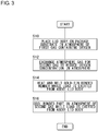
- Fig. 3 is a flowchart showing a method of manufacturing the optical semiconductor apparatus 10 according to the embodiment.
- the lid body 40 is placed on the package substrate 30 in which the optical semiconductor device 20 is housed in the atmosphere of the first gas containing oxygen (S10).
- the oxygen concentration in the first gas is 10 volume % or higher.
- the oxygen concentration is 20 volume % or higher.
- the first gas may be a dry air containing nitrogen (N 2 ) and oxygen.
- the gold-tin metal bonding member 56 is ensured to be sandwiched between the top surface 31 of the package substrate 30 and the inner surface of the lid body 40.
- the metal bonding member 56 is a preform of a frame shape associated with the frame-shaped first metal layer 51.
- the metal bonding member 56 may be attached to the first metal layer 51 of the package substrate 30 in advance.
- the metal bonding member 56 may be attached to the second metal layer 52 of the lid body 40.
- the atmosphere gas is exchanged for the second gas while the lid body 40 is being placed on the package substrate 30 so as to reduce the oxygen concentration in the atmosphere (S12).
- the second gas is an inert gas that does not substantially contain oxygen.
- the second gas is a pure nitrogen gas.
- the oxygen concentration in the second gas is 0.01 volume % or lower.
- the oxygen concentration is 0.005 volume % or lower.
- the gold-tin bonding member 56 is heated and melted while a load is exerted from the above the lid body 40 (S14). This forms gold-tin eutectic bonding between the first metal layer 51 of the package substrate 30 and the second metal layer 52 of the lid body 40.
- the bonding member when the oxygen concentration inside the package substrate 30 is 1 volume % or higher, and, preferably, 3 volume % or higher, and when the oxygen concentration outside the package substrate 30 is 0.1 volume % or lower, and, preferably, 0.04 volume % or lower.
- the metal bonding part 53 is cooled in the atmosphere of the second gas while the load is being exerted from above the lid body 40 (S16).
- the heated and melted metal bonding member 56 in the atmosphere of the second gas that does not substantially contain oxygen until the metal bonding member 56 is cooled and solidified, oxidation of the metal bonding part 53 is prevented and a highly reliable eutectic bonding part is formed. This completes the optical semiconductor apparatus 10 shown in Fig. 1 .
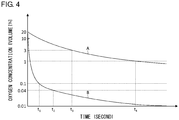
- Fig. 4 is a graph schematically showing variation in the oxygen concentration inside and outside the package when the atmosphere gas is exchanged.
- a curve A in the graph shows variation in the oxygen concentration inside the package substrate 30, and a curve B in the graph shows variation in the oxygen concentration outside the package substrate 30.
- the oxygen concentration in the first gas is 20 volume %
- the oxygen concentration in the second gas is 0.005 volume %.
- the graph shows time elapsed since the exchange for the second gas is started, and the oxygen concentration in the vertical axis [volume %] is defined on a logarithmic scale.
- the curve B the oxygen concentration outside the package substrate 30 drops rapidly due to the introduction of the second gas that does not substantially contain oxygen.
- the oxygen concentration in the atmosphere outside the package is 0.1 volume % at time t 1 and 0.04 volume % at time t 2 .
- the oxygen concentration inside the package substrate 30 drops more slowly than the oxygen concentration outside the package substrate 30.
- the oxygen concentration inside the package becomes 3 volume % at time t 3 after time t 2 and becomes 1 volume % at time t 4 .
- the graph shows that gold-tin bonding can be performed in a condition in which the oxygen concentration outside the package is 0.1 volume % or lower and the oxygen concentration inside the package is 1 volume % or higher, by heating and melting the metal bonding member 56 between time t 1 and t 4 after the exchange for the second gas is started. Further by heating and melting the metal bonding member 56 between time t 2 and t 3 , gold-tin bonding can be performed in a suitable condition in which the oxygen concentration outside the package is 0.04 volume % or lower and the oxygen concentration inside the package is 3 volume % or higher. Variation in the oxygen concentration inside and outside the package depends on the volume of the chamber 62, the flow rate of the second gas, the level of temporary sealing between the package substrate 30 and the lid body 40, etc.
- time t 1 is after 1 - 5 seconds
- time t 2 is after 5 - 10 seconds
- time t 3 is after 10 - 15 seconds
- time t 4 is after 20 - 30 seconds.
- the metal bonding part 53 is formed in a suitable oxygen concentration condition by heating and melting the metal bonding member 56 after a wait of about 5 - 15 seconds (e.g., 10 seconds) since the exchange for the second gas is started.
- oxidation of at least the metal bonding member 56 located at the outer circumference of the package is prevented when the metal bonding member 56 is heated and melted. Accordingly, the quality of bonding at the outer circumference of the package is improved. This improves the reliability of the sealing structure 50. Further, oxygen remains inside the package in a certain amount of larger so that degradation of the semiconductor stack structure 22 due to a low oxygen concentration is suitably prevented. This extends the life of the optical semiconductor device 20 and improves the reliability of the optical semiconductor apparatus 10.
- optical semiconductor device in the package of the optical semiconductor apparatus.
- electronic components other than the optical semiconductor device may be built in the package to provide additional functions.
- a Zener diode for protecting the optical semiconductor device from an electric surge may be built in the housing.
- a fluorescent body for converting the wavelength of the light output by the optical semiconductor device may be built in.
- an optical device for controlling the orientation of the light emitted by the optical semiconductor device may be built in.
- the embodiment and the variation described above have shown the optical semiconductor apparatus in which a light emitting device is sealed in the package.
- the sealing structure described above may be used to seal a light receiving device.
- the package structure described above may be used to seal a light receiving device for receiving deep ultraviolet light.
- the package described above may be used to seal an optical semiconductor device.
- the ceramic material used may be a low temperature co-fired ceramic (LTCC) multilayer substrate containing silica (SiO 2 ), calcium oxide (CaO), boron oxide (B 2 O 3 ), etc.
- the electrode or the metal layer may be formed on the substrate by using a metal material having a relatively low melting point such as copper (Cu) and silver (Ag) in place of a high melting point material such as tungsten and molybdenum and forming a multilayer film of Ni/Au on the base member.
- the reliability of the optical semiconductor apparatus is improved.
Landscapes
- Physics & Mathematics (AREA)
- Condensed Matter Physics & Semiconductors (AREA)
- General Physics & Mathematics (AREA)
- Electromagnetism (AREA)
- Optics & Photonics (AREA)
- Led Device Packages (AREA)
- Semiconductor Lasers (AREA)
- Engineering & Computer Science (AREA)
- Microelectronics & Electronic Packaging (AREA)
Abstract
Description
- The present invention relates to optical semiconductor apparatuses, and, more particularly, to an optical semiconductor apparatus including an optical semiconductor device.
- Nowadays, semiconductor light emitting devices such as light emitting diodes and laser diodes that emit blue light have been in practical use. Development of light emitting devices that output light having a shorter wavelength, and, more particularly, deep ultraviolet light has been pursued. Deep ultraviolet light has sterilization capability. Semiconductor light emitting devices capable of outputting deep ultraviolet light have attracted attention as a mercury-free sterilization light source in medical and food processing fronts.
- A light emitting device is housed in a package to protect the device from an external environment. In the case of a nitride semiconductor capable of outputting deep ultraviolet light, it is known that degradation of the semiconductor layer is inhibited by sealing the semiconductor in an atmosphere gas containing oxygen. For example, the light emitting device is sealed in a gas containing oxygen (O2) and nitrogen (N2) (see, for example, patent document 1). There is also proposed a technology to seal a light emitting device for deep ultraviolet light with a high reliability by using eutectic bonding of gold-tin (AuSn) (see, for example, patent document 2).
-
- [patent document 1]
JP2007-67373 - [patent document 2]
JP2015-18873 - When gold-tin is used as a sealing member, and when the atmosphere gas for a sealing step contains oxygen, the gold-sin is oxidized when the gold-tin alloy is heated and melted. As a result, reliable sealing might be prevented. Meanwhile, if the sealing gas does not contain oxygen, the optical semiconductor device is likely to be degraded and the reliability of the optical semiconductor apparatus is lowered.
- In this background, one illustrative purpose of the present invention is to provide a technology for increasing the reliability of an optical semiconductor apparatus.
- A method of manufacturing an optical semiconductor apparatus according to an embodiment of the present invention includes: placing a light transmissive lid body on a package substrate adapted to house an optical semiconductor device in an atmosphere of a first gas containing oxygen (O2), sandwiching a bonding member containing gold-tin (AuSn); exchanging an atmosphere gas for a second gas so as to reduce an oxygen concentration in the atmosphere while a load is exerted from above the lid body placed on the package substrate for temporary sealing; and heating and melting the bonding member after an exchange for the second gas is started so as to bond the package substrate and the lid body.
- According to this embodiment, the sealed gas in the package can contain oxygen by placing the lid body in an atmosphere of the first gas containing oxygen. By lowering the oxygen concentration in the atmosphere while the load is exerted on the lid body for temporary sealing, oxygen is inhibited from leaking outside the package and is allowed to remain in the package, and, at the same time, the gold-tin bonding member is heated and melted in a condition of a low oxygen concentration in the atmosphere so as to form eutectic bonding suitably. Thus, according to the embodiment, the optical semiconductor device is prevented from being degraded by sealing oxygen, and, at the same time, oxidation of the gold-tin bonding member is prevented. Accordingly, a highly reliable optical semiconductor apparatus can be manufactured.
- The method may further include: cooling a bonding part while maintaining the load exerted from above the lid body bonded on the package substrate in an atmosphere of a second gas.
- An oxygen (O2) content percentage in the first gas may be 10 volume % or higher, and an oxygen (O2) content percentage in the second gas may be 0.01 volume % or lower.
- The bonding member may start to be heated and melted before an oxygen concentration inside the package substrate drops to 1 volume % or lower.
- The bonding member may start to be heated and melted after an oxygen concentration outside the package substrate drops to 0.1 volume % or lower.
- According to the present invention, the reliability of the optical semiconductor apparatus is increased.
-
-
Fig. 1 is a cross sectional view schematically showing an optical semiconductor apparatus according to the embodiment; -
Fig. 2 schematically shows a process of manufacturing the optical semiconductor apparatus; -
Fig. 3 is a flowchart showing a method of manufacturing the optical semiconductor apparatus; and -
Fig. 4 is a graph schematically showing variation in the oxygen concentration inside and outside the package when the atmosphere gas is exchanged. - A description will be given of an embodiment of the present invention with reference to the drawings. Like numerals are used in the description to denote like elements and duplicate descriptions are omitted as appropriate. To facilitate the understanding, the relative dimensions of the constituting elements in the drawings do not necessarily mirror the relative dimensions in the actual apparatus.
-
Fig. 1 is a cross sectional view schematically showing anoptical semiconductor apparatus 10 according to the embodiment. Theoptical semiconductor apparatus 10 includes anoptical semiconductor device 20, apackage substrate 30, alid body 40, and asealing structure 50. - The
optical semiconductor device 20 is a light emitting diode (LED) chip configured to emit "deep ultraviolet light" having a central wavelength λ of about 360 nm or lower. To output deep ultraviolet light having such a wavelength, theoptical semiconductor device 20 is made of an aluminum gallium nitride (AlGaN) based semiconductor material having a band gap of about 3.4 eV or larger. The embodiment particularly discusses a case of emitting deep ultraviolet light having a central wavelength λ of about 240 nm - 350 nm. - The
optical semiconductor device 20 includes asemiconductor stack structure 22, alight emission surface 24, afirst device electrode 26, and asecond device electrode 27. - The
semiconductor stack structure 22 includes a template layer, an n-type clad layer, an active layer, a p-type clad layer, etc. built on a substrate that embodies thelight emission surface 24. When theoptical semiconductor device 20 is configured to output deep ultraviolet light, a sapphire (Al2O3) substrate is used as the substrate embodying thelight emission surface 24, and an aluminum nitride (AlN) layer is used as the template layer of thesemiconductor stack structure 22. The clad layer and the active layer of thesemiconductor stack structure 22 are made of an AlGaN-based semiconductor material. - The
first device electrode 26 and thesecond device electrode 27 are electrodes for supplying carriers to the active layer of thesemiconductor stack structure 22 and are an anode electrode and a cathode electrode, respectively. Thefirst device electrode 26 and thesecond device electrode 27 are provided opposite to thelight emission surface 24. Thefirst device electrode 26 is attached to a firstinner electrode 36 of thepackage substrate 30, and thesecond device electrode 27 is attached to a secondinner electrode 37 of thepackage substrate 30. - The
package substrate 30 is a rectangular member having atop surface 31 and abottom surface 32. Thepackage substrate 30 is a ceramic substrate that contains alumina (Al2O3), aluminum nitride (AlN), etc. and is a so-called high temperature co-fired ceramic (HTCC) multilayer substrate. - A
recess 34 for housing theoptical semiconductor device 20 is provided on thetop surface 31 of thepackage substrate 30. The firstinner electrode 36 and the secondinner electrode 37 to which theoptical semiconductor device 20 is attached are provided on the bottom surface of therecess 34. On thebottom surface 32 of thepackage substrate 30 are provided a firstouter electrode 38 and a secondouter electrode 39 for mounting theoptical semiconductor apparatus 10 on, for example, an external substrate. - The
lid body 40 is a plate-like protective member provided to cover the opening of therecess 34. Thelid body 40 is made of a material that transmits ultraviolet light emitted by theoptical semiconductor device 20. For example, glass, quartz, crystal, sapphire, etc. may be used. Thelid body 40 is preferably made of a material having a high deep ultraviolet transmittance and highly heat resistant and airtight. Quartz glass is a material having such a property and is desirably used in thelid body 40. The ultraviolet light emitted by theoptical semiconductor device 20 is output via thelid body 40 from anouter surface 43 of thelid body 40 to a space outside the package. - The
sealing structure 50 includes afirst metal layer 51, asecond metal layer 52, and ametal bonding part 53. - The
first metal layer 51 is provided on thetop surface 31 of thepackage substrate 30 in a shape of a frame. Thefirst metal layer 51 has a rectangular frame shape associated with therectangular package substrate 30. The four corners of thefirst metal layer 51 may be rounded. Thefirst metal layer 51 is formed by, for example, metalizing a ceramic substrate. Thefirst metal layer 51 is formed by plating a base member containing tungsten (W) or molybdenum (Mo) with nickel (Ni), gold (Au), etc. and has a stack structure of W/Ni/Au. Thefirst metal layer 51 is bonded to themetal bonding part 53. - The
second metal layer 52 is provided on aninner surface 44 of thelid body 40 in a shape of a frame. Thesecond metal layer 52 has a rectangular frame shape associated with therectangular lid body 40. The four corners of thesecond metal layer 52 may be rounded. Thesecond metal layer 52 is formed by a method such as vacuum deposition and sputtering. Thesecond metal layer 52 is a multilayer film in which titanium (Ti), platinum (Pt), and gold (Au) are built on theinner surface 44 of thelid body 40 in the stated order. Chromium (Cr) may be used in place of titanium, and copper (Cu) and nickel (Ni) may be used in place of platinum (Pt). Thesecond metal layer 52 is bonded to themetal bonding part 53. - The
metal bonding part 53 is provided between thefirst metal layer 51 and thesecond metal layer 52 and bonds and seals thepackage substrate 30 and thelid body 40 at the outer circumference of the package. Themetal bonding part 53 is configured to fill a space between thefirst metal layer 51 and thesecond metal layer 52. Themetal bonding part 53 is made of a metal material having a low melting point and contains, for example, gold-tin (AuSn). Themetal bonding part 53 spreads between thefirst metal layer 51 and thesecond metal layer 52 when melted to form eutectic bonding. It is preferable that themetal bonding part 53 is made of gold-tin containing tin (Sn) in an amount of 20 weight % - 24 weight % to ensure high sealing reliability and a melting temperature of 300°C or lower. - A gas containing oxygen (O2) is sealed inside the package housing the
optical semiconductor device 20. By containing oxygen in the sealed gas, degradation of theoptical semiconductor device 20 is prevented, and the life of theoptical semiconductor apparatus 10 is extended as compared to the case of sealing a gas that does not substantially contain oxygen. A mixture of an inert gas such as nitrogen (N2) with a certain amount of oxygen may be used as the sealed gas. The oxygen concentration in the sealed gas may be 1 volume % or higher, and, preferably, 3 volume % or higher. - When a gold-tin bonding member is heated and melted to form the
metal bonding part 53 and when oxygen is contained in the atmosphere, the gold-tin alloy might be inhibited from being melted due to oxidation so that the reliability of sealing might be lowered. Generally, the oxygen concentration needs to be 0.1 volume % or lower, and, preferably, 0.04 volume percent or lower to prevent oxidation of gold-tin. Meanwhile, the oxygen concentration in the sealed gas is preferably 1 volume % or higher. If the gold-tin bonding member is heated and melted in an atmosphere of such a sealed gas, gold-tin will be oxidized. This is addressed in this embodiment by performing a step of gold-tin bonding in an environment in which a certain amount of oxygen or larger is contained in the package of theoptical semiconductor apparatus 10 but oxygen is not substantially contained outside the package of theoptical semiconductor apparatus 10. A description will now be given of a method of manufacturing theoptical semiconductor apparatus 10 for performing such a bonding step. -
Fig. 2 schematically shows a process of manufacturing theoptical semiconductor apparatus 10 and shows anexemplary manufacturing apparatus 60 used to seal theoptical semiconductor apparatus 10. Themanufacturing apparatus 60 includes achamber 62, a table 64, a heating andcooling mechanism 66, a lidbody transportation unit 68, a firstgas supply port 72, a secondgas supply port 74, and agas discharge port 76. - The
chamber 62 is a container in which the step of sealing theoptical semiconductor apparatus 10 is performed. Thechamber 62 is provided with the firstgas supply port 72, the secondgas supply port 74, and thegas discharge port 76. The firstgas supply port 72 is connected to a firstgas supply unit 82 and introduces a first gas with an oxygen concentration of 10 volume % or higher into thechamber 62. The secondgas supply port 74 is connected to a secondgas supply unit 84 and introduces a second gas with an oxygen concentration of 0.01 volume % or lower into thechamber 62. Thegas discharge port 76 is opened when the atmosphere gas in thechamber 62 is exchanged and discharges the gas subject to exchange outside thechamber 62. - The table 64 is provided in the
chamber 62, and thepackage substrate 30 subject to sealing is placed on the table 64. The heating andcooling mechanism 66 is provided on the table 64. The heating andcooling mechanism 66 includes a heater for heating thepackage substrate 30 and an air cooling mechanism or a water cooling mechanism for cooling thepackage substrate 30, thereby enabling heating and cooling of thepackage substrate 30. The heating andcooling mechanism 66 may only include a heating function, and thepackage substrate 30 may be cooled by natural heat dissipation. - The lid
body transportation unit 68 is provided above the table 64. The lidbody transportation unit 68 is configured to transport thelid body 40 above thepackage substrate 30 to place thelid body 40 on thepackage substrate 30. The lidbody transportation unit 68 exerts a load on thelid body 40 placed on thepackage substrate 30 temporarily seal a space between thepackage substrate 30 and thelid body 40. Ametal bonding member 56 may be temporarily secured to one of thepackage substrate 30 and thelid body 40 in advance. Alternatively, themetal bonding member 56 may be placed on thepackage substrate 30 by means of the lidbody transportation unit 68 before thelid body 40 is transported. -
Fig. 3 is a flowchart showing a method of manufacturing theoptical semiconductor apparatus 10 according to the embodiment. First, thelid body 40 is placed on thepackage substrate 30 in which theoptical semiconductor device 20 is housed in the atmosphere of the first gas containing oxygen (S10). The oxygen concentration in the first gas is 10 volume % or higher. Preferably, the oxygen concentration is 20 volume % or higher. The first gas may be a dry air containing nitrogen (N2) and oxygen. In this process, the gold-tinmetal bonding member 56 is ensured to be sandwiched between thetop surface 31 of thepackage substrate 30 and the inner surface of thelid body 40. For example, themetal bonding member 56 is a preform of a frame shape associated with the frame-shapedfirst metal layer 51. Themetal bonding member 56 may be attached to thefirst metal layer 51 of thepackage substrate 30 in advance. Alternatively, themetal bonding member 56 may be attached to thesecond metal layer 52 of thelid body 40. - Subsequently, the atmosphere gas is exchanged for the second gas while the
lid body 40 is being placed on thepackage substrate 30 so as to reduce the oxygen concentration in the atmosphere (S12). The second gas is an inert gas that does not substantially contain oxygen. For example, the second gas is a pure nitrogen gas. The oxygen concentration in the second gas is 0.01 volume % or lower. Preferably, the oxygen concentration is 0.005 volume % or lower. By exchanging the atmosphere gas for the second gas that does not substantially contain oxygen, the oxygen concentration in the atmosphere outside thepackage substrate 30 is reduced. In this process, it is preferable to temporarily seal a space between thepackage substrate 30 and thelid body 40 by exerting a load from theabove lid body 40 to inhibit the oxygen inside thepackage substrate 30 from leaking outside to lower the oxygen concentration in thepackage substrate 30. Temporary sealing does not completely seal the package but increases the airtightness inside thepackage substrate 30 by reducing the gap between thepackage substrate 30 and thelid body 40. - Subsequently, after the step of exchanging the atmosphere gas for the second gas is started, the gold-
tin bonding member 56 is heated and melted while a load is exerted from the above the lid body 40 (S14). This forms gold-tin eutectic bonding between thefirst metal layer 51 of thepackage substrate 30 and thesecond metal layer 52 of thelid body 40. In regard to the timing of heating the gold-tin bonding member, it is desirable to heat the gold-tin bonding member in parallel with the step of exchanging for the second gas instead of waiting until the atmosphere gas is completed exchanged for the second gas. More specifically, it is preferable to heat and melt the bonding member when the oxygen concentration inside thepackage substrate 30 is 1 volume % or higher, and, preferably, 3 volume % or higher, and when the oxygen concentration outside thepackage substrate 30 is 0.1 volume % or lower, and, preferably, 0.04 volume % or lower. By performing heating and melting in the condition as described above, it is ensured that oxygen of 1 volume % or higher is contained inside thepackage substrate 30 and, at the same time, gold-tin is heated and melted in an atmosphere of an oxygen concentration of 0.1 volume % or lower. - Subsequently, the
metal bonding part 53 is cooled in the atmosphere of the second gas while the load is being exerted from above the lid body 40 (S16). By placing the heated and meltedmetal bonding member 56 in the atmosphere of the second gas that does not substantially contain oxygen until themetal bonding member 56 is cooled and solidified, oxidation of themetal bonding part 53 is prevented and a highly reliable eutectic bonding part is formed. This completes theoptical semiconductor apparatus 10 shown inFig. 1 . -
Fig. 4 is a graph schematically showing variation in the oxygen concentration inside and outside the package when the atmosphere gas is exchanged. A curve A in the graph shows variation in the oxygen concentration inside thepackage substrate 30, and a curve B in the graph shows variation in the oxygen concentration outside thepackage substrate 30. In the example shown in the graph, the oxygen concentration in the first gas is 20 volume %, and the oxygen concentration in the second gas is 0.005 volume %. The graph shows time elapsed since the exchange for the second gas is started, and the oxygen concentration in the vertical axis [volume %] is defined on a logarithmic scale. As indicated by the curve B, the oxygen concentration outside thepackage substrate 30 drops rapidly due to the introduction of the second gas that does not substantially contain oxygen. For example, the oxygen concentration in the atmosphere outside the package is 0.1 volume % at time t1 and 0.04 volume % at time t2. Meanwhile, the oxygen concentration inside thepackage substrate 30 drops more slowly than the oxygen concentration outside thepackage substrate 30. For example, the oxygen concentration inside the package becomes 3 volume % at time t3 after time t2 and becomes 1 volume % at time t4. - The graph shows that gold-tin bonding can be performed in a condition in which the oxygen concentration outside the package is 0.1 volume % or lower and the oxygen concentration inside the package is 1 volume % or higher, by heating and melting the
metal bonding member 56 between time t1 and t4 after the exchange for the second gas is started. Further by heating and melting themetal bonding member 56 between time t2 and t3, gold-tin bonding can be performed in a suitable condition in which the oxygen concentration outside the package is 0.04 volume % or lower and the oxygen concentration inside the package is 3 volume % or higher. Variation in the oxygen concentration inside and outside the package depends on the volume of thechamber 62, the flow rate of the second gas, the level of temporary sealing between thepackage substrate 30 and thelid body 40, etc. In one embodiment, time t1 is after 1 - 5 seconds, time t2 is after 5 - 10 seconds, time t3 is after 10 - 15 seconds, and time t4 is after 20 - 30 seconds. Accordingly, themetal bonding part 53 is formed in a suitable oxygen concentration condition by heating and melting themetal bonding member 56 after a wait of about 5 - 15 seconds (e.g., 10 seconds) since the exchange for the second gas is started. - According to the embodiment, oxidation of at least the
metal bonding member 56 located at the outer circumference of the package is prevented when themetal bonding member 56 is heated and melted. Accordingly, the quality of bonding at the outer circumference of the package is improved. This improves the reliability of the sealingstructure 50. Further, oxygen remains inside the package in a certain amount of larger so that degradation of thesemiconductor stack structure 22 due to a low oxygen concentration is suitably prevented. This extends the life of theoptical semiconductor device 20 and improves the reliability of theoptical semiconductor apparatus 10. - Described above is an explanation based on an exemplary embodiment. The embodiment is intended to be illustrative only and it will be understood by those skilled in the art that various design changes are possible and various modifications are possible and that such modifications are also within the scope of the present invention.
- The embodiment and the variation described above have shown the case of including only the optical semiconductor device in the package of the optical semiconductor apparatus. In a further variation, electronic components other than the optical semiconductor device may be built in the package to provide additional functions. For example, a Zener diode for protecting the optical semiconductor device from an electric surge may be built in the housing. A fluorescent body for converting the wavelength of the light output by the optical semiconductor device may be built in. Still alternatively, an optical device for controlling the orientation of the light emitted by the optical semiconductor device may be built in.
- The embodiment and the variation described above have shown the optical semiconductor apparatus in which a light emitting device is sealed in the package. In a further variation, the sealing structure described above may be used to seal a light receiving device. For example, the package structure described above may be used to seal a light receiving device for receiving deep ultraviolet light. In essence, the package described above may be used to seal an optical semiconductor device.
- The embodiment and the variation described above have shown the case of using a high temperature co-fired ceramic (HTCC) multilayer substrate as a material of the substrate. In a further variation, the ceramic material used may be a low temperature co-fired ceramic (LTCC) multilayer substrate containing silica (SiO2), calcium oxide (CaO), boron oxide (B2O3), etc. In this case, the electrode or the metal layer may be formed on the substrate by using a metal material having a relatively low melting point such as copper (Cu) and silver (Ag) in place of a high melting point material such as tungsten and molybdenum and forming a multilayer film of Ni/Au on the base member.
- 10 ... optical semiconductor apparatus, 20 ... optical semiconductor device, 30 ... package substrate, 40 ... lid body, 53 ... metal bonding part, 56 ... metal bonding member
- According to the present invention, the reliability of the optical semiconductor apparatus is improved.
Claims (5)
- A method of manufacturing an optical semiconductor apparatus comprising:placing a light transmissive lid body on a package substrate adapted to house an optical semiconductor device in an atmosphere of a first gas containing oxygen (O2), sandwiching a bonding member containing gold-tin (AuSn);exchanging an atmosphere gas for a second gas so as to reduce an oxygen concentration in the atmosphere while a load is exerted from above the lid body placed on the package substrate for temporary sealing; andheating and melting the bonding member after an exchange for the second gas is started so as to bond the package substrate and the lid body.
- The method of manufacturing an optical semiconductor apparatus according to claim 1, further comprising:
cooling a bonding part while maintaining the load exerted from above the lid body bonded on the package substrate in an atmosphere of a second gas. - The method of manufacturing an optical semiconductor apparatus according to claim 1 or 2, wherein
an oxygen (O2) content percentage in the first gas is 10 volume % or higher, and an oxygen (O2) content percentage in the second gas is 0.01 volume % or lower. - The method of manufacturing an optical semiconductor apparatus according to one of claims 1 through 3, wherein
the bonding member starts to be heated and melted before an oxygen concentration inside the package substrate drops to 1 volume % or lower. - The method of manufacturing an optical semiconductor apparatus according to one of claims 1 through 4, wherein
the bonding member starts to be heated and melted after an oxygen concentration outside the package substrate drops to 0.1 volume % or lower.
Applications Claiming Priority (2)
| Application Number | Priority Date | Filing Date | Title |
|---|---|---|---|
| JP2016237608A JP6339652B1 (en) | 2016-12-07 | 2016-12-07 | Manufacturing method of optical semiconductor device |
| PCT/JP2017/040816 WO2018105327A1 (en) | 2016-12-07 | 2017-11-13 | Production method for optical semiconductor device |
Publications (3)
| Publication Number | Publication Date |
|---|---|
| EP3457445A1 true EP3457445A1 (en) | 2019-03-20 |
| EP3457445A4 EP3457445A4 (en) | 2020-01-01 |
| EP3457445B1 EP3457445B1 (en) | 2021-03-17 |
Family
ID=62487274
Family Applications (1)
| Application Number | Title | Priority Date | Filing Date |
|---|---|---|---|
| EP17877831.2A Active EP3457445B1 (en) | 2016-12-07 | 2017-11-13 | Production method for optical semiconductor device |
Country Status (5)
| Country | Link |
|---|---|
| US (1) | US10439100B2 (en) |
| EP (1) | EP3457445B1 (en) |
| JP (1) | JP6339652B1 (en) |
| CN (1) | CN109075231B (en) |
| WO (1) | WO2018105327A1 (en) |
Families Citing this family (13)
| Publication number | Priority date | Publication date | Assignee | Title |
|---|---|---|---|---|
| DE102017125140B4 (en) * | 2017-10-26 | 2021-06-10 | Infineon Technologies Ag | Method for producing a hermetically sealed housing with a semiconductor component |
| JP7174242B2 (en) * | 2018-06-15 | 2022-11-17 | 日亜化学工業株式会社 | Semiconductor device manufacturing method |
| US10811581B2 (en) * | 2018-06-15 | 2020-10-20 | Nichia Corporation | Method of manufacturing semiconductor device |
| JP7138026B2 (en) * | 2018-11-28 | 2022-09-15 | 京セラ株式会社 | Optical device lid and method for manufacturing optical device lid |
| CN113646908A (en) * | 2019-07-25 | 2021-11-12 | 株式会社大真空 | Cover member of light-emitting device, method of manufacturing the cover member, and light-emitting device |
| WO2021014925A1 (en) * | 2019-07-25 | 2021-01-28 | 株式会社大真空 | Lid material for light-emitting device and method for manufacturing lid material |
| JP2021034502A (en) * | 2019-08-22 | 2021-03-01 | スタンレー電気株式会社 | Light-emitting device and manufacturing method thereof |
| JP7091303B2 (en) | 2019-09-27 | 2022-06-27 | Dowaエレクトロニクス株式会社 | Manufacturing method of optical semiconductor device and optical semiconductor device |
| JP7500317B2 (en) | 2020-07-22 | 2024-06-17 | スタンレー電気株式会社 | Semiconductor light emitting device |
| JP7554647B2 (en) * | 2020-11-24 | 2024-09-20 | スタンレー電気株式会社 | Semiconductor light emitting device and its manufacturing method |
| CN115764537B (en) * | 2021-06-22 | 2026-05-08 | 青岛海信激光显示股份有限公司 | laser |
| CN113451481B (en) * | 2021-06-28 | 2022-09-23 | 江西新正耀科技有限公司 | A kind of manufacturing method of deep ultraviolet light emitting element |
| WO2025070266A1 (en) * | 2023-09-26 | 2025-04-03 | 京セラ株式会社 | Light-emitting device |
Family Cites Families (16)
| Publication number | Priority date | Publication date | Assignee | Title |
|---|---|---|---|---|
| JPH0697645A (en) * | 1992-01-20 | 1994-04-08 | Tokyo Gas Co Ltd | Method and apparatus for reducing oxygen concentration in reflow soldering furnace |
| JPH11121920A (en) * | 1997-10-13 | 1999-04-30 | Nippon Telegr & Teleph Corp <Ntt> | Solder reflow method and device |
| DE102005029246B4 (en) * | 2005-03-31 | 2023-06-22 | OSRAM Opto Semiconductors Gesellschaft mit beschränkter Haftung | Semiconductor chip with a solder layer sequence and method for soldering a semiconductor chip |
| JP4964512B2 (en) * | 2005-08-02 | 2012-07-04 | シャープ株式会社 | Nitride semiconductor light emitting device |
| JP2007201411A (en) * | 2005-12-27 | 2007-08-09 | Sanyo Electric Co Ltd | Semiconductor laser device and manufacturing method thereof |
| US7667324B2 (en) * | 2006-10-31 | 2010-02-23 | Avago Technologies Fiber Ip (Singapore) Pte. Ltd. | Systems, devices, components and methods for hermetically sealing electronic modules and packages |
| US8525323B2 (en) * | 2008-07-25 | 2013-09-03 | Nec Corporation | Encapsulating package, printed circuit board, electronic device and method for manufacturing encapsulating package |
| JP2013042079A (en) * | 2011-08-19 | 2013-02-28 | Sharp Corp | Semiconductor light emitting device |
| DE102012200327B4 (en) * | 2012-01-11 | 2022-01-05 | Osram Gmbh | Optoelectronic component |
| US9240524B2 (en) * | 2012-03-05 | 2016-01-19 | Seoul Viosys Co., Ltd. | Light-emitting device and method of manufacturing the same |
| JP2014175565A (en) * | 2013-03-12 | 2014-09-22 | Ushio Inc | Semiconductor laser device |
| CN103137833A (en) * | 2013-03-15 | 2013-06-05 | 深圳市瑞丰光电子股份有限公司 | Method and structure of light emitting diode (LED) packaging |
| JP6128938B2 (en) * | 2013-04-26 | 2017-05-17 | 株式会社トクヤマ | Semiconductor light emitting device package |
| JP2014236202A (en) * | 2013-06-05 | 2014-12-15 | 旭硝子株式会社 | Light-emitting device |
| JP2015018873A (en) * | 2013-07-09 | 2015-01-29 | 日機装株式会社 | Semiconductor module |
| CN105280783A (en) * | 2015-11-18 | 2016-01-27 | 佛山市南海区联合广东新光源产业创新中心 | An ultraviolet led device |
-
2016
- 2016-12-07 JP JP2016237608A patent/JP6339652B1/en active Active
-
2017
- 2017-11-13 EP EP17877831.2A patent/EP3457445B1/en active Active
- 2017-11-13 CN CN201780023645.9A patent/CN109075231B/en active Active
- 2017-11-13 WO PCT/JP2017/040816 patent/WO2018105327A1/en not_active Ceased
-
2018
- 2018-11-20 US US16/196,997 patent/US10439100B2/en active Active
Also Published As
| Publication number | Publication date |
|---|---|
| EP3457445B1 (en) | 2021-03-17 |
| CN109075231B (en) | 2021-02-12 |
| EP3457445A4 (en) | 2020-01-01 |
| US10439100B2 (en) | 2019-10-08 |
| JP2018093137A (en) | 2018-06-14 |
| WO2018105327A1 (en) | 2018-06-14 |
| JP6339652B1 (en) | 2018-06-06 |
| CN109075231A (en) | 2018-12-21 |
| US20190088818A1 (en) | 2019-03-21 |
Similar Documents
| Publication | Publication Date | Title |
|---|---|---|
| US10439100B2 (en) | Method of manufacturing optical semiconductor apparatus | |
| US11222998B2 (en) | Optical semiconductor apparatus and method of manufacturing optical semiconductor apparatus | |
| US10840414B2 (en) | Optical semiconductor apparatus and method of manufacturing optical semiconductor apparatus | |
| US11217730B2 (en) | Optical semiconductor apparatus and method of manufacturing optical semiconductor apparatus | |
| US11942569B2 (en) | Methods and packages for enhancing reliability of ultraviolet light-emitting devices | |
| US20220293825A1 (en) | Method of manufacturing optical semiconductor device and optical semiconductor device | |
| CN113161467B (en) | Light emitting device and water sterilizing device | |
| WO2021033526A1 (en) | Light-emitting device and method for manufacturing same | |
| JP6932019B2 (en) | Light emitting device | |
| WO2022138844A1 (en) | Silica member and led device |
Legal Events
| Date | Code | Title | Description |
|---|---|---|---|
| STAA | Information on the status of an ep patent application or granted ep patent |
Free format text: STATUS: THE INTERNATIONAL PUBLICATION HAS BEEN MADE |
|
| PUAI | Public reference made under article 153(3) epc to a published international application that has entered the european phase |
Free format text: ORIGINAL CODE: 0009012 |
|
| STAA | Information on the status of an ep patent application or granted ep patent |
Free format text: STATUS: REQUEST FOR EXAMINATION WAS MADE |
|
| 17P | Request for examination filed |
Effective date: 20181210 |
|
| AK | Designated contracting states |
Kind code of ref document: A1 Designated state(s): AL AT BE BG CH CY CZ DE DK EE ES FI FR GB GR HR HU IE IS IT LI LT LU LV MC MK MT NL NO PL PT RO RS SE SI SK SM TR |
|
| AX | Request for extension of the european patent |
Extension state: BA ME |
|
| A4 | Supplementary search report drawn up and despatched |
Effective date: 20191203 |
|
| RIC1 | Information provided on ipc code assigned before grant |
Ipc: H01L 31/0203 20140101ALI20191127BHEP Ipc: H01L 33/48 20100101AFI20191127BHEP Ipc: H01L 23/02 20060101ALI20191127BHEP Ipc: H01L 33/56 20100101ALI20191127BHEP Ipc: H01S 5/022 20060101ALI20191127BHEP Ipc: H01L 33/32 20100101ALN20191127BHEP |
|
| DAV | Request for validation of the european patent (deleted) | ||
| DAX | Request for extension of the european patent (deleted) | ||
| GRAP | Despatch of communication of intention to grant a patent |
Free format text: ORIGINAL CODE: EPIDOSNIGR1 |
|
| STAA | Information on the status of an ep patent application or granted ep patent |
Free format text: STATUS: GRANT OF PATENT IS INTENDED |
|
| RIC1 | Information provided on ipc code assigned before grant |
Ipc: H01L 33/56 20100101ALI20200928BHEP Ipc: H01L 23/02 20060101ALI20200928BHEP Ipc: H01L 33/48 20100101AFI20200928BHEP Ipc: H01L 31/0203 20140101ALI20200928BHEP Ipc: H01L 33/32 20100101ALN20200928BHEP Ipc: H01S 5/022 20060101ALI20200928BHEP |
|
| INTG | Intention to grant announced |
Effective date: 20201022 |
|
| GRAS | Grant fee paid |
Free format text: ORIGINAL CODE: EPIDOSNIGR3 |
|
| GRAA | (expected) grant |
Free format text: ORIGINAL CODE: 0009210 |
|
| STAA | Information on the status of an ep patent application or granted ep patent |
Free format text: STATUS: THE PATENT HAS BEEN GRANTED |
|
| AK | Designated contracting states |
Kind code of ref document: B1 Designated state(s): AL AT BE BG CH CY CZ DE DK EE ES FI FR GB GR HR HU IE IS IT LI LT LU LV MC MK MT NL NO PL PT RO RS SE SI SK SM TR |
|
| REG | Reference to a national code |
Ref country code: GB Ref legal event code: FG4D |
|
| REG | Reference to a national code |
Ref country code: CH Ref legal event code: EP |
|
| REG | Reference to a national code |
Ref country code: DE Ref legal event code: R096 Ref document number: 602017035006 Country of ref document: DE |
|
| REG | Reference to a national code |
Ref country code: IE Ref legal event code: FG4D |
|
| REG | Reference to a national code |
Ref country code: AT Ref legal event code: REF Ref document number: 1373046 Country of ref document: AT Kind code of ref document: T Effective date: 20210415 |
|
| REG | Reference to a national code |
Ref country code: LT Ref legal event code: MG9D |
|
| PG25 | Lapsed in a contracting state [announced via postgrant information from national office to epo] |
Ref country code: NO Free format text: LAPSE BECAUSE OF FAILURE TO SUBMIT A TRANSLATION OF THE DESCRIPTION OR TO PAY THE FEE WITHIN THE PRESCRIBED TIME-LIMIT Effective date: 20210617 Ref country code: HR Free format text: LAPSE BECAUSE OF FAILURE TO SUBMIT A TRANSLATION OF THE DESCRIPTION OR TO PAY THE FEE WITHIN THE PRESCRIBED TIME-LIMIT Effective date: 20210317 Ref country code: GR Free format text: LAPSE BECAUSE OF FAILURE TO SUBMIT A TRANSLATION OF THE DESCRIPTION OR TO PAY THE FEE WITHIN THE PRESCRIBED TIME-LIMIT Effective date: 20210618 Ref country code: FI Free format text: LAPSE BECAUSE OF FAILURE TO SUBMIT A TRANSLATION OF THE DESCRIPTION OR TO PAY THE FEE WITHIN THE PRESCRIBED TIME-LIMIT Effective date: 20210317 Ref country code: BG Free format text: LAPSE BECAUSE OF FAILURE TO SUBMIT A TRANSLATION OF THE DESCRIPTION OR TO PAY THE FEE WITHIN THE PRESCRIBED TIME-LIMIT Effective date: 20210617 |
|
| REG | Reference to a national code |
Ref country code: AT Ref legal event code: MK05 Ref document number: 1373046 Country of ref document: AT Kind code of ref document: T Effective date: 20210317 |
|
| REG | Reference to a national code |
Ref country code: NL Ref legal event code: MP Effective date: 20210317 |
|
| PG25 | Lapsed in a contracting state [announced via postgrant information from national office to epo] |
Ref country code: LV Free format text: LAPSE BECAUSE OF FAILURE TO SUBMIT A TRANSLATION OF THE DESCRIPTION OR TO PAY THE FEE WITHIN THE PRESCRIBED TIME-LIMIT Effective date: 20210317 Ref country code: RS Free format text: LAPSE BECAUSE OF FAILURE TO SUBMIT A TRANSLATION OF THE DESCRIPTION OR TO PAY THE FEE WITHIN THE PRESCRIBED TIME-LIMIT Effective date: 20210317 Ref country code: SE Free format text: LAPSE BECAUSE OF FAILURE TO SUBMIT A TRANSLATION OF THE DESCRIPTION OR TO PAY THE FEE WITHIN THE PRESCRIBED TIME-LIMIT Effective date: 20210317 |
|
| PG25 | Lapsed in a contracting state [announced via postgrant information from national office to epo] |
Ref country code: NL Free format text: LAPSE BECAUSE OF FAILURE TO SUBMIT A TRANSLATION OF THE DESCRIPTION OR TO PAY THE FEE WITHIN THE PRESCRIBED TIME-LIMIT Effective date: 20210317 |
|
| PG25 | Lapsed in a contracting state [announced via postgrant information from national office to epo] |
Ref country code: EE Free format text: LAPSE BECAUSE OF FAILURE TO SUBMIT A TRANSLATION OF THE DESCRIPTION OR TO PAY THE FEE WITHIN THE PRESCRIBED TIME-LIMIT Effective date: 20210317 Ref country code: CZ Free format text: LAPSE BECAUSE OF FAILURE TO SUBMIT A TRANSLATION OF THE DESCRIPTION OR TO PAY THE FEE WITHIN THE PRESCRIBED TIME-LIMIT Effective date: 20210317 Ref country code: LT Free format text: LAPSE BECAUSE OF FAILURE TO SUBMIT A TRANSLATION OF THE DESCRIPTION OR TO PAY THE FEE WITHIN THE PRESCRIBED TIME-LIMIT Effective date: 20210317 Ref country code: SM Free format text: LAPSE BECAUSE OF FAILURE TO SUBMIT A TRANSLATION OF THE DESCRIPTION OR TO PAY THE FEE WITHIN THE PRESCRIBED TIME-LIMIT Effective date: 20210317 Ref country code: AT Free format text: LAPSE BECAUSE OF FAILURE TO SUBMIT A TRANSLATION OF THE DESCRIPTION OR TO PAY THE FEE WITHIN THE PRESCRIBED TIME-LIMIT Effective date: 20210317 |
|
| PG25 | Lapsed in a contracting state [announced via postgrant information from national office to epo] |
Ref country code: IS Free format text: LAPSE BECAUSE OF FAILURE TO SUBMIT A TRANSLATION OF THE DESCRIPTION OR TO PAY THE FEE WITHIN THE PRESCRIBED TIME-LIMIT Effective date: 20210717 Ref country code: PL Free format text: LAPSE BECAUSE OF FAILURE TO SUBMIT A TRANSLATION OF THE DESCRIPTION OR TO PAY THE FEE WITHIN THE PRESCRIBED TIME-LIMIT Effective date: 20210317 Ref country code: PT Free format text: LAPSE BECAUSE OF FAILURE TO SUBMIT A TRANSLATION OF THE DESCRIPTION OR TO PAY THE FEE WITHIN THE PRESCRIBED TIME-LIMIT Effective date: 20210719 Ref country code: SK Free format text: LAPSE BECAUSE OF FAILURE TO SUBMIT A TRANSLATION OF THE DESCRIPTION OR TO PAY THE FEE WITHIN THE PRESCRIBED TIME-LIMIT Effective date: 20210317 Ref country code: RO Free format text: LAPSE BECAUSE OF FAILURE TO SUBMIT A TRANSLATION OF THE DESCRIPTION OR TO PAY THE FEE WITHIN THE PRESCRIBED TIME-LIMIT Effective date: 20210317 |
|
| REG | Reference to a national code |
Ref country code: DE Ref legal event code: R097 Ref document number: 602017035006 Country of ref document: DE |
|
| PLBE | No opposition filed within time limit |
Free format text: ORIGINAL CODE: 0009261 |
|
| STAA | Information on the status of an ep patent application or granted ep patent |
Free format text: STATUS: NO OPPOSITION FILED WITHIN TIME LIMIT |
|
| PG25 | Lapsed in a contracting state [announced via postgrant information from national office to epo] |
Ref country code: AL Free format text: LAPSE BECAUSE OF FAILURE TO SUBMIT A TRANSLATION OF THE DESCRIPTION OR TO PAY THE FEE WITHIN THE PRESCRIBED TIME-LIMIT Effective date: 20210317 Ref country code: DK Free format text: LAPSE BECAUSE OF FAILURE TO SUBMIT A TRANSLATION OF THE DESCRIPTION OR TO PAY THE FEE WITHIN THE PRESCRIBED TIME-LIMIT Effective date: 20210317 Ref country code: ES Free format text: LAPSE BECAUSE OF FAILURE TO SUBMIT A TRANSLATION OF THE DESCRIPTION OR TO PAY THE FEE WITHIN THE PRESCRIBED TIME-LIMIT Effective date: 20210317 |
|
| 26N | No opposition filed |
Effective date: 20211220 |
|
| PG25 | Lapsed in a contracting state [announced via postgrant information from national office to epo] |
Ref country code: SI Free format text: LAPSE BECAUSE OF FAILURE TO SUBMIT A TRANSLATION OF THE DESCRIPTION OR TO PAY THE FEE WITHIN THE PRESCRIBED TIME-LIMIT Effective date: 20210317 |
|
| PG25 | Lapsed in a contracting state [announced via postgrant information from national office to epo] |
Ref country code: IT Free format text: LAPSE BECAUSE OF FAILURE TO SUBMIT A TRANSLATION OF THE DESCRIPTION OR TO PAY THE FEE WITHIN THE PRESCRIBED TIME-LIMIT Effective date: 20210317 |
|
| PG25 | Lapsed in a contracting state [announced via postgrant information from national office to epo] |
Ref country code: IS Free format text: LAPSE BECAUSE OF FAILURE TO SUBMIT A TRANSLATION OF THE DESCRIPTION OR TO PAY THE FEE WITHIN THE PRESCRIBED TIME-LIMIT Effective date: 20210717 |
|
| PG25 | Lapsed in a contracting state [announced via postgrant information from national office to epo] |
Ref country code: MC Free format text: LAPSE BECAUSE OF FAILURE TO SUBMIT A TRANSLATION OF THE DESCRIPTION OR TO PAY THE FEE WITHIN THE PRESCRIBED TIME-LIMIT Effective date: 20210317 |
|
| REG | Reference to a national code |
Ref country code: CH Ref legal event code: PL |
|
| GBPC | Gb: european patent ceased through non-payment of renewal fee |
Effective date: 20211113 |
|
| PG25 | Lapsed in a contracting state [announced via postgrant information from national office to epo] |
Ref country code: LU Free format text: LAPSE BECAUSE OF NON-PAYMENT OF DUE FEES Effective date: 20211113 Ref country code: BE Free format text: LAPSE BECAUSE OF NON-PAYMENT OF DUE FEES Effective date: 20211130 |
|
| REG | Reference to a national code |
Ref country code: BE Ref legal event code: MM Effective date: 20211130 |
|
| PG25 | Lapsed in a contracting state [announced via postgrant information from national office to epo] |
Ref country code: IE Free format text: LAPSE BECAUSE OF NON-PAYMENT OF DUE FEES Effective date: 20211113 Ref country code: GB Free format text: LAPSE BECAUSE OF NON-PAYMENT OF DUE FEES Effective date: 20211113 |
|
| PG25 | Lapsed in a contracting state [announced via postgrant information from national office to epo] |
Ref country code: FR Free format text: LAPSE BECAUSE OF NON-PAYMENT OF DUE FEES Effective date: 20211130 |
|
| PG25 | Lapsed in a contracting state [announced via postgrant information from national office to epo] |
Ref country code: CY Free format text: LAPSE BECAUSE OF FAILURE TO SUBMIT A TRANSLATION OF THE DESCRIPTION OR TO PAY THE FEE WITHIN THE PRESCRIBED TIME-LIMIT Effective date: 20210317 |
|
| PG25 | Lapsed in a contracting state [announced via postgrant information from national office to epo] |
Ref country code: LI Free format text: LAPSE BECAUSE OF NON-PAYMENT OF DUE FEES Effective date: 20220630 Ref country code: HU Free format text: LAPSE BECAUSE OF FAILURE TO SUBMIT A TRANSLATION OF THE DESCRIPTION OR TO PAY THE FEE WITHIN THE PRESCRIBED TIME-LIMIT; INVALID AB INITIO Effective date: 20171113 Ref country code: CH Free format text: LAPSE BECAUSE OF NON-PAYMENT OF DUE FEES Effective date: 20220630 |
|
| PG25 | Lapsed in a contracting state [announced via postgrant information from national office to epo] |
Ref country code: MK Free format text: LAPSE BECAUSE OF FAILURE TO SUBMIT A TRANSLATION OF THE DESCRIPTION OR TO PAY THE FEE WITHIN THE PRESCRIBED TIME-LIMIT Effective date: 20210317 |
|
| PG25 | Lapsed in a contracting state [announced via postgrant information from national office to epo] |
Ref country code: MT Free format text: LAPSE BECAUSE OF FAILURE TO SUBMIT A TRANSLATION OF THE DESCRIPTION OR TO PAY THE FEE WITHIN THE PRESCRIBED TIME-LIMIT Effective date: 20210317 |
|
| REG | Reference to a national code |
Ref country code: DE Ref legal event code: R079 Ref document number: 602017035006 Country of ref document: DE Free format text: PREVIOUS MAIN CLASS: H01L0033480000 Ipc: H10H0020850000 |
|
| PG25 | Lapsed in a contracting state [announced via postgrant information from national office to epo] |
Ref country code: TR Free format text: LAPSE BECAUSE OF FAILURE TO SUBMIT A TRANSLATION OF THE DESCRIPTION OR TO PAY THE FEE WITHIN THE PRESCRIBED TIME-LIMIT Effective date: 20210317 |
|
| PGFP | Annual fee paid to national office [announced via postgrant information from national office to epo] |
Ref country code: DE Payment date: 20251119 Year of fee payment: 9 |