EP3454425B1 - Schnittstellenmodul - Google Patents
Schnittstellenmodul Download PDFInfo
- Publication number
- EP3454425B1 EP3454425B1 EP17189976.8A EP17189976A EP3454425B1 EP 3454425 B1 EP3454425 B1 EP 3454425B1 EP 17189976 A EP17189976 A EP 17189976A EP 3454425 B1 EP3454425 B1 EP 3454425B1
- Authority
- EP
- European Patent Office
- Prior art keywords
- connector housing
- contact element
- contact
- interface module
- male contact
- Prior art date
- Legal status (The legal status is an assumption and is not a legal conclusion. Google has not performed a legal analysis and makes no representation as to the accuracy of the status listed.)
- Active
Links
Images


Classifications
-
- H—ELECTRICITY
- H01—ELECTRIC ELEMENTS
- H01R—ELECTRICALLY-CONDUCTIVE CONNECTIONS; STRUCTURAL ASSOCIATIONS OF A PLURALITY OF MUTUALLY-INSULATED ELECTRICAL CONNECTING ELEMENTS; COUPLING DEVICES; CURRENT COLLECTORS
- H01R13/00—Details of coupling devices of the kinds covered by groups H01R12/70 or H01R24/00 - H01R33/00
- H01R13/40—Securing contact members in or to a base or case; Insulating of contact members
- H01R13/42—Securing in a demountable manner
- H01R13/426—Securing by a separate resilient retaining piece supported by base or case, e.g. collar or metal contact-retention clip
-
- H—ELECTRICITY
- H01—ELECTRIC ELEMENTS
- H01R—ELECTRICALLY-CONDUCTIVE CONNECTIONS; STRUCTURAL ASSOCIATIONS OF A PLURALITY OF MUTUALLY-INSULATED ELECTRICAL CONNECTING ELEMENTS; COUPLING DEVICES; CURRENT COLLECTORS
- H01R12/00—Structural associations of a plurality of mutually-insulated electrical connecting elements, specially adapted for printed circuits, e.g. printed circuit boards [PCB], flat or ribbon cables, or like generally planar structures, e.g. terminal strips, terminal blocks; Coupling devices specially adapted for printed circuits, flat or ribbon cables, or like generally planar structures; Terminals specially adapted for contact with, or insertion into, printed circuits, flat or ribbon cables, or like generally planar structures
- H01R12/70—Coupling devices
- H01R12/71—Coupling devices for rigid printing circuits or like structures
- H01R12/712—Coupling devices for rigid printing circuits or like structures co-operating with the surface of the printed circuit or with a coupling device exclusively provided on the surface of the printed circuit
- H01R12/714—Coupling devices for rigid printing circuits or like structures co-operating with the surface of the printed circuit or with a coupling device exclusively provided on the surface of the printed circuit with contacts abutting directly the printed circuit; Button contacts therefore provided on the printed circuit
-
- H—ELECTRICITY
- H01—ELECTRIC ELEMENTS
- H01R—ELECTRICALLY-CONDUCTIVE CONNECTIONS; STRUCTURAL ASSOCIATIONS OF A PLURALITY OF MUTUALLY-INSULATED ELECTRICAL CONNECTING ELEMENTS; COUPLING DEVICES; CURRENT COLLECTORS
- H01R12/00—Structural associations of a plurality of mutually-insulated electrical connecting elements, specially adapted for printed circuits, e.g. printed circuit boards [PCB], flat or ribbon cables, or like generally planar structures, e.g. terminal strips, terminal blocks; Coupling devices specially adapted for printed circuits, flat or ribbon cables, or like generally planar structures; Terminals specially adapted for contact with, or insertion into, printed circuits, flat or ribbon cables, or like generally planar structures
- H01R12/70—Coupling devices
- H01R12/82—Coupling devices connected with low or zero insertion force
- H01R12/85—Coupling devices connected with low or zero insertion force contact pressure producing means, contacts activated after insertion of printed circuits or like structures
-
- H—ELECTRICITY
- H01—ELECTRIC ELEMENTS
- H01R—ELECTRICALLY-CONDUCTIVE CONNECTIONS; STRUCTURAL ASSOCIATIONS OF A PLURALITY OF MUTUALLY-INSULATED ELECTRICAL CONNECTING ELEMENTS; COUPLING DEVICES; CURRENT COLLECTORS
- H01R13/00—Details of coupling devices of the kinds covered by groups H01R12/70 or H01R24/00 - H01R33/00
- H01R13/02—Contact members
- H01R13/22—Contacts for co-operating by abutting
- H01R13/24—Contacts for co-operating by abutting resilient; resiliently-mounted
- H01R13/2442—Contacts for co-operating by abutting resilient; resiliently-mounted with a single cantilevered beam
-
- H—ELECTRICITY
- H01—ELECTRIC ELEMENTS
- H01R—ELECTRICALLY-CONDUCTIVE CONNECTIONS; STRUCTURAL ASSOCIATIONS OF A PLURALITY OF MUTUALLY-INSULATED ELECTRICAL CONNECTING ELEMENTS; COUPLING DEVICES; CURRENT COLLECTORS
- H01R13/00—Details of coupling devices of the kinds covered by groups H01R12/70 or H01R24/00 - H01R33/00
- H01R13/46—Bases; Cases
- H01R13/502—Bases; Cases composed of different pieces
- H01R13/506—Bases; Cases composed of different pieces assembled by snap action of the parts
Definitions
- the present invention relates to an interface module according to the preamble of claim 1.
- Such an interference module is known from EP 2 863 482 A1 and DE 10 2012 012087 A1 .
- Another interface module is e.g. known from KR 10-0650863 .
- a male contact element is realized by a user identification card which can be inserted into a holder.
- An insertion slot of the holder exposes contact elements which make contact with contact paths provided on a main surface of the user identification card.
- a PCB received within the housing and having contact paths which are connected by a further contact element which is electrically contacted with the contact element contacting the user authentication card by means of a biasing spring.
- the prior art solution is disadvantageous as it does not provide a reliable electrical connection to the male contact element inserted into the module.
- a fairly expensive metal coating has to be provided on the contact path in order to provide a thorough electrical connection to the user authentication card.
- the prior art device is not adapted to cope with different thicknesses of user identification cards inserted into the slot of the holder.
- the module has to provide a simple but effective way of connecting a male contact element within the interface module.
- the interface module is to provide a simple but reliable connection to an electric cable providing a signal or a power source to be connected with the male contact element.
- the inventive interface module is to allow connection of different male contact elements in series.
- the inventive interface module shall avoid fretting corrosion even if less noble materials are provided on the contact surfaces making electric contact between the contact path on the male contact element and a contact element making electrical contact with said contact path.
- the present invention defines an interface module as defined in claim 1.
- the inventive interface module is adapted to make electrical contact to a male contact element.
- a male contact element can be any essentially plane element which provides at least one contact surface on its surface and is adapted to electrically contact e.g. electric or electronic elements or cables being soldered to an interface of the male contact element, said cables leading e.g. to a consumer of electrical energy and/or a recipient of signals.
- the male contact element usually has a plurality of conductive paths e.g. for providing connection of an electrical source and/or for transmitting control signals operating with electric or electronic devices and contact surfaces assigned to those contact paths, which contact surfaces are on a regular basis placed next to each other.
- the male contact element is usually flat with parallel main surfaces, one of which usually exposing the contact surface(s).
- the male contact element usually is rigid and can be made by injection molding e.g. around a contact element defining the contact surface and providing an interface. Such male contact element can be mechanically and electrically connected to a flexible foil conductive paths leading to consumers such as LEDs.
- the male contact element can be a PCB defining conductive paths to an interface e.g. to a consumer and/or to an electric or electronic device receiving control signals via the conductive path and adapted to control the consumer, which electric or electronic device can be mounted on the surface of the PCB or male contact element.
- the male contact element can be formed by a user authentication card.
- the present invention is particularly focused on the male contact element making electrical contact to a linear LED lightning which comprises a plurality of LEDs arranged in a longitudinal direction of the linear LED lightning and electrically connected in series with each other.
- the inventive interface module has a base which defines a planar sliding surface for the male contact element.
- This base can be a luminaire mechanically supporting and holding the linear LED lightning. This lightning can be mechanically adhered to the base.
- a base according to the present invention can be any support adapted to hold the male contact element in an assembled state within the interface module or at least to provide a planar sliding surface for the male contact element when inserting respective male contact element into the interface module.
- the inventive interface module has a connector housing made of an electrically insulating material.
- the connector housing is adapted to enable electrical contact to the at least one contact path of the male contact element.
- the connector housing holds at least one contact element which has a contact leg adapted to directly abut against the respective contact path of the male contact element.
- the contact leg usually abuts with an elastic force against the contact path.
- the connector housing is movably received within a receptacle, said receptacle being provided by the base.
- This receptacle is usually a cut-out within the base.
- the connector housing is slidably received within the receptacle.
- the connector housing does not assume a fixed spatial relationship relative to the base.
- the connector housing is allowed to slide, preferably in different directions. In the following, those directions are identified as x, y, and z directions.
- the connector housing defines an insertion opening adapted to receive the male contact element.
- This insertion opening defines an insertion direction which corresponds to the x direction.
- the respective sliding direction is within a plane defined by the planar sliding surface of the base.
- the y direction is perpendicular to the x -direction and also lies within the plane defined by the planar sliding surface of the base.
- a third direction extends perpendicular to the x and y directions and is defined as the height or z direction.
- the contact element is received within the connector housing such that the contact element is arranged above the sliding surface defined by the base and such that the contact leg provided by the contact element projects below a planar supporting surface for the male contact element.
- This planar supporting surface is defined by the contact housing.
- the male contact element abuts against the planar supporting surface by means of a spring element which contacts the underside of the male contact element.
- the spring element is arranged opposite the at least one contact element in a direction perpendicular to the sliding surface, i.e. in the z direction.
- the respective spring element is adapted to elastically abut against the underside of the male contact element in the assembled state to urge the male contact element towards to the contact leg.
- the contact leg projects below the planar supporting surface for the male contact element, the contact leg will elastically abut against the male contact element in the assembled state.
- the male contact element is biased between the spring element on the underside and the contact leg on the upside.
- the spring element urges the male contact element in the assembled state against the planar supporting surface and, thus, provides a predetermined position of the male contact element in a direction perpendicular to the planar sliding surface.
- the connector housing has wall segments and other elements, usually provided unitarily with the connector housing made of a polymer and with a complex geometry by injection molding, which cooperate with the male contact element in the assembled state to urge the male contact element into a predetermined position within the connector housing in a state in which the male contact element is secured in a predetermined direction in the z-direction by means of the spring element urging the male contact element against the planar supporting surface of the connector housing.
- the contact element preferable provides a direct connection to a cable.
- the contact element which is usually made of bent sheet metal, provides a cable receptacle adapted to receive and, thus, electrically connect a cable to the contact element.
- the present invention provides a simple and effective interface module for making contact between a male contact element and a contact element, said contact element preferably being directly connected electrically with a cable.
- the spring force generated by the spring element usually is stronger than any elastic force of the at least one contact leg abutting against the male contact element.
- the male contact element will be forced against the planar supporting surface of the connector housing. Irrespective of the thickness of the male contact element, which may vary e.g. between 0.8 and 1.8 mm, the upside thereof will always assume a predetermined position in the assembled state. Thus, the contact leg will always contact the contact surface on the upside of the male contact element with a predetermined pretension.
- the male contact element contacts, with its downside, the planar sliding surface.
- the latter is preferably movable in a direction perpendicular to the sliding surface between upper and lower stops.
- the connector housing is moveable in the z direction between upper and lower stops.
- Those stops are preferably provided by the connector housing to allow easy connection of male contact elements of different thicknesses. Due to the movability in the z direction, the male contact element will always contact the planar supporting surface provided by the connector housing in the assembled state, while the other surface will always abut with its downside against the planar sliding surface of the base. Different thicknesses of male contact elements are compensated for by the movability of the housing in the z direction relative to the sliding surface, i.e. the base.
- the contact element and the connector housing are each adapted to hold the contact element within the connector housing with a positive fit.
- the cylindrical receptacle is adapted to push the connector element into the cylindrical receptacle and, thus, receive the receptor element within the housing in a predetermined position.
- the connector element has a longish segment adapted to be received in said cylindrical receptacle.
- the contact element and the cylindrical receptacle furthermore have surfaces adapted to hold the contact element in a predetermined position within the cylindrical receptacle.
- the contact element and the connector housing each have mating surfaces which prevent rotational movement of the connector element within the cylindrical receptacle.
- a sheet material defining the contact element may be plastically deformed against a wall of the cylindrical receptacle to provide a predetermined holding of the contact element in axial position of the cylindrical receptacle.
- the latter defines a contact leg receptacle provided between two segments of a cylindrical receptacle, said contact leg receptacle being adapted to receive the contact leg such that the contact element assumes a predetermined position in axial direction of the cylindrical receptacle.
- the contact leg receptacle provided by the connector housing and the geometry of the contact leg define a form fit connection preventing the contact leg from being axially displaced and/or removed from the cylindrical receptacle defined by the connector housing.
- the same has preferably opposite longish segments, each adapted to be received within the cylindrical receptacle of the contact housing. Accordingly, the contact element finds support within the connector housing on both sides relative to the contact leg.
- the two longish segments of the contact element are each adapted to be electrically connected to a cable.
- a cable can be inserted into the longish segment of the contact element from two opposite sides.
- the contact element preferably is made of a single piece of sheet metal and is most preferably made of a copper material or copper alloy and coated with a nickel coating on top of which a tin coating is provided.
- a respective tin coating preferably provides the contact surface of the male contact element.
- the contact housing has a securing notch projecting from the planar supporting surface and defined by the contact housing, said securing notch being adapted to cooperate with a form-fit cut-out of the male contact element.
- This securing notch engages the form-fit cut-out of the male contact element in the assembled state in which the male contact element abuts against the planar supporting surface of the connector housing.
- the connector housing may be movable relative to the base in the x direction and/or y direction, to compensate for an inaccurate positioning of the male contact element relative to the base, a relative movement between the contact element and the contact surface on the upside of the male contact element is prevented in this preferred embodiment.
- the securing notch is preferably V-shaped and cooperates with a rectangular and/or V-shaped cutout in order to provide a form-fit connection between the connector housing and the male contact element.
- the respective securing notch preferably is adapted to push the male contact element downwardly and away from the contact element such that the upside of the male contact element is arranged below the contact surface provided by the contact leg.
- the connector housing will be lifted.
- insertion of the male contact element into the connector housing can be attained without making contact between the contact surface of the contact leg and the upside of the male contact element before the male contact element has reached the final position. Only after matching the contact notch with the form-fit cut-out of the male contact element will the connector housing be lowered and, thus, the connector element will make electrical contact with the contact surface on the upside of the male contact element.
- the contact elements can be prevented from contacting the end phase of the male contact element which may harm the contact leg and, thus, reduce the contact leg's ability to make electrical contact with the contact surface on the upside of the male contact element. Any coating on the contact element may be fully or partially scratched off by the end phase of the male contact element, which is to be avoided.
- the securing notch defines a chamfered guiding surface adapted to cooperate with the male contact element to force the male contact element below the planar supporting surface for the male contact element defined by the contact housing.
- Respective chamfered guiding surface is inclined downwardly and inwardly toward the insertion opening.
- the chamfered guiding surface is provided at the insertion opening.
- the chamfered guiding surface continues to slope with an oblique guiding surface adapted to guide the male contact element into the connector housing in the course of assembling the male contact element.
- the spring element is preferably secured to the connector housing.
- the spring is at least partially received in the connector housing and arranged below the contact element in a direction perpendicular to the planar sliding surface.
- the spring element has opposite abutment surfaces which cooperate with opposite supporting surfaces provided by the connector housing. Those surfaces are preferably arranged opposite to each other with respect to the sliding direction, i.e. the x direction.
- the spring element has a front and a rear abutment surface
- the connector housing defines a front and a rear supporting surface to support the spring element, said front and rear supporting surfaces being arranged in the sliding directions of the male contact element into the connector housing.
- At least one of the opposite abutment surfaces is slidably supported against at least one of the supporting surfaces of the contact housing.
- an alternative embodiment of the present invention provides a spring element which has a C-shaped configuration and is fixed with a securing end to the connector housing.
- This securing end usually is exposed on the outside of the housing and grasps around the housing. Specifically, it grasps usually around the housing at a location opposite to the insertion opening.
- the connector housing provides a thorough support for the spring element.
- the other end of the spring element is freely suspended, preferably within the insertion opening. Thus, this free end is the end of the spring element to first cooperate with the male contact element when being inserted into the connector housing.
- This free end of the spring element provides a planar spring sliding surface extending essentially parallel to the sliding surface provided by the base.
- the planar spring sliding surface is preferably arranged such that the upside thereof is essentially level with the sliding surface provided by the male contact element.
- the spring element is formed of a unitary sheet provided with a cut-out section in which the at least one contact leg is arranged in a pre-assembled state.
- the spring element provides a curvilinear contact surface protruding towards the contact element, said curvilinear contact surface eventually making contact with the underside of the male contact element when inserting the male contact element into the connector housing. Accordingly, the curvilinear contact surface will be beneficial for smoothly pre-tensioning the spring element as the male contact element is inserted into the connector housing.
- At least two contact elements are received and secured within the connector housing.
- Each of the contact elements are spaced apart perpendicular to an insertion direction of the male contact element into the contact housing, i.e. in the y direction.
- the contact elements are each faced apart in the insertion direction, i.e. the x direction, of the male contact element into the contact housing. The spacing is each within the plane defined by the planar sliding surface. Accordingly, identical contact elements can be inserted and, thus, secured in the connector housing to provide an electrical connection to different contact surfaces on the upside of the male contact element.
- the male contact element interface module can have two, three, four or more contact elements received within the connector housing.
- the connector housing provides a first locking section and a second locking section, each being provided at the opposite ends of the connector housing, preferably in the insertion direction of the male contact element into the connector housing, and each being adapted to project underneath the base to provide a mechanical lock for any movement in the z -direction lifting the connector housing out of the receptacle provided by the base.
- the second locking section is provided on a free end of an elastic locking pawl. Accordingly, the first locking section can be brought underneath the base to project beyond the receptacle provided by the base, while the second locking section can be connected in a form-fit manner by clicking the connector housing into the receptacle.
- the first and the second locking sections each define lower stops limiting the movability of the housing in the z direction.
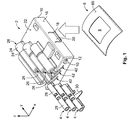
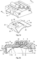
- Figure 1 shows a perspective exploded view of those components which form a receptacle for a free end of a male contact element in form of a PCB.
- Reference numeral 2 denotes a connector housing constituted of a thermoplastic material and made by injection molding. This connector housing 2 receives three contact elements 4 and one spring element 6 being provided with a cut-out section 8.
- the connector housing 2 has an essentially rectangular base surface and a box-like geometry. From lateral side faces 10 upper stops 12 project, which cooperate with a base 14 depicted in Figure 2 . On each lateral side face 10, two upper stops 12 are provided spaced apart in an insertion, or x, direction I. A back surface 16 of the connector housing 2 is provided with a second locking section 18 adapted to project underneath the base 16. This second locking section 18 is provided on a free end of an elastic locking pawl 20 adapted to flex about a swiveling axis which extends in the y direction, i.e. parallel to a plane defined by a top surface 22 of the connector housing 2.
- Respective top surface 22 is projected by convex walls 24 defining three cylindrical receptacles 26 each being provided to receive one of the contact elements 4.
- Each contact element 4 has two opposite longish segments 28 formed by cutting and bending the sheet element depicted in Figure 11 and a contact leg 30 projecting over the longish segments 28 in radial direction.
- the contact element 4 provides securing hooks which are made by bending upward the V-shaped hook sections 32 into the longish segments 28 to at least partially obstruct a cylindrical cable receptacle 34 (cf. Figure 5 or 12 ).
- Respective securing hook is adapted to cooperate with an electrically conductive core of a cable inserted into a cable receptacle 34 to mechanically secure the cable to the contact element 4.
- Both longish segments 28 are designed identical with respect to an axis of symmetry extending through the middle of the contact leg 30.
- Each cable receptacle 34 is provided with a stop made by bending a stop section 36 inwardly into the longish, i.e. cylindrical, segments 28. Respective stop prevents a cable inserted into the cable receptacle 34 from being pushed beyond the assigned cable receptacle 34 of the element 4.
- the bent sheet metal defining the contact element 4 also defines a foot section 38 which is received within a foot receiving slot formed by the connector housing 2 and identified with reference numeral 40 in Figure 5 .
- the contact element inserted into the cylindrical receptacle 26 of the connector housing 2 is arranged within the connector housing 2 in a predetermined radial position. Any bending force generated by the contact leg 30 will not lead to a dislocation of the contact element 4 within the connector housing 2 in radial direction.
- Figures 1 and 5 likewise elucidate a slide-in slot 42 adapted to receive the contact leg 30 when mounting the contact element 4 within the connector housing 2.
- This slide-in slot 42 is open to the lateral side face 10 depicted in Figure 1 for lateral insertion of the contact element 4.
- Respective slide-in slot 42 leads to a contact leg receptacle provided by the connector housing 2 and identified with reference numeral 44 in Figure 5 .
- Respective contact leg receptacle 44 is adapted to receive the contact leg 30 after inserting the contact element 4 into the connector housing 2.
- the contact leg receptacle 44 is provided as a cut-out within the connector housing 2 between two segments of the cylindrical receptacle 26 adapted to receive the longish segments 28 of the contact element 4 in a form-fit manner.
- each contact element 4 is securely received within the connector housing 2 in axial direction.
- the contact element 4 can neither rotate about an axis defined by the cylindrical receptacle 26 nor be pushed out of the cylindrical receptacle 26 nor be dislocated in a radial direction with respect to the cylindrical receptacle 26. Still further, and by cooperation of the foot section 38 and the foot receiving slot 40, the radial position and extension of the contact leg 30 within the connector housing 2 is determined.
- each contact element 4 is spaced apart in the insertion direction I to make contact with a contact surface 46 provided on an upside 48 of a PCB 50. Further, each contact element 4 is spaced apart from the neighboring contact element 4 in the y direction, i.e. perpendicular to the insertion direction I and parallel to a sliding plane, i.e. the x-y plane defined by an upside 52 of the base 14.
- the three contact elements 4 connected to the connector housing 2 are adapted to each abut with their contact leg 30 with the three different contact surfaces 46 provided on the upside 48 of the PCB 50.
- the contact elements 4 are designed identically.
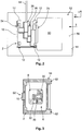
- FIG. 3 shows the base 14 from the underside in a state in which the connector housing 2 is inserted into a receptacle 54 of the base 14 being provided with a central cut-out forming the receptacle 54.
- This receptacle 54 is slightly larger than the circumference of the connector housing 2 to allow a certain degree of movability of the connector housing 2 in the insertion direction I in both the x and the z direction, wherein the x direction corresponds to the insertion direction I, and the y direction is perpendicular to the insertion direction and extends parallel to the upside of the base 14 defining a planar sliding surface 56 for the PCB 50.
- Figure 5 likewise depicts first locking sections 58 which are arranged on the connector housing 2 to project a front surface 60 thereof and project underneath the base 14 for securing the connector housing 2 in a positive manner. For this, the connector housing 2 is first inserted into the receptacle 54 in an inclined orientation to place the first locking section 58 underneath the base 14.
- the connector housing 2 is pivoted in a counter-clockwise direction with respect to the drawing of Figure 5 to slide the second locking section 18 underneath the base 14, thereby pre-tensioning the locking pawl 20 to provide a reliable form fit defining a lower stop 62 preventing the connector housing 2 from being pulled out of the receptacle 54 in the z direction (compare Figure 5 ). After that, the connector housing 2 is allowed to move in the z direction between the lower stops 62 and the upper stops 12.
- stripped wires 64 are inserted into each cable receptacle 34 of each contact element 4 from either one or two sides. The latter being an option for providing multiple PCB interface modules of the present invention in series.
- the stripped cable will inevitably contact the securing hook 32 within the cylindrical receptacle 26 which cuts into the conductive core of the cable 46 and thus secures the cable 46 mechanically to the contact element 4 in an electrically conductive way.
- Figure 5 depicts details of the connection of the spring element 6 within the connector housing 2.
- the connector housing 2 provides opposite supporting surfaces 66, 68 defined by inward steps provided by the connector housing 2 and each defining a support for the spring element 6 which has a curvilinear configuration such that a convex contact surface 69 protrudes towards the contact elements 4.
- the free ends of the contact legs 30 are provided within the cut-out section 8 of the respective spring element 6 in the preassembled state.
- At least one supporting surface 66 is provided as a sliding support for a front abutment surface 70 of the spring element 6 (compare Figure 5 ).
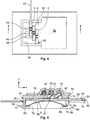
- an insertion opening 74 is recessed in the front surface 60 which is adapted to lead the PCB 50 into the connector housing 2.
- the insertion opening 74 is provided with an upper oblique guiding surface 76 which extends oblique to the sliding surface 56 and guides the PCB 50 towards a planar supporting surface formed by the connector housing 2 and identified with reference numeral 78 in Figures 5 and 6 , respectively.
- the oblique guiding surface 76 leads to the planar supporting surface 78.
- two securing notches 80 are provided at the lateral end sections of the insertion opening 74.
- Those securing notches 80 have a V- shaped configuration projecting as a triangle in cross-sectional direction into the connector housing 2 (compare Figure 6 ). Those securing notches 80 are adapted to cooperate with rectangular form-fit cut-outs 82 provided on the opposite lateral sides of the PCB 50 (compare in particular Figure 7 ). Due to the triangular configuration, the securing notch 80 defines a chamfered guiding surface 84, the function of which will be described hereinafter by referring to Figures 8a to 9 .
- the PCB 50 is arranged on the planar sliding surface 56 provided by the base 14.
- an end face 86 of the PCB 50 comes into contact with the oblique guiding surface 76 thereby pushing the connector housing 2 upward in the z direction (compare Figure 8a, 8b ).
- the upside 48 of the PCB 50 lies against the planar supporting surface 78 provided by the connector housing 2.
- the securing notches 80 are just about to enter into the form-fit cut-outs 82 of the PCB 50. Further advancing the PCB 50 leads to a form-fit connection of the securing notches 80 in the form-fit cut-outs 82.
- This positive locking is secured by the spring force of the spring element 6, which urges the PCB 50 with the planar upside 48 against the planar supporting surface 78 defined by the connector housing 2 (compare Figure 8f ).
- the contact leg 30 is not shown in a deflected state (as is usual in CAD drawings). In fact, the contact leg 30 contacts the upside 52 of the PCB 50, specifically the assigned contact surface 46 of the PCB 50.
- both the PCB 50 and the connector housing 2 may slide in the x direction and/or the z direction without causing any relative movement between the contact surfaces provided between the contact leg 30 and the contact surfaces 46 on the upside 48 of the PCB 50, respectively.
- fretting corrosion is effectively prevented.
- Figures 8a to 9 elucidate vertical floating of the connector housing 2 relative to the base 14 in the course of assembling the PCB 50 within the connector housing 2.
- Figures 10a to 10c elucidate compensation of different PCB thicknesses
- Figure 10a elucidates a preassembled state in which no PCB is received within the connector housing 2
- a rather thin PCB with a thickness of 0.8 mm
- a rather thick PCB with a thickness of 1.8 mm
- Such rather thick PCB 50 leads to a considerable deflection of the spring element 6 in the assembled state.
- the spring element 6 can slide with its abutment surface 70 relative to the supporting surface 66.
- Varying PCB thicknesses lead to differences in the positioning of the connector housing relative to the planar sliding surface 56 provided by the base 14. With a large thickness of the PCB 50, the connector housing 2 is rather lifted ( Figure 10c ), whereas with a thin PCB 50, the connector housing 2 is lowered. The connector housing 2 is moved in the z direction between the upper and lower stops 12, 62.
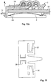
- Figures 14 and 15 elucidate a second embodiment in which the spring element 6 is C-shaped. Sections and functional elements which are identical in the first and the second embodiment are referred to by identical reference numerals.
- the spring element 6 is C-shaped and has a securing end 88 which is adapted to grasp around the rear end of the connector housing 2 and provided with a holding cut-out 90 recessed in the planar securing end 88 and adapted to cooperate with the holding projection 92 unitarily formed by the connector housing 2.
- the securing end 88 and an intermediate section 94 of the spring element 6 are bent to include an angle smaller than 90°. After clamping the C-shaped configuration of the spring element 6 against the connector housing 2, the securing end 88 and the intermediate section 94 of the spring element 6 lie against perpendicular outer surfaces of the connector housing under pre-tension, while the holding projection 92 extends through the holding cut-out 90. Thus, the spring element 6 is securely attached to the connector housing 2.
- the spring element 6 is provided with a cut-out section 8.
- a further cut-out 96 is provided in the transition between the intermediate section 94 and the curvilinear contact surface 69 to expose the locking pawl 20 and the second locking section 18 to allow a swiveling movement of the locking pawl 20.
- the cut-out section 8 receives the front ends of the contact legs 30 projecting below the planar supporting surface 78 for the PCB 50.
- the other end of the spring element 6 is freely suspended within the insertion opening 74.
- the spring element 6 provides a planar spring sliding surface 98 which extends essentially parallel to the planar supporting surface 78.
- the free end of the spring element 6 has been projected underneath the base 14.
- a PCB sliding over the planar sliding surface 56 is eventually pushed on the upside of the spring sliding surface 98 to advance into the connector housing 2.
- the chamfered guiding surface 84 continues with the inclination and direction of the oblique guiding surface 78.
- a continuous guiding for an end face 86 of the PCB 50 is provided.
- the C-shaped spring element 6 can be connected to the connector housing 2 at a rather solid rear end thereof.
- the connection is more durable and can sustain stronger bending such as e.g. spring forces acting against the PCB 50 to hold the same against the planar supporting surface 78 provided by the connector housing 2.
Landscapes
- Connector Housings Or Holding Contact Members (AREA)
- Details Of Connecting Devices For Male And Female Coupling (AREA)
Claims (14)
- Schnittstellen-Modul, das umfasst:ein Verbinder-Gehäuse (2), das aus einem elektrisch isolierenden Material besteht, wobei das Verbinder-Gehäuse (2) wenigstens ein Kontaktelement (4) aufnimmt, das Kontaktelement (4) mit einem Kontakt-Schenkel (30) versehen ist, der unterhalb einer ebenen Trage-Fläche (78) vorsteht und mit einer Kontakt-Fläche (46) an der Oberfläche eines Einführ-Kontaktelementes in einem vormontierten Zustand in Kontakt ist, wobei die ebene Trage-Fläche (78) durch das Verbinder-Gehäuse (2) gebildet wird,dadurch gekennzeichnet, dassdas Schnittstellen-Modul des Weiteren umfasst:ein Federelement (6), das so eingerichtet ist, dass es in einem montierten Zustand des Einführ-Kontaktelementes (50) elastisch an einer Unterseite des Einführ-Kontakt-elementes (50) anliegt, wobei in dem montierten Zustand der Kontakt-Schenkel (30) des wenigstens einen Kontaktelementes (4) an der Kontaktfläche (46) an einer Oberseite (48) des Einführ-Kontaktelementes (50) anliegt und die Oberseite (48) des Einführ-Kontaktelementes (50) aufgrund des Federelementes (6) an der ebenen Trage-Fläche (78) anliegt, undeine Auflage (14), die eine ebene Gleitfläche (56) für das Einführ- Kontaktelement (50) bildet,dadurch, dass das Verbinder-Gehäuse (2) beweglich in einer Aufnahme (54) der Auflage (14) aufgenommen ist,dass das Kontaktelement (4) oberhalb der Gleitfläche (56) angeordnet ist,dass das Verbinder-Gehäuse (2) eine Einführöffnung (74) aufweist, die zum Aufnehmen des Einführ-Kontaktelementes (50) eingerichtet ist,dass das Federelement (6) dem wenigstens einen Kontaktelement (4) in einer Richtung senkrecht zu der Gleitfläche (56) gegenüberliegend angeordnet ist, unddass das Einführ-Kontaktelement (50) in dem montierten Zustand im Inneren der Einführöffnung (74) des Verbinder-Gehäuses (2) aufgenommen ist.
- Schnittstellen-Modul nach Anspruch 1, dadurch gekennzeichnet, dass das Verbinder-Gehäuse (2) in einer Richtung (Z) senkrecht zu der Gleitfläche (56) zwischen einem oberen und einem unteren Anschlag (12; 62) bewegt werden kann.
- Schnittstellen-Modul nach Anspruch 1 oder 2, dadurch gekennzeichnet, dassdas Kontaktelement (4) wenigstens ein längliches Segment (28) aufweist, das so eingerichtet ist, dass es ein Kabel (64) aufnimmt und elektrisch mit ihm verbunden ist, und dass das Verbinder-Gehäuse (2) eine zylindrische Aufnahme (26) bildet, die so eingerichtet ist, dass sie das Kontaktelement (4) in einer vorgegebenen radialen Position aufnimmt, in der der Kontakt-Schenkel (30) unterhalb der ebenen Trage-Fläche (78) für das Einführ-Kontaktelement (50) in dem vormontierten Zustand vorsteht.
- Schnittstellen-Modul nach Anspruch 3, dadurch gekennzeichnet, dass das Kontaktelement (4) gegenüberliegende längliche Segmente (28) aufweist, die jeweils so eingerichtet sind, dass sie das Kabel (64) von einander gegenüberliegenden Seiten aufnehmen und elektrisch mit ihm verbunden sind, und der Kontakt-Schenkel (30) zwischen ihnen angeordnet ist.
- Schnittstellen-Modul nach Anspruch 3 oder 4, dadurch gekennzeichnet, dassdas Kontaktelement (4) an dem Verbinder-Gehäuse (2) so befestigt ist, dass es eine vorgegebene Position in einer axialen Richtung der zylindrischen Aufnahme (26) einnimmt.
- Schnittstellen-Modul nach einem der vorangehenden Ansprüche, dadurch gekennzeichnet, dass das Verbinder-Gehäuse (2) eine von der ebenen Trage-Fläche (78) vorstehende Sicherungs-Nase (80) aufweist, das Einführ-Kontaktelement (50) einen formschlüssigen Ausschnitt (82) aufweist, in dem die Sicherungs-Nase (80) in dem montierten Zustand aufgenommen ist, und dass das Verbinder-Gehäuse (2) in einer Einführ-Richtung (I) des Einführ-Kontaktelementes (50) in das Verbinder-Gehäuse (2) hinein gleitend in der Aufnahme aufgenommen wird.
- Schnittstellen-Modul nach Anspruch 6, dadurch gekennzeichnet, dass sich die Sicherungs-Nase (80) an der Einführöffnung (74) befindet und eine abgeschrägte Führungsfläche (84) aufweist, die so eingerichtet ist, dass sie mit dem Einführ-Kontaktelement (50) zusammenwirkt, um das Einführ-Kontaktelement (50) unter die durch das Verbinder-Gehäuse (2) gebildete ebene Trage-Fläche (78) für das Einführ-Kontaktelement (50) zu drücken.
- Schnittstellen-Modul nach einem der vorangehenden Ansprüche, dadurch gekennzeichnet, dass das Federelement (6) an dem Verbinder-Gehäuse (2) befestigt ist.
- Schnittstellen-Modul nach Anspruch 8, dadurch gekennzeichnet, dass das Federelement (6) in Bezug auf die Einführ-Richtung (I) einander gegenüberliegende Anliegeflächen (70; 72) aufweist, die mit einander gegenüberliegenden Auflageflächen (66; 68) des Verbinder-Gehäuses (2) zusammenwirken, und dass wenigstens eine der einander gegenüberliegenden Anliegeflächen (70; 72) gleitend an den zugehörigen Auflageflächen (66; 68) des Verbinder-Gehäuses gleitend aufliegt.
- Schnittstellen-Modul nach Anspruch 8, dadurch gekennzeichnet, dass das Federelement (6) einen C-förmigen Aufbau hat und mit einem Sicherungs-Ende (88) an dem Verbinder-Gehäuse (2) befestigt ist und dass das andere Ende des Federelementes (6) in der Nähe der Einführöffnung (74) frei schwebt.
- Schnittstellen-Modul nach Anspruch 10, dadurch gekennzeichnet, dass das andere Ende des Federelementes (6) eine ebene Feder-Gleitfläche (98) aufweist, die sich im Wesentlichen parallel zu der ebenen Gleitfläche (56) erstreckt, die durch die Auflage (14) gebildet wird.
- Schnittstellen-Modul nach einem der vorangehenden Ansprüche, dadurch gekennzeichnet, dass das Federelement (6) durch ein aus einem Stück bestehendes Blech gebildet wird, das mit einem ausgeschnittenen Teil (8) versehen ist, in dem der wenigstens eine Kontakt-Schenkel (30) in dem vormontierten Zustand angeordnet ist, und dass das Federelement (6) eine gekrümmte, zu dem Kontaktelement (4) hin vorstehende Kontaktfläche (69) aufweist.
- Schnittstellen-Modul nach einem der vorangehenden Ansprüche, gekennzeichnet durch wenigstens zwei Kontaktelemente (4), wobei die Kontakt-Schenkel (30) der Kontaktelemente (4) senkrecht zu einer Einführ-Richtung (I) des Einführ-Kontaktelementes (50) in das Verbinder-Gehäuse (2) hinein beabstandet sind, und die Kontaktelemente (4) in der Einführ-Richtung (I) des Einführ-Kontaktelementes (50) in das Verbindergehäuse (2) hinein beabstandet sind.
- Schnittstellen-Modul nach einem der vorangehenden Ansprüche, dadurch gekennzeichnet, dass das Verbinder-Gehäuse (2) einen ersten Arretierabschnitt (58) und einen zweiten Arretierabschnitt (18) aufweist, die sich jeweils an entgegengesetzten Enden des Verbindergehäuses (2) befinden und jeweils so eingerichtet sind, dass sie unterhalb der Auflage (14) vorstehen, wobei sich der zweite Arretierabschnitt (18) an einem freien Ende einer elastischen Arretierklinke (20) befindet, und der erste sowie der zweite Arretierabschnitt (58; 18) untere Anschläge (62) aufweisen, die eine Beweglichkeit des Verbinder-Gehäuses (2) in einer Richtung senkrecht zu der Gleitfläche (56) begrenzen.
Priority Applications (2)
| Application Number | Priority Date | Filing Date | Title |
|---|---|---|---|
| EP17189976.8A EP3454425B1 (de) | 2017-09-07 | 2017-09-07 | Schnittstellenmodul |
| US16/124,538 US10404003B2 (en) | 2017-09-07 | 2018-09-07 | Interface module |
Applications Claiming Priority (1)
| Application Number | Priority Date | Filing Date | Title |
|---|---|---|---|
| EP17189976.8A EP3454425B1 (de) | 2017-09-07 | 2017-09-07 | Schnittstellenmodul |
Publications (2)
| Publication Number | Publication Date |
|---|---|
| EP3454425A1 EP3454425A1 (de) | 2019-03-13 |
| EP3454425B1 true EP3454425B1 (de) | 2020-04-08 |
Family
ID=59811252
Family Applications (1)
| Application Number | Title | Priority Date | Filing Date |
|---|---|---|---|
| EP17189976.8A Active EP3454425B1 (de) | 2017-09-07 | 2017-09-07 | Schnittstellenmodul |
Country Status (2)
| Country | Link |
|---|---|
| US (1) | US10404003B2 (de) |
| EP (1) | EP3454425B1 (de) |
Families Citing this family (2)
| Publication number | Priority date | Publication date | Assignee | Title |
|---|---|---|---|---|
| US11063345B2 (en) * | 2018-07-17 | 2021-07-13 | Mastodon Design Llc | Systems and methods for providing a wearable antenna |
| US11171438B2 (en) * | 2020-04-09 | 2021-11-09 | Energy Services LLC | Unitized cable plug array for mobile power generation equipment |
Family Cites Families (6)
| Publication number | Priority date | Publication date | Assignee | Title |
|---|---|---|---|---|
| ZA712691B (en) | 1970-05-22 | 1972-01-26 | Amp Inc | Contact element for a printed circuit edge connector |
| KR100650863B1 (ko) | 2005-10-24 | 2006-11-27 | 주식회사 팬택앤큐리텔 | 사용자 인증 카드 소켓 겸용 내장형 안테나 캐리어를구비하는 휴대용 단말기 |
| DE102012012087B4 (de) * | 2012-06-14 | 2019-01-17 | H & B Electronic Gmbh & Co. Kg | Elektrischer Steckverbinder |
| KR102095013B1 (ko) * | 2013-04-11 | 2020-03-31 | 삼성디스플레이 주식회사 | 플렉서블 장치 |
| US9166319B2 (en) * | 2013-10-17 | 2015-10-20 | Tyco Electronics Corporation | Flexible circuit board connector |
| KR102384576B1 (ko) * | 2015-06-15 | 2022-04-08 | 엘지디스플레이 주식회사 | 플렉서블 표시 장치 |
-
2017
- 2017-09-07 EP EP17189976.8A patent/EP3454425B1/de active Active
-
2018
- 2018-09-07 US US16/124,538 patent/US10404003B2/en active Active
Non-Patent Citations (1)
| Title |
|---|
| None * |
Also Published As
| Publication number | Publication date |
|---|---|
| EP3454425A1 (de) | 2019-03-13 |
| US20190074624A1 (en) | 2019-03-07 |
| US10404003B2 (en) | 2019-09-03 |
Similar Documents
| Publication | Publication Date | Title |
|---|---|---|
| EP2863482B1 (de) | Flexibler Leiterplattenverbinder | |
| EP3095160B1 (de) | Elektrischer verbinder mit anschlusspositionsbestätigung | |
| US7887350B2 (en) | Floating connector with a fixture to limit vertical movement of the connector | |
| US6178106B1 (en) | Power distribution center with improved power supply connection | |
| EP3198682B1 (de) | Elektrischer verbinder mit schwenkblock zum anschliessen eines elektrodraht | |
| US5413497A (en) | Electrical connector | |
| EP2642606B1 (de) | Verbindereinheit | |
| US9450319B2 (en) | Cable connector and connector device having the same | |
| EP3149809B1 (de) | Elektrischer verbinder zur verwendung mit bestückten leiterplatten | |
| US11374358B2 (en) | Wire to board connector with low height | |
| HK1000396B (en) | Electrical connector | |
| US20130034984A1 (en) | Latch for a card edge connector system | |
| US9673542B1 (en) | Poke-in electrical connector having a contact with a base extending through an opening in a bottom of a housing | |
| EP3454425B1 (de) | Schnittstellenmodul | |
| US4508410A (en) | Electrical termination system and connector member | |
| EP3181987A1 (de) | Led-fassung zur aufnahme einer cob-led und basis für eine solche led-fassung | |
| EP0390449B1 (de) | Elektrischer Verbinder | |
| US20020127904A1 (en) | Relay connector | |
| US5860825A (en) | Socket for printed circuit board | |
| EP3703195B1 (de) | Anschlussklemme für verbinder und verbinder damit | |
| US20180226732A1 (en) | Connection housing with a connection device for conductors | |
| US20260011934A1 (en) | Wire Clamping Assembly and Connector Arrangement | |
| JP7811361B2 (ja) | コネクタ | |
| JP4911712B2 (ja) | 電気コネクタ組立体 | |
| EP1006616B1 (de) | Elektrischer Verbinder |
Legal Events
| Date | Code | Title | Description |
|---|---|---|---|
| PUAI | Public reference made under article 153(3) epc to a published international application that has entered the european phase |
Free format text: ORIGINAL CODE: 0009012 |
|
| STAA | Information on the status of an ep patent application or granted ep patent |
Free format text: STATUS: THE APPLICATION HAS BEEN PUBLISHED |
|
| AK | Designated contracting states |
Kind code of ref document: A1 Designated state(s): AL AT BE BG CH CY CZ DE DK EE ES FI FR GB GR HR HU IE IS IT LI LT LU LV MC MK MT NL NO PL PT RO RS SE SI SK SM TR |
|
| AX | Request for extension of the european patent |
Extension state: BA ME |
|
| STAA | Information on the status of an ep patent application or granted ep patent |
Free format text: STATUS: REQUEST FOR EXAMINATION WAS MADE |
|
| 17P | Request for examination filed |
Effective date: 20190829 |
|
| RBV | Designated contracting states (corrected) |
Designated state(s): AL AT BE BG CH CY CZ DE DK EE ES FI FR GB GR HR HU IE IS IT LI LT LU LV MC MK MT NL NO PL PT RO RS SE SI SK SM TR |
|
| GRAP | Despatch of communication of intention to grant a patent |
Free format text: ORIGINAL CODE: EPIDOSNIGR1 |
|
| STAA | Information on the status of an ep patent application or granted ep patent |
Free format text: STATUS: GRANT OF PATENT IS INTENDED |
|
| RIC1 | Information provided on ipc code assigned before grant |
Ipc: H01R 12/71 20110101AFI20191031BHEP Ipc: H01R 12/85 20110101ALI20191031BHEP |
|
| INTG | Intention to grant announced |
Effective date: 20191119 |
|
| GRAS | Grant fee paid |
Free format text: ORIGINAL CODE: EPIDOSNIGR3 |
|
| GRAA | (expected) grant |
Free format text: ORIGINAL CODE: 0009210 |
|
| STAA | Information on the status of an ep patent application or granted ep patent |
Free format text: STATUS: THE PATENT HAS BEEN GRANTED |
|
| AK | Designated contracting states |
Kind code of ref document: B1 Designated state(s): AL AT BE BG CH CY CZ DE DK EE ES FI FR GB GR HR HU IE IS IT LI LT LU LV MC MK MT NL NO PL PT RO RS SE SI SK SM TR |
|
| REG | Reference to a national code |
Ref country code: CH Ref legal event code: EP Ref country code: AT Ref legal event code: REF Ref document number: 1255610 Country of ref document: AT Kind code of ref document: T Effective date: 20200415 |
|
| REG | Reference to a national code |
Ref country code: DE Ref legal event code: R096 Ref document number: 602017014271 Country of ref document: DE |
|
| REG | Reference to a national code |
Ref country code: IE Ref legal event code: FG4D |
|
| REG | Reference to a national code |
Ref country code: NL Ref legal event code: MP Effective date: 20200408 |
|
| REG | Reference to a national code |
Ref country code: LT Ref legal event code: MG4D |
|
| PG25 | Lapsed in a contracting state [announced via postgrant information from national office to epo] |
Ref country code: FI Free format text: LAPSE BECAUSE OF FAILURE TO SUBMIT A TRANSLATION OF THE DESCRIPTION OR TO PAY THE FEE WITHIN THE PRESCRIBED TIME-LIMIT Effective date: 20200408 Ref country code: NO Free format text: LAPSE BECAUSE OF FAILURE TO SUBMIT A TRANSLATION OF THE DESCRIPTION OR TO PAY THE FEE WITHIN THE PRESCRIBED TIME-LIMIT Effective date: 20200708 Ref country code: PT Free format text: LAPSE BECAUSE OF FAILURE TO SUBMIT A TRANSLATION OF THE DESCRIPTION OR TO PAY THE FEE WITHIN THE PRESCRIBED TIME-LIMIT Effective date: 20200817 Ref country code: LT Free format text: LAPSE BECAUSE OF FAILURE TO SUBMIT A TRANSLATION OF THE DESCRIPTION OR TO PAY THE FEE WITHIN THE PRESCRIBED TIME-LIMIT Effective date: 20200408 Ref country code: IS Free format text: LAPSE BECAUSE OF FAILURE TO SUBMIT A TRANSLATION OF THE DESCRIPTION OR TO PAY THE FEE WITHIN THE PRESCRIBED TIME-LIMIT Effective date: 20200808 Ref country code: SE Free format text: LAPSE BECAUSE OF FAILURE TO SUBMIT A TRANSLATION OF THE DESCRIPTION OR TO PAY THE FEE WITHIN THE PRESCRIBED TIME-LIMIT Effective date: 20200408 Ref country code: GR Free format text: LAPSE BECAUSE OF FAILURE TO SUBMIT A TRANSLATION OF THE DESCRIPTION OR TO PAY THE FEE WITHIN THE PRESCRIBED TIME-LIMIT Effective date: 20200709 Ref country code: NL Free format text: LAPSE BECAUSE OF FAILURE TO SUBMIT A TRANSLATION OF THE DESCRIPTION OR TO PAY THE FEE WITHIN THE PRESCRIBED TIME-LIMIT Effective date: 20200408 |
|
| REG | Reference to a national code |
Ref country code: AT Ref legal event code: MK05 Ref document number: 1255610 Country of ref document: AT Kind code of ref document: T Effective date: 20200408 |
|
| PG25 | Lapsed in a contracting state [announced via postgrant information from national office to epo] |
Ref country code: RS Free format text: LAPSE BECAUSE OF FAILURE TO SUBMIT A TRANSLATION OF THE DESCRIPTION OR TO PAY THE FEE WITHIN THE PRESCRIBED TIME-LIMIT Effective date: 20200408 Ref country code: BG Free format text: LAPSE BECAUSE OF FAILURE TO SUBMIT A TRANSLATION OF THE DESCRIPTION OR TO PAY THE FEE WITHIN THE PRESCRIBED TIME-LIMIT Effective date: 20200708 Ref country code: LV Free format text: LAPSE BECAUSE OF FAILURE TO SUBMIT A TRANSLATION OF THE DESCRIPTION OR TO PAY THE FEE WITHIN THE PRESCRIBED TIME-LIMIT Effective date: 20200408 Ref country code: HR Free format text: LAPSE BECAUSE OF FAILURE TO SUBMIT A TRANSLATION OF THE DESCRIPTION OR TO PAY THE FEE WITHIN THE PRESCRIBED TIME-LIMIT Effective date: 20200408 |
|
| PG25 | Lapsed in a contracting state [announced via postgrant information from national office to epo] |
Ref country code: AL Free format text: LAPSE BECAUSE OF FAILURE TO SUBMIT A TRANSLATION OF THE DESCRIPTION OR TO PAY THE FEE WITHIN THE PRESCRIBED TIME-LIMIT Effective date: 20200408 |
|
| REG | Reference to a national code |
Ref country code: DE Ref legal event code: R097 Ref document number: 602017014271 Country of ref document: DE |
|
| PG25 | Lapsed in a contracting state [announced via postgrant information from national office to epo] |
Ref country code: ES Free format text: LAPSE BECAUSE OF FAILURE TO SUBMIT A TRANSLATION OF THE DESCRIPTION OR TO PAY THE FEE WITHIN THE PRESCRIBED TIME-LIMIT Effective date: 20200408 Ref country code: DK Free format text: LAPSE BECAUSE OF FAILURE TO SUBMIT A TRANSLATION OF THE DESCRIPTION OR TO PAY THE FEE WITHIN THE PRESCRIBED TIME-LIMIT Effective date: 20200408 Ref country code: SM Free format text: LAPSE BECAUSE OF FAILURE TO SUBMIT A TRANSLATION OF THE DESCRIPTION OR TO PAY THE FEE WITHIN THE PRESCRIBED TIME-LIMIT Effective date: 20200408 Ref country code: IT Free format text: LAPSE BECAUSE OF FAILURE TO SUBMIT A TRANSLATION OF THE DESCRIPTION OR TO PAY THE FEE WITHIN THE PRESCRIBED TIME-LIMIT Effective date: 20200408 Ref country code: CZ Free format text: LAPSE BECAUSE OF FAILURE TO SUBMIT A TRANSLATION OF THE DESCRIPTION OR TO PAY THE FEE WITHIN THE PRESCRIBED TIME-LIMIT Effective date: 20200408 Ref country code: EE Free format text: LAPSE BECAUSE OF FAILURE TO SUBMIT A TRANSLATION OF THE DESCRIPTION OR TO PAY THE FEE WITHIN THE PRESCRIBED TIME-LIMIT Effective date: 20200408 Ref country code: AT Free format text: LAPSE BECAUSE OF FAILURE TO SUBMIT A TRANSLATION OF THE DESCRIPTION OR TO PAY THE FEE WITHIN THE PRESCRIBED TIME-LIMIT Effective date: 20200408 Ref country code: RO Free format text: LAPSE BECAUSE OF FAILURE TO SUBMIT A TRANSLATION OF THE DESCRIPTION OR TO PAY THE FEE WITHIN THE PRESCRIBED TIME-LIMIT Effective date: 20200408 |
|
| PLBE | No opposition filed within time limit |
Free format text: ORIGINAL CODE: 0009261 |
|
| STAA | Information on the status of an ep patent application or granted ep patent |
Free format text: STATUS: NO OPPOSITION FILED WITHIN TIME LIMIT |
|
| PG25 | Lapsed in a contracting state [announced via postgrant information from national office to epo] |
Ref country code: PL Free format text: LAPSE BECAUSE OF FAILURE TO SUBMIT A TRANSLATION OF THE DESCRIPTION OR TO PAY THE FEE WITHIN THE PRESCRIBED TIME-LIMIT Effective date: 20200408 Ref country code: SK Free format text: LAPSE BECAUSE OF FAILURE TO SUBMIT A TRANSLATION OF THE DESCRIPTION OR TO PAY THE FEE WITHIN THE PRESCRIBED TIME-LIMIT Effective date: 20200408 |
|
| 26N | No opposition filed |
Effective date: 20210112 |
|
| REG | Reference to a national code |
Ref country code: CH Ref legal event code: PL |
|
| PG25 | Lapsed in a contracting state [announced via postgrant information from national office to epo] |
Ref country code: SI Free format text: LAPSE BECAUSE OF FAILURE TO SUBMIT A TRANSLATION OF THE DESCRIPTION OR TO PAY THE FEE WITHIN THE PRESCRIBED TIME-LIMIT Effective date: 20200408 |
|
| REG | Reference to a national code |
Ref country code: BE Ref legal event code: MM Effective date: 20200930 |
|
| PG25 | Lapsed in a contracting state [announced via postgrant information from national office to epo] |
Ref country code: LU Free format text: LAPSE BECAUSE OF NON-PAYMENT OF DUE FEES Effective date: 20200907 |
|
| PG25 | Lapsed in a contracting state [announced via postgrant information from national office to epo] |
Ref country code: LI Free format text: LAPSE BECAUSE OF NON-PAYMENT OF DUE FEES Effective date: 20200930 Ref country code: IE Free format text: LAPSE BECAUSE OF NON-PAYMENT OF DUE FEES Effective date: 20200907 Ref country code: CH Free format text: LAPSE BECAUSE OF NON-PAYMENT OF DUE FEES Effective date: 20200930 Ref country code: BE Free format text: LAPSE BECAUSE OF NON-PAYMENT OF DUE FEES Effective date: 20200930 |
|
| PG25 | Lapsed in a contracting state [announced via postgrant information from national office to epo] |
Ref country code: TR Free format text: LAPSE BECAUSE OF FAILURE TO SUBMIT A TRANSLATION OF THE DESCRIPTION OR TO PAY THE FEE WITHIN THE PRESCRIBED TIME-LIMIT Effective date: 20200408 Ref country code: MT Free format text: LAPSE BECAUSE OF FAILURE TO SUBMIT A TRANSLATION OF THE DESCRIPTION OR TO PAY THE FEE WITHIN THE PRESCRIBED TIME-LIMIT Effective date: 20200408 Ref country code: CY Free format text: LAPSE BECAUSE OF FAILURE TO SUBMIT A TRANSLATION OF THE DESCRIPTION OR TO PAY THE FEE WITHIN THE PRESCRIBED TIME-LIMIT Effective date: 20200408 |
|
| PG25 | Lapsed in a contracting state [announced via postgrant information from national office to epo] |
Ref country code: MK Free format text: LAPSE BECAUSE OF FAILURE TO SUBMIT A TRANSLATION OF THE DESCRIPTION OR TO PAY THE FEE WITHIN THE PRESCRIBED TIME-LIMIT Effective date: 20200408 Ref country code: MC Free format text: LAPSE BECAUSE OF FAILURE TO SUBMIT A TRANSLATION OF THE DESCRIPTION OR TO PAY THE FEE WITHIN THE PRESCRIBED TIME-LIMIT Effective date: 20200408 |
|
| PGFP | Annual fee paid to national office [announced via postgrant information from national office to epo] |
Ref country code: GB Payment date: 20240701 Year of fee payment: 8 |
|
| PGFP | Annual fee paid to national office [announced via postgrant information from national office to epo] |
Ref country code: FR Payment date: 20240702 Year of fee payment: 8 |
|
| PGFP | Annual fee paid to national office [announced via postgrant information from national office to epo] |
Ref country code: DE Payment date: 20250702 Year of fee payment: 9 |