EP3454350A2 - Power semiconductor systems having inductor modules, and methods of manufacturing inductor modules and power semiconductor systems having inductor modules - Google Patents
Power semiconductor systems having inductor modules, and methods of manufacturing inductor modules and power semiconductor systems having inductor modules Download PDFInfo
- Publication number
- EP3454350A2 EP3454350A2 EP18192632.0A EP18192632A EP3454350A2 EP 3454350 A2 EP3454350 A2 EP 3454350A2 EP 18192632 A EP18192632 A EP 18192632A EP 3454350 A2 EP3454350 A2 EP 3454350A2
- Authority
- EP
- European Patent Office
- Prior art keywords
- inductor
- ferrite sheet
- insulating material
- module
- power stage
- Prior art date
- Legal status (The legal status is an assumption and is not a legal conclusion. Google has not performed a legal analysis and makes no representation as to the accuracy of the status listed.)
- Granted
Links
Images













Classifications
-
- H—ELECTRICITY
- H02—GENERATION; CONVERSION OR DISTRIBUTION OF ELECTRIC POWER
- H02M—APPARATUS FOR CONVERSION BETWEEN AC AND AC, BETWEEN AC AND DC, OR BETWEEN DC AND DC, AND FOR USE WITH MAINS OR SIMILAR POWER SUPPLY SYSTEMS; CONVERSION OF DC OR AC INPUT POWER INTO SURGE OUTPUT POWER; CONTROL OR REGULATION THEREOF
- H02M3/00—Conversion of DC power input into DC power output
- H02M3/02—Conversion of DC power input into DC power output without intermediate conversion into AC
- H02M3/04—Conversion of DC power input into DC power output without intermediate conversion into AC by static converters
- H02M3/10—Conversion of DC power input into DC power output without intermediate conversion into AC by static converters using discharge tubes with control electrode or semiconductor devices with control electrode
- H02M3/145—Conversion of DC power input into DC power output without intermediate conversion into AC by static converters using discharge tubes with control electrode or semiconductor devices with control electrode using devices of a triode or transistor type requiring continuous application of a control signal
- H02M3/155—Conversion of DC power input into DC power output without intermediate conversion into AC by static converters using discharge tubes with control electrode or semiconductor devices with control electrode using devices of a triode or transistor type requiring continuous application of a control signal using semiconductor devices only
-
- H—ELECTRICITY
- H01—ELECTRIC ELEMENTS
- H01F—MAGNETS; INDUCTANCES; TRANSFORMERS; SELECTION OF MATERIALS FOR THEIR MAGNETIC PROPERTIES
- H01F17/00—Fixed inductances of the signal type
- H01F17/0006—Printed inductances
- H01F17/0033—Printed inductances with the coil helically wound around a magnetic core
-
- H—ELECTRICITY
- H01—ELECTRIC ELEMENTS
- H01F—MAGNETS; INDUCTANCES; TRANSFORMERS; SELECTION OF MATERIALS FOR THEIR MAGNETIC PROPERTIES
- H01F17/00—Fixed inductances of the signal type
- H01F17/04—Fixed inductances of the signal type with magnetic core
- H01F17/06—Fixed inductances of the signal type with magnetic core with core substantially closed in itself, e.g. toroid
- H01F17/062—Toroidal core with turns of coil around it
-
- H—ELECTRICITY
- H01—ELECTRIC ELEMENTS
- H01F—MAGNETS; INDUCTANCES; TRANSFORMERS; SELECTION OF MATERIALS FOR THEIR MAGNETIC PROPERTIES
- H01F27/00—Details of transformers or inductances, in general
- H01F27/06—Mounting, supporting, or suspending transformers, reactors, or choke coils not being of the signal type
- H01F27/065—Mounting on printed circuit boards
-
- H—ELECTRICITY
- H01—ELECTRIC ELEMENTS
- H01F—MAGNETS; INDUCTANCES; TRANSFORMERS; SELECTION OF MATERIALS FOR THEIR MAGNETIC PROPERTIES
- H01F27/00—Details of transformers or inductances, in general
- H01F27/24—Magnetic cores
-
- H—ELECTRICITY
- H01—ELECTRIC ELEMENTS
- H01F—MAGNETS; INDUCTANCES; TRANSFORMERS; SELECTION OF MATERIALS FOR THEIR MAGNETIC PROPERTIES
- H01F27/00—Details of transformers or inductances, in general
- H01F27/24—Magnetic cores
- H01F27/245—Magnetic cores made from sheets, e.g. grain-oriented
-
- H—ELECTRICITY
- H01—ELECTRIC ELEMENTS
- H01F—MAGNETS; INDUCTANCES; TRANSFORMERS; SELECTION OF MATERIALS FOR THEIR MAGNETIC PROPERTIES
- H01F27/00—Details of transformers or inductances, in general
- H01F27/24—Magnetic cores
- H01F27/255—Magnetic cores made from particles
-
- H—ELECTRICITY
- H01—ELECTRIC ELEMENTS
- H01F—MAGNETS; INDUCTANCES; TRANSFORMERS; SELECTION OF MATERIALS FOR THEIR MAGNETIC PROPERTIES
- H01F27/00—Details of transformers or inductances, in general
- H01F27/28—Coils; Windings; Conductive connections
- H01F27/2804—Printed windings
-
- H—ELECTRICITY
- H01—ELECTRIC ELEMENTS
- H01F—MAGNETS; INDUCTANCES; TRANSFORMERS; SELECTION OF MATERIALS FOR THEIR MAGNETIC PROPERTIES
- H01F37/00—Fixed inductances not covered by group H01F17/00
-
- H—ELECTRICITY
- H01—ELECTRIC ELEMENTS
- H01F—MAGNETS; INDUCTANCES; TRANSFORMERS; SELECTION OF MATERIALS FOR THEIR MAGNETIC PROPERTIES
- H01F41/00—Apparatus or processes specially adapted for manufacturing or assembling magnets, inductances or transformers; Apparatus or processes specially adapted for manufacturing materials characterised by their magnetic properties
-
- H—ELECTRICITY
- H01—ELECTRIC ELEMENTS
- H01F—MAGNETS; INDUCTANCES; TRANSFORMERS; SELECTION OF MATERIALS FOR THEIR MAGNETIC PROPERTIES
- H01F41/00—Apparatus or processes specially adapted for manufacturing or assembling magnets, inductances or transformers; Apparatus or processes specially adapted for manufacturing materials characterised by their magnetic properties
- H01F41/02—Apparatus or processes specially adapted for manufacturing or assembling magnets, inductances or transformers; Apparatus or processes specially adapted for manufacturing materials characterised by their magnetic properties for manufacturing cores, coils, or magnets
-
- H—ELECTRICITY
- H01—ELECTRIC ELEMENTS
- H01F—MAGNETS; INDUCTANCES; TRANSFORMERS; SELECTION OF MATERIALS FOR THEIR MAGNETIC PROPERTIES
- H01F41/00—Apparatus or processes specially adapted for manufacturing or assembling magnets, inductances or transformers; Apparatus or processes specially adapted for manufacturing materials characterised by their magnetic properties
- H01F41/02—Apparatus or processes specially adapted for manufacturing or assembling magnets, inductances or transformers; Apparatus or processes specially adapted for manufacturing materials characterised by their magnetic properties for manufacturing cores, coils, or magnets
- H01F41/04—Apparatus or processes specially adapted for manufacturing or assembling magnets, inductances or transformers; Apparatus or processes specially adapted for manufacturing materials characterised by their magnetic properties for manufacturing cores, coils, or magnets for manufacturing coils
- H01F41/041—Printed circuit coils
-
- H—ELECTRICITY
- H01—ELECTRIC ELEMENTS
- H01F—MAGNETS; INDUCTANCES; TRANSFORMERS; SELECTION OF MATERIALS FOR THEIR MAGNETIC PROPERTIES
- H01F41/00—Apparatus or processes specially adapted for manufacturing or assembling magnets, inductances or transformers; Apparatus or processes specially adapted for manufacturing materials characterised by their magnetic properties
- H01F41/02—Apparatus or processes specially adapted for manufacturing or assembling magnets, inductances or transformers; Apparatus or processes specially adapted for manufacturing materials characterised by their magnetic properties for manufacturing cores, coils, or magnets
- H01F41/04—Apparatus or processes specially adapted for manufacturing or assembling magnets, inductances or transformers; Apparatus or processes specially adapted for manufacturing materials characterised by their magnetic properties for manufacturing cores, coils, or magnets for manufacturing coils
- H01F41/041—Printed circuit coils
- H01F41/046—Printed circuit coils structurally combined with ferromagnetic material
-
- H—ELECTRICITY
- H02—GENERATION; CONVERSION OR DISTRIBUTION OF ELECTRIC POWER
- H02M—APPARATUS FOR CONVERSION BETWEEN AC AND AC, BETWEEN AC AND DC, OR BETWEEN DC AND DC, AND FOR USE WITH MAINS OR SIMILAR POWER SUPPLY SYSTEMS; CONVERSION OF DC OR AC INPUT POWER INTO SURGE OUTPUT POWER; CONTROL OR REGULATION THEREOF
- H02M1/00—Details of apparatus for conversion
- H02M1/0048—Circuits or arrangements for reducing losses
-
- H—ELECTRICITY
- H02—GENERATION; CONVERSION OR DISTRIBUTION OF ELECTRIC POWER
- H02M—APPARATUS FOR CONVERSION BETWEEN AC AND AC, BETWEEN AC AND DC, OR BETWEEN DC AND DC, AND FOR USE WITH MAINS OR SIMILAR POWER SUPPLY SYSTEMS; CONVERSION OF DC OR AC INPUT POWER INTO SURGE OUTPUT POWER; CONTROL OR REGULATION THEREOF
- H02M3/00—Conversion of DC power input into DC power output
- H02M3/003—Constructional details, e.g. physical layout, assembly, wiring or busbar connections
-
- H—ELECTRICITY
- H02—GENERATION; CONVERSION OR DISTRIBUTION OF ELECTRIC POWER
- H02M—APPARATUS FOR CONVERSION BETWEEN AC AND AC, BETWEEN AC AND DC, OR BETWEEN DC AND DC, AND FOR USE WITH MAINS OR SIMILAR POWER SUPPLY SYSTEMS; CONVERSION OF DC OR AC INPUT POWER INTO SURGE OUTPUT POWER; CONTROL OR REGULATION THEREOF
- H02M3/00—Conversion of DC power input into DC power output
- H02M3/02—Conversion of DC power input into DC power output without intermediate conversion into AC
- H02M3/04—Conversion of DC power input into DC power output without intermediate conversion into AC by static converters
-
- H—ELECTRICITY
- H02—GENERATION; CONVERSION OR DISTRIBUTION OF ELECTRIC POWER
- H02M—APPARATUS FOR CONVERSION BETWEEN AC AND AC, BETWEEN AC AND DC, OR BETWEEN DC AND DC, AND FOR USE WITH MAINS OR SIMILAR POWER SUPPLY SYSTEMS; CONVERSION OF DC OR AC INPUT POWER INTO SURGE OUTPUT POWER; CONTROL OR REGULATION THEREOF
- H02M3/00—Conversion of DC power input into DC power output
- H02M3/02—Conversion of DC power input into DC power output without intermediate conversion into AC
- H02M3/04—Conversion of DC power input into DC power output without intermediate conversion into AC by static converters
- H02M3/10—Conversion of DC power input into DC power output without intermediate conversion into AC by static converters using discharge tubes with control electrode or semiconductor devices with control electrode
- H02M3/145—Conversion of DC power input into DC power output without intermediate conversion into AC by static converters using discharge tubes with control electrode or semiconductor devices with control electrode using devices of a triode or transistor type requiring continuous application of a control signal
- H02M3/155—Conversion of DC power input into DC power output without intermediate conversion into AC by static converters using discharge tubes with control electrode or semiconductor devices with control electrode using devices of a triode or transistor type requiring continuous application of a control signal using semiconductor devices only
- H02M3/156—Conversion of DC power input into DC power output without intermediate conversion into AC by static converters using discharge tubes with control electrode or semiconductor devices with control electrode using devices of a triode or transistor type requiring continuous application of a control signal using semiconductor devices only with automatic control of output voltage or current, e.g. switching regulators
- H02M3/158—Conversion of DC power input into DC power output without intermediate conversion into AC by static converters using discharge tubes with control electrode or semiconductor devices with control electrode using devices of a triode or transistor type requiring continuous application of a control signal using semiconductor devices only with automatic control of output voltage or current, e.g. switching regulators including plural semiconductor devices as final control devices for a single load
-
- H—ELECTRICITY
- H10—SEMICONDUCTOR DEVICES; ELECTRIC SOLID-STATE DEVICES NOT OTHERWISE PROVIDED FOR
- H10W—GENERIC PACKAGES, INTERCONNECTIONS, CONNECTORS OR OTHER CONSTRUCTIONAL DETAILS OF DEVICES COVERED BY CLASS H10
- H10W90/00—Package configurations
-
- H—ELECTRICITY
- H02—GENERATION; CONVERSION OR DISTRIBUTION OF ELECTRIC POWER
- H02M—APPARATUS FOR CONVERSION BETWEEN AC AND AC, BETWEEN AC AND DC, OR BETWEEN DC AND DC, AND FOR USE WITH MAINS OR SIMILAR POWER SUPPLY SYSTEMS; CONVERSION OF DC OR AC INPUT POWER INTO SURGE OUTPUT POWER; CONTROL OR REGULATION THEREOF
- H02M1/00—Details of apparatus for conversion
- H02M1/0048—Circuits or arrangements for reducing losses
- H02M1/0054—Transistor switching losses
-
- Y—GENERAL TAGGING OF NEW TECHNOLOGICAL DEVELOPMENTS; GENERAL TAGGING OF CROSS-SECTIONAL TECHNOLOGIES SPANNING OVER SEVERAL SECTIONS OF THE IPC; TECHNICAL SUBJECTS COVERED BY FORMER USPC CROSS-REFERENCE ART COLLECTIONS [XRACs] AND DIGESTS
- Y02—TECHNOLOGIES OR APPLICATIONS FOR MITIGATION OR ADAPTATION AGAINST CLIMATE CHANGE
- Y02B—CLIMATE CHANGE MITIGATION TECHNOLOGIES RELATED TO BUILDINGS, e.g. HOUSING, HOUSE APPLIANCES OR RELATED END-USER APPLICATIONS
- Y02B70/00—Technologies for an efficient end-user side electric power management and consumption
- Y02B70/10—Technologies improving the efficiency by using switched-mode power supplies [SMPS], i.e. efficient power electronics conversion e.g. power factor correction or reduction of losses in power supplies or efficient standby modes
-
- Y—GENERAL TAGGING OF NEW TECHNOLOGICAL DEVELOPMENTS; GENERAL TAGGING OF CROSS-SECTIONAL TECHNOLOGIES SPANNING OVER SEVERAL SECTIONS OF THE IPC; TECHNICAL SUBJECTS COVERED BY FORMER USPC CROSS-REFERENCE ART COLLECTIONS [XRACs] AND DIGESTS
- Y10—TECHNICAL SUBJECTS COVERED BY FORMER USPC
- Y10T—TECHNICAL SUBJECTS COVERED BY FORMER US CLASSIFICATION
- Y10T29/00—Metal working
- Y10T29/49—Method of mechanical manufacture
- Y10T29/49002—Electrical device making
- Y10T29/49117—Conductor or circuit manufacturing
- Y10T29/49124—On flat or curved insulated base, e.g., printed circuit, etc.
- Y10T29/4913—Assembling to base an electrical component, e.g., capacitor, etc.
Definitions
- the present application relates to inductor modules for power semiconductor systems, in particular an inductor module for attachment to a power stage module of a power semiconductor system.
- DC-DC voltage regulator systems such as buck converters include an arrangement of two power transistors, a gate driver IC and an inductor to convert voltage down for a load. Losses in a real system are generated at the connection path in the power system. To minimize these parasitic losses, the power transistors and the gate driver IC are usually assembled together in a single power module while the inductor is assembled aside on the main PCB (printed circuit board). Losses depend on the distance and cross-section of the connection line between the transistor output (switch node) and the inductor terminals, hence a more ideal solution which positions the inductor closer to the power module is needed.
- the power semiconductor system comprises a power stage module comprising one or more power transistor dies attached to or embedded in a first printed circuit board, and an inductor module attached to the power stage module and comprising an inductor electrically connected to an output node of the power stage module, the inductor being formed from a ferrite sheet embedded in a second printed circuit board and windings patterned into the second printed circuit board.
- the inductor module may be soldered to the power stage module or laminated onto the power stage module.
- the second printed circuit board comprises an insulating material in which the ferrite sheet is embedded, and first and second metal sheets laminated onto the insulating material over opposite sides of the ferrite sheet, and wherein the windings are formed by metal traces patterned into the first and the second metal metals, and a plurality of electrically conductive vias which extend between the first and the second metal sheets and connect the metal traces to form one or more coils.
- each individual one of the plurality of electrically conductive vias is disposed in a different through hole formed in the ferrite sheet.
- sidewalls of the through holes formed in the ferrite sheet may be covered by an electrically insulating material.
- the plurality of electrically conductive vias may be electrically insulated from the ferrite sheet.
- the ferrite sheet has a plurality of elongated openings, and wherein a first group of the plurality of electrically conductive vias passes through a first one of the elongated openings and a second group of the plurality of electrically conductive vias passes through a second one of the elongated openings to connect the metal traces and form the one or more coils.
- each individual one of the plurality of electrically conductive vias is filled with metal.
- the ferrite sheet is patterned into an elongated toroid, and wherein a first group of the plurality of electrically conductive vias extends along a first outer elongated side of the toroid, a second group of the plurality of electrically conductive vias extends along a first inner elongated side of the toroid, a third group of the plurality of electrically conductive vias extends along a second inner elongated side of the toroid and a fourth group of the plurality of electrically conductive vias extends along a second outer elongated side of the toroid to connect the metal traces and form the one or more coils.
- each individual one of the plurality of electrically conductive vias has a diameter in a range of 80 micrometers to 300 micrometers.
- the power stage module comprises a high-side power transistor and a low-side power transistor of a buck converter coupled at a switching node, and wherein the output node of the power stage module is electrically connected to the switching node.
- the inductor of the inductor module has an inductance of at least 300 nH.
- the method comprises: providing a power stage module comprising one or more power transistor dies attached to or embedded in a first printed circuit board; and attaching an inductor module to the power stage module, the inductor module comprising an inductor electrically connected to an output node of the power stage module, the inductor being formed from a ferrite sheet embedded in a second printed circuit board and windings patterned into the second printed circuit board.
- Attaching the inductor module to the power stage module may comprise soldering the inductor module to the power stage module, or laminating the inductor module onto the power stage module.
- the method comprising: embedding a ferrite sheet in an insulating material, the ferrite sheet having a plurality of elongated openings; laminating first and second metal sheets onto the insulating material over opposite sides of the ferrite sheet to form a panel; forming holes through the first and the second metal sheets and the insulating material, the holes being aligned with the elongated openings in the ferrite sheet; plating the holes with metal to form electrically conductive vias that extend between the first and the second metal sheets; patterning the first and the second metal sheets to form metal traces which are electrically connected by the vias to form a plurality of individual inductors; and dividing the panel into separate printed circuit boards, each printed circuit board including one or more of the individual inductors.
- a plurality of separate ferrite sheets each with a plurality of elongated openings is embedded in the insulating material.
- the method further comprises inserting pins of a panel jig into respective alignment holes of the separate ferrite sheets, to align the plurality of separate ferrite sheets on the panel jig prior to embedding the separate ferrite sheets in the insulating material.
- the method further comprises using preformed alignment holes in the ferrite sheet to align forming the holes through the first and the second metal sheets and the insulating material with the elongated openings in the ferrite sheet.
- using the preformed alignment holes in the ferrite sheet to align forming the holes formed through the first and the second metal sheets and the insulating material with the elongated openings in the ferrite sheet comprises locating the preformed alignment holes, forming new alignment holes through the first and the second metal sheets, the ferrite sheet and the insulating material based on the location of the preformed alignment holes in the ferrite sheet, and using the new alignment holes to align forming the holes through the first and the second metal sheets and the insulating material with the elongated openings in the ferrite sheet.
- the embodiments described herein provide embedded PCB inductor modules manufactured using standard PCB processes with PCB materials and ferrite sheets.
- the inductor modules can be mounted on top of power stage modules of a DC-DC converter, using standard soldering or lamination and via drilling processes.
- the size and shape of the inductor modules can be optimized to match the power stage module to which the inductor module is to be attached. With such an inductor module, overall system cost and size is reduced while allowing for the manufacture of a customized (size, shape, inductance / resistance value, etc.) inductor module for various applications.
- the inductor modules include an embedded ferrite sheet and metal wiring on both sides of the module connected together by plated through holes.
- the inductor module can be integrated into a power stage or other module with embedded die(s) using soldering or lamination processes.
- the ferrite sheet is used as an inductor core layer in a standard PCB board.
- the ferrite sheet is embedded in a standard PCB insulating material such as FR4, prepreg (sheets of glass cloth preimpregnated with uncured epoxy resin), resin sheets, epoxy, etc., and metal sheets are laminated onto the insulating material using standard PCB processes.
- the inductor wiring is implemented by traces pattered into the metal sheets on the top and bottom sides of the inductor module that are connected together by plated through holes.
- the ferrite sheet can include elongated openings for the plated through holes.
- the cross-section area through which the flux passes can be made very wide. Due to the absence of an air gap, the flux is confined in the magnetic core (ferrite sheet), which reduces fringing effects and lowers EMI (electromagnetic interference), and depending on the properties of the ferrite sheet, allows the core to saturate easier at high current.
- FIG. 1 illustrates an embodiment of a DC-DC voltage regulator system of the buck converter type.
- the buck converter system includes high-side and low-side power transistors M1, M2 such as power MOSFETs (metal-oxide-semiconductor field effect transistors), IGBTs (insulated gate bipolar transistors), HEMTs (high electron mobility transistors), etc., a gate driver IC (integrated circuit) 100, and an inductor L and capacitor C to convert an input voltage Vin down to Vout for a load which is represented by resistor R.
- the high-side power transistor M1 and the low-side power transistor M2 are coupled at a switching node Vsw.
- the inductor L is coupled to the switching node Vsw, and the capacitor C is coupled to the inductor L for reducing voltage ripple at the regulator output Vout. Losses in such a system are generated at the connection paths in the power system, e.g. between the switch node Vsw of the converter and the output inductor L.
- the power transistors M1, M2 and the gate driver IC 100 are assembled together in a single package 102, also referred to herein as a power stage module.
- the inductor L is assembled in a separate module 104 using standard PCB processes, and attached to the output OUT of the power stage module 102 e.g. by soldering or lamination.
- the output OUT of the power stage module 102 is electrically connected internally to the switch node Vsw.
- the inductor L of the inductor module 104 attached to the power stage module 102 has an inductance in a range of 400 nH to 550 nH, a resistance less than 100 milliohm and a saturation current of about 8 A or greater.
- the inductors are well-suited for power applications and designed for high-current such as 1 or more amperes.
- the inductance is at least 300 nH or greater to avoid saturation.
- Figure 2 illustrates an embodiment of attaching separate inductor modules 102 to a PCB panel 200 of power stage modules 102 to form power semiconductor systems.
- the individual inductor modules 104 having already been manufactured and singulated, are soldered to respective ones of the power stage modules 102. Any standard soldering process can be used to form solder joints 202 between the power stage modules 102 and the respective inductor modules 102.
- Each power stage module 102 includes one or more power transistor dies 204 attached to or embedded in a first PCB 206.
- the first PCB 206 includes one or more patterned metal sheets 208 laminated on standard PCB insulating material 210 such as FR4, prepreg, resin sheets, epoxy, etc.
- Conductive vias 212 form electrical connections between the patterned metal sheets 208 and between a patterned metal sheet 208 and the die(s) 204 included in the respective power stage modules 102.
- Contact pads 216 can be patterned into the topmost and bottommost metal sheets of the power stage modules 102, to provide electrical and/or thermal pathways to each power stage module 102.
- Some of the top-side contact pads 216 of the power stage modules 102 in Figure 2 form the output node OUT shown in Figure 1 .
- Each inductor module 104 comprises an inductor electrically connected to the output node of the power stage module 102 to which that inductor module 104 is soldered.
- the inductor is formed from a ferrite sheet 218 embedded in a second PCB board 220 and windings patterned into the second PCB 220.
- the second PCB 220 includes a standard PCB insulating material 222 such as FR4, prepreg, resin sheets, epoxy, etc. in which the ferrite sheet 218 is embedded.
- First and second metal sheets 224, 226 are laminated onto the insulating material 222 over opposite sides of the ferrite sheet 218 using standard PCB processing.
- the inductor windings are formed by metal traces patterned into the metal sheets 224, 226, and a plurality of electrically conductive vias 228 which extend between the metal sheets 224, 226 and connect the metal traces to form one or more coils.
- individual power semiconductor systems can be realized by singulating the PCB panel 200 e.g. by sawing, dicing, etc.
- Figure 3A illustrates another embodiment of attaching inductor modules 104 to power stage modules 102 to form power semiconductor systems.
- the embodiment shown in Figure 3A is similar to the embodiment shown in Figure 2 .
- the inductor modules 104 are laminated onto the respective power stage modules 102.
- both the power stage modules 102 and the inductor modules 104 are still arranged as part of different PCB panels 200, 300 at the time of attachment. That is, neither the inductor modules 104 nor the power stage modules 102 are singulated prior to attachment.
- Standard PCB processing is employed to form an additional insulating material 302 such as FR4, prepreg, resin sheets, epoxy, etc. between the power stage PCB panel 200 and the inductor PCB panel 300.
- Electrically conductive vias 304 are formed in the additional PCB insulating material 302 to electrically connect the inductors of the inductor modules 104 to the respective output nodes of the power stage modules 102.
- individual power semiconductor systems can be realized by singulation, e.g. by sawing, dicing, etc.
- Figure 3B illustrates another embodiment of attaching the inductor modules 104 to the power stage modules 102 by a lamination process to form power semiconductor systems.
- the inductor PCB panel 300 is laminated to the power stage PCB panel 200 by aligning the panels 200, 300 with additional PCB insulating materials 306, 308, 310 and metal sheets 312, 314.
- the stack is then laminated using any standard PCB process.
- Part of the PCB process involves forming holes in the laminated stack, plating the holes and patterning the top and bottom metal sheets 312, 314 to form top and bottom contact pads 316, 318, via connections 320 to the bottom contact pads 318, and through via connections 322 to electrically connect the respective inductor modules 104 to the corresponding power stage modules 102.
- individual power semiconductor systems can be realized by singulation, e.g. by sawing, dicing, etc.
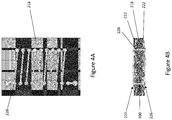
- Figure 4A shows a top-down plan view of an embodiment of an inductor module
- Figure 4B shows a corresponding sectional view.
- Figure 4A shows the inductor module with the ferrite sheet 218 exposed, so that the relationship between the electrically conductive vias 228 and the ferrite sheet 218 is visible in the top-down plan view.
- each individual one of the plurality of electrically conductive vias 228 is disposed in a different through hole 400 formed in the ferrite sheet 218.
- the through holes 400 can be formed by laser drilling, mechanical drilling, stamping, etc. of the ferrite sheet 218.
- Sidewalls of the through holes 400 formed in the ferrite sheet 218 can be covered by an electrically insulating material before the conductive vias 228 are formed, to electrically insulate the vias 228 from the ferrite sheet 218. If the ferrite sheet 218 is not electrically conductive or a poor electrical conductor, the sidewall insulation can be omitted and the vias 228 can be plated directly on the sidewalls of the through holes 400 formed in the ferrite sheet 218. In this case, the ferrite sheet 218 is selected so that the plated metal adheres sufficiently to the sidewalls of the through holes 400 to form the electrically conductive vias 228.
- the holes can have a different size and/or shape than shown e.g. the holes can be larger, have sloped or slanted sidewalls, can be small / round, etc.
- Figure 5A shows a top-down plan view of another embodiment of an inductor module
- Figure 5B shows a corresponding sectional view
- Figure 5A shows the inductor module with the ferrite sheet 218 exposed, so that the relationship between the electrically conductive vias 228 and the ferrite sheet 218 is visible in the top-down plan view.
- the ferrite sheet 218 is pre-formed with a plurality of elongated openings 500 prior to lamination.
- the elongated openings 500 can be formed by laser drilling, mechanical drilling, stamping, etc. of the ferrite sheet 218.
- the PCB insulating material 222 of the inductor module fills the elongated openings 500 during the lamination process.
- Holes are then formed through the PCB insulating material 222 and plated so that a first group 502 of the electrically conductive vias 228 passes through a first preformed elongated opening 500-1 in the ferrite sheet 218 and a second group 504 of the electrically conductive vias 228 passes through a second preformed elongated opening 500-2 in the ferrite sheet 218 to connect the metal traces on both sides of the module and form one or more coils of the inductor.
- the holes can have a different size and/or shape than shown e.g. the holes can be larger, have sloped or slanted sidewalls, can be small / round, etc.
- Figure 6A shows a top-down plan view of an inductor module
- Figure 6B shows a corresponding sectional view.
- Figure 6A shows the inductor module with the ferrite sheet 218 exposed, so that the relationship between the electrically conductive vias 228 and the ferrite sheet 218 is visible in the top-down plan view.
- the ferrite sheet 218 is patterned into an elongated toroid prior to lamination, e.g. by laser drilling, mechanical drilling, stamping, etc.
- the PCB insulating material 222 fills the space around the elongated toroid during the lamination process.
- Holes are then formed through the PCB insulating material 222 and plated so that a first group 600 of the electrically conductive vias 228 extends along a first outer elongated side 602 of the toroid, a second group 604 of the electrically conductive vias 228 extends along a first inner elongated side 606 of the toroid, a third group 608 of the electrically conductive vias 228 extends along a second inner elongated side 610 of the toroid and a fourth group 612 of the electrically conductive vias 228 extends along a second outer elongated side 614 of the toroid to connect the metal traces and form one or more coils of the inductor.
- the holes can have a different size and/or shape than shown e.g. the holes can be larger, have sloped or slanted sidewalls, can be small / round, etc.
- the electrically conductive vias 228 that connect the metal traces to form the inductor coils are plated through holes formed using standard PCB processing.
- the through holes can be lined with an insulating material prior to plating, or be uncovered at the start of the plating process. Depending on the diameter of the through holes, just the sidewalls of the through holes may be plated with the inner part remaining open, or each individual through hole can be filled with metal to form the electrically conductive vias 228.
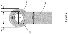
- Figure 7 illustrates an embodiment of one of the electrically conductive vias 228 connected to a metal trace 700 of the inductor module 104.
- the electrically conductive via 228 has a diameter D in a range of 80 micrometers to 300 micrometers, e.g. 100 micrometers to 200 micrometers, 150 micrometers to 200 micrometers, etc.
- the thickness t of the through hole sidewall plating 702 can range from 10 to 15 micrometers to 40 micrometers, for example.
- the width W1 of the metal trace 700 surrounding the electrically conductive via 228 can be in a range of 20 micrometers to 30 micrometers, for example.
- the width W2 of the metal trace 700 elsewhere can be in a range of 200 micrometers to 250 micrometers, for example.
- the dimensions of the metal traces 700 can be smaller or larger, and depend on the target inductance.
- the electrically conductive via 228 can include just the through hole sidewall plating 702, or can be filled entirely with metal.
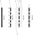
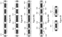
- Figures 8A through 8I illustrate sectional views of an embodiment of manufacturing the inductor modules 104 shown in Figures 1 through 6B .
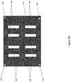
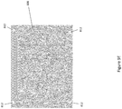
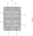
- Figures 9A through 9I illustrate the corresponding top-down plan views.
- a ferrite sheet 218 is provided.
- the dimensions and composition (e.g. NiZn, NiZnCu, MnZn, etc.) of the ferrite sheet 218 can be selected as desired, and depend on the end application.
- the ferrite sheet 218 can have a relative magnetic permeability in a range of 20 Mur to 500 Mur. At higher magnetic fields e.g. H of about 1e4, ferrite sheets with low relative magnetic permeability e.g. less than 100 Mur are well suited for high current applications. At lower magnetic fields e.g. H of about 1e3, ferrite sheets with high relative magnetic permeability e.g. above 200 Mur are well suited for low current applications. Thickness of the ferrite sheet 218 also effects the magnetic performance of the sheet 218.
- elongated openings 500 are formed in the ferrite sheet 218 by laser drilling, mechanical drilling, stamping, etc.
- Alignment holes 800 can also be formed in the ferrite sheet 218 at this step, to aid in the subsequent PCB lamination process.
- a copper sheet (foil) 802 and one or more sheets of PCB insulating material 804 such as prepreg are provided.
- the ferrite sheet 218 is then placed on the one or more sheets of PCB insulating material 804.
- One or more additional sheets of PCB insulating material 806 and another copper sheet (foil) 808 are then placed on the ferrite sheet 218.
- the stack of layers is pressed together and heated to bond the layers together.
- the heat melts and cures epoxy resin in the sheets of PCB insulating material 804, 806 while the pressure bonds the layers together.
- the ferrite sheet 218 with the preformed elongated openings 500 is embedded in the PCB insulating material 804, 806 and the lower and upper copper sheets 802, 808 are laminated onto the insulating material 804, 806 over opposite sides of the ferrite sheet 218 to form a PCB panel 810.
- the elongated openings 500 and alignment holes 800 in the ferrite sheet 218 are illustrated with dashed lines in Figure 9D since the ferrite sheet 218 is out of view.
- the preformed alignment holes 800 are located using e.g. X-ray imaging or by forming openings, and new alignment holes 812 are formed through the PCB panel 810 based on the location of the preformed alignment holes 800 in the ferrite sheet 218.
- the new alignment holes 812 are then used to align the subsequent through hole formation process.
- the new alignment holes 812 can be formed using any standard PCB through hole formation process such as laser or mechanical drilling.
- holes 814 are formed through the upper and lower copper sheets 802, 808 and the PCB insulating material 804, 806.
- the alignment holes 812 formed in Figures 8E and 9E are used to align the through holes 814 with the preformed elongated openings 800 in the ferrite sheet 218.
- the through holes 814 can be formed using any standard PCB through hole formation process such as laser or mechanical drilling.
- the through holes 814 are plated with metal 816.
- Any standard PCB through hole plating process such as electroless deposition, electroplating, direct metallization, etc. can be used to plate the through holes 814 with metal 816.
- the through holes 814 may be completely filled e.g. with Cu.
- the plated holes form electrically conductive vias that extend between the upper and lower copper sheets 802, 808.
- the upper and lower copper sheets 802, 808 are patterned to form metal traces 818 which are electrically connected by the vias 814/816 to form a plurality of individual inductors 820.
- Any standard PCB process for structuring the upper and lower copper sheets 802, 808 can be used such as photolithography and etching, silk screen printing, photoengraving, PCB milling, laser resist ablation, etc.
- the PCB panel 810 is divided into separate PCBs 822.
- Each PCB 822 includes one or more of the individual inductors 820 previously formed in the PCB panel 810.
- Any standard PCB panel singulation process can be used such as drilling or routing perforations along the boundaries of the individual modules, or cutting V-shaped grooves across the full dimension of the PCB panel 810 to form lines of weakness and breaking the panel 810 apart along these lines, laser cutting the PCB panel, mechanical sawing/dicing, etc.
- Figures 10A through 10H illustrate sectional views of another embodiment of manufacturing the inductor modules shown in Figures 1 through 5B .
- Figures 11A through 11H illustrate the corresponding top-down plan views.
- a panel jig 900 with a plurality of alignment pins 902 is provided.
- a copper sheet 904 is placed on the panel jig 900.
- the alignment pins 902 of the panel jig 900 penetrate through the copper sheet 904.
- one or more sheets of PCB insulating material 906 such as prepreg are placed on the copper sheet 904.
- a plurality of separate ferrite sheets 908 are placed on the one or more sheets of PCB insulating material 906.
- the alignment pins 902 of the panel jig 900 are inserted into respective preformed alignment holes 910 of the separate ferrite sheets 908, to align the separate ferrite sheets 908 on the panel jig 900 prior to embedding the separate ferrite sheets 908 in PCB insulating material.
- Each separate ferrite sheet 908 also includes a plurality of elongated openings 912.
- one or more additional sheets of PCB insulating material 914 such as prepreg are placed on the ferrite sheets 908.
- the alignment pins 902 of the panel jig 900 penetrate through each additional sheet of PCB insulating material 914.
- a copper sheet 916 is placed on the one or more additional sheets of PCB insulating material 914.
- the alignment pins 902 of the panel jig 900 penetrate through the top copper sheet 916.
- the PCB layers are point welded 918 to hold the layers in place during the subsequent lamination process.
- the panel jig 900 is removed.
- the panel jig 900 can remain in place during the subsequent lamination process.
- Standard PCB panel lamination and singulation processes are then performed to yield individual inductor modules, e.g. as illustrated in Figures 8D through 9I and described above.
- the holes 920 in the PCB panel that result from removing the alignment pins 902 of the PCB jig 900 can be used to align through holes with the elongated openings 910 in the separate ferrite sheets 908.
- X-ray imaging can be used to detect alignment marks preformed in the ferrite sheets 908. With this approach, exact alignment between the separate ferrite sheets 908 is not necessary. Instead, each ferrite sheet 908 can be aligned separately/i ndividually.
Landscapes
- Engineering & Computer Science (AREA)
- Power Engineering (AREA)
- Manufacturing & Machinery (AREA)
- Microelectronics & Electronic Packaging (AREA)
- Coils Or Transformers For Communication (AREA)
- Semiconductor Integrated Circuits (AREA)
- Dc-Dc Converters (AREA)
Abstract
Description
- The present application relates to inductor modules for power semiconductor systems, in particular an inductor module for attachment to a power stage module of a power semiconductor system.
- DC-DC voltage regulator systems such as buck converters include an arrangement of two power transistors, a gate driver IC and an inductor to convert voltage down for a load. Losses in a real system are generated at the connection path in the power system. To minimize these parasitic losses, the power transistors and the gate driver IC are usually assembled together in a single power module while the inductor is assembled aside on the main PCB (printed circuit board). Losses depend on the distance and cross-section of the connection line between the transistor output (switch node) and the inductor terminals, hence a more ideal solution which positions the inductor closer to the power module is needed.
- According to an embodiment of a power semiconductor system, the power semiconductor system comprises a power stage module comprising one or more power transistor dies attached to or embedded in a first printed circuit board, and an inductor module attached to the power stage module and comprising an inductor electrically connected to an output node of the power stage module, the inductor being formed from a ferrite sheet embedded in a second printed circuit board and windings patterned into the second printed circuit board.
- The inductor module may be soldered to the power stage module or laminated onto the power stage module.
- In some embodiments, the second printed circuit board comprises an insulating material in which the ferrite sheet is embedded, and first and second metal sheets laminated onto the insulating material over opposite sides of the ferrite sheet, and wherein the windings are formed by metal traces patterned into the first and the second metal metals, and a plurality of electrically conductive vias which extend between the first and the second metal sheets and connect the metal traces to form one or more coils.
- In some embodiments, each individual one of the plurality of electrically conductive vias is disposed in a different through hole formed in the ferrite sheet.
- In some embodiments, sidewalls of the through holes formed in the ferrite sheet may be covered by an electrically insulating material.
- The plurality of electrically conductive vias may be electrically insulated from the ferrite sheet.
- In some embodiments, the ferrite sheet has a plurality of elongated openings, and wherein a first group of the plurality of electrically conductive vias passes through a first one of the elongated openings and a second group of the plurality of electrically conductive vias passes through a second one of the elongated openings to connect the metal traces and form the one or more coils.
- In some embodiments, each individual one of the plurality of electrically conductive vias is filled with metal.
- In some embodiments, the ferrite sheet is patterned into an elongated toroid, and wherein a first group of the plurality of electrically conductive vias extends along a first outer elongated side of the toroid, a second group of the plurality of electrically conductive vias extends along a first inner elongated side of the toroid, a third group of the plurality of electrically conductive vias extends along a second inner elongated side of the toroid and a fourth group of the plurality of electrically conductive vias extends along a second outer elongated side of the toroid to connect the metal traces and form the one or more coils.
- In some embodiments, each individual one of the plurality of electrically conductive vias has a diameter in a range of 80 micrometers to 300 micrometers.
- In some embodiments, the power stage module comprises a high-side power transistor and a low-side power transistor of a buck converter coupled at a switching node, and wherein the output node of the power stage module is electrically connected to the switching node.
- In some embodiments, the inductor of the inductor module has an inductance of at least 300 nH.
- According to an embodiment of a method of manufacturing the power semiconductor system, the method comprises: providing a power stage module comprising one or more power transistor dies attached to or embedded in a first printed circuit board; and attaching an inductor module to the power stage module, the inductor module comprising an inductor electrically connected to an output node of the power stage module, the inductor being formed from a ferrite sheet embedded in a second printed circuit board and windings patterned into the second printed circuit board.
- Attaching the inductor module to the power stage module may comprise soldering the inductor module to the power stage module, or laminating the inductor module onto the power stage module.
- According to an embodiment of a method of manufacturing the inductor module, the method comprising: embedding a ferrite sheet in an insulating material, the ferrite sheet having a plurality of elongated openings; laminating first and second metal sheets onto the insulating material over opposite sides of the ferrite sheet to form a panel; forming holes through the first and the second metal sheets and the insulating material, the holes being aligned with the elongated openings in the ferrite sheet; plating the holes with metal to form electrically conductive vias that extend between the first and the second metal sheets; patterning the first and the second metal sheets to form metal traces which are electrically connected by the vias to form a plurality of individual inductors; and dividing the panel into separate printed circuit boards, each printed circuit board including one or more of the individual inductors.
- In some embodiments, a plurality of separate ferrite sheets each with a plurality of elongated openings is embedded in the insulating material.
- In some embodiments, the method further comprises inserting pins of a panel jig into respective alignment holes of the separate ferrite sheets, to align the plurality of separate ferrite sheets on the panel jig prior to embedding the separate ferrite sheets in the insulating material.
- In some embodiments, the method further comprises using preformed alignment holes in the ferrite sheet to align forming the holes through the first and the second metal sheets and the insulating material with the elongated openings in the ferrite sheet.
- In some embodiments, using the preformed alignment holes in the ferrite sheet to align forming the holes formed through the first and the second metal sheets and the insulating material with the elongated openings in the ferrite sheet comprises locating the preformed alignment holes, forming new alignment holes through the first and the second metal sheets, the ferrite sheet and the insulating material based on the location of the preformed alignment holes in the ferrite sheet, and using the new alignment holes to align forming the holes through the first and the second metal sheets and the insulating material with the elongated openings in the ferrite sheet.
- Those skilled in the art will recognize additional features and advantages upon reading the following detailed description, and upon viewing the accompanying drawings.
- The elements of the drawings are not necessarily to scale relative to each other. Like reference numerals designate corresponding similar parts. The features of the various illustrated embodiments can be combined unless they exclude each other. Embodiments are depicted in the drawings and are detailed in the description which follows.
-
Figure 1 illustrates a schematic view of an embodiment of a power semiconductor system that includes an inductor module attached to a power stage module. -
Figure 2 illustrates a sectional view of an embodiment of a plurality of individual inductor modules soldered to a PCB panel of power stage modules. -
Figure 3A illustrates a sectional view of an embodiment of a PCB panel of inductor modules laminated onto a PCB panel of power stage modules. -
Figure 3B illustrates a sectional view of another embodiment of a PCB panel of inductor modules laminated onto a PCB panel of power stage modules. -
Figure 4A illustrates a top-down plan view of an embodiment of an inductor module, andFigure 4B illustrates a corresponding sectional view of the inductor module. -
Figure 5A illustrates a top-down plan view of another embodiment of an inductor module, andFigure 5B illustrates a corresponding sectional view of the inductor module. -
Figure 6A illustrates a top-down plan view of yet another embodiment of an inductor module, andFigure 6B illustrates a corresponding sectional view of the inductor module. -
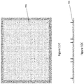
Figure 7 illustrates a top-down plan view of an embodiment of an electronically conductive via and metal trace of an inductor module. -
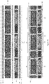
Figures 8A through 8I illustrate sectional views of an embodiment of manufacturing the inductor modules shown inFigures 1 through 6B , andFigures 9A through 9I illustrate corresponding top-down plan views. -
Figures 10A through 10H illustrate sectional views of another embodiment of manufacturing the inductor modules shown inFigures 1 through 6B , andFigures 11A through 11H illustrate corresponding top-down plan views. - The embodiments described herein provide embedded PCB inductor modules manufactured using standard PCB processes with PCB materials and ferrite sheets. The inductor modules can be mounted on top of power stage modules of a DC-DC converter, using standard soldering or lamination and via drilling processes. The size and shape of the inductor modules can be optimized to match the power stage module to which the inductor module is to be attached. With such an inductor module, overall system cost and size is reduced while allowing for the manufacture of a customized (size, shape, inductance / resistance value, etc.) inductor module for various applications.
- The inductor modules include an embedded ferrite sheet and metal wiring on both sides of the module connected together by plated through holes. The inductor module can be integrated into a power stage or other module with embedded die(s) using soldering or lamination processes. The ferrite sheet is used as an inductor core layer in a standard PCB board. The ferrite sheet is embedded in a standard PCB insulating material such as FR4, prepreg (sheets of glass cloth preimpregnated with uncured epoxy resin), resin sheets, epoxy, etc., and metal sheets are laminated onto the insulating material using standard PCB processes. The inductor wiring is implemented by traces pattered into the metal sheets on the top and bottom sides of the inductor module that are connected together by plated through holes. The ferrite sheet can include elongated openings for the plated through holes. The cross-section area through which the flux passes can be made very wide. Due to the absence of an air gap, the flux is confined in the magnetic core (ferrite sheet), which reduces fringing effects and lowers EMI (electromagnetic interference), and depending on the properties of the ferrite sheet, allows the core to saturate easier at high current.
-
Figure 1 illustrates an embodiment of a DC-DC voltage regulator system of the buck converter type. The buck converter system includes high-side and low-side power transistors M1, M2 such as power MOSFETs (metal-oxide-semiconductor field effect transistors), IGBTs (insulated gate bipolar transistors), HEMTs (high electron mobility transistors), etc., a gate driver IC (integrated circuit) 100, and an inductor L and capacitor C to convert an input voltage Vin down to Vout for a load which is represented by resistor R. The high-side power transistor M1 and the low-side power transistor M2 are coupled at a switching node Vsw. The inductor L is coupled to the switching node Vsw, and the capacitor C is coupled to the inductor L for reducing voltage ripple at the regulator output Vout. Losses in such a system are generated at the connection paths in the power system, e.g. between the switch node Vsw of the converter and the output inductor L. To minimize parasitic losses, the power transistors M1, M2 and the gate driver IC 100 are assembled together in asingle package 102, also referred to herein as a power stage module. The inductor L is assembled in aseparate module 104 using standard PCB processes, and attached to the output OUT of thepower stage module 102 e.g. by soldering or lamination. The output OUT of thepower stage module 102 is electrically connected internally to the switch node Vsw. In one embodiment, the inductor L of theinductor module 104 attached to thepower stage module 102 has an inductance in a range of 400 nH to 550 nH, a resistance less than 100 milliohm and a saturation current of about 8 A or greater. In general, the inductors are well-suited for power applications and designed for high-current such as 1 or more amperes. For high-power applications, the inductance is at least 300 nH or greater to avoid saturation. -
Figure 2 illustrates an embodiment of attachingseparate inductor modules 102 to aPCB panel 200 ofpower stage modules 102 to form power semiconductor systems. According to this embodiment, there are multiplepower stage modules 102 in thePCB panel 200 and thepower stage modules 102 have yet to be singulated at the time of inductor module attachment. Theindividual inductor modules 104, having already been manufactured and singulated, are soldered to respective ones of thepower stage modules 102. Any standard soldering process can be used to formsolder joints 202 between thepower stage modules 102 and therespective inductor modules 102. - Both the
power stage modules 102 and theseparate inductor modules 104 are formed using standard PCB processing according to the embodiment shown inFigure 2 . Eachpower stage module 102 includes one or more power transistor dies 204 attached to or embedded in afirst PCB 206. Thefirst PCB 206 includes one or morepatterned metal sheets 208 laminated on standardPCB insulating material 210 such as FR4, prepreg, resin sheets, epoxy, etc. Conductive vias 212 form electrical connections between thepatterned metal sheets 208 and between apatterned metal sheet 208 and the die(s) 204 included in the respectivepower stage modules 102. Contactpads 216 can be patterned into the topmost and bottommost metal sheets of thepower stage modules 102, to provide electrical and/or thermal pathways to eachpower stage module 102. Some of the top-side contact pads 216 of thepower stage modules 102 inFigure 2 form the output node OUT shown inFigure 1 . - Each
inductor module 104 comprises an inductor electrically connected to the output node of thepower stage module 102 to which thatinductor module 104 is soldered. The inductor is formed from aferrite sheet 218 embedded in asecond PCB board 220 and windings patterned into thesecond PCB 220. Thesecond PCB 220 includes a standardPCB insulating material 222 such as FR4, prepreg, resin sheets, epoxy, etc. in which theferrite sheet 218 is embedded. First andsecond metal sheets material 222 over opposite sides of theferrite sheet 218 using standard PCB processing. The inductor windings are formed by metal traces patterned into themetal sheets conductive vias 228 which extend between themetal sheets inductor modules 104 to the respectivepower stage modules 102 of thePCB panel 200, individual power semiconductor systems can be realized by singulating thePCB panel 200 e.g. by sawing, dicing, etc. -
Figure 3A illustrates another embodiment of attachinginductor modules 104 topower stage modules 102 to form power semiconductor systems. The embodiment shown inFigure 3A is similar to the embodiment shown inFigure 2 . Different, however, theinductor modules 104 are laminated onto the respectivepower stage modules 102. According to this embodiment, both thepower stage modules 102 and theinductor modules 104 are still arranged as part ofdifferent PCB panels inductor modules 104 nor thepower stage modules 102 are singulated prior to attachment. Standard PCB processing is employed to form an additional insulatingmaterial 302 such as FR4, prepreg, resin sheets, epoxy, etc. between the powerstage PCB panel 200 and theinductor PCB panel 300. Electricallyconductive vias 304 are formed in the additionalPCB insulating material 302 to electrically connect the inductors of theinductor modules 104 to the respective output nodes of thepower stage modules 102. After lamination of theinductor PCB panel 300 to the powerstage PCB panel 200, individual power semiconductor systems can be realized by singulation, e.g. by sawing, dicing, etc. -
Figure 3B illustrates another embodiment of attaching theinductor modules 104 to thepower stage modules 102 by a lamination process to form power semiconductor systems. According to this embodiment, theinductor PCB panel 300 is laminated to the powerstage PCB panel 200 by aligning thepanels PCB insulating materials metal sheets bottom metal sheets bottom contact pads connections 320 to thebottom contact pads 318, and through viaconnections 322 to electrically connect therespective inductor modules 104 to the correspondingpower stage modules 102. After lamination of theinductor PCB panel 300 to the powerstage PCB panel 200, individual power semiconductor systems can be realized by singulation, e.g. by sawing, dicing, etc. - Various embodiments of inductor module structures and methods of manufacture are described next.
-
Figure 4A shows a top-down plan view of an embodiment of an inductor module, andFigure 4B shows a corresponding sectional view.Figure 4A shows the inductor module with theferrite sheet 218 exposed, so that the relationship between the electricallyconductive vias 228 and theferrite sheet 218 is visible in the top-down plan view. According to this embodiment, each individual one of the plurality of electricallyconductive vias 228 is disposed in a different throughhole 400 formed in theferrite sheet 218. The throughholes 400 can be formed by laser drilling, mechanical drilling, stamping, etc. of theferrite sheet 218. Sidewalls of the throughholes 400 formed in theferrite sheet 218 can be covered by an electrically insulating material before theconductive vias 228 are formed, to electrically insulate thevias 228 from theferrite sheet 218. If theferrite sheet 218 is not electrically conductive or a poor electrical conductor, the sidewall insulation can be omitted and thevias 228 can be plated directly on the sidewalls of the throughholes 400 formed in theferrite sheet 218. In this case, theferrite sheet 218 is selected so that the plated metal adheres sufficiently to the sidewalls of the throughholes 400 to form the electricallyconductive vias 228. The holes can have a different size and/or shape than shown e.g. the holes can be larger, have sloped or slanted sidewalls, can be small / round, etc. -
Figure 5A shows a top-down plan view of another embodiment of an inductor module, andFigure 5B shows a corresponding sectional view.Figure 5A shows the inductor module with theferrite sheet 218 exposed, so that the relationship between the electricallyconductive vias 228 and theferrite sheet 218 is visible in the top-down plan view. According to this embodiment, theferrite sheet 218 is pre-formed with a plurality ofelongated openings 500 prior to lamination. Theelongated openings 500 can be formed by laser drilling, mechanical drilling, stamping, etc. of theferrite sheet 218. ThePCB insulating material 222 of the inductor module fills theelongated openings 500 during the lamination process. Holes are then formed through thePCB insulating material 222 and plated so that afirst group 502 of the electricallyconductive vias 228 passes through a first preformed elongated opening 500-1 in theferrite sheet 218 and asecond group 504 of the electricallyconductive vias 228 passes through a second preformed elongated opening 500-2 in theferrite sheet 218 to connect the metal traces on both sides of the module and form one or more coils of the inductor. The holes can have a different size and/or shape than shown e.g. the holes can be larger, have sloped or slanted sidewalls, can be small / round, etc. -
Figure 6A shows a top-down plan view of an inductor module, andFigure 6B shows a corresponding sectional view.Figure 6A shows the inductor module with theferrite sheet 218 exposed, so that the relationship between the electricallyconductive vias 228 and theferrite sheet 218 is visible in the top-down plan view. According to this embodiment, theferrite sheet 218 is patterned into an elongated toroid prior to lamination, e.g. by laser drilling, mechanical drilling, stamping, etc. ThePCB insulating material 222 fills the space around the elongated toroid during the lamination process. Holes are then formed through thePCB insulating material 222 and plated so that afirst group 600 of the electricallyconductive vias 228 extends along a first outerelongated side 602 of the toroid, asecond group 604 of the electricallyconductive vias 228 extends along a first innerelongated side 606 of the toroid, athird group 608 of the electricallyconductive vias 228 extends along a second innerelongated side 610 of the toroid and afourth group 612 of the electricallyconductive vias 228 extends along a second outerelongated side 614 of the toroid to connect the metal traces and form one or more coils of the inductor. The holes can have a different size and/or shape than shown e.g. the holes can be larger, have sloped or slanted sidewalls, can be small / round, etc. - In each of the embodiments illustrated in
Figures 1 through 6B , the electricallyconductive vias 228 that connect the metal traces to form the inductor coils are plated through holes formed using standard PCB processing. The through holes can be lined with an insulating material prior to plating, or be uncovered at the start of the plating process. Depending on the diameter of the through holes, just the sidewalls of the through holes may be plated with the inner part remaining open, or each individual through hole can be filled with metal to form the electricallyconductive vias 228. -
Figure 7 illustrates an embodiment of one of the electricallyconductive vias 228 connected to ametal trace 700 of theinductor module 104. According to this embodiment, the electrically conductive via 228 has a diameter D in a range of 80 micrometers to 300 micrometers, e.g. 100 micrometers to 200 micrometers, 150 micrometers to 200 micrometers, etc. The thickness t of the through hole sidewall plating 702 can range from 10 to 15 micrometers to 40 micrometers, for example. The width W1 of themetal trace 700 surrounding the electrically conductive via 228 can be in a range of 20 micrometers to 30 micrometers, for example. The width W2 of themetal trace 700 elsewhere can be in a range of 200 micrometers to 250 micrometers, for example. The dimensions of the metal traces 700 can be smaller or larger, and depend on the target inductance. The electrically conductive via 228 can include just the through hole sidewall plating 702, or can be filled entirely with metal. -
Figures 8A through 8I illustrate sectional views of an embodiment of manufacturing theinductor modules 104 shown inFigures 1 through 6B .Figures 9A through 9I illustrate the corresponding top-down plan views. - In
Figures 8A and9A , aferrite sheet 218 is provided. The dimensions and composition (e.g. NiZn, NiZnCu, MnZn, etc.) of theferrite sheet 218 can be selected as desired, and depend on the end application. For example, theferrite sheet 218 can have a relative magnetic permeability in a range of 20 Mur to 500 Mur. At higher magnetic fields e.g. H of about 1e4, ferrite sheets with low relative magnetic permeability e.g. less than 100 Mur are well suited for high current applications. At lower magnetic fields e.g. H of about 1e3, ferrite sheets with high relative magnetic permeability e.g. above 200 Mur are well suited for low current applications. Thickness of theferrite sheet 218 also effects the magnetic performance of thesheet 218. - In
Figures 8B and9B ,elongated openings 500 are formed in theferrite sheet 218 by laser drilling, mechanical drilling, stamping, etc. Alignment holes 800 can also be formed in theferrite sheet 218 at this step, to aid in the subsequent PCB lamination process. - In
Figures 8C and9C , a copper sheet (foil) 802 and one or more sheets ofPCB insulating material 804 such as prepreg are provided. Theferrite sheet 218 is then placed on the one or more sheets ofPCB insulating material 804. One or more additional sheets ofPCB insulating material 806 and another copper sheet (foil) 808 are then placed on theferrite sheet 218. - In
Figures 8D and9D , the stack of layers is pressed together and heated to bond the layers together. The heat melts and cures epoxy resin in the sheets ofPCB insulating material ferrite sheet 218 with the preformedelongated openings 500 is embedded in thePCB insulating material upper copper sheets material ferrite sheet 218 to form aPCB panel 810. Theelongated openings 500 andalignment holes 800 in theferrite sheet 218 are illustrated with dashed lines inFigure 9D since theferrite sheet 218 is out of view. - In
Figures 8E and9E , the preformedalignment holes 800 are located using e.g. X-ray imaging or by forming openings, and new alignment holes 812 are formed through thePCB panel 810 based on the location of the preformedalignment holes 800 in theferrite sheet 218. The new alignment holes 812 are then used to align the subsequent through hole formation process. The new alignment holes 812 can be formed using any standard PCB through hole formation process such as laser or mechanical drilling. - In
Figures 8F and9F , holes 814 are formed through the upper andlower copper sheets PCB insulating material Figures 8E and9E are used to align the throughholes 814 with the preformedelongated openings 800 in theferrite sheet 218. The throughholes 814 can be formed using any standard PCB through hole formation process such as laser or mechanical drilling. - In
Figures 8G and9G , the throughholes 814 are plated withmetal 816. Any standard PCB through hole plating process such as electroless deposition, electroplating, direct metallization, etc. can be used to plate the throughholes 814 withmetal 816. As explained above, depending on the diameter of the throughholes 814, only sidewalls of the throughholes 814 may be plated or the throughholes 814 may be completely filled e.g. with Cu. The plated holes form electrically conductive vias that extend between the upper andlower copper sheets - In
Figures 8H and9H , the upper andlower copper sheets vias 814/816 to form a plurality ofindividual inductors 820. Any standard PCB process for structuring the upper andlower copper sheets - In
Figures 8I and9I , thePCB panel 810 is divided intoseparate PCBs 822. EachPCB 822 includes one or more of theindividual inductors 820 previously formed in thePCB panel 810. Any standard PCB panel singulation process can be used such as drilling or routing perforations along the boundaries of the individual modules, or cutting V-shaped grooves across the full dimension of thePCB panel 810 to form lines of weakness and breaking thepanel 810 apart along these lines, laser cutting the PCB panel, mechanical sawing/dicing, etc. -
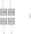
Figures 10A through 10H illustrate sectional views of another embodiment of manufacturing the inductor modules shown inFigures 1 through 5B .Figures 11A through 11H illustrate the corresponding top-down plan views. - In
Figures 10A and 11A , apanel jig 900 with a plurality of alignment pins 902 is provided. - In
Figures 10B and 11B , acopper sheet 904 is placed on thepanel jig 900. The alignment pins 902 of thepanel jig 900 penetrate through thecopper sheet 904. - In
Figures 10C and 11C , one or more sheets ofPCB insulating material 906 such as prepreg are placed on thecopper sheet 904. The alignment pins 902 of thepanel jig 900 penetrate through each sheet ofPCB insulating material 906. - In
Figures 10D and 11D , a plurality ofseparate ferrite sheets 908 are placed on the one or more sheets ofPCB insulating material 906. The alignment pins 902 of thepanel jig 900 are inserted into respective preformedalignment holes 910 of theseparate ferrite sheets 908, to align theseparate ferrite sheets 908 on thepanel jig 900 prior to embedding theseparate ferrite sheets 908 in PCB insulating material. Eachseparate ferrite sheet 908 also includes a plurality ofelongated openings 912. - In
Figures 10E and 11E , one or more additional sheets ofPCB insulating material 914 such as prepreg are placed on theferrite sheets 908. The alignment pins 902 of thepanel jig 900 penetrate through each additional sheet ofPCB insulating material 914. - In
Figures 10F and 11F , acopper sheet 916 is placed on the one or more additional sheets ofPCB insulating material 914. The alignment pins 902 of thepanel jig 900 penetrate through thetop copper sheet 916. - In
Figures 10G and 11G , the PCB layers are point welded 918 to hold the layers in place during the subsequent lamination process. - In
Figures 10H and 11H , thepanel jig 900 is removed. Alternatively, thepanel jig 900 can remain in place during the subsequent lamination process. Standard PCB panel lamination and singulation processes are then performed to yield individual inductor modules, e.g. as illustrated inFigures 8D through 9I and described above. The holes 920 in the PCB panel that result from removing the alignment pins 902 of thePCB jig 900 can be used to align through holes with theelongated openings 910 in theseparate ferrite sheets 908. In another embodiment, X-ray imaging can be used to detect alignment marks preformed in theferrite sheets 908. With this approach, exact alignment between theseparate ferrite sheets 908 is not necessary. Instead, eachferrite sheet 908 can be aligned separately/i ndividually. - Terms such as "first", "second", and the like, are used to describe various elements, regions, sections, etc. and are also not intended to be limiting. Like terms refer to like elements throughout the description.
- As used herein, the terms "having", "containing", "including", "comprising" and the like are open ended terms that indicate the presence of stated elements or features, but do not preclude additional elements or features. The articles "a", "an" and "the" are intended to include the plural as well as the singular, unless the context clearly indicates otherwise.
- It is to be understood that the features of the various embodiments described herein may be combined with each other, unless specifically noted otherwise.
- Although specific embodiments have been illustrated and described herein, it will be appreciated by those of ordinary skill in the art that a variety of alternate and/or equivalent implementations may be substituted for the specific embodiments shown and described without departing from the scope of the present invention. This application is intended to cover any adaptations or variations of the specific embodiments discussed herein. Therefore, it is intended that this invention be limited only by the claims and the equivalents thereof.
Claims (15)
- A power semiconductor system, comprising:a power stage module comprising one or more power transistor dies attached to or embedded in a first printed circuit board; andan inductor module attached to the power stage module and comprising an inductor electrically connected to an output node of the power stage module, the inductor being formed from a ferrite sheet embedded in a second printed circuit board and windings patterned into the second printed circuit board.
- The power semiconductor system of claim 1, wherein the inductor module is soldered to the power stage module, or is laminated onto the power stage module.
- The power semiconductor system of claim 1 or claim 2, wherein the second printed circuit board comprises an insulating material in which the ferrite sheet is embedded, and first and second metal sheets laminated onto the insulating material over opposite sides of the ferrite sheet, and wherein the windings are formed by metal traces patterned into the first and the second metal metals, and a plurality of electrically conductive vias which extend between the first and the second metal sheets and connect the metal traces to form one or more coils.
- The power semiconductor system of claim 3, wherein each individual one of the plurality of electrically conductive vias is disposed in a different through hole formed in the ferrite sheet.
- The power semiconductor system of claim 4, wherein sidewalls of the through holes formed in the ferrite sheet are covered by an electrically insulating material.
- The power semiconductor system of claim 3, wherein the ferrite sheet has a plurality of elongated openings, and wherein a first group of the plurality of electrically conductive vias passes through a first one of the elongated openings and a second group of the plurality of electrically conductive vias passes through a second one of the elongated openings to connect the metal traces and form the one or more coils.
- The power semiconductor system of any one of claims 3 to 6, wherein the plurality of electrically conductive vias is electrically insulated from the ferrite sheet.
- The power semiconductor system of any one of claims 3 to 7, wherein the ferrite sheet is patterned into an elongated toroid, and wherein a first group of the plurality of electrically conductive vias extends along a first outer elongated side of the toroid, a second group of the plurality of electrically conductive vias extends along a first inner elongated side of the toroid, a third group of the plurality of electrically conductive vias extends along a second inner elongated side of the toroid and a fourth group of the plurality of electrically conductive vias extends along a second outer elongated side of the toroid to connect the metal traces and form the one or more coils.
- The power semiconductor system of any one of claims 1 to 8, wherein the power stage module comprises a high-side power transistor and a low-side power transistor of a buck converter coupled at a switching node, and wherein the output node of the power stage module is electrically connected to the switching node.
- A method of manufacturing a power semiconductor system, the method comprising:providing a power stage module comprising one or more power transistor dies attached to or embedded in a first printed circuit board; andattaching an inductor module to the power stage module, the inductor module comprising an inductor electrically connected to an output node of the power stage module, the inductor being formed from a ferrite sheet embedded in a second printed circuit board and windings patterned into the second printed circuit board.
- The method of claim 10, wherein attaching the inductor module to the power stage module comprises soldering the inductor module to the power stage module, or laminating the inductor module onto the power stage module.
- A method of manufacturing inductor modules, the method comprising:embedding a ferrite sheet in an insulating material, the ferrite sheet having a plurality of elongated openings;laminating first and second metal sheets onto the insulating material over opposite sides of the ferrite sheet to form a panel;forming holes through the first and the second metal sheets and the insulating material, the holes being aligned with the elongated openings in the ferrite sheet;plating the holes with metal to form electrically conductive vias that extend between the first and the second metal sheets;patterning the first and the second metal sheets to form metal traces which are electrically connected by the vias to form a plurality of individual inductors; anddividing the panel into separate printed circuit boards, each printed circuit board including one or more of the individual inductors.
- The method of claim 12, wherein a plurality of separate ferrite sheets each with a plurality of elongated openings is embedded in the insulating material, the method further comprising:inserting pins of a panel jig into respective alignment holes of the separate ferrite sheets, to align the plurality of separate ferrite sheets on the panel jig prior to embedding the separate ferrite sheets in the insulating material.
- The method of claim 12 or claim 13, further comprising:using preformed alignment holes in the ferrite sheet to align forming the holes through the first and the second metal sheets and the insulating material with the elongated openings in the ferrite sheet.
- The method of claim 14, wherein using the preformed alignment holes in the ferrite sheet to align forming the holes formed through the first and the second metal sheets and the insulating material with the elongated openings in the ferrite sheet comprises:locating the preformed alignment holes;forming new alignment holes through the first and the second metal sheets, the ferrite sheet and the insulating material based on the location of the preformed alignment holes in the ferrite sheet; andusing the new alignment holes to align forming the holes through the first and the second metal sheets and the insulating material with the elongated openings in the ferrite sheet.
Applications Claiming Priority (1)
| Application Number | Priority Date | Filing Date | Title |
|---|---|---|---|
| US15/699,740 US10601314B2 (en) | 2017-09-08 | 2017-09-08 | Power semiconductor systems having inductor modules, and methods of manufacturing inductor modules and power semiconductor systems having inductor modules |
Publications (3)
| Publication Number | Publication Date |
|---|---|
| EP3454350A2 true EP3454350A2 (en) | 2019-03-13 |
| EP3454350A3 EP3454350A3 (en) | 2019-05-22 |
| EP3454350B1 EP3454350B1 (en) | 2021-11-03 |
Family
ID=63517708
Family Applications (1)
| Application Number | Title | Priority Date | Filing Date |
|---|---|---|---|
| EP18192632.0A Active EP3454350B1 (en) | 2017-09-08 | 2018-09-05 | Power semiconductor systems having inductor modules, and methods of manufacturing inductor modules and power semiconductor systems having inductor modules |
Country Status (3)
| Country | Link |
|---|---|
| US (4) | US10601314B2 (en) |
| EP (1) | EP3454350B1 (en) |
| CN (2) | CN117914129A (en) |
Cited By (1)
| Publication number | Priority date | Publication date | Assignee | Title |
|---|---|---|---|---|
| CN113224949A (en) * | 2020-02-04 | 2021-08-06 | 英飞凌科技奥地利有限公司 | Power module and electronic system |
Families Citing this family (6)
| Publication number | Priority date | Publication date | Assignee | Title |
|---|---|---|---|---|
| US11451093B2 (en) * | 2017-09-05 | 2022-09-20 | University Of Florida Research Foundation, Incorporated | Wireless power transfer to biomedical implants |
| JP6498809B1 (en) * | 2018-03-08 | 2019-04-10 | 日本航空電子工業株式会社 | Electrical connector |
| US11050355B2 (en) | 2019-10-17 | 2021-06-29 | Infineon Technologies Austria Ag | Stacked power supply topologies and inductor devices |
| DE102020127327B4 (en) * | 2020-10-16 | 2025-07-03 | Infineon Technologies Ag | Stacked transistor chip package with source coupling |
| EP4092740B1 (en) * | 2021-05-21 | 2025-06-25 | Infineon Technologies Austria AG | Semiconductor die with a vertical transistor device |
| US20250095902A1 (en) | 2023-09-19 | 2025-03-20 | Monolithic Power Systems, Inc. | Inductor assembly and power module using the same |
Family Cites Families (19)
| Publication number | Priority date | Publication date | Assignee | Title |
|---|---|---|---|---|
| US3858138A (en) * | 1973-03-05 | 1974-12-31 | Rca Corp | Tuneable thin film inductor |
| KR100250225B1 (en) * | 1996-11-19 | 2000-04-01 | 윤종용 | Integrated circuit inductor and manufacturing method |
| US7786837B2 (en) * | 2007-06-12 | 2010-08-31 | Alpha And Omega Semiconductor Incorporated | Semiconductor power device having a stacked discrete inductor structure |
| US8217748B2 (en) | 2007-11-23 | 2012-07-10 | Alpha & Omega Semiconductor Inc. | Compact inductive power electronics package |
| US8344842B1 (en) * | 2010-01-20 | 2013-01-01 | Vlt, Inc. | Vertical PCB surface mount inductors and power converters |
| US8325002B2 (en) * | 2010-05-27 | 2012-12-04 | Advanced Semiconductor Engineering, Inc. | Power inductor structure |
| JP2012156184A (en) * | 2011-01-24 | 2012-08-16 | Nec Corp | Mounting board and method of manufacturing the same |
| US20120299150A1 (en) * | 2011-05-26 | 2012-11-29 | Primarion, Inc. | Power Semiconductor Module with Embedded Chip Package |
| JP5713148B2 (en) * | 2013-01-24 | 2015-05-07 | 株式会社村田製作所 | Manufacturing method of resin multilayer substrate with built-in magnetic core |
| US9936579B2 (en) * | 2013-02-01 | 2018-04-03 | Apple Inc. | Low profile packaging and assembly of a power conversion system in modular form |
| JP6139329B2 (en) * | 2013-08-16 | 2017-05-31 | 日本碍子株式会社 | Ceramic circuit board and electronic device |
| US9564264B2 (en) * | 2013-08-30 | 2017-02-07 | Virginia Tech Intellectual Properties, Inc. | High frequency integrated point-of-load power converter with embedded inductor substrate |
| US10109404B2 (en) | 2013-08-30 | 2018-10-23 | Virginia Tech Intellectual Properties, Inc. | Low profile coupled inductor substrate with transient speed improvement |
| KR20150066184A (en) * | 2013-12-06 | 2015-06-16 | 삼성전자주식회사 | Semiconductor package and method of manufacturing the same |
| GB2531354B (en) * | 2014-10-17 | 2018-01-10 | Murata Manufacturing Co | An embedded magnetic component Device |
| US9912058B2 (en) | 2014-10-21 | 2018-03-06 | Infineon Technologies Ag | Hybrid antenna, antenna arrangement and method for manufacturing an antenna arrangement |
| WO2016076121A1 (en) | 2014-11-12 | 2016-05-19 | 株式会社村田製作所 | Power supply module and mounting structure thereof |
| US9685880B2 (en) * | 2015-09-28 | 2017-06-20 | Apple Inc. | Power converters |
| DE102016105096B4 (en) | 2016-03-18 | 2021-05-27 | Infineon Technologies Ag | SEMICONDUCTOR DEVICE WITH A PASSIVE COMPONENT FORMED IN A REDISTRIBUTION LAYER |
-
2017
- 2017-09-08 US US15/699,740 patent/US10601314B2/en active Active
-
2018
- 2018-09-05 EP EP18192632.0A patent/EP3454350B1/en active Active
- 2018-09-07 CN CN202410098163.1A patent/CN117914129A/en active Pending
- 2018-09-07 CN CN201811044846.XA patent/CN109474174A/en active Pending
-
2020
- 2020-03-06 US US16/811,853 patent/US10833583B2/en active Active
- 2020-10-20 US US17/074,759 patent/US11539291B2/en active Active
-
2022
- 2022-12-22 US US18/086,736 patent/US11996771B2/en active Active
Non-Patent Citations (1)
| Title |
|---|
| None |
Cited By (1)
| Publication number | Priority date | Publication date | Assignee | Title |
|---|---|---|---|---|
| CN113224949A (en) * | 2020-02-04 | 2021-08-06 | 英飞凌科技奥地利有限公司 | Power module and electronic system |
Also Published As
| Publication number | Publication date |
|---|---|
| US11539291B2 (en) | 2022-12-27 |
| US10601314B2 (en) | 2020-03-24 |
| EP3454350B1 (en) | 2021-11-03 |
| US10833583B2 (en) | 2020-11-10 |
| US20200212798A1 (en) | 2020-07-02 |
| EP3454350A3 (en) | 2019-05-22 |
| CN109474174A (en) | 2019-03-15 |
| US20210036610A1 (en) | 2021-02-04 |
| CN117914129A (en) | 2024-04-19 |
| US11996771B2 (en) | 2024-05-28 |
| US20190081562A1 (en) | 2019-03-14 |
| US20230127874A1 (en) | 2023-04-27 |
Similar Documents
| Publication | Publication Date | Title |
|---|---|---|
| US11996771B2 (en) | Power semiconductor system having an inductor module attached to a power stage module | |
| US7868431B2 (en) | Compact power semiconductor package and method with stacked inductor and integrated circuit die | |
| US7843303B2 (en) | Multilayer inductor | |
| US11948721B2 (en) | Packaged isolation barrier with integrated magnetics | |
| TWI385766B (en) | Small power semiconductor package with stacked inductor and integrated circuit chip and production method thereof | |
| US20090194857A1 (en) | Thin Compact Semiconductor Die Packages Suitable for Smart-Power Modules, Methods of Making the Same, and Systems Using the Same | |
| US20170025379A1 (en) | Power module package | |
| JP2020053593A (en) | Substrate with built-in mos transistor and switching power supply using the same | |
| KR20000029817A (en) | Planar transformer | |
| CN114446591A (en) | Voltage regulation module | |
| US11778746B2 (en) | Assembly structure of transformer and circuit board as well as assembly method thereof | |
| US11152340B2 (en) | Power module having a multilayered structure with liquid cooled busbar and method for manufacturing same | |
| CN101964249A (en) | Power inductor structure | |
| CN111564956B (en) | Power stage device with carrier frame for power stage modules and integrated inductor | |
| WO2004040599A1 (en) | A circuit board with a planar magnetic element | |
| US20160380538A1 (en) | Current Distribution in DC-DC Converters | |
| US20260123408A1 (en) | Electronic device cooling with integrated magnetics | |
| KR20180002363A (en) | Snubber Circuit Integrated Planar Transformer | |
| US20260005133A1 (en) | Integrated mmc package with inductor and die | |
| RU2746054C1 (en) | Method for producing a planar transformer based on multi-layer pcb | |
| US20250372509A1 (en) | Microelectronic device package with hybrid isolation laminate | |
| JP2010034310A (en) | Transformer and power converter | |
| JP2006073868A (en) | Manufacturing method of micro power converter |
Legal Events
| Date | Code | Title | Description |
|---|---|---|---|
| PUAI | Public reference made under article 153(3) epc to a published international application that has entered the european phase |
Free format text: ORIGINAL CODE: 0009012 |
|
| STAA | Information on the status of an ep patent application or granted ep patent |
Free format text: STATUS: THE APPLICATION HAS BEEN PUBLISHED |
|
| AK | Designated contracting states |
Kind code of ref document: A2 Designated state(s): AL AT BE BG CH CY CZ DE DK EE ES FI FR GB GR HR HU IE IS IT LI LT LU LV MC MK MT NL NO PL PT RO RS SE SI SK SM TR |
|
| AX | Request for extension of the european patent |
Extension state: BA ME |
|
| PUAL | Search report despatched |
Free format text: ORIGINAL CODE: 0009013 |
|
| AK | Designated contracting states |
Kind code of ref document: A3 Designated state(s): AL AT BE BG CH CY CZ DE DK EE ES FI FR GB GR HR HU IE IS IT LI LT LU LV MC MK MT NL NO PL PT RO RS SE SI SK SM TR |
|
| AX | Request for extension of the european patent |
Extension state: BA ME |
|
| RIC1 | Information provided on ipc code assigned before grant |
Ipc: H01F 27/06 20060101ALI20190412BHEP Ipc: H01F 27/255 20060101ALI20190412BHEP Ipc: H01F 41/04 20060101ALI20190412BHEP Ipc: H01F 17/00 20060101AFI20190412BHEP Ipc: H01F 17/06 20060101ALI20190412BHEP |
|
| STAA | Information on the status of an ep patent application or granted ep patent |
Free format text: STATUS: REQUEST FOR EXAMINATION WAS MADE |
|
| 17P | Request for examination filed |
Effective date: 20191122 |
|
| RBV | Designated contracting states (corrected) |
Designated state(s): AL AT BE BG CH CY CZ DE DK EE ES FI FR GB GR HR HU IE IS IT LI LT LU LV MC MK MT NL NO PL PT RO RS SE SI SK SM TR |
|
| STAA | Information on the status of an ep patent application or granted ep patent |
Free format text: STATUS: EXAMINATION IS IN PROGRESS |
|
| 17Q | First examination report despatched |
Effective date: 20200309 |
|
| RIC1 | Information provided on ipc code assigned before grant |
Ipc: H01F 27/255 20060101ALI20200716BHEP Ipc: H02M 3/158 20060101ALI20200716BHEP Ipc: H02M 1/00 20060101ALI20200716BHEP Ipc: H01F 27/06 20060101ALI20200716BHEP Ipc: H01F 41/04 20060101ALI20200716BHEP Ipc: H01F 17/06 20060101ALI20200716BHEP Ipc: H01F 17/00 20060101AFI20200716BHEP |
|
| GRAP | Despatch of communication of intention to grant a patent |
Free format text: ORIGINAL CODE: EPIDOSNIGR1 |
|
| STAA | Information on the status of an ep patent application or granted ep patent |
Free format text: STATUS: GRANT OF PATENT IS INTENDED |
|
| INTG | Intention to grant announced |
Effective date: 20200915 |
|
| GRAJ | Information related to disapproval of communication of intention to grant by the applicant or resumption of examination proceedings by the epo deleted |
Free format text: ORIGINAL CODE: EPIDOSDIGR1 |
|
| STAA | Information on the status of an ep patent application or granted ep patent |
Free format text: STATUS: EXAMINATION IS IN PROGRESS |
|
| INTC | Intention to grant announced (deleted) | ||
| GRAP | Despatch of communication of intention to grant a patent |
Free format text: ORIGINAL CODE: EPIDOSNIGR1 |
|
| STAA | Information on the status of an ep patent application or granted ep patent |
Free format text: STATUS: GRANT OF PATENT IS INTENDED |
|
| INTG | Intention to grant announced |
Effective date: 20210415 |
|
| GRAS | Grant fee paid |
Free format text: ORIGINAL CODE: EPIDOSNIGR3 |
|
| GRAA | (expected) grant |
Free format text: ORIGINAL CODE: 0009210 |
|
| STAA | Information on the status of an ep patent application or granted ep patent |
Free format text: STATUS: THE PATENT HAS BEEN GRANTED |
|
| AK | Designated contracting states |
Kind code of ref document: B1 Designated state(s): AL AT BE BG CH CY CZ DE DK EE ES FI FR GB GR HR HU IE IS IT LI LT LU LV MC MK MT NL NO PL PT RO RS SE SI SK SM TR |
|
| REG | Reference to a national code |
Ref country code: GB Ref legal event code: FG4D |
|
| REG | Reference to a national code |
Ref country code: AT Ref legal event code: REF Ref document number: 1444710 Country of ref document: AT Kind code of ref document: T Effective date: 20211115 Ref country code: CH Ref legal event code: EP |
|
| REG | Reference to a national code |
Ref country code: IE Ref legal event code: FG4D |
|
| REG | Reference to a national code |
Ref country code: DE Ref legal event code: R096 Ref document number: 602018025988 Country of ref document: DE |
|
| REG | Reference to a national code |
Ref country code: LT Ref legal event code: MG9D |
|
| REG | Reference to a national code |
Ref country code: NL Ref legal event code: MP Effective date: 20211103 |
|
| REG | Reference to a national code |
Ref country code: AT Ref legal event code: MK05 Ref document number: 1444710 Country of ref document: AT Kind code of ref document: T Effective date: 20211103 |
|
| PG25 | Lapsed in a contracting state [announced via postgrant information from national office to epo] |
Ref country code: RS Free format text: LAPSE BECAUSE OF FAILURE TO SUBMIT A TRANSLATION OF THE DESCRIPTION OR TO PAY THE FEE WITHIN THE PRESCRIBED TIME-LIMIT Effective date: 20211103 Ref country code: LT Free format text: LAPSE BECAUSE OF FAILURE TO SUBMIT A TRANSLATION OF THE DESCRIPTION OR TO PAY THE FEE WITHIN THE PRESCRIBED TIME-LIMIT Effective date: 20211103 Ref country code: FI Free format text: LAPSE BECAUSE OF FAILURE TO SUBMIT A TRANSLATION OF THE DESCRIPTION OR TO PAY THE FEE WITHIN THE PRESCRIBED TIME-LIMIT Effective date: 20211103 Ref country code: BG Free format text: LAPSE BECAUSE OF FAILURE TO SUBMIT A TRANSLATION OF THE DESCRIPTION OR TO PAY THE FEE WITHIN THE PRESCRIBED TIME-LIMIT Effective date: 20220203 Ref country code: AT Free format text: LAPSE BECAUSE OF FAILURE TO SUBMIT A TRANSLATION OF THE DESCRIPTION OR TO PAY THE FEE WITHIN THE PRESCRIBED TIME-LIMIT Effective date: 20211103 |
|
| PG25 | Lapsed in a contracting state [announced via postgrant information from national office to epo] |
Ref country code: IS Free format text: LAPSE BECAUSE OF FAILURE TO SUBMIT A TRANSLATION OF THE DESCRIPTION OR TO PAY THE FEE WITHIN THE PRESCRIBED TIME-LIMIT Effective date: 20220303 Ref country code: SE Free format text: LAPSE BECAUSE OF FAILURE TO SUBMIT A TRANSLATION OF THE DESCRIPTION OR TO PAY THE FEE WITHIN THE PRESCRIBED TIME-LIMIT Effective date: 20211103 Ref country code: PT Free format text: LAPSE BECAUSE OF FAILURE TO SUBMIT A TRANSLATION OF THE DESCRIPTION OR TO PAY THE FEE WITHIN THE PRESCRIBED TIME-LIMIT Effective date: 20220303 Ref country code: PL Free format text: LAPSE BECAUSE OF FAILURE TO SUBMIT A TRANSLATION OF THE DESCRIPTION OR TO PAY THE FEE WITHIN THE PRESCRIBED TIME-LIMIT Effective date: 20211103 Ref country code: NO Free format text: LAPSE BECAUSE OF FAILURE TO SUBMIT A TRANSLATION OF THE DESCRIPTION OR TO PAY THE FEE WITHIN THE PRESCRIBED TIME-LIMIT Effective date: 20220203 Ref country code: NL Free format text: LAPSE BECAUSE OF FAILURE TO SUBMIT A TRANSLATION OF THE DESCRIPTION OR TO PAY THE FEE WITHIN THE PRESCRIBED TIME-LIMIT Effective date: 20211103 Ref country code: LV Free format text: LAPSE BECAUSE OF FAILURE TO SUBMIT A TRANSLATION OF THE DESCRIPTION OR TO PAY THE FEE WITHIN THE PRESCRIBED TIME-LIMIT Effective date: 20211103 Ref country code: HR Free format text: LAPSE BECAUSE OF FAILURE TO SUBMIT A TRANSLATION OF THE DESCRIPTION OR TO PAY THE FEE WITHIN THE PRESCRIBED TIME-LIMIT Effective date: 20211103 Ref country code: GR Free format text: LAPSE BECAUSE OF FAILURE TO SUBMIT A TRANSLATION OF THE DESCRIPTION OR TO PAY THE FEE WITHIN THE PRESCRIBED TIME-LIMIT Effective date: 20220204 Ref country code: ES Free format text: LAPSE BECAUSE OF FAILURE TO SUBMIT A TRANSLATION OF THE DESCRIPTION OR TO PAY THE FEE WITHIN THE PRESCRIBED TIME-LIMIT Effective date: 20211103 |
|
| PG25 | Lapsed in a contracting state [announced via postgrant information from national office to epo] |
Ref country code: SM Free format text: LAPSE BECAUSE OF FAILURE TO SUBMIT A TRANSLATION OF THE DESCRIPTION OR TO PAY THE FEE WITHIN THE PRESCRIBED TIME-LIMIT Effective date: 20211103 Ref country code: SK Free format text: LAPSE BECAUSE OF FAILURE TO SUBMIT A TRANSLATION OF THE DESCRIPTION OR TO PAY THE FEE WITHIN THE PRESCRIBED TIME-LIMIT Effective date: 20211103 Ref country code: RO Free format text: LAPSE BECAUSE OF FAILURE TO SUBMIT A TRANSLATION OF THE DESCRIPTION OR TO PAY THE FEE WITHIN THE PRESCRIBED TIME-LIMIT Effective date: 20211103 Ref country code: EE Free format text: LAPSE BECAUSE OF FAILURE TO SUBMIT A TRANSLATION OF THE DESCRIPTION OR TO PAY THE FEE WITHIN THE PRESCRIBED TIME-LIMIT Effective date: 20211103 Ref country code: DK Free format text: LAPSE BECAUSE OF FAILURE TO SUBMIT A TRANSLATION OF THE DESCRIPTION OR TO PAY THE FEE WITHIN THE PRESCRIBED TIME-LIMIT Effective date: 20211103 Ref country code: CZ Free format text: LAPSE BECAUSE OF FAILURE TO SUBMIT A TRANSLATION OF THE DESCRIPTION OR TO PAY THE FEE WITHIN THE PRESCRIBED TIME-LIMIT Effective date: 20211103 |
|
| REG | Reference to a national code |
Ref country code: DE Ref legal event code: R097 Ref document number: 602018025988 Country of ref document: DE |
|
| PLBE | No opposition filed within time limit |
Free format text: ORIGINAL CODE: 0009261 |
|
| STAA | Information on the status of an ep patent application or granted ep patent |
Free format text: STATUS: NO OPPOSITION FILED WITHIN TIME LIMIT |
|
| 26N | No opposition filed |
Effective date: 20220804 |
|
| PG25 | Lapsed in a contracting state [announced via postgrant information from national office to epo] |
Ref country code: AL Free format text: LAPSE BECAUSE OF FAILURE TO SUBMIT A TRANSLATION OF THE DESCRIPTION OR TO PAY THE FEE WITHIN THE PRESCRIBED TIME-LIMIT Effective date: 20211103 |
|
| PG25 | Lapsed in a contracting state [announced via postgrant information from national office to epo] |
Ref country code: SI Free format text: LAPSE BECAUSE OF FAILURE TO SUBMIT A TRANSLATION OF THE DESCRIPTION OR TO PAY THE FEE WITHIN THE PRESCRIBED TIME-LIMIT Effective date: 20211103 |
|
| PG25 | Lapsed in a contracting state [announced via postgrant information from national office to epo] |
Ref country code: MC Free format text: LAPSE BECAUSE OF FAILURE TO SUBMIT A TRANSLATION OF THE DESCRIPTION OR TO PAY THE FEE WITHIN THE PRESCRIBED TIME-LIMIT Effective date: 20211103 |
|
| REG | Reference to a national code |
Ref country code: CH Ref legal event code: PL |
|
| REG | Reference to a national code |
Ref country code: BE Ref legal event code: MM Effective date: 20220930 |
|
| PG25 | Lapsed in a contracting state [announced via postgrant information from national office to epo] |
Ref country code: IT Free format text: LAPSE BECAUSE OF FAILURE TO SUBMIT A TRANSLATION OF THE DESCRIPTION OR TO PAY THE FEE WITHIN THE PRESCRIBED TIME-LIMIT Effective date: 20211103 |
|
| PG25 | Lapsed in a contracting state [announced via postgrant information from national office to epo] |
Ref country code: LU Free format text: LAPSE BECAUSE OF NON-PAYMENT OF DUE FEES Effective date: 20220905 |
|
| P01 | Opt-out of the competence of the unified patent court (upc) registered |
Effective date: 20230528 |
|
| PG25 | Lapsed in a contracting state [announced via postgrant information from national office to epo] |
Ref country code: LI Free format text: LAPSE BECAUSE OF NON-PAYMENT OF DUE FEES Effective date: 20220930 Ref country code: IE Free format text: LAPSE BECAUSE OF NON-PAYMENT OF DUE FEES Effective date: 20220905 Ref country code: CH Free format text: LAPSE BECAUSE OF NON-PAYMENT OF DUE FEES Effective date: 20220930 |
|
| PG25 | Lapsed in a contracting state [announced via postgrant information from national office to epo] |
Ref country code: BE Free format text: LAPSE BECAUSE OF NON-PAYMENT OF DUE FEES Effective date: 20220930 |
|
| PG25 | Lapsed in a contracting state [announced via postgrant information from national office to epo] |
Ref country code: HU Free format text: LAPSE BECAUSE OF FAILURE TO SUBMIT A TRANSLATION OF THE DESCRIPTION OR TO PAY THE FEE WITHIN THE PRESCRIBED TIME-LIMIT; INVALID AB INITIO Effective date: 20180905 |
|
| PG25 | Lapsed in a contracting state [announced via postgrant information from national office to epo] |
Ref country code: CY Free format text: LAPSE BECAUSE OF FAILURE TO SUBMIT A TRANSLATION OF THE DESCRIPTION OR TO PAY THE FEE WITHIN THE PRESCRIBED TIME-LIMIT Effective date: 20211103 |
|
| PG25 | Lapsed in a contracting state [announced via postgrant information from national office to epo] |
Ref country code: MK Free format text: LAPSE BECAUSE OF FAILURE TO SUBMIT A TRANSLATION OF THE DESCRIPTION OR TO PAY THE FEE WITHIN THE PRESCRIBED TIME-LIMIT Effective date: 20211103 |
|
| PG25 | Lapsed in a contracting state [announced via postgrant information from national office to epo] |
Ref country code: TR Free format text: LAPSE BECAUSE OF FAILURE TO SUBMIT A TRANSLATION OF THE DESCRIPTION OR TO PAY THE FEE WITHIN THE PRESCRIBED TIME-LIMIT Effective date: 20211103 |
|
| PG25 | Lapsed in a contracting state [announced via postgrant information from national office to epo] |
Ref country code: MT Free format text: LAPSE BECAUSE OF FAILURE TO SUBMIT A TRANSLATION OF THE DESCRIPTION OR TO PAY THE FEE WITHIN THE PRESCRIBED TIME-LIMIT Effective date: 20211103 |
|
| PGFP | Annual fee paid to national office [announced via postgrant information from national office to epo] |
Ref country code: GB Payment date: 20250919 Year of fee payment: 8 |
|
| PGFP | Annual fee paid to national office [announced via postgrant information from national office to epo] |
Ref country code: FR Payment date: 20250922 Year of fee payment: 8 |
|
| PGFP | Annual fee paid to national office [announced via postgrant information from national office to epo] |
Ref country code: DE Payment date: 20251121 Year of fee payment: 8 |