EP3454321A1 - Stereoscopic display device having a barrier panel - Google Patents
Stereoscopic display device having a barrier panel Download PDFInfo
- Publication number
- EP3454321A1 EP3454321A1 EP18192866.4A EP18192866A EP3454321A1 EP 3454321 A1 EP3454321 A1 EP 3454321A1 EP 18192866 A EP18192866 A EP 18192866A EP 3454321 A1 EP3454321 A1 EP 3454321A1
- Authority
- EP
- European Patent Office
- Prior art keywords
- link lines
- display device
- chn
- stereoscopic display
- channel
- Prior art date
- Legal status (The legal status is an assumption and is not a legal conclusion. Google has not performed a legal analysis and makes no representation as to the accuracy of the status listed.)
- Pending
Links
Images


Classifications
-
- G—PHYSICS
- G09—EDUCATION; CRYPTOGRAPHY; DISPLAY; ADVERTISING; SEALS
- G09G—ARRANGEMENTS OR CIRCUITS FOR CONTROL OF INDICATING DEVICES USING STATIC MEANS TO PRESENT VARIABLE INFORMATION
- G09G3/00—Control arrangements or circuits, of interest only in connection with visual indicators other than cathode-ray tubes
- G09G3/20—Control arrangements or circuits, of interest only in connection with visual indicators other than cathode-ray tubes for presentation of an assembly of a number of characters, e.g. a page, by composing the assembly by combination of individual elements arranged in a matrix no fixed position being assigned to or needed to be assigned to the individual characters or partial characters
-
- G—PHYSICS
- G02—OPTICS
- G02B—OPTICAL ELEMENTS, SYSTEMS OR APPARATUS
- G02B30/00—Optical systems or apparatus for producing three-dimensional [3D] effects, e.g. stereoscopic images
- G02B30/20—Optical systems or apparatus for producing three-dimensional [3D] effects, e.g. stereoscopic images by providing first and second parallax images to an observer's left and right eyes
- G02B30/26—Optical systems or apparatus for producing three-dimensional [3D] effects, e.g. stereoscopic images by providing first and second parallax images to an observer's left and right eyes of the autostereoscopic type
- G02B30/27—Optical systems or apparatus for producing three-dimensional [3D] effects, e.g. stereoscopic images by providing first and second parallax images to an observer's left and right eyes of the autostereoscopic type involving lenticular arrays
-
- G—PHYSICS
- G02—OPTICS
- G02B—OPTICAL ELEMENTS, SYSTEMS OR APPARATUS
- G02B30/00—Optical systems or apparatus for producing three-dimensional [3D] effects, e.g. stereoscopic images
- G02B30/20—Optical systems or apparatus for producing three-dimensional [3D] effects, e.g. stereoscopic images by providing first and second parallax images to an observer's left and right eyes
- G02B30/22—Optical systems or apparatus for producing three-dimensional [3D] effects, e.g. stereoscopic images by providing first and second parallax images to an observer's left and right eyes of the stereoscopic type
- G02B30/25—Optical systems or apparatus for producing three-dimensional [3D] effects, e.g. stereoscopic images by providing first and second parallax images to an observer's left and right eyes of the stereoscopic type using polarisation techniques
-
- G—PHYSICS
- G02—OPTICS
- G02B—OPTICAL ELEMENTS, SYSTEMS OR APPARATUS
- G02B30/00—Optical systems or apparatus for producing three-dimensional [3D] effects, e.g. stereoscopic images
- G02B30/20—Optical systems or apparatus for producing three-dimensional [3D] effects, e.g. stereoscopic images by providing first and second parallax images to an observer's left and right eyes
- G02B30/26—Optical systems or apparatus for producing three-dimensional [3D] effects, e.g. stereoscopic images by providing first and second parallax images to an observer's left and right eyes of the autostereoscopic type
- G02B30/30—Optical systems or apparatus for producing three-dimensional [3D] effects, e.g. stereoscopic images by providing first and second parallax images to an observer's left and right eyes of the autostereoscopic type involving parallax barriers
- G02B30/31—Optical systems or apparatus for producing three-dimensional [3D] effects, e.g. stereoscopic images by providing first and second parallax images to an observer's left and right eyes of the autostereoscopic type involving parallax barriers involving active parallax barriers
-
- G—PHYSICS
- G02—OPTICS
- G02F—OPTICAL DEVICES OR ARRANGEMENTS FOR THE CONTROL OF LIGHT BY MODIFICATION OF THE OPTICAL PROPERTIES OF THE MEDIA OF THE ELEMENTS INVOLVED THEREIN; NON-LINEAR OPTICS; FREQUENCY-CHANGING OF LIGHT; OPTICAL LOGIC ELEMENTS; OPTICAL ANALOGUE/DIGITAL CONVERTERS
- G02F1/00—Devices or arrangements for the control of the intensity, colour, phase, polarisation or direction of light arriving from an independent light source, e.g. switching, gating or modulating; Non-linear optics
- G02F1/01—Devices or arrangements for the control of the intensity, colour, phase, polarisation or direction of light arriving from an independent light source, e.g. switching, gating or modulating; Non-linear optics for the control of the intensity, phase, polarisation or colour
- G02F1/13—Devices or arrangements for the control of the intensity, colour, phase, polarisation or direction of light arriving from an independent light source, e.g. switching, gating or modulating; Non-linear optics for the control of the intensity, phase, polarisation or colour based on liquid crystals, e.g. single liquid crystal display cells
- G02F1/133—Constructional arrangements; Operation of liquid crystal cells; Circuit arrangements
- G02F1/13306—Circuit arrangements or driving methods for the control of single liquid crystal cells
-
- G—PHYSICS
- G02—OPTICS
- G02F—OPTICAL DEVICES OR ARRANGEMENTS FOR THE CONTROL OF LIGHT BY MODIFICATION OF THE OPTICAL PROPERTIES OF THE MEDIA OF THE ELEMENTS INVOLVED THEREIN; NON-LINEAR OPTICS; FREQUENCY-CHANGING OF LIGHT; OPTICAL LOGIC ELEMENTS; OPTICAL ANALOGUE/DIGITAL CONVERTERS
- G02F1/00—Devices or arrangements for the control of the intensity, colour, phase, polarisation or direction of light arriving from an independent light source, e.g. switching, gating or modulating; Non-linear optics
- G02F1/01—Devices or arrangements for the control of the intensity, colour, phase, polarisation or direction of light arriving from an independent light source, e.g. switching, gating or modulating; Non-linear optics for the control of the intensity, phase, polarisation or colour
- G02F1/13—Devices or arrangements for the control of the intensity, colour, phase, polarisation or direction of light arriving from an independent light source, e.g. switching, gating or modulating; Non-linear optics for the control of the intensity, phase, polarisation or colour based on liquid crystals, e.g. single liquid crystal display cells
- G02F1/133—Constructional arrangements; Operation of liquid crystal cells; Circuit arrangements
- G02F1/1333—Constructional arrangements; Manufacturing methods
- G02F1/1343—Electrodes
-
- G—PHYSICS
- G02—OPTICS
- G02F—OPTICAL DEVICES OR ARRANGEMENTS FOR THE CONTROL OF LIGHT BY MODIFICATION OF THE OPTICAL PROPERTIES OF THE MEDIA OF THE ELEMENTS INVOLVED THEREIN; NON-LINEAR OPTICS; FREQUENCY-CHANGING OF LIGHT; OPTICAL LOGIC ELEMENTS; OPTICAL ANALOGUE/DIGITAL CONVERTERS
- G02F1/00—Devices or arrangements for the control of the intensity, colour, phase, polarisation or direction of light arriving from an independent light source, e.g. switching, gating or modulating; Non-linear optics
- G02F1/01—Devices or arrangements for the control of the intensity, colour, phase, polarisation or direction of light arriving from an independent light source, e.g. switching, gating or modulating; Non-linear optics for the control of the intensity, phase, polarisation or colour
- G02F1/13—Devices or arrangements for the control of the intensity, colour, phase, polarisation or direction of light arriving from an independent light source, e.g. switching, gating or modulating; Non-linear optics for the control of the intensity, phase, polarisation or colour based on liquid crystals, e.g. single liquid crystal display cells
- G02F1/133—Constructional arrangements; Operation of liquid crystal cells; Circuit arrangements
- G02F1/1333—Constructional arrangements; Manufacturing methods
- G02F1/1343—Electrodes
- G02F1/134309—Electrodes characterised by their geometrical arrangement
-
- G—PHYSICS
- G02—OPTICS
- G02F—OPTICAL DEVICES OR ARRANGEMENTS FOR THE CONTROL OF LIGHT BY MODIFICATION OF THE OPTICAL PROPERTIES OF THE MEDIA OF THE ELEMENTS INVOLVED THEREIN; NON-LINEAR OPTICS; FREQUENCY-CHANGING OF LIGHT; OPTICAL LOGIC ELEMENTS; OPTICAL ANALOGUE/DIGITAL CONVERTERS
- G02F1/00—Devices or arrangements for the control of the intensity, colour, phase, polarisation or direction of light arriving from an independent light source, e.g. switching, gating or modulating; Non-linear optics
- G02F1/01—Devices or arrangements for the control of the intensity, colour, phase, polarisation or direction of light arriving from an independent light source, e.g. switching, gating or modulating; Non-linear optics for the control of the intensity, phase, polarisation or colour
- G02F1/13—Devices or arrangements for the control of the intensity, colour, phase, polarisation or direction of light arriving from an independent light source, e.g. switching, gating or modulating; Non-linear optics for the control of the intensity, phase, polarisation or colour based on liquid crystals, e.g. single liquid crystal display cells
- G02F1/133—Constructional arrangements; Operation of liquid crystal cells; Circuit arrangements
- G02F1/136—Liquid crystal cells structurally associated with a semi-conducting layer or substrate, e.g. cells forming part of an integrated circuit
- G02F1/1362—Active matrix addressed cells
- G02F1/136286—Wiring, e.g. gate line, drain line
-
- G—PHYSICS
- G09—EDUCATION; CRYPTOGRAPHY; DISPLAY; ADVERTISING; SEALS
- G09G—ARRANGEMENTS OR CIRCUITS FOR CONTROL OF INDICATING DEVICES USING STATIC MEANS TO PRESENT VARIABLE INFORMATION
- G09G3/00—Control arrangements or circuits, of interest only in connection with visual indicators other than cathode-ray tubes
- G09G3/001—Control arrangements or circuits, of interest only in connection with visual indicators other than cathode-ray tubes using specific devices not provided for in groups G09G3/02 - G09G3/36, e.g. using an intermediate record carrier such as a film slide; Projection systems; Display of non-alphanumerical information, solely or in combination with alphanumerical information, e.g. digital display on projected diapositive as background
- G09G3/003—Control arrangements or circuits, of interest only in connection with visual indicators other than cathode-ray tubes using specific devices not provided for in groups G09G3/02 - G09G3/36, e.g. using an intermediate record carrier such as a film slide; Projection systems; Display of non-alphanumerical information, solely or in combination with alphanumerical information, e.g. digital display on projected diapositive as background to produce spatial visual effects
-
- H—ELECTRICITY
- H04—ELECTRIC COMMUNICATION TECHNIQUE
- H04N—PICTORIAL COMMUNICATION, e.g. TELEVISION
- H04N13/00—Stereoscopic video systems; Multi-view video systems; Details thereof
- H04N13/30—Image reproducers
- H04N13/302—Image reproducers for viewing without the aid of special glasses, i.e. using autostereoscopic displays
- H04N13/305—Image reproducers for viewing without the aid of special glasses, i.e. using autostereoscopic displays using lenticular lenses, e.g. arrangements of cylindrical lenses
-
- H—ELECTRICITY
- H04—ELECTRIC COMMUNICATION TECHNIQUE
- H04N—PICTORIAL COMMUNICATION, e.g. TELEVISION
- H04N13/00—Stereoscopic video systems; Multi-view video systems; Details thereof
- H04N13/30—Image reproducers
- H04N13/302—Image reproducers for viewing without the aid of special glasses, i.e. using autostereoscopic displays
- H04N13/31—Image reproducers for viewing without the aid of special glasses, i.e. using autostereoscopic displays using parallax barriers
- H04N13/315—Image reproducers for viewing without the aid of special glasses, i.e. using autostereoscopic displays using parallax barriers the parallax barriers being time-variant
-
- H—ELECTRICITY
- H04—ELECTRIC COMMUNICATION TECHNIQUE
- H04N—PICTORIAL COMMUNICATION, e.g. TELEVISION
- H04N13/00—Stereoscopic video systems; Multi-view video systems; Details thereof
- H04N13/30—Image reproducers
- H04N13/366—Image reproducers using viewer tracking
-
- G—PHYSICS
- G09—EDUCATION; CRYPTOGRAPHY; DISPLAY; ADVERTISING; SEALS
- G09G—ARRANGEMENTS OR CIRCUITS FOR CONTROL OF INDICATING DEVICES USING STATIC MEANS TO PRESENT VARIABLE INFORMATION
- G09G2300/00—Aspects of the constitution of display devices
- G09G2300/04—Structural and physical details of display devices
- G09G2300/0421—Structural details of the set of electrodes
- G09G2300/0426—Layout of electrodes and connections
-
- G—PHYSICS
- G09—EDUCATION; CRYPTOGRAPHY; DISPLAY; ADVERTISING; SEALS
- G09G—ARRANGEMENTS OR CIRCUITS FOR CONTROL OF INDICATING DEVICES USING STATIC MEANS TO PRESENT VARIABLE INFORMATION
- G09G2320/00—Control of display operating conditions
- G09G2320/02—Improving the quality of display appearance
- G09G2320/0223—Compensation for problems related to R-C delay and attenuation in electrodes of matrix panels, e.g. in gate electrodes or on-substrate video signal electrodes
-
- G—PHYSICS
- G09—EDUCATION; CRYPTOGRAPHY; DISPLAY; ADVERTISING; SEALS
- G09G—ARRANGEMENTS OR CIRCUITS FOR CONTROL OF INDICATING DEVICES USING STATIC MEANS TO PRESENT VARIABLE INFORMATION
- G09G2320/00—Control of display operating conditions
- G09G2320/06—Adjustment of display parameters
- G09G2320/068—Adjustment of display parameters for control of viewing angle adjustment
-
- G—PHYSICS
- G09—EDUCATION; CRYPTOGRAPHY; DISPLAY; ADVERTISING; SEALS
- G09G—ARRANGEMENTS OR CIRCUITS FOR CONTROL OF INDICATING DEVICES USING STATIC MEANS TO PRESENT VARIABLE INFORMATION
- G09G2354/00—Aspects of interface with display user
Definitions
- the present invention relates to a stereoscopic display device realizing a stereoscopic image by using a barrier panel.
- a display device includes a display panel which realizes an image.
- the display device may include a liquid crystal panel having a liquid crystal, and/or an OLED panel having an organic light-emitting element.
- the display device may realize a stereoscopic image using a position difference of viewer's eyes.
- a stereoscopic display device may differently provide an image realized by the display panel to the left eye and the right eye of the viewer, using the binocular disparity.
- the stereoscopic display device may include an eyeglasses type using a shutter, and a non-glasses type using a barrier panel.
- the barrier panel may separate the image provided to the left eye and the right eye of the viewer using a path difference of light emitted from the display panel.
- the barrier panel may form transmitting regions and blocking regions by adjusting voltage applied to channel electrodes which are disposed at regular intervals. The blocking regions may be disposed between the transmitting regions.
- the barrier panel may include link lines for supply signal to the channel electrodes.
- Each of the channel electrodes may form a closed loop with the corresponding link line in order to prevent luminance deviation due to voltage drop.
- the barrier panel may shift a proper viewing range for a stereoscopic image according to a location of the viewer.
- the barrier panel may move the transmitting regions and the blocking regions according to the location of the viewer, by individually adjusting the voltage applied to each channel electrode.
- the number of the channel electrodes in the barrier panel may be increased to smoothly move the proper viewing range according to the location of the viewer, the number of the link lines for applying the signal to the channel electrodes may be increased.
- a size a peripheral area which is disposed outside of the active area may be increased, so that an entire size of the barrier panel may be increased.
- the connection between the channel electrodes and the link lines may be complicated, and a deviation may occur in a load of the channel electrodes due to the link lines. Therefore, in the stereoscopic display device, a dim line or a dark line due to the load deviation of the channel electrode may occur.
- the present invention is directed to a stereoscopic display device that substantially obviates one or more problems due to limitations and disadvantages of the related art.
- An object of the present invention is to provide a stereoscopic display device capable of minimizing a size of a peripheral area disposed outside an active area in which transmitting regions and blocking regions are formed by channel electrodes.
- Another object of the present invention is to provide a stereoscopic display device capable of preventing the occurrence of a dim line or a dark line due to load deviation of the channel electrodes.
- a stereoscopic display device including a display driver which drives a display panel; a barrier panel which is disposed on the display panel, the barrier panel includes channel electrodes and link lines, the channel electrodes cross an active area, the link lines are disposed outside the active area, the link lines are connected to a barrier driver; and the barrier driver which controls the channel electrodes through the link lines.
- the number of the link lines in which each channel electrode crosses is the same.
- the link lines may be connected to the channel electrodes, individually.
- the link lines may include first link lines and second link lines.
- the first link lines may be connected to an end portion of the channel electrodes.
- the second link lines may be connected to another end portion of the channel electrodes.
- the number of the first link lines in which each channel crosses is inverse proportional with the number of the second link lines intersecting the corresponding channel electrode.
- the second link lines may include a region parallel with the channel electrodes on a side of the active region.
- the barrier panel may further include trigger electrodes between the channel electrodes.
- the number of link lines in which each trigger electrode intersects may be different from the number of link lines in which each channel electrode intersects.
- the number of link lines in which each trigger electrode intersects may be larger than the number of link lines in which each channel electrode intersects.
- the trigger electrode may be disposed parallel to the channel electrodes.
- the trigger electrode may include a first trigger electrode and a second trigger electrode.
- the first trigger electrode and a second trigger electrode may be disposed side by side between the adjacent two channel electrodes.
- the number of the link lines in which the second trigger electrode intersects may be different from the number of the first trigger electrode intersects.
- a location of the viewer may be detected by a viewing location detecting part.
- a barrier driver may provided to adjust the signal applied to the channel electrodes through the link lines according to the signal of the viewing location detecting part.
- the display panel may include a lower display substrate, a lower emission electrode, a light-emitting layer, an upper emission electrode and an upper display substrate, which are sequentially stacked.
- first element when referred to as being "on" a second element, although the first element may be disposed on the second element so as to come into contact with the second element, a third element may be interposed between the first element and the second element.
- first and second may be used to distinguish any one element with another element.
- first element and the second element may be arbitrary named according to the convenience of those skilled in the art without departing the technical sprit of the present invention.
- FIG. 1 is a view schematically showing a stereoscopic display device according to an embodiment of the present invention.
- FIG. 2A is a view showing a display panel and a barrier panel of the stereoscopic display device according to the embodiment of the present invention.
- FIG. 2B is an enlarged view of P region in FIG. 2A .
- the stereoscopic display device may include a display panel 100, a barrier panel 200, a display driver 300, a timing controller 400, a viewer location detecting part 500 and a barrier driver 600.
- the display panel 100 may realize an image which is provided to a viewer.
- the display panel 100 may include a lower display substrate 110, a light-emitting element 140 and an upper display substrate 180, which are sequentially stacked.
- the light-emitting element 140 may generate light displaying a specific color to realize the image.
- the light-emitting element 140 may include a lower emission element 141, a light-emitting layer 142 and an upper emission element 143, which are sequentially stacked.
- the light-emitting layer 142 may include an organic emission material or an inorganic emission material.
- the display panel 100 of the stereoscopic display device according to the embodiment of the present invention may be an OLED panel including an organic light-emitting element.
- the display panel 100 may further include a thin film transistor 120 between the lower display substrate 110 and the light-emitting element 140, an over-coat layer 130 covering the thin film transistor 120, and a bank insulating layer 150 covering an edge of the lower emission electrode 141.
- the over-coat layer 130 may remove a thickness difference due to the thin film transistor 120.
- the light-emitting element 140 may be disposed on the over-coat layer 130.
- the over-coat layer 130 may include a contact hole exposing drain electrode of the thin film transistor 120.
- the display panel 100 may further include an upper passivation layer 160 and an adhesive layer 170 which are disposed between the light-emitting element 140 and the upper display substrate 180.
- the upper passivation layer 160 may prevent damage of the light-emitting element 140 due to the external impact and moisture.
- the adhesive layer 170 may be disposed between the upper passivation layer 160 and the upper display substrate 180.
- the upper display substrate 180 may be coupled to the lower display substrate 110 in which the upper passivation layer 160 is formed, by the adhesive layer 170.
- the adhesive layer 170 may have a multi-layer structure.
- the adhesive layer 170 may include a lower adhesive layer 171 and an upper adhesive layer 172.
- the upper adhesive layer 172 may be disposed between the lower adhesive layer 171 and the upper display substrate 180.
- the upper adhesive layer 172 may include a moisture-absorbing material 170p.
- the lower adhesive layer 171 may relieve the stress applied to the light-emitting element 140 due to the expansion of the moisture-absorbing material 170p.
- the barrier panel 200 may be disposed on the display panel 100.
- the barrier panel 200 may separate the image realized by the display panel 100 to provide the left eye and the right eye of the viewer.
- the image realized by the display panel 100 may be stereoscopically recognized to the viewer by the barrier panel 200.
- FIG. 3A is a view schematically showing a wiring lines on the barrier panel 200 of the stereoscopic display device according to the embodiment of the present invention.
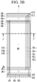
- FIG. 3B is an enlarged view of R region in FIG. 3A .
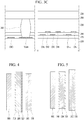
- FIG. 3C is a view taken along I-I' of FIG. 3A and II-II' of FIG. 3B .
- the barrier panel 200 of the stereoscopic display device may include a lower barrier substrate 210, an upper barrier substrate 220, a liquid-crystal layer 230, channel electrodes CH1-CHn, a barrier insulating layer 240, a common electrode 250, and link lines LB1-LBn, UB1-UBn, LT1, LT2, UT1 and UT2.
- the lower barrier substrate 210 and the upper barrier substrate 220 may include an insulating material.
- the lower barrier substrate 210 and the upper barrier substrate 220 may include a transparent material.
- the lower barrier substrate 210 and the upper barrier substrate 220 may include glass.
- the liquid crystal layer 230 may be disposed between the lower barrier substrate 210 and the upper barrier substrate 220.
- the liquid crystal layer 230 may include a liquid crystal rotated by an electric field which applied to the outside.
- the liquid crystal in the liquid crystal layer 230 may be TN type or ECB (electrically controlled birefringence) type.
- the channel electrodes CH1-CHn may be disposed between the lower barrier substrate 210 and the liquid crystal layer 230.
- the channel electrodes may be disposed at regular intervals.
- the channel electrodes may be insulated from each other by the barrier insulating layer 240.
- the channel electrodes CH1-CHn may be a multi-layer structure separated by the barrier insulating layer 240.
- the barrier insulating layer 240 may include an insulating material.
- the barrier insulating layer 240 may include silicon oxide or silicon nitride.
- the barrier panel 200 may selectively transmit or block light.
- the channel electrodes CH1-CHn may cross an active area AA in which transmitting regions and blocking regions are formed.
- the channel electrodes CH1-CHn may include a conductive material.
- the channel electrodes CH1-CHn may include a transparent material.
- the channel electrodes CH1-CHn may be formed of ITO or IZO.
- the common electrode 250 may be disposed between the liquid crystal layer 230 and the upper barrier substrate 220.
- the common electrode 250 may be formed on the upper barrier substrate 220.
- the common electrode 250 may form a vertical electric field with the channel electrodes CH1-CHn.
- the liquid crystal in the liquid crystal layer 230 may be rotated according to the vertical electric field formed between the channel electrodes CH1-CHn and the common electrode 250.
- the transmitting regions and the blocking regions may be formed by the rotation of the liquid crystal according to signal applied to the corresponding channel electrode CH1-CHn
- the common electrode 250 may include a conductive material.
- the common electrode 250 may include a transparent material.
- the common electrode 250 may be formed of ITO or IZO.
- the link lines LB1-LBn, UB1-UBn, LT1, LT2, UT1 and UT2 may be disposed on a peripheral area PA which is disposed outside the active area AA.
- the link lines LB1-LBn, UB1-UBn, LT1, LT2, UT1 and UT2 may be connected to the channel electrode CH1-CHn.
- Each of the channel electrodes CH1-Chn may be connected to the barrier driver 600 through one of the link lines LB1-LBn, UB1-UBn, LT1, LT2, UT1 and UT2.
- the link lines LB1-LBn, UB1-UBn, LT1, LT2, UT1 and UT2 may be connected to the channel electrodes CH1-CHn, individually.
- the link lines LB1-LBn, UB1-UBn, LT1, LT2, UT1 and UT2 may include first link lines LB1-LBn, and second link lines UB1-UBn.
- the first link lines LB1-LBn may be connected to an end portion of the channel electrodes CH1-CHn.
- the second link lines UB1-UBn may be connected to another end portion of the channel electrodes CH1-CHn which is not connected to the first link lines LB1-LBn.
- the end portion of the channel electrodes connected to the second link lines UB1-UBn may be opposite to the end portion of the channel electrodes connected to the first link lines LB1-LBn.
- the second link lines UB1-UBn may be extended along the active area AA.
- the second link lines UB1-UBn may include a region parallel with the channel electrodes CH1-CHn on a side of the active area AA.
- a length of the first link lines LB1-LBn connected to an end portion of each channel electrode CH1-CHn may be shorter than a length of the second link lines UB1-UBn connected to another end portion of the corresponding channel electrode CH1-CHn.
- a size of the peripheral area PA on which the link lines LB1-LBn, UB1-UBn, LT1, LT2, UT1 and UT2 are disposed may be minimized. Therefore, in the stereoscopic display device according to the embodiment of the present invention, the shift of the transmitting regions and the blocking regions by the channel electrodes CH1-Chn may be efficiently performed.
- the link lines LB1-LBn, UB1-UBn, LT1, LT2, UT1 and UT2 may intersect the channel electrodes CH1-CHn.
- the number of the link lines LB1-LBn, UB1-UBn, LT1, LT2, UT1 and UT2 in which each channel electrode CH1-CHn crosses, may be the same or constant.
- the number of the first link lines LB1-LBn and the second link lines UB1-UBn across a first channel electrode CH1 may be the same as the number of the first link lines LB1-LBn and the second link lines UB1-UBn across a second channel electrode CH2 which is disposed close to the first channel electrode CH1.
- the load deviation of the channels electrodes CH1-CHn may be prevented. Therefore, in the stereoscopic display device according to the embodiment of the present invention, the occurrence of the dim line or the dark line due to the load deviation may be prevented.
- the number of the first link lines LB1-LBn across the first channel electrode CH1 may be different from the number of the first link lines LB1-LBn across the second channel electrode CH2.
- the number of the second link lines UB1-UBn across the first channel electrode CH1 may be different from the number of the second link lines UB1-UBn across the second channel electrode CH2.
- the number of the first link lines LB1-LBn in which each channel electrode CH1-CHn crosses or being crossed by a channel electrode CH1-CHn may be in inverse proportion to the number of the second link lines UB1-UBn intersecting the corresponding channel electrode CH1-CHn, i.e.
- the link lines LB1-LBn, UB1-UBn, LT1, LT2, UT1 and UT2 may include a conductive material.
- the link lines LB1-LBn, UB1-UBn, LT1, LT2, UT1 and UT2 may a material having a relatively high conductivity.
- the link lines LB1-LBn, UB1-UBn, LT1, LT2, UT1 and UT2 may include a metal, such as aluminum (Al).
- the barrier panel 200 of the stereoscopic display device may further include trigger electrodes TC1 and TC2 which are disposed side by side between adjacent two channel electrodes in order to prevent the occurrence of a bright line or a dark line due to the shift of the transmitting regions and the blocking regions.
- the trigger electrodes TC1 and TC2 may be disposed between the channel electrodes CH1-CHn.
- the trigger electrodes TC1 and TC2 may cross the active area AA.
- the link lines LB1-LBn, UB1-UBn, LT1, LT2, UT1 and UT2 may further include trigger lines LT1, LT2, UT1 and UT2 connected to the trigger electrodes TC1 and TC2.
- the trigger lines LT1, LT2, UT1 and UT2 may include first trigger lines LT1 and LT2 connected to an end portion of the trigger electrodes TC1 and TC2, and second trigger lines UT1 and UT2 connected to another end portion of the trigger electrodes TC1 and TC2.
- the number of the link lines LB1-LBn, UB1-UBn, LT1, LT2, UT1 and UT2 intersecting each trigger electrode TC1 and TC2 may be different from the number of the link lines LB1-LBn, UB1-UBn, LT1, LT2, UT1 and UT2 intersecting each channel electrodes CH1-CHn.
- the trigger lines LT1, LT2, UT1 and UT2 may be disposed outside the link lines LB1-LBn and UB1-UBn connected to the channel electrodes CH1-CHn which form the transmitting regions and/or the blocking regions in a certain range of the active area AA.
- the number of the link lines LB1-LBn, UB1-UBn, LT1, LT2, UT1 and UT2 intersecting each trigger electrode TC1 and TC2 may be larger than the number of the link lines LB1-LBn, UB1-UBn, LT1, LT2, UT1 and UT2 intersecting each channel electrodes CH1-CHn.
- the stereoscopic display device according to the embodiment of the present invention may prevent an excessive load from being applied to the channel electrodes CH1-CHn by trigger lines LT1, LT2, UT1 and UT2.
- the number of the link lines LB1-LBn, UB1-UBn, LT1, LT2, UT1 and UT2 intersecting each trigger electrode TC1 and TC2 may be different from the number of the link lines LB1-LBn, UB1-UBn, LT1, LT2, UT1 and UT2 intersecting the trigger electrode TC1 and TC2 disposed adjacent the corresponding trigger electrode TC1 and TC2.
- the number of the link lines LB1-LBn, UB1-UBn, LT1, LT2, UT1 and UT2 intersecting first trigger electrode TC1 may be different from the number of the link lines LB1-LBn, UB1-UBn, LT1, LT2, UT1 and UT2 intersecting second trigger electrode TC2 which is disposed close to the first trigger electrode TC1.
- the barrier panel 200 of the stereoscopic display device may further include common voltage supply line Vcom and ground line GND which are disposed on the peripheral area PA.
- the common voltage supply line Vcom and the ground line GND may be disposed outside the link lines LB1-LBn, UB1-UBn, LT1, LT2, UT1 and UT2.
- the common voltage supply line Vcom may be disposed between the ground line GND and the link lines LB1-LBn, UB1-UBn, LT1, LT2, UT1 and UT2.
- the common voltage supply line Vcom and the ground line GND may include a material different from the channel electrodes CH1-CHn.
- the common voltage supply line Vcom and the ground line GND may include a metal.
- the common voltage supply line Vcom and the ground line GND may include a material same as the link lines LB1-LBn, UB1-UBn, LT1, LT2, UT1 and UT2.
- the barrier panel 200 of the stereoscopic display device may further include a barrier buffer layer 215 which covers the link lines LB1-LBn, UB1-UBn, LT1, LT2, UT1 and UT2, the common voltage supply line Vcom, and the ground line GND, and is extended between the lower substrate 210 and the channel electrodes CH1-CHn.
- the barrier buffer layer 215 may include an insulating material.
- the barrier buffer layer 215 may be silicon oxide.
- the common voltage supply line Vcom may be connected to the common electrode 250.
- a sealing member 260 for sealing the liquid crystal layer 230 may include a conductive material.
- the sealing member 260 may be in direct contact with the common electrode 250 and the common voltage supply line Vcom.
- the common electrode 250 may be connected to the common voltage supply line Vcom by the sealing member 260.
- the display driver 300 may drive the display panel 100.
- the display panel 100 may receive signals for realizing the image from the display driver 300.
- the display driver 300 may include a data driver 310 and a scan driver 320.
- the data driver 310 may provide a data signal to the display panel 100.
- the scan driver 320 may sequentially apply a scan signal to the display panel 100.
- the data signal provided by the data driver 310 may be synchronized with the scan signal applied from the scan driver 320.
- the timing controller 400 may provide a signal for the operation of the display driver 300.
- the timing controller 400 may provide digital video data and source timing control signal to the data driver 310.
- the scan driver 320 may receive clock signals, reset clock signals and start signals from the timing controller 400.
- the viewing location detecting part 500 may detect the location of the viewer.
- the viewing location detecting part 500 may detect the position information of the viewer viewing the image realized by the display panel 100 and the barrier panel 200.
- the viewing location detecting part 500 may include a camera.
- the barrier driver 600 may drive the barrier panel 200.
- the barrier driver 600 may apply a voltage the channel electrode CH1-CHn through the link lines LB1-LBn, UB1-UBn, LT1, LT2, UT1 and UT2, individually.
- the barrier driver 600 may control the channel electrodes CH1-CHn of the barrier panel 200 according to the location of the viewer.
- the barrier driver 600 may adjust the signal applied to the link lines LB1-LBn, UB1-UBn, LT1, LT2, UT1 and UT2 which are individually connected to channel electrodes CH1-CHn according to the signal of the viewing location detecting part 500.
- a size of the peripheral area PA of the barrier panel 200 may not increase greatly even when the number of the channel electrodes CH1-CHn is increased in order to smoothly moving a proper viewing range for the stereoscopic image according to the location of the viewer.
- the load deviation of the channel electrodes CH1-CHn may be prevented.
- the occurrence of the dim line or the dark line due to the load deviation may be prevented. Therefore, in the stereoscopic display device according to the embodiment of the present invention, the process efficiency and the quality of the stereoscopic image may be improved.
- the stereoscopic display device may include a structure for preventing the reflection of the external light.
- the stereoscopic display device may further include a quarter-wave plate 800 between the display panel 100 and a front linear polarizer 710, as shown in FIG. 2A .
- the quarter-wave plate 800 may be in direct contact with the display panel 100 and the front linear polarizer 710.
- a rear linear polarizer 720 may be disposed on an outer surface of the barrier panel 200.
- the stereoscopic display device is described that the barrier panel 200 is disposed on the display panel 100 including the light-emitting element 140.
- the barrier panel 200 may be disposed between the display panel 100 and the light-emitting element 900, as shown in FIG. 4 .
- the display panel 100 of the stereoscopic display device according to another embodiment of the present invention may be a liquid crystal panel.
- the light-emitting element 900 may function as a backlight unit.
- a front linear polarizer 710 and a rear linear polarizer 720 may be in direct contact with the barrier panel 200.
- An image linear polarizer 730 may be disposed on an outer surface of the display panel 100.
- the proper viewing range for the stereoscopic image may be smoothly moved according to the location of the viewer regardless of the relative position of the display panel 100 and the barrier panel 200.
- the stereoscopic display device is described that the barrier panel 200 is disposed between the light-emitting element 900 and the display panel 100.
- the display panel 100 may be disposed between the light-emitting element 900 and the barrier panel 200, as shown in FIG. 5 .
- An image linear polarizer 740 may be disposed between the light-emitting element 900 and the display panel 100.
- the image linear polarizer 740 and the front linear polarizer 710 may be in direct contact with the display panel 100.
- a rear linear polarizer 720 may be disposed on an outer surface of the barrier panel 200.
- the stereoscopic display device may smoothly provide the stereoscopic image to the moving viewer in the display panel 100 and the barrier panel 200 at various positions.
- the stereoscopic display device may prevent the load deviation of the channel electrodes by adjusting the number of the link lines across each channel electrode to be the same. Also, in the stereoscopic display device according to the embodiments of the present invention, only the second link lines connected to an end portion of the channel electrodes which is different from an end portion connected the first link lines, may be extended along the active area. Thus, in the stereoscopic display device according to the embodiments of the present invention, the size of the peripheral area of the barrier panel may be minimized with preventing the occurrence of the dim line due to the load deviation of the channel electrodes. Therefore, in the stereoscopic display device according to the embodiments of the present invention, the process efficiency and the quality of the stereoscopic image may be increased.
Landscapes
- Physics & Mathematics (AREA)
- Engineering & Computer Science (AREA)
- General Physics & Mathematics (AREA)
- Nonlinear Science (AREA)
- Optics & Photonics (AREA)
- Mathematical Physics (AREA)
- Crystallography & Structural Chemistry (AREA)
- Chemical & Material Sciences (AREA)
- Multimedia (AREA)
- Signal Processing (AREA)
- Theoretical Computer Science (AREA)
- Computer Hardware Design (AREA)
- Geometry (AREA)
- Microelectronics & Electronic Packaging (AREA)
- Electroluminescent Light Sources (AREA)
- Devices For Indicating Variable Information By Combining Individual Elements (AREA)
- Testing, Inspecting, Measuring Of Stereoscopic Televisions And Televisions (AREA)
- Polarising Elements (AREA)
- Liquid Crystal (AREA)
Abstract
Description
- This application claims the priority of Korean Patent Application No.
10-2017-0114734, filed on September 07, 2017 - The present invention relates to a stereoscopic display device realizing a stereoscopic image by using a barrier panel.
- Generally, a display device includes a display panel which realizes an image. For example, the display device may include a liquid crystal panel having a liquid crystal, and/or an OLED panel having an organic light-emitting element.
- The display device may realize a stereoscopic image using a position difference of viewer's eyes. For example, a stereoscopic display device may differently provide an image realized by the display panel to the left eye and the right eye of the viewer, using the binocular disparity.
- The stereoscopic display device may include an eyeglasses type using a shutter, and a non-glasses type using a barrier panel. The barrier panel may separate the image provided to the left eye and the right eye of the viewer using a path difference of light emitted from the display panel. For example, the barrier panel may form transmitting regions and blocking regions by adjusting voltage applied to channel electrodes which are disposed at regular intervals. The blocking regions may be disposed between the transmitting regions.
- The barrier panel may include link lines for supply signal to the channel electrodes. Each of the channel electrodes may form a closed loop with the corresponding link line in order to prevent luminance deviation due to voltage drop.
- The barrier panel may shift a proper viewing range for a stereoscopic image according to a location of the viewer. For example, the barrier panel may move the transmitting regions and the blocking regions according to the location of the viewer, by individually adjusting the voltage applied to each channel electrode.
- However, when the number of the channel electrodes in the barrier panel may be increased to smoothly move the proper viewing range according to the location of the viewer, the number of the link lines for applying the signal to the channel electrodes may be increased. Thus, in the stereoscopic display device, a size a peripheral area which is disposed outside of the active area may be increased, so that an entire size of the barrier panel may be increased. And, when the number of the channel electrodes and the number of the link lines may be increased, the connection between the channel electrodes and the link lines may be complicated, and a deviation may occur in a load of the channel electrodes due to the link lines. Therefore, in the stereoscopic display device, a dim line or a dark line due to the load deviation of the channel electrode may occur.
- Accordingly, the present invention is directed to a stereoscopic display device that substantially obviates one or more problems due to limitations and disadvantages of the related art.
- An object of the present invention is to provide a stereoscopic display device capable of minimizing a size of a peripheral area disposed outside an active area in which transmitting regions and blocking regions are formed by channel electrodes.
- Another object of the present invention is to provide a stereoscopic display device capable of preventing the occurrence of a dim line or a dark line due to load deviation of the channel electrodes.
- Additional advantages, objects, and features of the invention will be set forth in part in the description which follows and in part will become apparent to those having ordinary skill in the art upon examination of the following or may be learned from practice of the invention. The objectives and other advantages of the invention may be realized and attained by the structure particularly pointed out in the written description and claims hereof as well as the appended drawings.
- To achieve these objects and other advantages and in accordance with the purpose of the invention, as embodied and broadly described herein, there is provided a stereoscopic display device including a display driver which drives a display panel; a barrier panel which is disposed on the display panel, the barrier panel includes channel electrodes and link lines, the channel electrodes cross an active area, the link lines are disposed outside the active area, the link lines are connected to a barrier driver; and the barrier driver which controls the channel electrodes through the link lines. The number of the link lines in which each channel electrode crosses is the same.
- The link lines may be connected to the channel electrodes, individually.
- The link lines may include first link lines and second link lines.
- The first link lines may be connected to an end portion of the channel electrodes.
- The second link lines may be connected to another end portion of the channel electrodes.
- The number of the first link lines in which each channel crosses, is inverse proportional with the number of the second link lines intersecting the corresponding channel electrode.
- The second link lines may include a region parallel with the channel electrodes on a side of the active region.
- The barrier panel may further include trigger electrodes between the channel electrodes.
- Preferably, the number of link lines in which each trigger electrode intersects may be different from the number of link lines in which each channel electrode intersects.
- The number of link lines in which each trigger electrode intersects may be larger than the number of link lines in which each channel electrode intersects.
- Preferably, the trigger electrode may be disposed parallel to the channel electrodes.
- Preferably, the trigger electrode may include a first trigger electrode and a second trigger electrode.
- Preferably, the first trigger electrode and a second trigger electrode may be disposed side by side between the adjacent two channel electrodes.
- The number of the link lines in which the second trigger electrode intersects may be different from the number of the first trigger electrode intersects.
- A location of the viewer may be detected by a viewing location detecting part.
- Preferably a barrier driver may provided to adjust the signal applied to the channel electrodes through the link lines according to the signal of the viewing location detecting part.
- The display panel may include a lower display substrate, a lower emission electrode, a light-emitting layer, an upper emission electrode and an upper display substrate, which are sequentially stacked.
- The accompanying drawings, which are included to provide a further understanding of the invention and are incorporated in and constitute a part of this application, illustrate embodiment(s) of the invention and together with the description serve to explain the principle of the invention. In the drawings:
-
FIG. 1 is a view schematically showing a stereoscopic display device according to an embodiment of the present invention; -
FIG. 2A is a view showing a display panel and a barrier panel of the stereoscopic display device according to the embodiment of the present invention; -
FIG. 2B is an enlarged view of P region inFIG. 2A ; -
FIG. 3A is a view schematically showing a wiring lines on the barrier panel of the stereoscopic display device according to the embodiment of the present invention; -
FIG. 3B is an enlarged view of R region inFIG. 3A ; -
FIG. 3C is a view taken along I-I' ofFIG. 3A and II-II' ofFIG. 3B ; and -
FIGS. 4 and 5 are views respectively showing the display device according to another embodiment of the present invention. - Hereinafter, details related to the above objects, technical configurations, and operational effects of the embodiments of the present invention will be clearly understood by the following detailed description with reference to the drawings, which illustrate some embodiments of the present invention. Here, the embodiments of the present invention are provided in order to allow the technical sprit of the present invention to be satisfactorily transferred to those skilled in the art, and thus the present invention may be embodied in other forms and is not limited to the embodiments described below.
- In addition, the same or extremely similar elements may be designated by the same reference numerals throughout the specification, and in the drawings, the lengths and thickness of layers and regions may be exaggerated for convenience. It will be understood that, when a first element is referred to as being "on" a second element, although the first element may be disposed on the second element so as to come into contact with the second element, a third element may be interposed between the first element and the second element.
- Here, terms such as, for example, "first" and "second" may be used to distinguish any one element with another element. However, the first element and the second element may be arbitrary named according to the convenience of those skilled in the art without departing the technical sprit of the present invention.
- The terms used in the specification of the present invention are merely used in order to describe particular embodiments, and are not intended to limit the scope of the present invention. For example, an element described in the singular form is intended to include a plurality of elements unless the context clearly indicates otherwise. In addition, in the specification of the present invention, it will be further understood that the terms "comprises" and "includes" specify the presence of stated features, integers, steps, operations, elements, components, and/or combinations thereof, but do not preclude the presence or addition of one or more other features, integers, steps, operations, elements, components, and/or combinations thereof.
- Unless otherwise defined, all terms (including technical and scientific terms) used herein have the same meaning as commonly understood by one of ordinary skill in the art to which example embodiments belong. It will be further understood that terms, such as those defined in commonly used dictionaries, should be interpreted as having a meaning that is consistent with their meaning in the context of the relevant art and should not be interpreted in an idealized or overly formal sense unless expressly so defined herein.
-
FIG. 1 is a view schematically showing a stereoscopic display device according to an embodiment of the present invention.FIG. 2A is a view showing a display panel and a barrier panel of the stereoscopic display device according to the embodiment of the present invention.FIG. 2B is an enlarged view of P region inFIG. 2A . - Referring
FIGS. 1, 2A and2B , the stereoscopic display device according to the embodiment of the present invention may include adisplay panel 100, abarrier panel 200, adisplay driver 300, atiming controller 400, a viewerlocation detecting part 500 and abarrier driver 600. - The
display panel 100 may realize an image which is provided to a viewer. For example, thedisplay panel 100 may include alower display substrate 110, a light-emittingelement 140 and anupper display substrate 180, which are sequentially stacked. The light-emittingelement 140 may generate light displaying a specific color to realize the image. For example, the light-emittingelement 140 may include alower emission element 141, a light-emittinglayer 142 and anupper emission element 143, which are sequentially stacked. The light-emittinglayer 142 may include an organic emission material or an inorganic emission material. For example, thedisplay panel 100 of the stereoscopic display device according to the embodiment of the present invention may be an OLED panel including an organic light-emitting element. - The
display panel 100 may further include athin film transistor 120 between thelower display substrate 110 and the light-emittingelement 140, anover-coat layer 130 covering thethin film transistor 120, and abank insulating layer 150 covering an edge of thelower emission electrode 141. Theover-coat layer 130 may remove a thickness difference due to thethin film transistor 120. The light-emittingelement 140 may be disposed on theover-coat layer 130. For example, theover-coat layer 130 may include a contact hole exposing drain electrode of thethin film transistor 120. - The
display panel 100 may further include anupper passivation layer 160 and anadhesive layer 170 which are disposed between the light-emittingelement 140 and theupper display substrate 180. Theupper passivation layer 160 may prevent damage of the light-emittingelement 140 due to the external impact and moisture. Theadhesive layer 170 may be disposed between theupper passivation layer 160 and theupper display substrate 180. Theupper display substrate 180 may be coupled to thelower display substrate 110 in which theupper passivation layer 160 is formed, by theadhesive layer 170. Theadhesive layer 170 may have a multi-layer structure. For example, theadhesive layer 170 may include a loweradhesive layer 171 and an upperadhesive layer 172. The upperadhesive layer 172 may be disposed between the loweradhesive layer 171 and theupper display substrate 180. The upperadhesive layer 172 may include a moisture-absorbingmaterial 170p. The loweradhesive layer 171 may relieve the stress applied to the light-emittingelement 140 due to the expansion of the moisture-absorbingmaterial 170p. - The
barrier panel 200 may be disposed on thedisplay panel 100. Thebarrier panel 200 may separate the image realized by thedisplay panel 100 to provide the left eye and the right eye of the viewer. For example, the image realized by thedisplay panel 100 may be stereoscopically recognized to the viewer by thebarrier panel 200. -
FIG. 3A is a view schematically showing a wiring lines on thebarrier panel 200 of the stereoscopic display device according to the embodiment of the present invention.FIG. 3B is an enlarged view of R region inFIG. 3A .FIG. 3C is a view taken along I-I' ofFIG. 3A and II-II' ofFIG. 3B . - Referring
FIGS. 1, 2A and3A to 3C , thebarrier panel 200 of the stereoscopic display device according to the embodiment of the present invention may include alower barrier substrate 210, anupper barrier substrate 220, a liquid-crystal layer 230, channel electrodes CH1-CHn, abarrier insulating layer 240, acommon electrode 250, and link lines LB1-LBn, UB1-UBn, LT1, LT2, UT1 and UT2. - The
lower barrier substrate 210 and theupper barrier substrate 220 may include an insulating material. Thelower barrier substrate 210 and theupper barrier substrate 220 may include a transparent material. For example, thelower barrier substrate 210 and theupper barrier substrate 220 may include glass. - The
liquid crystal layer 230 may be disposed between thelower barrier substrate 210 and theupper barrier substrate 220. Theliquid crystal layer 230 may include a liquid crystal rotated by an electric field which applied to the outside. For example, the liquid crystal in theliquid crystal layer 230 may be TN type or ECB (electrically controlled birefringence) type. - The channel electrodes CH1-CHn may be disposed between the
lower barrier substrate 210 and theliquid crystal layer 230. The channel electrodes may be disposed at regular intervals. The channel electrodes may be insulated from each other by thebarrier insulating layer 240. For example, the channel electrodes CH1-CHn may be a multi-layer structure separated by thebarrier insulating layer 240. Thebarrier insulating layer 240 may include an insulating material. For example, thebarrier insulating layer 240 may include silicon oxide or silicon nitride. - The
barrier panel 200 may selectively transmit or block light. For example, the channel electrodes CH1-CHn may cross an active area AA in which transmitting regions and blocking regions are formed. The channel electrodes CH1-CHn may include a conductive material. The channel electrodes CH1-CHn may include a transparent material. For example, the channel electrodes CH1-CHn may be formed of ITO or IZO. - The
common electrode 250 may be disposed between theliquid crystal layer 230 and theupper barrier substrate 220. For example, thecommon electrode 250 may be formed on theupper barrier substrate 220. Thecommon electrode 250 may form a vertical electric field with the channel electrodes CH1-CHn. The liquid crystal in theliquid crystal layer 230 may be rotated according to the vertical electric field formed between the channel electrodes CH1-CHn and thecommon electrode 250. The transmitting regions and the blocking regions may be formed by the rotation of the liquid crystal according to signal applied to the corresponding channel electrode CH1-CHn - The
common electrode 250 may include a conductive material. Thecommon electrode 250 may include a transparent material. For example, thecommon electrode 250 may be formed of ITO or IZO. - The link lines LB1-LBn, UB1-UBn, LT1, LT2, UT1 and UT2 may be disposed on a peripheral area PA which is disposed outside the active area AA. The link lines LB1-LBn, UB1-UBn, LT1, LT2, UT1 and UT2 may be connected to the channel electrode CH1-CHn. Each of the channel electrodes CH1-Chn may be connected to the
barrier driver 600 through one of the link lines LB1-LBn, UB1-UBn, LT1, LT2, UT1 and UT2. For example, the link lines LB1-LBn, UB1-UBn, LT1, LT2, UT1 and UT2 may be connected to the channel electrodes CH1-CHn, individually. - The link lines LB1-LBn, UB1-UBn, LT1, LT2, UT1 and UT2 may include first link lines LB1-LBn, and second link lines UB1-UBn. The first link lines LB1-LBn may be connected to an end portion of the channel electrodes CH1-CHn. The second link lines UB1-UBn may be connected to another end portion of the channel electrodes CH1-CHn which is not connected to the first link lines LB1-LBn. For example, the end portion of the channel electrodes connected to the second link lines UB1-UBn may be opposite to the end portion of the channel electrodes connected to the first link lines LB1-LBn. The second link lines UB1-UBn may be extended along the active area AA. For example, the second link lines UB1-UBn may include a region parallel with the channel electrodes CH1-CHn on a side of the active area AA. A length of the first link lines LB1-LBn connected to an end portion of each channel electrode CH1-CHn may be shorter than a length of the second link lines UB1-UBn connected to another end portion of the corresponding channel electrode CH1-CHn. Thus, in the stereoscopic display device according to the embodiment of the present invention, a size of the peripheral area PA on which the link lines LB1-LBn, UB1-UBn, LT1, LT2, UT1 and UT2 are disposed, may be minimized. Therefore, in the stereoscopic display device according to the embodiment of the present invention, the shift of the transmitting regions and the blocking regions by the channel electrodes CH1-Chn may be efficiently performed.
- The link lines LB1-LBn, UB1-UBn, LT1, LT2, UT1 and UT2 may intersect the channel electrodes CH1-CHn. The number of the link lines LB1-LBn, UB1-UBn, LT1, LT2, UT1 and UT2 in which each channel electrode CH1-CHn crosses, may be the same or constant. For example, the number of the first link lines LB1-LBn and the second link lines UB1-UBn across a first channel electrode CH1 may be the same as the number of the first link lines LB1-LBn and the second link lines UB1-UBn across a second channel electrode CH2 which is disposed close to the first channel electrode CH1. Thus, in the stereoscopic display device according to the embodiment of the present invention, the load deviation of the channels electrodes CH1-CHn may be prevented. Therefore, in the stereoscopic display device according to the embodiment of the present invention, the occurrence of the dim line or the dark line due to the load deviation may be prevented.
- The number of the first link lines LB1-LBn across the first channel electrode CH1 may be different from the number of the first link lines LB1-LBn across the second channel electrode CH2. The number of the second link lines UB1-UBn across the first channel electrode CH1 may be different from the number of the second link lines UB1-UBn across the second channel electrode CH2. For example, the number of the first link lines LB1-LBn in which each channel electrode CH1-CHn crosses or being crossed by a channel electrode CH1-CHn may be in inverse proportion to the number of the second link lines UB1-UBn intersecting the corresponding channel electrode CH1-CHn, i.e. if there are 18 link lines and a channel electrode (CHI) is crossed by 9 link lines in total then it is crossing 7 first link lines and two second link lines For the channel electrode CH2 in
Fig. 3B there are also 9 link lines in total being crossed by channel electrode CH2, there are 6 first link lines and 3 second link lines being crossed by the channel electrode CH2. - The link lines LB1-LBn, UB1-UBn, LT1, LT2, UT1 and UT2 may include a conductive material. The link lines LB1-LBn, UB1-UBn, LT1, LT2, UT1 and UT2 may a material having a relatively high conductivity. For example, the link lines LB1-LBn, UB1-UBn, LT1, LT2, UT1 and UT2 may include a metal, such as aluminum (Al).
- The
barrier panel 200 of the stereoscopic display device according to the embodiment of the present invention may further include trigger electrodes TC1 and TC2 which are disposed side by side between adjacent two channel electrodes in order to prevent the occurrence of a bright line or a dark line due to the shift of the transmitting regions and the blocking regions. The trigger electrodes TC1 and TC2 may be disposed between the channel electrodes CH1-CHn. For example, the trigger electrodes TC1 and TC2 may cross the active area AA. - The link lines LB1-LBn, UB1-UBn, LT1, LT2, UT1 and UT2 may further include trigger lines LT1, LT2, UT1 and UT2 connected to the trigger electrodes TC1 and TC2. The trigger lines LT1, LT2, UT1 and UT2 may include first trigger lines LT1 and LT2 connected to an end portion of the trigger electrodes TC1 and TC2, and second trigger lines UT1 and UT2 connected to another end portion of the trigger electrodes TC1 and TC2.
- The number of the link lines LB1-LBn, UB1-UBn, LT1, LT2, UT1 and UT2 intersecting each trigger electrode TC1 and TC2 may be different from the number of the link lines LB1-LBn, UB1-UBn, LT1, LT2, UT1 and UT2 intersecting each channel electrodes CH1-CHn. For example, the trigger lines LT1, LT2, UT1 and UT2 may be disposed outside the link lines LB1-LBn and UB1-UBn connected to the channel electrodes CH1-CHn which form the transmitting regions and/or the blocking regions in a certain range of the active area AA. The number of the link lines LB1-LBn, UB1-UBn, LT1, LT2, UT1 and UT2 intersecting each trigger electrode TC1 and TC2 may be larger than the number of the link lines LB1-LBn, UB1-UBn, LT1, LT2, UT1 and UT2 intersecting each channel electrodes CH1-CHn. Thus, the stereoscopic display device according to the embodiment of the present invention may prevent an excessive load from being applied to the channel electrodes CH1-CHn by trigger lines LT1, LT2, UT1 and UT2. The number of the link lines LB1-LBn, UB1-UBn, LT1, LT2, UT1 and UT2 intersecting each trigger electrode TC1 and TC2 may be different from the number of the link lines LB1-LBn, UB1-UBn, LT1, LT2, UT1 and UT2 intersecting the trigger electrode TC1 and TC2 disposed adjacent the corresponding trigger electrode TC1 and TC2. For example, the number of the link lines LB1-LBn, UB1-UBn, LT1, LT2, UT1 and UT2 intersecting first trigger electrode TC1 may be different from the number of the link lines LB1-LBn, UB1-UBn, LT1, LT2, UT1 and UT2 intersecting second trigger electrode TC2 which is disposed close to the first trigger electrode TC1.
- The
barrier panel 200 of the stereoscopic display device according to the embodiment of the present invention may further include common voltage supply line Vcom and ground line GND which are disposed on the peripheral area PA. The common voltage supply line Vcom and the ground line GND may be disposed outside the link lines LB1-LBn, UB1-UBn, LT1, LT2, UT1 and UT2. For example, the common voltage supply line Vcom may be disposed between the ground line GND and the link lines LB1-LBn, UB1-UBn, LT1, LT2, UT1 and UT2. - The common voltage supply line Vcom and the ground line GND may include a material different from the channel electrodes CH1-CHn. For example, the common voltage supply line Vcom and the ground line GND may include a metal. The common voltage supply line Vcom and the ground line GND may include a material same as the link lines LB1-LBn, UB1-UBn, LT1, LT2, UT1 and UT2.
- The
barrier panel 200 of the stereoscopic display device according to the embodiment of the present invention may further include abarrier buffer layer 215 which covers the link lines LB1-LBn, UB1-UBn, LT1, LT2, UT1 and UT2, the common voltage supply line Vcom, and the ground line GND, and is extended between thelower substrate 210 and the channel electrodes CH1-CHn. Thebarrier buffer layer 215 may include an insulating material. For example, thebarrier buffer layer 215 may be silicon oxide. - The common voltage supply line Vcom may be connected to the
common electrode 250. For example, in thebarrier panel 200 of the stereoscopic display device according to the embodiment of the present invention, a sealingmember 260 for sealing theliquid crystal layer 230 may include a conductive material. The sealingmember 260 may be in direct contact with thecommon electrode 250 and the common voltage supply line Vcom. Thecommon electrode 250 may be connected to the common voltage supply line Vcom by the sealingmember 260. - The
display driver 300 may drive thedisplay panel 100. Thedisplay panel 100 may receive signals for realizing the image from thedisplay driver 300. For example, thedisplay driver 300 may include adata driver 310 and ascan driver 320. - The
data driver 310 may provide a data signal to thedisplay panel 100. Thescan driver 320 may sequentially apply a scan signal to thedisplay panel 100. The data signal provided by thedata driver 310 may be synchronized with the scan signal applied from thescan driver 320. - The
timing controller 400 may provide a signal for the operation of thedisplay driver 300. For example, thetiming controller 400 may provide digital video data and source timing control signal to thedata driver 310. Thescan driver 320 may receive clock signals, reset clock signals and start signals from thetiming controller 400. - The viewing
location detecting part 500 may detect the location of the viewer. For example, the viewinglocation detecting part 500 may detect the position information of the viewer viewing the image realized by thedisplay panel 100 and thebarrier panel 200. The viewinglocation detecting part 500 may include a camera. - The
barrier driver 600 may drive thebarrier panel 200. For example, thebarrier driver 600 may apply a voltage the channel electrode CH1-CHn through the link lines LB1-LBn, UB1-UBn, LT1, LT2, UT1 and UT2, individually. Thebarrier driver 600 may control the channel electrodes CH1-CHn of thebarrier panel 200 according to the location of the viewer. For example, thebarrier driver 600 may adjust the signal applied to the link lines LB1-LBn, UB1-UBn, LT1, LT2, UT1 and UT2 which are individually connected to channel electrodes CH1-CHn according to the signal of the viewinglocation detecting part 500. - Accordingly, in the stereoscopic display device according to the embodiment of the present invention, a size of the peripheral area PA of the
barrier panel 200 may not increase greatly even when the number of the channel electrodes CH1-CHn is increased in order to smoothly moving a proper viewing range for the stereoscopic image according to the location of the viewer. And, in the stereoscopic display device according to the embodiment of the present invention, the load deviation of the channel electrodes CH1-CHn may be prevented. Thus, in the stereoscopic display device according to the embodiment of the present invention, the occurrence of the dim line or the dark line due to the load deviation may be prevented. Therefore, in the stereoscopic display device according to the embodiment of the present invention, the process efficiency and the quality of the stereoscopic image may be improved. - The stereoscopic display device according to the embodiment of the present invention may include a structure for preventing the reflection of the external light. For example, the stereoscopic display device according to the embodiment of the present invention may further include a quarter-
wave plate 800 between thedisplay panel 100 and a frontlinear polarizer 710, as shown inFIG. 2A . The quarter-wave plate 800 may be in direct contact with thedisplay panel 100 and the frontlinear polarizer 710. A rearlinear polarizer 720 may be disposed on an outer surface of thebarrier panel 200. - The stereoscopic display device according to the embodiment of the present invention is described that the
barrier panel 200 is disposed on thedisplay panel 100 including the light-emittingelement 140. However, in the stereoscopic display device according to another embodiment of the present invention, thebarrier panel 200 may be disposed between thedisplay panel 100 and the light-emittingelement 900, as shown inFIG. 4 . For example, thedisplay panel 100 of the stereoscopic display device according to another embodiment of the present invention may be a liquid crystal panel. The light-emittingelement 900 may function as a backlight unit. A frontlinear polarizer 710 and a rearlinear polarizer 720 may be in direct contact with thebarrier panel 200. An imagelinear polarizer 730 may be disposed on an outer surface of thedisplay panel 100. Thus, in the stereoscopic display device according to another embodiment of the present invention, the proper viewing range for the stereoscopic image may be smoothly moved according to the location of the viewer regardless of the relative position of thedisplay panel 100 and thebarrier panel 200. - The stereoscopic display device according to another embodiment of the present invention is described that the
barrier panel 200 is disposed between the light-emittingelement 900 and thedisplay panel 100. However, in the stereoscopic display device according to further another embodiment of the present invention, thedisplay panel 100 may be disposed between the light-emittingelement 900 and thebarrier panel 200, as shown inFIG. 5 . An imagelinear polarizer 740 may be disposed between the light-emittingelement 900 and thedisplay panel 100. The imagelinear polarizer 740 and the frontlinear polarizer 710 may be in direct contact with thedisplay panel 100. A rearlinear polarizer 720 may be disposed on an outer surface of thebarrier panel 200. Thus, the stereoscopic display device according to further another embodiment of the present invention may smoothly provide the stereoscopic image to the moving viewer in thedisplay panel 100 and thebarrier panel 200 at various positions. - In the result, the stereoscopic display device according to the embodiments of the present invention may prevent the load deviation of the channel electrodes by adjusting the number of the link lines across each channel electrode to be the same. Also, in the stereoscopic display device according to the embodiments of the present invention, only the second link lines connected to an end portion of the channel electrodes which is different from an end portion connected the first link lines, may be extended along the active area. Thus, in the stereoscopic display device according to the embodiments of the present invention, the size of the peripheral area of the barrier panel may be minimized with preventing the occurrence of the dim line due to the load deviation of the channel electrodes. Therefore, in the stereoscopic display device according to the embodiments of the present invention, the process efficiency and the quality of the stereoscopic image may be increased.
Claims (15)
- A stereoscopic display device comprising:a display panel (100);a display driver (300) driving the display panel (100);a barrier panel (200) on the display panel (100), the barrier panel (200) including channel electrodes (CH1-CHn) across an active area (AA), and link lines (LB1-LBn, UB1-UBn, LT1, LT2, UT1, UT2) disposed outside the active area (AA); anda barrier driver (600) controlling the channel electrodes (CH1-CHn) through the link lines (LB1-LBn, UB1-UBn, LT1, LT2, UT1, UT2),wherein the number of the link lines (LB1-LBn, UB1-UBn, LT1, LT2, UT1, UT2) being crossed by a channel electrode (CH1-CHn), is constant.
- The stereoscopic display device according to claim 1, wherein each channel electrode (CH1-CHn) is connected to two link lines (LB1-LBn, UB1-UBn, LT1, LT2, UT1, UT2).
- The stereoscopic display device according to claim 1 or 2, wherein the link lines (LB1-LBn, UB1-UBn, LT1, LT2, UT1, UT2) include first link lines (LB1-LBn) connected to an end portion of the channel electrodes (CH1-CHn), and second link lines (UB1-UBn) connected to another end portion of the channel electrodes (CH1-CHn).
- The stereoscopic display device according to any one of claims 1-3, wherein the number of the first link lines (LB1-LBn) being crossed by each channel electrode (CH1-CHn), is in inverse proportion to the number of the second link lines (UB1-UBn) intersecting the corresponding channel electrode (CH1-CHn).
- The stereoscopic display device according to claim 3 or 4, wherein the second link lines (UB1-UBn) include a region parallel with the channel electrodes (CH1-CHn) on a side of the active area (AA).
- The stereoscopic display device according to any one of the preceding claims, wherein the barrier panel (200) further includes trigger electrodes (TC1, TC2) between the channel electrodes (CH1-CHn).
- The stereoscopic display device according to claim 6, wherein the number of the link lines LB1-LBn, UB1-UBn, LT1, LT2, UT1, UT2) crossing a trigger electrode (TC1, TC2), is different from the number of the link lines LB1-LBn, UB1-UBn, LT1, LT2, UT1, UT2) intersecting a channel electrode (CH1-CHn),
preferably, the number of the link lines intersecting each trigger electrode (TC1, TC2) is larger than the number of the link lines intersecting each channel electrode (CH1-CHn). - The stereoscopic display device according to claim 6 or 7, wherein the trigger electrodes (TC1, TC2) includes a first trigger electrode (TC1) and a second trigger electrode (TC2) which are disposed side by side between adjacent two channel electrodes (CH1-CHn), and
wherein the number of the link lines intersecting the second trigger electrode (TC2) is different from the number of the link lines intersecting the first trigger electrodes (TC1). - The stereoscopic display device according to any one of the preceding claims, further comprising a viewing location detecting part (500) detecting a location of a viewer.
- The stereoscopic display device according to claim 9, wherein the barrier driver (600) is configured to control a signal applied to the channel electrodes (CH1-CHn) through the link lines according to the signal of the viewing location detecting part (500).
- The stereoscopic display device according to any one of the preceding claims, wherein the display panel (100) includes a lower display substrate (110), a lower emission electrode (141), a light-emitting layer (142), an upper emission electrode (143) and an upper display substrate (180), which are sequentially stacked.
- The stereoscopic display device according to any one of the claims 3 -11, wherein only the second link lines (UB1-UBn) are extended along the active area (AA).
- The stereoscopic display device according to any one of the preceding claims, further comprising a front linear polarizer (710), a rear linear polarizer (720) and a quarter-wave plate (800), wherein the quarter-wave plate (800) is in direct contact with the display panel (100) and the front linear polarizer (710), wherein the rear linear polarizer (720) is disposed on an outer surface of the barrier panel (200).
- The stereoscopic display device according to any one of the preceding claims, further comprising a front linear polarizer (710), a rear linear polarizer (720) and an image linear polarizer (730), wherein the front linear polarizer (710) and the rear linear polarizer (720) are in direct contact with the barrier panel (200), the image linear polarizer (730) is disposed on an outer surface of the display panel (100).
- The stereoscopic display device according to any one of the preceding claims, further comprising a front linear polarizer (710), a rear linear polarizer (720) and an image linear polarizer (740), wherein the image linear polarizer (740) and the front linear polarizer (710) are in direct contact with the display panel (100), the rear linear polarizer (720) is disposed on an outer surface of the barrier panel (200).
Applications Claiming Priority (1)
| Application Number | Priority Date | Filing Date | Title |
|---|---|---|---|
| KR1020170114734A KR102056677B1 (en) | 2017-09-07 | 2017-09-07 | Stereoscopic Display device having a barrier panel |
Publications (1)
| Publication Number | Publication Date |
|---|---|
| EP3454321A1 true EP3454321A1 (en) | 2019-03-13 |
Family
ID=63528529
Family Applications (1)
| Application Number | Title | Priority Date | Filing Date |
|---|---|---|---|
| EP18192866.4A Pending EP3454321A1 (en) | 2017-09-07 | 2018-09-06 | Stereoscopic display device having a barrier panel |
Country Status (5)
| Country | Link |
|---|---|
| US (2) | US10747018B2 (en) |
| EP (1) | EP3454321A1 (en) |
| JP (1) | JP6751121B2 (en) |
| KR (1) | KR102056677B1 (en) |
| CN (1) | CN109473054B (en) |
Families Citing this family (2)
| Publication number | Priority date | Publication date | Assignee | Title |
|---|---|---|---|---|
| JP2022157685A (en) * | 2021-03-31 | 2022-10-14 | 株式会社ジャパンディスプレイ | Liquid crystal display device and display device |
| KR20230028671A (en) * | 2021-08-20 | 2023-03-02 | 삼성디스플레이 주식회사 | Stereoscopic image display device |
Citations (3)
| Publication number | Priority date | Publication date | Assignee | Title |
|---|---|---|---|---|
| US20090153653A1 (en) * | 2007-12-14 | 2009-06-18 | Byung Joo Lee | Electrically-Driven Liquid Crystal Lens and stereoscopic Display Device Using the Same |
| US20160004128A1 (en) * | 2014-01-17 | 2016-01-07 | Boe Technology Group Co., Ltd. | Liquid crystal lens and three-dimensional display device |
| US20160037155A1 (en) * | 2013-03-11 | 2016-02-04 | Sharp Kabushiki Kaisha | Stereoscopic display device |
Family Cites Families (29)
| Publication number | Priority date | Publication date | Assignee | Title |
|---|---|---|---|---|
| JP2005070353A (en) | 2003-08-22 | 2005-03-17 | Sharp Corp | Image display device |
| JP4053508B2 (en) * | 2004-03-10 | 2008-02-27 | シャープ株式会社 | Display device driving method and display device |
| KR101087568B1 (en) * | 2004-12-30 | 2011-11-28 | 엘지디스플레이 주식회사 | Parallax barrier liquid crystal panel for stereoscopic image display device and manufacturing method |
| KR100720944B1 (en) | 2005-08-23 | 2007-05-23 | 한국전자통신연구원 | Transmitter and Pilot Channel Configuration in Frequency Division Multiple Access Communication System |
| KR20070023849A (en) * | 2005-08-25 | 2007-03-02 | (주)엔디스 | Wide viewing angle stereoscopic display |
| KR20080003226A (en) * | 2006-06-30 | 2008-01-07 | 엘지.필립스 엘시디 주식회사 | LCD display device |
| KR101593546B1 (en) * | 2008-11-01 | 2016-02-17 | 엘지디스플레이 주식회사 | Liquid crystal lens and driving method thereof |
| JP2011209346A (en) | 2010-03-29 | 2011-10-20 | Casio Computer Co Ltd | Display device, drive control method of the same, and electronic device |
| KR101781549B1 (en) * | 2010-12-02 | 2017-09-27 | 삼성디스플레이 주식회사 | Display substrate and method of manufacturing the same |
| JP5798619B2 (en) * | 2011-04-22 | 2015-10-21 | シャープ株式会社 | Display device |
| CN102799010B (en) * | 2011-05-23 | 2015-06-10 | 余瑞兰 | Liquid crystal display for displaying stereoscopic images |
| KR101831652B1 (en) * | 2011-09-07 | 2018-02-26 | 엘지디스플레이 주식회사 | Stereoscopic image display device and driving method thereof |
| CN103163650A (en) | 2011-12-08 | 2013-06-19 | 武汉天马微电子有限公司 | Glasses-free 3D grating structure |
| EP2633828B1 (en) * | 2012-02-28 | 2019-08-07 | Cook Medical Technologies LLC | Introducer assembly |
| KR20130101236A (en) | 2012-03-05 | 2013-09-13 | 삼성디스플레이 주식회사 | Barrier substrate, barrier panel having the same and display apparatus having the same |
| KR20140073133A (en) * | 2012-12-06 | 2014-06-16 | 삼성디스플레이 주식회사 | Display apparatus |
| KR20140102449A (en) * | 2013-02-14 | 2014-08-22 | 한국전자통신연구원 | Display panel, 3d display apparatus and display method based on segmented parallax barrier |
| KR102527503B1 (en) * | 2013-02-27 | 2023-04-28 | 시리얼 테크놀로지즈 에스.에이. | Optical liquid-crystal phase modulator |
| KR20150016459A (en) | 2013-08-02 | 2015-02-12 | 삼성디스플레이 주식회사 | Display device and method for manufacturing thereof |
| KR102142250B1 (en) | 2013-08-30 | 2020-08-07 | 엘지디스플레이 주식회사 | 3-dimension image display device and driving method thereof |
| WO2015059996A1 (en) | 2013-10-24 | 2015-04-30 | シャープ株式会社 | Three-dimensional display device |
| US9874770B2 (en) * | 2013-11-15 | 2018-01-23 | Sharp Kabushiki Kaisha | Display device |
| US20170045763A1 (en) * | 2014-04-22 | 2017-02-16 | Sharp Kabushiki Kaisha | Stereoscopic display device |
| KR102199610B1 (en) | 2014-09-03 | 2021-01-08 | 엘지디스플레이 주식회사 | Image display apparatus |
| JP6573467B2 (en) * | 2015-03-31 | 2019-09-11 | 株式会社ジャパンディスプレイ | Image display device and liquid crystal panel |
| JP6514938B2 (en) | 2015-03-31 | 2019-05-15 | 株式会社ジャパンディスプレイ | Image display device and liquid crystal panel |
| CN106353916A (en) * | 2016-11-22 | 2017-01-25 | 北京小米移动软件有限公司 | Display device and display method |
| KR101888449B1 (en) * | 2017-04-18 | 2018-08-16 | 엘지디스플레이 주식회사 | Stereoscopic Display device having a barrier panel |
| KR101960391B1 (en) * | 2017-09-08 | 2019-03-20 | 엘지디스플레이 주식회사 | Stereoscopic Display device having a barrier panel |
-
2017
- 2017-09-07 KR KR1020170114734A patent/KR102056677B1/en active Active
-
2018
- 2018-09-06 US US16/123,502 patent/US10747018B2/en active Active
- 2018-09-06 CN CN201811038952.7A patent/CN109473054B/en active Active
- 2018-09-06 EP EP18192866.4A patent/EP3454321A1/en active Pending
- 2018-09-07 JP JP2018167765A patent/JP6751121B2/en active Active
-
2020
- 2020-07-08 US US16/923,928 patent/US10816819B1/en active Active
Patent Citations (3)
| Publication number | Priority date | Publication date | Assignee | Title |
|---|---|---|---|---|
| US20090153653A1 (en) * | 2007-12-14 | 2009-06-18 | Byung Joo Lee | Electrically-Driven Liquid Crystal Lens and stereoscopic Display Device Using the Same |
| US20160037155A1 (en) * | 2013-03-11 | 2016-02-04 | Sharp Kabushiki Kaisha | Stereoscopic display device |
| US20160004128A1 (en) * | 2014-01-17 | 2016-01-07 | Boe Technology Group Co., Ltd. | Liquid crystal lens and three-dimensional display device |
Also Published As
| Publication number | Publication date |
|---|---|
| KR20190027665A (en) | 2019-03-15 |
| US20200333627A1 (en) | 2020-10-22 |
| JP2019070792A (en) | 2019-05-09 |
| US10816819B1 (en) | 2020-10-27 |
| JP6751121B2 (en) | 2020-09-02 |
| CN109473054A (en) | 2019-03-15 |
| US10747018B2 (en) | 2020-08-18 |
| KR102056677B1 (en) | 2019-12-17 |
| US20190072774A1 (en) | 2019-03-07 |
| CN109473054B (en) | 2022-07-22 |
Similar Documents
| Publication | Publication Date | Title |
|---|---|---|
| US11002984B2 (en) | Stereoscopic display apparatus | |
| US10816819B1 (en) | Stereoscopic display device having a barrier panel | |
| US11924399B2 (en) | Stereoscopic display device having a barrier panel | |
| US11150487B2 (en) | Stereoscopic display device having a barrier panel | |
| CN109994051B (en) | Stereoscopic display device with barrier panel | |
| CN109729339B (en) | Stereoscopic display device with barrier panel | |
| KR102639460B1 (en) | Stereoscopic Image Display Apparatus | |
| KR102630335B1 (en) | Display device for selectively realizing 2D image and 3D image | |
| KR102648978B1 (en) | Stereoscopic Display apparatus having a light source unit and a display panel |
Legal Events
| Date | Code | Title | Description |
|---|---|---|---|
| PUAI | Public reference made under article 153(3) epc to a published international application that has entered the european phase |
Free format text: ORIGINAL CODE: 0009012 |
|
| STAA | Information on the status of an ep patent application or granted ep patent |
Free format text: STATUS: REQUEST FOR EXAMINATION WAS MADE |
|
| 17P | Request for examination filed |
Effective date: 20180906 |
|
| AK | Designated contracting states |
Kind code of ref document: A1 Designated state(s): AL AT BE BG CH CY CZ DE DK EE ES FI FR GB GR HR HU IE IS IT LI LT LU LV MC MK MT NL NO PL PT RO RS SE SI SK SM TR |
|
| AX | Request for extension of the european patent |
Extension state: BA ME |
|
| RBV | Designated contracting states (corrected) |
Designated state(s): AL AT BE BG CH CY CZ DE DK EE ES FI FR GB GR HR HU IE IS IT LI LT LU LV MC MK MT NL NO PL PT RO RS SE SI SK SM TR |
|
| STAA | Information on the status of an ep patent application or granted ep patent |
Free format text: STATUS: EXAMINATION IS IN PROGRESS |
|
| 17Q | First examination report despatched |
Effective date: 20210527 |