EP3454128A1 - A method and system for detecting defects of a lithographic pattern - Google Patents
A method and system for detecting defects of a lithographic pattern Download PDFInfo
- Publication number
- EP3454128A1 EP3454128A1 EP17190509.4A EP17190509A EP3454128A1 EP 3454128 A1 EP3454128 A1 EP 3454128A1 EP 17190509 A EP17190509 A EP 17190509A EP 3454128 A1 EP3454128 A1 EP 3454128A1
- Authority
- EP
- European Patent Office
- Prior art keywords
- features
- image
- lithographic
- roi
- die
- Prior art date
- Legal status (The legal status is an assumption and is not a legal conclusion. Google has not performed a legal analysis and makes no representation as to the accuracy of the status listed.)
- Granted
Links
Images




Classifications
-
- G—PHYSICS
- G03—PHOTOGRAPHY; CINEMATOGRAPHY; ANALOGOUS TECHNIQUES USING WAVES OTHER THAN OPTICAL WAVES; ELECTROGRAPHY; HOLOGRAPHY
- G03F—PHOTOMECHANICAL PRODUCTION OF TEXTURED OR PATTERNED SURFACES, e.g. FOR PRINTING, FOR PROCESSING OF SEMICONDUCTOR DEVICES; MATERIALS THEREFOR; ORIGINALS THEREFOR; APPARATUS SPECIALLY ADAPTED THEREFOR
- G03F7/00—Photomechanical, e.g. photolithographic, production of textured or patterned surfaces, e.g. printing surfaces; Materials therefor, e.g. comprising photoresists; Apparatus specially adapted therefor
- G03F7/70—Microphotolithographic exposure; Apparatus therefor
- G03F7/70483—Information management; Active and passive control; Testing; Wafer monitoring, e.g. pattern monitoring
- G03F7/70605—Workpiece metrology
- G03F7/70616—Monitoring the printed patterns
-
- G—PHYSICS
- G03—PHOTOGRAPHY; CINEMATOGRAPHY; ANALOGOUS TECHNIQUES USING WAVES OTHER THAN OPTICAL WAVES; ELECTROGRAPHY; HOLOGRAPHY
- G03F—PHOTOMECHANICAL PRODUCTION OF TEXTURED OR PATTERNED SURFACES, e.g. FOR PRINTING, FOR PROCESSING OF SEMICONDUCTOR DEVICES; MATERIALS THEREFOR; ORIGINALS THEREFOR; APPARATUS SPECIALLY ADAPTED THEREFOR
- G03F7/00—Photomechanical, e.g. photolithographic, production of textured or patterned surfaces, e.g. printing surfaces; Materials therefor, e.g. comprising photoresists; Apparatus specially adapted therefor
- G03F7/70—Microphotolithographic exposure; Apparatus therefor
- G03F7/708—Construction of apparatus, e.g. environment aspects, hygiene aspects or materials
- G03F7/7085—Detection arrangement, e.g. detectors of apparatus alignment possibly mounted on wafers, exposure dose, photo-cleaning flux, stray light, thermal load
-
- G—PHYSICS
- G01—MEASURING; TESTING
- G01N—INVESTIGATING OR ANALYSING MATERIALS BY DETERMINING THEIR CHEMICAL OR PHYSICAL PROPERTIES
- G01N21/00—Investigating or analysing materials by the use of optical means, i.e. using sub-millimetre waves, infrared, visible or ultraviolet light
- G01N21/84—Systems specially adapted for particular applications
- G01N21/88—Investigating the presence of flaws or contamination
- G01N21/8851—Scan or image signal processing specially adapted therefor, e.g. for scan signal adjustment, for detecting different kinds of defects, for compensating for structures, markings, edges
-
- G—PHYSICS
- G01—MEASURING; TESTING
- G01N—INVESTIGATING OR ANALYSING MATERIALS BY DETERMINING THEIR CHEMICAL OR PHYSICAL PROPERTIES
- G01N21/00—Investigating or analysing materials by the use of optical means, i.e. using sub-millimetre waves, infrared, visible or ultraviolet light
- G01N21/84—Systems specially adapted for particular applications
- G01N21/88—Investigating the presence of flaws or contamination
- G01N21/95—Investigating the presence of flaws or contamination characterised by the material or shape of the object to be examined
- G01N21/9501—Semiconductor wafers
-
- G—PHYSICS
- G03—PHOTOGRAPHY; CINEMATOGRAPHY; ANALOGOUS TECHNIQUES USING WAVES OTHER THAN OPTICAL WAVES; ELECTROGRAPHY; HOLOGRAPHY
- G03F—PHOTOMECHANICAL PRODUCTION OF TEXTURED OR PATTERNED SURFACES, e.g. FOR PRINTING, FOR PROCESSING OF SEMICONDUCTOR DEVICES; MATERIALS THEREFOR; ORIGINALS THEREFOR; APPARATUS SPECIALLY ADAPTED THEREFOR
- G03F7/00—Photomechanical, e.g. photolithographic, production of textured or patterned surfaces, e.g. printing surfaces; Materials therefor, e.g. comprising photoresists; Apparatus specially adapted therefor
- G03F7/70—Microphotolithographic exposure; Apparatus therefor
- G03F7/70483—Information management; Active and passive control; Testing; Wafer monitoring, e.g. pattern monitoring
- G03F7/70605—Workpiece metrology
- G03F7/70616—Monitoring the printed patterns
- G03F7/70641—Focus
-
- G—PHYSICS
- G03—PHOTOGRAPHY; CINEMATOGRAPHY; ANALOGOUS TECHNIQUES USING WAVES OTHER THAN OPTICAL WAVES; ELECTROGRAPHY; HOLOGRAPHY
- G03F—PHOTOMECHANICAL PRODUCTION OF TEXTURED OR PATTERNED SURFACES, e.g. FOR PRINTING, FOR PROCESSING OF SEMICONDUCTOR DEVICES; MATERIALS THEREFOR; ORIGINALS THEREFOR; APPARATUS SPECIALLY ADAPTED THEREFOR
- G03F7/00—Photomechanical, e.g. photolithographic, production of textured or patterned surfaces, e.g. printing surfaces; Materials therefor, e.g. comprising photoresists; Apparatus specially adapted therefor
- G03F7/70—Microphotolithographic exposure; Apparatus therefor
- G03F7/70483—Information management; Active and passive control; Testing; Wafer monitoring, e.g. pattern monitoring
- G03F7/70605—Workpiece metrology
- G03F7/70616—Monitoring the printed patterns
- G03F7/7065—Defects, e.g. optical inspection of patterned layer for defects
-
- G—PHYSICS
- G06—COMPUTING OR CALCULATING; COUNTING
- G06T—IMAGE DATA PROCESSING OR GENERATION, IN GENERAL
- G06T7/00—Image analysis
- G06T7/0002—Inspection of images, e.g. flaw detection
- G06T7/0004—Industrial image inspection
- G06T7/0006—Industrial image inspection using a design-rule based approach
-
- G—PHYSICS
- G01—MEASURING; TESTING
- G01N—INVESTIGATING OR ANALYSING MATERIALS BY DETERMINING THEIR CHEMICAL OR PHYSICAL PROPERTIES
- G01N21/00—Investigating or analysing materials by the use of optical means, i.e. using sub-millimetre waves, infrared, visible or ultraviolet light
- G01N21/84—Systems specially adapted for particular applications
- G01N21/88—Investigating the presence of flaws or contamination
- G01N21/8851—Scan or image signal processing specially adapted therefor, e.g. for scan signal adjustment, for detecting different kinds of defects, for compensating for structures, markings, edges
- G01N2021/8887—Scan or image signal processing specially adapted therefor, e.g. for scan signal adjustment, for detecting different kinds of defects, for compensating for structures, markings, edges based on image processing techniques
-
- G—PHYSICS
- G01—MEASURING; TESTING
- G01N—INVESTIGATING OR ANALYSING MATERIALS BY DETERMINING THEIR CHEMICAL OR PHYSICAL PROPERTIES
- G01N21/00—Investigating or analysing materials by the use of optical means, i.e. using sub-millimetre waves, infrared, visible or ultraviolet light
- G01N21/84—Systems specially adapted for particular applications
- G01N21/88—Investigating the presence of flaws or contamination
- G01N21/95—Investigating the presence of flaws or contamination characterised by the material or shape of the object to be examined
- G01N21/956—Inspecting patterns on the surface of objects
-
- G—PHYSICS
- G06—COMPUTING OR CALCULATING; COUNTING
- G06T—IMAGE DATA PROCESSING OR GENERATION, IN GENERAL
- G06T2207/00—Indexing scheme for image analysis or image enhancement
- G06T2207/10—Image acquisition modality
- G06T2207/10056—Microscopic image
- G06T2207/10061—Microscopic image from scanning electron microscope
-
- G—PHYSICS
- G06—COMPUTING OR CALCULATING; COUNTING
- G06T—IMAGE DATA PROCESSING OR GENERATION, IN GENERAL
- G06T2207/00—Indexing scheme for image analysis or image enhancement
- G06T2207/30—Subject of image; Context of image processing
- G06T2207/30108—Industrial image inspection
- G06T2207/30148—Semiconductor; IC; Wafer
-
- G—PHYSICS
- G06—COMPUTING OR CALCULATING; COUNTING
- G06T—IMAGE DATA PROCESSING OR GENERATION, IN GENERAL
- G06T2207/00—Indexing scheme for image analysis or image enhancement
- G06T2207/30—Subject of image; Context of image processing
- G06T2207/30242—Counting objects in image
Definitions
- the present inventive concept relates to a method and system for detecting defects of a lithographic pattern used for the production of semiconductor devices.
- An objective of the present inventive concept is to provide an improved method for detecting and locating defects. Further and alternative objectives may be understood from the following.
- the printed lithographic pattern often deviates from the intended lithographic mask design due to errors and phenomena introduced as the pattern is transferred from the mask to the substrate.
- An important factor affecting the quality of the pattern is the quality and performance of the lithographic tool, which may vary unpredictably due to for example inaccuracies in the tool, wear and environmental changes.
- the quality of focus and exposure energy (or dose) is of particular interest, wherein the former may be expressed in terms of tolerance with respect to perfect focus (i.e., zero de-focus), resulting in for example a range of de-focus values on either side of the zero de-focus state, and the latter expressed as e.g. a variation in dose. If the deviations in the pattern are large enough to have a detrimental effect on the operation of the intended final structure, they may be referred to as errors or defects.
- Example of errors or defects may include unintended bridging between neighbouring pattern features, e.g. caused by positioning errors, a deviating outline or shape of the features, or contaminating structures arranged between the features.
- Other examples include cutting or separation of an intended pattern feature into two or more parts.
- a method for detecting defects of a lithographic pattern on a semiconductor wafer comprising a plurality of die areas.
- Each of the die areas has a region of interest (ROI), comprising a plurality of features forming the lithographic pattern.
- the present method involves acquiring an image of at least one of the ROIs, and counting the number of pattern features represented in said image.
- the present inventive concept makes use of the realisation that the number of pattern features represented in an acquired inspection image can be used as an indication of defects, which may be quantified by comparing an actual number of features of an image with a reference number of features.
- the reference number of features may be obtained in several different ways, such as by statistical analysis of a plurality of images or ROIs, a comparison with a neighbouring ROI or die, or from the design layout file.
- the method may further make use of the fact that the lithographic pattern may be repeated between different dies.
- each image may be aligned in similar manner with respect to the lithographic pattern and thus easily compared to each other. Such a comparison may be relatively fast and easy, and any deviation between images of different die areas may be labelled as defects.
- a faster and more reliable analysis of the lithographic pattern is hence provided, not at least since possible defects can be automatically detected without manual inspection and/or analysis by an operator. Further, counting the number of features in each image may require less processing resources as compared to other methods based on analysis of e.g. the outline, shape or area of the pattern features, or on comparing images with each other.
- features touching an edge of the image may be removed from the image prior to the counting of the features.
- features not entirely enclosed or included in the image may be excluded from the counting, which thus may include only the number of remaining features in the image.
- This allows for a more robust defect quantification, as features (or feature edges) arranged at the periphery of the image (or ROI) otherwise may be counted for some images only, depending on positioning errors of the image. If such a feature is visible in a particular image due to a misalignment or positioning error of that image, the feature may erroneously be interpreted as a defect. Similarly, is such a feature is not counted due to the same reason, it may be unintentionally regarded as a failure. Hence, by removing features touching an edge of the image, the accuracy of the method may be increased.
- the removal of features touching an edge of the image also allows for the area of the remaining features to be more accurately analysed.
- the absolute (or relative) area of the remaining features may be better determined or studied. This may e.g. allow for area variations between features of different images, ROIs or dies to be determined and monitored, and possible errors detected or quantified in terms of area deviations.
- a 'lithographic pattern' may be defined as a pattern of features or shapes formed on a semiconductor wafer or substrate.
- the lithographic pattern may be provided by exposing a resist layer, e.g. by direct printing or through a lithographic mask, developing the resist and preferably removing the resist from the exposed or non-exposed areas, depending on the type of resist that is used. This may yield a resist layer in which the features form trenches or lines in the shape of the pattern.
- 'feature', 'shape' or 'component' may refer to a component or area forming the lithographic pattern or the lithographic pattern as reproduced in the image.
- the pattern as seen on the image may hence be formed of one or several features, which may be subject to image analysis for classification and analysis.
- the lithographic pattern may deviate from the so-called 'design intent' or 'design layout', which may be understood as the theoretical shape of the pattern of features.
- the actual printed features (for example trenches in a resist layer) may approximate the design intent as much as possible, but deviations may be difficult to avoid due to process parameters related to the printing process.
- the lithographic pattern may be reproduced as an image, acquired by e.g. an inspection tool such as e.g. a scanning electron microscope (SEM).
- SEM scanning electron microscope
- the image may thus be understood as a two-dimensional representation of the lithographic pattern, in which the features of the pattern may appear as two-dimensional shapes in the plane of the image.
- the image may be binarized, i.e., converted to only black and white, prior to being analysed.
- the area of the pattern that is subject to the defect analysis may be referred to as the region of interest, ROI.
- the acquired image may coincide with the ROI, or overlap with it.
- the ROI may correspond to a particular position on each die area, such that each ROI comprises (or is intended to comprise) the same set of features. It will however be appreciated that the ROI in some examples also may coincide with the entire die area.
- the method may further comprise a step of comparing the number of (remaining) features of the image of the ROI with a target number, or reference number, of features, and a step of flagging the ROI as defect in case the number of features differs from the target number. If the number of counted features exceeds the target number, this may be an indication that one or several of the features comprises a defect in the form of an unintended gap that splits the feature into two or more separate parts. If the number of counted features instead lies below the target number, this may be an indication of a defect in the form of a missing feature or a bridging between two or more features in the image. In both cases, the deviations may be flagged as defects and, possibly, the deviation used as a measure of the severity of the defect.
- the target number may correspond to the design intent number acquired from the design layout. This may allow for a faster analysis, as defects may be detected as deviations from the design intent number without comparing different images with each other.
- the target number may be determined by statistical analysis of a plurality of images. This may e.g. be achieved by counting the number of features of each one of the images, and determining which value, i.e., which number of counted features, that appears most often. This value may also be referred to as the mode number of features, and does hence represent the most common number of features of an image. Assuming that a majority of the images or ROIs contain no detectable defects, those images or ROIs that deviate from the most common number of features may then be defined as defect.
- the present method makes the present method suitable also in cases when the design intent number is unknown.
- the method may be used for analysing any type of repeating lithographic pattern, given that access is given to a plurality of images of the same position within each die.
- a process window may define the printability performance limits in terms of e.g. focus and dose settings of a lithographic printing tool, within which limits a reliable print of the pattern is obtainable.
- Some patterns or features can have a larger process window than others, due to various reasons such as design geometry and optical phenomena taking place during the exposure.
- Particularly sensitive areas of the pattern which are likely to be printed incorrectly due to e.g. certain geometrical parameters of the design and their interaction with optical phenomena occurring during the exposure of the mask, are sometimes referred to as hotspots. It may therefore be of particular interest to determine the process window for those areas.
- the method may comprise a step of printing, by a lithographic tool, the lithographic pattern on the plurality of die areas, while varying a lithographic parameter between different die areas.
- the number of features in each die area may then be determined as a function of the lithographic parameter, and a process window determined as the limits between which the lithographic parameter can vary without the number of features deviates from a target number of features.
- the lithographic parameter may be at least one of dose, focus and overlay, which may be varied so as to determine at which parameter offset a particular feature (or any feature) or hotspot starts failing by showing a change in the number of components. Further, this approach may be used to understand at which position within a feature the failure tends to occur, which may be used to guide e.g. CD-SEMs to the exact location for automatic measurement gauge setup.
- the process window may be estimated by means of a test wafer, such as e.g. a Critical Dimension Uniformity (CDU) wafer or a Focus Exposure energy Matrix (FEM) wafer.
- the test wafer may comprise a plurality of die areas arranged in rows and columns.
- the central column of dies may e.g. be a modulated focus column, representing die areas where a particular pattern is printed with incrementally changing de-focus values deliberately applied in the lithographic printing tool.
- the central die may represent the zero de-focus position of the lithographic mask with respect to the wafer, i.e., the best obtainable in-focus print of the die.
- de-focused prints may be produced at incrementally increasing de-focus values on either side of the zero value, in steps of e.g. +10 nm and -10 nm, obtained by e.g. displacing the lens assembly of the tool in steps with respect to the zero de-focus position, or by displacing the wafer stage with respect to the lens assembly.
- the rest of the dies in the wafer (outside the central column) may be zero de-focus dies, but could also be additional de-focused prints.
- a zero de-focused column may be printed next to a modulated focus column in order to facilitate the detection of defects by comparing the number of features of two dies of adjacent columns.
- a position of the ROIs may be located prior to the image is acquired. This may e.g. be achieved by extracting hotspots from the design layout and use these for the subsequent detection of defects.
- the position of the ROIs may be determined by means of optical inspection of at least some of the dies. Even though the optical inspection may have a too low resolution or accuracy to efficiently locate or classify a defect, the average deviation of the intensity pattern of the optical image (e.g. as compared to other images of corresponding locations of other dies) may be used to detect that there may be a defect within the ROI. Thus, the optical inspection may be completed with an additional, a more thorough inspection according to the present inventive concept. The optical inspection may be performed as an initial step for detecting specific ROIs within a die that should be further inspected for defects, or for detecting specific dies that should be further checked.
- the present inventive concept may be realised by an initial inspection by an optical inspection tool, which can give a rough position of a suspected defect.
- a subsequent inspection e.g. by means of a review SEM, may then be performed at the suspected defect location, and the acquired images analysed according to the above described embodiments.
- hotspots or specific feature locations in which defects are likely to occur first may be determined by means of e.g. the test wafer as discussed above, or by means of post-processing of the acquired images.
- Examples of such techniques may e.g. include dilation and erosion, by which the features of the images are gradually and systematically distorted until the number of features changes.
- dilation techniques one pixel at the time may be removed from the boundary of the feature, until the feature is counted as two separate features.
- dilation techniques the pixels are gradually added to the boundary until two features eventually merges into one. Dilation or erosion can then be used to find a specific location or feature, within the ROI, which is failing.
- the design layout may be used for determining how many times this feature or location is repeating. Based on this information, optical inspection may be performed on those particular sites of the design. In other words, the specific locations may be inspected and analysed across the die, which may reduce random noise and makes the optical inspection tool more sensitive, since it is looking at a specific type of feature. Thus, SEM tools may be used for finding which feature is failing within a ROI, wherein this information is used as feedback to the optical inspection tool for generating similar areas from the design layout and running a full die inspection for these areas.
- the step of removing features touching an edge of the image may include removing all such features except line/space features having no more than one intended line-end position positioned within the image.
- the present inventive concept may be utilised for detecting defects (such as bridges and cuts) also in line/space patterns.
- a system may be provided for carrying out the method according to the first aspect.
- the system may comprise a SEM for acquiring the image and processing means for counting the number of features in the image.
- the processing means may further be configured to remove features touching an edge of the image.
- the system also comprises an optical analysis tool for optically inspecting at least some of the dies to locate a position of the ROIs, and/or to determine a die of interest that should be subject to further and more detailed inspection.
- Either of the SEM, the optical analysis tool and the processing means may be structurally integrated in the system. They may also be structurally distinct, i.e. physically separated and/or located on different geographical positions, even if connected or being connectable to each other via e.g. a communication network.
- the processing means may include a processor or any other electrical circuitry capable of performing the required image analysis.
- the physical implementation may e.g. be an integrated implementation, or a distributed implementation in which the responsibilities and functionalities are handled by cooperating components.
- inventive concept disclosed may be embodied as computer readable instructions for controlling a programmable computer in such manner that it causes an inspection tool or a system as described above to perform the methods outlined above.
- Such instructions may be distributed in the form of a computer program product comprising a non-volatile computer-readable medium storing the instructions.
- the present inventive concept is concerned with analysis of defects that may occur in lithographic pattern.
- Example of such defects will be described in the following with reference to figures 1a-1c , which illustrate three different images taken at the same position within three different dies of a patterned semiconductor wafer.
- the images may be considered to illustrate the features 201-206 included in an ROI 200 of the respective dies.
- the images may e.g. be acquired by an inspection tool, such as e.g. a SEM.
- the lithographic pattern of the ROI 200 may comprise six features or components 201-206, in this example two pairs of vertical lines 201, 202; 204, 205 and two brackets 203, 206.
- Each feature 201-206 may be defined by a continuous outline enclosing an area, which e.g. may correspond to a trench in the resist layer provided on a surface the semiconductor wafer or substrate. If the pattern of features 201-206 illustrated in figure 1 a is considered to not comprise any defects, the number of features 201-206 (in this case six) of the ROI 200 may be referred to as a reference number or target for the number of features within this particular ROI of the pattern.
- the vertical line-shaped feature 202 comprises a defect, realised as a cut into two separate parts - a first, upper part and a second, lower part.
- this cut results in a total number of seven features 201-206 in the ROI 200.
- the feature 202 of figure 1b can be defined as defect.
- the counted number of features may be compared to a target number of features, such as the features of a defect-free ROI as described with reference to figures 1a-1c .
- the target number may however also be retrieved e.g. from the design layout, be determined manually by an operator, or statistically as e.g. a mode number of a plurality of images.
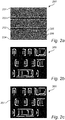
- FIGS 2a-2c illustrate images of a similar pattern as illustrated in figures 1a-1c , in which features may be counted to detect defects according to an embodiment of the present inventive concept.
- the images illustrate a ROI 200, comprising a plurality of features forming a lithographic pattern of a semiconductor wafer.
- Figure 2a illustrates an image as acquired by e.g. a review-SEM
- figure 2b illustrate the image after binarization into black and white, and after features that touch an edge of the image has been removed.
- the horizontal line/space features 201, 202, 203, 204 which all touches one or several edges of the image, has been removed together with features 205, 206 which touches the lower right corner of the image frame. The remaining number of features may then be counted, resulting in 38 features.
- one of the features 207 has broken into two parts, which adds one to the counted number of remaining features.
- the defect pattern of the ROI 200 in figure 2c may be flagged as defect as it contains 39 features instead of the intended number of 38 features as shown in figure 2b .
- FIG. 3 illustrates a test wafer 100, such as e.g. a FEM wafer, used for determination of a process window according to an embodiment of the present inventive concept.
- the test wafer 100 may comprise a plurality of die areas 110 arranged in a matrix of rows and columns.
- the central column may be a modulated focus column, in which the die areas 110 have been provided with a pattern that is printed with incrementally changing de-focus values applied to the lithographic tool (the de-focus may also be achieved by local un-evenness of the wafer surface).
- the central die may represent the zero de-focus position, printed with the best obtainable in-focus of the tool.
- the focus may be shifted increasingly from the zero value, e.g. by average values of +20, +40, +60, +80 and +100 nm above the central die and average values of -20, -40, - 60, -80 and -100 nm below the central die.
- the process window which e.g. may define the limits between which a lithographic parameter, such as e.g. the de-focus value, can vary without resulting in defects, may thus be determined by analysing the quality of the lithographic pattern produced in each one of the dies of the central column.
- the central die comprises a ROI 200 with six features.
- the +60 die one of the features has broken into two separate parts, which results in a total of seven features.
- the defect may be detected by means of a method similar to any of the previously described embodiments.
- the upper de-focus limit for the process window may be determined to +40 nm, if +60 nm is considered as the de-focus value that causes a defect in the pattern.
- a similar approach may be used for detecting hotspots, such as e.g. overlay sensitive hotspots.
- a lithographic pattern may be produced in a semiconductor wafer which may be similarly configured as the test wafer of figure 3 , using a systematically varying overlay between different dies.
- the overlay may e.g. vary in the x-direction (i.e., horizontal direction) in one column, the y-direction (i.e., vertical direction) in another column, and in both the x-direction and the y-direction in a third column.
- the number of features of a particular ROI may then be monitored for the different dies, and defects noted as deviations in the number. When a defect is detected, the particular die may be further analysed to localise exact which feature is failing.
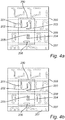
- Figures 4a and 4b are images of a ROI 200 of two different dies on such a wafer.
- features touching the edges of the image may be removed, such that only features 201-206 of figures 4a are counted.
- the ROI therefore comprises six features 201-206.
- Figure 4b is an image of a die which has been printed with an overlay in the y-direction, resulting in a slight translation of the features 201-206 in the vertical direction relative the line/space features 207, 208, 209.
- This vertical shift causes the distance between the lowermost feature 206 and the line feature 207 to be reduced to such extent that the lowermost feature 206 interferes with the line feature 207.
- both features will be removed from the counting and hence excluded from the total number of features. Had the line feature 207 not been removed, had they still been regarded as a single feature and thus counted only once.
- the overlay in the y-direction therefore results in a defect, which is detected as a reduction in the number of counted features from six to five.
- the location of the defect feature 206 may therefore be regarded as a hotspot, which is likely to fail first upon an overlay in the y-direction.
- FIG. 5 is a schematic illustration of a system 500 for detecting defects according to any one of the previously described embodiments.
- the system 500 may comprise an optical analysis tool 530 configured to optically inspect at least some of the dies to locate a ROI and/or a die of interest.
- the ROI or die may comprise a suspected defect, which requires further inspection and analysis.
- the system 500 may further comprise an inspection tool, such as e.g. a scanning electron microscope SEM 510, for acquiring an image of the ROI which may have been determined by the optical analysis tool 530.
- a processing means 520 may be provided for performing the analysis of the acquired image.
- Figure 6 is a schematic representation of a method according an embodiment, which in part or in full may be performed by means of a system according to figure 5 .
- a lithographic pattern is printed 10 on a plurality of die areas of a semiconductor wafer.
- a lithographic parameter such as e.g. dose, focus or overlay, may be varied between different die areas in order to determine a process window and/or hotspot of the pattern.
- the printed lithographic pattern may be optically inspected 20 by e.g. an optical analysis tool. The optical inspection may result in one or several areas, such as e.g. ROIs or die areas, which appear to comprise a defect.
- Those areas may then be subject to a further inspection, in which an image may be acquired 30 by e.g. a SEM in order to detect and/or classify the suspected defect.
- the detection may comprise a step of removing 40, from the image, pattern features that touches an edge of the image, and counting 50 the remaining number of features in the image.
- a statistical analysis 60 of the counted numbers may then be performed, which e.g. may result in a mode number representing the most common number of features in each image. This mode number may be used as a target or reference number, against which the number of features of each image may be compared 70. Deviations from the target number may be flagged 80 as defects.
Landscapes
- General Physics & Mathematics (AREA)
- Physics & Mathematics (AREA)
- Engineering & Computer Science (AREA)
- Health & Medical Sciences (AREA)
- Computer Vision & Pattern Recognition (AREA)
- Immunology (AREA)
- Analytical Chemistry (AREA)
- Pathology (AREA)
- General Health & Medical Sciences (AREA)
- Biochemistry (AREA)
- Life Sciences & Earth Sciences (AREA)
- Chemical & Material Sciences (AREA)
- Quality & Reliability (AREA)
- Theoretical Computer Science (AREA)
- Signal Processing (AREA)
- Public Health (AREA)
- Epidemiology (AREA)
- Environmental & Geological Engineering (AREA)
- Testing Or Measuring Of Semiconductors Or The Like (AREA)
- Exposure And Positioning Against Photoresist Photosensitive Materials (AREA)
- Analysing Materials By The Use Of Radiation (AREA)
Abstract
a) acquiring an image of at least one of said ROIs;
b) removing features touching an edge of said image; and
c) counting the number of remaining features in said image.
Description
- The present inventive concept relates to a method and system for detecting defects of a lithographic pattern used for the production of semiconductor devices.
- Lithography becomes more challenging with the continuous shrink in technology nodes. One attempt to meet the increasing requirements has been to use multiple patterning techniques, in which a pattern is built up by using a plurality of masks per layer. At the same time, the reduced spacing or pitch of the features has led to increasing inspection challenges and defection location detection. Optical inspection tools can give a rough position, but are due to their limited resolution not capable of pin-pointing the exact position within an optical image in which a feature is failing. Review-Scanning Electron Microscope (SEM) may be used for further analysis at the optical defect location, but this is a manual process that is highly time consuming and prone to errors. Another technique utilises E-beam inspection, which also suffer from a low throughput. Thus, there is a need for improved methods for detecting and locating defects.
- An objective of the present inventive concept is to provide an improved method for detecting and locating defects. Further and alternative objectives may be understood from the following.
- The printed lithographic pattern often deviates from the intended lithographic mask design due to errors and phenomena introduced as the pattern is transferred from the mask to the substrate. An important factor affecting the quality of the pattern is the quality and performance of the lithographic tool, which may vary unpredictably due to for example inaccuracies in the tool, wear and environmental changes. The quality of focus and exposure energy (or dose) is of particular interest, wherein the former may be expressed in terms of tolerance with respect to perfect focus (i.e., zero de-focus), resulting in for example a range of de-focus values on either side of the zero de-focus state, and the latter expressed as e.g. a variation in dose. If the deviations in the pattern are large enough to have a detrimental effect on the operation of the intended final structure, they may be referred to as errors or defects.
- Example of errors or defects may include unintended bridging between neighbouring pattern features, e.g. caused by positioning errors, a deviating outline or shape of the features, or contaminating structures arranged between the features. Other examples include cutting or separation of an intended pattern feature into two or more parts. These examples make use of the understanding that a 'feature', in the context of a lithographic pattern, may correspond to an area that forms a continuous shape of the lithographic pattern, i.e., an area that is defined by an uninterrupted and closed outline. Examples of features and possible defects will be discussed in detail in connection with the appended drawings.
- Hence, according to a first aspect of the present inventive concept, there is provided a method for detecting defects of a lithographic pattern on a semiconductor wafer comprising a plurality of die areas. Each of the die areas has a region of interest (ROI), comprising a plurality of features forming the lithographic pattern. The present method involves acquiring an image of at least one of the ROIs, and counting the number of pattern features represented in said image.
- The present inventive concept makes use of the realisation that the number of pattern features represented in an acquired inspection image can be used as an indication of defects, which may be quantified by comparing an actual number of features of an image with a reference number of features. The reference number of features may be obtained in several different ways, such as by statistical analysis of a plurality of images or ROIs, a comparison with a neighbouring ROI or die, or from the design layout file.
- The method may further make use of the fact that the lithographic pattern may be repeated between different dies. By collecting images on a particular and same position within each die, each image may be aligned in similar manner with respect to the lithographic pattern and thus easily compared to each other. Such a comparison may be relatively fast and easy, and any deviation between images of different die areas may be labelled as defects.
- A faster and more reliable analysis of the lithographic pattern is hence provided, not at least since possible defects can be automatically detected without manual inspection and/or analysis by an operator. Further, counting the number of features in each image may require less processing resources as compared to other methods based on analysis of e.g. the outline, shape or area of the pattern features, or on comparing images with each other.
- Advantageously, features touching an edge of the image may be removed from the image prior to the counting of the features. In other words, features not entirely enclosed or included in the image may be excluded from the counting, which thus may include only the number of remaining features in the image. This allows for a more robust defect quantification, as features (or feature edges) arranged at the periphery of the image (or ROI) otherwise may be counted for some images only, depending on positioning errors of the image. If such a feature is visible in a particular image due to a misalignment or positioning error of that image, the feature may erroneously be interpreted as a defect. Similarly, is such a feature is not counted due to the same reason, it may be unintentionally regarded as a failure. Hence, by removing features touching an edge of the image, the accuracy of the method may be increased.
- Further, the removal of features touching an edge of the image also allows for the area of the remaining features to be more accurately analysed. By removing features that do not have their entire area included in the image, the absolute (or relative) area of the remaining features may be better determined or studied. This may e.g. allow for area variations between features of different images, ROIs or dies to be determined and monitored, and possible errors detected or quantified in terms of area deviations.
- In the present context, a 'lithographic pattern' may be defined as a pattern of features or shapes formed on a semiconductor wafer or substrate. The lithographic pattern may be provided by exposing a resist layer, e.g. by direct printing or through a lithographic mask, developing the resist and preferably removing the resist from the exposed or non-exposed areas, depending on the type of resist that is used. This may yield a resist layer in which the features form trenches or lines in the shape of the pattern.
- The terms 'feature', 'shape' or 'component' may refer to a component or area forming the lithographic pattern or the lithographic pattern as reproduced in the image. The pattern as seen on the image may hence be formed of one or several features, which may be subject to image analysis for classification and analysis.
- The lithographic pattern may deviate from the so-called 'design intent' or 'design layout', which may be understood as the theoretical shape of the pattern of features. The actual printed features (for example trenches in a resist layer) may approximate the design intent as much as possible, but deviations may be difficult to avoid due to process parameters related to the printing process.
- The lithographic pattern may be reproduced as an image, acquired by e.g. an inspection tool such as e.g. a scanning electron microscope (SEM). The image may thus be understood as a two-dimensional representation of the lithographic pattern, in which the features of the pattern may appear as two-dimensional shapes in the plane of the image. Advantageously, the image may be binarized, i.e., converted to only black and white, prior to being analysed.
- The area of the pattern that is subject to the defect analysis may be referred to as the region of interest, ROI. The acquired image may coincide with the ROI, or overlap with it. Preferably, the ROI may correspond to a particular position on each die area, such that each ROI comprises (or is intended to comprise) the same set of features. It will however be appreciated that the ROI in some examples also may coincide with the entire die area.
- According to an embodiment, the method may further comprise a step of comparing the number of (remaining) features of the image of the ROI with a target number, or reference number, of features, and a step of flagging the ROI as defect in case the number of features differs from the target number. If the number of counted features exceeds the target number, this may be an indication that one or several of the features comprises a defect in the form of an unintended gap that splits the feature into two or more separate parts. If the number of counted features instead lies below the target number, this may be an indication of a defect in the form of a missing feature or a bridging between two or more features in the image. In both cases, the deviations may be flagged as defects and, possibly, the deviation used as a measure of the severity of the defect.
- In an embodiment, the target number may correspond to the design intent number acquired from the design layout. This may allow for a faster analysis, as defects may be detected as deviations from the design intent number without comparing different images with each other.
- Alternatively, or additionally, the target number may be determined by statistical analysis of a plurality of images. This may e.g. be achieved by counting the number of features of each one of the images, and determining which value, i.e., which number of counted features, that appears most often. This value may also be referred to as the mode number of features, and does hence represent the most common number of features of an image. Assuming that a majority of the images or ROIs contain no detectable defects, those images or ROIs that deviate from the most common number of features may then be defined as defect.
- Using statistical analysis, such as e.g. the mode number described above, makes the present method suitable also in cases when the design intent number is unknown. Thus, the method may be used for analysing any type of repeating lithographic pattern, given that access is given to a plurality of images of the same position within each die.
- The present inventive concept may further be employed when estimating a process window of the features. A process window may define the printability performance limits in terms of e.g. focus and dose settings of a lithographic printing tool, within which limits a reliable print of the pattern is obtainable. Some patterns or features can have a larger process window than others, due to various reasons such as design geometry and optical phenomena taking place during the exposure. Particularly sensitive areas of the pattern, which are likely to be printed incorrectly due to e.g. certain geometrical parameters of the design and their interaction with optical phenomena occurring during the exposure of the mask, are sometimes referred to as hotspots. It may therefore be of particular interest to determine the process window for those areas.
- Thus, according to an embodiment, the method may comprise a step of printing, by a lithographic tool, the lithographic pattern on the plurality of die areas, while varying a lithographic parameter between different die areas. The number of features in each die area may then be determined as a function of the lithographic parameter, and a process window determined as the limits between which the lithographic parameter can vary without the number of features deviates from a target number of features. The lithographic parameter may be at least one of dose, focus and overlay, which may be varied so as to determine at which parameter offset a particular feature (or any feature) or hotspot starts failing by showing a change in the number of components. Further, this approach may be used to understand at which position within a feature the failure tends to occur, which may be used to guide e.g. CD-SEMs to the exact location for automatic measurement gauge setup.
- In one example, the process window may be estimated by means of a test wafer, such as e.g. a Critical Dimension Uniformity (CDU) wafer or a Focus Exposure energy Matrix (FEM) wafer. The test wafer may comprise a plurality of die areas arranged in rows and columns. The central column of dies may e.g. be a modulated focus column, representing die areas where a particular pattern is printed with incrementally changing de-focus values deliberately applied in the lithographic printing tool. The central die may represent the zero de-focus position of the lithographic mask with respect to the wafer, i.e., the best obtainable in-focus print of the die. Above and underneath the central die, de-focused prints may be produced at incrementally increasing de-focus values on either side of the zero value, in steps of e.g. +10 nm and -10 nm, obtained by e.g. displacing the lens assembly of the tool in steps with respect to the zero de-focus position, or by displacing the wafer stage with respect to the lens assembly. The rest of the dies in the wafer (outside the central column) may be zero de-focus dies, but could also be additional de-focused prints. Preferably, a zero de-focused column may be printed next to a modulated focus column in order to facilitate the detection of defects by comparing the number of features of two dies of adjacent columns.
- According to some embodiments, a position of the ROIs may be located prior to the image is acquired. This may e.g. be achieved by extracting hotspots from the design layout and use these for the subsequent detection of defects. In another example, the position of the ROIs may be determined by means of optical inspection of at least some of the dies. Even though the optical inspection may have a too low resolution or accuracy to efficiently locate or classify a defect, the average deviation of the intensity pattern of the optical image (e.g. as compared to other images of corresponding locations of other dies) may be used to detect that there may be a defect within the ROI. Thus, the optical inspection may be completed with an additional, a more thorough inspection according to the present inventive concept. The optical inspection may be performed as an initial step for detecting specific ROIs within a die that should be further inspected for defects, or for detecting specific dies that should be further checked.
- Thus, the present inventive concept may be realised by an initial inspection by an optical inspection tool, which can give a rough position of a suspected defect. A subsequent inspection, e.g. by means of a review SEM, may then be performed at the suspected defect location, and the acquired images analysed according to the above described embodiments.
- In one example, hotspots or specific feature locations in which defects are likely to occur first, may be determined by means of e.g. the test wafer as discussed above, or by means of post-processing of the acquired images. Examples of such techniques may e.g. include dilation and erosion, by which the features of the images are gradually and systematically distorted until the number of features changes. In erosion techniques, one pixel at the time may be removed from the boundary of the feature, until the feature is counted as two separate features. In dilation techniques, the pixels are gradually added to the boundary until two features eventually merges into one. Dilation or erosion can then be used to find a specific location or feature, within the ROI, which is failing. Once that location or feature is known, the design layout may be used for determining how many times this feature or location is repeating. Based on this information, optical inspection may be performed on those particular sites of the design. In other words, the specific locations may be inspected and analysed across the die, which may reduce random noise and makes the optical inspection tool more sensitive, since it is looking at a specific type of feature. Thus, SEM tools may be used for finding which feature is failing within a ROI, wherein this information is used as feedback to the optical inspection tool for generating similar areas from the design layout and running a full die inspection for these areas.
- According to an embodiment, the step of removing features touching an edge of the image may include removing all such features except line/space features having no more than one intended line-end position positioned within the image. In that way, the present inventive concept may be utilised for detecting defects (such as bridges and cuts) also in line/space patterns.
- According to a second aspect, a system may be provided for carrying out the method according to the first aspect. The system may comprise a SEM for acquiring the image and processing means for counting the number of features in the image. The processing means may further be configured to remove features touching an edge of the image.
- In an embodiment, the system also comprises an optical analysis tool for optically inspecting at least some of the dies to locate a position of the ROIs, and/or to determine a die of interest that should be subject to further and more detailed inspection.
- Either of the SEM, the optical analysis tool and the processing means may be structurally integrated in the system. They may also be structurally distinct, i.e. physically separated and/or located on different geographical positions, even if connected or being connectable to each other via e.g. a communication network.
- The processing means may include a processor or any other electrical circuitry capable of performing the required image analysis. The physical implementation may e.g. be an integrated implementation, or a distributed implementation in which the responsibilities and functionalities are handled by cooperating components.
- The inventive concept disclosed may be embodied as computer readable instructions for controlling a programmable computer in such manner that it causes an inspection tool or a system as described above to perform the methods outlined above. Such instructions may be distributed in the form of a computer program product comprising a non-volatile computer-readable medium storing the instructions.
- It is noted that the present inventive concept relates to all possible combinations of features recited in the claims. Further, it will be appreciated that the various embodiments described for the method according to the first aspect are all combinable with embodiments described for the system according to the second aspect. Further objectives of, features of, and advantages with the present inventive concept will become apparent when studying the following detailed disclosure, the drawings, and the appended claims. Those skilled in the art will realise that different features of the present invention can be combined to create embodiments other than those described in the following
- The above, as well as additional objects, features and advantages of the present inventive concept, will be better understood through the following illustrative and non-limiting detailed description of embodiments of the present inventive concept, with reference to the appended drawings.
-
Figures 1a-1c show images of a ROI comprising a plurality of features of a lithographic pattern. -
Figures 2a-2c show images of a ROI, in which some features are removed prior to counting. -
Figure 3 is a schematic layout of a semiconductor wafer, comprising a plurality of die areas printed with different lithographic parameter settings according to an embodiment. -
Figures 4a and 4b illustrate a ROI of an image and the detection of a hotspot according to an embodiment. -
Figure 5 is a schematic illustration of a system according to an embodiment. -
Figure 6 is a diagram illustrating a method for detecting defects of a lithographic pattern on a semiconductor wafer according to an embodiment of the present inventive concept. - As illustrated in the figures, the size of the elements, features and other structures may be exaggerated or not depcited proportionally for illustrative purposes. Thus, the figures are provided to illustrate the general elements of the embodiments.
- The present inventive concept is concerned with analysis of defects that may occur in lithographic pattern. Example of such defects will be described in the following with reference to
figures 1a-1c , which illustrate three different images taken at the same position within three different dies of a patterned semiconductor wafer. The images may be considered to illustrate the features 201-206 included in anROI 200 of the respective dies. The images may e.g. be acquired by an inspection tool, such as e.g. a SEM. - As shown in
figure 1a , the lithographic pattern of theROI 200 may comprise six features or components 201-206, in this example two pairs ofvertical lines brackets figure 1 a is considered to not comprise any defects, the number of features 201-206 (in this case six) of theROI 200 may be referred to as a reference number or target for the number of features within this particular ROI of the pattern. - In
figure 1b , it is noted that the vertical line-shapedfeature 202 comprises a defect, realised as a cut into two separate parts - a first, upper part and a second, lower part. When counting the number of features, this cut results in a total number of seven features 201-206 in theROI 200. Thus, when comparing to the reference number, or intended number of features or components infigure 1a , thefeature 202 offigure 1b can be defined as defect. - A similar analysis can be employed to the
ROI 200 offigure 1c , in which thefeature 205 has been bridged or merged withfeature 206. Thus, the number of features infigure 1c has been reduced to five and can therefore be regarded as defect when compared with the reference offigure 1a . - It will be understood that the present examples are merely illustrations of two possible printing error or pattern defects. Other types of defects, resulting in a deviating number of features, are however equally conceivable. The counted number of features may be compared to a target number of features, such as the features of a defect-free ROI as described with reference to
figures 1a-1c . The target number may however also be retrieved e.g. from the design layout, be determined manually by an operator, or statistically as e.g. a mode number of a plurality of images. -
Figures 2a-2c illustrate images of a similar pattern as illustrated infigures 1a-1c , in which features may be counted to detect defects according to an embodiment of the present inventive concept. The images illustrate aROI 200, comprising a plurality of features forming a lithographic pattern of a semiconductor wafer. -
Figure 2a illustrates an image as acquired by e.g. a review-SEM, whereasfigure 2b illustrate the image after binarization into black and white, and after features that touch an edge of the image has been removed. Thus, the horizontal line/space features 201, 202, 203, 204, which all touches one or several edges of the image, has been removed together withfeatures - In
figure 2c , one of thefeatures 207 has broken into two parts, which adds one to the counted number of remaining features. Thus, the defect pattern of theROI 200 infigure 2c may be flagged as defect as it contains 39 features instead of the intended number of 38 features as shown infigure 2b . -
Figure 3 illustrates atest wafer 100, such as e.g. a FEM wafer, used for determination of a process window according to an embodiment of the present inventive concept. Thetest wafer 100 may comprise a plurality ofdie areas 110 arranged in a matrix of rows and columns. In the present example, the central column may be a modulated focus column, in which thedie areas 110 have been provided with a pattern that is printed with incrementally changing de-focus values applied to the lithographic tool (the de-focus may also be achieved by local un-evenness of the wafer surface). The central die may represent the zero de-focus position, printed with the best obtainable in-focus of the tool. Above and underneath the central die, the focus may be shifted increasingly from the zero value, e.g. by average values of +20, +40, +60, +80 and +100 nm above the central die and average values of -20, -40, - 60, -80 and -100 nm below the central die. - The process window, which e.g. may define the limits between which a lithographic parameter, such as e.g. the de-focus value, can vary without resulting in defects, may thus be determined by analysing the quality of the lithographic pattern produced in each one of the dies of the central column. As illustrated in the example of
figure 3 , the central die comprises aROI 200 with six features. In the +60 die, one of the features has broken into two separate parts, which results in a total of seven features. The defect may be detected by means of a method similar to any of the previously described embodiments. In this way, the upper de-focus limit for the process window may be determined to +40 nm, if +60 nm is considered as the de-focus value that causes a defect in the pattern. - A similar approach may be used for detecting hotspots, such as e.g. overlay sensitive hotspots. A lithographic pattern may be produced in a semiconductor wafer which may be similarly configured as the test wafer of
figure 3 , using a systematically varying overlay between different dies. The overlay may e.g. vary in the x-direction (i.e., horizontal direction) in one column, the y-direction (i.e., vertical direction) in another column, and in both the x-direction and the y-direction in a third column. The number of features of a particular ROI may then be monitored for the different dies, and defects noted as deviations in the number. When a defect is detected, the particular die may be further analysed to localise exact which feature is failing. -
Figures 4a and 4b are images of aROI 200 of two different dies on such a wafer. In this example, features touching the edges of the image may be removed, such that only features 201-206 offigures 4a are counted. In the present example, the ROI therefore comprises six features 201-206. -
Figure 4b is an image of a die which has been printed with an overlay in the y-direction, resulting in a slight translation of the features 201-206 in the vertical direction relative the line/space features 207, 208, 209. This vertical shift causes the distance between thelowermost feature 206 and theline feature 207 to be reduced to such extent that thelowermost feature 206 interferes with theline feature 207. As illustrated in the image offigure 4b , they now appear to be connected or bridged, and are therefore regarded as a single feature. As a result, both features will be removed from the counting and hence excluded from the total number of features. Had theline feature 207 not been removed, had they still been regarded as a single feature and thus counted only once. - The overlay in the y-direction therefore results in a defect, which is detected as a reduction in the number of counted features from six to five. The location of the
defect feature 206 may therefore be regarded as a hotspot, which is likely to fail first upon an overlay in the y-direction. - It is appreciated that the above embodiments discussed in connection with
figures 3 and4a-b merely are illustrative examples of advantageous applications and uses of the present inventive concept for determining process window and hotspots. The skilled person however realises that many other variations and combinations are conceivable within the scope of the claimed embodiments. -
Figure 5 is a schematic illustration of asystem 500 for detecting defects according to any one of the previously described embodiments. Thesystem 500 may comprise anoptical analysis tool 530 configured to optically inspect at least some of the dies to locate a ROI and/or a die of interest. The ROI or die may comprise a suspected defect, which requires further inspection and analysis. For this purpose, thesystem 500 may further comprise an inspection tool, such as e.g. a scanningelectron microscope SEM 510, for acquiring an image of the ROI which may have been determined by theoptical analysis tool 530. Further, a processing means 520 may be provided for performing the analysis of the acquired image. -
Figure 6 is a schematic representation of a method according an embodiment, which in part or in full may be performed by means of a system according tofigure 5 . In a first step, a lithographic pattern is printed 10 on a plurality of die areas of a semiconductor wafer. During the printing, a lithographic parameter, such as e.g. dose, focus or overlay, may be varied between different die areas in order to determine a process window and/or hotspot of the pattern. The printed lithographic pattern may be optically inspected 20 by e.g. an optical analysis tool. The optical inspection may result in one or several areas, such as e.g. ROIs or die areas, which appear to comprise a defect. Those areas may then be subject to a further inspection, in which an image may be acquired 30 by e.g. a SEM in order to detect and/or classify the suspected defect. The detection may comprise a step of removing 40, from the image, pattern features that touches an edge of the image, and counting 50 the remaining number of features in the image. Astatistical analysis 60 of the counted numbers may then be performed, which e.g. may result in a mode number representing the most common number of features in each image. This mode number may be used as a target or reference number, against which the number of features of each image may be compared 70. Deviations from the target number may be flagged 80 as defects. - In the above the inventive concept has mainly been described with reference to a limited number of examples. However, as is readily appreciated by a person skilled in the art, other examples than the ones disclosed above are equally possible within the scope of the inventive concept, as defined by the appended claims. Variations to the disclosed embodiments may be understood and effected by the skilled person in practising the inventive concept, from a study of the drawings, the disclosure and the appended claims.
Claims (15)
- A method for detecting defects of a lithographic pattern on a semiconductor wafer (100) comprising a plurality of die areas (110), wherein each of the die areas has a region of interest, ROI (200), comprising a plurality of features (201-209) forming the lithographic pattern, wherein the method comprises the following steps:a) acquiring (30) an image of at least one of said ROIs;b) removing (40) features touching an edge of said image; andc) counting (50) the number of remaining features in said image.
- The method according to claim 1, further comprising:comparing (70) said number of remaining features of said image of the ROI with a target number of features;flagging (80) said ROI as defect in case the number of remaining features in said image differs from said target number.
- The method according to claim 2, wherein the target number is the design intent number of features of the design layout.
- The method according to claim 1, comprising:acquiring an image of each one of a plurality of ROIs;determining (60), for each image, the number of remaining features by performing steps b) and c);determining a mode number of features for the images of the plurality of ROIs; andfor each image:comparing the number of remaining features of said image with said mode number; andflagging the ROI associated with said image as defect in case the number of features differ from said mode number.
- The method according to claim 1, further comprising the steps of:printing (10), by a lithographic tool, the lithographic pattern on said plurality of die areas, wherein a lithographic parameter is varied between different die areas;determining the number of remaining features in each die area as a function of the corresponding lithographic parameter; anddetermining, based on said number of remaining features, a process window defining limits between which said lithographic parameter can vary without said number of features deviating from a target number of features.
- The method according to claim 5, wherein the lithographic parameter is at least one of dose, focus and overlay.
- The method according to claim 1, wherein, prior to step a), a position of the ROIs is located by extracting hotspots from the design layout.
- The method according to claim 1, wherein, prior to step a), a position of the ROIs is located by means of optical inspection of at least some of the dies.
- The method according to claim 1, wherein, prior to step a), a die of interest is determined (20) by means of optical inspection of at least some of the dies.
- The method according to claim 1, wherein step b) comprises removing features touching an edge of said image, with the exception of line/space features having no more than one intended line-end position within the image.
- The method according to claim 1, wherein said image is acquired by means of a scanning electron microscope, SEM.
- The method according to claim 1, wherein the image is binarized prior to step b).
- A system (500) for detecting defects of a lithographic pattern on a semiconductor wafer (100) comprising a plurality of die areas (110), wherein each of the die areas has a region of interest, ROI (200), comprising a plurality of features (201-209) forming the lithographic pattern, wherein the system comprises:a scanning electron microscope, SEM (510), for acquiring an image of at least one of said ROIs;processing means (520) for removing features touching an edge of said image; andprocessing means for counting the number of remaining features in said image.
- The system according to claim 13, wherein the system further comprises an optical analysis tool (530) configured to optically inspect at least some of the dies to locate a position the ROIs.
- The system according to claim 13, wherein the system further comprises an optical analysis tool configured to optically inspect at least some of the dies to determine a die of interest.
Priority Applications (3)
| Application Number | Priority Date | Filing Date | Title |
|---|---|---|---|
| EP17190509.4A EP3454128B1 (en) | 2017-09-12 | 2017-09-12 | A method and system for detecting defects of a lithographic pattern |
| US16/125,107 US10732124B2 (en) | 2017-09-12 | 2018-09-07 | Methods for detecting defects of a lithographic pattern |
| CN201811063017.6A CN109491210B (en) | 2017-09-12 | 2018-09-12 | A method and system for detecting defects in lithographic patterns |
Applications Claiming Priority (1)
| Application Number | Priority Date | Filing Date | Title |
|---|---|---|---|
| EP17190509.4A EP3454128B1 (en) | 2017-09-12 | 2017-09-12 | A method and system for detecting defects of a lithographic pattern |
Publications (2)
| Publication Number | Publication Date |
|---|---|
| EP3454128A1 true EP3454128A1 (en) | 2019-03-13 |
| EP3454128B1 EP3454128B1 (en) | 2020-01-29 |
Family
ID=59856427
Family Applications (1)
| Application Number | Title | Priority Date | Filing Date |
|---|---|---|---|
| EP17190509.4A Active EP3454128B1 (en) | 2017-09-12 | 2017-09-12 | A method and system for detecting defects of a lithographic pattern |
Country Status (3)
| Country | Link |
|---|---|
| US (1) | US10732124B2 (en) |
| EP (1) | EP3454128B1 (en) |
| CN (1) | CN109491210B (en) |
Cited By (1)
| Publication number | Priority date | Publication date | Assignee | Title |
|---|---|---|---|---|
| CN113009789A (en) * | 2021-03-05 | 2021-06-22 | 广东省大湾区集成电路与系统应用研究院 | Potential hot spot pattern area determining method and photoetching hot spot pattern obtaining method |
Families Citing this family (4)
| Publication number | Priority date | Publication date | Assignee | Title |
|---|---|---|---|---|
| US11145526B2 (en) * | 2018-09-27 | 2021-10-12 | Taiwan Semiconductor Manufacturing Company Ltd. | Method of analyzing a manufacturing of a semiconductor structure |
| US11282189B2 (en) * | 2019-09-16 | 2022-03-22 | Intel Corporation | Unsupervised clustering to identify anomalies |
| CN116157708B (en) * | 2020-07-20 | 2026-03-31 | 应用材料公司 | Optical devices and methods of measuring optical devices |
| CN112330678B (en) * | 2021-01-07 | 2021-04-02 | 中科慧远视觉技术(北京)有限公司 | Product edge defect detection method |
Citations (2)
| Publication number | Priority date | Publication date | Assignee | Title |
|---|---|---|---|---|
| JP2010170002A (en) * | 2009-01-26 | 2010-08-05 | Toppan Printing Co Ltd | Method and apparatus for inspecting pattern |
| US20170160648A1 (en) * | 2014-07-21 | 2017-06-08 | Asml Netherlands B.V. | Method for determining a process window for a lithographic process, associated apparatuses and a computer program |
Family Cites Families (17)
| Publication number | Priority date | Publication date | Assignee | Title |
|---|---|---|---|---|
| JP4206192B2 (en) | 2000-11-09 | 2009-01-07 | 株式会社日立製作所 | Pattern inspection method and apparatus |
| US6836560B2 (en) * | 2000-11-13 | 2004-12-28 | Kla - Tencor Technologies Corporation | Advanced phase shift inspection method |
| US7608468B1 (en) * | 2003-07-02 | 2009-10-27 | Kla-Tencor Technologies, Corp. | Apparatus and methods for determining overlay and uses of same |
| US9710903B2 (en) | 2008-06-11 | 2017-07-18 | Kla-Tencor Corp. | System and method for detecting design and process defects on a wafer using process monitoring features |
| US20110296362A1 (en) * | 2009-02-04 | 2011-12-01 | Tamao Ishikawa | Semiconductor defect integrated projection method and defect inspection support apparatus equipped with semiconductor defect integrated projection function |
| JP2013055197A (en) * | 2011-09-02 | 2013-03-21 | Toshiba Corp | Exposure method and exposure mask |
| CN102566322B (en) * | 2012-02-28 | 2014-05-28 | 上海华力微电子有限公司 | Multiple photoetching equipment correcting method |
| US9202763B2 (en) * | 2013-01-16 | 2015-12-01 | Kabushiki Kaisha Toshiba | Defect pattern evaluation method, defect pattern evaluation apparatus, and recording media |
| KR102019534B1 (en) | 2013-02-01 | 2019-09-09 | 케이엘에이 코포레이션 | Detecting defects on a wafer using defect-specific and multi-channel information |
| US9990708B2 (en) * | 2013-02-20 | 2018-06-05 | Hitachi High-Technologies Corporation | Pattern-measuring apparatus and semiconductor-measuring system |
| JP6043662B2 (en) * | 2013-03-18 | 2016-12-14 | 株式会社ニューフレアテクノロジー | Inspection method and inspection apparatus |
| JP6170707B2 (en) * | 2013-04-01 | 2017-07-26 | 株式会社ニューフレアテクノロジー | Inspection method and inspection apparatus |
| KR102085522B1 (en) * | 2013-11-14 | 2020-03-06 | 삼성전자 주식회사 | Method for detecting the defect of the pattern |
| US9518934B2 (en) * | 2014-11-04 | 2016-12-13 | Kla-Tencor Corp. | Wafer defect discovery |
| WO2016128189A1 (en) * | 2015-02-13 | 2016-08-18 | Asml Netherlands B.V. | Process variability aware adaptive inspection and metrology |
| US9846934B2 (en) * | 2015-04-13 | 2017-12-19 | Anchor Semiconductor Inc. | Pattern weakness and strength detection and tracking during a semiconductor device fabrication process |
| US9910348B2 (en) * | 2015-06-30 | 2018-03-06 | Globalfoundries Inc. | Method of simultaneous lithography and etch correction flow |
-
2017
- 2017-09-12 EP EP17190509.4A patent/EP3454128B1/en active Active
-
2018
- 2018-09-07 US US16/125,107 patent/US10732124B2/en active Active
- 2018-09-12 CN CN201811063017.6A patent/CN109491210B/en active Active
Patent Citations (2)
| Publication number | Priority date | Publication date | Assignee | Title |
|---|---|---|---|---|
| JP2010170002A (en) * | 2009-01-26 | 2010-08-05 | Toppan Printing Co Ltd | Method and apparatus for inspecting pattern |
| US20170160648A1 (en) * | 2014-07-21 | 2017-06-08 | Asml Netherlands B.V. | Method for determining a process window for a lithographic process, associated apparatuses and a computer program |
Cited By (1)
| Publication number | Priority date | Publication date | Assignee | Title |
|---|---|---|---|---|
| CN113009789A (en) * | 2021-03-05 | 2021-06-22 | 广东省大湾区集成电路与系统应用研究院 | Potential hot spot pattern area determining method and photoetching hot spot pattern obtaining method |
Also Published As
| Publication number | Publication date |
|---|---|
| CN109491210B (en) | 2021-07-23 |
| US10732124B2 (en) | 2020-08-04 |
| US20190079023A1 (en) | 2019-03-14 |
| EP3454128B1 (en) | 2020-01-29 |
| CN109491210A (en) | 2019-03-19 |
Similar Documents
| Publication | Publication Date | Title |
|---|---|---|
| US10732124B2 (en) | Methods for detecting defects of a lithographic pattern | |
| JP6320387B2 (en) | Device correlation measurement method (DCM) for OVL with embedded SEM structure overlay target | |
| US7760347B2 (en) | Design-based method for grouping systematic defects in lithography pattern writing system | |
| KR100979484B1 (en) | Defect investigation method including obtaining a virtual image of a reticle for other lithographic process variables | |
| TWI517210B (en) | Pattern evaluation method and pattern evaluation device | |
| EP2317388A2 (en) | Method and system for wafer inspection | |
| JP5543984B2 (en) | CD measurement system and method for classifying similar structural elements | |
| US20130279793A1 (en) | Image processing apparatus and computer program | |
| US20040009416A1 (en) | Qualifying patterns, patterning processes, or patterning apparatus in the fabrication of microlithographic patterns | |
| TW201504622A (en) | Pattern measuring device, and semiconductor measuring system | |
| JP2009222454A (en) | Pattern measuring method and device | |
| JP5192795B2 (en) | Electron beam measuring device | |
| US20140205180A1 (en) | Method, apparatus and device for inspecting circuit pattern defect | |
| US9874821B2 (en) | Method for hotspot detection and ranking of a lithographic mask | |
| KR102447609B1 (en) | Computer-assisted weak pattern detection and quantification system | |
| US9983154B2 (en) | Method for inspecting a pattern of features on a semiconductor die | |
| CN107831638B (en) | Method for detecting pollution of contact surface of mask and mask table | |
| CN106610564B (en) | Inspection method and inspection system for exposure process and mask testing plate | |
| CN119689792A (en) | Detection method of SRAF development defects | |
| KR20100073374A (en) | Method for detecting defects of semiconductor device | |
| KR20100034611A (en) | Method for verification of process window in semiconductor device | |
| Strozewski et al. | A new methodology to specify via and contact layer reticles for maximizing process latitude | |
| KR20080001734A (en) | How to Check for Mask Defect Locations | |
| KR20080093201A (en) | How to prevent errors in mask pattern checking |
Legal Events
| Date | Code | Title | Description |
|---|---|---|---|
| PUAI | Public reference made under article 153(3) epc to a published international application that has entered the european phase |
Free format text: ORIGINAL CODE: 0009012 |
|
| STAA | Information on the status of an ep patent application or granted ep patent |
Free format text: STATUS: THE APPLICATION HAS BEEN PUBLISHED |
|
| AK | Designated contracting states |
Kind code of ref document: A1 Designated state(s): AL AT BE BG CH CY CZ DE DK EE ES FI FR GB GR HR HU IE IS IT LI LT LU LV MC MK MT NL NO PL PT RO RS SE SI SK SM TR |
|
| AX | Request for extension of the european patent |
Extension state: BA ME |
|
| STAA | Information on the status of an ep patent application or granted ep patent |
Free format text: STATUS: REQUEST FOR EXAMINATION WAS MADE |
|
| 17P | Request for examination filed |
Effective date: 20190610 |
|
| RBV | Designated contracting states (corrected) |
Designated state(s): AL AT BE BG CH CY CZ DE DK EE ES FI FR GB GR HR HU IE IS IT LI LT LU LV MC MK MT NL NO PL PT RO RS SE SI SK SM TR |
|
| GRAP | Despatch of communication of intention to grant a patent |
Free format text: ORIGINAL CODE: EPIDOSNIGR1 |
|
| STAA | Information on the status of an ep patent application or granted ep patent |
Free format text: STATUS: GRANT OF PATENT IS INTENDED |
|
| RIC1 | Information provided on ipc code assigned before grant |
Ipc: G06T 7/00 20170101ALI20191022BHEP Ipc: G03F 7/20 20060101AFI20191022BHEP Ipc: G01N 21/956 20060101ALI20191022BHEP Ipc: G01N 21/88 20060101ALI20191022BHEP |
|
| INTG | Intention to grant announced |
Effective date: 20191114 |
|
| GRAS | Grant fee paid |
Free format text: ORIGINAL CODE: EPIDOSNIGR3 |
|
| GRAA | (expected) grant |
Free format text: ORIGINAL CODE: 0009210 |
|
| STAA | Information on the status of an ep patent application or granted ep patent |
Free format text: STATUS: THE PATENT HAS BEEN GRANTED |
|
| AK | Designated contracting states |
Kind code of ref document: B1 Designated state(s): AL AT BE BG CH CY CZ DE DK EE ES FI FR GB GR HR HU IE IS IT LI LT LU LV MC MK MT NL NO PL PT RO RS SE SI SK SM TR |
|
| REG | Reference to a national code |
Ref country code: GB Ref legal event code: FG4D |
|
| REG | Reference to a national code |
Ref country code: CH Ref legal event code: EP |
|
| REG | Reference to a national code |
Ref country code: AT Ref legal event code: REF Ref document number: 1228905 Country of ref document: AT Kind code of ref document: T Effective date: 20200215 |
|
| REG | Reference to a national code |
Ref country code: IE Ref legal event code: FG4D |
|
| REG | Reference to a national code |
Ref country code: DE Ref legal event code: R096 Ref document number: 602017011123 Country of ref document: DE |
|
| REG | Reference to a national code |
Ref country code: NL Ref legal event code: MP Effective date: 20200129 |
|
| PG25 | Lapsed in a contracting state [announced via postgrant information from national office to epo] |
Ref country code: RS Free format text: LAPSE BECAUSE OF FAILURE TO SUBMIT A TRANSLATION OF THE DESCRIPTION OR TO PAY THE FEE WITHIN THE PRESCRIBED TIME-LIMIT Effective date: 20200129 Ref country code: FI Free format text: LAPSE BECAUSE OF FAILURE TO SUBMIT A TRANSLATION OF THE DESCRIPTION OR TO PAY THE FEE WITHIN THE PRESCRIBED TIME-LIMIT Effective date: 20200129 Ref country code: PT Free format text: LAPSE BECAUSE OF FAILURE TO SUBMIT A TRANSLATION OF THE DESCRIPTION OR TO PAY THE FEE WITHIN THE PRESCRIBED TIME-LIMIT Effective date: 20200621 Ref country code: NO Free format text: LAPSE BECAUSE OF FAILURE TO SUBMIT A TRANSLATION OF THE DESCRIPTION OR TO PAY THE FEE WITHIN THE PRESCRIBED TIME-LIMIT Effective date: 20200429 |
|
| REG | Reference to a national code |
Ref country code: LT Ref legal event code: MG4D |
|
| PG25 | Lapsed in a contracting state [announced via postgrant information from national office to epo] |
Ref country code: SE Free format text: LAPSE BECAUSE OF FAILURE TO SUBMIT A TRANSLATION OF THE DESCRIPTION OR TO PAY THE FEE WITHIN THE PRESCRIBED TIME-LIMIT Effective date: 20200129 Ref country code: HR Free format text: LAPSE BECAUSE OF FAILURE TO SUBMIT A TRANSLATION OF THE DESCRIPTION OR TO PAY THE FEE WITHIN THE PRESCRIBED TIME-LIMIT Effective date: 20200129 Ref country code: LV Free format text: LAPSE BECAUSE OF FAILURE TO SUBMIT A TRANSLATION OF THE DESCRIPTION OR TO PAY THE FEE WITHIN THE PRESCRIBED TIME-LIMIT Effective date: 20200129 Ref country code: IS Free format text: LAPSE BECAUSE OF FAILURE TO SUBMIT A TRANSLATION OF THE DESCRIPTION OR TO PAY THE FEE WITHIN THE PRESCRIBED TIME-LIMIT Effective date: 20200529 Ref country code: BG Free format text: LAPSE BECAUSE OF FAILURE TO SUBMIT A TRANSLATION OF THE DESCRIPTION OR TO PAY THE FEE WITHIN THE PRESCRIBED TIME-LIMIT Effective date: 20200429 Ref country code: GR Free format text: LAPSE BECAUSE OF FAILURE TO SUBMIT A TRANSLATION OF THE DESCRIPTION OR TO PAY THE FEE WITHIN THE PRESCRIBED TIME-LIMIT Effective date: 20200430 |
|
| PG25 | Lapsed in a contracting state [announced via postgrant information from national office to epo] |
Ref country code: NL Free format text: LAPSE BECAUSE OF FAILURE TO SUBMIT A TRANSLATION OF THE DESCRIPTION OR TO PAY THE FEE WITHIN THE PRESCRIBED TIME-LIMIT Effective date: 20200129 |
|
| PG25 | Lapsed in a contracting state [announced via postgrant information from national office to epo] |
Ref country code: CZ Free format text: LAPSE BECAUSE OF FAILURE TO SUBMIT A TRANSLATION OF THE DESCRIPTION OR TO PAY THE FEE WITHIN THE PRESCRIBED TIME-LIMIT Effective date: 20200129 Ref country code: RO Free format text: LAPSE BECAUSE OF FAILURE TO SUBMIT A TRANSLATION OF THE DESCRIPTION OR TO PAY THE FEE WITHIN THE PRESCRIBED TIME-LIMIT Effective date: 20200129 Ref country code: SK Free format text: LAPSE BECAUSE OF FAILURE TO SUBMIT A TRANSLATION OF THE DESCRIPTION OR TO PAY THE FEE WITHIN THE PRESCRIBED TIME-LIMIT Effective date: 20200129 Ref country code: LT Free format text: LAPSE BECAUSE OF FAILURE TO SUBMIT A TRANSLATION OF THE DESCRIPTION OR TO PAY THE FEE WITHIN THE PRESCRIBED TIME-LIMIT Effective date: 20200129 Ref country code: ES Free format text: LAPSE BECAUSE OF FAILURE TO SUBMIT A TRANSLATION OF THE DESCRIPTION OR TO PAY THE FEE WITHIN THE PRESCRIBED TIME-LIMIT Effective date: 20200129 Ref country code: EE Free format text: LAPSE BECAUSE OF FAILURE TO SUBMIT A TRANSLATION OF THE DESCRIPTION OR TO PAY THE FEE WITHIN THE PRESCRIBED TIME-LIMIT Effective date: 20200129 Ref country code: SM Free format text: LAPSE BECAUSE OF FAILURE TO SUBMIT A TRANSLATION OF THE DESCRIPTION OR TO PAY THE FEE WITHIN THE PRESCRIBED TIME-LIMIT Effective date: 20200129 Ref country code: DK Free format text: LAPSE BECAUSE OF FAILURE TO SUBMIT A TRANSLATION OF THE DESCRIPTION OR TO PAY THE FEE WITHIN THE PRESCRIBED TIME-LIMIT Effective date: 20200129 |
|
| REG | Reference to a national code |
Ref country code: DE Ref legal event code: R097 Ref document number: 602017011123 Country of ref document: DE |
|
| REG | Reference to a national code |
Ref country code: AT Ref legal event code: MK05 Ref document number: 1228905 Country of ref document: AT Kind code of ref document: T Effective date: 20200129 |
|
| PLBE | No opposition filed within time limit |
Free format text: ORIGINAL CODE: 0009261 |
|
| STAA | Information on the status of an ep patent application or granted ep patent |
Free format text: STATUS: NO OPPOSITION FILED WITHIN TIME LIMIT |
|
| 26N | No opposition filed |
Effective date: 20201030 |
|
| PG25 | Lapsed in a contracting state [announced via postgrant information from national office to epo] |
Ref country code: AT Free format text: LAPSE BECAUSE OF FAILURE TO SUBMIT A TRANSLATION OF THE DESCRIPTION OR TO PAY THE FEE WITHIN THE PRESCRIBED TIME-LIMIT Effective date: 20200129 Ref country code: IT Free format text: LAPSE BECAUSE OF FAILURE TO SUBMIT A TRANSLATION OF THE DESCRIPTION OR TO PAY THE FEE WITHIN THE PRESCRIBED TIME-LIMIT Effective date: 20200129 |
|
| PG25 | Lapsed in a contracting state [announced via postgrant information from national office to epo] |
Ref country code: SI Free format text: LAPSE BECAUSE OF FAILURE TO SUBMIT A TRANSLATION OF THE DESCRIPTION OR TO PAY THE FEE WITHIN THE PRESCRIBED TIME-LIMIT Effective date: 20200129 Ref country code: PL Free format text: LAPSE BECAUSE OF FAILURE TO SUBMIT A TRANSLATION OF THE DESCRIPTION OR TO PAY THE FEE WITHIN THE PRESCRIBED TIME-LIMIT Effective date: 20200129 |
|
| REG | Reference to a national code |
Ref country code: CH Ref legal event code: PL |
|
| REG | Reference to a national code |
Ref country code: BE Ref legal event code: MM Effective date: 20200930 |
|
| PG25 | Lapsed in a contracting state [announced via postgrant information from national office to epo] |
Ref country code: LU Free format text: LAPSE BECAUSE OF NON-PAYMENT OF DUE FEES Effective date: 20200912 |
|
| PG25 | Lapsed in a contracting state [announced via postgrant information from national office to epo] |
Ref country code: LI Free format text: LAPSE BECAUSE OF NON-PAYMENT OF DUE FEES Effective date: 20200930 Ref country code: IE Free format text: LAPSE BECAUSE OF NON-PAYMENT OF DUE FEES Effective date: 20200912 Ref country code: CH Free format text: LAPSE BECAUSE OF NON-PAYMENT OF DUE FEES Effective date: 20200930 Ref country code: BE Free format text: LAPSE BECAUSE OF NON-PAYMENT OF DUE FEES Effective date: 20200930 |
|
| GBPC | Gb: european patent ceased through non-payment of renewal fee |
Effective date: 20210912 |
|
| PG25 | Lapsed in a contracting state [announced via postgrant information from national office to epo] |
Ref country code: TR Free format text: LAPSE BECAUSE OF FAILURE TO SUBMIT A TRANSLATION OF THE DESCRIPTION OR TO PAY THE FEE WITHIN THE PRESCRIBED TIME-LIMIT Effective date: 20200129 Ref country code: MT Free format text: LAPSE BECAUSE OF FAILURE TO SUBMIT A TRANSLATION OF THE DESCRIPTION OR TO PAY THE FEE WITHIN THE PRESCRIBED TIME-LIMIT Effective date: 20200129 Ref country code: CY Free format text: LAPSE BECAUSE OF FAILURE TO SUBMIT A TRANSLATION OF THE DESCRIPTION OR TO PAY THE FEE WITHIN THE PRESCRIBED TIME-LIMIT Effective date: 20200129 |
|
| PG25 | Lapsed in a contracting state [announced via postgrant information from national office to epo] |
Ref country code: MK Free format text: LAPSE BECAUSE OF FAILURE TO SUBMIT A TRANSLATION OF THE DESCRIPTION OR TO PAY THE FEE WITHIN THE PRESCRIBED TIME-LIMIT Effective date: 20200129 Ref country code: MC Free format text: LAPSE BECAUSE OF FAILURE TO SUBMIT A TRANSLATION OF THE DESCRIPTION OR TO PAY THE FEE WITHIN THE PRESCRIBED TIME-LIMIT Effective date: 20200129 Ref country code: AL Free format text: LAPSE BECAUSE OF FAILURE TO SUBMIT A TRANSLATION OF THE DESCRIPTION OR TO PAY THE FEE WITHIN THE PRESCRIBED TIME-LIMIT Effective date: 20200129 |
|
| PG25 | Lapsed in a contracting state [announced via postgrant information from national office to epo] |
Ref country code: GB Free format text: LAPSE BECAUSE OF NON-PAYMENT OF DUE FEES Effective date: 20210912 |
|
| P01 | Opt-out of the competence of the unified patent court (upc) registered |
Effective date: 20230513 |
|
| PGFP | Annual fee paid to national office [announced via postgrant information from national office to epo] |
Ref country code: DE Payment date: 20250820 Year of fee payment: 9 |
|
| PGFP | Annual fee paid to national office [announced via postgrant information from national office to epo] |
Ref country code: FR Payment date: 20250821 Year of fee payment: 9 |