EP3453783A2 - Mwir/lwir transparent, conductive coatings - Google Patents
Mwir/lwir transparent, conductive coatings Download PDFInfo
- Publication number
- EP3453783A2 EP3453783A2 EP18189357.9A EP18189357A EP3453783A2 EP 3453783 A2 EP3453783 A2 EP 3453783A2 EP 18189357 A EP18189357 A EP 18189357A EP 3453783 A2 EP3453783 A2 EP 3453783A2
- Authority
- EP
- European Patent Office
- Prior art keywords
- coating
- window
- recited
- transparent
- wavelengths
- Prior art date
- Legal status (The legal status is an assumption and is not a legal conclusion. Google has not performed a legal analysis and makes no representation as to the accuracy of the status listed.)
- Pending
Links
Images
Classifications
-
- C—CHEMISTRY; METALLURGY
- C03—GLASS; MINERAL OR SLAG WOOL
- C03C—CHEMICAL COMPOSITION OF GLASSES, GLAZES OR VITREOUS ENAMELS; SURFACE TREATMENT OF GLASS; SURFACE TREATMENT OF FIBRES OR FILAMENTS MADE FROM GLASS, MINERALS OR SLAGS; JOINING GLASS TO GLASS OR OTHER MATERIALS
- C03C17/00—Surface treatment of glass, not in the form of fibres or filaments, by coating
-
- C—CHEMISTRY; METALLURGY
- C04—CEMENTS; CONCRETE; ARTIFICIAL STONE; CERAMICS; REFRACTORIES
- C04B—LIME, MAGNESIA; SLAG; CEMENTS; COMPOSITIONS THEREOF, e.g. MORTARS, CONCRETE OR LIKE BUILDING MATERIALS; ARTIFICIAL STONE; CERAMICS; REFRACTORIES; TREATMENT OF NATURAL STONE
- C04B35/00—Shaped ceramic products characterised by their composition; Ceramics compositions; Processing powders of inorganic compounds preparatory to the manufacturing of ceramic products
- C04B35/01—Shaped ceramic products characterised by their composition; Ceramics compositions; Processing powders of inorganic compounds preparatory to the manufacturing of ceramic products based on oxide ceramics
- C04B35/10—Shaped ceramic products characterised by their composition; Ceramics compositions; Processing powders of inorganic compounds preparatory to the manufacturing of ceramic products based on oxide ceramics based on aluminium oxide
- C04B35/111—Fine ceramics
- C04B35/115—Translucent or transparent products
-
- C—CHEMISTRY; METALLURGY
- C04—CEMENTS; CONCRETE; ARTIFICIAL STONE; CERAMICS; REFRACTORIES
- C04B—LIME, MAGNESIA; SLAG; CEMENTS; COMPOSITIONS THEREOF, e.g. MORTARS, CONCRETE OR LIKE BUILDING MATERIALS; ARTIFICIAL STONE; CERAMICS; REFRACTORIES; TREATMENT OF NATURAL STONE
- C04B41/00—After-treatment of mortars, concrete, artificial stone or ceramics; Treatment of natural stone
- C04B41/009—After-treatment of mortars, concrete, artificial stone or ceramics; Treatment of natural stone characterised by the material treated
-
- C—CHEMISTRY; METALLURGY
- C04—CEMENTS; CONCRETE; ARTIFICIAL STONE; CERAMICS; REFRACTORIES
- C04B—LIME, MAGNESIA; SLAG; CEMENTS; COMPOSITIONS THEREOF, e.g. MORTARS, CONCRETE OR LIKE BUILDING MATERIALS; ARTIFICIAL STONE; CERAMICS; REFRACTORIES; TREATMENT OF NATURAL STONE
- C04B41/00—After-treatment of mortars, concrete, artificial stone or ceramics; Treatment of natural stone
- C04B41/45—Coating or impregnating, e.g. injection in masonry, partial coating of green or fired ceramics, organic coating compositions for adhering together two concrete elements
- C04B41/50—Coating or impregnating, e.g. injection in masonry, partial coating of green or fired ceramics, organic coating compositions for adhering together two concrete elements with inorganic materials
- C04B41/5053—Coating or impregnating, e.g. injection in masonry, partial coating of green or fired ceramics, organic coating compositions for adhering together two concrete elements with inorganic materials non-oxide ceramics
-
- C—CHEMISTRY; METALLURGY
- C04—CEMENTS; CONCRETE; ARTIFICIAL STONE; CERAMICS; REFRACTORIES
- C04B—LIME, MAGNESIA; SLAG; CEMENTS; COMPOSITIONS THEREOF, e.g. MORTARS, CONCRETE OR LIKE BUILDING MATERIALS; ARTIFICIAL STONE; CERAMICS; REFRACTORIES; TREATMENT OF NATURAL STONE
- C04B41/00—After-treatment of mortars, concrete, artificial stone or ceramics; Treatment of natural stone
- C04B41/80—After-treatment of mortars, concrete, artificial stone or ceramics; Treatment of natural stone of only ceramics
- C04B41/81—Coating or impregnation
- C04B41/85—Coating or impregnation with inorganic materials
- C04B41/87—Ceramics
-
- C—CHEMISTRY; METALLURGY
- C23—COATING METALLIC MATERIAL; COATING MATERIAL WITH METALLIC MATERIAL; CHEMICAL SURFACE TREATMENT; DIFFUSION TREATMENT OF METALLIC MATERIAL; COATING BY VACUUM EVAPORATION, BY SPUTTERING, BY ION IMPLANTATION OR BY CHEMICAL VAPOUR DEPOSITION, IN GENERAL; INHIBITING CORROSION OF METALLIC MATERIAL OR INCRUSTATION IN GENERAL
- C23C—COATING METALLIC MATERIAL; COATING MATERIAL WITH METALLIC MATERIAL; SURFACE TREATMENT OF METALLIC MATERIAL BY DIFFUSION INTO THE SURFACE, BY CHEMICAL CONVERSION OR SUBSTITUTION; COATING BY VACUUM EVAPORATION, BY SPUTTERING, BY ION IMPLANTATION OR BY CHEMICAL VAPOUR DEPOSITION, IN GENERAL
- C23C16/00—Chemical coating by decomposition of gaseous compounds, without leaving reaction products of surface material in the coating, i.e. chemical vapour deposition [CVD] processes
- C23C16/22—Chemical coating by decomposition of gaseous compounds, without leaving reaction products of surface material in the coating, i.e. chemical vapour deposition [CVD] processes characterised by the deposition of inorganic material, other than metallic material
- C23C16/30—Deposition of compounds, mixtures or solid solutions, e.g. borides, carbides, nitrides
- C23C16/301—AIII BV compounds, where A is Al, Ga, In or Tl and B is N, P, As, Sb or Bi
-
- C—CHEMISTRY; METALLURGY
- C23—COATING METALLIC MATERIAL; COATING MATERIAL WITH METALLIC MATERIAL; CHEMICAL SURFACE TREATMENT; DIFFUSION TREATMENT OF METALLIC MATERIAL; COATING BY VACUUM EVAPORATION, BY SPUTTERING, BY ION IMPLANTATION OR BY CHEMICAL VAPOUR DEPOSITION, IN GENERAL; INHIBITING CORROSION OF METALLIC MATERIAL OR INCRUSTATION IN GENERAL
- C23C—COATING METALLIC MATERIAL; COATING MATERIAL WITH METALLIC MATERIAL; SURFACE TREATMENT OF METALLIC MATERIAL BY DIFFUSION INTO THE SURFACE, BY CHEMICAL CONVERSION OR SUBSTITUTION; COATING BY VACUUM EVAPORATION, BY SPUTTERING, BY ION IMPLANTATION OR BY CHEMICAL VAPOUR DEPOSITION, IN GENERAL
- C23C16/00—Chemical coating by decomposition of gaseous compounds, without leaving reaction products of surface material in the coating, i.e. chemical vapour deposition [CVD] processes
- C23C16/22—Chemical coating by decomposition of gaseous compounds, without leaving reaction products of surface material in the coating, i.e. chemical vapour deposition [CVD] processes characterised by the deposition of inorganic material, other than metallic material
- C23C16/30—Deposition of compounds, mixtures or solid solutions, e.g. borides, carbides, nitrides
- C23C16/308—Oxynitrides
-
- C—CHEMISTRY; METALLURGY
- C23—COATING METALLIC MATERIAL; COATING MATERIAL WITH METALLIC MATERIAL; CHEMICAL SURFACE TREATMENT; DIFFUSION TREATMENT OF METALLIC MATERIAL; COATING BY VACUUM EVAPORATION, BY SPUTTERING, BY ION IMPLANTATION OR BY CHEMICAL VAPOUR DEPOSITION, IN GENERAL; INHIBITING CORROSION OF METALLIC MATERIAL OR INCRUSTATION IN GENERAL
- C23C—COATING METALLIC MATERIAL; COATING MATERIAL WITH METALLIC MATERIAL; SURFACE TREATMENT OF METALLIC MATERIAL BY DIFFUSION INTO THE SURFACE, BY CHEMICAL CONVERSION OR SUBSTITUTION; COATING BY VACUUM EVAPORATION, BY SPUTTERING, BY ION IMPLANTATION OR BY CHEMICAL VAPOUR DEPOSITION, IN GENERAL
- C23C16/00—Chemical coating by decomposition of gaseous compounds, without leaving reaction products of surface material in the coating, i.e. chemical vapour deposition [CVD] processes
- C23C16/22—Chemical coating by decomposition of gaseous compounds, without leaving reaction products of surface material in the coating, i.e. chemical vapour deposition [CVD] processes characterised by the deposition of inorganic material, other than metallic material
- C23C16/30—Deposition of compounds, mixtures or solid solutions, e.g. borides, carbides, nitrides
- C23C16/40—Oxides
- C23C16/403—Oxides of aluminium, magnesium or beryllium
-
- C—CHEMISTRY; METALLURGY
- C23—COATING METALLIC MATERIAL; COATING MATERIAL WITH METALLIC MATERIAL; CHEMICAL SURFACE TREATMENT; DIFFUSION TREATMENT OF METALLIC MATERIAL; COATING BY VACUUM EVAPORATION, BY SPUTTERING, BY ION IMPLANTATION OR BY CHEMICAL VAPOUR DEPOSITION, IN GENERAL; INHIBITING CORROSION OF METALLIC MATERIAL OR INCRUSTATION IN GENERAL
- C23C—COATING METALLIC MATERIAL; COATING MATERIAL WITH METALLIC MATERIAL; SURFACE TREATMENT OF METALLIC MATERIAL BY DIFFUSION INTO THE SURFACE, BY CHEMICAL CONVERSION OR SUBSTITUTION; COATING BY VACUUM EVAPORATION, BY SPUTTERING, BY ION IMPLANTATION OR BY CHEMICAL VAPOUR DEPOSITION, IN GENERAL
- C23C18/00—Chemical coating by decomposition of either liquid compounds or solutions of the coating forming compounds, without leaving reaction products of surface material in the coating; Contact plating
- C23C18/02—Chemical coating by decomposition of either liquid compounds or solutions of the coating forming compounds, without leaving reaction products of surface material in the coating; Contact plating by thermal decomposition
- C23C18/12—Chemical coating by decomposition of either liquid compounds or solutions of the coating forming compounds, without leaving reaction products of surface material in the coating; Contact plating by thermal decomposition characterised by the deposition of inorganic material other than metallic material
- C23C18/125—Process of deposition of the inorganic material
- C23C18/1258—Spray pyrolysis
-
- C—CHEMISTRY; METALLURGY
- C30—CRYSTAL GROWTH
- C30B—SINGLE-CRYSTAL GROWTH; UNIDIRECTIONAL SOLIDIFICATION OF EUTECTIC MATERIAL OR UNIDIRECTIONAL DEMIXING OF EUTECTOID MATERIAL; REFINING BY ZONE-MELTING OF MATERIAL; PRODUCTION OF A HOMOGENEOUS POLYCRYSTALLINE MATERIAL WITH DEFINED STRUCTURE; SINGLE CRYSTALS OR HOMOGENEOUS POLYCRYSTALLINE MATERIAL WITH DEFINED STRUCTURE; AFTER-TREATMENT OF SINGLE CRYSTALS OR A HOMOGENEOUS POLYCRYSTALLINE MATERIAL WITH DEFINED STRUCTURE; APPARATUS THEREFOR
- C30B29/00—Single crystals or homogeneous polycrystalline material with defined structure characterised by the material or by their shape
- C30B29/10—Inorganic compounds or compositions
- C30B29/40—AIIIBV compounds wherein A is B, Al, Ga, In or Tl and B is N, P, As, Sb or Bi
-
- G—PHYSICS
- G01—MEASURING; TESTING
- G01J—MEASUREMENT OF INTENSITY, VELOCITY, SPECTRAL CONTENT, POLARISATION, PHASE OR PULSE CHARACTERISTICS OF INFRARED, VISIBLE OR ULTRAVIOLET LIGHT; COLORIMETRY; RADIATION PYROMETRY
- G01J5/00—Radiation pyrometry, e.g. infrared or optical thermometry
- G01J5/02—Constructional details
- G01J5/08—Optical arrangements
- G01J5/0875—Windows; Arrangements for fastening thereof
-
- G—PHYSICS
- G02—OPTICS
- G02B—OPTICAL ELEMENTS, SYSTEMS OR APPARATUS
- G02B1/00—Optical elements characterised by the material of which they are made; Optical coatings for optical elements
- G02B1/10—Optical coatings produced by application to, or surface treatment of, optical elements
- G02B1/11—Anti-reflection coatings
-
- G—PHYSICS
- G02—OPTICS
- G02B—OPTICAL ELEMENTS, SYSTEMS OR APPARATUS
- G02B1/00—Optical elements characterised by the material of which they are made; Optical coatings for optical elements
- G02B1/10—Optical coatings produced by application to, or surface treatment of, optical elements
- G02B1/11—Anti-reflection coatings
- G02B1/113—Anti-reflection coatings using inorganic layer materials only
-
- G—PHYSICS
- G02—OPTICS
- G02B—OPTICAL ELEMENTS, SYSTEMS OR APPARATUS
- G02B1/00—Optical elements characterised by the material of which they are made; Optical coatings for optical elements
- G02B1/10—Optical coatings produced by application to, or surface treatment of, optical elements
- G02B1/11—Anti-reflection coatings
- G02B1/118—Anti-reflection coatings having sub-optical wavelength surface structures designed to provide an enhanced transmittance, e.g. moth-eye structures
-
- G—PHYSICS
- G02—OPTICS
- G02B—OPTICAL ELEMENTS, SYSTEMS OR APPARATUS
- G02B1/00—Optical elements characterised by the material of which they are made; Optical coatings for optical elements
- G02B1/10—Optical coatings produced by application to, or surface treatment of, optical elements
- G02B1/16—Optical coatings produced by application to, or surface treatment of, optical elements having an anti-static effect, e.g. electrically conducting coatings
-
- G—PHYSICS
- G02—OPTICS
- G02B—OPTICAL ELEMENTS, SYSTEMS OR APPARATUS
- G02B13/00—Optical objectives specially designed for the purposes specified below
- G02B13/14—Optical objectives specially designed for the purposes specified below for use with infrared or ultraviolet radiation
-
- G—PHYSICS
- G02—OPTICS
- G02B—OPTICAL ELEMENTS, SYSTEMS OR APPARATUS
- G02B5/00—Optical elements other than lenses
- G02B5/20—Filters
- G02B5/207—Filters comprising semiconducting materials
-
- G—PHYSICS
- G02—OPTICS
- G02B—OPTICAL ELEMENTS, SYSTEMS OR APPARATUS
- G02B5/00—Optical elements other than lenses
- G02B5/20—Filters
- G02B5/208—Filters for use with infrared or ultraviolet radiation, e.g. for separating visible light from infrared and/or ultraviolet radiation
-
- H—ELECTRICITY
- H10—SEMICONDUCTOR DEVICES; ELECTRIC SOLID-STATE DEVICES NOT OTHERWISE PROVIDED FOR
- H10F—INORGANIC SEMICONDUCTOR DEVICES SENSITIVE TO INFRARED RADIATION, LIGHT, ELECTROMAGNETIC RADIATION OF SHORTER WAVELENGTH OR CORPUSCULAR RADIATION
- H10F77/00—Constructional details of devices covered by this subclass
- H10F77/50—Encapsulations or containers
-
- C—CHEMISTRY; METALLURGY
- C04—CEMENTS; CONCRETE; ARTIFICIAL STONE; CERAMICS; REFRACTORIES
- C04B—LIME, MAGNESIA; SLAG; CEMENTS; COMPOSITIONS THEREOF, e.g. MORTARS, CONCRETE OR LIKE BUILDING MATERIALS; ARTIFICIAL STONE; CERAMICS; REFRACTORIES; TREATMENT OF NATURAL STONE
- C04B2111/00—Mortars, concrete or artificial stone or mixtures to prepare them, characterised by specific function, property or use
- C04B2111/80—Optical properties, e.g. transparency or reflexibility
- C04B2111/805—Transparent material
-
- G—PHYSICS
- G01—MEASURING; TESTING
- G01J—MEASUREMENT OF INTENSITY, VELOCITY, SPECTRAL CONTENT, POLARISATION, PHASE OR PULSE CHARACTERISTICS OF INFRARED, VISIBLE OR ULTRAVIOLET LIGHT; COLORIMETRY; RADIATION PYROMETRY
- G01J5/00—Radiation pyrometry, e.g. infrared or optical thermometry
- G01J5/02—Constructional details
- G01J5/06—Arrangements for eliminating effects of disturbing radiation; Arrangements for compensating changes in sensitivity
- G01J2005/065—Arrangements for eliminating effects of disturbing radiation; Arrangements for compensating changes in sensitivity by shielding
Definitions
- the present disclosure relates to optical coatings, and more particularly to electrically conductive optical coatings.
- Electro-optic (EO) systems require windows to protect the sensor and electronics from outside elements. In addition to rain, dust, and the like, in many cases the window must also block electromagnetic interference (EMI) that would otherwise impede the EO system performance.
- EMI electromagnetic interference
- EMI shielding can be accomplished with a window that is electrically conductive and optically transparent. There are three conventional types of shielding.
- the first type of EMI shielded window uses a semiconductor material such as silicon or germanium that is doped with a group V element such as phosphorous, arsenic, or antimony to supply additional electrons to provide electrical conductivity. These windows are opaque for visible wavelengths and are thus not useful for broadband EO systems.
- the second type of shielded window uses a continuous, transparent, conductive coating.
- These coatings consist of wide bandgap semiconductors such as indium oxide (In 2 O 3 ) and zinc oxide (ZnO) that have broadband optical transparency.
- the semiconductors are doped to provide electrical conductivity.
- optical transmittance decreases. This effect begins at longer wavelengths where both plasma reflectance and free-carrier absorption from electrons decrease transmittance.
- Traditional transparent, conductive semiconductor coatings are practical only in the 0.4 to 2.0 micron range, short wavelength visible through short wavelength infrared (SWIR).
- the third type of shielded window is traditionally required for broadband applications from the visible to the long-wave infrared (LWIR).
- LWIR long-wave infrared
- a grid of fine metal lines is applied on the surface of the window. Typical dimensions are 5-micron wide lines with 140 micron spacing.
- U.S. Patent No. 9,276,034 presents a method for reducing the optical scattering from a conductive grid.
- Channels are etched into a window substrate, and an electrically conductive semiconductor is deposited in the channels such that the surface of the window is planar.
- the semiconductor is transparent for visible and short wavelength infrared (SWIR) wavelengths but reflecting and absorbing for mid wavelength infrared (MWIR) and longer wavelengths.
- SWIR visible and short wavelength infrared
- MWIR mid wavelength infrared
- MWIR mid wavelength infrared
- the doped, electrically conductive semiconductor grid can be embedded in an undoped semiconductor coating with a close index of refraction and broadband optical transparency.
- a window includes a transparent substrate and a coating over the transparent substrate.
- the coating is made of an electrically conductive semiconductor that is transparent to at least one of MWIR and/or LWIR wavelengths.
- the coating can have its peak transmission in MWIR wavelengths.
- the transparent substrate can include sapphire, aluminum oxynitride (AlON), and/or Spinel.
- the coating can be transparent in LWIR wavelengths.
- the transparent substrate can include at least one of ZnS and/or ZnSe.
- the coating can include InAs, InGaAs, and/or InAlAs.
- the coatings can be doped with Te, S, Se, Si, or Sn to provide additional electrons for increased electrical conductivity.
- the coating can be embedded in a pattern in the transparent substrate or in a base coating on the substrate.
- the pattern can include a grid.
- the coating and substrate or base coating can have closely matched indices of refraction to mitigate light scattering through the pattern.
- the coating can have a sheet resistance of less than 200 ohms per square.
- An anti-reflection coating can be included over the coating.
- An optical system includes a housing, an imaging device housed within the housing, and a window in the housing providing an optical path through the housing to the imaging device.
- the window includes a transparent substrate and a coating over the transparent substrate.
- the coating is made of an electrically conductive semiconductor.
- the imaging device is sensitive to and the coating is transparent to at least one of MWIR and/or LWIR wavelengths.
- a method of making a window for an optical system includes forming a coating on a transparent substrate.
- the coating can be formed as a film on the transparent substrate by at least one of metalorganic chemical vapor deposition (MOCVD), evaporation, molecular beam epitaxy (MBE), chemical spray pyrolysis, chemical vapor deposition (CVD), and/or aerosol-assisted CVD.
- MOCVD metalorganic chemical vapor deposition
- MBE molecular beam epitaxy
- CVD chemical vapor deposition
- aerosol-assisted CVD aerosol-assisted CVD.
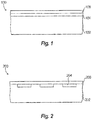
- Fig. 1 a partial view of an exemplary embodiment of a window for an imaging system in accordance with the disclosure is shown in Fig. 1 and is designated generally by reference character 100.
- the systems and methods described herein can be used to provide windows with electromagnetic interference (EMI) shielding for imaging systems.
- EMI electromagnetic interference
- Window 100 includes a transparent substrate 102 and a coating 104 over the transparent substrate 102.
- the coating 104 is made of an electrically conductive semiconductor, that is transparent to at least one of mid-wavelength infrared (MWIR) and/or long-wavelength infrared (LWIR) wavelengths.
- MWIR mid-wavelength infrared
- LWIR long-wavelength infrared
- the coating 104 has its peak transmission in MWIR wavelengths
- the transparent substrate 102 includes sapphire, aluminum oxynitride (AlON), and/or Spinel.
- the coatings can be doped with Te, S, Se, Si, or Sn to provide additional electrons for increased electrical conductivity.
- a suitable coating 104 for this peak transmission is InAs, a Te-doped InAs film (InAs:Te), which has low absorption in the 3 to 12 micron range with a peak transmission exceeding 80% from 4.6 to 5.1 microns without an anti-reflection (AR) coating.
- An optional anti-reflection coating 106 over the coating 104 increases transmittance through window 100.
- Other suitable coating materials for this application include InGaAs and/or InAlAs. These materials allow the coating 104 to have a sheet resistance of less than 200 ohms per square, with enough electron mobility to provide EMI shielding for imaging devices.
- the coating 104 can be is transparent in LWIR wavelengths, e.g., with its peak transmission in LWIR wavelengths.
- the transparent substrate 102 for such an application can include at least one of ZnS and/or ZnSe.
- Adding a group III element such as aluminum or gallium to InAs creates a compound (InGaAs, InAlAs) with a higher bandgap and extend transmission to shorter wavelengths.
- group III element such as aluminum or gallium
- InAs InGaAs, InAlAs
- such materials are expected to have lower electron mobility than InAs and reduced long wavelength transmission. Therefore, there is a compromise between SWIR and MWIR to LWIR transmission.
- the coating 104 is formed as a film on the transparent substrate 102. This can be accomplished by metalorganic chemical vapor deposition (MOCVD), evaporation, molecular beam epitaxy (MBE), chemical spray pyrolysis, chemical vapor deposition (CVD), aerosol-assisted CVD, and/or any other suitable process.
- MOCVD metalorganic chemical vapor deposition
- MBE molecular beam epitaxy
- CVD chemical vapor deposition
- aerosol-assisted CVD and/or any other suitable process.
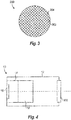
- a window 200 is shown with a transparent substrate 202.
- the coating 204 is embedded in a pattern in the transparent substrate 202.
- An anti-reflection coating 206 can optionally be included over the patterned surface of the substrate 202 and coating 206.
- the pattern can include a grid, or any other suitable pattern.
- the coating 204 and substrate 202 or base coating on the substrate can have closely matched indices of refraction to mitigate light scattering through the pattern.
- the pattern can extend transparency of the window 200 beyond the MWIR and LWIR wavelengths, e.g., into the visible wavelengths while still providing electrical conductivity for at least some EMI shielding.
- the pattern can be selected for a given application with a tradeoff between EMI shielding and transparency to wider bands balanced for the application.
- visible and SWIR wavelengths can transmit where there is no grid (between the grid lattices where substrate 202 is not covered with the grid of coating 204), and the grid itself can be transparent to MWIR and LWIR wavelengths.
- the optical system 10 includes a housing 12, an imaging device 14 housed within the housing, and a window 100 as described above in the housing 12 providing an optical path through the housing 12 to the imaging device 14 as indicated in Fig. 4 by the dashed line.
- the imaging device 14 includes optics 16 that are optically coupled with an imaging sensor 18 for forming images.
- the window 100 and housing provide EMI shielding to the components therein, including imaging device 14.
- the sensor 18 of the imaging device 14 is sensitive to and the coating is transparent to at least one of MWIR and/or LWIR wavelengths. If the sensor 18 is sensitive in only MWIR wavelengths (i.e.
- the window 100 need only be transparent in the MWIR wavelengths, e.g., using configurations as described above. If the sensor 18 is sensitive only to LWIR wavelengths, the window 100 need only be transparent in the LWIR wavelengths, e.g., using configurations as described above. If the sensor 18 is intended for imaging in the MWIR and LWIR, the window 100 can be configured as described above for transparency in both MWIR and LWIR wavelengths. While system 10 is described and shown using window 100 with a continuous film coating 104 as shown in Fig. 1 , window 200 of Figs. 2-3 can be used with the patterned coating 206 without departing from the scope of this disclosure.
Landscapes
- Chemical & Material Sciences (AREA)
- Physics & Mathematics (AREA)
- Engineering & Computer Science (AREA)
- Organic Chemistry (AREA)
- Materials Engineering (AREA)
- General Physics & Mathematics (AREA)
- Inorganic Chemistry (AREA)
- Optics & Photonics (AREA)
- Metallurgy (AREA)
- General Chemical & Material Sciences (AREA)
- Chemical Kinetics & Catalysis (AREA)
- Ceramic Engineering (AREA)
- Mechanical Engineering (AREA)
- Structural Engineering (AREA)
- Health & Medical Sciences (AREA)
- Toxicology (AREA)
- Thermal Sciences (AREA)
- Spectroscopy & Molecular Physics (AREA)
- Manufacturing & Machinery (AREA)
- Crystallography & Structural Chemistry (AREA)
- Geochemistry & Mineralogy (AREA)
- Life Sciences & Earth Sciences (AREA)
- Surface Treatment Of Optical Elements (AREA)
- Solid State Image Pick-Up Elements (AREA)
- Laminated Bodies (AREA)
- Shielding Devices Or Components To Electric Or Magnetic Fields (AREA)
- Light Receiving Elements (AREA)
- Microelectronics & Electronic Packaging (AREA)
- Transforming Light Signals Into Electric Signals (AREA)
- Chemical Vapour Deposition (AREA)
Abstract
Description
- The present disclosure relates to optical coatings, and more particularly to electrically conductive optical coatings.
- Electro-optic (EO) systems require windows to protect the sensor and electronics from outside elements. In addition to rain, dust, and the like, in many cases the window must also block electromagnetic interference (EMI) that would otherwise impede the EO system performance.
- EMI shielding can be accomplished with a window that is electrically conductive and optically transparent. There are three conventional types of shielding.
- The first type of EMI shielded window uses a semiconductor material such as silicon or germanium that is doped with a group V element such as phosphorous, arsenic, or antimony to supply additional electrons to provide electrical conductivity. These windows are opaque for visible wavelengths and are thus not useful for broadband EO systems.
- The second type of shielded window uses a continuous, transparent, conductive coating. These coatings consist of wide bandgap semiconductors such as indium oxide (In2O3) and zinc oxide (ZnO) that have broadband optical transparency. The semiconductors are doped to provide electrical conductivity. However, as doping increases to increase electrical conductivity and EMI attenuation, optical transmittance decreases. This effect begins at longer wavelengths where both plasma reflectance and free-carrier absorption from electrons decrease transmittance. Traditional transparent, conductive semiconductor coatings are practical only in the 0.4 to 2.0 micron range, short wavelength visible through short wavelength infrared (SWIR).
- The third type of shielded window is traditionally required for broadband applications from the visible to the long-wave infrared (LWIR). A grid of fine metal lines is applied on the surface of the window. Typical dimensions are 5-micron wide lines with 140 micron spacing. These gridded windows enable optical transmittance over a broad wavelength range, but they limit optical transmittance by obscuration and scattering.
-
U.S. Patent No. 9,276,034 - The conventional techniques have been considered satisfactory for their intended purpose. However, there is an ever present need for improved electrically conductive optical coatings, e.g., for MWIR and LWIR optics. This disclosure provides a solution for this problem.
- A window includes a transparent substrate and a coating over the transparent substrate. The coating is made of an electrically conductive semiconductor that is transparent to at least one of MWIR and/or LWIR wavelengths.
- The coating can have its peak transmission in MWIR wavelengths. The transparent substrate can include sapphire, aluminum oxynitride (AlON), and/or Spinel.
- The coating can be transparent in LWIR wavelengths. The transparent substrate can include at least one of ZnS and/or ZnSe.
- The coating can include InAs, InGaAs, and/or InAlAs. The coatings can be doped with Te, S, Se, Si, or Sn to provide additional electrons for increased electrical conductivity. The coating can be embedded in a pattern in the transparent substrate or in a base coating on the substrate. The pattern can include a grid. The coating and substrate or base coating can have closely matched indices of refraction to mitigate light scattering through the pattern. The coating can have a sheet resistance of less than 200 ohms per square. An anti-reflection coating can be included over the coating.
- An optical system includes a housing, an imaging device housed within the housing, and a window in the housing providing an optical path through the housing to the imaging device. The window includes a transparent substrate and a coating over the transparent substrate. The coating is made of an electrically conductive semiconductor. The imaging device is sensitive to and the coating is transparent to at least one of MWIR and/or LWIR wavelengths.
- A method of making a window for an optical system includes forming a coating on a transparent substrate. The coating can be formed as a film on the transparent substrate by at least one of metalorganic chemical vapor deposition (MOCVD), evaporation, molecular beam epitaxy (MBE), chemical spray pyrolysis, chemical vapor deposition (CVD), and/or aerosol-assisted CVD.
- These and other features of the systems and methods of the subject disclosure will become more readily apparent to those skilled in the art from the following detailed description of the preferred embodiments taken in conjunction with the drawings.
- So that those skilled in the art to which the subject disclosure appertains will readily understand how to make and use the devices and methods of the subject disclosure without undue experimentation, preferred embodiments thereof will be described in detail herein below with reference to certain figures, wherein:
-
Fig. 1 is a schematic side-elevation view of an exemplary embodiment of a window constructed in accordance with the present disclosure, showing the transparent substrate, the electrically conductive semiconductor coating, and an anti-reflection coating; -
Fig. 2 is a schematic side-elevation view of another exemplary embodiment of a window constructed in accordance with the present disclosure, showing the electrically conductive semiconductor coating embedded in a pattern in the transparent substrate; -
Fig. 3 is a schematic plan view of the window ofFig. 2 , showing the two-dimensional pattern; and -
Fig. 4 is a schematic view of an imaging system incorporating a window as shown inFig. 1 . - Reference will now be made to the drawings wherein like reference numerals identify similar structural features or aspects of the subject disclosure. For purposes of explanation and illustration, and not limitation, a partial view of an exemplary embodiment of a window for an imaging system in accordance with the disclosure is shown in
Fig. 1 and is designated generally byreference character 100. Other embodiments of windows in accordance with the disclosure, or aspects thereof, are provided inFigs. 2-4 , as will be described. The systems and methods described herein can be used to provide windows with electromagnetic interference (EMI) shielding for imaging systems. -
Window 100 includes atransparent substrate 102 and acoating 104 over thetransparent substrate 102. Thecoating 104 is made of an electrically conductive semiconductor, that is transparent to at least one of mid-wavelength infrared (MWIR) and/or long-wavelength infrared (LWIR) wavelengths. For example, in embodiments, thecoating 104 has its peak transmission in MWIR wavelengths, and thetransparent substrate 102 includes sapphire, aluminum oxynitride (AlON), and/or Spinel. The coatings can be doped with Te, S, Se, Si, or Sn to provide additional electrons for increased electrical conductivity. Asuitable coating 104 for this peak transmission is InAs, a Te-doped InAs film (InAs:Te), which has low absorption in the 3 to 12 micron range with a peak transmission exceeding 80% from 4.6 to 5.1 microns without an anti-reflection (AR) coating. An optionalanti-reflection coating 106 over thecoating 104 increases transmittance throughwindow 100. Other suitable coating materials for this application include InGaAs and/or InAlAs. These materials allow thecoating 104 to have a sheet resistance of less than 200 ohms per square, with enough electron mobility to provide EMI shielding for imaging devices. - It is also contemplated that the
coating 104 can be is transparent in LWIR wavelengths, e.g., with its peak transmission in LWIR wavelengths. Thetransparent substrate 102 for such an application can include at least one of ZnS and/or ZnSe. Adding a group III element such as aluminum or gallium to InAs creates a compound (InGaAs, InAlAs) with a higher bandgap and extend transmission to shorter wavelengths. However, such materials are expected to have lower electron mobility than InAs and reduced long wavelength transmission. Therefore, there is a compromise between SWIR and MWIR to LWIR transmission. - The
coating 104 is formed as a film on thetransparent substrate 102. This can be accomplished by metalorganic chemical vapor deposition (MOCVD), evaporation, molecular beam epitaxy (MBE), chemical spray pyrolysis, chemical vapor deposition (CVD), aerosol-assisted CVD, and/or any other suitable process. - Referring now to
Fig. 2 , another exemplary embodiment of awindow 200 is shown with atransparent substrate 202. Thecoating 204 is embedded in a pattern in thetransparent substrate 202. Ananti-reflection coating 206 can optionally be included over the patterned surface of thesubstrate 202 andcoating 206. As shown inFig. 3 , the pattern can include a grid, or any other suitable pattern. Thecoating 204 andsubstrate 202 or base coating on the substrate can have closely matched indices of refraction to mitigate light scattering through the pattern. The pattern can extend transparency of thewindow 200 beyond the MWIR and LWIR wavelengths, e.g., into the visible wavelengths while still providing electrical conductivity for at least some EMI shielding. - The pattern can be selected for a given application with a tradeoff between EMI shielding and transparency to wider bands balanced for the application. For example, visible and SWIR wavelengths can transmit where there is no grid (between the grid lattices where
substrate 202 is not covered with the grid of coating 204), and the grid itself can be transparent to MWIR and LWIR wavelengths. Furthermore, if the grid lines are embedded in a base coating or insubstrate 202 itself with a close index of refraction (n = 3.5 at 5 microns), diffraction from the grid is greatly reduced. There is a compromise between transmittance and sheet resistance as less surface area is covered by a grid than a continuous coating. - With reference now to
Fig. 4 , theoptical system 10 includes ahousing 12, animaging device 14 housed within the housing, and awindow 100 as described above in thehousing 12 providing an optical path through thehousing 12 to theimaging device 14 as indicated inFig. 4 by the dashed line. Theimaging device 14 includesoptics 16 that are optically coupled with animaging sensor 18 for forming images. Thewindow 100 and housing provide EMI shielding to the components therein, includingimaging device 14. Thesensor 18 of theimaging device 14 is sensitive to and the coating is transparent to at least one of MWIR and/or LWIR wavelengths. If thesensor 18 is sensitive in only MWIR wavelengths (i.e. has its peak sensitivity in MWIR wavelengths), thewindow 100 need only be transparent in the MWIR wavelengths, e.g., using configurations as described above. If thesensor 18 is sensitive only to LWIR wavelengths, thewindow 100 need only be transparent in the LWIR wavelengths, e.g., using configurations as described above. If thesensor 18 is intended for imaging in the MWIR and LWIR, thewindow 100 can be configured as described above for transparency in both MWIR and LWIR wavelengths. Whilesystem 10 is described and shown usingwindow 100 with acontinuous film coating 104 as shown inFig. 1 ,window 200 ofFigs. 2-3 can be used with the patternedcoating 206 without departing from the scope of this disclosure. - The methods and systems of the present disclosure, as described above and shown in the drawings, provide for electrically conductive coatings with superior properties including MWIR and/or LWIR optical transmittance. While the apparatus and methods of the subject disclosure have been shown and described with reference to preferred embodiments, those skilled in the art will readily appreciate that changes and/or modifications may be made thereto without departing from the scope of the subject disclosure.
Claims (15)
- A window (100) comprising:a transparent substrate (102); anda coating (104) over the transparent substrate (102), the coating (104) being made of an electrically conductive semiconductor, that is transparent to at least one of MWIR and/or LWIR wavelengths.
- The window as recited in claim 1, wherein the coating (104) has its peak transmission in MWIR wavelengths, and preferably wherein the transparent substrate includes sapphire, Aluminum Oxynitride (AlON), and/or Spinel.
- The window as recited in claim 1, wherein the coating (104) is transparent in LWIR wavelengths and preferably wherein the transparent substrate includes at least one of ZnS and/or ZnSe.
- The window as recited in claim 1, wherein the coating includes InAs or wherein the coating (104) is doped with at least one of Te, S, Se, Si, and/or Sn.
- The window as recited in claim 1, wherein the coating (104) includes InGaAs or wherein the coating (104) includes InAlAs.
- The window as recited in claim 1, wherein the coating (104) is formed as a film on the transparent substrate by at least one of metalorganic chemical vapor deposition (MOCVD), evaporation, molecular beam epitaxy (MBE), chemical spray pyrolysis, chemical vapor deposition (CVD), and/or aerosol-assisted CVD.
- The window as recited in claim 1, wherein the coating (104) is embedded in a pattern in the transparent substrate.
- The window as recited in claim 7, wherein the pattern includes a grid.
- The window as recited in claim 7, wherein the coating (104) and substrate have closely matched indices of refraction to mitigate light scattering through the pattern.
- The window as recited in claim 1, wherein the conductive coating (104) is embedded in a pattern in a transparent coating on the transparent substrate and preferably wherein the coating (104) and a transparent base coating have closely matched indices of refraction to mitigate light scattering through the pattern.
- The window as recited in any preceding claim, further comprising an anti-reflection coating over the coating (104).
- The window as recited in any preceding claim, wherein the coating (104) has a sheet resistance of less than 200 ohms per square.
- An optical system (10) comprising:a housing (12);an imaging device (14) housed within the housing (12) and the window (100) of any preceding claim,the window (100) in the housing (12) providing an optical path through the housing (12) to the imaging device (14),
wherein the imaging device (14) is sensitive to at least one of MWIR and/or LWIR wavelengths. - The system as recited in claim 13, wherein the coating (104) has its peak transmission in MWIR wavelengths, and wherein the imaging device (14) is sensitive to MWIR wavelengths or wherein the coating (104) is transparent in LWIR wavelengths, and wherein the imaging device (14) is sensitive to LWIR wavelengths.
- A method of making a window (100) for an optical system (10) comprising:
forming a coating (104) on a transparent substrate (102), wherein the coating (104) is an electrically conductive semiconductor film transparent to at least one of MWIR and/or LWIR wavelengths.
Applications Claiming Priority (1)
| Application Number | Priority Date | Filing Date | Title |
|---|---|---|---|
| US15/680,425 US10444409B2 (en) | 2017-08-18 | 2017-08-18 | MWIR/LWIR transparent, conductive coatings |
Publications (2)
| Publication Number | Publication Date |
|---|---|
| EP3453783A2 true EP3453783A2 (en) | 2019-03-13 |
| EP3453783A3 EP3453783A3 (en) | 2019-07-31 |
Family
ID=63294098
Family Applications (1)
| Application Number | Title | Priority Date | Filing Date |
|---|---|---|---|
| EP18189357.9A Pending EP3453783A3 (en) | 2017-08-18 | 2018-08-16 | Mwir/lwir transparent, conductive coatings |
Country Status (3)
| Country | Link |
|---|---|
| US (1) | US10444409B2 (en) |
| EP (1) | EP3453783A3 (en) |
| JP (1) | JP7226939B2 (en) |
Cited By (3)
| Publication number | Priority date | Publication date | Assignee | Title |
|---|---|---|---|---|
| WO2021042117A1 (en) * | 2019-08-23 | 2021-03-04 | Lam Research Corporation | Plasma viewport |
| GB2589665A (en) * | 2019-11-28 | 2021-06-09 | Rino Tech Dmcc | Lens |
| US12248122B2 (en) | 2021-02-01 | 2025-03-11 | Raytheon Company | SWIR-MWIR transparent, conductive coating for EMI protection of NCOC |
Families Citing this family (2)
| Publication number | Priority date | Publication date | Assignee | Title |
|---|---|---|---|---|
| KR102758729B1 (en) | 2019-07-24 | 2025-01-22 | 삼성전자주식회사 | Substrate treating apparatus and substrate treating system having the same |
| JP2021162728A (en) * | 2020-03-31 | 2021-10-11 | デクセリアルズ株式会社 | Optical body, method of manufacturing optical body, and optical device |
Citations (1)
| Publication number | Priority date | Publication date | Assignee | Title |
|---|---|---|---|---|
| US9276034B2 (en) | 2014-04-07 | 2016-03-01 | Goodrich Corporation | Grid topography for patterned semiconductor coating that minimizes optical scatter and obscuration |
Family Cites Families (13)
| Publication number | Priority date | Publication date | Assignee | Title |
|---|---|---|---|---|
| US2977477A (en) | 1958-05-28 | 1961-03-28 | Rca Corp | Semiconductive materials for infrared transmissive components |
| US5012112A (en) | 1989-02-21 | 1991-04-30 | Martin Marietta Corporation | Infrared scene projector |
| JPH07120319A (en) * | 1993-10-22 | 1995-05-12 | Sumitomo Electric Ind Ltd | Infrared transmitting structure with radio wave shielding property |
| ES2186706T3 (en) * | 1994-10-13 | 2003-05-16 | Raytheon Co | TRANSPARENT WINDOW TRANSPARENT TO INFRARED LENGTH OF LONG WAVES. |
| US6181468B1 (en) | 1994-11-16 | 2001-01-30 | Raytheon Company | Composite infrared windows fabricated by direct bonding |
| US6761986B2 (en) * | 2001-04-06 | 2004-07-13 | Rockwell Scientific Licensing, Llc | Thin film infrared transparent conductor |
| JP3894107B2 (en) * | 2002-11-28 | 2007-03-14 | 三菱電機株式会社 | Infrared antireflection film |
| US7180064B2 (en) | 2003-07-24 | 2007-02-20 | Delphi Technologies, Inc. | Infrared sensor package |
| US7601946B2 (en) * | 2006-09-12 | 2009-10-13 | Ravenbrick, Llc | Electromagnetic sensor incorporating quantum confinement structures |
| US7936500B2 (en) * | 2007-03-02 | 2011-05-03 | Ravenbrick Llc | Wavelength-specific optical switch |
| US9007520B2 (en) * | 2012-08-10 | 2015-04-14 | Nanchang O-Film Optoelectronics Technology Ltd | Camera module with EMI shield |
| WO2015199624A1 (en) * | 2014-06-23 | 2015-12-30 | Aselsan Elektronik Sanayi Ve Ticaret Anonim Şirketi | A graphene based emi shielding optical coating |
| US10000642B2 (en) * | 2014-09-05 | 2018-06-19 | Raytheon Company | Long wave infrared transparent window and coating materials |
-
2017
- 2017-08-18 US US15/680,425 patent/US10444409B2/en active Active
-
2018
- 2018-08-16 EP EP18189357.9A patent/EP3453783A3/en active Pending
- 2018-08-17 JP JP2018153348A patent/JP7226939B2/en active Active
Patent Citations (1)
| Publication number | Priority date | Publication date | Assignee | Title |
|---|---|---|---|---|
| US9276034B2 (en) | 2014-04-07 | 2016-03-01 | Goodrich Corporation | Grid topography for patterned semiconductor coating that minimizes optical scatter and obscuration |
Cited By (5)
| Publication number | Priority date | Publication date | Assignee | Title |
|---|---|---|---|---|
| WO2021042117A1 (en) * | 2019-08-23 | 2021-03-04 | Lam Research Corporation | Plasma viewport |
| US12272534B2 (en) | 2019-08-23 | 2025-04-08 | Lam Researh Corporation | Plasma viewport |
| GB2589665A (en) * | 2019-11-28 | 2021-06-09 | Rino Tech Dmcc | Lens |
| GB2589665B (en) * | 2019-11-28 | 2022-02-16 | Cenegex Ltd | Window Assembly |
| US12248122B2 (en) | 2021-02-01 | 2025-03-11 | Raytheon Company | SWIR-MWIR transparent, conductive coating for EMI protection of NCOC |
Also Published As
| Publication number | Publication date |
|---|---|
| EP3453783A3 (en) | 2019-07-31 |
| US10444409B2 (en) | 2019-10-15 |
| US20190056532A1 (en) | 2019-02-21 |
| JP2019036732A (en) | 2019-03-07 |
| JP7226939B2 (en) | 2023-02-21 |
Similar Documents
| Publication | Publication Date | Title |
|---|---|---|
| US10444409B2 (en) | MWIR/LWIR transparent, conductive coatings | |
| US12399430B2 (en) | Apparatus and methods of electrically conductive optical semiconductor coating | |
| WO2015199624A1 (en) | A graphene based emi shielding optical coating | |
| JP7593978B2 (en) | Apparatus and method for conductive photo-semiconductor coatings | |
| KR102615200B1 (en) | A stealth element constituted by multiple thin layers on MXene substrate for visible and infrared camouflage | |
| JP2026012563A (en) | Optical substrate coating method and window | |
| US9276034B2 (en) | Grid topography for patterned semiconductor coating that minimizes optical scatter and obscuration | |
| US5724180A (en) | Long wavelength infrared transparent conductive window | |
| JP6842327B2 (en) | Radiation detector and radiation detector |
Legal Events
| Date | Code | Title | Description |
|---|---|---|---|
| PUAI | Public reference made under article 153(3) epc to a published international application that has entered the european phase |
Free format text: ORIGINAL CODE: 0009012 |
|
| STAA | Information on the status of an ep patent application or granted ep patent |
Free format text: STATUS: THE APPLICATION HAS BEEN PUBLISHED |
|
| AK | Designated contracting states |
Kind code of ref document: A2 Designated state(s): AL AT BE BG CH CY CZ DE DK EE ES FI FR GB GR HR HU IE IS IT LI LT LU LV MC MK MT NL NO PL PT RO RS SE SI SK SM TR |
|
| AX | Request for extension of the european patent |
Extension state: BA ME |
|
| PUAL | Search report despatched |
Free format text: ORIGINAL CODE: 0009013 |
|
| AK | Designated contracting states |
Kind code of ref document: A3 Designated state(s): AL AT BE BG CH CY CZ DE DK EE ES FI FR GB GR HR HU IE IS IT LI LT LU LV MC MK MT NL NO PL PT RO RS SE SI SK SM TR |
|
| AX | Request for extension of the european patent |
Extension state: BA ME |
|
| RIC1 | Information provided on ipc code assigned before grant |
Ipc: G02B 5/20 20060101ALI20190625BHEP Ipc: C23C 16/30 20060101AFI20190625BHEP Ipc: C30B 29/40 20060101ALI20190625BHEP Ipc: G01J 5/08 20060101ALI20190625BHEP Ipc: G02B 1/113 20150101ALI20190625BHEP Ipc: C23C 18/12 20060101ALI20190625BHEP Ipc: G02B 1/118 20150101ALI20190625BHEP Ipc: G02B 13/14 20060101ALI20190625BHEP Ipc: G02B 1/16 20150101ALI20190625BHEP Ipc: G01J 5/06 20060101ALN20190625BHEP |
|
| STAA | Information on the status of an ep patent application or granted ep patent |
Free format text: STATUS: REQUEST FOR EXAMINATION WAS MADE |
|
| 17P | Request for examination filed |
Effective date: 20191118 |
|
| RBV | Designated contracting states (corrected) |
Designated state(s): AL AT BE BG CH CY CZ DE DK EE ES FI FR GB GR HR HU IE IS IT LI LT LU LV MC MK MT NL NO PL PT RO RS SE SI SK SM TR |
|
| STAA | Information on the status of an ep patent application or granted ep patent |
Free format text: STATUS: EXAMINATION IS IN PROGRESS |
|
| 17Q | First examination report despatched |
Effective date: 20210920 |