EP3451531A1 - Method for improving feedback circuit performance - Google Patents
Method for improving feedback circuit performance Download PDFInfo
- Publication number
- EP3451531A1 EP3451531A1 EP17188158.4A EP17188158A EP3451531A1 EP 3451531 A1 EP3451531 A1 EP 3451531A1 EP 17188158 A EP17188158 A EP 17188158A EP 3451531 A1 EP3451531 A1 EP 3451531A1
- Authority
- EP
- European Patent Office
- Prior art keywords
- amplifier
- amplitude values
- improving performance
- feedback circuit
- analog
- Prior art date
- Legal status (The legal status is an assumption and is not a legal conclusion. Google has not performed a legal analysis and makes no representation as to the accuracy of the status listed.)
- Granted
Links
Images


Classifications
-
- H—ELECTRICITY
- H03—ELECTRONIC CIRCUITRY
- H03M—CODING; DECODING; CODE CONVERSION IN GENERAL
- H03M1/00—Analogue/digital conversion; Digital/analogue conversion
- H03M1/12—Analogue/digital converters
- H03M1/18—Automatic control for modifying the range of signals the converter can handle, e.g. gain ranging
- H03M1/181—Automatic control for modifying the range of signals the converter can handle, e.g. gain ranging in feedback mode, i.e. by determining the range to be selected from one or more previous digital output values
- H03M1/183—Automatic control for modifying the range of signals the converter can handle, e.g. gain ranging in feedback mode, i.e. by determining the range to be selected from one or more previous digital output values the feedback signal controlling the gain of an amplifier or attenuator preceding the analogue/digital converter
-
- G—PHYSICS
- G01—MEASURING; TESTING
- G01R—MEASURING ELECTRIC VARIABLES; MEASURING MAGNETIC VARIABLES
- G01R29/00—Arrangements for measuring or indicating electric quantities not covered by groups G01R19/00 - G01R27/00
- G01R29/26—Measuring noise figure; Measuring signal-to-noise ratio
-
- G—PHYSICS
- G05—CONTROLLING; REGULATING
- G05F—SYSTEMS FOR REGULATING ELECTRIC OR MAGNETIC VARIABLES
- G05F1/00—Automatic systems in which deviations of an electric quantity from one or more predetermined values are detected at the output of the system and fed back to a device within the system to restore the detected quantity to its predetermined value or values, i.e. retroactive systems
- G05F1/70—Regulating power factor; Regulating reactive current or power
-
- H—ELECTRICITY
- H03—ELECTRONIC CIRCUITRY
- H03F—AMPLIFIERS
- H03F1/00—Details of amplifiers with only discharge tubes, only semiconductor devices or only unspecified devices as amplifying elements
- H03F1/30—Modifications of amplifiers to reduce influence of variations of temperature or supply voltage or other physical parameters
- H03F1/301—Modifications of amplifiers to reduce influence of variations of temperature or supply voltage or other physical parameters in MOSFET amplifiers
-
- H—ELECTRICITY
- H03—ELECTRONIC CIRCUITRY
- H03F—AMPLIFIERS
- H03F1/00—Details of amplifiers with only discharge tubes, only semiconductor devices or only unspecified devices as amplifying elements
- H03F1/30—Modifications of amplifiers to reduce influence of variations of temperature or supply voltage or other physical parameters
- H03F1/307—Modifications of amplifiers to reduce influence of variations of temperature or supply voltage or other physical parameters in push-pull amplifiers
- H03F1/308—Modifications of amplifiers to reduce influence of variations of temperature or supply voltage or other physical parameters in push-pull amplifiers using MOSFET
-
- H—ELECTRICITY
- H03—ELECTRONIC CIRCUITRY
- H03F—AMPLIFIERS
- H03F1/00—Details of amplifiers with only discharge tubes, only semiconductor devices or only unspecified devices as amplifying elements
- H03F1/32—Modifications of amplifiers to reduce non-linear distortion
- H03F1/3205—Modifications of amplifiers to reduce non-linear distortion in field-effect transistor amplifiers
-
- H—ELECTRICITY
- H03—ELECTRONIC CIRCUITRY
- H03F—AMPLIFIERS
- H03F1/00—Details of amplifiers with only discharge tubes, only semiconductor devices or only unspecified devices as amplifying elements
- H03F1/32—Modifications of amplifiers to reduce non-linear distortion
- H03F1/3211—Modifications of amplifiers to reduce non-linear distortion in differential amplifiers
-
- H—ELECTRICITY
- H03—ELECTRONIC CIRCUITRY
- H03F—AMPLIFIERS
- H03F1/00—Details of amplifiers with only discharge tubes, only semiconductor devices or only unspecified devices as amplifying elements
- H03F1/32—Modifications of amplifiers to reduce non-linear distortion
- H03F1/3217—Modifications of amplifiers to reduce non-linear distortion in single ended push-pull amplifiers
-
- H—ELECTRICITY
- H03—ELECTRONIC CIRCUITRY
- H03F—AMPLIFIERS
- H03F1/00—Details of amplifiers with only discharge tubes, only semiconductor devices or only unspecified devices as amplifying elements
- H03F1/34—Negative-feedback-circuit arrangements with or without positive feedback
- H03F1/342—Negative-feedback-circuit arrangements with or without positive feedback in field-effect transistor amplifiers
-
- H—ELECTRICITY
- H03—ELECTRONIC CIRCUITRY
- H03F—AMPLIFIERS
- H03F3/00—Amplifiers with only discharge tubes or only semiconductor devices as amplifying elements
- H03F3/005—Amplifiers with only discharge tubes or only semiconductor devices as amplifying elements using switched capacitors, e.g. dynamic amplifiers; using switched capacitors as resistors in differential amplifiers
-
- H—ELECTRICITY
- H03—ELECTRONIC CIRCUITRY
- H03F—AMPLIFIERS
- H03F3/00—Amplifiers with only discharge tubes or only semiconductor devices as amplifying elements
- H03F3/30—Single-ended push-pull [SEPP] amplifiers; Phase-splitters therefor
- H03F3/3001—Single-ended push-pull [SEPP] amplifiers; Phase-splitters therefor with field-effect transistors
- H03F3/3022—CMOS common source output SEPP amplifiers
- H03F3/3028—CMOS common source output SEPP amplifiers with symmetrical driving of the end stage
-
- H—ELECTRICITY
- H03—ELECTRONIC CIRCUITRY
- H03F—AMPLIFIERS
- H03F3/00—Amplifiers with only discharge tubes or only semiconductor devices as amplifying elements
- H03F3/45—Differential amplifiers
- H03F3/45071—Differential amplifiers with semiconductor devices only
- H03F3/45076—Differential amplifiers with semiconductor devices only characterised by the way of implementation of the active amplifying circuit in the differential amplifier
- H03F3/45179—Differential amplifiers with semiconductor devices only characterised by the way of implementation of the active amplifying circuit in the differential amplifier using MOSFET transistors as the active amplifying circuit
- H03F3/45183—Long tailed pairs
-
- H—ELECTRICITY
- H03—ELECTRONIC CIRCUITRY
- H03F—AMPLIFIERS
- H03F3/00—Amplifiers with only discharge tubes or only semiconductor devices as amplifying elements
- H03F3/45—Differential amplifiers
- H03F3/45071—Differential amplifiers with semiconductor devices only
- H03F3/45076—Differential amplifiers with semiconductor devices only characterised by the way of implementation of the active amplifying circuit in the differential amplifier
- H03F3/45179—Differential amplifiers with semiconductor devices only characterised by the way of implementation of the active amplifying circuit in the differential amplifier using MOSFET transistors as the active amplifying circuit
- H03F3/45237—Complementary long tailed pairs having parallel inputs and being supplied in series
-
- H—ELECTRICITY
- H03—ELECTRONIC CIRCUITRY
- H03F—AMPLIFIERS
- H03F3/00—Amplifiers with only discharge tubes or only semiconductor devices as amplifying elements
- H03F3/45—Differential amplifiers
- H03F3/45071—Differential amplifiers with semiconductor devices only
- H03F3/45076—Differential amplifiers with semiconductor devices only characterised by the way of implementation of the active amplifying circuit in the differential amplifier
- H03F3/45475—Differential amplifiers with semiconductor devices only characterised by the way of implementation of the active amplifying circuit in the differential amplifier using IC blocks as the active amplifying circuit
-
- H—ELECTRICITY
- H03—ELECTRONIC CIRCUITRY
- H03F—AMPLIFIERS
- H03F3/00—Amplifiers with only discharge tubes or only semiconductor devices as amplifying elements
- H03F3/50—Amplifiers in which input is applied to, or output is derived from, an impedance common to input and output circuits of the amplifying element, e.g. cathode follower
- H03F3/505—Amplifiers in which input is applied to, or output is derived from, an impedance common to input and output circuits of the amplifying element, e.g. cathode follower with field-effect devices
-
- H—ELECTRICITY
- H03—ELECTRONIC CIRCUITRY
- H03M—CODING; DECODING; CODE CONVERSION IN GENERAL
- H03M13/00—Coding, decoding or code conversion, for error detection or error correction; Coding theory basic assumptions; Coding bounds; Error probability evaluation methods; Channel models; Simulation or testing of codes
- H03M13/61—Aspects and characteristics of methods and arrangements for error correction or error detection, not provided for otherwise
- H03M13/612—Aspects specific to channel or signal-to-noise ratio estimation
-
- H—ELECTRICITY
- H03—ELECTRONIC CIRCUITRY
- H03F—AMPLIFIERS
- H03F2200/00—Indexing scheme relating to amplifiers
- H03F2200/129—Indexing scheme relating to amplifiers there being a feedback over the complete amplifier
-
- H—ELECTRICITY
- H03—ELECTRONIC CIRCUITRY
- H03F—AMPLIFIERS
- H03F2200/00—Indexing scheme relating to amplifiers
- H03F2200/135—Indexing scheme relating to amplifiers there being a feedback over one or more internal stages in the global amplifier
-
- H—ELECTRICITY
- H03—ELECTRONIC CIRCUITRY
- H03F—AMPLIFIERS
- H03F2200/00—Indexing scheme relating to amplifiers
- H03F2200/153—Feedback used to stabilise the amplifier
-
- H—ELECTRICITY
- H03—ELECTRONIC CIRCUITRY
- H03F—AMPLIFIERS
- H03F2200/00—Indexing scheme relating to amplifiers
- H03F2200/156—One or more switches are realised in the feedback circuit of the amplifier stage
-
- H—ELECTRICITY
- H03—ELECTRONIC CIRCUITRY
- H03F—AMPLIFIERS
- H03F2200/00—Indexing scheme relating to amplifiers
- H03F2200/159—Indexing scheme relating to amplifiers the feedback circuit being closed during a switching time
-
- H—ELECTRICITY
- H03—ELECTRONIC CIRCUITRY
- H03F—AMPLIFIERS
- H03F2200/00—Indexing scheme relating to amplifiers
- H03F2200/249—A switch coupled in the input circuit of an amplifier being controlled by a circuit, e.g. feedback circuitry being controlling the switch
-
- H—ELECTRICITY
- H03—ELECTRONIC CIRCUITRY
- H03F—AMPLIFIERS
- H03F2200/00—Indexing scheme relating to amplifiers
- H03F2200/252—Multiple switches coupled in the input circuit of an amplifier are controlled by a circuit, e.g. feedback circuitry being controlling the switch
-
- H—ELECTRICITY
- H03—ELECTRONIC CIRCUITRY
- H03F—AMPLIFIERS
- H03F2200/00—Indexing scheme relating to amplifiers
- H03F2200/27—A biasing circuit node being switched in an amplifier circuit
-
- H—ELECTRICITY
- H03—ELECTRONIC CIRCUITRY
- H03F—AMPLIFIERS
- H03F2200/00—Indexing scheme relating to amplifiers
- H03F2200/42—Indexing scheme relating to amplifiers the input to the amplifier being made by capacitive coupling means
-
- H—ELECTRICITY
- H03—ELECTRONIC CIRCUITRY
- H03F—AMPLIFIERS
- H03F2200/00—Indexing scheme relating to amplifiers
- H03F2200/471—Indexing scheme relating to amplifiers the voltage being sensed
-
- H—ELECTRICITY
- H03—ELECTRONIC CIRCUITRY
- H03F—AMPLIFIERS
- H03F2200/00—Indexing scheme relating to amplifiers
- H03F2200/546—A tunable capacitance being present in an amplifier circuit
-
- H—ELECTRICITY
- H03—ELECTRONIC CIRCUITRY
- H03F—AMPLIFIERS
- H03F2200/00—Indexing scheme relating to amplifiers
- H03F2200/78—A comparator being used in a controlling circuit of an amplifier
Definitions
- the present invention is generally related to the field of techniques for improving the performance of a feedback circuit comprising an amplifier.
- the performance of feedback circuits comprising an amplifier is typically quantified by its stability, noise performance and overall optimality.
- the stability is affected by various factors among which the process, voltage and temperature (PVT) variations, distortion and noise are most prominent.
- PVT voltage and temperature
- ring amplification - an amplification paradigm commonly used in switched capacitor feedback circuits - offers several prominent advantages in scaled CMOS technologies.
- the stability of ring amplifiers (ringamps) must be carefully considered.
- the invention in a first aspect relates to a method for improving performance of a feedback circuit comprising an amplifier and a feedback network, said feedback circuit having at least one tuneable component.
- the method comprises
- the proposed solution allows for obtaining an estimate of the the signal-to-noise-plus-distortion ratio, which can subsequently be used for tuning the feedback circuit.
- estimating the linear open-loop gain comprises an averaging of the first and the second plurality of amplitude values.
- a binning technique is applied to speed up said averaging.
- a first analog-to-digital converter is used for measuring the first plurality of amplitude values and a second analog-to-digital converter for the second plurality of amplitude values at the amplifier output, said first and said second analog-to-digital converter arranged for sampling synchronously.
- the first analog-to-digital converter is preferably a stochastic ADC comprising a noisy comparator.
- the signal-to-noise-plus-distortion ratio estimate is replaced by a total harmonic distortion estimate.
- the method comprises a step of removing static offset from the set of processed samples.
- the amplifier is a ring amplifier.
- said ring amplifier is part of a pipelined analog-to-digital converter with a plurality of stages, each stage having a multiplying digital-to-analog converter, MDAC, feedback circuit.
- the method then preferably comprises a step of monitoring the ring amplifier while the pipelined ADC is operative.
- the performance is improved by tuning the stability of the feedback circuit.
- the present invention proposes a technique for improving the overall performance of a feedback circuit comprising an amplifier by using a signal-to-noise-plus-distortion ratio (SNDR) as an indication of presence of uncorrected errors.
- SNDR signal-to-noise-plus-distortion ratio
- the quantified information on errors can then be used as such or in a calibration algorithm to optimize the circuit performance in terms of SNDR by adjusting the circuit's tuneable components.
- the essence of the present invention lies in a novel technique for determining the SNDR of feedback circuits and using this measure for improving the circuit's performance.
- the proposed technique can be applied in numerous applications. For example, it can be used for improving the stability of a feedback circuit which affects the circuit performance, as stability is reflected in the SNDR measure of the circuit. Similarly, it can be used for optimizing the ringamp settling behaviour in switched capacitor circuits such as pipelined ADCs.
- Another example application is the cancellation of non-linear distortion in an amplifier. Non-linear distortion is observed in an amplifier (e.g. operational amplifier, ring amplifier or any other amplifier) that has a dominant 3 rd harmonic. In such case, the 3 rd harmonic dominates the SNDR of the circuit.
- the tuneable element is adjusted until the SNDR is maximized, indicating that the distortion is minimized.
- the method extends its usefulness to many types of amplifier and feedback structures.
- the approach is applicable to any type of operational amplifier and any type of resistive or switched-capacitor feedback network.
- Amplifier-wise this includes the broad class of transconductance amplifiers, but also extends to other types such as ringamps.
- Application-wise this includes circuits where feedback networks are used such as filters, ADCs, sensors, buffers and signal processing in general.
- the invention is, however, first explained in its broader context. A method will be presented for approximating the circuit's SNDR. The invention will then be explained in the context of a ringamp in an MDAC feedback circuit in a pipeline ADC as a background stability tracking and tuning scheme.
- a general feedback circuit containing an amplifier with a finite gain A OL , having input node V X and output node V OUT and a feedback network ( ⁇ ) as illustrated in FIG.1 is considered.
- the voltages at nodes V X and V OUT are measured.
- Connected to nodes V X and V OUT are ADCs that sample and digitize the voltage values at these nodes.
- the output of each ADC is a stream of digitized sampled voltage values.
- the proposed method determines both the linear open-loop gain of the amplifier (A OL ) and the SNDR of the circuit as detailed below.
- V X The signal present at V X is composed of several error sources such as: linear finite gain error, non-linear finite gain error, incomplete settling error and random noise sources.
- V X there is no component in V X that is part of the wanted signal, i.e. V X is only error.
- V OUT by comparison, is primarily composed of the actual wanted signal; noise and distortion are still present, but at much lower relative levels.
- V X and V OUT nodes are periodically sampled and digitized by ADC1 and ADC2, respectively.
- two streams of digitized V OUT and V X values i.e. D(V OUT ) and D(V X ) are obtained, which correspond to two vectors of data acquired from the output of ADC1 and ADC2.
- the quantized values for V OUT and V X are obtained.
- These two vectors are aligned, i.e. the voltage values at the input and at the output of the amplifier are sampled at the same time instant.
- an estimate of the linear open-loop gain of the amplifier ( ⁇ OL ) can be calculated from a large number of samples of V X and V OUT as:
- a ⁇ OL ⁇ V out , i , q 2 ⁇ V out , i , q V x , i , q , where i is the sample number, V out,i,q is the quantized value of V OUT as generated by ADC2 and V x,i,q is the quantized value of V X as generated by ADC1.
- q is used to denote V x and V out is quantized.
- ADC1 can be replaced by a stochastic ADC comprising a noisy comparator.
- a ⁇ OL ⁇ V out , i , q 2 ⁇ V out , i , q V ⁇ x , i , where V ⁇ x,i is the estimation of V X for sample i. Note that all samples with the same digitized V OUT value will use the same estimation for V X . To get a good estimation of V X , many samples are needed, typically in the order of a few thousand. When there are 2 N different digitized V OUT values, there are also 2 N different V X estimates and the total number of points needed to compute all V X estimates and subsequently the open-loop gain estimate quickly ranges from a few hundred thousand to a few million. The number of samples needed depends on the accuracy of the required estimate and on the resolution of ADC1 and ADC2.
- a so-called binning technique is introduced.
- the binning significantly reduces the number of samples to be used to obtain a ⁇ OL value of a sufficiently high accuracy.
- continuous ranges of V OUT codes can be grouped together and their V X values can be placed into so-called bins to speed up processing. All values in a bin are used to compute the estimation of V X .
- the estimations V ⁇ x,i used in the computation of ⁇ OL only take as many different values as the number of bins. Numerous approaches to an exact implementation of binning are possible.
- V OUT can validly be assumed a sufficiently accurate approximation of the ideal output signal, the component of V X due to linear finite gain error can be removed since it is simply a scaled replica of V OUT .
- Vx V OUT A ⁇ OL
- Vx Equation (4) yields a vector of processed samples containing only the information about nonlinearities, settling error and random noise processes in the feedback circuit. In case these error sources are not zero-mean, an extra processing step may be needed to remove the static offset.
- the average uncalibrated error power present at V X node can be expressed as a scalar: var ⁇ other , Vx
- the computed value is not an exact SNDR value, since V OUT is assumed to be noiseless whereas in fact it also contains noise that is erroneously treated as signal here. However, for practical uses this does not pose a problem since it is typically not needed to know the exact SNDR value, only the relative change in SNDR with respect to some optimization control variable is of interest.
- THD estimate var sign Vx ⁇ mean V OUT A OL ⁇ V OUT A OL var V OUT
- THD estimate var sign Vx ⁇ mean V OUT A OL ⁇ V OUT A OL var V OUT
- THD Total Harmonic Distortion
- the SNDR value is fed to a control unit which aims at maximizing the SNDR by adjusting the circuit's tuneable components.
- the SNDR value may be used as such.
- the control unit will adjust the tuneable components (increase or decrease) until the maximum SNDR value is reached.
- the SNDR value can be used in an algorithm, such as least mean squares (LMS) or gradient descent so that a faster convergence to a maximum SNDR value is reached.
- LMS least mean squares
- the tuning can be achieved in various ways known to skilled person. For example, for a two-stage Miller compensated operational transconductance amplifier (OTA) illustrated in FIG.2 , the SNDR gives an indication of the circuit's stability. By tracking the SNDR and tuning, for example, by digitally adjusting the size of the Miller capacitor C M connected between the opamp's stage 1 output and stage 2 output, and/or by changing the bias currents of stage 1 or stage 2 of the transistors indicated as variable elements, the stability can be maintained.
- OTA Miller compensated operational transconductance amplifier
- Ring amplifiers may be implemented in many different ways, each having their own possibilities for tuning. A full generalization of the possible ringamp tuning techniques is therefore difficult to give. However, some specific examples are presented here.
- the stability can be adjusted by varying the dead-zone voltage V DZ used to program the voltage offset on the capacitors at the output of stage 1.
- V DZ dead-zone voltage
- variable voltages at DZN and DZP nodes can be used to adjust the dynamic biasing resistance and thus the ringamp's stability performance.
- the invention will now be described in the context of a pipelined ADC MDAC as shown in FIG.5 and using a ring amplifier as in FIG.3 .
- the linear finite gain error and the ringamp settling/stability of the ring amplifier are PVT dependent. Hence, to improve the circuit's performance these parameters need to be tracked and corrected continuously. This correction is in a preferred embodiment performed in the background.
- the proposed method can be applied here to improve the linear finite gain error and ringamp settling/stability using the proposed method. Recall that the method relies on knowledge of V OUT (here, this is the output of the given pipeline stage's residue) and V X (the "virtual ground” floating node at the amplifier input in FIG.1 ).
- V OUT a digital version is already available in a pipelined ADC, since is simply the reconstructed digital output of all subsequent stages. This makes the proposed technique particularly well suited for use in pipelined ADCs.
- V X additional hardware is needed to obtain D(V X ), which may be a high or low resolution ADC, or be as simple as a noisy comparator as shown in FIG.6 .
- FIG.7 showing a block scheme of the proposed method. For each value of V OUT digitized with high precision by ADC2, a related quantization of V X is taken. This quantization of V X can be lower than the required resolution, even as low as 1 bit resolution. A so-called binning technique is used next.
- the bin width 1, for the 2-dimensional vector of output sets ⁇ D(V OUT ), D(V X ) ⁇ , the values of all D(V X ) corresponding to a unique value are averaged together. This is done for all values of D(V OUT ). The result is a bin for each unique value of D(V OUT ), said bin being the average value of D(V X ) associated with that value of D(V OUT ). Then, the average D(V X ) value in each bin is passed through an inverse error function (erfinv) and scaled with respect to the V REF of the stochastic ADC (obtained by quantizing a known reference voltage with the stochastic ADC).
- erfinv inverse error function
- a bin width larger than 1 can be used, wherein a continuous range of values is associated with each bin. If bins containing a uniform distribution of V OUT are available, simple averaging of the V X values regardless of the bin width is sufficient. However, if the distribution is non-uniform, as is the case with many modulated signals, simple averaging of the V X values in the bin increases the quantization error for bin widths > 1. It is possible to reduce this error by tracking the distribution of V OUT values in the input vector associated with that bin that occur, and then weight the V X values in the bin based on the knowledge of this distribution and according to their associated V OUT value, prior to averaging the V X values.
- the calculated SNDR can then be used as a performance indicator according to which the ring amplifier can be tuned.
- the SNDR parameter is then fed to a control block (not shown in FIG.7 ) which using the SNDR value as such or in an algorithm such as an LMS or gradient descent technique, outputs a control signal that controls the tuneable components of the circuit (i.e. V DZ of the ringamp). Due to the use of the ⁇ OL and specific formulation of the Equations (8) and (9), a faster convergence and resilience to numerical noise is obtained.
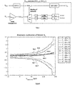
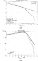
- FIG.8 illustrates Matlab simulation results for the method implementation of FIG.7.
- FIG.8A shows for a select subset of 8 bins the estimated (solid lines) and ideal averaged values (dashed lines) of V X versus the ringamp's stability tuning parameter V DZ .
- a binning segmentation of eight bins evenly divided across the full range of V OUT values is used. Due to binning, even with a relatively low total number of samples (e.g. 10k), a sufficiently accurate estimation of V X can be obtained for eight discrete bins when using the noisy comparator to measure V X .
- FIG.8B shows the estimated (labelled 'Estimation') and ideal values (labelled 'AC result') of the open-loop gain A OL versus the tuning parameter V DZ when the estimator implements Equations (8) and (9).
- V OUT the subsequent stages of the pipelined ADC are used.
- the estimation of the SNDR is shown in FIG. 8C which compares the estimation with the ideal value obtained via FFT computations.
- a computer program may be stored/distributed on a suitable medium, such as an optical storage medium or a solid-state medium supplied together with or as part of other hardware, but may also be distributed in other forms, such as via the Internet or other wired or wireless telecommunication systems. Any reference signs in the claims should not be construed as limiting the scope.
Landscapes
- Engineering & Computer Science (AREA)
- Power Engineering (AREA)
- Physics & Mathematics (AREA)
- Nonlinear Science (AREA)
- General Physics & Mathematics (AREA)
- Theoretical Computer Science (AREA)
- Electromagnetism (AREA)
- Radar, Positioning & Navigation (AREA)
- Automation & Control Theory (AREA)
- Probability & Statistics with Applications (AREA)
- Amplifiers (AREA)
Description
- The present invention is generally related to the field of techniques for improving the performance of a feedback circuit comprising an amplifier.
- The performance of feedback circuits comprising an amplifier is typically quantified by its stability, noise performance and overall optimality. The stability is affected by various factors among which the process, voltage and temperature (PVT) variations, distortion and noise are most prominent. However, in practical implementations it is not always possible to guarantee optimal stability of feedback circuits if employing a non-tuneable amplifier circuit across all PVT variation corners. In such a case, it is necessary to have a background calibration to maintain optimal performance conditions. For example, ring amplification - an amplification paradigm commonly used in switched capacitor feedback circuits - offers several prominent advantages in scaled CMOS technologies. However, due to their dynamic mechanisms of self-stabilization, the stability of ring amplifiers (ringamps) must be carefully considered.
- Hence, there is a need for techniques to maintain optimal performance in case a feedback circuit is present in such schemes.
- It is an object of embodiments of the present invention to provide for a method to improve the performance of a feedback circuit as used in various types of feedback structures.
- The above objective is accomplished by the solution according to the present invention.
- In a first aspect the invention relates to a method for improving performance of a feedback circuit comprising an amplifier and a feedback network, said feedback circuit having at least one tuneable component. The method comprises
- measuring a first plurality of amplitude values at an input of the amplifier and a second plurality of amplitude values at an output of the amplifier given a first setting of the feedback circuit,
- estimating a linear open-loop gain of the amplifier based on the first and the second plurality of amplitude values,
- estimating a linear finite gain error based on the estimated linear open-loop gain and the second plurality of amplitude values,
- subtracting the linear finite gain error from the first plurality of amplitude values to derive a set of processed samples containing error information different from the linear finite gain error,
- deriving a signal-to-noise-plus-distortion estimate based on the variance of the set of processed samples and a variance of the second plurality of amplitude values,
- adjusting the first setting of the feedback circuit in accordance with the signal-to-noise-plus-distortion ratio estimate.
- The proposed solution allows for obtaining an estimate of the the signal-to-noise-plus-distortion ratio, which can subsequently be used for tuning the feedback circuit.
- In a preferred embodiment estimating the linear open-loop gain comprises an averaging of the first and the second plurality of amplitude values.
- Advantageously a binning technique is applied to speed up said averaging.
- In an embodiment a first analog-to-digital converter is used for measuring the first plurality of amplitude values and a second analog-to-digital converter for the second plurality of amplitude values at the amplifier output, said first and said second analog-to-digital converter arranged for sampling synchronously. The first analog-to-digital converter is preferably a stochastic ADC comprising a noisy comparator.
- In an embodiment the signal-to-noise-plus-distortion ratio estimate is replaced by a total harmonic distortion estimate.
- In one embodiment the method comprises a step of removing static offset from the set of processed samples.
- In a preferred embodiment the amplifier is a ring amplifier.
- In one embodiment said ring amplifier is part of a pipelined analog-to-digital converter with a plurality of stages, each stage having a multiplying digital-to-analog converter, MDAC, feedback circuit. The method then preferably comprises a step of monitoring the ring amplifier while the pipelined ADC is operative.
- In a preferred embodiment the performance is improved by tuning the stability of the feedback circuit.
- In another embodiment estimating the linear open-loop gain of the amplifier is performed based on the expression

- For purposes of summarizing the invention and the advantages achieved over the prior art, certain objects and advantages of the invention have been described herein above. Of course, it is to be understood that not necessarily all such objects or advantages may be achieved in accordance with any particular embodiment of the invention. Thus, for example, those skilled in the art will recognize that the invention may be embodied or carried out in a manner that achieves or optimizes one advantage or group of advantages as taught herein without necessarily achieving other objects or advantages as may be taught or suggested herein.
- The above and other aspects of the invention will be apparent from and elucidated with reference to the embodiment(s) described hereinafter.
- The invention will now be described further, by way of example, with reference to the accompanying drawings, wherein like reference numerals refer to like elements in the various figures.
-
FIG.1 illustrates a general scheme of a feedback circuit to explain the proposed method. -
FIG.2 illustrates an example implementation of a tuneable two-stage Miller compensated OTA. -
FIG.3 illustrates an example implementation of a tuneable ring amplifier. -
FIG.4 illustrates an example implementation of a tuneable differential ring amplifier with CMOS resistor dynamic stability biasing. -
FIG.5 illustrates an example scheme of a pipelined ADC MDAC using an amplifier. -
FIG.6 illustrates an example scheme of a stochastic ADC with a noisy comparator used to extract VX values. -
FIG.7 illustrates a block scheme of the computations to be performed in the proposed scheme. -
FIG.8 illustrates results of a Matlab simulation of the proposed approach. - The present invention will be described with respect to particular embodiments and with reference to certain drawings but the invention is not limited thereto but only by the claims.
- Furthermore, the terms first, second and the like in the description and in the claims, are used for distinguishing between similar elements and not necessarily for describing a sequence, either temporally, spatially, in ranking or in any other manner. It is to be understood that the terms so used are interchangeable under appropriate circumstances and that the embodiments of the invention described herein are capable of operation in other sequences than described or illustrated herein.
- It is to be noticed that the term "comprising", used in the claims, should not be interpreted as being restricted to the means listed thereafter; it does not exclude other elements or steps. It is thus to be interpreted as specifying the presence of the stated features, integers, steps or components as referred to, but does not preclude the presence or addition of one or more other features, integers, steps or components, or groups thereof. Thus, the scope of the expression "a device comprising means A and B" should not be limited to devices consisting only of components A and B. It means that with respect to the present invention, the only relevant components of the device are A and B.
- Reference throughout this specification to "one embodiment" or "an embodiment" means that a particular feature, structure or characteristic described in connection with the embodiment is included in at least one embodiment of the present invention. Thus, appearances of the phrases "in one embodiment" or "in an embodiment" in various places throughout this specification are not necessarily all referring to the same embodiment, but may. Furthermore, the particular features, structures or characteristics may be combined in any suitable manner, as would be apparent to one of ordinary skill in the art from this disclosure, in one or more embodiments.
- Similarly it should be appreciated that in the description of exemplary embodiments of the invention, various features of the invention are sometimes grouped together in a single embodiment, figure, or description thereof for the purpose of streamlining the disclosure and aiding in the understanding of one or more of the various inventive aspects. This method of disclosure, however, is not to be interpreted as reflecting an intention that the claimed invention requires more features than are expressly recited in each claim. Rather, as the following claims reflect, inventive aspects lie in less than all features of a single foregoing disclosed embodiment. Thus, the claims following the detailed description are hereby expressly incorporated into this detailed description, with each claim standing on its own as a separate embodiment of this invention.
- Furthermore, while some embodiments described herein include some but not other features included in other embodiments, combinations of features of different embodiments are meant to be within the scope of the invention, and form different embodiments, as would be understood by those in the art. For example, in the following claims, any of the claimed embodiments can be used in any combination.
- It should be noted that the use of particular terminology when describing certain features or aspects of the invention should not be taken to imply that the terminology is being redefined herein to be restricted to include any specific characteristics of the features or aspects of the invention with which that terminology is associated.
- In the description provided herein, numerous specific details are set forth. However, it is understood that embodiments of the invention may be practiced without these specific details. In other instances, well-known methods, structures and techniques have not been shown in detail in order not to obscure an understanding of this description.
- The present invention proposes a technique for improving the overall performance of a feedback circuit comprising an amplifier by using a signal-to-noise-plus-distortion ratio (SNDR) as an indication of presence of uncorrected errors. The quantified information on errors can then be used as such or in a calibration algorithm to optimize the circuit performance in terms of SNDR by adjusting the circuit's tuneable components. The essence of the present invention lies in a novel technique for determining the SNDR of feedback circuits and using this measure for improving the circuit's performance.
- The proposed technique can be applied in numerous applications. For example, it can be used for improving the stability of a feedback circuit which affects the circuit performance, as stability is reflected in the SNDR measure of the circuit. Similarly, it can be used for optimizing the ringamp settling behaviour in switched capacitor circuits such as pipelined ADCs. Another example application is the cancellation of non-linear distortion in an amplifier. Non-linear distortion is observed in an amplifier (e.g. operational amplifier, ring amplifier or any other amplifier) that has a dominant 3rd harmonic. In such case, the 3rd harmonic dominates the SNDR of the circuit. By using the information of the SNDR measurement according to the proposed technique, it is possible to add a tuneable element to the amplifier (if not yet available) which cancels the power of the 3rd harmonic. For example, the tuneable element is adjusted until the SNDR is maximized, indicating that the distortion is minimized.
- The method, however, extends its usefulness to many types of amplifier and feedback structures. Generally speaking, the approach is applicable to any type of operational amplifier and any type of resistive or switched-capacitor feedback network. Amplifier-wise, this includes the broad class of transconductance amplifiers, but also extends to other types such as ringamps. Application-wise, this includes circuits where feedback networks are used such as filters, ADCs, sensors, buffers and signal processing in general.
- The invention is, however, first explained in its broader context. A method will be presented for approximating the circuit's SNDR. The invention will then be explained in the context of a ringamp in an MDAC feedback circuit in a pipeline ADC as a background stability tracking and tuning scheme.
- The proposed approach of approximating the SNDR starts with a measurement step. A general feedback circuit containing an amplifier with a finite gain AOL, having input node VX and output node VOUT and a feedback network (β) as illustrated in
FIG.1 is considered. The voltages at nodes VX and VOUT are measured. Connected to nodes VX and VOUT are ADCs that sample and digitize the voltage values at these nodes. The output of each ADC is a stream of digitized sampled voltage values. Using the digitized outputs of the ADCs, the proposed method determines both the linear open-loop gain of the amplifier (AOL) and the SNDR of the circuit as detailed below. - The signal present at VX is composed of several error sources such as: linear finite gain error, non-linear finite gain error, incomplete settling error and random noise sources. Ideally, in such circuit, there is no component in VX that is part of the wanted signal, i.e. VX is only error. VOUT, by comparison, is primarily composed of the actual wanted signal; noise and distortion are still present, but at much lower relative levels.
- The voltage values at VX and VOUT nodes are periodically sampled and digitized by ADC1 and ADC2, respectively. Henceforth, two streams of digitized VOUT and VX values, i.e. D(VOUT) and D(VX), are obtained, which correspond to two vectors of data acquired from the output of ADC1 and ADC2. By multiplying with the corresponding LSB, the quantized values for VOUT and VX are obtained. These two vectors are aligned, i.e. the voltage values at the input and at the output of the amplifier are sampled at the same time instant.
- If there are DC offsets (static offsets) in the vectors VX and/or VOUT due to mismatch of analog components, the DC offsets need to be removed from vectors prior to computing ÂOL .
- Next, an estimate of the linear open-loop gain of the amplifier ( ÂOL ) can be calculated from a large number of samples of VX and VOUT as:


- The estimation of the open-loop gain is then computed as follows:

The number of samples needed depends on the accuracy of the required estimate and on the resolution of ADC1 and ADC2. - To speed up the estimation process for VX and thereby the derivation of  OL , a so-called binning technique is introduced. The binning significantly reduces the number of samples to be used to obtain a ÂOL value of a sufficiently high accuracy. Instead of performing independent estimation of VX for each digitized VOUT value, continuous ranges of VOUT codes can be grouped together and their VX values can be placed into so-called bins to speed up processing. All values in a bin are used to compute the estimation of VX. There are now only as many different estimates for VX as there are bins, and the estimations V̂x,i used in the computation of ÂOL only take as many different values as the number of bins. Numerous approaches to an exact implementation of binning are possible.
- As VOUT can validly be assumed a sufficiently accurate approximation of the ideal output signal, the component of VX due to linear finite gain error can be removed since it is simply a scaled replica of VOUT. Taking the estimate of AOL already computed using Equation (1) or (2) one obtains the vector:


In the case where the resolution of ADC1 is low, such as when it is embodied by a stochastic ADC, another formulation of Equation (6) may be preferred, such as:
- Once an SNDR estimate is obtained, the SNDR value is fed to a control unit which aims at maximizing the SNDR by adjusting the circuit's tuneable components. The SNDR value may be used as such. In this case, the control unit will adjust the tuneable components (increase or decrease) until the maximum SNDR value is reached. Alternatively, the SNDR value can be used in an algorithm, such as least mean squares (LMS) or gradient descent so that a faster convergence to a maximum SNDR value is reached.
- The tuning can be achieved in various ways known to skilled person. For example, for a two-stage Miller compensated operational transconductance amplifier (OTA) illustrated in
FIG.2 , the SNDR gives an indication of the circuit's stability. By tracking the SNDR and tuning, for example, by digitally adjusting the size of the Miller capacitor CM connected between the opamp'sstage 1 output andstage 2 output, and/or by changing the bias currents ofstage 1 orstage 2 of the transistors indicated as variable elements, the stability can be maintained. - Ring amplifiers may be implemented in many different ways, each having their own possibilities for tuning. A full generalization of the possible ringamp tuning techniques is therefore difficult to give. However, some specific examples are presented here. In the ringamp structure of
FIG.3 , the stability can be adjusted by varying the dead-zone voltage VDZ used to program the voltage offset on the capacitors at the output ofstage 1. In the differential ringamp with CMOS resistor dynamic stability biasing ofFIG.4 , variable voltages at DZN and DZP nodes can be used to adjust the dynamic biasing resistance and thus the ringamp's stability performance. - The invention will now be described in the context of a pipelined ADC MDAC as shown in
FIG.5 and using a ring amplifier as inFIG.3 . In this structure the linear finite gain error and the ringamp settling/stability of the ring amplifier are PVT dependent. Hence, to improve the circuit's performance these parameters need to be tracked and corrected continuously. This correction is in a preferred embodiment performed in the background. The proposed method can be applied here to improve the linear finite gain error and ringamp settling/stability using the proposed method. Recall that the method relies on knowledge of VOUT (here, this is the output of the given pipeline stage's residue) and VX (the "virtual ground" floating node at the amplifier input inFIG.1 ). For VOUT a digital version is already available in a pipelined ADC, since is simply the reconstructed digital output of all subsequent stages. This makes the proposed technique particularly well suited for use in pipelined ADCs. For VX additional hardware is needed to obtain D(VX), which may be a high or low resolution ADC, or be as simple as a noisy comparator as shown inFIG.6 . - The benefit of using the main pipelined ADC as ADC2 and a single comparator for ADC1 is that a very low complexity and "cheap" hardware solution is realized leading to a simpler and a lower power solution in comparison to using high resolution ADCs for both ADC1 and ADC2.
- For the implementation shown in
FIG.5 and 6 , where ADC2 represents all the subsequent stages of the main pipelined ADC and ADC1 is a stochastic ADC, an approach as follows can be taken. Reference is thereby made toFIG.7 showing a block scheme of the proposed method. For each value of VOUT digitized with high precision by ADC2, a related quantization of VX is taken. This quantization of VX can be lower than the required resolution, even as low as 1 bit resolution. A so-called binning technique is used next. In the naïve case, where the bin width = 1, for the 2-dimensional vector of output sets {D(VOUT), D(VX)}, the values of all D(VX) corresponding to a unique value are averaged together. This is done for all values of D(VOUT). The result is a bin for each unique value of D(VOUT), said bin being the average value of D(VX) associated with that value of D(VOUT). Then, the average D(VX) value in each bin is passed through an inverse error function (erfinv) and scaled with respect to the VREF of the stochastic ADC (obtained by quantizing a known reference voltage with the stochastic ADC). With sufficient samples and averaging, this then produces a high accuracy quantization of D(VX) for each D(VOUT), which can next be fed into the estimator block which calculates the open loop gain AOL of the amplifier. Next, the low resolution values D(VX) are replaced by their higher precision estimates obtained during the stochastic estimation and binning process. The result is a vector containing a high precision estimate of the systematic errors present in VX, but not the random noise errors. From this, an estimator equation such as (6) or (7) can be used to estimate THD, which in turn is an estimation of SNDR. - To reduce the number of samples required, a bin width larger than 1 can be used, wherein a continuous range of values is associated with each bin. If bins containing a uniform distribution of VOUT are available, simple averaging of the VX values regardless of the bin width is sufficient. However, if the distribution is non-uniform, as is the case with many modulated signals, simple averaging of the VX values in the bin increases the quantization error for bin widths > 1. It is possible to reduce this error by tracking the distribution of VOUT values in the input vector associated with that bin that occur, and then weight the VX values in the bin based on the knowledge of this distribution and according to their associated VOUT value, prior to averaging the VX values.
- Numerous tests have shown that the order of execution matters in the numerical noise of the calculations in the estimator block and that there are other equations available to calculate estimates for AOL and SNDR, each with measurable differences in final accuracy and speed of the loop. The estimator equations found to work best are:


- The calculated SNDR can then be used as a performance indicator according to which the ring amplifier can be tuned. Herein, the SNDR parameter is then fed to a control block (not shown in
FIG.7 ) which using the SNDR value as such or in an algorithm such as an LMS or gradient descent technique, outputs a control signal that controls the tuneable components of the circuit (i.e. VDZ of the ringamp). Due to the use of the ÂOL andspecific formulation of the Equations (8) and (9), a faster convergence and resilience to numerical noise is obtained.
-
FIG.8 illustrates Matlab simulation results for the method implementation ofFIG.7. FIG.8A shows for a select subset of 8 bins the estimated (solid lines) and ideal averaged values (dashed lines) of VX versus the ringamp's stability tuning parameter VDZ. A binning segmentation of eight bins evenly divided across the full range of VOUT values is used. Due to binning, even with a relatively low total number of samples (e.g. 10k), a sufficiently accurate estimation of VX can be obtained for eight discrete bins when using the noisy comparator to measure VX.FIG.8B shows the estimated (labelled 'Estimation') and ideal values (labelled 'AC result') of the open-loop gain AOL versus the tuning parameter VDZ when the estimator implements Equations (8) and (9). To measure VOUT, the subsequent stages of the pipelined ADC are used. The estimation of the SNDR is shown inFIG. 8C which compares the estimation with the ideal value obtained via FFT computations. - Note that it was not previously realized that SNDR could be derived from VOUT and VX data. Moreover it is found that this specific formulation of Equations (8) and (9) provides faster convergence and resilience to numerical noise. Although, the estimates of the open-loop gain and the SNDR values are described in digital domain, i.e. using the digital version of VX and VOUT signals, it is also possible to estimate the open-loop gain and the SNDR values directly in analog domain.
- While the invention has been illustrated and described in detail in the drawings and foregoing description, such illustration and description are to be considered illustrative or exemplary and not restrictive. The foregoing description details certain embodiments of the invention. It will be appreciated, however, that no matter how detailed the foregoing appears in text, the invention may be practiced in many ways. The invention is not limited to the disclosed embodiments.
- Other variations to the disclosed embodiments can be understood and effected by those skilled in the art in practicing the claimed invention, from a study of the drawings, the disclosure and the appended claims. In the claims, the word "comprising" does not exclude other elements or steps, and the indefinite article "a" or "an" does not exclude a plurality. A single processor or other unit may fulfil the functions of several items recited in the claims. The mere fact that certain measures are recited in mutually different dependent claims does not indicate that a combination of these measures cannot be used to advantage. A computer program may be stored/distributed on a suitable medium, such as an optical storage medium or a solid-state medium supplied together with or as part of other hardware, but may also be distributed in other forms, such as via the Internet or other wired or wireless telecommunication systems. Any reference signs in the claims should not be construed as limiting the scope.
Claims (12)
- Method for improving performance of a feedback circuit comprising an amplifier and a feedback network, said feedback circuit having at least one tuneable component, the method comprising- measuring a first plurality of amplitude values at an input of said amplifier (VX) and a second plurality of amplitude values at an output of said amplifier (VOUT) given a first setting of said feedback circuit,- estimating a linear open-loop gain of said amplifier (AOL) based on said first and said second plurality of amplitude values,- estimating a linear finite gain error (egain) based on said estimated linear open-loop gain and said second plurality of amplitude values,- subtracting said linear finite gain error (egain) from said first plurality of amplitude values to derive a set of processed samples containing error information different from said linear finite gain error,- deriving a signal-to-noise-plus-distortion ratio estimate based on the variance of said set of processed samples and a variance of said second plurality of amplitude values,- adjusting said first setting of said feedback circuit in accordance with said signal-to-noise-plus-distortion ratio estimate.
- Method for improving performance as in claim 1, wherein estimating said linear open-loop gain comprises an averaging of said first and said second plurality of amplitude values.
- Method for improving performance as in claim 2, wherein a binning technique is applied to speed up said averaging.
- Method for improving performance as in any of the claims 1 to 3, wherein a first analog-to-digital converter is used for measuring said first plurality of amplitude values and a second analog-to-digital converter for said second plurality of amplitude values at said amplifier output, said first and said second analog-to-digital converter arranged for sampling synchronously.
- Method for improving performance as in claim 4, wherein said first analog-to-digital converter is a stochastic analog-to-digital converter comprising a noisy comparator.
- Method for improving performance as in claim 5, wherein a total harmonic distortion estimate replaces said signal-to-noise-plus-distortion ratio estimate.
- Method for improving performance as in any of the previous claims, comprising a step of removing static offset from said set of processed samples.
- Method for improving performance as in any of the previous claims, wherein said amplifier is a ring amplifier.
- Method for improving performance as in claim 8, wherein said ring amplifier is part of a pipelined analog-to-digital converter with a plurality of stages, each stage having a multiplying digital-to-analog converter, MDAC, feedback circuit.
- Method for improving performance as in claim 9, comprising a step of monitoring said ring amplifier while said pipelined ADC is operative.
- Method for improving performance as in any of the previous claims, wherein the performance is improved by tuning stability of said feedback circuit.
- Method for improving performance as in any of the previous claims, wherein estimating said linear open-loop gain of said amplifier is performed based on the expression

Priority Applications (2)
| Application Number | Priority Date | Filing Date | Title |
|---|---|---|---|
| EP17188158.4A EP3451531B1 (en) | 2017-08-28 | 2017-08-28 | Method for improving feedback circuit performance |
| US16/110,891 US10536159B2 (en) | 2017-08-28 | 2018-08-23 | Method for improving feedback circuit performance |
Applications Claiming Priority (1)
| Application Number | Priority Date | Filing Date | Title |
|---|---|---|---|
| EP17188158.4A EP3451531B1 (en) | 2017-08-28 | 2017-08-28 | Method for improving feedback circuit performance |
Publications (2)
| Publication Number | Publication Date |
|---|---|
| EP3451531A1 true EP3451531A1 (en) | 2019-03-06 |
| EP3451531B1 EP3451531B1 (en) | 2020-11-18 |
Family
ID=59713937
Family Applications (1)
| Application Number | Title | Priority Date | Filing Date |
|---|---|---|---|
| EP17188158.4A Active EP3451531B1 (en) | 2017-08-28 | 2017-08-28 | Method for improving feedback circuit performance |
Country Status (2)
| Country | Link |
|---|---|
| US (1) | US10536159B2 (en) |
| EP (1) | EP3451531B1 (en) |
Families Citing this family (5)
| Publication number | Priority date | Publication date | Assignee | Title |
|---|---|---|---|---|
| KR102744050B1 (en) | 2020-02-06 | 2024-12-17 | 삼성전자주식회사 | Analog to Digtal Converting Apparatus and Operating Method |
| KR102510657B1 (en) * | 2021-03-10 | 2023-03-16 | 서울시립대학교 산학협력단 | Ring amplifier for pipeline analog-to-digital converter |
| CN116667932A (en) * | 2023-04-11 | 2023-08-29 | 深圳麦科信科技有限公司 | Signal gain automatic calibration circuit, device and control method based on optical transmission |
| CN116938246A (en) * | 2023-09-18 | 2023-10-24 | 成都信息工程大学 | 4-channel time interleaving ADC circuit based on annular amplifier |
| CN119402019B (en) * | 2024-12-31 | 2025-03-25 | 成都兴仁科技有限公司 | An automatic gain control method for intermediate frequency demodulation of a receiver |
Citations (2)
| Publication number | Priority date | Publication date | Assignee | Title |
|---|---|---|---|---|
| US20060012499A1 (en) * | 2002-11-06 | 2006-01-19 | Hassan Ihs | Converter, circuit and method for compensation of non-idealities in continuous time sigma delta converters |
| US7616142B1 (en) * | 2006-04-27 | 2009-11-10 | Marvell International Ltd. | Sigma-delta modulated analog-to-digital converter having a changeable coefficient |
Family Cites Families (11)
| Publication number | Priority date | Publication date | Assignee | Title |
|---|---|---|---|---|
| US4053846A (en) * | 1975-06-24 | 1977-10-11 | Honeywell Inc. | Amplifier apparatus |
| US6060935A (en) * | 1997-10-10 | 2000-05-09 | Lucent Technologies Inc. | Continuous time capacitor-tuner integrator |
| CA2359996A1 (en) * | 2000-11-03 | 2002-05-03 | Telecommunications Research Laboratories | Rf amplifier with feedback based linearization |
| US6784814B1 (en) | 2003-03-07 | 2004-08-31 | Regents Of The University Of Minnesota | Correction for pipelined analog to digital (A/D) converter |
| US20060072632A1 (en) * | 2004-09-29 | 2006-04-06 | Axsun Technologies, Inc. | Semiconductor laser with tilted fabry-perot tunable filter |
| US7271750B1 (en) | 2006-06-22 | 2007-09-18 | Analog Devices, Inc. | Pipelined converter systems with enhanced accuracy |
| US8629726B1 (en) * | 2011-04-29 | 2014-01-14 | Bae Systems Information And Electronic Systems Integration Inc. | High-performance amplifier for transducer array input unit cell |
| KR20130077432A (en) * | 2011-12-29 | 2013-07-09 | 한국전자통신연구원 | Automatic gain control feedback amplifier |
| US8604879B2 (en) * | 2012-03-30 | 2013-12-10 | Integrated Device Technology Inc. | Matched feedback amplifier with improved linearity |
| KR20140089052A (en) * | 2013-01-02 | 2014-07-14 | 한국전자통신연구원 | Feedback amplifier |
| US9276529B1 (en) * | 2014-10-03 | 2016-03-01 | Hrl Laboratories, Llc | High performance GaN operational amplifier with wide bandwidth and high dynamic range |
-
2017
- 2017-08-28 EP EP17188158.4A patent/EP3451531B1/en active Active
-
2018
- 2018-08-23 US US16/110,891 patent/US10536159B2/en active Active
Patent Citations (2)
| Publication number | Priority date | Publication date | Assignee | Title |
|---|---|---|---|---|
| US20060012499A1 (en) * | 2002-11-06 | 2006-01-19 | Hassan Ihs | Converter, circuit and method for compensation of non-idealities in continuous time sigma delta converters |
| US7616142B1 (en) * | 2006-04-27 | 2009-11-10 | Marvell International Ltd. | Sigma-delta modulated analog-to-digital converter having a changeable coefficient |
Non-Patent Citations (3)
| Title |
|---|
| CHIEN-JIAN TSENG ET AL: "A 10-b 320-MS/s Stage-Gain-Error Self-Calibration Pipeline ADC", IEEE JOURNAL OF SOLID-STATE CIRCUITS, IEEE SERVICE CENTER, PISCATAWAY, NJ, USA, vol. 47, no. 6, 1 June 2012 (2012-06-01), pages 1334 - 1343, XP011444803, ISSN: 0018-9200, DOI: 10.1109/JSSC.2012.2192655 * |
| HERSHBERG BENJAMIN ET AL: "A 75.9dB-SNDR 2.96mW 29fJ/conv-step ringamp-only pipelined ADC", 2013 SYMPOSIUM ON VLSI CIRCUITS, IEEE, 12 June 2013 (2013-06-12), XP032474880, ISBN: 978-1-4673-5531-5, [retrieved on 20130813] * |
| SKYLER WEAVER ET AL: "Stochastic Flash Analog-to-Digital Conversion", IEEE TRANSACTIONS ON CIRCUITS AND SYSTEMS I: REGULAR PAPERS, IEEE, US, vol. 57, no. 11, 1 November 2010 (2010-11-01), pages 2825 - 2833, XP011311896, ISSN: 1549-8328 * |
Also Published As
| Publication number | Publication date |
|---|---|
| US10536159B2 (en) | 2020-01-14 |
| US20190068212A1 (en) | 2019-02-28 |
| EP3451531B1 (en) | 2020-11-18 |
Similar Documents
| Publication | Publication Date | Title |
|---|---|---|
| US10536159B2 (en) | Method for improving feedback circuit performance | |
| Keane et al. | Background interstage gain calibration technique for pipelined ADCs | |
| US7443323B2 (en) | Calibrating a digital-to-analog converter | |
| US6288664B1 (en) | Autoranging analog to digital conversion circuitry | |
| US20090135037A1 (en) | Correcting Offset Errors Associated With A Sub-ADC In Pipeline Analog To Digital Converters | |
| US6414619B1 (en) | Autoranging analog to digital conversion circuitry | |
| US7663516B1 (en) | Scheme for non-linearity correction of residue amplifiers in a pipelined analog-to-digital converter (ADC) | |
| Brooks et al. | Background calibration of pipelined ADCs via decision boundary gap estimation | |
| US6310518B1 (en) | Programmable gain preamplifier | |
| KR19990007490A (en) | Method and apparatus for testing integrated circuit analog-to-digital converter | |
| Miyahara et al. | A 14b 60 MS/s pipelined ADC adaptively cancelling opamp gain and nonlinearity | |
| JP2924373B2 (en) | A / D conversion circuit | |
| JP2014533468A (en) | Calibration of timing, gain and bandwidth mismatch in interleaved ADCs | |
| US6784820B1 (en) | High resolution, high dynamic range analog-to-digital converter system and related techniques | |
| JPWO2014207870A1 (en) | Analog to digital converter | |
| CN106888000B (en) | A measuring device with ALC circuit | |
| KR101586407B1 (en) | Method for Calibrating Capacitor Mismatch in SAR ADC | |
| KR20090085283A (en) | Error correction device and method of analog-to-digital converter | |
| Michaeli et al. | Error models of the analog to digital converters | |
| CN114553225A (en) | Testing device for digital-to-analog conversion chip | |
| Moosazadeh et al. | A calibration technique for pipelined ADCs using self-measurement and histogram-based test methods | |
| US7443326B2 (en) | Digital input signals constructor providing analog representation thereof | |
| Medawar et al. | Static integral nonlinearity modeling and calibration of measured and synthetic pipeline analog-to-digital converters | |
| US12301245B2 (en) | Iterative ADC and DAC calibration | |
| Pálfi et al. | Full information ADC test procedures using sinusoidal excitation, implemented in MATLAB and LabVIEW |
Legal Events
| Date | Code | Title | Description |
|---|---|---|---|
| PUAI | Public reference made under article 153(3) epc to a published international application that has entered the european phase |
Free format text: ORIGINAL CODE: 0009012 |
|
| STAA | Information on the status of an ep patent application or granted ep patent |
Free format text: STATUS: THE APPLICATION HAS BEEN PUBLISHED |
|
| AK | Designated contracting states |
Kind code of ref document: A1 Designated state(s): AL AT BE BG CH CY CZ DE DK EE ES FI FR GB GR HR HU IE IS IT LI LT LU LV MC MK MT NL NO PL PT RO RS SE SI SK SM TR |
|
| AX | Request for extension of the european patent |
Extension state: BA ME |
|
| STAA | Information on the status of an ep patent application or granted ep patent |
Free format text: STATUS: REQUEST FOR EXAMINATION WAS MADE |
|
| 17P | Request for examination filed |
Effective date: 20190905 |
|
| RBV | Designated contracting states (corrected) |
Designated state(s): AL AT BE BG CH CY CZ DE DK EE ES FI FR GB GR HR HU IE IS IT LI LT LU LV MC MK MT NL NO PL PT RO RS SE SI SK SM TR |
|
| REG | Reference to a national code |
Ref country code: DE Ref legal event code: R079 Ref document number: 602017027656 Country of ref document: DE Free format text: PREVIOUS MAIN CLASS: H03F0001340000 Ipc: G05F0001700000 |
|
| GRAP | Despatch of communication of intention to grant a patent |
Free format text: ORIGINAL CODE: EPIDOSNIGR1 |
|
| STAA | Information on the status of an ep patent application or granted ep patent |
Free format text: STATUS: GRANT OF PATENT IS INTENDED |
|
| RIC1 | Information provided on ipc code assigned before grant |
Ipc: H03F 3/30 20060101ALI20200720BHEP Ipc: H03F 1/34 20060101ALI20200720BHEP Ipc: H03F 3/00 20060101ALI20200720BHEP Ipc: H03F 1/32 20060101ALI20200720BHEP Ipc: G05F 1/70 20060101AFI20200720BHEP Ipc: H03F 1/30 20060101ALI20200720BHEP Ipc: H03F 3/45 20060101ALI20200720BHEP |
|
| INTG | Intention to grant announced |
Effective date: 20200806 |
|
| RIN1 | Information on inventor provided before grant (corrected) |
Inventor name: HERSHBERG, BENJAMIN Inventor name: CRANINCKX, JAN Inventor name: MARTENS, EWOUT |
|
| GRAS | Grant fee paid |
Free format text: ORIGINAL CODE: EPIDOSNIGR3 |
|
| GRAA | (expected) grant |
Free format text: ORIGINAL CODE: 0009210 |
|
| STAA | Information on the status of an ep patent application or granted ep patent |
Free format text: STATUS: THE PATENT HAS BEEN GRANTED |
|
| AK | Designated contracting states |
Kind code of ref document: B1 Designated state(s): AL AT BE BG CH CY CZ DE DK EE ES FI FR GB GR HR HU IE IS IT LI LT LU LV MC MK MT NL NO PL PT RO RS SE SI SK SM TR |
|
| REG | Reference to a national code |
Ref country code: GB Ref legal event code: FG4D |
|
| REG | Reference to a national code |
Ref country code: CH Ref legal event code: EP |
|
| REG | Reference to a national code |
Ref country code: IE Ref legal event code: FG4D |
|
| REG | Reference to a national code |
Ref country code: DE Ref legal event code: R096 Ref document number: 602017027656 Country of ref document: DE |
|
| REG | Reference to a national code |
Ref country code: AT Ref legal event code: REF Ref document number: 1336441 Country of ref document: AT Kind code of ref document: T Effective date: 20201215 |
|
| REG | Reference to a national code |
Ref country code: AT Ref legal event code: MK05 Ref document number: 1336441 Country of ref document: AT Kind code of ref document: T Effective date: 20201118 |
|
| REG | Reference to a national code |
Ref country code: NL Ref legal event code: MP Effective date: 20201118 |
|
| PG25 | Lapsed in a contracting state [announced via postgrant information from national office to epo] |
Ref country code: NO Free format text: LAPSE BECAUSE OF FAILURE TO SUBMIT A TRANSLATION OF THE DESCRIPTION OR TO PAY THE FEE WITHIN THE PRESCRIBED TIME-LIMIT Effective date: 20210218 Ref country code: PT Free format text: LAPSE BECAUSE OF FAILURE TO SUBMIT A TRANSLATION OF THE DESCRIPTION OR TO PAY THE FEE WITHIN THE PRESCRIBED TIME-LIMIT Effective date: 20210318 Ref country code: RS Free format text: LAPSE BECAUSE OF FAILURE TO SUBMIT A TRANSLATION OF THE DESCRIPTION OR TO PAY THE FEE WITHIN THE PRESCRIBED TIME-LIMIT Effective date: 20201118 Ref country code: FI Free format text: LAPSE BECAUSE OF FAILURE TO SUBMIT A TRANSLATION OF THE DESCRIPTION OR TO PAY THE FEE WITHIN THE PRESCRIBED TIME-LIMIT Effective date: 20201118 Ref country code: GR Free format text: LAPSE BECAUSE OF FAILURE TO SUBMIT A TRANSLATION OF THE DESCRIPTION OR TO PAY THE FEE WITHIN THE PRESCRIBED TIME-LIMIT Effective date: 20210219 |
|
| PG25 | Lapsed in a contracting state [announced via postgrant information from national office to epo] |
Ref country code: LV Free format text: LAPSE BECAUSE OF FAILURE TO SUBMIT A TRANSLATION OF THE DESCRIPTION OR TO PAY THE FEE WITHIN THE PRESCRIBED TIME-LIMIT Effective date: 20201118 Ref country code: IS Free format text: LAPSE BECAUSE OF FAILURE TO SUBMIT A TRANSLATION OF THE DESCRIPTION OR TO PAY THE FEE WITHIN THE PRESCRIBED TIME-LIMIT Effective date: 20210318 Ref country code: PL Free format text: LAPSE BECAUSE OF FAILURE TO SUBMIT A TRANSLATION OF THE DESCRIPTION OR TO PAY THE FEE WITHIN THE PRESCRIBED TIME-LIMIT Effective date: 20201118 Ref country code: BG Free format text: LAPSE BECAUSE OF FAILURE TO SUBMIT A TRANSLATION OF THE DESCRIPTION OR TO PAY THE FEE WITHIN THE PRESCRIBED TIME-LIMIT Effective date: 20210218 Ref country code: AT Free format text: LAPSE BECAUSE OF FAILURE TO SUBMIT A TRANSLATION OF THE DESCRIPTION OR TO PAY THE FEE WITHIN THE PRESCRIBED TIME-LIMIT Effective date: 20201118 Ref country code: SE Free format text: LAPSE BECAUSE OF FAILURE TO SUBMIT A TRANSLATION OF THE DESCRIPTION OR TO PAY THE FEE WITHIN THE PRESCRIBED TIME-LIMIT Effective date: 20201118 |
|
| REG | Reference to a national code |
Ref country code: LT Ref legal event code: MG9D |
|
| PG25 | Lapsed in a contracting state [announced via postgrant information from national office to epo] |
Ref country code: HR Free format text: LAPSE BECAUSE OF FAILURE TO SUBMIT A TRANSLATION OF THE DESCRIPTION OR TO PAY THE FEE WITHIN THE PRESCRIBED TIME-LIMIT Effective date: 20201118 |
|
| PG25 | Lapsed in a contracting state [announced via postgrant information from national office to epo] |
Ref country code: RO Free format text: LAPSE BECAUSE OF FAILURE TO SUBMIT A TRANSLATION OF THE DESCRIPTION OR TO PAY THE FEE WITHIN THE PRESCRIBED TIME-LIMIT Effective date: 20201118 Ref country code: SK Free format text: LAPSE BECAUSE OF FAILURE TO SUBMIT A TRANSLATION OF THE DESCRIPTION OR TO PAY THE FEE WITHIN THE PRESCRIBED TIME-LIMIT Effective date: 20201118 Ref country code: SM Free format text: LAPSE BECAUSE OF FAILURE TO SUBMIT A TRANSLATION OF THE DESCRIPTION OR TO PAY THE FEE WITHIN THE PRESCRIBED TIME-LIMIT Effective date: 20201118 Ref country code: LT Free format text: LAPSE BECAUSE OF FAILURE TO SUBMIT A TRANSLATION OF THE DESCRIPTION OR TO PAY THE FEE WITHIN THE PRESCRIBED TIME-LIMIT Effective date: 20201118 Ref country code: EE Free format text: LAPSE BECAUSE OF FAILURE TO SUBMIT A TRANSLATION OF THE DESCRIPTION OR TO PAY THE FEE WITHIN THE PRESCRIBED TIME-LIMIT Effective date: 20201118 Ref country code: CZ Free format text: LAPSE BECAUSE OF FAILURE TO SUBMIT A TRANSLATION OF THE DESCRIPTION OR TO PAY THE FEE WITHIN THE PRESCRIBED TIME-LIMIT Effective date: 20201118 |
|
| REG | Reference to a national code |
Ref country code: DE Ref legal event code: R097 Ref document number: 602017027656 Country of ref document: DE |
|
| PG25 | Lapsed in a contracting state [announced via postgrant information from national office to epo] |
Ref country code: DK Free format text: LAPSE BECAUSE OF FAILURE TO SUBMIT A TRANSLATION OF THE DESCRIPTION OR TO PAY THE FEE WITHIN THE PRESCRIBED TIME-LIMIT Effective date: 20201118 |
|
| PLBE | No opposition filed within time limit |
Free format text: ORIGINAL CODE: 0009261 |
|
| STAA | Information on the status of an ep patent application or granted ep patent |
Free format text: STATUS: NO OPPOSITION FILED WITHIN TIME LIMIT |
|
| 26N | No opposition filed |
Effective date: 20210819 |
|
| PG25 | Lapsed in a contracting state [announced via postgrant information from national office to epo] |
Ref country code: NL Free format text: LAPSE BECAUSE OF FAILURE TO SUBMIT A TRANSLATION OF THE DESCRIPTION OR TO PAY THE FEE WITHIN THE PRESCRIBED TIME-LIMIT Effective date: 20201118 Ref country code: AL Free format text: LAPSE BECAUSE OF FAILURE TO SUBMIT A TRANSLATION OF THE DESCRIPTION OR TO PAY THE FEE WITHIN THE PRESCRIBED TIME-LIMIT Effective date: 20201118 Ref country code: IT Free format text: LAPSE BECAUSE OF FAILURE TO SUBMIT A TRANSLATION OF THE DESCRIPTION OR TO PAY THE FEE WITHIN THE PRESCRIBED TIME-LIMIT Effective date: 20201118 |
|
| PG25 | Lapsed in a contracting state [announced via postgrant information from national office to epo] |
Ref country code: SI Free format text: LAPSE BECAUSE OF FAILURE TO SUBMIT A TRANSLATION OF THE DESCRIPTION OR TO PAY THE FEE WITHIN THE PRESCRIBED TIME-LIMIT Effective date: 20201118 |
|
| PG25 | Lapsed in a contracting state [announced via postgrant information from national office to epo] |
Ref country code: ES Free format text: LAPSE BECAUSE OF FAILURE TO SUBMIT A TRANSLATION OF THE DESCRIPTION OR TO PAY THE FEE WITHIN THE PRESCRIBED TIME-LIMIT Effective date: 20201118 |
|
| REG | Reference to a national code |
Ref country code: CH Ref legal event code: PL |
|
| PG25 | Lapsed in a contracting state [announced via postgrant information from national office to epo] |
Ref country code: MC Free format text: LAPSE BECAUSE OF FAILURE TO SUBMIT A TRANSLATION OF THE DESCRIPTION OR TO PAY THE FEE WITHIN THE PRESCRIBED TIME-LIMIT Effective date: 20201118 |
|
| REG | Reference to a national code |
Ref country code: BE Ref legal event code: MM Effective date: 20210831 |
|
| GBPC | Gb: european patent ceased through non-payment of renewal fee |
Effective date: 20210828 |
|
| PG25 | Lapsed in a contracting state [announced via postgrant information from national office to epo] |
Ref country code: LI Free format text: LAPSE BECAUSE OF NON-PAYMENT OF DUE FEES Effective date: 20210831 Ref country code: CH Free format text: LAPSE BECAUSE OF NON-PAYMENT OF DUE FEES Effective date: 20210831 |
|
| PG25 | Lapsed in a contracting state [announced via postgrant information from national office to epo] |
Ref country code: IS Free format text: LAPSE BECAUSE OF FAILURE TO SUBMIT A TRANSLATION OF THE DESCRIPTION OR TO PAY THE FEE WITHIN THE PRESCRIBED TIME-LIMIT Effective date: 20210318 Ref country code: LU Free format text: LAPSE BECAUSE OF NON-PAYMENT OF DUE FEES Effective date: 20210828 |
|
| PG25 | Lapsed in a contracting state [announced via postgrant information from national office to epo] |
Ref country code: IE Free format text: LAPSE BECAUSE OF NON-PAYMENT OF DUE FEES Effective date: 20210828 Ref country code: GB Free format text: LAPSE BECAUSE OF NON-PAYMENT OF DUE FEES Effective date: 20210828 Ref country code: FR Free format text: LAPSE BECAUSE OF NON-PAYMENT OF DUE FEES Effective date: 20210831 Ref country code: BE Free format text: LAPSE BECAUSE OF NON-PAYMENT OF DUE FEES Effective date: 20210831 |
|
| P01 | Opt-out of the competence of the unified patent court (upc) registered |
Effective date: 20230513 |
|
| PG25 | Lapsed in a contracting state [announced via postgrant information from national office to epo] |
Ref country code: CY Free format text: LAPSE BECAUSE OF FAILURE TO SUBMIT A TRANSLATION OF THE DESCRIPTION OR TO PAY THE FEE WITHIN THE PRESCRIBED TIME-LIMIT Effective date: 20201118 |
|
| PG25 | Lapsed in a contracting state [announced via postgrant information from national office to epo] |
Ref country code: HU Free format text: LAPSE BECAUSE OF FAILURE TO SUBMIT A TRANSLATION OF THE DESCRIPTION OR TO PAY THE FEE WITHIN THE PRESCRIBED TIME-LIMIT; INVALID AB INITIO Effective date: 20170828 |
|
| PG25 | Lapsed in a contracting state [announced via postgrant information from national office to epo] |
Ref country code: MK Free format text: LAPSE BECAUSE OF FAILURE TO SUBMIT A TRANSLATION OF THE DESCRIPTION OR TO PAY THE FEE WITHIN THE PRESCRIBED TIME-LIMIT Effective date: 20201118 |
|
| PG25 | Lapsed in a contracting state [announced via postgrant information from national office to epo] |
Ref country code: TR Free format text: LAPSE BECAUSE OF FAILURE TO SUBMIT A TRANSLATION OF THE DESCRIPTION OR TO PAY THE FEE WITHIN THE PRESCRIBED TIME-LIMIT Effective date: 20201118 |
|
| PG25 | Lapsed in a contracting state [announced via postgrant information from national office to epo] |
Ref country code: MT Free format text: LAPSE BECAUSE OF FAILURE TO SUBMIT A TRANSLATION OF THE DESCRIPTION OR TO PAY THE FEE WITHIN THE PRESCRIBED TIME-LIMIT Effective date: 20201118 |
|
| PGFP | Annual fee paid to national office [announced via postgrant information from national office to epo] |
Ref country code: DE Payment date: 20250724 Year of fee payment: 9 |