EP3451384A1 - Organic light emitting display device - Google Patents
Organic light emitting display device Download PDFInfo
- Publication number
- EP3451384A1 EP3451384A1 EP18187943.8A EP18187943A EP3451384A1 EP 3451384 A1 EP3451384 A1 EP 3451384A1 EP 18187943 A EP18187943 A EP 18187943A EP 3451384 A1 EP3451384 A1 EP 3451384A1
- Authority
- EP
- European Patent Office
- Prior art keywords
- layer
- light emitting
- organic light
- display device
- discharging circuit
- Prior art date
- Legal status (The legal status is an assumption and is not a legal conclusion. Google has not performed a legal analysis and makes no representation as to the accuracy of the status listed.)
- Granted
Links
Images



Classifications
-
- H—ELECTRICITY
- H10—SEMICONDUCTOR DEVICES; ELECTRIC SOLID-STATE DEVICES NOT OTHERWISE PROVIDED FOR
- H10K—ORGANIC ELECTRIC SOLID-STATE DEVICES
- H10K59/00—Integrated devices, or assemblies of multiple devices, comprising at least one organic light-emitting element covered by group H10K50/00
- H10K59/10—OLED displays
- H10K59/12—Active-matrix OLED [AMOLED] displays
- H10K59/131—Interconnections, e.g. wiring lines or terminals
-
- H—ELECTRICITY
- H10—SEMICONDUCTOR DEVICES; ELECTRIC SOLID-STATE DEVICES NOT OTHERWISE PROVIDED FOR
- H10D—INORGANIC ELECTRIC SEMICONDUCTOR DEVICES
- H10D89/00—Aspects of integrated devices not covered by groups H10D84/00 - H10D88/00
- H10D89/60—Integrated devices comprising arrangements for electrical or thermal protection, e.g. protection circuits against electrostatic discharge [ESD]
- H10D89/601—Integrated devices comprising arrangements for electrical or thermal protection, e.g. protection circuits against electrostatic discharge [ESD] for devices having insulated gate electrodes, e.g. for IGFETs or IGBTs
- H10D89/931—Integrated devices comprising arrangements for electrical or thermal protection, e.g. protection circuits against electrostatic discharge [ESD] for devices having insulated gate electrodes, e.g. for IGFETs or IGBTs characterised by the dispositions of the protective arrangements
-
- H—ELECTRICITY
- H10—SEMICONDUCTOR DEVICES; ELECTRIC SOLID-STATE DEVICES NOT OTHERWISE PROVIDED FOR
- H10K—ORGANIC ELECTRIC SOLID-STATE DEVICES
- H10K50/00—Organic light-emitting devices
- H10K50/80—Constructional details
- H10K50/84—Passivation; Containers; Encapsulations
- H10K50/844—Encapsulations
-
- H—ELECTRICITY
- H10—SEMICONDUCTOR DEVICES; ELECTRIC SOLID-STATE DEVICES NOT OTHERWISE PROVIDED FOR
- H10D—INORGANIC ELECTRIC SEMICONDUCTOR DEVICES
- H10D89/00—Aspects of integrated devices not covered by groups H10D84/00 - H10D88/00
- H10D89/60—Integrated devices comprising arrangements for electrical or thermal protection, e.g. protection circuits against electrostatic discharge [ESD]
- H10D89/601—Integrated devices comprising arrangements for electrical or thermal protection, e.g. protection circuits against electrostatic discharge [ESD] for devices having insulated gate electrodes, e.g. for IGFETs or IGBTs
- H10D89/811—Integrated devices comprising arrangements for electrical or thermal protection, e.g. protection circuits against electrostatic discharge [ESD] for devices having insulated gate electrodes, e.g. for IGFETs or IGBTs using FETs as protective elements
-
- H—ELECTRICITY
- H10—SEMICONDUCTOR DEVICES; ELECTRIC SOLID-STATE DEVICES NOT OTHERWISE PROVIDED FOR
- H10D—INORGANIC ELECTRIC SEMICONDUCTOR DEVICES
- H10D89/00—Aspects of integrated devices not covered by groups H10D84/00 - H10D88/00
- H10D89/60—Integrated devices comprising arrangements for electrical or thermal protection, e.g. protection circuits against electrostatic discharge [ESD]
- H10D89/601—Integrated devices comprising arrangements for electrical or thermal protection, e.g. protection circuits against electrostatic discharge [ESD] for devices having insulated gate electrodes, e.g. for IGFETs or IGBTs
- H10D89/911—Integrated devices comprising arrangements for electrical or thermal protection, e.g. protection circuits against electrostatic discharge [ESD] for devices having insulated gate electrodes, e.g. for IGFETs or IGBTs using passive elements as protective elements
-
- H—ELECTRICITY
- H10—SEMICONDUCTOR DEVICES; ELECTRIC SOLID-STATE DEVICES NOT OTHERWISE PROVIDED FOR
- H10K—ORGANIC ELECTRIC SOLID-STATE DEVICES
- H10K50/00—Organic light-emitting devices
- H10K50/10—OLEDs or polymer light-emitting diodes [PLED]
- H10K50/14—Carrier transporting layers
- H10K50/15—Hole transporting layers
-
- H—ELECTRICITY
- H10—SEMICONDUCTOR DEVICES; ELECTRIC SOLID-STATE DEVICES NOT OTHERWISE PROVIDED FOR
- H10K—ORGANIC ELECTRIC SOLID-STATE DEVICES
- H10K50/00—Organic light-emitting devices
- H10K50/80—Constructional details
- H10K50/805—Electrodes
-
- H—ELECTRICITY
- H10—SEMICONDUCTOR DEVICES; ELECTRIC SOLID-STATE DEVICES NOT OTHERWISE PROVIDED FOR
- H10K—ORGANIC ELECTRIC SOLID-STATE DEVICES
- H10K50/00—Organic light-emitting devices
- H10K50/80—Constructional details
- H10K50/84—Passivation; Containers; Encapsulations
- H10K50/842—Containers
- H10K50/8426—Peripheral sealing arrangements, e.g. adhesives, sealants
-
- H—ELECTRICITY
- H10—SEMICONDUCTOR DEVICES; ELECTRIC SOLID-STATE DEVICES NOT OTHERWISE PROVIDED FOR
- H10K—ORGANIC ELECTRIC SOLID-STATE DEVICES
- H10K50/00—Organic light-emitting devices
- H10K50/80—Constructional details
- H10K50/84—Passivation; Containers; Encapsulations
- H10K50/844—Encapsulations
- H10K50/8445—Encapsulations multilayered coatings having a repetitive structure, e.g. having multiple organic-inorganic bilayers
-
- H—ELECTRICITY
- H10—SEMICONDUCTOR DEVICES; ELECTRIC SOLID-STATE DEVICES NOT OTHERWISE PROVIDED FOR
- H10K—ORGANIC ELECTRIC SOLID-STATE DEVICES
- H10K59/00—Integrated devices, or assemblies of multiple devices, comprising at least one organic light-emitting element covered by group H10K50/00
- H10K59/10—OLED displays
- H10K59/12—Active-matrix OLED [AMOLED] displays
- H10K59/124—Insulating layers formed between TFT elements and OLED elements
-
- H—ELECTRICITY
- H10—SEMICONDUCTOR DEVICES; ELECTRIC SOLID-STATE DEVICES NOT OTHERWISE PROVIDED FOR
- H10K—ORGANIC ELECTRIC SOLID-STATE DEVICES
- H10K77/00—Constructional details of devices covered by this subclass and not covered by groups H10K10/80, H10K30/80, H10K50/80 or H10K59/80
- H10K77/10—Substrates, e.g. flexible substrates
- H10K77/111—Flexible substrates
-
- H—ELECTRICITY
- H10—SEMICONDUCTOR DEVICES; ELECTRIC SOLID-STATE DEVICES NOT OTHERWISE PROVIDED FOR
- H10K—ORGANIC ELECTRIC SOLID-STATE DEVICES
- H10K59/00—Integrated devices, or assemblies of multiple devices, comprising at least one organic light-emitting element covered by group H10K50/00
- H10K59/80—Constructional details
- H10K59/87—Passivation; Containers; Encapsulations
- H10K59/873—Encapsulations
- H10K59/8731—Encapsulations multilayered coatings having a repetitive structure, e.g. having multiple organic-inorganic bilayers
Definitions
- the present disclosure relates to an organic light emitting display device which includes a protective layer for protecting an electrostatic discharging circuit for minimizing damages of the organic light emitting display device due to static electricity, and more particularly, to an organic light emitting display device which protects an electrostatic discharging circuit.
- Examples of the display device include a liquid crystal display (LCD), an organic light emitting diode (OLED), an electrophoretic display (EPD), and an electro wetting display.
- LCD liquid crystal display
- OLED organic light emitting diode
- EPD electrophoretic display
- electro wetting display examples of the display device.
- the display device includes a display panel which displays images through a pixel array in which pixels are independently driven by thin film transistors (TFT) and a gate driving unit and a data driving unit which drive the display panel.
- TFT thin film transistors
- the gate driving unit mainly uses a gate in panel (GIP) technology in which the gate driving unit is formed together with a TFT array of the pixel array to be embedded or located in a non-display area of the display panel.
- GIP gate in panel
- a substrate formed of a plastic material such as polyimide is used as a flexible substrate.
- An organic light emitting display device is mainly used as the display device having various forms and functions.
- the organic light emitting display device has advantages in that a separate light source is unnecessary, low-power driving is allowed, and various shapes of display area can be disposed on various shapes of substrate.
- an organic material is used for a light emitting layer, it is disadvantageous in that it is vulnerable to penetration of oxygen and moisture.
- an encapsulation layer which may minimize the penetration of oxygen and moisture is disposed on the organic light emitting diode to protect the organic light emitting layer.
- a moisture penetration path may be generated due to various influences by various components included in the display device.
- minute cracks may be generated in the encapsulation layer which protects the organic light emitting layer, due to a discharge phenomenon which may be generated in the electrostatic discharging circuit of the display device.
- Such minute cracks undesirably provide a path which oxygen and moisture penetrate into the organic light emitting layer.
- an electrode which connects components disposed at an outer periphery of the display area such as an electrostatic discharging circuit, may be oxidized or electrically corroded by the flow of current.
- the moisture penetration path may be undesirably generated due to the oxidation or electrical corrosion.
- a thin film encapsulation technique which alternately laminates inorganic layers and organic layers is used to seal the organic light emitting diode.
- an oxide layer such as aluminum oxide (AlOx) which may secure excellent barrier property even with a small thickness is mainly used.
- AlOx aluminum oxide
- an oxide layer may be advantageously used for an inorganic layer of the thin film encapsulation to implement a flexible organic light emitting display device.
- the encapsulation layer disposed above the electrostatic discharging circuit may be minutely cracked due to excessively concentrated current.
- a moisture penetration path may be generated due to minute cracks.
- the moisture penetration path may be generated due to oxidation or electrical corrosion which may be generated in an electrode which configures the electrostatic discharging circuit.
- embodiments of the present disclosure are directed to an organic light emitting display device that substantially obviates one or more of the problems due to limitations and disadvantages of the related art.
- an object of the present disclosure is to provide an organic light emitting display device with an improved reliability by minimizing a moisture penetration path which may be generated in the electrostatic discharging circuit.
- Another object of the present disclosure is to provide an organic light emitting display device which may minimize damages of an encapsulation layer due to a discharging activity which may be generated in the electrostatic discharging circuit.
- an organic light emitting display device comprises a data line and a gate line disposed on a substrate and at least one driving element which operates to transmit current and signals to an organic light emitting diode in response to signals transmitted from the data line and the gate line.
- the organic light emitting diode is disposed on a planarization layer and the planarization layer is disposed to cover the driving element, the data line, and the gate line so as to dispose the organic light emitting diode.
- an electrostatic discharging circuit connected to the data line and the gate line is disposed.
- the electrostatic discharging circuit is covered by a protective layer to minimize influence due to the discharging of static electricity and thus improve the lifespan reliability of the display device.
- a protective layer which covers an electrostatic discharging circuit is equipped to improve lifespan reliability for static electricity of an organic light emitting display device. Further, the influence of the static electricity is minimized by using the protective layer to improve a display quality of the organic light emitting display device.
- the organic light emitting display device may comprise at least one driving element which is connected to a data line and a gate line on a substrate; a planarization layer which covers the driving element; an organic light emitting diode which is disposed on the planarization layer and is connected to the driving element; and an electrostatic discharging circuit which is connected to the data line or the gate line, wherein the electrostatic discharging circuit is covered by a protective layer.
- the planarization layer and the protective layer may include at least one organic layer.
- planarization layer and the protective layer may be isolated from each other.
- the organic layers included in the planarization layer and the protective layer may be isolated and/or spaced apart from each other.
- the substrate may be a flexible substrate.
- the substrate includes a bending area.
- the organic light emitting display device may further comprise an encapsulation layer which covers the organic light emitting diode and the protective layer.
- the encapsulation layer may be opened or removed.
- the encapsulation layer is contacting an interlayer insulating layer between the electrostatic discharging circuit and the organic light emitting diode.
- the organic light emitting display device may further comprise a wiring electrode in the bending area and/or in the area of the gate driving unit.
- the wiring electrode may be the same material as an electrode selected from electrodes which configure the driving element.
- the organic light emitting display device may further comprise a wiring electrode protecting layer which may cover the wiring electrode.
- the wiring electrode protecting layer is covering the wiring electrode in the bending area and/or in the area of the gate driving unit.
- the wiring electrode protecting layer and the protective layer may be isolated and/or spaced apart from each other.
- the wiring electrode protecting layer may include at least one organic layer.
- the wiring electrode may be connected to the electrostatic discharging circuit.
- a display device comprising an electrostatic discharging circuit is disposed on a substrate and connected to a driving element with a data line or a gate line; a planarization layer cover the driving element, an organic light emitting diode on the planarization layer; and a protective layer covering the organic light emitting diode and the electrostatic discharging circuit, wherein the protective layer covering the electrostatic discharging circuit is isolated from the protective layer covering the organic light emitting diode.
- the protective layer covering the organic light emitting diode is a capping layer.
- the substrate may be a flexible substrate in which a bending area is included.
- the bending area further comprises a wiring electrode and the protective layer covering the wiring electrode but isolated from the protective layer covering the electrostatic discharging circuit.
- the display apparatus may further comprise an encapsulation layer on the organic layer, electrostatic discharge circuit and the wiring electrode.
- the encapsulation layer on the electrostatic discharging circuit may be isolated from the encapsulation layer on the organic emitting layer and the wiring electrode.
- the encapsulation layer may further comprise at least one organic sub layer, wherein the organic sub layer on the electrostatic discharge circuit is isolated from the sub layer on the organic emitting layer and the wiring electrode.
- the signal flowing relation when it is described that a signal is transmitted from a node A to a node B, the signal may be transmitted from the node A to the node B via another node unless the terms are used with the term "immediately” or "directly".
- first, second, and the like are used for describing various components, these components are not confined by these terms. These terms are merely used for distinguishing one component from the other components. Thus, a first component to be mentioned below may be a second component in a technical concept of the present disclosure.
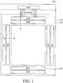
- FIG. 1 is a view schematically illustrating an organic light emitting display device including an electrostatic discharging circuit according to an exemplary embodiment of the present disclosure.
- an organic light emitting display device 100 includes an active area on a substrate 110 which is a display area and includes a driving voltage line VDD which is connected to a pad unit PAD, a gate driving unit GIP, and an electrostatic discharging circuit ESD for minimizing damages due to static electricity which may be generated in the organic light emitting display device 100. Further, the organic light emitting display device 100 includes a bending area between the pad unit PAD and the active area so that the pad unit PAD is folded to a rear surface of the organic light emitting display device 100 to minimize the non-display area such as a pad unit PAD, but is not limited thereto.
- the electrostatic discharging circuit ESD may be configured to be connected to the gate driving unit GIP and/or the driving voltage line VDD and may be disposed to enclose the active area.
- FIG. 1 as an example, it is illustrated that the organic light emitting display device 100 has a rectangular shape and the electrostatic discharging circuits ESD are disposed on the upper, lower, left, and right sides, but the shape of the organic light emitting display is not limited thereto.
- the organic light emitting display device 100 may be a circular display device or various types of display device such as an electric signboard of a vehicle.
- an organic light emitting diode including an organic light emitting layer and at least one driving element for controlling the driving of the organic light emitting diode and the driving element is disposed to be connected to the driving voltage line VDD and the gate driving unit GIP.
- an encapsulation layer 120 is disposed to cover the active area to protect the organic light emitting diode from penetration of oxygen and moisture.
- the encapsulation layer 120 is disposed to minimize the permeation of oxygen and moisture as described above and is disposed to also cover the electrostatic discharging circuit ESD, the gate driving unit GIP, and the driving voltage line VDD.
- the encapsulation layer 120 may be an encapsulation layer formed of an inorganic material and may have a multi-layered structure formed of two or more layers including an organic material.
- the electrostatic discharging circuit ESD discharges static electricity accumulated in the organic light emitting display device 100
- the encapsulation layer 120 formed of the inorganic material may be damaged.
- the protective layer 130 covers the electrostatic discharging circuit ESD to minimize damages to be generated during the process of discharging static electricity.
- the defect due to electrical corrosion of a wiring electrode caused by abnormal voltage and current which may be generated in the electrostatic discharging circuit ESD may be minimized.
- FIG. 2 is a view schematically illustrating an electrical connection relationship of an organic light emitting display device including an electrostatic discharging circuit according to an exemplary embodiment of the present disclosure.
- the organic light emitting display device 100 includes a gate driving unit GIP and a data driving unit 200 which are panel driving units.
- the data driving unit 200 converts image data supplied from a timing controller (not illustrated) into an analog data signal using gamma voltages and supplies the analog data signal to data lines DL.
- the data driving unit 200 supplies a reference voltage to a reference line RL.
- the data driving unit 200 may supply a high potential power supply voltage EVDD, a low potential power supply voltage EVSS, and a ground voltage GND supplied from a power supply unit (not illustrated) to the display panel 100.
- the gate driving unit GIP drives a plurality of gate lines GL in accordance with gate control signals from the timing controller (not illustrated).
- the gate driving unit GIP supplies a scan pulse of a gate-on voltage to each gate line GL during a scan period and supplies a gate-off voltage during the remaining period.
- the gate driving unit GIP is on a thin film transistor array substrate together with thin film transistors which configure the pixels P of the pixel array in an inactive area to be embedded.
- switching elements which configure the gate driving unit GIP a poly-TFT or an oxide TFT having a coplanar structure in which source and drain electrodes do not overlap the gate electrode may be used to reduce a parasitic capacitance.
- the organic light emitting display device 100 displays images through a matrix type pixel array. Each pixel P of the pixel array is independently driven by the TFT.
- TFT an amorphous silicon (a-Si) TFT, a poly silicon (poly-Si) TFT, an oxide TFT, or an organic TFT may be used.
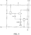
- FIG. 3 is an equivalent circuit diagram illustrating a configuration of one pixel illustrated in FIG. 2 .
- Each pixel includes an OLED element connected between the high potential power supply (EVDD) line and a low potential power supply (EVSS) line and a pixel circuit which includes first and second switching TFTs ST1 and ST2 and a driving TFT (DT) for independently driving the OLED element and a storage capacitor Cst.
- the pixel circuit has various configurations so that it is not limited to the structure of FIG. 3 .
- the OLED element includes an anode connected to the driving TFT (DT), a cathode connected to the low potential power supply EVSS, and a light emitting layer between the anode and the cathode to generate light which is proportional to an amount of current supplied from the driving TFT (DT).
- the first switching TFT (ST1) is driven by a gate signal of one gate line GLa to supply the data voltage from the data line DL to a gate node of the driving TFT (DT) and the second switching TFT (ST2) is driven by a gate signal of another gate line GLb to supply a reference voltage from the reference line RL to a source node of the driving TFT (DT).
- the second switching TFT (ST2) is used as a path which outputs the current from the driving TFT (DT) to the reference line RL in a sensing mode.
- the storage capacitor Cst connected between the gate electrode and the source electrode of the driving TFT (DT) charges a different voltage between a data voltage supplied to the gate electrode of the driving TFT (DT) through the first switching TFT (ST1) and a reference voltage supplied to the source electrode of the driving TFT (DT) through the second switching TFT (ST2) and supplies the charged voltage as a driving voltage of the driving TFT (DT) during a period when the first and second switching TFTs ST1 and ST2 are turned off.
- the driving TFT controls the current supplied from the high potential power supply EVDD in accordance with a driving voltage supplied from the storage capacitor Cst to supply the current proportional to the driving voltage to the OLED element.
- the OLED element emits light.
- the electrostatic discharging circuit ESD is connected to each of the wiring lines including a gate line GL, a data line DL, a reference line RL, and a power line PL.
- the electrostatic discharging circuit ESD is turned on to discharge the static electricity to the ground line to block the static electricity.
- FIG. 4 is an equivalent circuit diagram illustrating a configuration of an electrostatic discharging circuit illustrated in FIG. 2 .
- the electrostatic discharging circuit ESD connected between each gate line GL and the ground line GND includes a thin film transistor T1, a first capacitor C1 between a gate electrode GE of the thin film transistor T1 and a first electrode E1 and a second capacitor C2 between the gate electrode GE and a second electrode E2.
- One of the first and second electrodes E1 and E2 is a source electrode and the other one is a drain electrode.
- the scan output is not supplied to the gate electrode GE which is in a floating state by the first and second capacitors C1 and C2 so that the thin film transistor T1 is maintained to be turned off.
- a channel width of the thin film transistor T1 is smaller than a channel length to increase the resistance of the channel.
- FIG. 5 is a schematic cross-sectional view taken along the line A-A' of FIG. 1 for explaining a protective layer according to an exemplary embodiment of the present disclosure
- FIG. 6 is a schematic cross-sectional view taken along the line B-B' of FIG. 1 for explaining a protective layer according to an exemplary embodiment of the present disclosure.
- FIGS. 5 and 6 A configuration of an organic light emitting display device including an electrostatic discharging circuit ESD covered by a protective layer 130 will be described with reference to FIGS. 5 and 6 and the previous drawings are also referenced.
- the organic light emitting display device 100 includes a driving element TFT disposed on a substrate 110, an organic light emitting layer EL, a plurality of wiring electrodes 150, 151, and 152 connected to the driving element TFT, an electrostatic discharging circuit ESD electrically connected to the wiring electrodes 150, 151, and 152, and a gate driving unit GIP.
- the substrate 110 an active area is defined and even though it is simply illustrated, a plurality of organic light emitting diodes is disposed to configure a plurality of pixels. Further, the substrate 110 includes a plurality of driving elements TFTs to supply a signal and current for driving the plurality of pixels to the pixels. For example, a switching thin film transistor, a driving element TFT connected to the switching thin film transistor, and an organic light emitting diode connected to the driving element TFT are disposed on the substrate 110.
- the driving elements TFTs such as the switching thin film transistor and the driving element are disposed to be connected to the gate line GL and the data line DL disposed on the substrate 110.
- the switching thin film transistor serves to select a pixel and is disposed in a portion where the gate line GL and the data line DL intersect each other.
- the switching thin film transistor includes a gate electrode GE, a semiconductor layer, a source electrode, and a drain electrode.
- the driving element TFT serves to drive an anode electrode AND of a pixel selected by the switching thin film transistor.
- the driving element TFT includes a gate electrode GE connected to a drain electrode of the switching thin film transistor, an active layer AE, a source electrode SD connected to a driving current wiring line, and a drain electrode SD.
- the drain electrode SD of the driving element TFT is connected to the anode electrode AND which is a pixel electrode of the organic light emitting diode.
- the above-described driving element TFT is disposed on a buffer layer 111 on the substrate 110.
- the buffer layer 111 minimizes penetration of moisture or impurities through the substrate 110 and planarizes an upper portion of the substrate 110.
- the buffer layer 111 is not an essential component. Whether to form the buffer layer 111 is determined based on a type of the substrate 110 or a type of the driving element TFT.
- the driving element TFT is on the buffer layer 111 and supplies signals and current to the organic light emitting diode.
- the driving element TFT includes an active layer AE, a gate electrode GE, a source electrode SD, and a drain electrode SD.
- the active layer AE is on the buffer layer 111 and a gate insulating layer 112 is on the active layer AE to insulate the active layer AE and the gate electrode GE from each other.
- the gate electrode GE is on the gate insulating layer 112 to overlap the active layer AE and an interlayer insulating layer 113 is on the gate electrode GE and the gate insulating layer 112.
- the source electrode SD and the drain electrode SD are on the interlayer insulating layer 113.
- the source electrode SD and the drain electrode SD are electrically connected to the active layer AE.
- the active layer AE may be formed of amorphous silicon (a-Si), polycrystalline silicon (poly-Si), an oxide semiconductor, or an organic semiconductor.
- the active layer 132 may be formed of ITO, IZO, indium gallium zinc oxide (IGZO), or indium tin zinc oxide (ITZO), but is not limited thereto.
- IGZO indium gallium zinc oxide
- ITZO indium tin zinc oxide
- a ratio of In:Ga:Zn may be 1:2:1.
- a Ga rich layer which reduces PBTS may be formed on an upper surface of the IGZO layer in the active layer AE.
- the organic light emitting display device 100 may further include a switching thin film transistor or a capacitor for driving the organic light emitting diode. Further, in the specification, even though it is described that the driving element TFT has a coplanar structure, an inverted staggered thin film transistor may also be used.
- the anode AND of the organic light emitting diode may be connected to the source electrode SD of the driving element TFT depending on a design.
- a planarization layer 114 is disposed on the driving element TFT.
- the planarization layer 114 is a layer which planarizes an upper portion of the substrate 110 and is formed of an organic insulating material to cover an upper step of the substrate 110.
- the planarization layer 114 may be configured by one layer or may have a double layered structure formed of at least two organic insulating materials. Further, the planarization layer 114 includes a contact hole to be electrically connected to the anode AND of the organic light emitting diode.
- the organic light emitting diode is disposed on the planarization layer 114 and includes an anode AND, an organic layer EL, and a cathode CE. Even though only one organic light emitting diode is illustrated in FIGS. 5 and 6 , a plurality of organic light emitting diodes may be disposed so as to correspond to a plurality of pixel areas of the light emitting display device 100.
- the anode AND is an electrode which supplies holes to the organic layer EL and may be configured by a transparent conductive material having a high work function.
- the transparent conductive material may include ITO, IZO, or ITZO, but is not limited thereto.
- the anode AND may further include a reflector or may include a material having higher reflectance.
- the anode AND may also be referred to as a pixel electrode.
- the cathode CE is an electrode which supplies electrons to the organic layer EL and may be configured by a metal having a relatively low work function, for example, silver, titanium (Ti), aluminum, molybdenum (Mo) or an alloy (Ag:Mg) of silver and magnesium.
- the cathode CE may also be referred to as a common electrode.
- a content of silver is higher than a content of magnesium to lower resistance of the cathode CE.
- a ytterbium (Yb) layer may be disposed above, below, or above and below the Ag:Mg layer.
- the organic layer EL is disposed between the anode AND and the cathode CE.
- the organic layer EL includes an organic light emitting layer.
- the organic light emitting layer has a patterned emission layer structure.
- light emitting layers which emits light of different colors are separately formed for every pixel.
- a red organic light emitting layer emitting red light, a green organic light emitting layer emitting green light, and a blue organic light emitting layer emitting blue light may be separately formed in a red sub pixel, a green sub pixel, and a blue sub pixel, respectively.
- the red sub pixel, the green sub pixel, and the blue sub pixel may configure one pixel.
- each of the red organic light emitting layer, the green organic light emitting layer, and the blue organic light emitting layer holes and electrons supplied through the anode AND and the cathode CE are coupled to each other to emit light.
- Each of the organic light emitting layers may be deposited as a pattern using a mask which is open for every pixel, for example, a fine metal mask (FMM), but is not limited thereto and the organic light emitting layer may be commonly formed in all the sub pixels on the substrate 110.
- the organic light emitting layer may be formed of a material emitting white light and a color filter may be disposed to correspond to an area where the organic light emitting layer emits light.
- the organic layers may further include organic layers, such as an injecting layer or a transporting layer, for improving a light emission efficiency of the organic light emitting diode. At least some of organic layers may have a common structure to be commonly disposed for a plurality of sub pixels, in order to achieve an advantage during a manufacturing process.
- the organic layer having the common structure may be formed using a common mask in which all sub pixels are opened.
- the layer having the common structure may be laminated with the same structure in all the sub pixels without having a pattern for every sub pixel. That is, the organic layer having the common structure is disposed to be connected or extend to an adjacent sub pixel from one sub pixel without having a disconnected portion and is shared by a plurality of sub pixels.
- a hole injection layer or a hole transport layer may further disposed between the anode AND and the cathode CE for smoothly moving the holes.
- the hole injection layer or the hole transport layer may have a common structure to be commonly disposed in the plurality of sub pixels.
- the hole transport layer may be configured by a p-type hole transport layer on which a p-type dopant is doped.
- a bank layer 115 is disposed to define sub pixels and exposes a part of a top surface of the anode AND. Specifically, the bank layer 115 may be disposed to cover an edge of the anode AND.
- the bank layer 115 is formed of an insulating material to insulate anodes of the adjacent sub pixels from each other. According to several exemplary embodiments, the bank layer 115 may be configured of a black bank having a high optical absorbance to prevent color mixture between adjacent sub pixels.
- a spacer 116 may be disposed on the bank layer 115.
- the spacer 116 is used to support a load of a metal mask such as FMM during a process of disposing the above-described organic light emitting layer and may be formed of the same material as the bank layer 115.
- a capping layer CPL which represent a protection layer and which covers the above-described organic light emitting diode may be disposed.
- the capping layer CPL may include a particulate absorbent or particles for photo-extraction and may be disposed to cover the organic light emitting diode.
- An encapsulation layer 120 is disposed on the capping layer CPL to minimize penetration of moisture and oxygen.
- the encapsulation layer 120 is disposed to cover the entire active area and is disposed to cover the electrostatic discharging circuit ESD, the gate driving unit GIP, and the wiring electrodes 150, 151, and 152.
- a bending area BA may be defined.
- the wiring electrodes 150, 151, and 152 are disposed to form an electrical connection relationship with the pad unit PAD.
- the wiring electrodes 150, 151, and 152 open in the bending area BA may be covered by a wiring electrode protecting layer 131 to prevent oxidation thereof.
- the wiring electrodes 150, 151, and 152 are connected to the above-described driving element TFT and is disposed using an electrode such as the source electrode SD or the gate electrode GE. Further, the wiring electrodes 150, 151, and 152 are connected to the electrostatic discharging circuit ESD and the electrostatic discharging circuit ESD may be configured by the same material as the electrode and the semiconductor which form the driving element TFT.
- the electrostatic discharging circuit ESD is covered by the encapsulation layer 120 and the protective layer 130 described above.
- the protective layer 130 may be disposed with the same material as the planarization layer 114 and may be an organic layer formed of an organic material and may be at least one multilayered structure.
- the electrostatic discharging circuit ESD discharges static electricity accumulated in the organic light emitting display device 100, the encapsulation layer 120 may be physically damaged. In order to minimize the physical damage, the electrostatic discharging circuit ESD is covered by the above-described protective layer 130.
- the electrostatic discharging circuit ESD may be configured by the same material as the above-described source electrode SD or gate electrode GE. However, during the process of discharging static electricity, electrical corrosion may be caused. The side effects due to the electrical corrosion are absorbed by the protective layer 130 so that the spreading of the side effects to an area where the driving element TFT and the organic light emitting diode are provided may be minimized.
- minute crack due to a physical damage which may be caused in another component during the process of discharging static electricity may be minimized by the electrostatic discharging circuit ESD covered by the protective layer 130, so that a moisture penetration path generated due to the minute crack may be minimized.
- the substrate 110 may include a bending area BA.
- the wiring electrode 150 is disposed in the bending area BA to be connected to the pad unit PAD and the electrostatic discharging circuit ESD.
- the encapsulation layer 120 on the wiring electrode 150 disposed in the bending area BA is open to prevent the crack from being generated on the encapsulation layer 120 while the substrate 110 is bent.
- the wiring electrode protecting layer 131 is disposed on the wiring electrode 150 disposed in the bending area BA to prevent corrosion of the wiring electrode 150 due to the electrical corrosion and stress when the substrate 110 is bent to prevent the crack on the wiring electrode 150.
- the wiring electrode protecting layer 131 may be formed of an organic insulating material and may be formed of the same material as the planarization layer 114 and the protective layer 130. However, the wiring electrode protecting layer 131 is disposed to be isolated from the protective layer 130 and the planarization layer 114 so that even though a moisture penetration path is generated, the spreading of the moisture penetration path may be prevented.
- an organic light emitting display device includes at least one driving element which is connected to a data line and a gate line on a substrate, a planarization layer which covers the driving element; an organic light emitting diode which is disposed on the planarization layer and is connected to the driving element; and an electrostatic discharging circuit which is connected to the data line or the gate line, in which the electrostatic discharging circuit is covered by a protective layer.
- the planarization layer and the protective layer may include at least one organic layer.
- the organic layers included in the planarization layer and the protective layer may be isolated from each other.
- the substrate may be a flexible substrate in which a bending area is defined.
- the organic light emitting display device may further include an encapsulation layer which covers the organic light emitting diode and the protective layer and in the bending area, the encapsulation layer may be open.
- the organic light emitting display device may further include a wiring electrode in the bending area and the wiring electrode may be the same material as an electrode selected from electrodes which configure the driving element.
- the organic light emitting display device may further include a wiring electrode protecting layer which covers the wiring electrode.
- the wiring electrode protecting layer and the protective layer may be isolated from each other.
- the wiring electrode protecting layer may include at least one organic layer.
- the wiring electrode may be connected to the electrostatic discharging circuit.
Landscapes
- Physics & Mathematics (AREA)
- Optics & Photonics (AREA)
- Engineering & Computer Science (AREA)
- Microelectronics & Electronic Packaging (AREA)
- Chemical & Material Sciences (AREA)
- Inorganic Chemistry (AREA)
- Electroluminescent Light Sources (AREA)
- Devices For Indicating Variable Information By Combining Individual Elements (AREA)
- Geometry (AREA)
Abstract
Description
- This application claims the priority of Korean Patent Application No.
10-2017-0110783 filed on August 31, 2017 - The present disclosure relates to an organic light emitting display device which includes a protective layer for protecting an electrostatic discharging circuit for minimizing damages of the organic light emitting display device due to static electricity, and more particularly, to an organic light emitting display device which protects an electrostatic discharging circuit.
- Examples of the display device include a liquid crystal display (LCD), an organic light emitting diode (OLED), an electrophoretic display (EPD), and an electro wetting display.
- The display device includes a display panel which displays images through a pixel array in which pixels are independently driven by thin film transistors (TFT) and a gate driving unit and a data driving unit which drive the display panel. Recently, the gate driving unit mainly uses a gate in panel (GIP) technology in which the gate driving unit is formed together with a TFT array of the pixel array to be embedded or located in a non-display area of the display panel.
- Further, in recent years, various forms and functions of the display device are demanded and in order to implement various forms and functions, a substrate formed of a plastic material such as polyimide is used as a flexible substrate.
- An organic light emitting display device is mainly used as the display device having various forms and functions. The organic light emitting display device has advantages in that a separate light source is unnecessary, low-power driving is allowed, and various shapes of display area can be disposed on various shapes of substrate.
- However, in the organic light emitting display device, since an organic material is used for a light emitting layer, it is disadvantageous in that it is vulnerable to penetration of oxygen and moisture. Thus, in order to compensate the disadvantage, an encapsulation layer which may minimize the penetration of oxygen and moisture is disposed on the organic light emitting diode to protect the organic light emitting layer.
- A moisture penetration path may be generated due to various influences by various components included in the display device. As some examples thereof, minute cracks may be generated in the encapsulation layer which protects the organic light emitting layer, due to a discharge phenomenon which may be generated in the electrostatic discharging circuit of the display device. Such minute cracks undesirably provide a path which oxygen and moisture penetrate into the organic light emitting layer. Further, an electrode which connects components disposed at an outer periphery of the display area, such as an electrostatic discharging circuit, may be oxidized or electrically corroded by the flow of current. Thus, the moisture penetration path may be undesirably generated due to the oxidation or electrical corrosion.
- A thin film encapsulation technique which alternately laminates inorganic layers and organic layers is used to seal the organic light emitting diode. As an inorganic layer for the thin film encapsulation technique, an oxide layer such as aluminum oxide (AlOx) which may secure excellent barrier property even with a small thickness is mainly used. Specifically, since the smaller the thickness of the thin film encapsulation, the better the flexibility of the organic light emitting display device, an oxide layer may be advantageously used for an inorganic layer of the thin film encapsulation to implement a flexible organic light emitting display device. However, as described above, during the process of discharging static electricity through the electrostatic discharging circuit, the encapsulation layer disposed above the electrostatic discharging circuit may be minutely cracked due to excessively concentrated current. Thus, a moisture penetration path may be generated due to minute cracks. Further, the moisture penetration path may be generated due to oxidation or electrical corrosion which may be generated in an electrode which configures the electrostatic discharging circuit.
- Accordingly, embodiments of the present disclosure are directed to an organic light emitting display device that substantially obviates one or more of the problems due to limitations and disadvantages of the related art.
- Accordingly, an object of the present disclosure is to provide an organic light emitting display device with an improved reliability by minimizing a moisture penetration path which may be generated in the electrostatic discharging circuit.
- Another object of the present disclosure is to provide an organic light emitting display device which may minimize damages of an encapsulation layer due to a discharging activity which may be generated in the electrostatic discharging circuit.
- Additional features and aspects will be set forth in the description that follows, and in part will be apparent from the description, or may be learned by practice of the inventive concepts provided herein. Other features and aspects of the inventive concepts may be realized and attained by the structure particularly pointed out in the written description, or derivable therefrom, and the claims hereof as well as the appended drawings.
- The object is solved by the features of the independent claims. Preferred embodiments are given in the dependent claims.
- To achieve these and other aspects of the inventive concepts, as embodied and broadly described, an organic light emitting display device comprises a data line and a gate line disposed on a substrate and at least one driving element which operates to transmit current and signals to an organic light emitting diode in response to signals transmitted from the data line and the gate line. The organic light emitting diode is disposed on a planarization layer and the planarization layer is disposed to cover the driving element, the data line, and the gate line so as to dispose the organic light emitting diode. Further, in order to minimize the damages of the display device due to static electricity, an electrostatic discharging circuit connected to the data line and the gate line is disposed. The electrostatic discharging circuit is covered by a protective layer to minimize influence due to the discharging of static electricity and thus improve the lifespan reliability of the display device.
- According to the exemplary embodiment of the present disclosure, a protective layer which covers an electrostatic discharging circuit is equipped to improve lifespan reliability for static electricity of an organic light emitting display device. Further, the influence of the static electricity is minimized by using the protective layer to improve a display quality of the organic light emitting display device.
- In some embodiments the organic light emitting display device may comprise at least one driving element which is connected to a data line and a gate line on a substrate; a planarization layer which covers the driving element; an organic light emitting diode which is disposed on the planarization layer and is connected to the driving element; and an electrostatic discharging circuit which is connected to the data line or the gate line, wherein the electrostatic discharging circuit is covered by a protective layer.
- Preferably, the planarization layer and the protective layer may include at least one organic layer.
- Preferably, the planarization layer and the protective layer may be isolated from each other.
- Preferably, the organic layers included in the planarization layer and the protective layer may be isolated and/or spaced apart from each other.
- Preferably, the substrate may be a flexible substrate.
- Preferably, the substrate includes a bending area.
- Preferably, the organic light emitting display device may further comprise an encapsulation layer which covers the organic light emitting diode and the protective layer.
- Preferably, in the bending area, the encapsulation layer may be opened or removed.
- Preferably, the encapsulation layer is contacting an interlayer insulating layer between the electrostatic discharging circuit and the organic light emitting diode.
- Preferably, the organic light emitting display device may further comprise a wiring electrode in the bending area and/or in the area of the gate driving unit.
- Preferably, the wiring electrode may be the same material as an electrode selected from electrodes which configure the driving element.
- Preferably, the organic light emitting display device may further comprise a wiring electrode protecting layer which may cover the wiring electrode.
- Preferably, the wiring electrode protecting layer is covering the wiring electrode in the bending area and/or in the area of the gate driving unit.
- Preferably, the wiring electrode protecting layer and the protective layer may be isolated and/or spaced apart from each other.
- Preferably, the wiring electrode protecting layer may include at least one organic layer.
- Preferably, the wiring electrode may be connected to the electrostatic discharging circuit.
- In another aspect a display device is provided, comprising an electrostatic discharging circuit is disposed on a substrate and connected to a driving element with a data line or a gate line; a planarization layer cover the driving element, an organic light emitting diode on the planarization layer; and a protective layer covering the organic light emitting diode and the electrostatic discharging circuit, wherein the protective layer covering the electrostatic discharging circuit is isolated from the protective layer covering the organic light emitting diode.
- Preferably, the protective layer covering the organic light emitting diode is a capping layer.
- Preferably, the substrate may be a flexible substrate in which a bending area is included.
- Preferably, the bending area further comprises a wiring electrode and the protective layer covering the wiring electrode but isolated from the protective layer covering the electrostatic discharging circuit.
- Preferably, the display apparatus may further comprise an encapsulation layer on the organic layer, electrostatic discharge circuit and the wiring electrode.
- Preferably, the encapsulation layer on the electrostatic discharging circuit may be isolated from the encapsulation layer on the organic emitting layer and the wiring electrode.
- Preferably, the encapsulation layer may further comprise at least one organic sub layer, wherein the organic sub layer on the electrostatic discharge circuit is isolated from the sub layer on the organic emitting layer and the wiring electrode.
- Objects of the present disclosure are not limited to the above-mentioned objects, and other objects, which are not mentioned above, can be clearly understood by those skilled in the art from the following descriptions.
- The objects to be achieved by the present disclosure, the means for achieving the objects, and effects of the present disclosure described above do not specify essential features of the claims, and, thus, the scope of the claims is not limited to the disclosure of the present disclosure.
- It is to be understood that both the foregoing general description and the following detailed description are exemplary and explanatory and are intended to provide further explanation of the inventive concepts as claimed.
- The accompanying drawings, which are included to provide a further understanding of the disclosure and are incorporated and constitute a part of this application, illustrate embodiments of the disclosure and together with the description serve to explain various principles. In the drawings:
-
FIG. 1 is a view schematically illustrating an organic light emitting display device including an electrostatic discharging circuit according to an exemplary embodiment of the present disclosure; -
FIG. 2 is a view schematically illustrating an electrical connection relationship of an organic light emitting display device including an electrostatic discharging circuit according to an exemplary embodiment of the present disclosure; -
FIG. 3 is an equivalent circuit diagram illustrating a configuration of one pixel illustrated inFIG. 2 ; -
FIG. 4 is an equivalent circuit diagram illustrating a configuration of an electrostatic discharging circuit illustrated inFIG. 2 ; -
FIG. 5 is a schematic cross-sectional view taken along the line A-A' ofFIG. 1 for explaining a protective layer according to an exemplary embodiment of the present disclosure; and -
FIG. 6 is a schematic cross-sectional view taken along the line B-B' ofFIG. 1 for explaining a protective layer according to an exemplary embodiment of the present disclosure. - Advantages and characteristics of the present disclosure and a method of achieving the advantages and characteristics will be clear by referring to exemplary embodiments described below in detail together with the accompanying drawings. However, the present disclosure is not limited to the exemplary embodiments disclosed herein but will be implemented in various forms. The exemplary embodiments are provided by way of example only so that a person of ordinary skilled in the art can fully understand the disclosures of the present disclosure and the scope of the present disclosure. Thus, the present disclosure will be defined only by the scope of the appended claims.
- The shapes, sizes, ratios, angles, numbers, and the like illustrated in the accompanying drawings for describing the exemplary embodiments of the present disclosure are merely examples, and the present disclosure is not limited thereto. Like reference numerals generally denote like elements throughout the specification. Further, in the following description, a detailed explanation of known related technologies may be omitted to avoid unnecessarily obscuring the subject matter of the present disclosure. The terms such as "including," "having," and "consist of' used herein are generally intended to allow other components to be added unless the terms are used with the term "only". Any references to singular may include plural unless expressly stated otherwise.
- Components are interpreted to include an ordinary error range even if not expressly stated.
- When the position relation between two parts is described using the terms such as "on", "above", "below", and "next", one or more parts may be positioned between the two parts unless the terms are used with the term "immediately" or "directly".
- When the relation of a time sequential order is described using the terms such as "after", "continuously to", "next to", and "before", the order may not be continuous unless the terms are used with the term "immediately" or "directly".
- When the signal flowing relation is described, for example, when it is described that a signal is transmitted from a node A to a node B, the signal may be transmitted from the node A to the node B via another node unless the terms are used with the term "immediately" or "directly".
- Although the terms "first", "second", and the like are used for describing various components, these components are not confined by these terms. These terms are merely used for distinguishing one component from the other components. Thus, a first component to be mentioned below may be a second component in a technical concept of the present disclosure.
- The features of various embodiments of the present disclosure can be partially or entirely bonded to or combined with each other and can be interlocked and operated in technically various ways, and the embodiments can be carried out independently of or in association with each other.
- Hereinafter, various configurations and exemplary embodiments of an organic light emitting display including an electrostatic discharging circuit according to an exemplary embodiment of the present disclosure will be described with reference to the accompanying drawings.
-
FIG. 1 is a view schematically illustrating an organic light emitting display device including an electrostatic discharging circuit according to an exemplary embodiment of the present disclosure. - Referring to
FIG. 1 , even though it is simply illustrated, an organic light emittingdisplay device 100 includes an active area on asubstrate 110 which is a display area and includes a driving voltage line VDD which is connected to a pad unit PAD, a gate driving unit GIP, and an electrostatic discharging circuit ESD for minimizing damages due to static electricity which may be generated in the organic light emittingdisplay device 100. Further, the organic light emittingdisplay device 100 includes a bending area between the pad unit PAD and the active area so that the pad unit PAD is folded to a rear surface of the organic light emittingdisplay device 100 to minimize the non-display area such as a pad unit PAD, but is not limited thereto. - The electrostatic discharging circuit ESD may be configured to be connected to the gate driving unit GIP and/or the driving voltage line VDD and may be disposed to enclose the active area. In
FIG. 1 , as an example, it is illustrated that the organic light emittingdisplay device 100 has a rectangular shape and the electrostatic discharging circuits ESD are disposed on the upper, lower, left, and right sides, but the shape of the organic light emitting display is not limited thereto. The organic light emittingdisplay device 100 may be a circular display device or various types of display device such as an electric signboard of a vehicle. - Even though it is not illustrated in the active area, there are an organic light emitting diode including an organic light emitting layer and at least one driving element for controlling the driving of the organic light emitting diode and the driving element is disposed to be connected to the driving voltage line VDD and the gate driving unit GIP.
- As described above, in the organic light emitting diode and the organic light emitting layer in the active area, a defect such as a dark spot may be generated due to moisture and oxygen. Thus, an
encapsulation layer 120 is disposed to cover the active area to protect the organic light emitting diode from penetration of oxygen and moisture. - The
encapsulation layer 120 is disposed to minimize the permeation of oxygen and moisture as described above and is disposed to also cover the electrostatic discharging circuit ESD, the gate driving unit GIP, and the driving voltage line VDD. Theencapsulation layer 120 may be an encapsulation layer formed of an inorganic material and may have a multi-layered structure formed of two or more layers including an organic material. - While the electrostatic discharging circuit ESD discharges static electricity accumulated in the organic light emitting
display device 100, theencapsulation layer 120 formed of the inorganic material may be damaged. Thus, theprotective layer 130 covers the electrostatic discharging circuit ESD to minimize damages to be generated during the process of discharging static electricity. Alternatively, the defect due to electrical corrosion of a wiring electrode caused by abnormal voltage and current which may be generated in the electrostatic discharging circuit ESD may be minimized. -
FIG. 2 is a view schematically illustrating an electrical connection relationship of an organic light emitting display device including an electrostatic discharging circuit according to an exemplary embodiment of the present disclosure. - Referring to
FIG. 2 , the organic light emittingdisplay device 100 includes a gate driving unit GIP and adata driving unit 200 which are panel driving units. - The
data driving unit 200 converts image data supplied from a timing controller (not illustrated) into an analog data signal using gamma voltages and supplies the analog data signal to data lines DL. Thedata driving unit 200 supplies a reference voltage to a reference line RL. Thedata driving unit 200 may supply a high potential power supply voltage EVDD, a low potential power supply voltage EVSS, and a ground voltage GND supplied from a power supply unit (not illustrated) to thedisplay panel 100. - The gate driving unit GIP drives a plurality of gate lines GL in accordance with gate control signals from the timing controller (not illustrated). The gate driving unit GIP supplies a scan pulse of a gate-on voltage to each gate line GL during a scan period and supplies a gate-off voltage during the remaining period. The gate driving unit GIP is on a thin film transistor array substrate together with thin film transistors which configure the pixels P of the pixel array in an inactive area to be embedded. As switching elements which configure the gate driving unit GIP, a poly-TFT or an oxide TFT having a coplanar structure in which source and drain electrodes do not overlap the gate electrode may be used to reduce a parasitic capacitance.
- The organic light emitting
display device 100 displays images through a matrix type pixel array. Each pixel P of the pixel array is independently driven by the TFT. As the TFT, an amorphous silicon (a-Si) TFT, a poly silicon (poly-Si) TFT, an oxide TFT, or an organic TFT may be used. -
FIG. 3 is an equivalent circuit diagram illustrating a configuration of one pixel illustrated inFIG. 2 . - Each pixel includes an OLED element connected between the high potential power supply (EVDD) line and a low potential power supply (EVSS) line and a pixel circuit which includes first and second switching TFTs ST1 and ST2 and a driving TFT (DT) for independently driving the OLED element and a storage capacitor Cst. However, the pixel circuit has various configurations so that it is not limited to the structure of
FIG. 3 . - The OLED element includes an anode connected to the driving TFT (DT), a cathode connected to the low potential power supply EVSS, and a light emitting layer between the anode and the cathode to generate light which is proportional to an amount of current supplied from the driving TFT (DT).
- The first switching TFT (ST1) is driven by a gate signal of one gate line GLa to supply the data voltage from the data line DL to a gate node of the driving TFT (DT) and the second switching TFT (ST2) is driven by a gate signal of another gate line GLb to supply a reference voltage from the reference line RL to a source node of the driving TFT (DT). The second switching TFT (ST2) is used as a path which outputs the current from the driving TFT (DT) to the reference line RL in a sensing mode.
- The storage capacitor Cst connected between the gate electrode and the source electrode of the driving TFT (DT) charges a different voltage between a data voltage supplied to the gate electrode of the driving TFT (DT) through the first switching TFT (ST1) and a reference voltage supplied to the source electrode of the driving TFT (DT) through the second switching TFT (ST2) and supplies the charged voltage as a driving voltage of the driving TFT (DT) during a period when the first and second switching TFTs ST1 and ST2 are turned off.
- The driving TFT (DT) controls the current supplied from the high potential power supply EVDD in accordance with a driving voltage supplied from the storage capacitor Cst to supply the current proportional to the driving voltage to the OLED element. Thus, the OLED element emits light.
- The electrostatic discharging circuit ESD is connected to each of the wiring lines including a gate line GL, a data line DL, a reference line RL, and a power line PL. When the static electricity flows through the wiring lines, the electrostatic discharging circuit ESD is turned on to discharge the static electricity to the ground line to block the static electricity.
-
FIG. 4 is an equivalent circuit diagram illustrating a configuration of an electrostatic discharging circuit illustrated inFIG. 2 . - Referring to
FIG. 4 , the electrostatic discharging circuit ESD connected between each gate line GL and the ground line GND includes a thin film transistor T1, a first capacitor C1 between a gate electrode GE of the thin film transistor T1 and a first electrode E1 and a second capacitor C2 between the gate electrode GE and a second electrode E2. One of the first and second electrodes E1 and E2 is a source electrode and the other one is a drain electrode. - When a normal scan output is supplied to the gate line GL, the scan output is not supplied to the gate electrode GE which is in a floating state by the first and second capacitors C1 and C2 so that the thin film transistor T1 is maintained to be turned off.
- When an abnormal voltage such as static electricity is applied to the gate line GL, a voltage is generated in the gate electrode GE by the first capacitor C1 and half of a voltage flowing through the gate line GL is supplied to the gate electrode GE by the first and second capacitors C1 and C2. Thus, the thin film transistor T1 is turned on to discharge the static electricity flowing into the gate line GL to the ground line GND.
- When the normal scan output is supplied to the gate line GL, in order to minimize a leakage current flowing through the electrostatic discharging circuit ESD, a channel width of the thin film transistor T1 is smaller than a channel length to increase the resistance of the channel.
-
FIG. 5 is a schematic cross-sectional view taken along the line A-A' ofFIG. 1 for explaining a protective layer according to an exemplary embodiment of the present disclosure andFIG. 6 is a schematic cross-sectional view taken along the line B-B' ofFIG. 1 for explaining a protective layer according to an exemplary embodiment of the present disclosure. - A configuration of an organic light emitting display device including an electrostatic discharging circuit ESD covered by a
protective layer 130 will be described with reference toFIGS. 5 and6 and the previous drawings are also referenced. - The organic light emitting
display device 100 includes a driving element TFT disposed on asubstrate 110, an organic light emitting layer EL, a plurality ofwiring electrodes wiring electrodes - In the
substrate 110, an active area is defined and even though it is simply illustrated, a plurality of organic light emitting diodes is disposed to configure a plurality of pixels. Further, thesubstrate 110 includes a plurality of driving elements TFTs to supply a signal and current for driving the plurality of pixels to the pixels. For example, a switching thin film transistor, a driving element TFT connected to the switching thin film transistor, and an organic light emitting diode connected to the driving element TFT are disposed on thesubstrate 110. - The driving elements TFTs such as the switching thin film transistor and the driving element are disposed to be connected to the gate line GL and the data line DL disposed on the
substrate 110. The switching thin film transistor serves to select a pixel and is disposed in a portion where the gate line GL and the data line DL intersect each other. The switching thin film transistor includes a gate electrode GE, a semiconductor layer, a source electrode, and a drain electrode. - The driving element TFT serves to drive an anode electrode AND of a pixel selected by the switching thin film transistor. The driving element TFT includes a gate electrode GE connected to a drain electrode of the switching thin film transistor, an active layer AE, a source electrode SD connected to a driving current wiring line, and a drain electrode SD. The drain electrode SD of the driving element TFT is connected to the anode electrode AND which is a pixel electrode of the organic light emitting diode.
- The above-described driving element TFT is disposed on a
buffer layer 111 on thesubstrate 110. Thebuffer layer 111 minimizes penetration of moisture or impurities through thesubstrate 110 and planarizes an upper portion of thesubstrate 110. However, thebuffer layer 111 is not an essential component. Whether to form thebuffer layer 111 is determined based on a type of thesubstrate 110 or a type of the driving element TFT. - The driving element TFT is on the
buffer layer 111 and supplies signals and current to the organic light emitting diode. The driving element TFT includes an active layer AE, a gate electrode GE, a source electrode SD, and a drain electrode SD. Specifically, the active layer AE is on thebuffer layer 111 and agate insulating layer 112 is on the active layer AE to insulate the active layer AE and the gate electrode GE from each other. Further, the gate electrode GE is on thegate insulating layer 112 to overlap the active layer AE and an interlayer insulatinglayer 113 is on the gate electrode GE and thegate insulating layer 112. The source electrode SD and the drain electrode SD are on theinterlayer insulating layer 113. The source electrode SD and the drain electrode SD are electrically connected to the active layer AE. - The active layer AE may be formed of amorphous silicon (a-Si), polycrystalline silicon (poly-Si), an oxide semiconductor, or an organic semiconductor. When the active layer 132 is formed of an oxide semiconductor, the active layer 132 may be formed of ITO, IZO, indium gallium zinc oxide (IGZO), or indium tin zinc oxide (ITZO), but is not limited thereto. When the active layer 132 is formed of IGZO, a ratio of In:Ga:Zn may be 1:2:1. In this case, a Ga rich layer which reduces PBTS may be formed on an upper surface of the IGZO layer in the active layer AE.
- In
FIGS. 5 and6 , for the convenience of description, among various thin film transistors which may be included in the organic light emittingdisplay device 100, only a driving element TFT connected to the anode AND of the organic light emitting diode is illustrated. However, the organic light emittingdisplay device 100 may further include a switching thin film transistor or a capacitor for driving the organic light emitting diode. Further, in the specification, even though it is described that the driving element TFT has a coplanar structure, an inverted staggered thin film transistor may also be used. Further, even though a structure in which the anode AND of the organic light emitting diode is connected to the drain electrode SD of the driving element TFT is illustrated, the anode AND of the organic light emitting diode may be connected to the source electrode SD of the driving element TFT depending on a design. - A
planarization layer 114 is disposed on the driving element TFT. Theplanarization layer 114 is a layer which planarizes an upper portion of thesubstrate 110 and is formed of an organic insulating material to cover an upper step of thesubstrate 110. Theplanarization layer 114 may be configured by one layer or may have a double layered structure formed of at least two organic insulating materials. Further, theplanarization layer 114 includes a contact hole to be electrically connected to the anode AND of the organic light emitting diode. - The organic light emitting diode is disposed on the
planarization layer 114 and includes an anode AND, an organic layer EL, and a cathode CE. Even though only one organic light emitting diode is illustrated inFIGS. 5 and6 , a plurality of organic light emitting diodes may be disposed so as to correspond to a plurality of pixel areas of the light emittingdisplay device 100. - The anode AND is an electrode which supplies holes to the organic layer EL and may be configured by a transparent conductive material having a high work function. The transparent conductive material may include ITO, IZO, or ITZO, but is not limited thereto. As illustrated in the drawing, when the organic light emitting
display device 100 is driven in a top emission manner, the anode AND may further include a reflector or may include a material having higher reflectance. Here, the anode AND may also be referred to as a pixel electrode. - The cathode CE is an electrode which supplies electrons to the organic layer EL and may be configured by a metal having a relatively low work function, for example, silver, titanium (Ti), aluminum, molybdenum (Mo) or an alloy (Ag:Mg) of silver and magnesium. Here, the cathode CE may also be referred to as a common electrode. When the cathode CE is configured by an alloy of silver and magnesium, a content of silver is higher than a content of magnesium to lower resistance of the cathode CE. In this case, in order to prevent silver from being oxidized and lowering the resistance, a ytterbium (Yb) layer may be disposed above, below, or above and below the Ag:Mg layer.
- The organic layer EL is disposed between the anode AND and the cathode CE. The organic layer EL includes an organic light emitting layer. The organic light emitting layer has a patterned emission layer structure. In this case, light emitting layers which emits light of different colors are separately formed for every pixel. For example, a red organic light emitting layer emitting red light, a green organic light emitting layer emitting green light, and a blue organic light emitting layer emitting blue light may be separately formed in a red sub pixel, a green sub pixel, and a blue sub pixel, respectively. In this case, the red sub pixel, the green sub pixel, and the blue sub pixel may configure one pixel. On each of the red organic light emitting layer, the green organic light emitting layer, and the blue organic light emitting layer, holes and electrons supplied through the anode AND and the cathode CE are coupled to each other to emit light. Each of the organic light emitting layers may be deposited as a pattern using a mask which is open for every pixel, for example, a fine metal mask (FMM), but is not limited thereto and the organic light emitting layer may be commonly formed in all the sub pixels on the
substrate 110. In this case, the organic light emitting layer may be formed of a material emitting white light and a color filter may be disposed to correspond to an area where the organic light emitting layer emits light. - The organic layers may further include organic layers, such as an injecting layer or a transporting layer, for improving a light emission efficiency of the organic light emitting diode. At least some of organic layers may have a common structure to be commonly disposed for a plurality of sub pixels, in order to achieve an advantage during a manufacturing process.
- Here, the organic layer having the common structure may be formed using a common mask in which all sub pixels are opened. The layer having the common structure may be laminated with the same structure in all the sub pixels without having a pattern for every sub pixel. That is, the organic layer having the common structure is disposed to be connected or extend to an adjacent sub pixel from one sub pixel without having a disconnected portion and is shared by a plurality of sub pixels.
- For example, in addition to the organic light emitting layer, a hole injection layer or a hole transport layer may further disposed between the anode AND and the cathode CE for smoothly moving the holes. The hole injection layer or the hole transport layer may have a common structure to be commonly disposed in the plurality of sub pixels. In several exemplary embodiments, the hole transport layer may be configured by a p-type hole transport layer on which a p-type dopant is doped.
- A
bank layer 115 is disposed to define sub pixels and exposes a part of a top surface of the anode AND. Specifically, thebank layer 115 may be disposed to cover an edge of the anode AND. Thebank layer 115 is formed of an insulating material to insulate anodes of the adjacent sub pixels from each other. According to several exemplary embodiments, thebank layer 115 may be configured of a black bank having a high optical absorbance to prevent color mixture between adjacent sub pixels. - A
spacer 116 may be disposed on thebank layer 115. Thespacer 116 is used to support a load of a metal mask such as FMM during a process of disposing the above-described organic light emitting layer and may be formed of the same material as thebank layer 115. - In the meantime, a capping layer CPL which represent a protection layer and which covers the above-described organic light emitting diode may be disposed. The capping layer CPL may include a particulate absorbent or particles for photo-extraction and may be disposed to cover the organic light emitting diode.
- An
encapsulation layer 120 is disposed on the capping layer CPL to minimize penetration of moisture and oxygen. Theencapsulation layer 120 is disposed to cover the entire active area and is disposed to cover the electrostatic discharging circuit ESD, the gate driving unit GIP, and thewiring electrodes - In the
substrate 110 which configures the organic light emittingdisplay device 100, a bending area BA may be defined. In the bending area, thewiring electrodes wiring electrodes electrode protecting layer 131 to prevent oxidation thereof. - The
wiring electrodes wiring electrodes - The electrostatic discharging circuit ESD is covered by the
encapsulation layer 120 and theprotective layer 130 described above. Theprotective layer 130 may be disposed with the same material as theplanarization layer 114 and may be an organic layer formed of an organic material and may be at least one multilayered structure. - While the electrostatic discharging circuit ESD discharges static electricity accumulated in the organic light emitting
display device 100, theencapsulation layer 120 may be physically damaged. In order to minimize the physical damage, the electrostatic discharging circuit ESD is covered by the above-describedprotective layer 130. - The electrostatic discharging circuit ESD may be configured by the same material as the above-described source electrode SD or gate electrode GE. However, during the process of discharging static electricity, electrical corrosion may be caused. The side effects due to the electrical corrosion are absorbed by the
protective layer 130 so that the spreading of the side effects to an area where the driving element TFT and the organic light emitting diode are provided may be minimized. - Further, as described above, minute crack due to a physical damage which may be caused in another component during the process of discharging static electricity may be minimized by the electrostatic discharging circuit ESD covered by the
protective layer 130, so that a moisture penetration path generated due to the minute crack may be minimized. - The
substrate 110 may include a bending area BA. Thewiring electrode 150 is disposed in the bending area BA to be connected to the pad unit PAD and the electrostatic discharging circuit ESD. Theencapsulation layer 120 on thewiring electrode 150 disposed in the bending area BA is open to prevent the crack from being generated on theencapsulation layer 120 while thesubstrate 110 is bent. However, the wiringelectrode protecting layer 131 is disposed on thewiring electrode 150 disposed in the bending area BA to prevent corrosion of thewiring electrode 150 due to the electrical corrosion and stress when thesubstrate 110 is bent to prevent the crack on thewiring electrode 150. - The wiring
electrode protecting layer 131 may be formed of an organic insulating material and may be formed of the same material as theplanarization layer 114 and theprotective layer 130. However, the wiringelectrode protecting layer 131 is disposed to be isolated from theprotective layer 130 and theplanarization layer 114 so that even though a moisture penetration path is generated, the spreading of the moisture penetration path may be prevented. - The exemplary embodiments of the present disclosure can also be described as follows:
- According to an aspect of the present disclosure, an organic light emitting display device includes at least one driving element which is connected to a data line and a gate line on a substrate, a planarization layer which covers the driving element; an organic light emitting diode which is disposed on the planarization layer and is connected to the driving element; and an electrostatic discharging circuit which is connected to the data line or the gate line, in which the electrostatic discharging circuit is covered by a protective layer.
- The planarization layer and the protective layer may include at least one organic layer.
- The organic layers included in the planarization layer and the protective layer may be isolated from each other.
- The substrate may be a flexible substrate in which a bending area is defined.
- The organic light emitting display device may further include an encapsulation layer which covers the organic light emitting diode and the protective layer and in the bending area, the encapsulation layer may be open.
- The organic light emitting display device may further include a wiring electrode in the bending area and the wiring electrode may be the same material as an electrode selected from electrodes which configure the driving element.
- The organic light emitting display device may further include a wiring electrode protecting layer which covers the wiring electrode.
- The wiring electrode protecting layer and the protective layer may be isolated from each other.
- The wiring electrode protecting layer may include at least one organic layer.
- The wiring electrode may be connected to the electrostatic discharging circuit.
- It will be apparent to those skilled in the art that various modifications and variations can be made in the organic light emitting display device of the present disclosure without departing from the technical idea or scope of the disclosure. Thus, it is intended that the present disclosure cover the modifications and variations of this disclosure provided they come within the scope of the appended claims and their equivalents.
Claims (15)
- A display device, comprising:at least one driving element (TFT) on a substrate (110), the at least one driving element (TFT) is connected to a data line (DL) and/or a gate line (GL);a planarization layer (114) which covers the driving element (TFT);an organic light emitting diode on the planarization layer (114) and connected to the driving element (TFT); andan electrostatic discharging circuit (ESD) which is connected to at least one of the data line (DL) and the gate line (GL),wherein the electrostatic discharging circuit (ESD) is covered by a protective layer (130).
- The organic light emitting display device according to claim 1, wherein the planarization layer (114) and the protective layer (130) include at least one organic layer.
- The organic light emitting display device according to claim 1 or 2, wherein the planarization layer (114) and the protective layer (130) are isolated from each other.
- The organic light emitting display device according to any one of the preceding claims, wherein the substrate (110) is a flexible substrate having a bending area (BA).
- The organic light emitting display device according to claim 4, further comprising:
a wiring electrode (150) in the bending area (BA), wherein the wiring electrode (150) is the same material as an electrode selected from electrodes of the driving element (TFT). - The organic light emitting display device according to claim 5, further comprising:
a wiring electrode protecting layer (131) which covers the wiring electrode (150). - The organic light emitting display device according to claim 6, wherein the wiring electrode protecting layer (131) and the protective layer (130) are isolated from each other.
- The organic light emitting display device according to claim 6 or 7, wherein the wiring electrode protecting layer (131) includes at least one organic layer.
- The organic light emitting display device according to any one of claims 5 - 8, wherein the wiring electrode (150) is connected to the electrostatic discharging circuit (ESD).
- The organic light emitting display device according to any one of the preceding claims, wherein the electrostatic discharging circuit (ESD) is disposed on a substrate (110) and/or the electrostatic discharging circuit (ESD) is connected to the driving element (TFT) via at least one of the data line and a gate line.
- The organic light emitting display device according to any one of the preceding claims, wherein the protective layer (130; CPL) is covering the organic light emitting diode and the electrostatic discharging circuit (ESD), wherein the protective layer (130) covering the electrostatic discharging circuit (ESD) is isolated from the protective layer (CPL) covering the organic light emitting diode.
- The display apparatus according to any one of the claims 5 - 11, wherein the protective layer (131) is covering the wiring electrode (150) in the bending area (BA) and/or in the area of the gate driving unit (GIP), wherein the protective layer (131) covering the wiring electrode (150) is isolated from the protective layer (130) covering the electrostatic discharging circuit (ESD).
- The organic light emitting display device according to any one of the preceding claims, further comprising:
an encapsulation layer (120) which covers the organic light emitting diode and the protective layer (130) or an encapsulation layer (120) which covers the organic light emitting diode, the protective layer (130) of the electrostatic discharging circuit (ESD) and the wiring electrode protecting layer (131) which covers the wiring electrode (150) in the area of the gate driving unit (GIP). - The display apparatus according to claim 13, wherein the encapsulation layer (120) on the electrostatic discharging circuit (ESD) is isolated from the encapsulation layer (120) on the organic emitting layer and the wiring electrode (150).
- The display apparatus according to claim 13 or 14, the encapsulation layer (120) further comprising: at least one organic sub layer, wherein the organic sub layer on the electrostatic discharge circuit (ESD) is isolated from the sub layer on the organic emitting layer and the wiring electrode (150).
Applications Claiming Priority (1)
| Application Number | Priority Date | Filing Date | Title |
|---|---|---|---|
| KR1020170110783A KR102369730B1 (en) | 2017-08-31 | 2017-08-31 | Organic light emitting diode display |
Publications (2)
| Publication Number | Publication Date |
|---|---|
| EP3451384A1 true EP3451384A1 (en) | 2019-03-06 |
| EP3451384B1 EP3451384B1 (en) | 2022-10-12 |
Family
ID=63259424
Family Applications (1)
| Application Number | Title | Priority Date | Filing Date |
|---|---|---|---|
| EP18187943.8A Active EP3451384B1 (en) | 2017-08-31 | 2018-08-08 | Organic light emitting display device |
Country Status (4)
| Country | Link |
|---|---|
| US (1) | US10692957B2 (en) |
| EP (1) | EP3451384B1 (en) |
| KR (4) | KR102369730B1 (en) |
| CN (1) | CN109428000B (en) |
Cited By (1)
| Publication number | Priority date | Publication date | Assignee | Title |
|---|---|---|---|---|
| US11765960B2 (en) | 2020-07-31 | 2023-09-19 | Chengdu Boe Optoelectronics Technology Co., Ltd. | Display panel and display device |
Families Citing this family (16)
| Publication number | Priority date | Publication date | Assignee | Title |
|---|---|---|---|---|
| KR102433353B1 (en) * | 2017-11-07 | 2022-08-16 | 엘지디스플레이 주식회사 | Organic light emitting display device |
| CN109449168B (en) * | 2018-11-14 | 2021-05-18 | 合肥京东方光电科技有限公司 | Lead structure, manufacturing method thereof, array substrate and display device |
| CN109920935B (en) * | 2019-03-18 | 2021-08-10 | 上海天马有机发光显示技术有限公司 | Display panel and display device |
| CN112714958B (en) * | 2019-08-27 | 2024-07-23 | 京东方科技集团股份有限公司 | Display substrate and preparation method thereof, electronic device |
| CN110610972B (en) * | 2019-09-19 | 2022-06-03 | 京东方科技集团股份有限公司 | Display substrate, preparation method thereof and display device |
| KR102843915B1 (en) | 2020-04-29 | 2025-08-07 | 삼성디스플레이 주식회사 | Display apparatus |
| KR20210145907A (en) * | 2020-05-26 | 2021-12-03 | 엘지디스플레이 주식회사 | Display device |
| KR102758297B1 (en) * | 2020-07-02 | 2025-01-23 | 삼성디스플레이 주식회사 | Display device |
| US12369464B2 (en) * | 2020-09-29 | 2025-07-22 | Samsung Display Co., Ltd. | Display device |
| CN114846533A (en) * | 2020-11-25 | 2022-08-02 | 京东方科技集团股份有限公司 | Display panel and display device |
| KR102830203B1 (en) * | 2020-12-23 | 2025-07-03 | 엘지디스플레이 주식회사 | Display apparatus |
| EP4170718B1 (en) * | 2021-09-03 | 2026-05-06 | LG Display Co., Ltd. | Display panel and electronic device including same |
| US20250127015A1 (en) * | 2021-10-25 | 2025-04-17 | Sharp Display Technology Corporation | Display device |
| KR20230120223A (en) * | 2022-02-08 | 2023-08-17 | 삼성디스플레이 주식회사 | Display Apparatus |
| WO2024000309A1 (en) * | 2022-06-29 | 2024-01-04 | 京东方科技集团股份有限公司 | Display substrate and display apparatus |
| CN118401991A (en) * | 2022-11-24 | 2024-07-26 | 京东方科技集团股份有限公司 | Display panel and display device |
Citations (3)
| Publication number | Priority date | Publication date | Assignee | Title |
|---|---|---|---|---|
| US20140306941A1 (en) * | 2013-04-11 | 2014-10-16 | Lg Display Co., Ltd. | Flexible display panel |
| US9276055B1 (en) * | 2014-08-31 | 2016-03-01 | Lg Display Co., Ltd. | Display device with micro cover layer and manufacturing method for the same |
| KR20160070257A (en) * | 2014-12-09 | 2016-06-20 | 엘지디스플레이 주식회사 | Organic Light Emitting Diode Display Having Static Electricity Shielding Structure |
Family Cites Families (13)
| Publication number | Priority date | Publication date | Assignee | Title |
|---|---|---|---|---|
| US7619258B2 (en) * | 2004-03-16 | 2009-11-17 | Semiconductor Energy Laboratory Co., Ltd. | Display device |
| KR100833768B1 (en) | 2007-01-15 | 2008-05-29 | 삼성에스디아이 주식회사 | Organic electroluminescent pixel device and manufacturing method thereof |
| KR100830331B1 (en) * | 2007-07-23 | 2008-05-16 | 삼성에스디아이 주식회사 | Organic light emitting display device and manufacturing method thereof |
| KR101407305B1 (en) * | 2007-12-31 | 2014-06-16 | 엘지디스플레이 주식회사 | Method for manufacturing thin film transistor substrate |
| KR101366916B1 (en) * | 2013-01-28 | 2014-02-25 | 엘지디스플레이 주식회사 | Liquid Crystal Display Device |
| KR101796812B1 (en) * | 2013-02-15 | 2017-11-10 | 엘지디스플레이 주식회사 | Flexible organic light emitting display device and method of manufacturing the same |
| US9406705B2 (en) * | 2014-02-25 | 2016-08-02 | Lg Display Co., Ltd. | Display backplane having multiple types of thin-film-transistors |
| US9772532B2 (en) * | 2014-03-10 | 2017-09-26 | Lg Display Co., Ltd. | Electrostatic discharge circuit and liquid crystal display device including the same |
| KR102192473B1 (en) * | 2014-08-01 | 2020-12-18 | 엘지디스플레이 주식회사 | Organic Light Emitting Display Device |
| KR102250584B1 (en) * | 2014-10-31 | 2021-05-10 | 엘지디스플레이 주식회사 | Organic light emitting display device |
| KR102274583B1 (en) * | 2014-11-27 | 2021-07-06 | 엘지디스플레이 주식회사 | Liquid crystal display device and manufacturing method thereof |
| US9645464B2 (en) * | 2015-01-19 | 2017-05-09 | Apple Inc. | Liquid crystal displays with minimized transmission loss and enhanced off-axis color fidelity |
| US10170461B2 (en) * | 2015-11-16 | 2019-01-01 | Taiwan Semiconductor Manufacturing Co., Ltd. | ESD hard backend structures in nanometer dimension |
-
2017
- 2017-08-31 KR KR1020170110783A patent/KR102369730B1/en active Active
-
2018
- 2018-07-30 US US16/048,757 patent/US10692957B2/en active Active
- 2018-08-08 EP EP18187943.8A patent/EP3451384B1/en active Active
- 2018-08-13 CN CN201810915251.0A patent/CN109428000B/en active Active
-
2022
- 2022-02-25 KR KR1020220025006A patent/KR102495691B1/en active Active
-
2023
- 2023-01-31 KR KR1020230012602A patent/KR102672613B1/en active Active
-
2024
- 2024-05-31 KR KR1020240071477A patent/KR102886772B1/en active Active
Patent Citations (3)
| Publication number | Priority date | Publication date | Assignee | Title |
|---|---|---|---|---|
| US20140306941A1 (en) * | 2013-04-11 | 2014-10-16 | Lg Display Co., Ltd. | Flexible display panel |
| US9276055B1 (en) * | 2014-08-31 | 2016-03-01 | Lg Display Co., Ltd. | Display device with micro cover layer and manufacturing method for the same |
| KR20160070257A (en) * | 2014-12-09 | 2016-06-20 | 엘지디스플레이 주식회사 | Organic Light Emitting Diode Display Having Static Electricity Shielding Structure |
Cited By (1)
| Publication number | Priority date | Publication date | Assignee | Title |
|---|---|---|---|---|
| US11765960B2 (en) | 2020-07-31 | 2023-09-19 | Chengdu Boe Optoelectronics Technology Co., Ltd. | Display panel and display device |
Also Published As
| Publication number | Publication date |
|---|---|
| EP3451384B1 (en) | 2022-10-12 |
| CN109428000B (en) | 2020-12-29 |
| US20190067409A1 (en) | 2019-02-28 |
| KR102886772B1 (en) | 2025-11-17 |
| KR20190024119A (en) | 2019-03-08 |
| US10692957B2 (en) | 2020-06-23 |
| KR102672613B1 (en) | 2024-06-04 |
| KR20240086615A (en) | 2024-06-18 |
| CN109428000A (en) | 2019-03-05 |
| KR20230022906A (en) | 2023-02-16 |
| KR20220029633A (en) | 2022-03-08 |
| KR102495691B1 (en) | 2023-02-06 |
| KR102369730B1 (en) | 2022-03-02 |
Similar Documents
| Publication | Publication Date | Title |
|---|---|---|
| EP3451384B1 (en) | Organic light emitting display device | |
| KR102801694B1 (en) | Organic light emitting display apparatus and method of manufacturing thereof | |
| KR102851221B1 (en) | Display apparatus and electroluminescence display | |
| EP3503238B1 (en) | Display device | |
| KR102092924B1 (en) | Organic light emitting diode display | |
| US20200235191A1 (en) | Display device | |
| JP4012908B2 (en) | Organic electroluminescence display | |
| KR102413315B1 (en) | Organic light emitting diode display | |
| EP1933399A2 (en) | Organic electro-luminescent display device | |
| KR102667694B1 (en) | Organic light emitting display device | |
| KR20140088369A (en) | Organic light emitting diode display | |
| US12161025B2 (en) | Display apparatus | |
| US12127446B2 (en) | Display device | |
| KR20230034699A (en) | Display device | |
| KR20230034626A (en) | Display device | |
| US12219815B2 (en) | Display device | |
| US12437721B2 (en) | Display device | |
| US20250212607A1 (en) | Transistor and Display Device Including the Same | |
| US12635363B2 (en) | Organic light emitting display apparatus | |
| KR20240017547A (en) | Thin Film Transistor array substrate including oxide semiconductor pattern and Display device including thereof | |
| KR20230102594A (en) | Display device |
Legal Events
| Date | Code | Title | Description |
|---|---|---|---|
| PUAI | Public reference made under article 153(3) epc to a published international application that has entered the european phase |
Free format text: ORIGINAL CODE: 0009012 |
|
| STAA | Information on the status of an ep patent application or granted ep patent |
Free format text: STATUS: REQUEST FOR EXAMINATION WAS MADE |
|
| 17P | Request for examination filed |
Effective date: 20180808 |
|
| AK | Designated contracting states |
Kind code of ref document: A1 Designated state(s): AL AT BE BG CH CY CZ DE DK EE ES FI FR GB GR HR HU IE IS IT LI LT LU LV MC MK MT NL NO PL PT RO RS SE SI SK SM TR |
|
| AX | Request for extension of the european patent |
Extension state: BA ME |
|
| RBV | Designated contracting states (corrected) |
Designated state(s): AL AT BE BG CH CY CZ DE DK EE ES FI FR GB GR HR HU IE IS IT LI LT LU LV MC MK MT NL NO PL PT RO RS SE SI SK SM TR |
|
| STAA | Information on the status of an ep patent application or granted ep patent |
Free format text: STATUS: EXAMINATION IS IN PROGRESS |
|
| 17Q | First examination report despatched |
Effective date: 20210616 |
|
| GRAP | Despatch of communication of intention to grant a patent |
Free format text: ORIGINAL CODE: EPIDOSNIGR1 |
|
| STAA | Information on the status of an ep patent application or granted ep patent |
Free format text: STATUS: GRANT OF PATENT IS INTENDED |
|
| INTG | Intention to grant announced |
Effective date: 20220503 |
|
| RIN1 | Information on inventor provided before grant (corrected) |
Inventor name: YOU, JAEHYUN Inventor name: MIN, TAEHYUN Inventor name: SUNG, KIYOUNG Inventor name: PARK, CHOONHO Inventor name: JUNG, SANGDUK Inventor name: SHIN, SANGIL |
|
| GRAS | Grant fee paid |
Free format text: ORIGINAL CODE: EPIDOSNIGR3 |
|
| GRAA | (expected) grant |
Free format text: ORIGINAL CODE: 0009210 |
|
| STAA | Information on the status of an ep patent application or granted ep patent |
Free format text: STATUS: THE PATENT HAS BEEN GRANTED |
|
| AK | Designated contracting states |
Kind code of ref document: B1 Designated state(s): AL AT BE BG CH CY CZ DE DK EE ES FI FR GB GR HR HU IE IS IT LI LT LU LV MC MK MT NL NO PL PT RO RS SE SI SK SM TR |
|
| REG | Reference to a national code |
Ref country code: GB Ref legal event code: FG4D |
|
| REG | Reference to a national code |
Ref country code: CH Ref legal event code: EP |
|
| REG | Reference to a national code |
Ref country code: DE Ref legal event code: R096 Ref document number: 602018041618 Country of ref document: DE |
|
| REG | Reference to a national code |
Ref country code: IE Ref legal event code: FG4D |
|
| REG | Reference to a national code |
Ref country code: AT Ref legal event code: REF Ref document number: 1524692 Country of ref document: AT Kind code of ref document: T Effective date: 20221115 |
|
| REG | Reference to a national code |
Ref country code: DE Ref legal event code: R079 Ref document number: 602018041618 Country of ref document: DE Free format text: PREVIOUS MAIN CLASS: H01L0027320000 Ipc: H10K0059000000 |
|
| REG | Reference to a national code |
Ref country code: LT Ref legal event code: MG9D |
|
| REG | Reference to a national code |
Ref country code: NL Ref legal event code: MP Effective date: 20221012 |
|
| REG | Reference to a national code |
Ref country code: AT Ref legal event code: MK05 Ref document number: 1524692 Country of ref document: AT Kind code of ref document: T Effective date: 20221012 |
|
| PG25 | Lapsed in a contracting state [announced via postgrant information from national office to epo] |
Ref country code: NL Free format text: LAPSE BECAUSE OF FAILURE TO SUBMIT A TRANSLATION OF THE DESCRIPTION OR TO PAY THE FEE WITHIN THE PRESCRIBED TIME-LIMIT Effective date: 20221012 |
|
| PG25 | Lapsed in a contracting state [announced via postgrant information from national office to epo] |
Ref country code: SE Free format text: LAPSE BECAUSE OF FAILURE TO SUBMIT A TRANSLATION OF THE DESCRIPTION OR TO PAY THE FEE WITHIN THE PRESCRIBED TIME-LIMIT Effective date: 20221012 Ref country code: PT Free format text: LAPSE BECAUSE OF FAILURE TO SUBMIT A TRANSLATION OF THE DESCRIPTION OR TO PAY THE FEE WITHIN THE PRESCRIBED TIME-LIMIT Effective date: 20230213 Ref country code: NO Free format text: LAPSE BECAUSE OF FAILURE TO SUBMIT A TRANSLATION OF THE DESCRIPTION OR TO PAY THE FEE WITHIN THE PRESCRIBED TIME-LIMIT Effective date: 20230112 Ref country code: LT Free format text: LAPSE BECAUSE OF FAILURE TO SUBMIT A TRANSLATION OF THE DESCRIPTION OR TO PAY THE FEE WITHIN THE PRESCRIBED TIME-LIMIT Effective date: 20221012 Ref country code: FI Free format text: LAPSE BECAUSE OF FAILURE TO SUBMIT A TRANSLATION OF THE DESCRIPTION OR TO PAY THE FEE WITHIN THE PRESCRIBED TIME-LIMIT Effective date: 20221012 Ref country code: ES Free format text: LAPSE BECAUSE OF FAILURE TO SUBMIT A TRANSLATION OF THE DESCRIPTION OR TO PAY THE FEE WITHIN THE PRESCRIBED TIME-LIMIT Effective date: 20221012 Ref country code: AT Free format text: LAPSE BECAUSE OF FAILURE TO SUBMIT A TRANSLATION OF THE DESCRIPTION OR TO PAY THE FEE WITHIN THE PRESCRIBED TIME-LIMIT Effective date: 20221012 |
|
| PG25 | Lapsed in a contracting state [announced via postgrant information from national office to epo] |
Ref country code: RS Free format text: LAPSE BECAUSE OF FAILURE TO SUBMIT A TRANSLATION OF THE DESCRIPTION OR TO PAY THE FEE WITHIN THE PRESCRIBED TIME-LIMIT Effective date: 20221012 Ref country code: PL Free format text: LAPSE BECAUSE OF FAILURE TO SUBMIT A TRANSLATION OF THE DESCRIPTION OR TO PAY THE FEE WITHIN THE PRESCRIBED TIME-LIMIT Effective date: 20221012 Ref country code: LV Free format text: LAPSE BECAUSE OF FAILURE TO SUBMIT A TRANSLATION OF THE DESCRIPTION OR TO PAY THE FEE WITHIN THE PRESCRIBED TIME-LIMIT Effective date: 20221012 Ref country code: IS Free format text: LAPSE BECAUSE OF FAILURE TO SUBMIT A TRANSLATION OF THE DESCRIPTION OR TO PAY THE FEE WITHIN THE PRESCRIBED TIME-LIMIT Effective date: 20230212 Ref country code: HR Free format text: LAPSE BECAUSE OF FAILURE TO SUBMIT A TRANSLATION OF THE DESCRIPTION OR TO PAY THE FEE WITHIN THE PRESCRIBED TIME-LIMIT Effective date: 20221012 Ref country code: GR Free format text: LAPSE BECAUSE OF FAILURE TO SUBMIT A TRANSLATION OF THE DESCRIPTION OR TO PAY THE FEE WITHIN THE PRESCRIBED TIME-LIMIT Effective date: 20230113 |
|
| REG | Reference to a national code |
Ref country code: DE Ref legal event code: R097 Ref document number: 602018041618 Country of ref document: DE |
|
| PG25 | Lapsed in a contracting state [announced via postgrant information from national office to epo] |
Ref country code: SM Free format text: LAPSE BECAUSE OF FAILURE TO SUBMIT A TRANSLATION OF THE DESCRIPTION OR TO PAY THE FEE WITHIN THE PRESCRIBED TIME-LIMIT Effective date: 20221012 Ref country code: RO Free format text: LAPSE BECAUSE OF FAILURE TO SUBMIT A TRANSLATION OF THE DESCRIPTION OR TO PAY THE FEE WITHIN THE PRESCRIBED TIME-LIMIT Effective date: 20221012 Ref country code: EE Free format text: LAPSE BECAUSE OF FAILURE TO SUBMIT A TRANSLATION OF THE DESCRIPTION OR TO PAY THE FEE WITHIN THE PRESCRIBED TIME-LIMIT Effective date: 20221012 Ref country code: DK Free format text: LAPSE BECAUSE OF FAILURE TO SUBMIT A TRANSLATION OF THE DESCRIPTION OR TO PAY THE FEE WITHIN THE PRESCRIBED TIME-LIMIT Effective date: 20221012 Ref country code: CZ Free format text: LAPSE BECAUSE OF FAILURE TO SUBMIT A TRANSLATION OF THE DESCRIPTION OR TO PAY THE FEE WITHIN THE PRESCRIBED TIME-LIMIT Effective date: 20221012 |
|
| PLBE | No opposition filed within time limit |
Free format text: ORIGINAL CODE: 0009261 |
|
| STAA | Information on the status of an ep patent application or granted ep patent |
Free format text: STATUS: NO OPPOSITION FILED WITHIN TIME LIMIT |
|
| PG25 | Lapsed in a contracting state [announced via postgrant information from national office to epo] |
Ref country code: SK Free format text: LAPSE BECAUSE OF FAILURE TO SUBMIT A TRANSLATION OF THE DESCRIPTION OR TO PAY THE FEE WITHIN THE PRESCRIBED TIME-LIMIT Effective date: 20221012 Ref country code: AL Free format text: LAPSE BECAUSE OF FAILURE TO SUBMIT A TRANSLATION OF THE DESCRIPTION OR TO PAY THE FEE WITHIN THE PRESCRIBED TIME-LIMIT Effective date: 20221012 |
|
| 26N | No opposition filed |
Effective date: 20230713 |
|
| PG25 | Lapsed in a contracting state [announced via postgrant information from national office to epo] |
Ref country code: SI Free format text: LAPSE BECAUSE OF FAILURE TO SUBMIT A TRANSLATION OF THE DESCRIPTION OR TO PAY THE FEE WITHIN THE PRESCRIBED TIME-LIMIT Effective date: 20221012 |
|
| PG25 | Lapsed in a contracting state [announced via postgrant information from national office to epo] |
Ref country code: MC Free format text: LAPSE BECAUSE OF FAILURE TO SUBMIT A TRANSLATION OF THE DESCRIPTION OR TO PAY THE FEE WITHIN THE PRESCRIBED TIME-LIMIT Effective date: 20221012 |
|
| REG | Reference to a national code |
Ref country code: CH Ref legal event code: PL |
|
| PG25 | Lapsed in a contracting state [announced via postgrant information from national office to epo] |
Ref country code: MC Free format text: LAPSE BECAUSE OF FAILURE TO SUBMIT A TRANSLATION OF THE DESCRIPTION OR TO PAY THE FEE WITHIN THE PRESCRIBED TIME-LIMIT Effective date: 20221012 |
|
| PG25 | Lapsed in a contracting state [announced via postgrant information from national office to epo] |
Ref country code: LU Free format text: LAPSE BECAUSE OF NON-PAYMENT OF DUE FEES Effective date: 20230808 |
|
| PG25 | Lapsed in a contracting state [announced via postgrant information from national office to epo] |
Ref country code: LU Free format text: LAPSE BECAUSE OF NON-PAYMENT OF DUE FEES Effective date: 20230808 Ref country code: CH Free format text: LAPSE BECAUSE OF NON-PAYMENT OF DUE FEES Effective date: 20230831 |
|
| REG | Reference to a national code |
Ref country code: BE Ref legal event code: MM Effective date: 20230831 |
|
| REG | Reference to a national code |
Ref country code: IE Ref legal event code: MM4A |
|
| PG25 | Lapsed in a contracting state [announced via postgrant information from national office to epo] |
Ref country code: IT Free format text: LAPSE BECAUSE OF FAILURE TO SUBMIT A TRANSLATION OF THE DESCRIPTION OR TO PAY THE FEE WITHIN THE PRESCRIBED TIME-LIMIT Effective date: 20221012 |
|
| PG25 | Lapsed in a contracting state [announced via postgrant information from national office to epo] |
Ref country code: IE Free format text: LAPSE BECAUSE OF NON-PAYMENT OF DUE FEES Effective date: 20230808 |
|
| PG25 | Lapsed in a contracting state [announced via postgrant information from national office to epo] |
Ref country code: IE Free format text: LAPSE BECAUSE OF NON-PAYMENT OF DUE FEES Effective date: 20230808 |
|
| PG25 | Lapsed in a contracting state [announced via postgrant information from national office to epo] |
Ref country code: BE Free format text: LAPSE BECAUSE OF NON-PAYMENT OF DUE FEES Effective date: 20230831 |
|
| PG25 | Lapsed in a contracting state [announced via postgrant information from national office to epo] |
Ref country code: BG Free format text: LAPSE BECAUSE OF FAILURE TO SUBMIT A TRANSLATION OF THE DESCRIPTION OR TO PAY THE FEE WITHIN THE PRESCRIBED TIME-LIMIT Effective date: 20221012 |
|
| PG25 | Lapsed in a contracting state [announced via postgrant information from national office to epo] |
Ref country code: BG Free format text: LAPSE BECAUSE OF FAILURE TO SUBMIT A TRANSLATION OF THE DESCRIPTION OR TO PAY THE FEE WITHIN THE PRESCRIBED TIME-LIMIT Effective date: 20221012 |
|
| PGFP | Annual fee paid to national office [announced via postgrant information from national office to epo] |
Ref country code: GB Payment date: 20250624 Year of fee payment: 8 |
|
| PGFP | Annual fee paid to national office [announced via postgrant information from national office to epo] |
Ref country code: FR Payment date: 20250624 Year of fee payment: 8 |
|
| PG25 | Lapsed in a contracting state [announced via postgrant information from national office to epo] |
Ref country code: CY Free format text: LAPSE BECAUSE OF FAILURE TO SUBMIT A TRANSLATION OF THE DESCRIPTION OR TO PAY THE FEE WITHIN THE PRESCRIBED TIME-LIMIT; INVALID AB INITIO Effective date: 20180808 |
|
| PG25 | Lapsed in a contracting state [announced via postgrant information from national office to epo] |
Ref country code: HU Free format text: LAPSE BECAUSE OF FAILURE TO SUBMIT A TRANSLATION OF THE DESCRIPTION OR TO PAY THE FEE WITHIN THE PRESCRIBED TIME-LIMIT; INVALID AB INITIO Effective date: 20180808 |
|
| PGFP | Annual fee paid to national office [announced via postgrant information from national office to epo] |
Ref country code: DE Payment date: 20250624 Year of fee payment: 8 |
|
| PG25 | Lapsed in a contracting state [announced via postgrant information from national office to epo] |
Ref country code: TR Free format text: LAPSE BECAUSE OF FAILURE TO SUBMIT A TRANSLATION OF THE DESCRIPTION OR TO PAY THE FEE WITHIN THE PRESCRIBED TIME-LIMIT Effective date: 20221012 |