EP3451003A2 - Battery detection circuit and battery management system - Google Patents
Battery detection circuit and battery management system Download PDFInfo
- Publication number
- EP3451003A2 EP3451003A2 EP18191312.0A EP18191312A EP3451003A2 EP 3451003 A2 EP3451003 A2 EP 3451003A2 EP 18191312 A EP18191312 A EP 18191312A EP 3451003 A2 EP3451003 A2 EP 3451003A2
- Authority
- EP
- European Patent Office
- Prior art keywords
- terminal
- negative
- positive
- voltage
- relay
- Prior art date
- Legal status (The legal status is an assumption and is not a legal conclusion. Google has not performed a legal analysis and makes no representation as to the accuracy of the status listed.)
- Granted
Links
- 238000001514 detection method Methods 0.000 title claims abstract description 98
- 238000005070 sampling Methods 0.000 claims abstract description 280
- 238000009413 insulation Methods 0.000 claims description 68
- 238000000034 method Methods 0.000 description 25
- 238000010586 diagram Methods 0.000 description 21
- 230000008569 process Effects 0.000 description 15
- 238000003745 diagnosis Methods 0.000 description 9
- 101100162020 Mesorhizobium japonicum (strain LMG 29417 / CECT 9101 / MAFF 303099) adc3 gene Proteins 0.000 description 5
- 101100434411 Saccharomyces cerevisiae (strain ATCC 204508 / S288c) ADH1 gene Proteins 0.000 description 5
- 101150102866 adc1 gene Proteins 0.000 description 5
- 101150042711 adc2 gene Proteins 0.000 description 5
- 238000002955 isolation Methods 0.000 description 4
- 238000012986 modification Methods 0.000 description 3
- 230000004048 modification Effects 0.000 description 3
- NAWXUBYGYWOOIX-SFHVURJKSA-N (2s)-2-[[4-[2-(2,4-diaminoquinazolin-6-yl)ethyl]benzoyl]amino]-4-methylidenepentanedioic acid Chemical compound C1=CC2=NC(N)=NC(N)=C2C=C1CCC1=CC=C(C(=O)N[C@@H](CC(=C)C(O)=O)C(O)=O)C=C1 NAWXUBYGYWOOIX-SFHVURJKSA-N 0.000 description 2
- PXHVJJICTQNCMI-UHFFFAOYSA-N Nickel Chemical compound [Ni] PXHVJJICTQNCMI-UHFFFAOYSA-N 0.000 description 2
- 229910052744 lithium Inorganic materials 0.000 description 2
- 238000006467 substitution reaction Methods 0.000 description 2
- UFHFLCQGNIYNRP-UHFFFAOYSA-N Hydrogen Chemical compound [H][H] UFHFLCQGNIYNRP-UHFFFAOYSA-N 0.000 description 1
- WHXSMMKQMYFTQS-UHFFFAOYSA-N Lithium Chemical compound [Li] WHXSMMKQMYFTQS-UHFFFAOYSA-N 0.000 description 1
- HBBGRARXTFLTSG-UHFFFAOYSA-N Lithium ion Chemical compound [Li+] HBBGRARXTFLTSG-UHFFFAOYSA-N 0.000 description 1
- 101000797092 Mesorhizobium japonicum (strain LMG 29417 / CECT 9101 / MAFF 303099) Probable acetoacetate decarboxylase 3 Proteins 0.000 description 1
- 101710096655 Probable acetoacetate decarboxylase 1 Proteins 0.000 description 1
- 101710096660 Probable acetoacetate decarboxylase 2 Proteins 0.000 description 1
- FKNQFGJONOIPTF-UHFFFAOYSA-N Sodium cation Chemical compound [Na+] FKNQFGJONOIPTF-UHFFFAOYSA-N 0.000 description 1
- JDZCKJOXGCMJGS-UHFFFAOYSA-N [Li].[S] Chemical compound [Li].[S] JDZCKJOXGCMJGS-UHFFFAOYSA-N 0.000 description 1
- 239000002253 acid Substances 0.000 description 1
- 238000007792 addition Methods 0.000 description 1
- OJIJEKBXJYRIBZ-UHFFFAOYSA-N cadmium nickel Chemical compound [Ni].[Cd] OJIJEKBXJYRIBZ-UHFFFAOYSA-N 0.000 description 1
- 230000008859 change Effects 0.000 description 1
- 239000000306 component Substances 0.000 description 1
- 239000008358 core component Substances 0.000 description 1
- 230000007613 environmental effect Effects 0.000 description 1
- 239000000446 fuel Substances 0.000 description 1
- 229910052739 hydrogen Inorganic materials 0.000 description 1
- 239000001257 hydrogen Substances 0.000 description 1
- 230000002452 interceptive effect Effects 0.000 description 1
- 229910001416 lithium ion Inorganic materials 0.000 description 1
- 229910052759 nickel Inorganic materials 0.000 description 1
- 229910001415 sodium ion Inorganic materials 0.000 description 1
Images


Classifications
-
- G—PHYSICS
- G01—MEASURING; TESTING
- G01R—MEASURING ELECTRIC VARIABLES; MEASURING MAGNETIC VARIABLES
- G01R31/00—Arrangements for testing electric properties; Arrangements for locating electric faults; Arrangements for electrical testing characterised by what is being tested not provided for elsewhere
- G01R31/36—Arrangements for testing, measuring or monitoring the electrical condition of accumulators or electric batteries, e.g. capacity or state of charge [SoC]
- G01R31/389—Measuring internal impedance, internal conductance or related variables
-
- G—PHYSICS
- G01—MEASURING; TESTING
- G01R—MEASURING ELECTRIC VARIABLES; MEASURING MAGNETIC VARIABLES
- G01R31/00—Arrangements for testing electric properties; Arrangements for locating electric faults; Arrangements for electrical testing characterised by what is being tested not provided for elsewhere
- G01R31/36—Arrangements for testing, measuring or monitoring the electrical condition of accumulators or electric batteries, e.g. capacity or state of charge [SoC]
- G01R31/3644—Constructional arrangements
-
- G—PHYSICS
- G01—MEASURING; TESTING
- G01R—MEASURING ELECTRIC VARIABLES; MEASURING MAGNETIC VARIABLES
- G01R27/00—Arrangements for measuring resistance, reactance, impedance, or electric characteristics derived therefrom
- G01R27/02—Measuring real or complex resistance, reactance, impedance, or other two-pole characteristics derived therefrom, e.g. time constant
- G01R27/025—Measuring very high resistances, e.g. isolation resistances, i.e. megohm-meters
-
- G—PHYSICS
- G01—MEASURING; TESTING
- G01R—MEASURING ELECTRIC VARIABLES; MEASURING MAGNETIC VARIABLES
- G01R31/00—Arrangements for testing electric properties; Arrangements for locating electric faults; Arrangements for electrical testing characterised by what is being tested not provided for elsewhere
- G01R31/12—Testing dielectric strength or breakdown voltage ; Testing or monitoring effectiveness or level of insulation, e.g. of a cable or of an apparatus, for example using partial discharge measurements; Electrostatic testing
- G01R31/14—Circuits therefor, e.g. for generating test voltages, sensing circuits
-
- G—PHYSICS
- G01—MEASURING; TESTING
- G01R—MEASURING ELECTRIC VARIABLES; MEASURING MAGNETIC VARIABLES
- G01R31/00—Arrangements for testing electric properties; Arrangements for locating electric faults; Arrangements for electrical testing characterised by what is being tested not provided for elsewhere
- G01R31/327—Testing of circuit interrupters, switches or circuit-breakers
- G01R31/3277—Testing of circuit interrupters, switches or circuit-breakers of low voltage devices, e.g. domestic or industrial devices, such as motor protections, relays, rotation switches
- G01R31/3278—Testing of circuit interrupters, switches or circuit-breakers of low voltage devices, e.g. domestic or industrial devices, such as motor protections, relays, rotation switches of relays, solenoids or reed switches
-
- G—PHYSICS
- G01—MEASURING; TESTING
- G01R—MEASURING ELECTRIC VARIABLES; MEASURING MAGNETIC VARIABLES
- G01R31/00—Arrangements for testing electric properties; Arrangements for locating electric faults; Arrangements for electrical testing characterised by what is being tested not provided for elsewhere
- G01R31/36—Arrangements for testing, measuring or monitoring the electrical condition of accumulators or electric batteries, e.g. capacity or state of charge [SoC]
- G01R31/3644—Constructional arrangements
- G01R31/3648—Constructional arrangements comprising digital calculation means, e.g. for performing an algorithm
Definitions
- the present disclosure relates to the field of batteries, and more particularly to a battery detection circuit and a battery management system.
- an on-board battery pack is a power guarantee for a normal driving of the electric vehicle.
- the power battery pack and a sampling unit are usually set to not be connected to a common ground. Specifically, it means that positive and negative electrodes of the power battery pack are grounded at a high voltage, while the sampling unit is grounded at a low voltage.
- an insolation unit may be additionally disposed behind the sampling unit.
- the existing insolation unit may further introduce a new interference signal while isolating the high voltage ground signal of the power battery pack, resulting in a decrease in the accuracy of the sampled signal.
- the present disclosure provides a battery detection circuit and a battery management system, so that both the cost of the battery detection circuit and the complexity of the structure of the battery detection circuit can be reduced.
- a battery detection circuit may include a positive relay, a negative relay, a first positive sampling unit, a first negative sampling unit, a second positive sampling unit, a second negative sampling unit, and a reference voltage terminal, wherein: a first terminal of the positive relay is connected to a positive electrode of a power battery pack to be detected, a first terminal of the negative relay is connected to a negative electrode of the power battery pack to be detected, and each of the first positive sampling unit, the first negative sampling unit, the second positive sampling unit, and the second negative sampling unit is connected to the reference voltage terminal; the first positive sampling unit is configured to acquire a first positive sampled signal of the power battery pack to be detected at the first terminal of the positive relay; the first negative sampling unit is configured to acquire a first negative sampled signal of the power battery pack to be detected at the first terminal of the negative relay; the second positive sampling unit is configured to acquire a second positive sampled signal of the power battery pack to be detected at a second terminal of the
- a battery management system may include the above-described battery detection circuit and a processor that is connected to the battery detection circuit.
- the processor may be configured to calculate a voltage at the first terminal of the positive relay based on the first positive sampled signal; calculate a voltage at the first terminal of the negative relay based on the first negative sampled signal; obtain a relay-input voltage of the power battery pack to be detected, based on the voltage at the first terminal of the positive relay and the voltage at the first terminal of the negative relay, wherein the relay-input voltage of the power battery pack to be detected is a voltage between the first terminal of the positive relay and the first terminal of the negative relay; calculate a voltage at the second terminal of the positive relay based on the second positive sampled signal; calculate a voltage at the second terminal of the negative relay based on the second negative sampled signal; and obtain a relay-output voltage of the power battery pack to be detected, based on the voltage at the second terminal of the positive relay and the voltage at
- the battery detection circuit includes the positive relay, the negative relay, the first positive sampling unit, the first negative sampling unit, the second positive sampling unit and the second negative sampling unit.
- the power battery pack to be detected and each of the sampling units are connected to the same reference voltage terminal, so that the circuit structure can be simplified and the accuracy of the sampled signal can be improved.
- the battery management system may be integrated with an integral circuit for implementing high voltage sampling, insulation detection and relay diagnosis, and thus the battery management system may have the functions of high voltage sampling, insulation detection and relay diagnosis. Consequently, both the cost of the battery detection circuit and the complexity of the structure of the battery detection circuit can be reduced, and the processing efficiency of the battery management system may be improved.
- the battery pack to be detected may be a lithium ion battery, a lithium metal battery, a lead acid battery, a nickel cadmium battery, a nickel hydrogen battery, a lithium sulfur battery, a lithium air battery, or a sodium ion, which is not particularly limited in the embodiments of the present disclosure.
- the battery pack to be detected may be a cell or a battery module or a battery pack, which is not particularly limited in the embodiments of the present disclosure.
- the battery management system may be integrated with an integral circuit implementing high voltage sampling, insulation detection and relay diagnosis, and thus the battery management system may have the functions of high voltage sampling, insulation detection and relay diagnosis.
- Fig. 1 is a schematic diagram showing a structure of a battery detection circuit according to an embodiment of the present disclosure.
- the battery detection circuit may include a positive relay G1, a negative relay G2, a first positive sampling unit F1, a first negative sampling unit F2, a second positive sampling unit F3, a second negative sampling unit F4, and a reference voltage terminal GND.
- the positive relay may be connected to a positive electrode of a power battery pack to be detected; the negative relay may be connected to a negative electrode of the power battery pack to be detected; and each of the first positive sampling unit, the first negative sampling unit, the second positive sampling unit, and the second negative sampling unit may be connected to the reference voltage terminal.
- the first positive sampling unit may be configured to acquire a first positive sampled signal of the battery pack at a first terminal of the positive relay; the first negative sampling unit may be configured to acquire a first negative sampled signal of the battery pack at a first terminal of the negative relay; the second positive sampling unit may be configured to acquire a second positive sampled signal of the battery pack at a second terminal of the positive relay; the second negative sampling unit may be configured to acquire a second negative sampled signal of the battery pack at a second terminal of the negative relay.
- the sampling units and the battery pack to be detected may be connected to the same reference voltage terminal.
- the isolation unit needs to be additionally provided for the sampling unit when the sampling unit and the battery pack are connected to different reference voltage terminals, the structure of the circuit according to the embodiment can be simplified, and meanwhile, the new interference signal introduced by additionally providing the isolation unit can be avoided and thus the accuracy of the sampled signals can be improved.
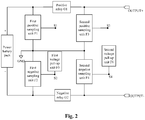
- Fig. 2 is a schematic diagram showing the structure of the battery detection circuit according to another embodiment of the present disclosure. As shown in Fig. 2, Fig. 2 differs from Fig. 1 in that, in some embodiments, the battery detection circuit may further include a first positive sampling point S1, a first negative sampling point S2, a second positive sampling point S3, a second negative sampling point S4, a first voltage pull-up unit F5, and a second voltage pull-up unit F6.
- the embodiments of the present disclosure are not limited to the description in the above embodiment and the specific units shown in Fig. 2 .
- the battery detection circuit may include only a portion of the units therein. That is, the battery detection circuit in the embodiments of the present disclosure may include a more flexible unit configuration, which will be described below in connection with specific embodiments.
- the battery detection circuit may further include the first positive sampling point, the first negative sampling point, the second positive sampling point, and the second negative sampling point.
- the first positive sampling unit may be further configured to provide the first positive sampled signal to the first positive sampling point; the first negative sampling unit may be further configured to provide the first negative sampled signal to the first negative sampling point; the second positive sampling unit may be further configured to provide the second positive sampled signal to the second positive sampling point; and the second negative sampling unit may be further configured to provide the second negative sampled signal to the second negative sampling point.
- a terminal of the first positive sampling unit F1 may be connected to the first terminal of the positive relay G1 and the positive electrode of the battery pack to be detected; and the other terminal of the first positive sampling unit F1 may be connected to the first positive sampling point S1 and the reference voltage terminal GND.
- a terminal of the first negative sampling unit F2 may be connected to the first terminal of the negative relay G2 and the negative electrode of the battery pack to be detected; and the other terminal of the first negative sampling unit F2 may be connected to the first negative sampling point S2 and the reference voltage terminal GND.
- a terminal of the second positive sampling unit F3 may be connected to the second terminal of the positive relay G1; and the other terminal of the second positive sampling unit F3 may be connected to the second positive sampling point S3 and the reference voltage terminal GND.
- a terminal of the second negative sampling unit F4 may be connected to the second terminal of the negative relay G2; and the other terminal of the second negative sampling unit F4 may be connected to the second negative sampling point S4 and the reference voltage terminal GND.
- an actual voltage at the reference voltage terminal GND may be set in accordance with working scene and demand of a high voltage sampling circuit.
- the voltage at the reference voltage terminal GND can be regarded as the reference voltage of the battery detection circuit in the embodiment.
- the reference voltage at the reference voltage terminal GND can be regarded as relative 0V.
- the reference voltage 6V can be recorded as 0V
- the voltage of the sampled signal acquired at the first positive sampling point S1 can be recorded as 16V.
- all of a sampled voltage U SP1 of the first positive sampled signal at the first positive sampling point S1, a sampled voltage U SP2 of the first negative sampled signal at the first negative sampling point S2, a sampled voltage U SP3 of the second positive sampled signal at the second positive sampling point S3 and a sampled voltage U SP4 of the second negative sampled signal at the second negative sampling point S4 may share a same reference voltage.
- the reference voltage terminal may be a low voltage ground.
- all of the first positive sampling unit F1, the first negative sampling unit F2, the second positive sampling unit F3, the second negative sampling unit F4 and the power battery pack to be detected may be connected to the common low voltage ground.
- the voltages may be detected by the first positive sampling unit F1, the first negative sampling unit F2, the second positive sampling unit F3 and the second negative sampling unit F4.
- these sampling units employ the same reference voltage (e.g. they are connected to the common low voltage ground)
- both the sampled voltage U SP2 of the first negative sampled signal at the first negative sampling point S2 and the sampled voltage U SP4 of the second negative sampled signal at the second negative sampling point S4 may be lower than the voltage (i.e. relative 0V) at the reference voltage terminal GND because of the voltage drop of the current.
- both the sampled voltage U SP2 and the sampled voltage U SP4 may be recorded as a negative voltage.
- the battery detection circuit may further include the first voltage pull-up unit F5 and the second voltage pull-up unit F6.
- the first voltage pull-up unit F5 may be connected to the first negative sampling point S2, and the first voltage pull-up unit F5 may be configured to pull up the first negative sampled signal to be a positive voltage signal.
- the second voltage pull-up unit F6 may be connected to the second negative sampling point S4, and the second voltage pull-up unit F6 may be configured to pull up the second negative sampled signal to be a positive voltage signal.
- the voltage of the first negative sampled signal at the first negative sampling point S2 and the voltage of the second negative sampled signal at the second negative sampling point S4 are pulled up by a preset pull-up voltage value, so that both the output voltage U SP2 of the first negative sampled signal at the first negative sampling point S2 and the output voltage U SP4 of the second negative sampled signal at the second negative sampling point S4 may be higher than the voltage at the reference voltage terminal. That is, after the voltage pull-up process, both the voltage U SP2 of the first negative sampled signal at the first negative sampling point S2 and the voltage U SP4 of the second negative sampled signal at the second negative sampling point S4 may be recorded as a positive voltage.
- the battery detection circuit may implement voltage sampling for a high voltage circuit, insulation detection for the power battery pack to be detected and relay diagnosis for the battery detection circuit, based on the first positive sampled signal acquired from the first positive sampling point S1, the first negative sampled signal acquired from the first negative sampling point S2, the second positive sampled signal acquired from the second positive sampling point S3 and the second negative sampled signal acquired from the second negative sampling point S4.
- Fig. 3 is a schematic diagram showing a structure of a battery detection circuit according to an exemplary embodiment of the present disclosure.
- Fig. 3 schematically shows specific structures of the first positive sampling unit F1, the first negative sampling unit F2, the second positive sampling unit F3, the second negative sampling unit F4, the first voltage pull-up unit F5, and the second voltage pull-up unit F6.
- the first positive sampling unit F1 may include a first resistor network R1 and a second resistor network R2 in series.
- a terminal of the first resistor network R1 may be connected to the first terminal of the positive relay G1 and the positive electrode of the battery pack to be detected, and the other terminal of the first resistor network R1 may be connected to the first positive sampling point S1 and a terminal of the second resistor network R2.
- the other terminal of the second resistor network R2 may be connected to the reference voltage terminal GND.
- the resistor network form and the resistance value of the first resistor network R1 may be the same as the resistor network form and the resistance value of the second resistor network R2.
- the first resistor network R1 and the second resistor network R2 may function as a divider.
- the range of the first positive sampled signal at the first positive sampling point S1 can be adjusted by adjusting the resistance value of the first resistor network R1 and the resistance value of the second resistor network R2.
- the first negative sampling unit F2 may include a third resistor network R3 and a fourth resistor network R4 in series.
- a terminal of the third resistor network R3 may be connected to the reference voltage terminal GND, and the other terminal of the third resistor network R3 may be connected to the first negative sampling point S2 and a terminal of the fourth resistor network R4.
- the other terminal of the fourth resistor network R4 may be connected to the first terminal of the negative relay G2 and the negative electrode of the battery pack to be detected.
- the resistor network form and the resistance value of the third resistor network R3 may be the same as the resistor network form and the resistance value of the fourth resistor network R4.
- the third resistor network R3 and the fourth resistor network R4 may function as a divider.
- the range of the first negative sampled signal at the first negative sampling point S2 can be adjusted by adjusting the resistance value of the third resistor network R3 and the resistance value of the fourth resistor network R4.
- the second positive sampling unit F3 may include a fifth resistor network R5 and a sixth resistor network R6 in series.
- a terminal of the fifth resistor network R5 may be connected to the second terminal of the positive relay G1, and the other terminal of the fifth resistor network R5 may be connected to the second positive sampling point S3 and a terminal of the sixth resistor network R6.
- the other terminal of the sixth resistor network R6 may be connected to the reference voltage terminal GND.
- the resistor network form and the resistance value of the fifth resistor network R5 may be the same as the resistor network form and the resistance value of the sixth resistor network R6.
- the fifth resistor network R5 and the sixth resistor network R6 may function as a divider.
- the range of the second positive sampled signal at the second positive sampling point S3 can be adjusted by adjusting the resistance value of the fifth resistor network R5 and the resistance value of the sixth resistor network R6.
- the second negative sampling unit F4 may include a seventh resistor network R7 and an eighth resistor network R8 in series.
- a terminal of the seventh resistor network R7 may be connected to the reference voltage terminal GND, and the other terminal of the seventh resistor network R7 may be connected to the second negative sampling point S4 and a terminal of the eighth resistor network R8.
- the other terminal of the eighth resistor network R8 may be connected to the second terminal of the negative relay G2.
- the resistor network form and the resistance value of the seventh resistor network R7 may be the same as the resistor network form and the resistance value of the eighth resistor network R8.
- the seventh resistor network R7 and the eighth resistor network R8 may function as a divider.
- the range of the second negative sampled signal at the second negative sampling point S4 can be adjusted by adjusting the resistance value of the seventh resistor network R7 and the resistance value of the eighth resistor network R8.
- the first voltage pull-up unit F5 may further include a first DC (Direct Current) voltage source DV1 and a ninth resistor network R9.
- a terminal of the ninth resistor network R9 may be connected to the first negative sampling point S2, and the other terminal of the ninth resistor network R9 may be connected to the first DC voltage source DV1.
- the first DC voltage source DV1 may generate a pull-up voltage U1.
- U1 may be a preset value and U1 may be greater than the voltage at the reference voltage terminal GND.
- the second voltage pull-up unit F6 may further include a second DC voltage source DV2 and a tenth resistor network R10.
- a terminal of the tenth resistor network R10 may be connected to the second negative sampling point S4, and the other terminal of the tenth resistor network R10 may be connected to the second DC voltage source DV2.
- the second DC voltage source DV2 may generate a pull-up voltage U2.
- U2 may be a preset value and U2 may be greater than the voltage at the reference voltage terminal GND.
- the pull-up voltage U1 and the pull-up voltage U2 can be set to have a same pull-up voltage value.
- each of the first resistor network R1 to the tenth resistor network R10 may include a single resistor. In some other embodiments, each of the first resistor network R1 to the tenth resistor network R10 may include two or more resistors in series and/or in parallel.
- resistor network form and the resistance value of each of the first resistor network R1 to the tenth resistor network R10 may be set in the actual application scenario of the battery detection according to the actual situation.
- the resistor network form and the resistance value of each of the first resistor network R1 to the tenth resistor network R10 may be determined based on the demanded sampling accuracy and sampling range for the high voltage sampling process conducted by the battery detection circuit, the sampling range limit and the achievable sampling accuracy of the sampling units in the above described embodiments of the battery detection circuit, the tolerance range of operating voltage of components in the battery detection circuit, and the like.
- the first positive sampling unit F1 may further include a first switch K1.
- a terminal of the first resistor network R1 may be connected, via the first switch K1, to the positive electrode of the power battery pack to be detected.
- the first positive sampling point S1 provides the first positive sampled signal or not, by turning on or turning off the first switch K1.
- the first positive sampling point S1 may provide the first positive sampled signal.
- the first switch K1 is turned off, the first positive sampling point S1 may stop providing the first positive sampled signal.
- the first negative sampling unit F2 may further include a second switch K2.
- a terminal of the third resistor network R3 may be connected to the reference voltage terminal GND via the second switch K2.
- the first negative sampling point S2 provides the first negative sampled signal or not, by turning on or turning off the second switch K2.
- the first negative sampling point S2 may provide the first negative sampled signal.
- the second switch K2 is turned off, the first negative sampling point S2 may stop providing the first negative sampled signal.
- the second positive sampling unit F3 may further include a third switch K3.
- a terminal of the fifth resistor network R5 may be connected to the second terminal of the positive relay G1 via the third switch K3.
- the second positive sampling point S3 provides the second positive sampled signal or not, by turning on or turning off the third switch K3.
- the third switch K3 When the third switch K3 is turned on, the second positive sampling point S3 may provide the second positive sampled signal.
- the third switch K3 When the third switch K3 is turned off, the second positive sampling point S3 may stop providing the second positive sampled signal.
- the second negative sampling unit F4 may further include a fourth switch K4.
- a terminal of the seventh resistor network R7 may be connected to the reference voltage terminal GND via the fourth switch K4.
- the second negative sampling point S4 provides the second negative sampled signal or not, by turning on or turning off the fourth switch K4.
- the fourth switch K4 When the fourth switch K4 is turned on, the second negative sampling point S4 may provide the second negative sampled signal.
- the fourth switch K4 When the fourth switch K4 is turned off, the second negative sampling point S4 may stop providing the second negative sampled signal.
- each of the first positive sampling point S1, the first negative sampling point S2, the second positive sampling point S3 and the second negative sampling point S4 may be connected to a sampling unit for implementing the sampling process.
- the sampling unit may be an Analog to Digital Converter (ADC).
- the ADC 1 may be connected to the first positive sampling point S1 via a sampling line SP1 to acquire the voltage on the second resistor network through the first positive sampled signal supplied from the first positive sampling point S1.
- the ADC 2 may be connected to the first negative sampling point S2 via a sampling line SP2 to acquire the voltage on the third resistor network through the first negative sampled signal supplied from the first negative sampling point S2.
- the ADC 3 may be connected to the second positive sampling point S3 via a sampling line SP3 to acquire the voltage on the sixth resistor network through the second positive sampled signal supplied from the second positive sampling point S3.
- the ADC 4 may be connected to the second negative sampling point S4 via a sampling line SP4 to acquire the voltage on the seventh resistor network through the second negative sampled signal supplied from the second negative sampling point S4.
- the battery detection circuit according to the embodiment of the present disclosure may provide an integral circuitry to implement the high voltage sampling, the insulation detection and the relay diagnosis. With such a battery detection circuit, it is possible to acquire the voltage of the battery pack, detect an insulation resistance value of the battery pack and diagnose whether the relay has failed.
- the structure of the circuit may be simplified and the cost of the circuit may be reduced.
- the battery to be detected and each of the first positive sampling unit F1, the first negative sampling unit F2, the second positive sampling unit F3 and the second negative sampling unit F4 may be connected to a common ground.
- the isolation unit for isolating the sampled signal thereby simplifying the circuit structure, reducing the error caused by isolating the sampled signal, and thus improving the accuracy of the voltage of the sampled signal.
- Fig. 4 is a schematic diagram showing a structure of the battery detection circuit according to the further embodiment of the present disclosure.
- a same reference number may indicate a same element.
- the battery detection circuit shown in Fig. 4 is almost the same as the battery detection circuit shown in Fig. 2 and only has the following differences.
- the first negative sampling unit F2 and the second negative sampling unit F4 may be connected to the voltage pull-up unit F7.
- the voltage pull-up unit F7 may pull up the sampled voltage of the first negative sampled signal and the sample voltage of the second negative sampled signal to be a positive voltage signal.
- the battery detection circuit may further include a first fixed resistor network R net1 .
- a first terminal of the first fixed resistor network R net1 may be connected to the positive electrode of the power battery pack to be detected.
- a second terminal of the first fixed resistor network R net1 may be connected to the reference voltage terminal GND.
- the battery management system may further include a second fixed resistor network R net2 .
- a first terminal of the second fixed resistor network R net2 may be connected to the negative electrode of the power battery pack to be detected.
- a second terminal of the second fixed resistor network R net2 may be connected to the reference voltage terminal GND.
- the battery management system may include both the first fixed resistor network R net1 and the second fixed resistor network R net2 .
- Fig. 4 also schematically shows positions of a positive insulation resistance and a negative insulation resistance of the power battery pack to be detected in the circuit diagram of the battery detection circuit.
- R p indicates the positive insulation resistance of the power battery pack
- R n indicates the negative insulation resistance of the power battery pack.
- a terminal of R p may be connected to the positive electrode of the power battery pack to be detected, and the other terminal of R p may be connected to the reference voltage terminal GND; a terminal of R n may be connected to the reference voltage terminal GND, and the other terminal of R n may be connected to the negative electrode of the power battery pack to be detected.
- Fig. 5 is a circuit diagram of the battery detection circuit according to the further exemplary embodiment of the present disclosure.
- Fig. 5 schematically shows specific structures of the first positive sampling unit F1, the first negative sampling unit F2, the second positive sampling unit F3, the second negative sampling unit F4, the voltage pull-up unit F7, the first fixed resistor network R net1 and the second fixed resistor network R net2 .
- the voltage pull-up unit may include a DC voltage source DV, the ninth resistor network R9 and the tenth resistor network R10.
- a terminal of the ninth resistor network R9 may be connected to the first negative sampling point S2, and the other terminal of the ninth resistor network R9 may be connected to the DC voltage source DV.
- the DC voltage source DV and the ninth resistor network R9 may generate the pull-up voltage U1.
- U1 may be a preset value and U1 may be greater than the voltage at the reference voltage terminal GND.
- a terminal of the tenth resistor network R10 may be connected to the second negative sampling point S4, and the other terminal of the tenth resistor network R10 may be connected to the DC voltage source DV.
- the DC voltage source DV and the tenth resistor network R10 may generate the pull-up voltage U2.
- U2 may be a preset value and U2 may be greater than the voltage at the reference voltage terminal GND.
- the pull-up voltage U1 and the pull-up voltage U2 can be set to have a same pull-up voltage value.
- each of the sampled voltage of the first negative sampled signal and the sampled voltage of the second negative sampled signal may be pulled up to be a positive voltage signal via the voltage pull-up unit F7 according to the embodiments of the present disclosure.
- each of the first fixed resistor network R net1 and the second fixed resistor network R net2 may include a single resistor. In some other embodiments, each of the first fixed resistor network R net1 and the second fixed resistor network R net2 may include two or more resistors in series and/or in parallel.
- the resistor network form and the resistance value of the first fixed resistor network R net1 may be the same as the resistor network form and the resistance value of the second fixed resistor network R net2 .
- Fig. 5 also schematically shows positions of the positive insulation resistance and the negative insulation resistance of the power battery pack to be detected in the circuit diagram of the battery detection circuit.
- R p indicates the positive insulation resistance of the power battery pack
- R n indicates the negative insulation resistance of the power battery pack.
- a terminal of the positive insulation resistance R p may be connected to the positive electrode of the power battery pack to be detected, and the other terminal of R p may be connected to the reference voltage terminal GND; a terminal of the negative insulation resistance R n may be connected to the reference voltage terminal GND, and the other terminal of R n may be connected to the negative electrode of the power battery pack to be detected.
- a battery management system according to an embodiment of the present disclosure will be described in detail below.
- Fig. 6 is a schematic diagram showing a structure of the battery management system in an embodiment.
- the battery management system may include the battery detection circuit in the above embodiments and a processor C1 that is connected to the battery detection circuit.
- Fig. 6 also schematically shows positions of the positive insulation resistance and the negative insulation resistance of the power battery pack to be detected in the circuit diagram of the battery detection circuit.
- a terminal of R p may be connected to the positive electrode of the power battery pack to be detected, and the other terminal of R p may be connected to the reference voltage terminal GND; a terminal of R n may be connected to the reference voltage terminal GND, and the other terminal of R n may be connected to the negative electrode of the power battery pack to be detected.
- the processor C1 in the battery management system may be directly connected to the first positive sampling point S1, the first negative sampling point S2, the second positive sampling point S3, and the second negative sampling point S4.
- the processor C1 may have the function of converting each of the first positive sampled signal, the first negative sampled signal, the second positive sampled signal, and the second negative sampled signal to a digital signal.
- the battery management system may further include an ADC1.
- a terminal of the ADC1 may be connected to the first positive sampling point S1, and the other terminal of the ADC1 may be connected to the processor C1.
- the ADC1 may be configured to convert the first positive sampled signal into a digital signal.
- the battery management system may further include an ADC2.
- a terminal of the ADC2 may be connected to the first negative sampling point S2, and the other terminal of the ADC2 may be connected to the processor C1.
- the ADC2 may be configured to convert the first negative sampled signal into a digital signal.
- the battery management system may further include an ADC3.
- a terminal of the ADC3 may be connected to the second positive sampling point S3, and the other terminal of the ADC3 may be connected to the processor C1.
- the ADC3 may be configured to convert the second positive sampled signal into a digital signal.
- the battery management system may further include an ADC4.
- a terminal of the ADC4 may be connected to the second negative sampling point S4, and the other terminal of the ADC4 may be connected to the processor C1.
- the ADC4 may be configured to convert the second negative sampled signal into a digital signal.
- the ADC1, the ADC2, the ADC3 and the ADC4 may be connected to the processor C1, so that the processor C1 may operate according to each of the digital signal of the positive sampled signal, the digital signal of the first negative sampled signal, the digital signal of the second positive sampled signal, and the digital signal of the second negative sampled signal.
- the battery management system may implement the high voltage sampling process for the power battery pack, detect the insulation resistance value of the power battery pack and diagnose whether the relay has failed.
- the voltage between the first terminal of the positive relay G1 and the first terminal of the negative relay G2 may be referred to as a relay-input voltage of the power battery pack to be detected, and the voltage between the second terminal of the positive relay G1 and the second terminal of the negative relay G2 may be referred to as a relay-output voltage of the power battery pack to be detected.
- the processor C1 may calculate the relay-input voltage and the relay-output voltage of the power battery pack to be detected, based on the first positive sampled signal, the first negative sampled signal, the second positive sampled signal, and the second negative sampled signal.
- the high voltage sampling may be implemented as follows.
- the first positive sampling point S1 may provide the first positive sampled signal; the first negative sampling point S2 may provide the first negative sampled signal; the second positive sampling point S3 may stop providing the second positive sampled signal; and the second negative sampling point S4 may stop providing the second negative sampled signal.
- the processor C1 may calculate the voltage at the first terminal of the positive relay G1 based on the first positive sampled signal, which is the voltage of the power battery pack at the first terminal of the positive relay G1.
- the voltage may also be referred to as a positive-terminal-relay-input voltage of the power battery pack.
- the processor C1 may calculate the voltage at the first terminal of the negative relay G2 based on the first negative sampled signal, which is the voltage of the power battery pack at the first terminal of the negative relay G2.
- the voltage may also be referred to as a negative-terminal-relay-input voltage of the power battery pack.
- the processor C1 may calculate the relay-input voltage of the power battery pack, based on the voltage at the first terminal of the positive relay G1 and the voltage at the first terminal of the negative relay G2.
- the processor C1 may calculate the relay-input voltage of the power battery pack, based on the positive-terminal-relay-input voltage and the negative-terminal-relay-input voltage of the power battery pack.
- the sampled voltage U sp1 of the first positive sampled signal may be obtained from the first positive sampled signal supplied from the first positive sampling point S1. Based on the sampled voltage U sp1 of the first positive sampled signal, the first resistor network R1 and the second resistor network R2 in series, the voltage of the power battery pack at the first terminal of the positive relay G1 (i.e. the positive-terminal-relay-input voltage of the power battery pack) may be calculated according to the Ohm's Law.
- the sampled voltage U sp2 of the first negative sampled signal may be obtained from the first negative sampled signal supplied from the first negative sampling point S2.
- the third resistor network R3 and the fourth resistor network R4 in series the voltage of the power battery pack at the first terminal of the negative relay G2 (i.e. the negative-terminal-relay-input voltage of the power battery pack) may be calculated according to the Ohm's Law.
- the relay-input voltage of the power battery pack may be obtained by calculating a sum of the positive-terminal-relay-input voltage of the power battery pack and the negative-terminal-relay-input voltage of the power battery pack.
- the high voltage sampling may be implemented as follows.
- the first positive sampling point S1 may stop providing the first positive sampled signal; the first negative sampling point S2 may stop providing the first negative sampled signal; the second positive sampling point S3 may provide the second positive sampled signal; and the second negative sampling point S4 may provide the second negative sampled signal.
- the processor C1 may calculate the voltage at the second terminal of the positive relay G1 based on the second positive sampled signal, which is the voltage of the power battery pack at the second terminal of the positive relay G1.
- the voltage may also be referred to as a positive-terminal-relay-output voltage of the power battery pack.
- the processor C1 may calculate the voltage at the second terminal of the negative relay G2 based on the second negative sampled signal, which is the voltage of the power battery pack at the second terminal of the negative relay G2.
- the voltage may also be referred to as a negative-terminal-relay-output voltage of the power battery pack.
- the processor C1 may calculate the relay-output voltage of the power battery pack, based on the voltage at the second terminal of the positive relay G1 and the voltage at the second terminal of the negative relay G2.
- the processor C1 may calculate the relay-output voltage of the power battery pack, based on the positive-terminal-relay-output voltage and the negative-terminal-relay-output voltage of the power battery pack.
- the sampled voltage U sp3 of the second positive sampled signal may be obtained from the second positive sampled signal supplied from the second positive sampling point S3.
- the voltage of the power battery pack at the second terminal of the positive relay G1 i.e. the positive-terminal-relay-output voltage of the power battery pack
- the Ohm's Law the Ohm's Law
- the sampled voltage U sp4 of the second negative sampled signal may be obtained from the second negative sampled signal supplied from the second negative sampling point S4.
- the seventh resistor network R7 and the eighth resistor network R8 in series the voltage of the power battery pack at the second terminal of the negative relay G2 (i.e. the negative-terminal-relay-output voltage of the power battery pack) may be calculated according to the Ohm's Law.
- the relay-output voltage of the power battery pack may be obtained by calculating a sum of the positive-terminal-relay-output voltage of the power battery pack and the negative-terminal-relay-output voltage of the power battery pack.
- the battery detection circuit of the embodiment may be utilized to calculate the relay-input voltage and the relay-output voltage of the power battery pack based on the sampled voltage U sp1 , the sampled voltage U sp2 , the sampled voltage U sp3 , and the sampled voltage U sp4 , so as to implement the high voltage sampling.
- an absolute value of a difference between the voltage at the first terminal of the positive relay G1 and the voltage of the second terminal of the positive relay G1 may be compared with a voltage threshold of the positive relay G1, to obtain a comparison result for determining an operating state of the positive relay G1.
- the voltage at the first terminal of the positive relay G1 i.e. the positive-terminal-relay-input voltage U B+ (input) of the power battery pack
- the voltage at the second terminal of the positive relay G1 i.e. the positive-terminal-relay-output voltage U B+ (output) of the power battery pack
- U relay+ is a preset voltage drop of the relay coil at a positive terminal of the power battery pack to be detected.
- the positive relay G1 when the positive relay G1 is controlled to be turned on, if the absolute value of the difference between the voltage at the first terminal of the positive relay G1 and the voltage of the second terminal of the positive relay G1 is smaller than or equals to the preset voltage drop of the relay coil at the positive terminal of the power battery pack, it may be determined that the positive relay G1 is in the normal operating state.
- an absolute value of a difference between the voltage at the first terminal of the negative relay G2 and the voltage of the second terminal of the negative relay G2 may be compared with a voltage threshold of the negative relay G2, to obtain a comparison result for determining an operating state of the negative relay G2.
- the voltage at the first terminal of the negative relay G2 i.e. the negative-terminal-relay-input voltage U B- (input) of the power battery pack
- the voltage at the second terminal of the negative relay G2 i.e. the negative-terminal-relay-output voltage U B- (output) of the power battery pack
- U relay- is a preset voltage drop of the relay coil at a negative terminal of the power battery pack to be detected.
- the operating state of the relay coil at the positive terminal of the power battery pack can be diagnosed according to the positive-terminal-relay-input voltage and the positive-terminal-relay-output voltage of the power battery pack obtained in the high voltage sampling process and the preset voltage drop of the relay coil at the positive terminal of the power battery pack; and the operating state of the relay coil at the negative terminal of the power battery pack can be diagnosed according to the negative-terminal-relay-input voltage and the negative-terminal-relay-output voltage of the power battery pack obtained in the high voltage sampling process and the preset voltage drop of the relay coil at the negative terminal of the power battery pack.
- the battery management system may include the battery detection circuit in the above embodiments and the processor C1 that is connected to the battery detection circuit.
- Fig. 7 also schematically shows the positions of the positive insulation resistance and the negative insulation resistance of the power battery pack to be detected in the circuit diagram of the battery detection circuit.
- R p indicates the positive insulation resistance of the power battery pack
- R n indicates the negative insulation resistance of the power battery pack.
- a terminal of R p may be connected to the positive electrode of the power battery pack to be detected, and the other terminal of R p may be connected to the reference voltage terminal GND; a terminal of R n may be connected to the reference voltage terminal GND, and the other terminal of R n may be connected to the negative electrode of the power battery pack to be detected.
- the processor C1 may simultaneously turn on the first switch K1 and the second switch K2.
- the state of the switches may be referred to as a first switch state.
- a positive terminal voltage U p0 and a negative terminal voltage U n0 of the power battery pack under the first switch state may be calculated based on the first positive sampled signal acquired from the first positive sampling point S1 and the first negative sampled signal acquired from the first negative sampling point S2 under the first switch state.
- the processor C1 may turn on the first switch K1 and turn off the second switch K2.
- the state of the switches may be referred to as a second switch state.
- a positive terminal voltage U p1 of the power battery pack under the second switch state may be calculated based on the first positive sampled signal acquired under the second switch state.
- the processor C1 may turn off the first switch K1 and turn on the second switch K2.
- the state of the switches may be referred to as a third switch state.
- a negative terminal voltage U n2 of the power battery pack under the third switch state may be calculated based on the first negative sampled signal acquired under the third switch state.
- the processor C1 may calculate the positive insulation resistance value and the negative insulation resistance value of the power battery pack, based on the positive terminal voltage U p0 of the power battery pack under the first switch state, the negative terminal voltage U n0 of the power battery pack under the first switch state, the positive terminal voltage U p1 of the power battery pack under the second switch state, and the negative terminal voltage U n2 of the power battery pack under the third switch state.
- the processor C1 may obtain the following Formula (5) based on the sampled voltage U mp0 of the first positive sampled signal and the sampled voltage U mn0 of the first negative sampled signal acquired under the first switch state.
- U p 0 U mp 0
- R 1 + R 2 R 2 U n 0 U mn 0
- U p0 indicates the positive terminal voltage of the power battery pack under the first switch state
- U n0 indicates the negative terminal voltage of the power battery pack under the first switch state
- R 1 indicates the resistance value of the first resistor network
- R 2 indicates the resistance value of the second resistor network
- R 3 indicates the resistance value of the third resistor network
- R 4 indicates the resistance value of the fourth resistor network
- R p indicates the positive insulation resistance value of the power battery pack
- R n indicates the negative insulation resistance value of the power battery pack.
- the processor C1 may obtain the following Formula (6) based on the sampled voltage U mp1 of the first positive sampled signal acquired under the second switch state.
- U p 1 U mp 1 R 1 + R 2 R 2
- U n 1 U B
- U p 1 + R 2 R 1 + R 2 + R p R n U B U n 1 + U p 1
- U p1 indicates the positive terminal voltage of the power battery pack under the second switch state
- U n1 indicates the negative terminal voltage of the power battery pack under the second switch state
- R 1 indicates the resistance value of the first resistor network
- R 2 indicates the resistance value of the second resistor network
- R p indicates the positive insulation resistance value of the power battery pack
- R n indicates the negative insulation resistance value of the power battery pack.
- the processor C1 may obtain the following Formula (7) based on the sampled voltage U mn2 of the first negative sampled signal acquired under the third switch state.
- U n 2 U mn 2 R 3 + R 4 R 3
- U p2 indicates the positive terminal voltage of the power battery pack under the third switch state
- U n2 indicates the negative terminal voltage of the power battery pack under the third switch state
- R 3 indicates the resistance value of the third resistor network
- R 4 indicates the resistance value of the fourth resistor network
- R p indicates the positive insulation resistance value of the power battery pack
- R n indicates the negative insulation resistance value of the power battery pack.
- the positive insulation resistance R p and the negative insulation resistance R n of the power battery pack may be obtained by combining the Formulas (5), (6), and (7).
- R p ⁇ R a ⁇ R b ⁇ R a U mp 1 + R b U mp 1 ⁇ R b U B U mn 2
- R n ⁇ R a ⁇ R b ⁇ R a U mn 2 + R b U mn 2 ⁇ R b U B U mp 1
- Fig. 8 is a schematic diagram showing a structure of a battery management system according to another embodiment of the present disclosure
- Fig. 9 is a circuit diagram of the battery management system according to another embodiment of the present disclosure.
- the battery management system may include the battery detection circuit and the processor C1 that is connected to the battery detection circuit.
- experimental results show that when the difference between the positive insulation resistance R p and the negative insulation resistance R n is large, the sampling accuracy of the battery detection circuit is low; when the difference between the positive insulation resistance R p and the negative insulation resistance R n is small, the sampling accuracy of the battery detection circuit is high.
- the battery detection circuit may include at least one of the first fixed resistor network R net1 and the second fixed resistor network R net2 .
- the processor C1 may obtain the following Formula (9) based on the sampled voltage U mp0 of the first positive sampled signal and the sampled voltage U nm0 of the first negative sampled signal acquired under the first switch state.
- U p0 indicates the positive terminal voltage of the power battery pack under the first switch state
- U n0 indicates the negative terminal voltage of the power battery pack under the first switch state
- R 1 indicates the resistance value of the first resistor network
- R 2 indicates the resistance value of the second resistor network
- R 3 indicates the resistance value of the third resistor network
- R 4 indicates the resistance value of the fourth resistor network
- R p indicates the positive insulation resistance value of the power battery pack
- R n indicates the negative insulation resistance value of the power battery pack
- R net1 indicates the resistance value of the first fixed resistor network
- R net2 indicates the resistance value of the second fixed resistor network
- R p / / R net 1 indicates the parallel resistance value of the positive insulation resistance and the first fixed resistor network
- R n / / R net2 indicates the parallel resistance value of the negative insulation resistance and the second fixed resistor network.
- the processor C1 may obtain the following Formula (10) based on the sampled voltage U mp1 of the first positive sampled signal acquired under the second switch state.
- U p 1 U mp 1 R 1 + R 2 R 2
- U n 1 U B
- U B U n 1 + U p 1
- U p1 indicates the positive terminal voltage of the power battery pack under the second switch state
- U n1 indicates the negative terminal voltage of the power battery pack under the second switch state
- R 1 indicates the resistance value of the first resistor network
- R 2 indicates the resistance value of the second resistor network
- R p indicates the positive insulation resistance value of the power battery pack
- R n indicates the negative insulation resistance value of the power battery pack
- R p / / R net 1 indicates the parallel resistance value of the positive insulation resistance and the first fixed resistor network
- R n / / R net2 indicates the parallel resistance value of the negative insulation resistance and the second fixed resistor network.
- the processor C1 may obtain the following Formula (11) based on the sampled voltage U mn2 of the first negative sampled signal acquired under the third switch state.
- U n 2 U mn 2 R 3 + R 4 R 3
- U p 2 U B ⁇ U n 2 U n 2
- U p 2 R n / / R net 2 R 3 + R 4 R 3 + R 4 + R n / / R net 2 R n / / R net 2
- U B U n 2 + U p 2
- U p2 indicates the positive terminal voltage of the power battery pack under the third switch state
- U n2 indicates the negative terminal voltage of the power battery pack under the third switch state
- R 3 indicates the resistance value of the third resistor network
- R 4 indicates the resistance value of the fourth resistor network
- R p indicates the positive insulation resistance value of the power battery pack
- R n indicates the negative insulation resistance value of the power battery pack
- R p / / R net 1 indicates the parallel resistance value of the positive insulation resistance and the first fixed resistor network
- R n / / R net2 indicates the parallel resistance value of the negative insulation resistance and the second fixed resistor network.
- the positive insulation resistance R p and the negative insulation resistance R n of the power battery pack may be obtained by combining the Formulas (9), (10), and (11).
- the sampling accuracy of the battery detection circuit may be improved by adding the fixed resistor network R net1 and the fixed resistor network R net2 as described above. Also, due to the low price of resistors, the cost-performance ratio of the battery detection circuit can be improved by reducing the cost.
- an integral design for implementing the high voltage sampling, the insulation detection, and the relay diagnosis for the power battery pack to be detected may be conceived.
- the issues such as complex structure, high cost and low accuracy caused by separately implementing the high voltage sampling, the insulation detection and the relay diagnosis can be solved.
- the circuit structure can be simplified, the circuit cost can be reduced and the accurate sampling and detection results can be obtained.
Abstract
Description
- The present disclosure relates to the field of batteries, and more particularly to a battery detection circuit and a battery management system.
- In view of the energy saving and the environmental protection provided by electric vehicles, it has become a trend of the automotive industry to use the electric vehicles instead of fuel vehicles. As a core component of an electric vehicle, an on-board battery pack is a power guarantee for a normal driving of the electric vehicle. In order to reduce the risk at the time of energy supply by the on-board battery pack, it is needed to design a special battery diagnosis circuit for detecting battery safety issues such as safety issues of the battery pack under high voltages, and specify a corresponding management strategy to deal with the safety issues under high voltages and thus ensure the safety performance of the on-board battery pack in the electric vehicle.
- At present, in a battery detection circuit, the power battery pack and a sampling unit are usually set to not be connected to a common ground. Specifically, it means that positive and negative electrodes of the power battery pack are grounded at a high voltage, while the sampling unit is grounded at a low voltage. In order to isolate a high voltage ground signal of the power battery pack from interfering with a sampled signal of the sampling unit, an insolation unit may be additionally disposed behind the sampling unit.
- However, the existing insolation unit may further introduce a new interference signal while isolating the high voltage ground signal of the power battery pack, resulting in a decrease in the accuracy of the sampled signal.
- The present disclosure provides a battery detection circuit and a battery management system, so that both the cost of the battery detection circuit and the complexity of the structure of the battery detection circuit can be reduced.
- According to an aspect of embodiments of the present disclosure, a battery detection circuit is provided. The battery detection circuit may include a positive relay, a negative relay, a first positive sampling unit, a first negative sampling unit, a second positive sampling unit, a second negative sampling unit, and a reference voltage terminal, wherein: a first terminal of the positive relay is connected to a positive electrode of a power battery pack to be detected, a first terminal of the negative relay is connected to a negative electrode of the power battery pack to be detected, and each of the first positive sampling unit, the first negative sampling unit, the second positive sampling unit, and the second negative sampling unit is connected to the reference voltage terminal; the first positive sampling unit is configured to acquire a first positive sampled signal of the power battery pack to be detected at the first terminal of the positive relay; the first negative sampling unit is configured to acquire a first negative sampled signal of the power battery pack to be detected at the first terminal of the negative relay; the second positive sampling unit is configured to acquire a second positive sampled signal of the power battery pack to be detected at a second terminal of the positive relay; and the second negative sampling unit is configured to acquire a second negative sampled signal of the power battery pack to be detected at a second terminal of the negative relay.
- According to another aspect of embodiments of the present disclosure, a battery management system is provided. The battery management system may include the above-described battery detection circuit and a processor that is connected to the battery detection circuit. The processor may be configured to calculate a voltage at the first terminal of the positive relay based on the first positive sampled signal; calculate a voltage at the first terminal of the negative relay based on the first negative sampled signal; obtain a relay-input voltage of the power battery pack to be detected, based on the voltage at the first terminal of the positive relay and the voltage at the first terminal of the negative relay, wherein the relay-input voltage of the power battery pack to be detected is a voltage between the first terminal of the positive relay and the first terminal of the negative relay; calculate a voltage at the second terminal of the positive relay based on the second positive sampled signal; calculate a voltage at the second terminal of the negative relay based on the second negative sampled signal; and obtain a relay-output voltage of the power battery pack to be detected, based on the voltage at the second terminal of the positive relay and the voltage at the second terminal of the negative relay, wherein the relay-output voltage of the power battery pack to be detected is a voltage between the second terminal of the positive relay and the second terminal of the negative relay.
- According to the embodiments of the present disclosure, the battery detection circuit includes the positive relay, the negative relay, the first positive sampling unit, the first negative sampling unit, the second positive sampling unit and the second negative sampling unit. The power battery pack to be detected and each of the sampling units are connected to the same reference voltage terminal, so that the circuit structure can be simplified and the accuracy of the sampled signal can be improved.
- Furthermore, in the embodiments of the present disclosure, the battery management system may be integrated with an integral circuit for implementing high voltage sampling, insulation detection and relay diagnosis, and thus the battery management system may have the functions of high voltage sampling, insulation detection and relay diagnosis. Consequently, both the cost of the battery detection circuit and the complexity of the structure of the battery detection circuit can be reduced, and the processing efficiency of the battery management system may be improved.
- To more clearly illustrate technical solutions of embodiments of the present disclosure, the accompanying drawings, which are to be referred by the embodiments of the present disclosure, will be briefly described. Those skilled in the art will be able to obtain additional drawings in accordance with these drawings without any creative work.
-
Fig. 1 is a schematic diagram showing a structure of a battery detection circuit according to an embodiment of the present disclosure; -
Fig. 2 is a schematic diagram showing a structure of a battery detection circuit according to another embodiment of the present disclosure; -
Fig. 3 is a circuit diagram of a battery detection circuit according to an exemplary embodiment of the present disclosure; -
Fig. 4 is a schematic diagram showing a structure of a battery detection circuit according to a further embodiment of the present disclosure; -
Fig. 5 is a circuit diagram of a battery detection circuit according to a further exemplary embodiment of the present disclosure; -
Fig. 6 is a schematic diagram showing a structure of a battery management system according to an embodiment of the present disclosure; -
Fig. 7 is a circuit diagram of a battery management system according to an embodiment of the present disclosure; -
Fig. 8 is a schematic diagram showing a structure of a battery management system according to another embodiment of the present disclosure; -
Fig. 9 is a circuit diagram of a battery management system according to another embodiment of the present disclosure. - Various aspects of features and exemplary embodiments of the present disclosure will be described in detail below. The present disclosure will be provided in further detail below in conjunction with accompanying drawings and embodiments in order to make objects, technical solutions and advantages of the present disclosure to be more clearly understood. It is to be appreciated that the specific embodiments described herein are to be construed to illustrate the present disclosure but not to limit the present disclosure. It will be apparent to those skilled in the art that the present disclosure may be practiced without some of these specific details. The following description of the embodiments is merely to provide a better understanding of the present disclosure by illustrating examples thereof.
- It is to be noted that relational terms such as first, second and the like are used herein only to distinguish an entity or operation from another entity or operation without requiring or implying that there is any such actual relationship or order between these entities or operations. Moreover, the term "comprise", "include" or any other variant thereof is intended to encompass a non-exclusive inclusion, such that a process, method, article or device that includes a series of elements includes not only these elements but also other elements that are not explicitly listed or those elements that are inherent to such a process, method, article or device. In the absence of more restrictions, elements defined by the statement "includes ..." do not preclude the presence of additional identical elements in the process, method, article or device that includes the elements.
- In embodiments of the present disclosure, in terms of battery type, the battery pack to be detected may be a lithium ion battery, a lithium metal battery, a lead acid battery, a nickel cadmium battery, a nickel hydrogen battery, a lithium sulfur battery, a lithium air battery, or a sodium ion, which is not particularly limited in the embodiments of the present disclosure. In terms of battery scale, the battery pack to be detected may be a cell or a battery module or a battery pack, which is not particularly limited in the embodiments of the present disclosure.
- With the battery detection circuit and the battery management system provided in the embodiments of the present disclosure, the battery management system may be integrated with an integral circuit implementing high voltage sampling, insulation detection and relay diagnosis, and thus the battery management system may have the functions of high voltage sampling, insulation detection and relay diagnosis.
- For a better understanding of the present disclosure, the battery detection circuit according to embodiments of the present disclosure will be described in detail with reference to
Figs. 1 ,2 and3 . It is to be noted that these embodiments are not intended to limit the scope of the present disclosure. -
Fig. 1 is a schematic diagram showing a structure of a battery detection circuit according to an embodiment of the present disclosure. As shown inFig. 1 , the battery detection circuit may include a positive relay G1, a negative relay G2, a first positive sampling unit F1, a first negative sampling unit F2, a second positive sampling unit F3, a second negative sampling unit F4, and a reference voltage terminal GND. - In the embodiment of the present disclosure, the positive relay may be connected to a positive electrode of a power battery pack to be detected; the negative relay may be connected to a negative electrode of the power battery pack to be detected; and each of the first positive sampling unit, the first negative sampling unit, the second positive sampling unit, and the second negative sampling unit may be connected to the reference voltage terminal.
- Further, the first positive sampling unit may be configured to acquire a first positive sampled signal of the battery pack at a first terminal of the positive relay; the first negative sampling unit may be configured to acquire a first negative sampled signal of the battery pack at a first terminal of the negative relay; the second positive sampling unit may be configured to acquire a second positive sampled signal of the battery pack at a second terminal of the positive relay; the second negative sampling unit may be configured to acquire a second negative sampled signal of the battery pack at a second terminal of the negative relay.
- In the embodiment, the sampling units and the battery pack to be detected may be connected to the same reference voltage terminal. In comparison to the case that the isolation unit needs to be additionally provided for the sampling unit when the sampling unit and the battery pack are connected to different reference voltage terminals, the structure of the circuit according to the embodiment can be simplified, and meanwhile, the new interference signal introduced by additionally providing the isolation unit can be avoided and thus the accuracy of the sampled signals can be improved.
- Referring to
Fig. 2 , a battery detection circuit according to another embodiment of the present disclosure will be described below.Fig. 2 is a schematic diagram showing the structure of the battery detection circuit according to another embodiment of the present disclosure. As shown inFig. 2, Fig. 2 differs fromFig. 1 in that, in some embodiments, the battery detection circuit may further include a first positive sampling point S1, a first negative sampling point S2, a second positive sampling point S3, a second negative sampling point S4, a first voltage pull-up unit F5, and a second voltage pull-up unit F6. - It is to be noted that the embodiments of the present disclosure are not limited to the description in the above embodiment and the specific units shown in
Fig. 2 . In some embodiments, the battery detection circuit may include only a portion of the units therein. That is, the battery detection circuit in the embodiments of the present disclosure may include a more flexible unit configuration, which will be described below in connection with specific embodiments. - In an embodiment, the battery detection circuit may further include the first positive sampling point, the first negative sampling point, the second positive sampling point, and the second negative sampling point.
- In the embodiment, the first positive sampling unit may be further configured to provide the first positive sampled signal to the first positive sampling point; the first negative sampling unit may be further configured to provide the first negative sampled signal to the first negative sampling point; the second positive sampling unit may be further configured to provide the second positive sampled signal to the second positive sampling point; and the second negative sampling unit may be further configured to provide the second negative sampled signal to the second negative sampling point.
- Continuing with reference to
Fig. 2 , in an embodiment, a terminal of the first positive sampling unit F1 may be connected to the first terminal of the positive relay G1 and the positive electrode of the battery pack to be detected; and the other terminal of the first positive sampling unit F1 may be connected to the first positive sampling point S1 and the reference voltage terminal GND. - A terminal of the first negative sampling unit F2 may be connected to the first terminal of the negative relay G2 and the negative electrode of the battery pack to be detected; and the other terminal of the first negative sampling unit F2 may be connected to the first negative sampling point S2 and the reference voltage terminal GND.
- A terminal of the second positive sampling unit F3 may be connected to the second terminal of the positive relay G1; and the other terminal of the second positive sampling unit F3 may be connected to the second positive sampling point S3 and the reference voltage terminal GND.
- A terminal of the second negative sampling unit F4 may be connected to the second terminal of the negative relay G2; and the other terminal of the second negative sampling unit F4 may be connected to the second negative sampling point S4 and the reference voltage terminal GND.
- In the embodiment, an actual voltage at the reference voltage terminal GND may be set in accordance with working scene and demand of a high voltage sampling circuit. The voltage at the reference voltage terminal GND can be regarded as the reference voltage of the battery detection circuit in the embodiment. In other words, the reference voltage at the reference voltage terminal GND can be regarded as relative 0V.
- As an example, if the actual voltage at the reference voltage terminal GND is 6V and the actual voltage of the sampled signal acquired at the first positive sampling point S1 is 22V, the reference voltage 6V can be recorded as 0V, and the voltage of the sampled signal acquired at the first positive sampling point S1 can be recorded as 16V.
- In the battery detection circuit, the other terminal of the first positive sampling unit F1 may be connected to the first positive sampling point S1 and the reference voltage terminal GND; the other terminal of the first negative sampling unit F2 may be connected to the first negative sampling point S2 and the reference voltage terminal GND; the other terminal of the second positive sampling unit F3 may be connected to the second positive sampling point S3 and the reference voltage terminal GND; and the other terminal of the second negative sampling unit F4 may be connected to the second negative sampling point S4 and the reference voltage terminal GND.
- In other words, all of a sampled voltage USP1 of the first positive sampled signal at the first positive sampling point S1, a sampled voltage USP2 of the first negative sampled signal at the first negative sampling point S2, a sampled voltage USP3 of the second positive sampled signal at the second positive sampling point S3 and a sampled voltage USP4 of the second negative sampled signal at the second negative sampling point S4 may share a same reference voltage.
- As an example, the reference voltage terminal may be a low voltage ground.
- When the reference voltage terminal GND is the low voltage ground, all of the first positive sampling unit F1, the first negative sampling unit F2, the second positive sampling unit F3, the second negative sampling unit F4 and the power battery pack to be detected may be connected to the common low voltage ground.
- In the embodiments of the present disclosure, the voltages may be detected by the first positive sampling unit F1, the first negative sampling unit F2, the second positive sampling unit F3 and the second negative sampling unit F4. When these sampling units employ the same reference voltage (e.g. they are connected to the common low voltage ground), it is possible to avoid additionally providing the isolation unit for isolating the sampled signal due to the different reference voltage terminals, thereby simplifying the circuit structure, reducing the error caused by isolating the sampled signal, and thus improving the accuracy of the voltage of the sampled signal.
- In some embodiments, when all of the above sampling units take the low voltage ground as a reference, both the sampled voltage USP2 of the first negative sampled signal at the first negative sampling point S2 and the sampled voltage USP4 of the second negative sampled signal at the second negative sampling point S4 may be lower than the voltage (i.e. relative 0V) at the reference voltage terminal GND because of the voltage drop of the current. In this case, both the sampled voltage USP2 and the sampled voltage USP4 may be recorded as a negative voltage.
- Therefore, in some embodiments, it may be necessary to apply a voltage pull-up process to the sampled voltage USP2 of the first negative sampled signal at the first negative sampling point S2 and the sampled voltage USP4 of the second negative sampled signal at the second negative sampling point S4.
- Continuing with reference to
Fig. 2 , in an embodiment, the battery detection circuit may further include the first voltage pull-up unit F5 and the second voltage pull-up unit F6. - The first voltage pull-up unit F5 may be connected to the first negative sampling point S2, and the first voltage pull-up unit F5 may be configured to pull up the first negative sampled signal to be a positive voltage signal.
- The second voltage pull-up unit F6 may be connected to the second negative sampling point S4, and the second voltage pull-up unit F6 may be configured to pull up the second negative sampled signal to be a positive voltage signal.
- In the embodiment, the voltage of the first negative sampled signal at the first negative sampling point S2 and the voltage of the second negative sampled signal at the second negative sampling point S4 are pulled up by a preset pull-up voltage value, so that both the output voltage USP2 of the first negative sampled signal at the first negative sampling point S2 and the output voltage USP4 of the second negative sampled signal at the second negative sampling point S4 may be higher than the voltage at the reference voltage terminal. That is, after the voltage pull-up process, both the voltage USP2 of the first negative sampled signal at the first negative sampling point S2 and the voltage USP4 of the second negative sampled signal at the second negative sampling point S4 may be recorded as a positive voltage.
- The battery detection circuit according to the embodiment of the present disclosure may implement voltage sampling for a high voltage circuit, insulation detection for the power battery pack to be detected and relay diagnosis for the battery detection circuit, based on the first positive sampled signal acquired from the first positive sampling point S1, the first negative sampled signal acquired from the first negative sampling point S2, the second positive sampled signal acquired from the second positive sampling point S3 and the second negative sampled signal acquired from the second negative sampling point S4.
- Next, referring to
Fig. 3 , a specific structure of the battery detection circuit according to an embodiment of the present disclosure will be described in detail with reference to specific embodiments. -
Fig. 3 is a schematic diagram showing a structure of a battery detection circuit according to an exemplary embodiment of the present disclosure.Fig. 3 schematically shows specific structures of the first positive sampling unit F1, the first negative sampling unit F2, the second positive sampling unit F3, the second negative sampling unit F4, the first voltage pull-up unit F5, and the second voltage pull-up unit F6. - As shown in
Fig. 3 , in an embodiment, the first positive sampling unit F1 may include a first resistor network R1 and a second resistor network R2 in series. - A terminal of the first resistor network R1 may be connected to the first terminal of the positive relay G1 and the positive electrode of the battery pack to be detected, and the other terminal of the first resistor network R1 may be connected to the first positive sampling point S1 and a terminal of the second resistor network R2.
- The other terminal of the second resistor network R2 may be connected to the reference voltage terminal GND.
- In an example, the resistor network form and the resistance value of the first resistor network R1 may be the same as the resistor network form and the resistance value of the second resistor network R2.
- In the embodiment, the first resistor network R1 and the second resistor network R2 may function as a divider. The range of the first positive sampled signal at the first positive sampling point S1 can be adjusted by adjusting the resistance value of the first resistor network R1 and the resistance value of the second resistor network R2.
- In an embodiment, the first negative sampling unit F2 may include a third resistor network R3 and a fourth resistor network R4 in series.
- A terminal of the third resistor network R3 may be connected to the reference voltage terminal GND, and the other terminal of the third resistor network R3 may be connected to the first negative sampling point S2 and a terminal of the fourth resistor network R4.
- The other terminal of the fourth resistor network R4 may be connected to the first terminal of the negative relay G2 and the negative electrode of the battery pack to be detected.
- In an example, the resistor network form and the resistance value of the third resistor network R3 may be the same as the resistor network form and the resistance value of the fourth resistor network R4.
- In the embodiment, the third resistor network R3 and the fourth resistor network R4 may function as a divider. The range of the first negative sampled signal at the first negative sampling point S2 can be adjusted by adjusting the resistance value of the third resistor network R3 and the resistance value of the fourth resistor network R4.
- In an embodiment, the second positive sampling unit F3 may include a fifth resistor network R5 and a sixth resistor network R6 in series.
- A terminal of the fifth resistor network R5 may be connected to the second terminal of the positive relay G1, and the other terminal of the fifth resistor network R5 may be connected to the second positive sampling point S3 and a terminal of the sixth resistor network R6.
- The other terminal of the sixth resistor network R6 may be connected to the reference voltage terminal GND.
- In some examples, the resistor network form and the resistance value of the fifth resistor network R5 may be the same as the resistor network form and the resistance value of the sixth resistor network R6.
- In the embodiment, the fifth resistor network R5 and the sixth resistor network R6 may function as a divider. The range of the second positive sampled signal at the second positive sampling point S3 can be adjusted by adjusting the resistance value of the fifth resistor network R5 and the resistance value of the sixth resistor network R6.
- In an embodiment, the second negative sampling unit F4 may include a seventh resistor network R7 and an eighth resistor network R8 in series.
- A terminal of the seventh resistor network R7 may be connected to the reference voltage terminal GND, and the other terminal of the seventh resistor network R7 may be connected to the second negative sampling point S4 and a terminal of the eighth resistor network R8.
- The other terminal of the eighth resistor network R8 may be connected to the second terminal of the negative relay G2.
- In some examples, the resistor network form and the resistance value of the seventh resistor network R7 may be the same as the resistor network form and the resistance value of the eighth resistor network R8.
- In the embodiment, the seventh resistor network R7 and the eighth resistor network R8 may function as a divider. The range of the second negative sampled signal at the second negative sampling point S4 can be adjusted by adjusting the resistance value of the seventh resistor network R7 and the resistance value of the eighth resistor network R8.
- Continuing with reference to
Fig. 3 , in an embodiment, the first voltage pull-up unit F5 may further include a first DC (Direct Current) voltage source DV1 and a ninth resistor network R9. A terminal of the ninth resistor network R9 may be connected to the first negative sampling point S2, and the other terminal of the ninth resistor network R9 may be connected to the first DC voltage source DV1. - In the embodiment, the first DC voltage source DV1 may generate a pull-up voltage U1. U1 may be a preset value and U1 may be greater than the voltage at the reference voltage terminal GND.
- In an embodiment, the second voltage pull-up unit F6 may further include a second DC voltage source DV2 and a tenth resistor network R10. A terminal of the tenth resistor network R10 may be connected to the second negative sampling point S4, and the other terminal of the tenth resistor network R10 may be connected to the second DC voltage source DV2.
- In the embodiment, the second DC voltage source DV2 may generate a pull-up voltage U2. U2 may be a preset value and U2 may be greater than the voltage at the reference voltage terminal GND.
- In an example, the pull-up voltage U1 and the pull-up voltage U2 can be set to have a same pull-up voltage value.
- In the battery detection circuit shown in
Fig. 3 , each of the first resistor network R1 to the tenth resistor network R10 may include a single resistor. In some other embodiments, each of the first resistor network R1 to the tenth resistor network R10 may include two or more resistors in series and/or in parallel. - It is to be noted that the resistor network form and the resistance value of each of the first resistor network R1 to the tenth resistor network R10 may be set in the actual application scenario of the battery detection according to the actual situation.
- As an example, the resistor network form and the resistance value of each of the first resistor network R1 to the tenth resistor network R10 may be determined based on the demanded sampling accuracy and sampling range for the high voltage sampling process conducted by the battery detection circuit, the sampling range limit and the achievable sampling accuracy of the sampling units in the above described embodiments of the battery detection circuit, the tolerance range of operating voltage of components in the battery detection circuit, and the like.
- Continuing with reference to
Fig. 3 , in some embodiments, the first positive sampling unit F1 may further include a first switch K1. A terminal of the first resistor network R1 may be connected, via the first switch K1, to the positive electrode of the power battery pack to be detected. - In the embodiments, it is possible to control whether the first positive sampling point S1 provides the first positive sampled signal or not, by turning on or turning off the first switch K1. When the first switch K1 is turned on, the first positive sampling point S1 may provide the first positive sampled signal. When the first switch K1 is turned off, the first positive sampling point S1 may stop providing the first positive sampled signal.
- In some embodiments, the first negative sampling unit F2 may further include a second switch K2. A terminal of the third resistor network R3 may be connected to the reference voltage terminal GND via the second switch K2.
- In the embodiments, it is possible to control whether the first negative sampling point S2 provides the first negative sampled signal or not, by turning on or turning off the second switch K2. When the second switch K2 is turned on, the first negative sampling point S2 may provide the first negative sampled signal. When the second switch K2 is turned off, the first negative sampling point S2 may stop providing the first negative sampled signal.
- In some embodiments, the second positive sampling unit F3 may further include a third switch K3. A terminal of the fifth resistor network R5 may be connected to the second terminal of the positive relay G1 via the third switch K3.
- In the embodiments, it is possible to control whether the second positive sampling point S3 provides the second positive sampled signal or not, by turning on or turning off the third switch K3. When the third switch K3 is turned on, the second positive sampling point S3 may provide the second positive sampled signal. When the third switch K3 is turned off, the second positive sampling point S3 may stop providing the second positive sampled signal.
- In some embodiments, the second negative sampling unit F4 may further include a fourth switch K4. A terminal of the seventh resistor network R7 may be connected to the reference voltage terminal GND via the fourth switch K4.
- In the embodiments, it is possible to control whether the second negative sampling point S4 provides the second negative sampled signal or not, by turning on or turning off the fourth switch K4. When the fourth switch K4 is turned on, the second negative sampling point S4 may provide the second negative sampled signal. When the fourth switch K4 is turned off, the second negative sampling point S4 may stop providing the second negative sampled signal.
- In some embodiments, each of the first positive sampling point S1, the first negative sampling point S2, the second positive sampling point S3 and the second negative sampling point S4 may be connected to a sampling unit for implementing the sampling process. In an example, the sampling unit may be an Analog to Digital Converter (ADC).
- As an example, the
ADC 1 may be connected to the first positive sampling point S1 via a sampling line SP1 to acquire the voltage on the second resistor network through the first positive sampled signal supplied from the first positive sampling point S1. - As an example, the
ADC 2 may be connected to the first negative sampling point S2 via a sampling line SP2 to acquire the voltage on the third resistor network through the first negative sampled signal supplied from the first negative sampling point S2. - As an example, the
ADC 3 may be connected to the second positive sampling point S3 via a sampling line SP3 to acquire the voltage on the sixth resistor network through the second positive sampled signal supplied from the second positive sampling point S3. - As an example, the
ADC 4 may be connected to the second negative sampling point S4 via a sampling line SP4 to acquire the voltage on the seventh resistor network through the second negative sampled signal supplied from the second negative sampling point S4. - The battery detection circuit according to the embodiment of the present disclosure may provide an integral circuitry to implement the high voltage sampling, the insulation detection and the relay diagnosis. With such a battery detection circuit, it is possible to acquire the voltage of the battery pack, detect an insulation resistance value of the battery pack and diagnose whether the relay has failed. The structure of the circuit may be simplified and the cost of the circuit may be reduced.
- In the battery detection circuit according to some embodiments of the present disclosure, the battery to be detected and each of the first positive sampling unit F1, the first negative sampling unit F2, the second positive sampling unit F3 and the second negative sampling unit F4 may be connected to a common ground. Thus it is not needed to additionally provide the isolation unit for isolating the sampled signal, thereby simplifying the circuit structure, reducing the error caused by isolating the sampled signal, and thus improving the accuracy of the voltage of the sampled signal.
- Referring to
Fig. 4 andFig. 5 , a battery detection circuit according to a further embodiment of the present disclosure will be described below.Fig. 4 is a schematic diagram showing a structure of the battery detection circuit according to the further embodiment of the present disclosure. In bothFig. 4 andFig. 2 , a same reference number may indicate a same element. The battery detection circuit shown inFig. 4 is almost the same as the battery detection circuit shown inFig. 2 and only has the following differences. - As shown in
Fig. 4 , in some embodiments, the first negative sampling unit F2 and the second negative sampling unit F4 may be connected to the voltage pull-up unit F7. The voltage pull-up unit F7 may pull up the sampled voltage of the first negative sampled signal and the sample voltage of the second negative sampled signal to be a positive voltage signal. - Continuing with reference to
Fig. 4 , in some embodiments, the battery detection circuit may further include a first fixed resistor network Rnet1. A first terminal of the first fixed resistor network Rnet1 may be connected to the positive electrode of the power battery pack to be detected. A second terminal of the first fixed resistor network Rnet1 may be connected to the reference voltage terminal GND. - In an embodiment, the battery management system may further include a second fixed resistor network Rnet2. A first terminal of the second fixed resistor network Rnet2 may be connected to the negative electrode of the power battery pack to be detected. A second terminal of the second fixed resistor network Rnet2 may be connected to the reference voltage terminal GND.
- In another embodiment, the battery management system may include both the first fixed resistor network Rnet1 and the second fixed resistor network Rnet2.
-
Fig. 4 also schematically shows positions of a positive insulation resistance and a negative insulation resistance of the power battery pack to be detected in the circuit diagram of the battery detection circuit. In the figure, Rp indicates the positive insulation resistance of the power battery pack, and Rn indicates the negative insulation resistance of the power battery pack. - As shown by the dotted line in
Fig. 4 , a terminal of Rp may be connected to the positive electrode of the power battery pack to be detected, and the other terminal of Rp may be connected to the reference voltage terminal GND; a terminal of Rn may be connected to the reference voltage terminal GND, and the other terminal of Rn may be connected to the negative electrode of the power battery pack to be detected. -
Fig. 5 is a circuit diagram of the battery detection circuit according to the further exemplary embodiment of the present disclosure.Fig. 5 schematically shows specific structures of the first positive sampling unit F1, the first negative sampling unit F2, the second positive sampling unit F3, the second negative sampling unit F4, the voltage pull-up unit F7, the first fixed resistor network Rnet1 and the second fixed resistor network Rnet2. - As shown in
Fig. 5 , in an embodiment, the voltage pull-up unit may include a DC voltage source DV, the ninth resistor network R9 and the tenth resistor network R10. - A terminal of the ninth resistor network R9 may be connected to the first negative sampling point S2, and the other terminal of the ninth resistor network R9 may be connected to the DC voltage source DV.
- In the embodiment, the DC voltage source DV and the ninth resistor network R9 may generate the pull-up voltage U1. U1 may be a preset value and U1 may be greater than the voltage at the reference voltage terminal GND.
- Continuing with reference to
Fig. 5 , in an embodiment, a terminal of the tenth resistor network R10 may be connected to the second negative sampling point S4, and the other terminal of the tenth resistor network R10 may be connected to the DC voltage source DV. - In the embodiment, the DC voltage source DV and the tenth resistor network R10 may generate the pull-up voltage U2. U2 may be a preset value and U2 may be greater than the voltage at the reference voltage terminal GND.
- In an example, the pull-up voltage U1 and the pull-up voltage U2 can be set to have a same pull-up voltage value.
- In some embodiments, each of the sampled voltage of the first negative sampled signal and the sampled voltage of the second negative sampled signal may be pulled up to be a positive voltage signal via the voltage pull-up unit F7 according to the embodiments of the present disclosure.
- Continuing with reference to
Fig. 5 , in some embodiments, each of the first fixed resistor network Rnet1 and the second fixed resistor network Rnet2 may include a single resistor. In some other embodiments, each of the first fixed resistor network Rnet1 and the second fixed resistor network Rnet2 may include two or more resistors in series and/or in parallel. - In some examples, the resistor network form and the resistance value of the first fixed resistor network Rnet1 may be the same as the resistor network form and the resistance value of the second fixed resistor network Rnet2.
-
Fig. 5 also schematically shows positions of the positive insulation resistance and the negative insulation resistance of the power battery pack to be detected in the circuit diagram of the battery detection circuit. In the figure, Rp indicates the positive insulation resistance of the power battery pack, and Rn indicates the negative insulation resistance of the power battery pack. - As shown by the dotted line in
Fig. 5 , a terminal of the positive insulation resistance Rp may be connected to the positive electrode of the power battery pack to be detected, and the other terminal of Rp may be connected to the reference voltage terminal GND; a terminal of the negative insulation resistance Rn may be connected to the reference voltage terminal GND, and the other terminal of Rn may be connected to the negative electrode of the power battery pack to be detected. - Referring to
Fig. 6 andFig. 7 , a battery management system according to an embodiment of the present disclosure will be described in detail below. -
Fig. 6 is a schematic diagram showing a structure of the battery management system in an embodiment. As shown inFig. 6 , the battery management system may include the battery detection circuit in the above embodiments and a processor C1 that is connected to the battery detection circuit. -
Fig. 6 also schematically shows positions of the positive insulation resistance and the negative insulation resistance of the power battery pack to be detected in the circuit diagram of the battery detection circuit. - As shown by the dotted line in
Fig. 6 , a terminal of Rp may be connected to the positive electrode of the power battery pack to be detected, and the other terminal of Rp may be connected to the reference voltage terminal GND; a terminal of Rn may be connected to the reference voltage terminal GND, and the other terminal of Rn may be connected to the negative electrode of the power battery pack to be detected. - In some embodiments, the processor C1 in the battery management system may be directly connected to the first positive sampling point S1, the first negative sampling point S2, the second positive sampling point S3, and the second negative sampling point S4.
- In the embodiments, the processor C1 may have the function of converting each of the first positive sampled signal, the first negative sampled signal, the second positive sampled signal, and the second negative sampled signal to a digital signal.
- In some other embodiments, the battery management system may further include an ADC1. A terminal of the ADC1 may be connected to the first positive sampling point S1, and the other terminal of the ADC1 may be connected to the processor C1. The ADC1 may be configured to convert the first positive sampled signal into a digital signal.
- In some embodiments, the battery management system may further include an ADC2. A terminal of the ADC2 may be connected to the first negative sampling point S2, and the other terminal of the ADC2 may be connected to the processor C1. The ADC2 may be configured to convert the first negative sampled signal into a digital signal.
- In some embodiments, the battery management system may further include an ADC3. A terminal of the ADC3 may be connected to the second positive sampling point S3, and the other terminal of the ADC3 may be connected to the processor C1. The ADC3 may be configured to convert the second positive sampled signal into a digital signal.
- In some embodiments, the battery management system may further include an ADC4. A terminal of the ADC4 may be connected to the second negative sampling point S4, and the other terminal of the ADC4 may be connected to the processor C1. The ADC4 may be configured to convert the second negative sampled signal into a digital signal.
- In some embodiments, the ADC1, the ADC2, the ADC3 and the ADC4 may be connected to the processor C1, so that the processor C1 may operate according to each of the digital signal of the positive sampled signal, the digital signal of the first negative sampled signal, the digital signal of the second positive sampled signal, and the digital signal of the second negative sampled signal.
- Based on the first positive sampled signal, the first negative sampled signal, the second positive sampled signal, and the second negative sampled signal, the battery management system according to the embodiment may implement the high voltage sampling process for the power battery pack, detect the insulation resistance value of the power battery pack and diagnose whether the relay has failed.
- In the embodiment of the present disclosure, the voltage between the first terminal of the positive relay G1 and the first terminal of the negative relay G2 may be referred to as a relay-input voltage of the power battery pack to be detected, and the voltage between the second terminal of the positive relay G1 and the second terminal of the negative relay G2 may be referred to as a relay-output voltage of the power battery pack to be detected.
- In some embodiments, the processor C1 may calculate the relay-input voltage and the relay-output voltage of the power battery pack to be detected, based on the first positive sampled signal, the first negative sampled signal, the second positive sampled signal, and the second negative sampled signal.
- Next, a method of implementing the high voltage sampling for the power battery pack by the battery management system according to the embodiments of the present disclosure and steps thereof will be described in detail in the following specific embodiment by referring to
Fig. 7 . - In
Fig. 7 , when the K1 is turned on, the K2 is turned on, the K3 is turned off and the K4 is turned off, the high voltage sampling may be implemented as follows. - The first positive sampling point S1 may provide the first positive sampled signal; the first negative sampling point S2 may provide the first negative sampled signal; the second positive sampling point S3 may stop providing the second positive sampled signal; and the second negative sampling point S4 may stop providing the second negative sampled signal.
- The processor C1 may calculate the voltage at the first terminal of the positive relay G1 based on the first positive sampled signal, which is the voltage of the power battery pack at the first terminal of the positive relay G1. The voltage may also be referred to as a positive-terminal-relay-input voltage of the power battery pack.
- The processor C1 may calculate the voltage at the first terminal of the negative relay G2 based on the first negative sampled signal, which is the voltage of the power battery pack at the first terminal of the negative relay G2. The voltage may also be referred to as a negative-terminal-relay-input voltage of the power battery pack.
- The processor C1 may calculate the relay-input voltage of the power battery pack, based on the voltage at the first terminal of the positive relay G1 and the voltage at the first terminal of the negative relay G2.
- In other words, the processor C1 may calculate the relay-input voltage of the power battery pack, based on the positive-terminal-relay-input voltage and the negative-terminal-relay-input voltage of the power battery pack.
- Particularly, the sampled voltage Usp1 of the first positive sampled signal may be obtained from the first positive sampled signal supplied from the first positive sampling point S1. Based on the sampled voltage Usp1 of the first positive sampled signal, the first resistor network R1 and the second resistor network R2 in series, the voltage of the power battery pack at the first terminal of the positive relay G1 (i.e. the positive-terminal-relay-input voltage of the power battery pack) may be calculated according to the Ohm's Law.
- Particularly, the sampled voltage Usp2 of the first negative sampled signal may be obtained from the first negative sampled signal supplied from the first negative sampling point S2. Based on the sampled voltage Usp2 of the first negative sampled signal, the third resistor network R3 and the fourth resistor network R4 in series, the voltage of the power battery pack at the first terminal of the negative relay G2 (i.e. the negative-terminal-relay-input voltage of the power battery pack) may be calculated according to the Ohm's Law.
- The relay-input voltage of the power battery pack may be obtained by calculating a sum of the positive-terminal-relay-input voltage of the power battery pack and the negative-terminal-relay-input voltage of the power battery pack.
- In
Fig. 7 , when the K1 is turned off, the K2 is turned off, the K3 is turned on and the K4 is turned on, the high voltage sampling may be implemented as follows. - The first positive sampling point S1 may stop providing the first positive sampled signal; the first negative sampling point S2 may stop providing the first negative sampled signal; the second positive sampling point S3 may provide the second positive sampled signal; and the second negative sampling point S4 may provide the second negative sampled signal.
- The processor C1 may calculate the voltage at the second terminal of the positive relay G1 based on the second positive sampled signal, which is the voltage of the power battery pack at the second terminal of the positive relay G1. The voltage may also be referred to as a positive-terminal-relay-output voltage of the power battery pack.
- The processor C1 may calculate the voltage at the second terminal of the negative relay G2 based on the second negative sampled signal, which is the voltage of the power battery pack at the second terminal of the negative relay G2. The voltage may also be referred to as a negative-terminal-relay-output voltage of the power battery pack.
- The processor C1 may calculate the relay-output voltage of the power battery pack, based on the voltage at the second terminal of the positive relay G1 and the voltage at the second terminal of the negative relay G2.
- In other words, the processor C1 may calculate the relay-output voltage of the power battery pack, based on the positive-terminal-relay-output voltage and the negative-terminal-relay-output voltage of the power battery pack.
- Particularly, the sampled voltage Usp3 of the second positive sampled signal may be obtained from the second positive sampled signal supplied from the second positive sampling point S3. Based on the sampled voltage Usp3 of the second positive sampled signal, the fifth resistor network R5 and the sixth resistor network R6 in series, the voltage of the power battery pack at the second terminal of the positive relay G1 (i.e. the positive-terminal-relay-output voltage of the power battery pack) may be calculated according to the Ohm's Law.
- Particularly, the sampled voltage Usp4 of the second negative sampled signal may be obtained from the second negative sampled signal supplied from the second negative sampling point S4. Based on the sampled voltage Usp4 of the second negative sampled signal, the seventh resistor network R7 and the eighth resistor network R8 in series, the voltage of the power battery pack at the second terminal of the negative relay G2 (i.e. the negative-terminal-relay-output voltage of the power battery pack) may be calculated according to the Ohm's Law.
- The relay-output voltage of the power battery pack may be obtained by calculating a sum of the positive-terminal-relay-output voltage of the power battery pack and the negative-terminal-relay-output voltage of the power battery pack.
- In the embodiment, as the battery management system is operating, the battery detection circuit of the embodiment may be utilized to calculate the relay-input voltage and the relay-output voltage of the power battery pack based on the sampled voltage Usp1, the sampled voltage Usp2, the sampled voltage Usp3, and the sampled voltage Usp4, so as to implement the high voltage sampling.
- Continuing with reference to
Fig. 7 , a method of diagnosing the positive relay and the negative relay of the power battery pack by the battery management system according to the embodiments of the present disclosure and steps thereof will be described in detail in the following specific embodiments. - In the embodiments of the present disclosure, an absolute value of a difference between the voltage at the first terminal of the positive relay G1 and the voltage of the second terminal of the positive relay G1 may be compared with a voltage threshold of the positive relay G1, to obtain a comparison result for determining an operating state of the positive relay G1.
- In particular, with the above method and the steps thereof to implement the high voltage sampling for the power battery pack by the battery detection circuit, the voltage at the first terminal of the positive relay G1 (i.e. the positive-terminal-relay-input voltage UB+ (input) of the power battery pack) and the voltage at the second terminal of the positive relay G1 (i.e. the positive-terminal-relay-output voltage UB+ (output) of the power battery pack) may be obtained.
- In an embodiment, when the positive relay G1 is controlled to be turned on, if UB+ (input) and UB+ (output) satisfy the following Formula (1), it may be determined that the positive relay G1 is in a normal operating state.

- In the above Formula (1), Urelay+ is a preset voltage drop of the relay coil at a positive terminal of the power battery pack to be detected.
- According to the above Formula (1), when the positive relay G1 is controlled to be turned on, if the absolute value of the difference between the voltage at the first terminal of the positive relay G1 and the voltage of the second terminal of the positive relay G1 is smaller than or equals to the preset voltage drop of the relay coil at the positive terminal of the power battery pack, it may be determined that the positive relay G1 is in the normal operating state.
- When the positive relay G1 is controlled to be turned on, if UB+ (input) and UB+ (output) satisfy the following Formula (2), it may be determined that the positive relay G1 has failed.

- According to the above Formula (2), when the positive relay G1 is controlled to be turned on, if the absolute value of the difference between the voltage at the first terminal of the positive relay G1 and the voltage of the second terminal of the positive relay G1 is larger than the preset voltage drop of the relay coil at the positive terminal of the power battery pack, it may be determined that the positive relay G1 has failed.
- Further, when the positive relay G1 is controlled to be turned on, if UB+ (input) and UB+ (output) satisfy the above Formula (2) and UB+ (output) = 0, it may be determined that the positive relay G1 has failed and is in an open circuit state.
- In another embodiment, when the positive relay G1 is controlled to be turned off, if UB+ (input) and UB+ (output) satisfy the above Formula (1), it may be determined that the positive relay G1 has failed and is in an adhesion state.
- In the embodiment, when the positive relay G1 is controlled to be turned off, if UB+ (input) and UB+ (output) satisfy the above Formula (2) and UB+ (output) = 0, it may be determined that the positive relay G1 is in the normal operating state.
- In the embodiments of the present disclosure, an absolute value of a difference between the voltage at the first terminal of the negative relay G2 and the voltage of the second terminal of the negative relay G2 may be compared with a voltage threshold of the negative relay G2, to obtain a comparison result for determining an operating state of the negative relay G2.
- In particular, with the above method and the steps thereof to implement the high voltage sampling for the power battery pack by the battery detection circuit, the voltage at the first terminal of the negative relay G2 (i.e. the negative-terminal-relay-input voltage UB- (input) of the power battery pack) and the voltage at the second terminal of the negative relay G2 (i.e. the negative-terminal-relay-output voltage UB- (output) of the power battery pack) may be obtained.
- In an embodiment, when the negative relay G2 is controlled to be turned on, if UB- (input) and UB- (output) satisfy the following Formula (3), it may be determined that the negative relay G2 is in a normal operating state.

- In the above Formula (3), Urelay- is a preset voltage drop of the relay coil at a negative terminal of the power battery pack to be detected.
- According to the above Formula (3), when the negative relay G2 is controlled to be turned on, if the absolute value of the difference between the voltage at the first terminal of the negative relay G2 and the voltage of the second terminal of the negative relay G2 is smaller than or equals to the preset voltage drop of the relay coil at the negative terminal of the power battery pack, it may be determined that the negative relay G2 is in the normal operating state.
- When the negative relay G2 is controlled to be turned on, if UB- (input) and UB- (output) satisfy the following Formula (4), it may be determined that the negative relay G2 has failed.

- According to the above Formula (4), when the negative relay G2 is controlled to be turned on, if the absolute value of the difference between the voltage at the first terminal of the negative relay G2 and the voltage of the second terminal of the negative relay G2 is larger than the preset voltage drop of the relay coil at the negative terminal of the power battery pack, it may be determined that the negative relay G2 has failed.
- Further, when the negative relay G2 is controlled to be turned on, if UB- (input) and UB- (output) satisfy the above Formula (4) and UB- (output) = 0, it may be determined that the negative relay G2 has failed and is in an open circuit state.
- In another embodiment, when the negative relay G2 is controlled to be turned off, if UB- (input) and UB- (output) satisfy the above Formula (3), it may be determined that the negative relay G2 has failed and is in an adhesion state.
- In the embodiment, when the negative relay G2 is controlled to be turned off, if UB- (input) and UB- (output) satisfy the above Formula (4) and UB- (output) = 0, it may be determined that the negative relay G2 is in the normal operating state.
- In the embodiments, the operating state of the relay coil at the positive terminal of the power battery pack can be diagnosed according to the positive-terminal-relay-input voltage and the positive-terminal-relay-output voltage of the power battery pack obtained in the high voltage sampling process and the preset voltage drop of the relay coil at the positive terminal of the power battery pack; and the operating state of the relay coil at the negative terminal of the power battery pack can be diagnosed according to the negative-terminal-relay-input voltage and the negative-terminal-relay-output voltage of the power battery pack obtained in the high voltage sampling process and the preset voltage drop of the relay coil at the negative terminal of the power battery pack.
- Continuing with reference to
Fig. 7 , a method of implementing the insulation detection for the power battery pack by the battery management system according to the embodiments of the present disclosure and steps thereof will be described in detail in the following specific embodiment. - As shown in
Fig. 7 , the battery management system may include the battery detection circuit in the above embodiments and the processor C1 that is connected to the battery detection circuit. -
Fig. 7 also schematically shows the positions of the positive insulation resistance and the negative insulation resistance of the power battery pack to be detected in the circuit diagram of the battery detection circuit. In the figures, Rp indicates the positive insulation resistance of the power battery pack, and Rn indicates the negative insulation resistance of the power battery pack. - As shown by the dotted line in
Fig. 7 , a terminal of Rp may be connected to the positive electrode of the power battery pack to be detected, and the other terminal of Rp may be connected to the reference voltage terminal GND; a terminal of Rn may be connected to the reference voltage terminal GND, and the other terminal of Rn may be connected to the negative electrode of the power battery pack to be detected. - In
Fig. 7 , the processor C1 may simultaneously turn on the first switch K1 and the second switch K2. In this case, the state of the switches may be referred to as a first switch state. A positive terminal voltage Up0 and a negative terminal voltage Un0 of the power battery pack under the first switch state may be calculated based on the first positive sampled signal acquired from the first positive sampling point S1 and the first negative sampled signal acquired from the first negative sampling point S2 under the first switch state. - The processor C1 may turn on the first switch K1 and turn off the second switch K2. In this case, the state of the switches may be referred to as a second switch state. A positive terminal voltage Up1 of the power battery pack under the second switch state may be calculated based on the first positive sampled signal acquired under the second switch state.
- The processor C1 may turn off the first switch K1 and turn on the second switch K2. In this case, the state of the switches may be referred to as a third switch state. A negative terminal voltage Un2 of the power battery pack under the third switch state may be calculated based on the first negative sampled signal acquired under the third switch state.
- The processor C1 may calculate the positive insulation resistance value and the negative insulation resistance value of the power battery pack, based on the positive terminal voltage Up0 of the power battery pack under the first switch state, the negative terminal voltage Un0 of the power battery pack under the first switch state, the positive terminal voltage Up1 of the power battery pack under the second switch state, and the negative terminal voltage Un2 of the power battery pack under the third switch state.
- First, when both of K1 and K2 are turned on, the processor C1 may obtain the following Formula (5) based on the sampled voltage Ump0 of the first positive sampled signal and the sampled voltage Umn0 of the first negative sampled signal acquired under the first switch state.

- In Formula (5), Up0 indicates the positive terminal voltage of the power battery pack under the first switch state; Un0 indicates the negative terminal voltage of the power battery pack under the first switch state; R1 indicates the resistance value of the first resistor network; R2 indicates the resistance value of the second resistor network; R3 indicates the resistance value of the third resistor network; R4 indicates the resistance value of the fourth resistor network; Rp indicates the positive insulation resistance value of the power battery pack; and Rn indicates the negative insulation resistance value of the power battery pack.
- Then, when K1 is turned on and K2 is turned off, the processor C1 may obtain the following Formula (6) based on the sampled voltage Ump1 of the first positive sampled signal acquired under the second switch state.

- In Formula (6), Up1 indicates the positive terminal voltage of the power battery pack under the second switch state; Un1 indicates the negative terminal voltage of the power battery pack under the second switch state; R1 indicates the resistance value of the first resistor network; R2 indicates the resistance value of the second resistor network; Rp indicates the positive insulation resistance value of the power battery pack; and Rn indicates the negative insulation resistance value of the power battery pack.
- Next, when K1 is turned off and K2 is turned on, the processor C1 may obtain the following Formula (7) based on the sampled voltage Umn2 of the first negative sampled signal acquired under the third switch state.

- In Formula (7), Up2 indicates the positive terminal voltage of the power battery pack under the third switch state; Un2 indicates the negative terminal voltage of the power battery pack under the third switch state; R3 indicates the resistance value of the third resistor network; R4 indicates the resistance value of the fourth resistor network; Rp indicates the positive insulation resistance value of the power battery pack; and Rn indicates the negative insulation resistance value of the power battery pack.
- The positive insulation resistance Rp and the negative insulation resistance Rn of the power battery pack may be obtained by combining the Formulas (5), (6), and (7).
- In some embodiments, the combined Formulas (5), (6) and (7) may be solved to obtain the positive insulation resistance Rp and the negative insulation resistance Rn of the power battery pack as shown by the following Formula (8), when R1=R4=Ra and R2=R3=Rb, where Ra and Rb are preset resistances.

- By comparing the calculated positive insulation resistance value Rp and the negative insulation resistance value Rn with respective preset standard thresholds, it is possible to monitor whether the insulation resistance between the positive electrode and the negative electrode of the power battery pack meets the standard in real time, so that safety problems caused by the insulation resistance between the positive electrode and the negative electrode of the power battery pack failing to meet the standard may be avoided.
-
Fig. 8 is a schematic diagram showing a structure of a battery management system according to another embodiment of the present disclosure;Fig. 9 is a circuit diagram of the battery management system according to another embodiment of the present disclosure. - Referring to
Fig. 8 andFig. 9 , a process for calculating the positive insulation resistance value Rp and the negative insulation resistance value Rn of the power battery pack in the case that the battery detection circuit includes both the first fixed resistor network Rnet1 and the second fixed resistor network Rnet2 will be described in detail below in the following specific embodiments of the present disclosure. - As shown in
Fig. 8 , in the embodiments, the battery management system may include the battery detection circuit and the processor C1 that is connected to the battery detection circuit. - In some embodiments, experimental results show that when the difference between the positive insulation resistance Rp and the negative insulation resistance Rn is large, the sampling accuracy of the battery detection circuit is low; when the difference between the positive insulation resistance Rp and the negative insulation resistance Rn is small, the sampling accuracy of the battery detection circuit is high.
- In order to improve the sampling accuracy, the battery detection circuit according to the embodiments of the present disclosure may include at least one of the first fixed resistor network Rnet1 and the second fixed resistor network Rnet2.
- As shown in
Fig. 9 , first, when both of K1 and K2 are turned on, the processor C1 may obtain the following Formula (9) based on the sampled voltage Ump0 of the first positive sampled signal and the sampled voltage Unm0 of the first negative sampled signal acquired under the first switch state.
- In Formula (9), Up0 indicates the positive terminal voltage of the power battery pack under the first switch state; Un0 indicates the negative terminal voltage of the power battery pack under the first switch state; R1 indicates the resistance value of the first resistor network; R2 indicates the resistance value of the second resistor network; R3 indicates the resistance value of the third resistor network; R4 indicates the resistance value of the fourth resistor network; Rp indicates the positive insulation resistance value of the power battery pack; Rn indicates the negative insulation resistance value of the power battery pack; Rnet1 indicates the resistance value of the first fixed resistor network; Rnet2 indicates the resistance value of the second fixed resistor network; Rp / / R net1 indicates the parallel resistance value of the positive insulation resistance and the first fixed resistor network; and Rn / / Rnet2 indicates the parallel resistance value of the negative insulation resistance and the second fixed resistor network.
- Then, when K1 is turned on and K2 is turned off, the processor C1 may obtain the following Formula (10) based on the sampled voltage Ump1 of the first positive sampled signal acquired under the second switch state.

- In Formula (10), Up1 indicates the positive terminal voltage of the power battery pack under the second switch state; Un1 indicates the negative terminal voltage of the power battery pack under the second switch state; R1 indicates the resistance value of the first resistor network; R2 indicates the resistance value of the second resistor network; Rp indicates the positive insulation resistance value of the power battery pack; Rn indicates the negative insulation resistance value of the power battery pack; Rp / / R net1 indicates the parallel resistance value of the positive insulation resistance and the first fixed resistor network; and Rn / / Rnet2 indicates the parallel resistance value of the negative insulation resistance and the second fixed resistor network.
- Next, when K1 is turned off and K2 is turned on, the processor C1 may obtain the following Formula (11) based on the sampled voltage Umn2 of the first negative sampled signal acquired under the third switch state.

- In Formula (11), Up2 indicates the positive terminal voltage of the power battery pack under the third switch state; Un2 indicates the negative terminal voltage of the power battery pack under the third switch state; R3 indicates the resistance value of the third resistor network; R4 indicates the resistance value of the fourth resistor network; Rp indicates the positive insulation resistance value of the power battery pack; Rn indicates the negative insulation resistance value of the power battery pack; Rp / / R net1 indicates the parallel resistance value of the positive insulation resistance and the first fixed resistor network; and Rn / / Rnet2 indicates the parallel resistance value of the negative insulation resistance and the second fixed resistor network.
- The positive insulation resistance Rp and the negative insulation resistance Rn of the power battery pack may be obtained by combining the Formulas (9), (10), and (11).
- In some embodiments, the combined Formulas (9), (10) and (11) may be solved to obtain the positive insulation resistance Rp and the negative insulation resistance Rn of the power battery pack as shown by the following Formula (12), when R1=R4=Ra and R2=R3=Rb, where Ra and Rb are preset resistances.

- In the embodiments, the sampling accuracy of the battery detection circuit may be improved by adding the fixed resistor network Rnet1 and the fixed resistor network Rnet2 as described above. Also, due to the low price of resistors, the cost-performance ratio of the battery detection circuit can be improved by reducing the cost.
- With the battery detection circuit and the battery management system according to the embodiments of the present disclosure, an integral design for implementing the high voltage sampling, the insulation detection, and the relay diagnosis for the power battery pack to be detected may be conceived. Moreover, with reference to the related configuration in the battery management system, it is possible to accurately calculate the relay-input voltage and the relay-output voltage of the power battery pack, diagnose whether the relay at the positive terminal or the negative terminal of the power battery pack has failed, and detect the insulation resistance value of the power battery pack. The issues such as complex structure, high cost and low accuracy caused by separately implementing the high voltage sampling, the insulation detection and the relay diagnosis can be solved. Thus, the circuit structure can be simplified, the circuit cost can be reduced and the accurate sampling and detection results can be obtained.
- It is to be noted that the embodiments of the present disclosure are not limited to the specific configurations and processes described above and shown in the drawings. Also, for the purpose of concision, the detailed description of known technique is omitted herein. In the above embodiments, a number of specific steps are described and illustrated as examples. However, the processes of the embodiments of the present disclosure are not limited to the specific steps described and illustrated. A person skilled in the art may make various changes, modifications and additions, or change the order of the steps after understanding the present disclosure.
- The above description is only for illustrating the specific embodiments of the present disclosure. It will be apparent to those skilled in the art that, for the sake of convenience and simplicity of description, specific operating processes of the systems, units and elements described above may be known by referring to corresponding processes in the foregoing method embodiments, and will not be repeated herein. It is to be understood that the scope of the present disclosure is not limited thereto. Within the technical scope of the present disclosure, various modifications or substitutions may be readily apparent to those skilled in the art, and all of the modifications or substitutions are to be included within the scope of the present disclosure.
Claims (15)
- A battery detection circuit, characterized by comprising a positive relay (G1), a negative relay (G2), a first positive sampling unit (F1), a first negative sampling unit (F2), a second positive sampling unit (F3), a second negative sampling unit (F4), and a reference voltage terminal (GND), wherein:a first terminal of the positive relay (G1) is connected to a positive electrode of a power battery pack to be detected, a first terminal of the negative relay (G2) is connected to a negative electrode of the power battery pack to be detected, and each of the first positive sampling unit (F1), the first negative sampling unit (F2), the second positive sampling unit (F3), and the second negative sampling unit (F4) is connected to the reference voltage terminal (GND);the first positive sampling unit (F1) is configured to acquire a first positive sampled signal of the power battery pack to be detected at the first terminal of the positive relay (G1);the first negative sampling unit (F2) is configured to acquire a first negative sampled signal of the power battery pack to be detected at the first terminal of the negative relay (G2);the second positive sampling unit (F3) is configured to acquire a second positive sampled signal of the power battery pack to be detected at a second terminal of the positive relay (G1); andthe second negative sampling unit (F4) is configured to acquire a second negative sampled signal of the power battery pack to be detected at a second terminal of the negative relay (G2).
- The battery detection circuit of claim 1, further comprising a first positive sampling point (S1), a first negative sampling point (S2), a second positive sampling point (S3), and a second negative sampling point (S4), wherein:the first positive sampling unit (F1) is further configured to provide the first positive sampled signal to the first positive sampling point (S1);the first negative sampling unit (F2) is further configured to provide the first negative sampled signal to the first negative sampling point (S2);the second positive sampling unit (F3) is further configured to provide the second positive sampled signal to the second positive sampling point (S3); andthe second negative sampling unit (F4) is further configured to provide the second negative sampled signal to the second negative sampling point (S4).
- The battery detection circuit of claim 2, wherein:a terminal of the first positive sampling unit (F1) is connected to the first terminal of the positive relay (G1) and the positive electrode of the power battery pack to be detected, and the other terminal of the first positive sampling unit (F1) is connected to the first positive sampling point (S1) and the reference voltage terminal (GND);a terminal of the first negative sampling unit (F2) is connected to the first terminal of the negative relay (G2) and the negative electrode of the battery pack to be detected, and the other terminal of the first negative sampling unit (F2) is connected to the first negative sampling point (S2) and the reference voltage terminal (GND);a terminal of the second positive sampling unit (F3) is connected to the second terminal of the positive relay (G1), and the other terminal of the second positive sampling unit (F3) is connected to the second positive sampling point (S3) and the reference voltage terminal (GND);a terminal of the second negative sampling unit (F4) is connected to the second terminal of the negative relay (G2), and the other terminal of the second negative sampling unit (F4) is connected to the second negative sampling point (S4).
- The battery detection circuit of claim 3, wherein:the first positive sampling unit (F1) comprises a first resistor network (R1) and a second resistor network (R2) in series;a terminal of the first resistor network (R1) is connected to the first terminal of the positive relay (G1) and the positive electrode of the power battery pack to be detected, and the other terminal of the first resistor network (R1) is connected to the first positive sampling point (S1) and a terminal of the second resistor network (R2);the other terminal of the second resistor network (R2) is connected to the reference voltage terminal (GND);the first negative sampling unit (F2) comprises a third resistor network (R3) and a fourth resistor network (R4) in series;a terminal of the third resistor network (R3) is connected to the reference voltage terminal (GND), and the other terminal of the third resistor network (R3) is connected to the first negative sampling point (S2) and a terminal of the fourth resistor network (R4); andthe other terminal of the fourth resistor network (R4) is connected to the first terminal of the negative relay (G2) and the negative electrode of the power battery pack to be detected.
- The battery detection circuit of claim 3, wherein:the second positive sampling unit (F3) comprises a fifth resistor network (R5) and a sixth resistor network (R6) in series;a terminal of the fifth resistor network (R5) is connected to the second terminal of the positive relay (G1), and the other terminal of the fifth resistor network (R5) is connected to the second positive sampling point (S3) and a terminal of the sixth resistor network (R6);the other terminal of the sixth resistor network (R6) is connected to the reference voltage terminal (GND);the second negative sampling unit (F4) comprises a seventh resistor network (R7) and an eighth resistor network (R8) in series;a terminal of the seventh resistor network (R7) is connected to the reference voltage terminal (GND), and the other terminal of the seventh resistor network (R7) is connected to the second negative sampling point (S4) and a terminal of the eighth resistor network (R8); andthe other terminal of the eighth resistor network (R8) is connected to the second terminal of the negative relay (G2).
- The battery detection circuit of claim 2, further comprising a first voltage pull-up unit (F5) and a second voltage pull-up unit (F6), wherein:the first voltage pull-up unit (F5) is connected to the first negative sampling point (S2), and the first voltage pull-up unit (F5) is configured to pull up the first negative sampled signal to be a positive voltage signal;the second voltage pull-up unit (F6) is connected to the second negative sampling point (S4), and the second voltage pull-up unit (F6) is configured to pull up the second negative sampled signal to be a positive voltage signal.
- The battery detection circuit of claim 6, wherein:the first voltage pull-up unit (F5) comprises a first DC voltage source (DV1) and a ninth resistor network (R9);a terminal of the ninth resistor network (R9) is connected to the first negative sampling point (S2), and the other terminal of the ninth resistor network (R9) is connected to the first DC voltage source (DV1);the second voltage pull-up unit (F6) comprises a second DC voltage source (DV2) and a tenth resistor network (R10); anda terminal of the tenth resistor network (R10) is connected to the second negative sampling point (S4), and the other terminal of the tenth resistor network (R10) is connected to the second DC voltage source (DV2).
- The battery detection circuit of claim 4, wherein:the first positive sampling unit (F1) further comprises a first switch (K1); anda terminal of the first resistor network (R1) is connected, via the first switch (K1), to the positive electrode of the power battery pack to be detected.
- The battery detection circuit of claim 4, wherein:the first negative sampling unit (F2) further comprises a second switch (K2); anda terminal of the third resistor network (R3) is connected to the reference voltage terminal (GND) via the second switch (K2).
- The battery detection circuit of claim 5, wherein:the second positive sampling unit (F3) further comprises a third switch (K3); anda terminal of the fifth resistor network (R5) is connected to the second terminal of the positive relay (G1) via the third switch (K3).
- The battery detection circuit of claim 5, wherein:the second negative sampling unit (F4) further comprises a fourth switch (K4); anda terminal of the seventh resistor network (R7) is connected to the reference voltage terminal (GND) via the fourth switch (K4).
- The battery detection circuit of claim 1, further comprising at least one of a first fixed resistor network (Rnet1) and a second fixed resistor network (Rnet2), wherein:a first terminal of the first fixed resistor network (Rnet1) is connected to the positive electrode of the power battery pack to be detected;a second terminal of the first fixed resistor network (Rnet1) is connected to the reference voltage terminal (GND);a first terminal of the second fixed resistor network (Rnet2) is connected to the negative electrode of the power battery pack to be detected; anda second terminal of the second fixed resistor network (Rnet2) is connected to the reference voltage terminal (GND).
- A battery management system, characterized by comprising the battery detection circuit of any of claims 1-12 and a processor (C1) connected to the battery detection circuit, wherein the processor (C1) is configured to:calculate a voltage at the first terminal of the positive relay (G1) based on the first positive sampled signal;calculate a voltage at the first terminal of the negative relay (G2) based on the first negative sampled signal;obtain a relay-input voltage of the power battery pack to be detected, based on the voltage at the first terminal of the positive relay (G1) and the voltage at the first terminal of the negative relay (G2), wherein the relay-input voltage of the power battery pack to be detected is a voltage between the first terminal of the positive relay (G1) and the first terminal of the negative relay (G2);calculate a voltage at the second terminal of the positive relay (G1) based on the second positive sampled signal;calculate a voltage at the second terminal of the negative relay (G2) based on the second negative sampled signal; andobtain a relay-output voltage of the power battery pack to be detected, based on the voltage at the second terminal of the positive relay (G1) and the voltage at the second terminal of the negative relay (G2), wherein the relay-output voltage of the power battery pack to be detected is a voltage between the second terminal of the positive relay (G1) and the second terminal of the negative relay (G2).
- The battery management system of claim 13, further configured to:diagnose an operating state of the positive relay (G1) based on a preset voltage threshold of the positive relay (G1), the voltage at the first terminal of the positive relay (G1) and the voltage at the second terminal of the positive relay (G1); anddiagnose an operating state of the negative relay (G2) based on a preset voltage threshold of the negative relay (G2), the voltage at the first terminal of the negative relay (G2) and the voltage at the second terminal of the negative relay (G2).
- The battery management system of claim 13, wherein the processor (C1) is further configured to:control a first switch (K1) and a second switch (K2) to be in a first switch state by turning on both the first switch (K1) and the second switch (K2);calculate a voltage at a positive terminal of the power battery pack to be detected and a voltage at a negative terminal of the power battery pack to be detected under the first switch state, based on the first positive sampled signal and the first negative sampled signal acquired under the first switch state;control the first switch (K1) and the second switch (K2) to be in a second switch state by turning on the first switch (K1) and turning off the second switch (K2);calculate the voltage at the positive terminal of the power battery pack to be detected under the second switch state, based on the first positive sampled signal acquired under the second switch state;control the first switch (K1) and the second switch (K2) to be in a third switch state by turning off the first switch (K1) and turning on the second switch (K2);calculate the voltage at the negative terminal of the power battery pack to be detected under the third switch state, based on the first negative sampled signal acquired under the third switch state; andcalculate a positive insulation resistance value (Rp) and a negative insulation resistance value (Rn) of the power battery pack to be detected, based on the voltage at the positive terminal of the power battery pack to be detected under the first switch state, the voltage at the negative terminal of the power battery pack to be detected under the first switch state, the voltage at the positive terminal of the power battery pack to be detected under the second switch state and the voltage at the negative terminal of the power battery pack to be detected under the third switch state.
Applications Claiming Priority (1)
| Application Number | Priority Date | Filing Date | Title |
|---|---|---|---|
| CN201710758746.2A CN107526041A (en) | 2017-08-29 | 2017-08-29 | Battery detection circuit and battery management system |
Publications (3)
| Publication Number | Publication Date |
|---|---|
| EP3451003A2 true EP3451003A2 (en) | 2019-03-06 |
| EP3451003A3 EP3451003A3 (en) | 2019-03-13 |
| EP3451003B1 EP3451003B1 (en) | 2021-03-10 |
Family
ID=60682710
Family Applications (1)
| Application Number | Title | Priority Date | Filing Date |
|---|---|---|---|
| EP18191312.0A Active EP3451003B1 (en) | 2017-08-29 | 2018-08-28 | Battery detection circuit and battery management system |
Country Status (3)
| Country | Link |
|---|---|
| US (1) | US10928459B2 (en) |
| EP (1) | EP3451003B1 (en) |
| CN (1) | CN107526041A (en) |
Cited By (2)
| Publication number | Priority date | Publication date | Assignee | Title |
|---|---|---|---|---|
| EP3919924A4 (en) * | 2019-02-28 | 2022-04-20 | Contemporary Amperex Technology Co., Limited | Energy storage system and insulation detection method therefor |
| EP4063168A4 (en) * | 2020-06-08 | 2023-07-19 | LG Energy Solution, Ltd. | Relay diagnosis device, relay diagnosis method, battery system, and electric vehicle |
Families Citing this family (31)
| Publication number | Priority date | Publication date | Assignee | Title |
|---|---|---|---|---|
| CN107479002A (en) * | 2017-08-29 | 2017-12-15 | 宁德时代新能源科技股份有限公司 | Relay diagnosis circuit and method and battery management system |
| KR102256100B1 (en) * | 2017-11-29 | 2021-05-25 | 주식회사 엘지에너지솔루션 | Battery back |
| CN108445296A (en) * | 2018-01-31 | 2018-08-24 | 北京智行鸿远汽车有限公司 | A kind of online insulation resistance detection device and its detection method |
| CN108445397B (en) * | 2018-02-01 | 2020-08-18 | 宁德时代新能源科技股份有限公司 | Parameter selection method and device for insulation detection circuit and storage medium |
| DE102018206337B4 (en) * | 2018-04-25 | 2022-01-13 | Bayerische Motoren Werke Aktiengesellschaft | Testing device for testing at least one switch device for a high-voltage battery of a vehicle, arrangement and method |
| CN110873845A (en) * | 2018-08-31 | 2020-03-10 | 宁德时代新能源科技股份有限公司 | Insulation detection method |
| CN109188266A (en) * | 2018-10-11 | 2019-01-11 | 东莞塔菲尔新能源科技有限公司 | A kind of detection circuit and its detection method that high voltage negative relay is adhered |
| CN110967606A (en) * | 2019-01-15 | 2020-04-07 | 宁德时代新能源科技股份有限公司 | Insulation detection circuit, insulation detection method and battery management system |
| CN109765495B (en) | 2019-01-15 | 2020-11-10 | 宁德时代新能源科技股份有限公司 | Insulation detection circuit, insulation detection method and battery management system |
| CN110967560A (en) * | 2019-03-01 | 2020-04-07 | 宁德时代新能源科技股份有限公司 | Insulation detection circuit, insulation detection method and battery management system |
| KR20200109925A (en) * | 2019-03-15 | 2020-09-23 | 에스케이이노베이션 주식회사 | Apparatus for measuring insulation resistance |
| CN110470981A (en) * | 2019-07-26 | 2019-11-19 | 东软睿驰汽车技术(沈阳)有限公司 | A kind of circuit of determining contactor state, method and device |
| CN112526329A (en) * | 2019-09-18 | 2021-03-19 | 上海度普新能源科技有限公司 | Relay adhesion diagnosis method and battery management system |
| US20220203838A1 (en) * | 2019-10-31 | 2022-06-30 | Lg Energy Solution, Ltd. | Electric Leakage Detection Apparatus, Electric Leakage Detection Method and Electric Vehicle |
| DE102019217056A1 (en) * | 2019-11-06 | 2021-05-06 | Robert Bosch Gmbh | Battery system for an electric vehicle, a method for diagnosing a battery system and an electric vehicle |
| CN111679183B (en) * | 2020-07-01 | 2022-08-16 | 中国第一汽车股份有限公司 | Relay adhesion detection circuit and method, vehicle and storage medium |
| KR20220010842A (en) * | 2020-07-20 | 2022-01-27 | 주식회사 엘지에너지솔루션 | Battery apparatus, battery management system, and method for correcting measured voltage |
| CN114002502B (en) * | 2020-07-27 | 2023-01-13 | 宁德时代新能源科技股份有限公司 | Insulation resistance detection circuit and method |
| CN113302505B (en) * | 2020-07-31 | 2023-02-24 | 华为数字能源技术有限公司 | Vehicle-mounted charger, method and electric vehicle |
| CN113748351A (en) * | 2020-10-21 | 2021-12-03 | 深圳欣锐科技股份有限公司 | Relay adhesion detection method and system |
| CN113544521B (en) * | 2020-10-21 | 2024-03-15 | 深圳欣锐科技股份有限公司 | Relay working state detection system, device and method and reverse connection detection method |
| CN112557893A (en) * | 2020-12-02 | 2021-03-26 | 深圳英飞源技术有限公司 | Relay adhesion detection circuit and method and battery management system |
| CN112731088A (en) * | 2020-12-25 | 2021-04-30 | 中国第一汽车股份有限公司 | Vehicle high-voltage circuit detection method and device, vehicle and storage medium |
| CN112798946A (en) * | 2020-12-29 | 2021-05-14 | 东风汽车有限公司 | Detection method of electric vehicle quick charge relay detection circuit and detection electronic equipment |
| CN112798947A (en) * | 2020-12-29 | 2021-05-14 | 东风汽车有限公司 | Detection circuit and detection method for electric vehicle quick charge relay and detection electronic equipment |
| CN114938661A (en) * | 2021-02-26 | 2022-08-23 | 华为数字能源技术有限公司 | Detection method and device of battery system |
| CN113188582B (en) * | 2021-04-14 | 2022-09-06 | 合肥国轩高科动力能源有限公司 | System and method for testing data acquisition precision of battery management system |
| US11662387B1 (en) | 2022-01-31 | 2023-05-30 | GM Global Technology Operations LLC | Battery state estimation using an equivalent constant current model of overpotential |
| CN114407725B (en) * | 2022-02-26 | 2023-05-23 | 重庆长安新能源汽车科技有限公司 | Battery pack charging circuit and method for avoiding jump of battery pack total voltage acquisition value |
| TWI790148B (en) * | 2022-03-22 | 2023-01-11 | 台達電子工業股份有限公司 | Insulation resistance detection circuit and method of detecting insulation resistance |
| CN115144773B (en) * | 2022-09-01 | 2022-11-08 | 奉加微电子(昆山)有限公司 | Voltage measurement system and method for battery pack |
Family Cites Families (11)
| Publication number | Priority date | Publication date | Assignee | Title |
|---|---|---|---|---|
| DE102006050529B4 (en) * | 2006-10-26 | 2019-07-04 | Conti Temic Microelectronic Gmbh | Circuit arrangement for insulation and contactor monitoring of the power supply of an electric drive |
| EP2801837B1 (en) * | 2012-03-26 | 2018-09-19 | LG Chem, Ltd. | Device and method for measuring insulation resistance of battery |
| WO2013147493A1 (en) * | 2012-03-27 | 2013-10-03 | 주식회사 엘지화학 | Insulation resistance measurement device having malfuction self-diagnosis function, and method for self-diagnosing malfuction using same |
| KR101667635B1 (en) * | 2013-10-24 | 2016-10-19 | 엘에스산전 주식회사 | Apparatus and method for diagnosing malfuction of high voltage relay device |
| DE102014117417A1 (en) * | 2014-11-27 | 2016-06-02 | Hella Kgaa Hueck & Co. | Switching state check with circuit parts of an insulation monitor |
| US10042002B2 (en) * | 2014-12-12 | 2018-08-07 | Infineon Technologies Austria Ag | System and method for contact measurement circuit |
| US9772392B2 (en) * | 2015-02-26 | 2017-09-26 | Lear Corporation | Apparatus and method for diagnosing hardware in an insulation resistance monitoring system for a vehicle |
| CN106199440B (en) | 2016-06-30 | 2023-04-25 | 深圳市科列技术股份有限公司 | Battery management system and voltage sampling circuit and method used by same |
| CN106645963B (en) * | 2016-12-27 | 2019-06-04 | 北京天诚同创电气有限公司 | Insulating resistor detecting circuit and its detection method |
| CN108469584A (en) * | 2017-02-23 | 2018-08-31 | 宁德时代新能源科技股份有限公司 | Relay diagnosis circuit |
| CN207742316U (en) * | 2017-08-29 | 2018-08-17 | 宁德时代新能源科技股份有限公司 | Battery detection circuit and battery management system |
-
2017
- 2017-08-29 CN CN201710758746.2A patent/CN107526041A/en active Pending
-
2018
- 2018-08-27 US US16/113,424 patent/US10928459B2/en active Active
- 2018-08-28 EP EP18191312.0A patent/EP3451003B1/en active Active
Non-Patent Citations (1)
| Title |
|---|
| None |
Cited By (3)
| Publication number | Priority date | Publication date | Assignee | Title |
|---|---|---|---|---|
| EP3919924A4 (en) * | 2019-02-28 | 2022-04-20 | Contemporary Amperex Technology Co., Limited | Energy storage system and insulation detection method therefor |
| US11726133B2 (en) | 2019-02-28 | 2023-08-15 | Contemporary Amperex Technology Co., Limited | Energy storage system and insulation detection method therefor |
| EP4063168A4 (en) * | 2020-06-08 | 2023-07-19 | LG Energy Solution, Ltd. | Relay diagnosis device, relay diagnosis method, battery system, and electric vehicle |
Also Published As
| Publication number | Publication date |
|---|---|
| EP3451003A3 (en) | 2019-03-13 |
| EP3451003B1 (en) | 2021-03-10 |
| CN107526041A (en) | 2017-12-29 |
| US20190064280A1 (en) | 2019-02-28 |
| US10928459B2 (en) | 2021-02-23 |
Similar Documents
| Publication | Publication Date | Title |
|---|---|---|
| EP3451003A2 (en) | Battery detection circuit and battery management system | |
| EP3451005B1 (en) | Insulation detection circuit, detection method, and battery management system | |
| EP3451006B1 (en) | Battery high voltage sampling circuit and battery management system | |
| CN107643447B (en) | Vehicle insulation detection circuit and method | |
| US10884061B2 (en) | Relay diagnosis circuit, diagnosis method, and battery management system | |
| CN106080251B (en) | Electric automobile power battery management system with complete fault self-diagnosis function | |
| US20090243621A1 (en) | Assembled Battery Total Voltage Detection Circuit | |
| EP3779486B1 (en) | Insulation detection circuit and detection method, and battery management system | |
| US10666066B2 (en) | Differential voltage measurement device | |
| US20180231610A1 (en) | Diagnosis system for vehicular dc charging relay | |
| DE102011088893A1 (en) | Current measuring circuit, battery and motor vehicle | |
| CN105527535A (en) | DC leakage insulation detection system and method based on variable-resistor network | |
| CN111812474A (en) | Insulation detection circuit, system and method for DC charging pile | |
| JP2016121881A (en) | Cell voltage measurement circuit | |
| JP2012208035A (en) | Battery voltage detection device | |
| CN207742316U (en) | Battery detection circuit and battery management system | |
| KR101486626B1 (en) | Apparatus for detecting insulation resestance and diagnostic apparatus thereof | |
| CN111971564B (en) | Voltage detection circuit for vehicle | |
| KR101749731B1 (en) | Two-way checking device and method of bus bar locking | |
| US20220120796A1 (en) | Circuit and method for detecting insulation resistance | |
| US20150301148A1 (en) | Method for Checking an Electrical Current Measurement, Circuit for Carrying Out the Method, Battery and Motor Vehicle | |
| CN110286317B (en) | Diagnostic circuit and method of battery system | |
| EP3812784A1 (en) | Systems and methods involving measurement of battery cells | |
| CN111823950A (en) | Battery management system and vehicle | |
| KR20210051539A (en) | Apparatus for diagnosing isolation of battery |
Legal Events
| Date | Code | Title | Description |
|---|---|---|---|
| PUAI | Public reference made under article 153(3) epc to a published international application that has entered the european phase |
Free format text: ORIGINAL CODE: 0009012 |
|
| STAA | Information on the status of an ep patent application or granted ep patent |
Free format text: STATUS: THE APPLICATION HAS BEEN PUBLISHED |
|
| PUAL | Search report despatched |
Free format text: ORIGINAL CODE: 0009013 |
|
| AK | Designated contracting states |
Kind code of ref document: A2 Designated state(s): AL AT BE BG CH CY CZ DE DK EE ES FI FR GB GR HR HU IE IS IT LI LT LU LV MC MK MT NL NO PL PT RO RS SE SI SK SM TR |
|
| AX | Request for extension of the european patent |
Extension state: BA ME |
|
| AK | Designated contracting states |
Kind code of ref document: A3 Designated state(s): AL AT BE BG CH CY CZ DE DK EE ES FI FR GB GR HR HU IE IS IT LI LT LU LV MC MK MT NL NO PL PT RO RS SE SI SK SM TR |
|
| AX | Request for extension of the european patent |
Extension state: BA ME |
|
| RIC1 | Information provided on ipc code assigned before grant |
Ipc: G01R 27/02 20060101ALI20190206BHEP Ipc: G01R 31/36 20190101ALI20190206BHEP Ipc: G01R 31/327 20060101AFI20190206BHEP |
|
| STAA | Information on the status of an ep patent application or granted ep patent |
Free format text: STATUS: REQUEST FOR EXAMINATION WAS MADE |
|
| 17P | Request for examination filed |
Effective date: 20190912 |
|
| RBV | Designated contracting states (corrected) |
Designated state(s): AL AT BE BG CH CY CZ DE DK EE ES FI FR GB GR HR HU IE IS IT LI LT LU LV MC MK MT NL NO PL PT RO RS SE SI SK SM TR |
|
| STAA | Information on the status of an ep patent application or granted ep patent |
Free format text: STATUS: EXAMINATION IS IN PROGRESS |
|
| 17Q | First examination report despatched |
Effective date: 20200428 |
|
| GRAP | Despatch of communication of intention to grant a patent |
Free format text: ORIGINAL CODE: EPIDOSNIGR1 |
|
| STAA | Information on the status of an ep patent application or granted ep patent |
Free format text: STATUS: GRANT OF PATENT IS INTENDED |
|
| INTG | Intention to grant announced |
Effective date: 20201028 |
|
| GRAS | Grant fee paid |
Free format text: ORIGINAL CODE: EPIDOSNIGR3 |
|
| GRAA | (expected) grant |
Free format text: ORIGINAL CODE: 0009210 |
|
| STAA | Information on the status of an ep patent application or granted ep patent |
Free format text: STATUS: THE PATENT HAS BEEN GRANTED |
|
| AK | Designated contracting states |
Kind code of ref document: B1 Designated state(s): AL AT BE BG CH CY CZ DE DK EE ES FI FR GB GR HR HU IE IS IT LI LT LU LV MC MK MT NL NO PL PT RO RS SE SI SK SM TR |
|
| REG | Reference to a national code |
Ref country code: GB Ref legal event code: FG4D |
|
| REG | Reference to a national code |
Ref country code: AT Ref legal event code: REF Ref document number: 1370417 Country of ref document: AT Kind code of ref document: T Effective date: 20210315 Ref country code: CH Ref legal event code: EP |
|
| REG | Reference to a national code |
Ref country code: IE Ref legal event code: FG4D |
|
| REG | Reference to a national code |
Ref country code: DE Ref legal event code: R096 Ref document number: 602018013631 Country of ref document: DE |
|
| REG | Reference to a national code |
Ref country code: LT Ref legal event code: MG9D |
|
| PG25 | Lapsed in a contracting state [announced via postgrant information from national office to epo] |
Ref country code: FI Free format text: LAPSE BECAUSE OF FAILURE TO SUBMIT A TRANSLATION OF THE DESCRIPTION OR TO PAY THE FEE WITHIN THE PRESCRIBED TIME-LIMIT Effective date: 20210310 Ref country code: GR Free format text: LAPSE BECAUSE OF FAILURE TO SUBMIT A TRANSLATION OF THE DESCRIPTION OR TO PAY THE FEE WITHIN THE PRESCRIBED TIME-LIMIT Effective date: 20210611 Ref country code: HR Free format text: LAPSE BECAUSE OF FAILURE TO SUBMIT A TRANSLATION OF THE DESCRIPTION OR TO PAY THE FEE WITHIN THE PRESCRIBED TIME-LIMIT Effective date: 20210310 Ref country code: BG Free format text: LAPSE BECAUSE OF FAILURE TO SUBMIT A TRANSLATION OF THE DESCRIPTION OR TO PAY THE FEE WITHIN THE PRESCRIBED TIME-LIMIT Effective date: 20210610 Ref country code: NO Free format text: LAPSE BECAUSE OF FAILURE TO SUBMIT A TRANSLATION OF THE DESCRIPTION OR TO PAY THE FEE WITHIN THE PRESCRIBED TIME-LIMIT Effective date: 20210610 Ref country code: LT Free format text: LAPSE BECAUSE OF FAILURE TO SUBMIT A TRANSLATION OF THE DESCRIPTION OR TO PAY THE FEE WITHIN THE PRESCRIBED TIME-LIMIT Effective date: 20210310 |
|
| REG | Reference to a national code |
Ref country code: AT Ref legal event code: MK05 Ref document number: 1370417 Country of ref document: AT Kind code of ref document: T Effective date: 20210310 |
|
| REG | Reference to a national code |
Ref country code: NL Ref legal event code: MP Effective date: 20210310 |
|
| PG25 | Lapsed in a contracting state [announced via postgrant information from national office to epo] |
Ref country code: LV Free format text: LAPSE BECAUSE OF FAILURE TO SUBMIT A TRANSLATION OF THE DESCRIPTION OR TO PAY THE FEE WITHIN THE PRESCRIBED TIME-LIMIT Effective date: 20210310 Ref country code: RS Free format text: LAPSE BECAUSE OF FAILURE TO SUBMIT A TRANSLATION OF THE DESCRIPTION OR TO PAY THE FEE WITHIN THE PRESCRIBED TIME-LIMIT Effective date: 20210310 Ref country code: SE Free format text: LAPSE BECAUSE OF FAILURE TO SUBMIT A TRANSLATION OF THE DESCRIPTION OR TO PAY THE FEE WITHIN THE PRESCRIBED TIME-LIMIT Effective date: 20210310 |
|
| PG25 | Lapsed in a contracting state [announced via postgrant information from national office to epo] |
Ref country code: NL Free format text: LAPSE BECAUSE OF FAILURE TO SUBMIT A TRANSLATION OF THE DESCRIPTION OR TO PAY THE FEE WITHIN THE PRESCRIBED TIME-LIMIT Effective date: 20210310 |
|
| PG25 | Lapsed in a contracting state [announced via postgrant information from national office to epo] |
Ref country code: CZ Free format text: LAPSE BECAUSE OF FAILURE TO SUBMIT A TRANSLATION OF THE DESCRIPTION OR TO PAY THE FEE WITHIN THE PRESCRIBED TIME-LIMIT Effective date: 20210310 Ref country code: EE Free format text: LAPSE BECAUSE OF FAILURE TO SUBMIT A TRANSLATION OF THE DESCRIPTION OR TO PAY THE FEE WITHIN THE PRESCRIBED TIME-LIMIT Effective date: 20210310 Ref country code: SM Free format text: LAPSE BECAUSE OF FAILURE TO SUBMIT A TRANSLATION OF THE DESCRIPTION OR TO PAY THE FEE WITHIN THE PRESCRIBED TIME-LIMIT Effective date: 20210310 Ref country code: AT Free format text: LAPSE BECAUSE OF FAILURE TO SUBMIT A TRANSLATION OF THE DESCRIPTION OR TO PAY THE FEE WITHIN THE PRESCRIBED TIME-LIMIT Effective date: 20210310 |
|
| PG25 | Lapsed in a contracting state [announced via postgrant information from national office to epo] |
Ref country code: PT Free format text: LAPSE BECAUSE OF FAILURE TO SUBMIT A TRANSLATION OF THE DESCRIPTION OR TO PAY THE FEE WITHIN THE PRESCRIBED TIME-LIMIT Effective date: 20210712 Ref country code: PL Free format text: LAPSE BECAUSE OF FAILURE TO SUBMIT A TRANSLATION OF THE DESCRIPTION OR TO PAY THE FEE WITHIN THE PRESCRIBED TIME-LIMIT Effective date: 20210310 Ref country code: SK Free format text: LAPSE BECAUSE OF FAILURE TO SUBMIT A TRANSLATION OF THE DESCRIPTION OR TO PAY THE FEE WITHIN THE PRESCRIBED TIME-LIMIT Effective date: 20210310 Ref country code: RO Free format text: LAPSE BECAUSE OF FAILURE TO SUBMIT A TRANSLATION OF THE DESCRIPTION OR TO PAY THE FEE WITHIN THE PRESCRIBED TIME-LIMIT Effective date: 20210310 Ref country code: IS Free format text: LAPSE BECAUSE OF FAILURE TO SUBMIT A TRANSLATION OF THE DESCRIPTION OR TO PAY THE FEE WITHIN THE PRESCRIBED TIME-LIMIT Effective date: 20210710 |
|
| REG | Reference to a national code |
Ref country code: DE Ref legal event code: R097 Ref document number: 602018013631 Country of ref document: DE |
|
| PLBE | No opposition filed within time limit |
Free format text: ORIGINAL CODE: 0009261 |
|
| STAA | Information on the status of an ep patent application or granted ep patent |
Free format text: STATUS: NO OPPOSITION FILED WITHIN TIME LIMIT |
|
| PG25 | Lapsed in a contracting state [announced via postgrant information from national office to epo] |
Ref country code: ES Free format text: LAPSE BECAUSE OF FAILURE TO SUBMIT A TRANSLATION OF THE DESCRIPTION OR TO PAY THE FEE WITHIN THE PRESCRIBED TIME-LIMIT Effective date: 20210310 Ref country code: AL Free format text: LAPSE BECAUSE OF FAILURE TO SUBMIT A TRANSLATION OF THE DESCRIPTION OR TO PAY THE FEE WITHIN THE PRESCRIBED TIME-LIMIT Effective date: 20210310 Ref country code: DK Free format text: LAPSE BECAUSE OF FAILURE TO SUBMIT A TRANSLATION OF THE DESCRIPTION OR TO PAY THE FEE WITHIN THE PRESCRIBED TIME-LIMIT Effective date: 20210310 |
|
| 26N | No opposition filed |
Effective date: 20211213 |
|
| PG25 | Lapsed in a contracting state [announced via postgrant information from national office to epo] |
Ref country code: SI Free format text: LAPSE BECAUSE OF FAILURE TO SUBMIT A TRANSLATION OF THE DESCRIPTION OR TO PAY THE FEE WITHIN THE PRESCRIBED TIME-LIMIT Effective date: 20210310 |
|
| REG | Reference to a national code |
Ref country code: CH Ref legal event code: PL |
|
| PG25 | Lapsed in a contracting state [announced via postgrant information from national office to epo] |
Ref country code: MC Free format text: LAPSE BECAUSE OF FAILURE TO SUBMIT A TRANSLATION OF THE DESCRIPTION OR TO PAY THE FEE WITHIN THE PRESCRIBED TIME-LIMIT Effective date: 20210310 |
|
| REG | Reference to a national code |
Ref country code: BE Ref legal event code: MM Effective date: 20210831 |
|
| PG25 | Lapsed in a contracting state [announced via postgrant information from national office to epo] |
Ref country code: LI Free format text: LAPSE BECAUSE OF NON-PAYMENT OF DUE FEES Effective date: 20210831 Ref country code: IT Free format text: LAPSE BECAUSE OF FAILURE TO SUBMIT A TRANSLATION OF THE DESCRIPTION OR TO PAY THE FEE WITHIN THE PRESCRIBED TIME-LIMIT Effective date: 20210310 Ref country code: CH Free format text: LAPSE BECAUSE OF NON-PAYMENT OF DUE FEES Effective date: 20210831 |
|
| REG | Reference to a national code |
Ref country code: GB Ref legal event code: 732E Free format text: REGISTERED BETWEEN 20220407 AND 20220413 |
|
| PG25 | Lapsed in a contracting state [announced via postgrant information from national office to epo] |
Ref country code: IS Free format text: LAPSE BECAUSE OF FAILURE TO SUBMIT A TRANSLATION OF THE DESCRIPTION OR TO PAY THE FEE WITHIN THE PRESCRIBED TIME-LIMIT Effective date: 20210710 Ref country code: LU Free format text: LAPSE BECAUSE OF NON-PAYMENT OF DUE FEES Effective date: 20210828 |
|
| REG | Reference to a national code |
Ref country code: DE Ref legal event code: R081 Ref document number: 602018013631 Country of ref document: DE Owner name: CONTEMPORARY AMPEREX RUNZHI SOFTWARE TECHNOLOG, CN Free format text: FORMER OWNER: CONTEMPORARY AMPEREX TECHNOLOGY CO., LTD., NINGDE CITY, FUJIAN, CN |
|
| PG25 | Lapsed in a contracting state [announced via postgrant information from national office to epo] |
Ref country code: IE Free format text: LAPSE BECAUSE OF NON-PAYMENT OF DUE FEES Effective date: 20210828 Ref country code: BE Free format text: LAPSE BECAUSE OF NON-PAYMENT OF DUE FEES Effective date: 20210831 |
|
| P01 | Opt-out of the competence of the unified patent court (upc) registered |
Effective date: 20230516 |
|
| PG25 | Lapsed in a contracting state [announced via postgrant information from national office to epo] |
Ref country code: CY Free format text: LAPSE BECAUSE OF FAILURE TO SUBMIT A TRANSLATION OF THE DESCRIPTION OR TO PAY THE FEE WITHIN THE PRESCRIBED TIME-LIMIT Effective date: 20210310 |
|
| PG25 | Lapsed in a contracting state [announced via postgrant information from national office to epo] |
Ref country code: HU Free format text: LAPSE BECAUSE OF FAILURE TO SUBMIT A TRANSLATION OF THE DESCRIPTION OR TO PAY THE FEE WITHIN THE PRESCRIBED TIME-LIMIT; INVALID AB INITIO Effective date: 20180828 |
|
| PGFP | Annual fee paid to national office [announced via postgrant information from national office to epo] |
Ref country code: GB Payment date: 20230706 Year of fee payment: 6 |
|
| PGFP | Annual fee paid to national office [announced via postgrant information from national office to epo] |
Ref country code: FR Payment date: 20230703 Year of fee payment: 6 Ref country code: DE Payment date: 20230703 Year of fee payment: 6 |