EP3450935A1 - Terahertz wave detection device and array sensor - Google Patents
Terahertz wave detection device and array sensor Download PDFInfo
- Publication number
- EP3450935A1 EP3450935A1 EP17789719.6A EP17789719A EP3450935A1 EP 3450935 A1 EP3450935 A1 EP 3450935A1 EP 17789719 A EP17789719 A EP 17789719A EP 3450935 A1 EP3450935 A1 EP 3450935A1
- Authority
- EP
- European Patent Office
- Prior art keywords
- electrode
- terahertz wave
- wave detection
- thermal conductivity
- thz
- Prior art date
- Legal status (The legal status is an assumption and is not a legal conclusion. Google has not performed a legal analysis and makes no representation as to the accuracy of the status listed.)
- Granted
Links
Images







Classifications
-
- G—PHYSICS
- G01—MEASURING; TESTING
- G01N—INVESTIGATING OR ANALYSING MATERIALS BY DETERMINING THEIR CHEMICAL OR PHYSICAL PROPERTIES
- G01N21/00—Investigating or analysing materials by the use of optical means, i.e. using sub-millimetre waves, infrared, visible or ultraviolet light
- G01N21/17—Systems in which incident light is modified in accordance with the properties of the material investigated
- G01N21/25—Colour; Spectral properties, i.e. comparison of effect of material on the light at two or more different wavelengths or wavelength bands
- G01N21/31—Investigating relative effect of material at wavelengths characteristic of specific elements or molecules, e.g. atomic absorption spectrometry
- G01N21/35—Investigating relative effect of material at wavelengths characteristic of specific elements or molecules, e.g. atomic absorption spectrometry using infrared light
- G01N21/3581—Investigating relative effect of material at wavelengths characteristic of specific elements or molecules, e.g. atomic absorption spectrometry using infrared light using far infrared light; using Terahertz radiation
- G01N21/3586—Investigating relative effect of material at wavelengths characteristic of specific elements or molecules, e.g. atomic absorption spectrometry using infrared light using far infrared light; using Terahertz radiation by Terahertz time domain spectroscopy [THz-TDS]
-
- G—PHYSICS
- G01—MEASURING; TESTING
- G01J—MEASUREMENT OF INTENSITY, VELOCITY, SPECTRAL CONTENT, POLARISATION, PHASE OR PULSE CHARACTERISTICS OF INFRARED, VISIBLE OR ULTRAVIOLET LIGHT; COLORIMETRY; RADIATION PYROMETRY
- G01J3/00—Spectrometry; Spectrophotometry; Monochromators; Measuring colours
- G01J3/28—Investigating the spectrum
- G01J3/42—Absorption spectrometry; Double beam spectrometry; Flicker spectrometry; Reflection spectrometry
-
- G—PHYSICS
- G01—MEASURING; TESTING
- G01J—MEASUREMENT OF INTENSITY, VELOCITY, SPECTRAL CONTENT, POLARISATION, PHASE OR PULSE CHARACTERISTICS OF INFRARED, VISIBLE OR ULTRAVIOLET LIGHT; COLORIMETRY; RADIATION PYROMETRY
- G01J5/00—Radiation pyrometry, e.g. infrared or optical thermometry
- G01J5/02—Constructional details
- G01J5/04—Casings
- G01J5/046—Materials; Selection of thermal materials
-
- H—ELECTRICITY
- H10—SEMICONDUCTOR DEVICES; ELECTRIC SOLID-STATE DEVICES NOT OTHERWISE PROVIDED FOR
- H10F—INORGANIC SEMICONDUCTOR DEVICES SENSITIVE TO INFRARED RADIATION, LIGHT, ELECTROMAGNETIC RADIATION OF SHORTER WAVELENGTH OR CORPUSCULAR RADIATION
- H10F30/00—Individual radiation-sensitive semiconductor devices in which radiation controls the flow of current through the devices, e.g. photodetectors
- H10F30/20—Individual radiation-sensitive semiconductor devices in which radiation controls the flow of current through the devices, e.g. photodetectors the devices having potential barriers, e.g. phototransistors
- H10F30/21—Individual radiation-sensitive semiconductor devices in which radiation controls the flow of current through the devices, e.g. photodetectors the devices having potential barriers, e.g. phototransistors the devices being sensitive to infrared, visible or ultraviolet radiation
- H10F30/28—Individual radiation-sensitive semiconductor devices in which radiation controls the flow of current through the devices, e.g. photodetectors the devices having potential barriers, e.g. phototransistors the devices being sensitive to infrared, visible or ultraviolet radiation the devices being characterised by field-effect operation, e.g. junction field-effect phototransistors
- H10F30/285—Individual radiation-sensitive semiconductor devices in which radiation controls the flow of current through the devices, e.g. photodetectors the devices having potential barriers, e.g. phototransistors the devices being sensitive to infrared, visible or ultraviolet radiation the devices being characterised by field-effect operation, e.g. junction field-effect phototransistors the devices having PN homojunction gates
- H10F30/2863—Field-effect phototransistors having PN homojunction gates
-
- H—ELECTRICITY
- H10—SEMICONDUCTOR DEVICES; ELECTRIC SOLID-STATE DEVICES NOT OTHERWISE PROVIDED FOR
- H10F—INORGANIC SEMICONDUCTOR DEVICES SENSITIVE TO INFRARED RADIATION, LIGHT, ELECTROMAGNETIC RADIATION OF SHORTER WAVELENGTH OR CORPUSCULAR RADIATION
- H10F30/00—Individual radiation-sensitive semiconductor devices in which radiation controls the flow of current through the devices, e.g. photodetectors
- H10F30/20—Individual radiation-sensitive semiconductor devices in which radiation controls the flow of current through the devices, e.g. photodetectors the devices having potential barriers, e.g. phototransistors
- H10F30/21—Individual radiation-sensitive semiconductor devices in which radiation controls the flow of current through the devices, e.g. photodetectors the devices having potential barriers, e.g. phototransistors the devices being sensitive to infrared, visible or ultraviolet radiation
- H10F30/28—Individual radiation-sensitive semiconductor devices in which radiation controls the flow of current through the devices, e.g. photodetectors the devices having potential barriers, e.g. phototransistors the devices being sensitive to infrared, visible or ultraviolet radiation the devices being characterised by field-effect operation, e.g. junction field-effect phototransistors
- H10F30/287—Individual radiation-sensitive semiconductor devices in which radiation controls the flow of current through the devices, e.g. photodetectors the devices having potential barriers, e.g. phototransistors the devices being sensitive to infrared, visible or ultraviolet radiation the devices being characterised by field-effect operation, e.g. junction field-effect phototransistors the devices having PN heterojunction gates
- H10F30/2877—Field-effect phototransistors having PN heterojunction gates
-
- H—ELECTRICITY
- H10—SEMICONDUCTOR DEVICES; ELECTRIC SOLID-STATE DEVICES NOT OTHERWISE PROVIDED FOR
- H10F—INORGANIC SEMICONDUCTOR DEVICES SENSITIVE TO INFRARED RADIATION, LIGHT, ELECTROMAGNETIC RADIATION OF SHORTER WAVELENGTH OR CORPUSCULAR RADIATION
- H10F77/00—Constructional details of devices covered by this subclass
- H10F77/20—Electrodes
- H10F77/206—Electrodes for devices having potential barriers
-
- H—ELECTRICITY
- H10—SEMICONDUCTOR DEVICES; ELECTRIC SOLID-STATE DEVICES NOT OTHERWISE PROVIDED FOR
- H10K—ORGANIC ELECTRIC SOLID-STATE DEVICES
- H10K85/00—Organic materials used in the body or electrodes of devices covered by this subclass
- H10K85/20—Carbon compounds, e.g. carbon nanotubes or fullerenes
- H10K85/221—Carbon nanotubes
Definitions
- the invention relates to a terahertz wave detection device and an array sensor.
- the terahertz waves have been unexplored because they are the higher frequency limit electronically controllable in electronics and also are the lower energy limit optically controllable in optics or photonics.
- basic elements such as a light source and a detection unit are thus unexplored yet as compared to other frequency bands. Since the terahertz wave has a wavelength that is longer than that of visible light by two or three digits, the terahertz wave has a characteristic in which its spatial resolution for imaging is low.
- Patent Literature 1 discloses a terahertz light detection device including a semiconductor chip in which a two-dimensional electron gas is formed within a certain range from the surface, and a carbon nanotube, a conductive source electrode, a conductive drain electrode, and a conductive gate electrode that are provided in close contact with the surface.
- the carbon nanotube extends along the surface of the semiconductor chip while its two ends are respectively connected to the source electrode and the drain electrode, and the gate electrode is located at a certain distance from a side surface of the carbon nanotube.
- the terahertz light detection device further includes an SD current detection circuit that detects an SD current between the source electrode and the drain electrode by applying a predetermined voltage between the electrodes, a gate voltage application circuit that applies a variable gate voltage between the source electrode and the gate electrode, and a magnetic field generation device that applies a variable magnetic field to the semiconductor chip.
- Non-patent Literatures 1 to 4 disclose detection units that can detect frequency of the terahertz wave.
- Non-patent Literatures 3 and 4 disclose detection units that can select frequency. Since the conventional THz detection unit excites one conduction electron by absorbing one photon, the detection sensitivity has been inevitably limited.
- Non-patent Literature 4 discloses a new THz wave detection, spectrometry, and imaging technique, which uses functions of a low-dimensional electron system including a carbon nanotube (CNT) array, a graphene, and a semiconductor hetero interface two-dimensional electron gas (2DEG).
- Non-patent Literature 4 discloses a new mechanism created with a hybrid structure in which carbon nanotube (CNT) quantum dots and the two-dimensional electron gas in the semiconductor are joined together and configured to read carriers excited in the two-dimensional electrons with a sensitive charge sensor made of the CNT.
- Patent Literature 1 Japanese Patent Application Publication No. 2010-060284
- Non-patent literatures 1 to 4 have a problem that the optimum conditions for materials and electrodes are not identified in the case of a terahertz detection unit and an array sensor using the carbon nanotubes.
- the invention was made in view of such a circumstance and has an object to provide a terahertz detection unit and an array sensor with improved detection sensitivity that can observe an accurate image.
- a first terahertz wave detection device includes a low-dimensional electron system material formed on a substrate and a first electrode and a second electrode opposingly arranged on a two-dimensional plane of the low-dimensional electron system material, in which the first electrode and the second electrode are made of metals having different thermal conductivity.
- An array sensor includes the terahertz wave detection devices aligned in an array, in which the array sensor radiates a THz wave onto a surface of the low-dimensional electron system material and detects carriers that are THz excited in the low-dimensional electron.
- a second terahertz wave detection device includes a carbon nanotube film and a first electrode arranged on one side of the carbon nanotube film and a second electrode arranged on the other side of the carbon nanotube film, in which the first electrode and the second electrode have different or the same thermal conductivity.
- FIG. 1A is a diagram that illustrates a configuration of a terahertz wave detection device according to one embodiment of the present invention
- FIG. 1B is a perspective view of the terahertz wave detection device.
- the terahertz wave detection device of this embodiment provides the optimum conditions of materials and electrodes.
- a terahertz wave detection element 10 (terahertz wave detection device) includes a single-walled carbon nanotubes film (SWCNTs film) 12 (low-dimensional electron system material) accurately oriented in the horizontal direction on a chip carrier substrate 11, a first electrode 13 having a first thermal conductivity on one end of the single-walled carbon nanotubes film 12, and a second electrode 14 having a second thermal conductivity on the other end of the single-walled carbon nanotubes film 12.
- SWCNTs film single-walled carbon nanotubes film
- the terahertz wave detection element 10 includes the single-walled carbon nanotubes film 12 formed on the chip carrier substrate 11 and the first electrode 13 and the second electrode 14 opposingly arranged on a two-dimensional plane of the single-walled carbon nanotubes film 12, in which the first electrode 13 and the second electrode 14 are made of metals having different thermal conductivity.
- the chip carrier substrate 11 may be made of any material.
- a battery 30 and an ammeter 35 are connected between the first electrode 13 and the second electrode 14. Since a positive side of the battery 30 is the first electrode 13 in FIGs. 1A and 1B , the first electrode 13 is called a source electrode and the second electrode 14 is called a drain electrode in some cases.
- the single-walled carbon nanotubes film 12 between the first electrode 13 and the second electrode 14 is irradiated with a THz wave 40 of an infrared ray region (IR irradiation).
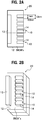
- FIG. 2A is a diagram that illustrates an exterior of an 8-element array sensor
- FIG. 2B is a perspective view of the 8-element array sensor.
- an 8-element array detector 20 includes eight terahertz wave detection elements 10 aligned in an array.
- the 8-element array sensor 20 includes the eight terahertz wave detection elements 10 each having 1 mm width and being aligned at 0.5 mm intervals.
- a longitudinal length of the terahertz wave detection element 10 of FIGs. 1A and 1B is 1 mm, and an interval between the electrodes between one terahertz wave detection element 10 and the other terahertz wave detection element 10 is 1.5 mm.
- THz detection can be made in a two-dimensional area of 8 ⁇ 8 by moving the 8-element array sensor 20 in either of an X direction and a Y direction.
- the 8-element array sensor 20 radiates the THz wave onto a surface of the single-walled carbon nanotubes film 12 of the terahertz wave detection element 10 and detects carriers that are THz excited in the low-dimensional electron.
- Carbon nanotubes have high electric conductivity and high flexibility with high mechanical strength.
- the carbon nanotubes absorb electromagnetic waves of an extremely wide frequency band including a region between frequency close to DC and ultraviolet light.
- the carbon nanotubes can absorb light of an extremely large frequency band from sub-terahertz to ultraviolet.
- the inventors previously indicated that the carbon nanotubes can be used for the terahertz wave detection device; however, the optimum conditions of the materials and the electrodes were unknown. This embodiment provides the optimum conditions of the materials and the electrodes.
- the carbon nanotube as the material has following characteristics.
- the single-walled carbon nanotubes film 12 is densely oriented such that the length direction is along ends of the first electrode 13 and the second electrode 14. Further accurate orientation is desired for improving the detection sensitivity.
- the single-walled carbon nanotubes film 12 is p-type. Otherwise the single-walled carbon nanotubes film 12 may be n-type or a combination of the p-type and the n-type.
- the single-walled carbon nanotubes film 12 is a carbon nanotube thin film having a film thickness of 50 ⁇ m, for example.
- the low-dimensional electron system material may be a graphene (described later) and a semiconductor hetero interface two-dimensional electron gas (2DEG).
- the first electrode 13 (source electrode) and the second electrode 14 (drain electrode) are made of metals.
- Metals that the inventors used for the electrodes are Au, Al, Mo, Ni, and Ti.
- a noble metal other than Au such as Cu, Ag, and Pt
- an aluminum group element other than Al such as Ga and In
- a chromium group element other than Mo such as Cr and W
- an iron group element other than Ni such as Fe and Co
- a tin group element other than Ti such as Zr, Sn, Hf, Pb, and Th
- a magnesium group element such as Be, Mg, and Zn
- an alloy of these metals can be used.
- the first electrode 13 (source electrode) and the second electrode 14 (drain electrode) are made of metals having asymmetric thermal conductivity.
- the thermal conductivity (degree of thermal conductivity) is a value obtained by dividing an amount of heat flowing through a unit area that is perpendicular to the heat flow per unit time by a temperature difference (temperature gradient) per unit length.
- the electrodes are made of different materials to provide a difference of the thermal conductivity between the electrodes.
- the difference of the thermal conductivity between the first electrode 13 and the second electrode 14 is preferred to be large (equal to or more than a predetermined difference) (described later).
- a combination of (Au, Al) and (Mo, Ni, Ti) makes large thermal conductivity of the electrode.
- an asymmetric electrode structure of the electrode thermal conductivity is implemented by using Au with high thermal conductivity for the first electrode 13 (source electrode) and using Ti with low thermal conductivity for the second electrode 14 (drain electrode).
- Au and Ti may be replaced with each other between the first electrode 13 and the second electrode 14.
- the length direction of the single-walled carbon nanotubes film between the first electrode 13 and the second electrode 14 is 1.5 mm, and an interval between the end of the first electrode 13 and the end of the second electrode 14 is 20 mm.
- FIG. 3 is a diagram that illustrates thermal conductivity [W/m ⁇ K] and response signals [ ⁇ A] (right vertical axis) of the electrode materials (Au, Al, Mo, Ni, and Ti).
- the response signals [ ⁇ A] are indicated as response currents.
- the thermal conductivity of the electrode materials is indicated by a line graph (left vertical axis) and the response signals are indicated by a bar graph (right vertical axis).
- the response current [ ⁇ A] of each electrode has sensitivity of a different value in the order of Au > Al > Mo > Ni > Ti.
- Au has the largest response current, and second is Al. Then the sensitivity drops by almost half from Al followed by Mo, Ni, and Ti.
- the above-described sensitivity relates to the thermal conductivity. That is, as illustrated in FIG. 3 , the higher the thermal conductivity, the higher the sensitivity.
- the detection sensitivity can be improved by increasing the electrode thermal conductivity.
- FIG. 4 is a diagram that illustrates a relationship of the response signal (response current) [ ⁇ A] and thickness of the electrode [nm].
- the thicker the electrode the higher the sensitivity.
- the response signal is increased by making the electrode thicker.
- the combination of (Au, Al) and (Mo, Ni, Ti) is used.
- Au with high thermal conductivity can be selected.
- a metal out of (Mo, Ni, Ti) can be selected for the other electrode. In this case, it is better to use Ti for the other electrode in order to increase the difference of the thermal conductivity between the electrodes.
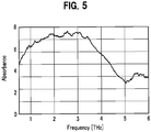
- FIG. 5 is a diagram that illustrates an electromagnetic wave absorption spectrum of the terahertz wave detection element 10 (single-walled carbon nanotubes film 12).
- the horizontal axis represents Frequency [THz] and the vertical axis represents electromagnetic wave absorbance.
- the terahertz wave detection element 10 can absorb the electromagnetic wave in a wide frequency band.
- the single-walled carbon nanotubes film 12 is densely oriented as an array such that the length direction is along the ends of the first electrode 13 and the second electrode 14. That is, this is a case where an oscillating electric field of the electromagnetic wave is parallel to the length direction of the single-walled carbon nanotubes film 12 (CNT array).
- the single-walled carbon nanotubes film 12 can absorb the electromagnetic wave in a wide frequency band.
- FIGs. 6A, 6B, and 6C include diagrams that illustrate I-V characteristics and results of THz response of the terahertz wave detection device 10 (under room temperature).
- the horizontal axis represents a source-drain voltage [mV] and the vertical axis represents a source-drain current [ ⁇ A].
- a narrow solid line of the I-V characteristic indicates a case where no THz irradiation occurs (Off) and a bold solid line of the I-V characteristic indicates a case where THz irradiation occurs (On).
- the I-V characteristic is linear, and shifting of the I-V characteristic is observed.
- the I-V characteristic is linear, and shifting of the I-V characteristic is observed.
- the I-V characteristic is linear, and shifting of the I-V characteristic is observed. Since every THz irradiation has no change in slope of the I-V characteristic (electric resistance is constant), this is not a simple bolometric effect (temperature rise effect due to THz absorption). It was found that the lower the thermal conductivity, the greater the THz response, by measuring dependency on the thermal conductivity of the substrate (chip carrier substrate 11) on which the single-walled carbon nanotubes film 12 (CNN array) is mounted.
- FIG. 7 is a diagram that illustrates a response signal (response current) [ ⁇ A] of an XY surface of the single-walled carbon nanotubes film 12. Darker-shaded areas in FIG. 7 is a part where the sensitivity is higher. On the actual screen, positive or negative and sensitivity of the response signal are detected and are displayed such that the left side of FIG. 7 and a positive side of the response signal [ ⁇ A] indicate positive of the signal (e.g., red color) and the right side of FIG. 7 and a negative side of the response signal [ ⁇ A] indicate negative of the signal (e.g., blue color), although they cannot be recognized on the drawing since FIG. 7 is monochrome.
- a response signal response current
- the sensitive parts are close to each electrode on two parts of the XY surface of the single-walled carbon nanotubes film 12. It was found that it is difficult to obtain accurate information for a structural reason because the sensitive parts are close to the electrodes.
- the inventors came up with an idea that the number of the sensitive part to be used may be one and it may be possible to obtain more accurate information if the sensitive part is located away from the electrodes.
- the asymmetric electrode structure is implemented by using metals with asymmetric thermal conductivity for the electrodes.
- the above-described sensitive part is located away from either of the electrodes by using Au with high thermal conductivity for the one electrode and using Ti with low thermal conductivity for the other electrode. This makes it possible to obtain an accurate image by detecting a response from only one side.
- FIG. 8 is a diagram that illustrates noise equivalent powers of the terahertz wave detection device 10.
- FIGs. 9A, 9B, and 9C include diagrams that illustrate I-V characteristics and results of THz response of the terahertz wave detection device 10 of a comparative example and the embodiment (under room temperature).
- the horizontal axis represents the source-drain voltage [mV] and the vertical axis represents the source-drain current [ ⁇ A].
- a narrow solid line and a narrow broken line of the I-V characteristic indicate a case where no THz irradiation occurs (Off) and a bold solid line and a bold broken line of the I-V characteristic indicate a case where THz irradiation occurs (On).
- FIG. 9A is a comparative example that the same kind of metal (Au-Au) is used for the first electrode 13 (source electrode) and the second electrode 14 (drain electrode).
- FIG. 9B illustrates an example that Au with high thermal conductivity is used for the first electrode 13 (source electrode) and Ti with low thermal conductivity is used for the second electrode 14 (drain electrode).
- the I-V characteristic is linear, and shifting of the I-V characteristic is observed. Note that the shifting of the I-V characteristic becomes the greatest when (Au-Ti) is used.
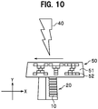
- FIG. 10 is a diagram that illustrates an overall configuration of a measurement system of the terahertz wave detection device.
- a metal mask 50 as a test object is irradiated with the Thz wave 40 of the infrared ray region from the above (IR irradiation).
- a light source of the THz is generated by a femtosecond laser and the like.
- the metal mask 50 is made by forming information 52 (in this case, letters X, Y, Z) on aluminum foil (non THz wave transmittable) 51 and superimposing a non-transparent (visible light) film (THz transmittable) on this aluminum foil 51 to be a mask.
- the 8-element array sensor 20 is arranged under this metal mask 50, and the 8-element array sensor 20 is moved in the XY directions (two-dimensional motion) with respect to the metal mask 50.
- the 8-element array sensor 20 is mounted to be irradiated with the THz wave 40 of the infrared ray region from the above, and the metal mask 50 is moved in a direction of an arrow (->) in FIG. 10 . That is, the 8-element array sensor 20 is moved and crossed in the one direction for observing the two-dimensional image.
- FIGs. 11A and 11B include diagrams that describe a method of observation using the measurement system in FIG. 10 , in which FIG. 11A is a diagram of the sample seen from below, and FIG. 11B is a diagram that illustrates an observed image of THz transmitted light.
- the metal mask 50 forms the letters 52 (X, Y, Z) on the aluminum foil 51 (e.g., the letter parts are cut off from the aluminum foil).
- the 8-element array sensor 20 is moved in the one direction for observing the two-dimensional image.
- the letters 52 of the metal mask 50 could be observed with high sensitivity and high accuracy. Since the terahertz wave detection elements 10 are arrayed, it is possible to obtain the two-dimensional image merely by moving the 8-element array sensor 20 in the one direction. Thus, high-speed observation is possible.
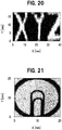
- FIG. 20 is a diagram that illustrates another example 1 of an observed image of THz transmitted light.
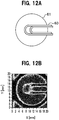
- FIGs. 12A and 12B include diagrams that describe an example of observing another sample using the measurement system in FIG. 10 , in which FIG. 12A is a diagram of the sample seen from below, and FIG. 12B is a diagram that illustrates an observed image of THz transmitted light.
- a part of a clip (soft iron) 60 (sample) is covered by a circle Ge plate 61.
- Ge of the Ge plate 61 is THz wave transmittable.
- Fe of the clip 60 is non THz wave transmittable. From the above, the clip 60 (sample) is hidden by the Ge plate 61 and is thus invisible.
- the two-dimensional image is observed by moving the 8-element array sensor 20 in the one direction.
- the clip 60 could be observed with high sensitivity and high accuracy. Since the terahertz wave detection elements 10 are arrayed, it is possible to obtain the two-dimensional image merely by moving and crossing the 8-element array sensor 20 in the one direction. Thus, high-speed observation is possible.
- FIG. 21 is a diagram that illustrates another example 2 of an observed image of THz transmitted light.
- FIGs. 13A, 13B, and 13C include diagrams that illustrate an overall configuration of a measurement system of the terahertz wave detection device.
- a 23-element array detector 70 includes 23 terahertz wave detection elements 10 aligned in an array on a flexible board 71.
- a material of the flexible board 71 may be anything such as a polyimide film.
- the single-walled carbon nanotubes film 12 (see FIGs 1A and 1B ) has both the high electric conductivity and mechanical strength and can be used for the flexible board 71 having flexibility.
- the 23-element array sensor 70 is a flexible sensor including 23 terahertz wave detection elements 10 each having 1 mm width and being aligned at 0.5 mm intervals on the flexible board 71.
- the 23-element array sensor 70 can be closely attached on a curved part on a living body such as a finger or an arm.
- a flexible bent mask 80 is made by forming the information 52 (in this case, letters X, Y, Z and graphic) on the aluminum foil (non THz wave transmittable) 51 and superimposing a non-transparent (visible light) film (THz transmittable) on this aluminum foil 51.
- the bent mask 80 (sample) is irradiated with the Thz wave 40 of the infrared ray region from the above (IR irradiation).
- a light source of the THz is generated by the femtosecond laser and the like.
- the bent mask 80 (sample) is irradiated with the THz wave 40 of the infrared ray region from the above, and the bent mask 80 is moved in a direction of an arrow (->) for observing the two-dimensional image.
- the letters and graphic 52 of the bent mask 80 could be observed with high sensitivity and high accuracy when observing the two-dimensional image by moving the bent mask 80 in the one direction. Since the terahertz wave detection elements 10 are arrayed, it is possible to obtain the two-dimensional image merely by moving the 23-element array sensor 70 in the one direction. Thus, high-speed observation is possible.
- FIGs. 14A, 14B, and 14C include diagrams that illustrate an application example of arranging the 23-element array sensor on the flexible board.
- FIG. 14A is an example of wrapping the flexible board 71 on which the 23-element array sensor 70 is arranged on a hand
- FIG. 14B is a diagram that illustrates an observed image of THz transmitted light.
- the terahertz wave detection element 10 includes the single-walled carbon nanotubes film 12 formed on the chip carrier substrate 11 and the first electrode 13 and the second electrode 14 opposingly arranged on the two-dimensional plane of the single-walled carbon nanotubes film 12, in which the first electrode 13 and the second electrode 14 are made of metals having different thermal conductivity.
- the difference of the thermal conductivity between the first electrode 13 and the second electrode 14 is preferred to be large (equal to or more than the predetermined difference).
- the asymmetric electrode structure is implemented by using the metals with asymmetric thermal conductivity for the electrodes.
- the sensitive part is away from either of the electrodes by using Au with high thermal conductivity for the first electrode 13 (source electrode) and using Ti with low thermal conductivity for the second electrode 14 (drain electrode). This makes it possible to obtain an accurate image by detecting a response from only one side.
- the 8-element array sensor 20 includes an array in which the eight terahertz wave detection elements 10 aligned. THz detection in the two-dimensional area of 8 ⁇ 8 can be made by moving the 8-element array sensor 20 in either of the X and Y directions. Since the terahertz wave detection elements 10 are arrayed, it is possible to obtain the two-dimensional image merely by moving the 8-element array sensor 20 in the one direction and high-speed observation with high sensitivity and high accuracy is possible.
- improvement of the detection sensitivity is confirmed by changing types and thickness of the electrodes. Imaging measurement using multi-elements allows an image that is not visible with visible light to be visible.
- image measurement of a region between sub-terahertz and infrared can be made by a single camera. Although the image measurement of 1 to 30 THz is possible for now, the image measurement of sub THz to hundreds THz is possible in principle.
- the 8-element array sensor 20 can be applied to sensing and medical application as a living body sensor and being attached on a human body by using its flexibility characteristic.
- FIG. 15A is a diagram that illustrates a configuration of a modification of the terahertz wave detection device
- FIG. 15B is a perspective view of the terahertz wave detection device as the modification.
- This modification is an example of using a graphene instead of the single-walled carbon nanotubes film.
- a terahertz wave detection element 10A includes a graphene 12A that is a two-dimensional system material and the first electrode 13 and the second electrode 14 opposingly arranged on a two-dimensional plane of the graphene 12A, in which the first electrode 13 and the second electrode 14 are made of metals having different thermal conductivity.
- the graphene 12A is preferred to have multiple layers including two or more layers.
- the graphene 12A is appropriate for the low-dimensional electron system material of the terahertz wave detection device 10.
- the graphene has a sheet structure with a single honeycomb atomic layer formed by sp 2 bonding of carbon atoms.
- the graphene has unique advantages such as high carrier mobility, optical wavelength independency (high transparency), and high optical non-linearity.
- the graphene is not limited to have a hexagonal cell structure merely made of the carbon atoms, and a certain kind of a substituent group/functional group may be linked to the hexagonal cell or otherwise a precursor such as an oxidized graphene may also exist.
- the graphene 12A is two-dimensionally arranged on the chip carrier substrate 11.
- the graphene 12A may be a graphene with a single layer instead of a graphene with multiple layers.
- the graphene has a cone band structure with no band gap and functions in any wavelength band with high carrier mobility and high transparency. This is preferable also in the context of a wavelength band of THz wave of the terahertz wave detection device 10A of this embodiment.
- the low-dimensional electron system material other than the graphene may be a phosphorene (atomic layer black phosphorus) and a transition metal dichalcogenide (MoS 2 , WS 2 , WSe 2 , and the like).
- the phosphorene and the molybdenum disulphide (MoS 2 ) have characteristics of a semiconductor including a band gap and high carrier mobility. Taking consideration of easiness of creating, the graphene, MoS 2 , and WS 2 are used in practice.
- the terahertz wave detection element 10 uses the photothermoelectric effect.
- FIG. 16 is a schematic diagram that illustrates the principle of the terahertz wave detection element of the present invention.
- a material A and a material B are comparable to a single-walled carbon nanotubes film (CNT) and an electrode or a p-type CNT and a n-type CNT.
- CNT carbon nanotubes film
- the material A and the material B contact with each other at a I part onto which the THz wave 40 of high temperature T h is radiated but do not contact with each other at a part away from the I part, which is the THz wave 40 irradiation part.
- THz wave 40 is radiated onto the I part at one end where the material A and the material B contact with each other.
- the I part absorbs the THz wave 40 and is heated to the high temperature T h . Since a II part at the other end is away from the I part, temperature of the II part is low temperature T o .
- Carriers are generated at the I part of the high temperature T h , while on the other hand almost no carriers are generated at the II part of the low temperature T o . Thus, density balance of the carriers is lost and the carriers flow from the I part to the II part. Once some amount of carriers move to the II part, moving of the carriers from the I part stops.
- the I part from which the carriers move has a charge opposite to the carriers, and the II part to which the carriers move has a charge same with the carriers. This generates a potential difference between the I part and the II part (thermoelectric power V) and a current flows between the I part and the II part.
- thermoelectric power V thermoelectric power
- Equation (1) Since the relative Seebeck coefficients S AB are expressed as (S A - S B ) in Equation (1), the greater a difference between the Seebeck coefficient S A of the material A and the Seebeck coefficient S B of the material B, the greater the thermoelectric power V.
- Equation (1) shows that the greater the temperature gradient (T h - T o ), the greater the thermoelectric power V.
- the greater the thermal conductivity difference between the material A and the material B the greater the temperature gradient (T h - T o ), and the greater the thermoelectric power V.
- thermoelectric power V when the first electrode 13 and the second electrode 14 are arranged as close as possible to each other for making the terahertz wave detection element 10 into a chip, since the first electrode 13 and the second electrode 14 made of the same kind of metal have the same thermal conductivity, the temperature difference between the first electrode 13 and the second electrode 14 is just about "0.” This makes the thermoelectric power V be close to "0" and it is difficult to detect the terahertz wave.
- first electrode 13 and the second electrode 14 are made of different kinds of metals, their thermal conductivity is different.
- the temperature difference of the first electrode 13 and the second electrode 14 is greater than the case where they are made of the same kind of metal. This allows the generated thermoelectric power V to be greater than the case of the same kind of metal.
- the case where the first electrode 13 and the second electrode 14 are made of different kinds of metals is more likely to be able to detect the THz wave 40 than the case of the same kind of metal.
- thermoelectric power V the greater the difference of the thermal conductivity between the first electrode 13 and the second electrode 14, the greater their temperature difference, and this allows much greater thermoelectric power V to be generated and higher sensitivity for detecting the THz wave 40 to be achieved.
- Table 1 shows thermal conductivity of the metals Cu, Au, Al, Mo, Ni, and Ti used for the first electrode 13 and the second electrode 14. [Table 1] Thermal Conductivity [W/(m ⁇ K)] Cu 403 Au 318 Al 237 Mo 138 Ni 90.9 Ti 21.9
- Table 2 shows combinations of the metals Cu, Au, Al, Mo, Ni, and Ti used for the first electrode 13 and the second electrode 14 and differences of the thermal conductivity (W/m ⁇ K) in each case.
- First Electrode Cu Au Al Mo Ni Ti Second Electrode Cu 0 85 166 265 312.1 381.1 Au 85 0 81 180 227.1 296.1 Al 166 81 0 99 146.1 215.1 Mo 265 180 99 0 47.1 116.1 Ni 312.1 227.1 146.1 47.1 0 69 Ti 318.1 296.1 215.1 116.1 69 0
- the combination of Cu and Ti has the greatest thermal conductivity difference that is 381.1 W/m ⁇ K.
- the combination of Au-Ti has the second greatest thermal conductivity difference that is 296.1 W/m ⁇ K.
- Au with the thermal conductivity of 318 W/m ⁇ K is used for the first electrode 13
- Ti with the thermal conductivity of 21.9 W/m ⁇ K is used for the second electrode 14.
- the combination of Mo and Ni has the smallest thermal conductivity difference that is 47.1 W/m ⁇ K.
- Mo with the thermal conductivity of 138 W/m ⁇ K is used for the first electrode 13
- Ni with the thermal conductivity of 90.9 W/m ⁇ K is used for the second electrode 14.
- the thermal conductivity difference is "0."
- Al is used for both the first electrode 13 and the second electrode 14.
- FIG. 17 illustrates thermal conductivity differences (W/m ⁇ K) (left vertical axis) and THz responses ( ⁇ A) (right vertical axis) of cases where the first electrode 13 and the second electrode 14 are applied with the combination of Au and Ti with the thermal conductivity difference of 296.1 W/m ⁇ K, the combination of Mo and Ni with the thermal conductivity difference of 47.1 W/m ⁇ K, and the combination of the same kind of metal Al with the thermal conductivity difference of 0.
- the thermal conductivity differences (W/m ⁇ K) (left vertical axis) are indicated by a line graph and the THz responses ( ⁇ A) (right vertical axis) are indicated by a bar graph.
- Evaluation conditions in FIG. 17 are a bundle size (bundle diameter) of 10 nm of the single-walled carbon nanotubes film 12, film thickness of 100 ⁇ m of the single-walled carbon nanotubes film 12, and each metal film thickness of 20 nm of the first electrode 13 and the second electrode 14.
- the bundle diameter is a diameter of a group of multiple carbon nanotubes keeping their fiber forms.
- the combination of Au and Ti with the thermal conductivity difference of 296.1 W/m ⁇ K corresponds to the THz response of about 2 ⁇ l A (right vertical axis).
- the combination of Mo and Ni with the thermal conductivity difference of 47.1 W/m ⁇ K corresponds to the THz response of about 1.5 ⁇ A (right vertical axis).
- the combination of the same kind of metal Al with the thermal conductivity difference of "0" corresponds to the THz response of about a little under 0.5 ⁇ A (right vertical axis).
- the strength of the photothermoelectric power V is determined depending on various parameters such as the thermal conductivity of electrode metals, the electric conductivity, and the Seebeck coefficient.
- the conditions of this embodiment 100 ⁇ m thickness of the single-walled carbon nanotubes film and each metal film thickness of 20 nm of the first electrode 13 and the second electrode 14) are thought to be determined dominantly depending on the thermal conductivity.
- the thermal conductivity difference between the first electrode 13 and the second electrode 14 has to be a value that at least makes the value of the response signal other than 0.
- the thermal conductivity difference between the first electrode 13 and the second electrode 14 may at least be set to a value that allows the detection signal to be obtained when the THz wave 40 is radiated onto the single-walled carbon nanotubes film 12.
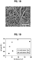
- FIG. 18 is a magnified photograph of the single-walled carbon nanotubes film 12 having a bundle diameter of about 10 nm.
- an object in a visible fiber form is the bundle.
- FIG. 19 is a diagram that illustrates a relationship of film thickness of the single-walled carbon nanotubes film 12 and a noise equivalent power (NEP) when the THz wave 40 of 29 THz is radiated.
- the horizontal axis represents the film thickness ( ⁇ m), and the vertical axis represents the NEP (pW/ Hz ).
- a black dot indicates a bundle diameter of about 200 nm and a white dot indicates a bundle diameter of about 10 nm.
- the bundle diameter is a diameter of a group of multiple carbon nanotubes keeping their fiber forms.
- the bundle diameter of about 200 nm has a higher NEP and higher sensitivity than the bundle diameter of about 10 nm in the single-walled carbon nanotubes film 12.
- the carbon nanotubes having a greater bundle diameter has better orientation than that having a smaller bundle diameter.
- the characteristics of the carbon nanotube fibers are likely to remain in the single-walled carbon nanotubes film 12 (carbon nanotubes film) with a greater bundle diameter.
- Fibers of the carbon nanotube have a great Seebeck coefficient.
- the single-walled carbon nanotubes film 12 (carbon nanotubes film) with a greater bundle diameter is sensitive.
- the single-walled carbon nanotubes film 12 is preferred to be oriented with a great bundle diameter to the extent possible, which is about 500 nm.
- the characteristics of the terahertz wave detection element 10 can be satisfied at least.
- the present invention is not limited to the above-described embodiments and includes another modification and application example without departing from a gist of the present invention stated in the claims.
- terahertz wave detection device uses a name of terahertz wave detection device; however, this is for the sake of convenience and the name may be terahertz wave detection unit or the like.
Landscapes
- Physics & Mathematics (AREA)
- Spectroscopy & Molecular Physics (AREA)
- General Physics & Mathematics (AREA)
- Chemical & Material Sciences (AREA)
- Engineering & Computer Science (AREA)
- Materials Engineering (AREA)
- Health & Medical Sciences (AREA)
- Nanotechnology (AREA)
- Toxicology (AREA)
- General Health & Medical Sciences (AREA)
- Immunology (AREA)
- Pathology (AREA)
- Biochemistry (AREA)
- Analytical Chemistry (AREA)
- Life Sciences & Earth Sciences (AREA)
- Photometry And Measurement Of Optical Pulse Characteristics (AREA)
- Investigating Or Analysing Materials By Optical Means (AREA)
Abstract

Description
- The invention relates to a terahertz wave detection device and an array sensor.
- Terahertz (THz) waves mean electromagnetic waves within a region of frequency of 0.1 to 30 THz (1 THz = 1012 Hz), the region including submillimeter waves and far-infrared rays having a wavelength of 0.01 mm to 3 mm.
- The terahertz waves have been unexplored because they are the higher frequency limit electronically controllable in electronics and also are the lower energy limit optically controllable in optics or photonics. For the terahertz waves, basic elements such as a light source and a detection unit are thus unexplored yet as compared to other frequency bands. Since the terahertz wave has a wavelength that is longer than that of visible light by two or three digits, the terahertz wave has a characteristic in which its spatial resolution for imaging is low.
-
Patent Literature 1 discloses a terahertz light detection device including a semiconductor chip in which a two-dimensional electron gas is formed within a certain range from the surface, and a carbon nanotube, a conductive source electrode, a conductive drain electrode, and a conductive gate electrode that are provided in close contact with the surface. The carbon nanotube extends along the surface of the semiconductor chip while its two ends are respectively connected to the source electrode and the drain electrode, and the gate electrode is located at a certain distance from a side surface of the carbon nanotube. The terahertz light detection device further includes an SD current detection circuit that detects an SD current between the source electrode and the drain electrode by applying a predetermined voltage between the electrodes, a gate voltage application circuit that applies a variable gate voltage between the source electrode and the gate electrode, and a magnetic field generation device that applies a variable magnetic field to the semiconductor chip. - For example, Non-patent
Literatures 1 to 4 disclose detection units that can detect frequency of the terahertz wave. Non-patentLiteratures - In contrast, Non-patent
Literature 4 discloses a new THz wave detection, spectrometry, and imaging technique, which uses functions of a low-dimensional electron system including a carbon nanotube (CNT) array, a graphene, and a semiconductor hetero interface two-dimensional electron gas (2DEG). Non-patentLiterature 4 discloses a new mechanism created with a hybrid structure in which carbon nanotube (CNT) quantum dots and the two-dimensional electron gas in the semiconductor are joined together and configured to read carriers excited in the two-dimensional electrons with a sensitive charge sensor made of the CNT. - Patent Literature 1: Japanese Patent Application Publication No.
2010-060284 -
- Non-patent Literature 1: Xiaowei He, Naoki Fujimura, J. Meagan Lloyd, Kristopher J. Erickson, A. Alec Talin, Qi Zhang, Weilu Gao, Qijia Jiang, Yukio Kawano, Robert H. Hauge, Francois Leonard and Junichiro Kono, "Carbon Nanotube Terahertz Detector," Nano Letters 14, 3953-3958 (2014)
- Non-patent Literature 2: Kristopher Erickson, Xiaowei He, A. Alec Talin, Bernice Mills, Robert H. Hauge, Takashi Iguchi, Naoki Fujimura, Yukio Kawano, Junichiro Kono, Francois Leonard, "Figure of Merit for Carbon Nanotube Photothermoelectric Detectors," ACS Nano 9, 11618-11627 (2015)
- Non-patent Literature 3: Yukio Kawano, "Terahertz Response of Carbon Nanotubes and Graphene," Journal of the Physical Society of Japan 84, 121010-1-9 (2015)
- Non-patent Literature 4: Yukio Kawano, "Terahertz detectors, spectrometers, and imagers based on low-dimensional electron systems," membership journal of The Japan Society of Applied Physics "OYO BUTURI" Vol. 84, pp. 643-647 (2015)
- Non-patent
literatures 1 to 4 have a problem that the optimum conditions for materials and electrodes are not identified in the case of a terahertz detection unit and an array sensor using the carbon nanotubes. - The invention was made in view of such a circumstance and has an object to provide a terahertz detection unit and an array sensor with improved detection sensitivity that can observe an accurate image.
- To solve the above problems, a first terahertz wave detection device according to the invention includes a low-dimensional electron system material formed on a substrate and a first electrode and a second electrode opposingly arranged on a two-dimensional plane of the low-dimensional electron system material, in which the first electrode and the second electrode are made of metals having different thermal conductivity.
- An array sensor according to the invention includes the terahertz wave detection devices aligned in an array, in which the array sensor radiates a THz wave onto a surface of the low-dimensional electron system material and detects carriers that are THz excited in the low-dimensional electron.
- A second terahertz wave detection device according to the present invention includes a carbon nanotube film and a first electrode arranged on one side of the carbon nanotube film and a second electrode arranged on the other side of the carbon nanotube film, in which the first electrode and the second electrode have different or the same thermal conductivity.
- According to the present invention, it is possible to provide a terahertz detection unit with improved detection sensitivity that can observe an accurate image.
-
-
FIG. 1A is a diagram that illustrates a configuration of a terahertz wave detection device according to an embodiment of the present invention, andFIG. 1B is a perspective view of the terahertz wave detection device. -
FIG. 2A is a diagram that illustrates an exterior of an 8-element array sensor of the terahertz wave detection device according to the embodiment, andFIG. 2B is a perspective view of the 8-element array sensor. -
FIG. 3 is a diagram that illustrates thermal conductivity and sensitivity of electrode materials (Au, Al, Mo, Ni, and Ti) of the terahertz wave detection device according to the embodiment. -
FIG. 4 is a diagram that illustrates a relationship of response sensitivity and thickness of the electrode of the terahertz wave detection device according to the embodiment. -
FIG. 5 is a diagram that illustrates an electromagnetic wave absorption spectrum of the terahertz wave detection device according to the embodiment. -
FIGs. 6A, 6B and 6C include diagrams that illustrate I-V characteristics and results of THz response of the terahertz wave detection device according to the embodiment, in whichFIG. 6A illustrates shifting observation of the I-V characteristic when THz irradiation of 0.14 THz occurs,FIG. 6B illustrates shifting observation of the I-V characteristic when THz irradiation of 14 THz occurs, andFIG. 6C illustrates shifting observation of the I-V characteristic when THz irradiation of 30 THz occurs. -
FIG. 7 is a diagram that illustrates sensitivity of an XY surface of a single-walled carbon nanotubes film of the terahertz wave detection device according to the embodiment. -
FIG. 8 is a diagram that illustrates noise equivalent powers of the terahertz wave detection device according to the embodiment. -
FIGs. 9A and 9B include diagrams that illustrate I-V characteristics and results of THz response of the terahertz wave detection device of a comparative example and the embodiment, in whichFIG. 9A illustrates the comparative example that the same kind of metal (Au-Au) is used for a first electrode (source electrode) and a second electrode (drain electrode), andFIG. 9B illustrates an example that Au with high thermal conductivity is used for the first electrode (source electrode) and Ti with low thermal conductivity is used for the second electrode (drain electrode). -
FIG. 10 is a diagram that illustrates an overall configuration of a measurement system of the terahertz wave detection device according to the embodiment. -
FIGs. 11A and 11B include diagrams that describe a method of observation using the measurement system inFIG. 10 , in whichFIG. 11A is a diagram of a sample seen from below, andFIG. 11B is a diagram that illustrates an observed image of THz transmitted light. -
FIGs. 12A and 12B include diagrams that describe an example of observing another sample using the measurement system inFIG. 10 , in whichFIG. 12A is a diagram of the sample seen from below, andFIG. 12B is a diagram that illustrates an observed image of THz transmitted light. -
FIGs. 13A, 13B and 13C include diagrams that illustrate an overall configuration of a measurement system of the terahertz wave detection device according to the embodiment, in whichFIG. 13A is an example of the overall configuration of the measurement system,FIG. 13B is an example of a bent mask, andFIG. 13C is an example of an observed two-dimensional image. -
FIGs. 14A and 14B include diagrams that illustrate an application example of arranging a 23-element array sensor of the terahertz wave detection device according to the embodiment on a flexible board, in whichFIG. 14A is an example of wrapping a flexible board on which the 23-element array sensor is arranged on a hand, andFIG. 14B is a diagram that illustrates an observed image of THz transmitted light. -
FIG. 15A is a diagram that illustrates a configuration of a modification of the terahertz wave detection device according to the embodiment, andFIG. 15B is a perspective view of the terahertz wave detection device as the modification. -
FIG. 16 is a schematic diagram that illustrates a principle of a terahertz wave detection element of the present invention. -
FIG. 17 is a diagram that illustrates thermal conductivity differences and THz responses of cases where the first electrode and the second electrode are applied with a combination of Au and Ti with a thermal conductivity difference of 296.1 W/m·K, a combination of Mo and Ni with a thermal conductivity difference of 47.1 W/m·K, and a combination of the same kind of metal Al with a thermal conductivity difference of 0. -
FIG. 18 is a magnified photograph of a single-walled carbon nanotubes film having a bundle diameter of about 10 nm. -
FIG. 19 is a diagram that illustrates a relationship of film thickness of the single-walled carbon nanotubes film and a noise equivalent power when a THz wave of 29 THz is radiated. -
FIG. 20 is a diagram that illustrates another example 1 of an observed image of THz transmitted light. -
FIG. 21 is a diagram that illustrates another example 2 of an observed image of THz transmitted light. - Hereinafter, embodiments of the present invention will be described in detail with reference to the drawings.
-
FIG. 1A is a diagram that illustrates a configuration of a terahertz wave detection device according to one embodiment of the present invention, andFIG. 1B is a perspective view of the terahertz wave detection device. - The terahertz wave detection device of this embodiment provides the optimum conditions of materials and electrodes.
- As illustrated in
FIGs. 1A and 1B , a terahertz wave detection element 10 (terahertz wave detection device) includes a single-walled carbon nanotubes film (SWCNTs film) 12 (low-dimensional electron system material) accurately oriented in the horizontal direction on achip carrier substrate 11, afirst electrode 13 having a first thermal conductivity on one end of the single-walledcarbon nanotubes film 12, and asecond electrode 14 having a second thermal conductivity on the other end of the single-walledcarbon nanotubes film 12. - That is, the terahertz
wave detection element 10 includes the single-walledcarbon nanotubes film 12 formed on thechip carrier substrate 11 and thefirst electrode 13 and thesecond electrode 14 opposingly arranged on a two-dimensional plane of the single-walledcarbon nanotubes film 12, in which thefirst electrode 13 and thesecond electrode 14 are made of metals having different thermal conductivity. Thechip carrier substrate 11 may be made of any material. - A
battery 30 and anammeter 35 are connected between thefirst electrode 13 and thesecond electrode 14. Since a positive side of thebattery 30 is thefirst electrode 13 inFIGs. 1A and 1B , thefirst electrode 13 is called a source electrode and thesecond electrode 14 is called a drain electrode in some cases. - The single-walled
carbon nanotubes film 12 between thefirst electrode 13 and thesecond electrode 14 is irradiated with aTHz wave 40 of an infrared ray region (IR irradiation). -
FIG. 2A is a diagram that illustrates an exterior of an 8-element array sensor, andFIG. 2B is a perspective view of the 8-element array sensor. - As illustrated in
FIGs. 2A and 2B , an 8-element array detector 20 includes eight terahertz wavedetection elements 10 aligned in an array. When the 8-element array sensor is stored in a small package for use, the small package is desirably vacuum locked, but the small package may not be vacuum locked. The 8-element array sensor 20 includes the eight terahertzwave detection elements 10 each having 1 mm width and being aligned at 0.5 mm intervals. InFIG. 2A , a longitudinal length of the terahertzwave detection element 10 ofFIGs. 1A and 1B is 1 mm, and an interval between the electrodes between one terahertzwave detection element 10 and the other terahertzwave detection element 10 is 1.5 mm. THz detection can be made in a two-dimensional area of 8 × 8 by moving the 8-element array sensor 20 in either of an X direction and a Y direction. - The 8-
element array sensor 20 radiates the THz wave onto a surface of the single-walledcarbon nanotubes film 12 of the terahertzwave detection element 10 and detects carriers that are THz excited in the low-dimensional electron. - Carbon nanotubes have high electric conductivity and high flexibility with high mechanical strength. The carbon nanotubes absorb electromagnetic waves of an extremely wide frequency band including a region between frequency close to DC and ultraviolet light. Particularly, the carbon nanotubes can absorb light of an extremely large frequency band from sub-terahertz to ultraviolet. The inventors previously indicated that the carbon nanotubes can be used for the terahertz wave detection device; however, the optimum conditions of the materials and the electrodes were unknown. This embodiment provides the optimum conditions of the materials and the electrodes. First, the carbon nanotube as the material has following characteristics.
- The single-walled
carbon nanotubes film 12 is densely oriented such that the length direction is along ends of thefirst electrode 13 and thesecond electrode 14. Further accurate orientation is desired for improving the detection sensitivity. - As an example, the single-walled
carbon nanotubes film 12 is p-type. Otherwise the single-walledcarbon nanotubes film 12 may be n-type or a combination of the p-type and the n-type. - The single-walled
carbon nanotubes film 12 is a carbon nanotube thin film having a film thickness of 50 µm, for example. - Other than the above-mentioned single-walled carbon nanotubes film, the low-dimensional electron system material may be a graphene (described later) and a semiconductor hetero interface two-dimensional electron gas (2DEG).
- The first electrode 13 (source electrode) and the second electrode 14 (drain electrode) are made of metals. Metals that the inventors used for the electrodes are Au, Al, Mo, Ni, and Ti. However, it may be considered that a noble metal other than Au such as Cu, Ag, and Pt, an aluminum group element other than Al such as Ga and In, a chromium group element other than Mo such as Cr and W, an iron group element other than Ni such as Fe and Co, a tin group element other than Ti such as Zr, Sn, Hf, Pb, and Th, a magnesium group element such as Be, Mg, and Zn, and an alloy of these metals can be used.
- The first electrode 13 (source electrode) and the second electrode 14 (drain electrode) are made of metals having asymmetric thermal conductivity. The thermal conductivity (degree of thermal conductivity) is a value obtained by dividing an amount of heat flowing through a unit area that is perpendicular to the heat flow per unit time by a temperature difference (temperature gradient) per unit length. The electrodes are made of different materials to provide a difference of the thermal conductivity between the electrodes.
- The difference of the thermal conductivity between the
first electrode 13 and thesecond electrode 14 is preferred to be large (equal to or more than a predetermined difference) (described later). Among the electrode materials indicated inFIG. 3 , a combination of (Au, Al) and (Mo, Ni, Ti) makes large thermal conductivity of the electrode. - For example, an asymmetric electrode structure of the electrode thermal conductivity is implemented by using Au with high thermal conductivity for the first electrode 13 (source electrode) and using Ti with low thermal conductivity for the second electrode 14 (drain electrode). In this case, Au and Ti may be replaced with each other between the
first electrode 13 and thesecond electrode 14. - As an example, the length direction of the single-walled carbon nanotubes film between the
first electrode 13 and thesecond electrode 14 is 1.5 mm, and an interval between the end of thefirst electrode 13 and the end of thesecond electrode 14 is 20 mm. -
FIG. 3 is a diagram that illustrates thermal conductivity [W/m·K] and response signals [µA] (right vertical axis) of the electrode materials (Au, Al, Mo, Ni, and Ti). The response signals [µA] are indicated as response currents. InFIG. 3 , the thermal conductivity of the electrode materials is indicated by a line graph (left vertical axis) and the response signals are indicated by a bar graph (right vertical axis). - As illustrated in
FIG. 3 , the response current [µA] of each electrode has sensitivity of a different value in the order of Au > Al > Mo > Ni > Ti. Among the electrode materials indicated inFIG. 3 , Au has the largest response current, and second is Al. Then the sensitivity drops by almost half from Al followed by Mo, Ni, and Ti. - The above-described sensitivity relates to the thermal conductivity. That is, as illustrated in
FIG. 3 , the higher the thermal conductivity, the higher the sensitivity. The detection sensitivity can be improved by increasing the electrode thermal conductivity. -
FIG. 4 is a diagram that illustrates a relationship of the response signal (response current) [µA] and thickness of the electrode [nm]. - As illustrated in
FIG. 4 , the thicker the electrode, the higher the sensitivity. The response signal is increased by making the electrode thicker. - As described above, in terms of using metals with asymmetric thermal conductivity, among the electrode materials indicated in
FIG. 3 , the combination of (Au, Al) and (Mo, Ni, Ti) is used. In terms of improving the detection sensitivity, Au with high thermal conductivity can be selected. Thus, when Au is selected for one electrode, a metal out of (Mo, Ni, Ti) can be selected for the other electrode. In this case, it is better to use Ti for the other electrode in order to increase the difference of the thermal conductivity between the electrodes. -
FIG. 5 is a diagram that illustrates an electromagnetic wave absorption spectrum of the terahertz wave detection element 10 (single-walled carbon nanotubes film 12). The horizontal axis represents Frequency [THz] and the vertical axis represents electromagnetic wave absorbance. - As illustrated in
FIG. 5 , the terahertzwave detection element 10 can absorb the electromagnetic wave in a wide frequency band. - As described above, the single-walled
carbon nanotubes film 12 is densely oriented as an array such that the length direction is along the ends of thefirst electrode 13 and thesecond electrode 14. That is, this is a case where an oscillating electric field of the electromagnetic wave is parallel to the length direction of the single-walled carbon nanotubes film 12 (CNT array). Thus, the single-walledcarbon nanotubes film 12 can absorb the electromagnetic wave in a wide frequency band. -
FIGs. 6A, 6B, and 6C include diagrams that illustrate I-V characteristics and results of THz response of the terahertz wave detection device 10 (under room temperature). The horizontal axis represents a source-drain voltage [mV] and the vertical axis represents a source-drain current [µA]. InFIGs. 6A, 6B, and 6C , a narrow solid line of the I-V characteristic indicates a case where no THz irradiation occurs (Off) and a bold solid line of the I-V characteristic indicates a case where THz irradiation occurs (On). - As illustrated in
FIG. 6A , when there is THz irradiation of 0.14 THz, the I-V characteristic is linear, and shifting of the I-V characteristic is observed. - As illustrated in
FIG. 6B , when there is THz irradiation of 1.4 THz, the I-V characteristic is linear, and shifting of the I-V characteristic is observed. - As illustrated in
FIG. 6C , when there is THz irradiation of 30 THz, the I-V characteristic is linear, and shifting of the I-V characteristic is observed. Since every THz irradiation has no change in slope of the I-V characteristic (electric resistance is constant), this is not a simple bolometric effect (temperature rise effect due to THz absorption). It was found that the lower the thermal conductivity, the greater the THz response, by measuring dependency on the thermal conductivity of the substrate (chip carrier substrate 11) on which the single-walled carbon nanotubes film 12 (CNN array) is mounted. This fact means that the heat that is generated as a result of the THz irradiation is not released through the substrate and the THz response is increased the more the heat is accumulated in the CNT, and thus the photothermoelectric effect is expected as a THz detection mechanism. -
FIG. 7 is a diagram that illustrates a response signal (response current) [µA] of an XY surface of the single-walledcarbon nanotubes film 12. Darker-shaded areas inFIG. 7 is a part where the sensitivity is higher. On the actual screen, positive or negative and sensitivity of the response signal are detected and are displayed such that the left side ofFIG. 7 and a positive side of the response signal [µA] indicate positive of the signal (e.g., red color) and the right side ofFIG. 7 and a negative side of the response signal [µA] indicate negative of the signal (e.g., blue color), although they cannot be recognized on the drawing sinceFIG. 7 is monochrome. The sensitive parts are close to each electrode on two parts of the XY surface of the single-walledcarbon nanotubes film 12. It was found that it is difficult to obtain accurate information for a structural reason because the sensitive parts are close to the electrodes. The inventors came up with an idea that the number of the sensitive part to be used may be one and it may be possible to obtain more accurate information if the sensitive part is located away from the electrodes. Thus, the asymmetric electrode structure is implemented by using metals with asymmetric thermal conductivity for the electrodes. For example, the above-described sensitive part is located away from either of the electrodes by using Au with high thermal conductivity for the one electrode and using Ti with low thermal conductivity for the other electrode. This makes it possible to obtain an accurate image by detecting a response from only one side. -
FIG. 8 is a diagram that illustrates noise equivalent powers of the terahertzwave detection device 10. - As illustrated in
FIG. 8 , excellent detection sensitivity with noise equivalent powers of 10-10 to 10-11 A/Hz1/2 could be obtained in the extremely wide frequency band including the region between frequency close to DC and ultraviolet light. -
FIGs. 9A, 9B, and 9C include diagrams that illustrate I-V characteristics and results of THz response of the terahertzwave detection device 10 of a comparative example and the embodiment (under room temperature). The horizontal axis represents the source-drain voltage [mV] and the vertical axis represents the source-drain current [µA]. InFIGs. 9A, 9B, and 9C , a narrow solid line and a narrow broken line of the I-V characteristic indicate a case where no THz irradiation occurs (Off) and a bold solid line and a bold broken line of the I-V characteristic indicate a case where THz irradiation occurs (On). -
FIG. 9A is a comparative example that the same kind of metal (Au-Au) is used for the first electrode 13 (source electrode) and the second electrode 14 (drain electrode). - As illustrated in
FIG. 9A , in the comparative example, no shifting of the I-V characteristic due to the THz irradiation is observed. -
FIG. 9B illustrates an example that Au with high thermal conductivity is used for the first electrode 13 (source electrode) and Ti with low thermal conductivity is used for the second electrode 14 (drain electrode). - As illustrated in
FIG. 9B , with the THz irradiation, the I-V characteristic is linear, and shifting of the I-V characteristic is observed. Note that the shifting of the I-V characteristic becomes the greatest when (Au-Ti) is used. - Next, an example of measuring using the 8-
element array sensor 20 that is made as a prototype based on the above-mentioned optimal values is described below. -
FIG. 10 is a diagram that illustrates an overall configuration of a measurement system of the terahertz wave detection device. - As illustrated in
FIG. 10 , ametal mask 50 as a test object (sample) is irradiated with theThz wave 40 of the infrared ray region from the above (IR irradiation). A light source of the THz is generated by a femtosecond laser and the like. Themetal mask 50 is made by forming information 52 (in this case, letters X, Y, Z) on aluminum foil (non THz wave transmittable) 51 and superimposing a non-transparent (visible light) film (THz transmittable) on thisaluminum foil 51 to be a mask. - The 8-
element array sensor 20 is arranged under thismetal mask 50, and the 8-element array sensor 20 is moved in the XY directions (two-dimensional motion) with respect to themetal mask 50. - Otherwise, as illustrated in
FIG. 10 , the 8-element array sensor 20 is mounted to be irradiated with theTHz wave 40 of the infrared ray region from the above, and themetal mask 50 is moved in a direction of an arrow (->) inFIG. 10 . That is, the 8-element array sensor 20 is moved and crossed in the one direction for observing the two-dimensional image. -
FIGs. 11A and 11B include diagrams that describe a method of observation using the measurement system inFIG. 10 , in whichFIG. 11A is a diagram of the sample seen from below, andFIG. 11B is a diagram that illustrates an observed image of THz transmitted light. - As illustrated in
FIG. 11A , the metal mask 50 (sample) forms the letters 52 (X, Y, Z) on the aluminum foil 51 (e.g., the letter parts are cut off from the aluminum foil). - As illustrated in
FIG. 10 , the 8-element array sensor 20 is moved in the one direction for observing the two-dimensional image. As illustrated inFIGs. 11B and20 , theletters 52 of themetal mask 50 could be observed with high sensitivity and high accuracy. Since the terahertzwave detection elements 10 are arrayed, it is possible to obtain the two-dimensional image merely by moving the 8-element array sensor 20 in the one direction. Thus, high-speed observation is possible. - Note that
FIG. 20 is a diagram that illustrates another example 1 of an observed image of THz transmitted light. -
FIGs. 12A and 12B include diagrams that describe an example of observing another sample using the measurement system inFIG. 10 , in whichFIG. 12A is a diagram of the sample seen from below, andFIG. 12B is a diagram that illustrates an observed image of THz transmitted light. - As illustrated in
FIG. 12A , a part of a clip (soft iron) 60 (sample) is covered by a circle Ge plate 61. In this case, Ge of the Ge plate 61 is THz wave transmittable. Fe of theclip 60 is non THz wave transmittable. From the above, the clip 60 (sample) is hidden by the Ge plate 61 and is thus invisible. - As illustrated in
FIG. 10 , the two-dimensional image is observed by moving the 8-element array sensor 20 in the one direction. As illustrated inFIGs. 12B and21 , theclip 60 could be observed with high sensitivity and high accuracy. Since the terahertzwave detection elements 10 are arrayed, it is possible to obtain the two-dimensional image merely by moving and crossing the 8-element array sensor 20 in the one direction. Thus, high-speed observation is possible. - Note that
FIG. 21 is a diagram that illustrates another example 2 of an observed image of THz transmitted light. -
FIGs. 13A, 13B, and 13C include diagrams that illustrate an overall configuration of a measurement system of the terahertz wave detection device. - As illustrated in
FIGs. 13A, 13B, and 13C , a 23-element array detector 70 includes 23 terahertz wavedetection elements 10 aligned in an array on aflexible board 71. A material of theflexible board 71 may be anything such as a polyimide film. The single-walled carbon nanotubes film 12 (seeFIGs 1A and 1B ) has both the high electric conductivity and mechanical strength and can be used for theflexible board 71 having flexibility. The 23-element array sensor 70 is a flexible sensor including 23 terahertz wavedetection elements 10 each having 1 mm width and being aligned at 0.5 mm intervals on theflexible board 71. The 23-element array sensor 70 can be closely attached on a curved part on a living body such as a finger or an arm. - As illustrated in
FIG. 13B , a flexiblebent mask 80 is made by forming the information 52 (in this case, letters X, Y, Z and graphic) on the aluminum foil (non THz wave transmittable) 51 and superimposing a non-transparent (visible light) film (THz transmittable) on thisaluminum foil 51. - The bent mask 80 (sample) is irradiated with the
Thz wave 40 of the infrared ray region from the above (IR irradiation). A light source of the THz is generated by the femtosecond laser and the like. - As illustrated in
FIG. 13A , the bent mask 80 (sample) is irradiated with theTHz wave 40 of the infrared ray region from the above, and thebent mask 80 is moved in a direction of an arrow (->) for observing the two-dimensional image. - As illustrated in
FIG. 13C , the letters and graphic 52 of thebent mask 80 could be observed with high sensitivity and high accuracy when observing the two-dimensional image by moving thebent mask 80 in the one direction. Since the terahertzwave detection elements 10 are arrayed, it is possible to obtain the two-dimensional image merely by moving the 23-element array sensor 70 in the one direction. Thus, high-speed observation is possible. -
FIGs. 14A, 14B, and 14C include diagrams that illustrate an application example of arranging the 23-element array sensor on the flexible board.FIG. 14A is an example of wrapping theflexible board 71 on which the 23-element array sensor 70 is arranged on a hand, andFIG. 14B is a diagram that illustrates an observed image of THz transmitted light. - As illustrated in
FIGs. 14A, 14b, and 14C , passive imaging of radiation from the hand with no external light source could be observed. This is expected as a first step for medical application. - As described above, the terahertz
wave detection element 10 according to this embodiment includes the single-walledcarbon nanotubes film 12 formed on thechip carrier substrate 11 and thefirst electrode 13 and thesecond electrode 14 opposingly arranged on the two-dimensional plane of the single-walledcarbon nanotubes film 12, in which thefirst electrode 13 and thesecond electrode 14 are made of metals having different thermal conductivity. The difference of the thermal conductivity between thefirst electrode 13 and thesecond electrode 14 is preferred to be large (equal to or more than the predetermined difference). - In this way, the asymmetric electrode structure is implemented by using the metals with asymmetric thermal conductivity for the electrodes. For example, the sensitive part is away from either of the electrodes by using Au with high thermal conductivity for the first electrode 13 (source electrode) and using Ti with low thermal conductivity for the second electrode 14 (drain electrode). This makes it possible to obtain an accurate image by detecting a response from only one side.
- The 8-
element array sensor 20 includes an array in which the eight terahertzwave detection elements 10 aligned. THz detection in the two-dimensional area of 8 × 8 can be made by moving the 8-element array sensor 20 in either of the X and Y directions. Since the terahertzwave detection elements 10 are arrayed, it is possible to obtain the two-dimensional image merely by moving the 8-element array sensor 20 in the one direction and high-speed observation with high sensitivity and high accuracy is possible. - In this embodiment, improvement of the detection sensitivity is confirmed by changing types and thickness of the electrodes. Imaging measurement using multi-elements allows an image that is not visible with visible light to be visible.
- In addition, image measurement of a region between sub-terahertz and infrared can be made by a single camera. Although the image measurement of 1 to 30 THz is possible for now, the image measurement of sub THz to hundreds THz is possible in principle.
- It is also possible to create a bent camera.
- Moreover, the 8-
element array sensor 20 can be applied to sensing and medical application as a living body sensor and being attached on a human body by using its flexibility characteristic. -
FIG. 15A is a diagram that illustrates a configuration of a modification of the terahertz wave detection device, andFIG. 15B is a perspective view of the terahertz wave detection device as the modification. - This modification is an example of using a graphene instead of the single-walled carbon nanotubes film.
- As illustrated in
FIGs. 15A and 15B , a terahertzwave detection element 10A includes agraphene 12A that is a two-dimensional system material and thefirst electrode 13 and thesecond electrode 14 opposingly arranged on a two-dimensional plane of thegraphene 12A, in which thefirst electrode 13 and thesecond electrode 14 are made of metals having different thermal conductivity. - The
graphene 12A is preferred to have multiple layers including two or more layers. - Likewise the single-walled
carbon nanotubes film 12, thegraphene 12A is appropriate for the low-dimensional electron system material of the terahertzwave detection device 10. - The graphene has a sheet structure with a single honeycomb atomic layer formed by sp2 bonding of carbon atoms. The graphene has unique advantages such as high carrier mobility, optical wavelength independency (high transparency), and high optical non-linearity. The graphene is not limited to have a hexagonal cell structure merely made of the carbon atoms, and a certain kind of a substituent group/functional group may be linked to the hexagonal cell or otherwise a precursor such as an oxidized graphene may also exist. In this modification, the
graphene 12A is two-dimensionally arranged on thechip carrier substrate 11. In addition, thegraphene 12A may be a graphene with a single layer instead of a graphene with multiple layers. - The graphene has a cone band structure with no band gap and functions in any wavelength band with high carrier mobility and high transparency. This is preferable also in the context of a wavelength band of THz wave of the terahertz
wave detection device 10A of this embodiment. - The low-dimensional electron system material other than the graphene may be a phosphorene (atomic layer black phosphorus) and a transition metal dichalcogenide (MoS2, WS2, WSe2, and the like). Note that the phosphorene and the molybdenum disulphide (MoS2) have characteristics of a semiconductor including a band gap and high carrier mobility. Taking consideration of easiness of creating, the graphene, MoS2, and WS2 are used in practice.
- Next, a principle of the terahertz wave detection element (terahertz wave detection device) 10 is described.
- The terahertz
wave detection element 10 uses the photothermoelectric effect. -
FIG. 16 is a schematic diagram that illustrates the principle of the terahertz wave detection element of the present invention. - A material A and a material B are comparable to a single-walled carbon nanotubes film (CNT) and an electrode or a p-type CNT and a n-type CNT.
- The material A and the material B contact with each other at a I part onto which the
THz wave 40 of high temperature Th is radiated but do not contact with each other at a part away from the I part, which is theTHz wave 40 irradiation part. - It is assumed that the
THz wave 40 is radiated onto the I part at one end where the material A and the material B contact with each other. - Then, the I part absorbs the
THz wave 40 and is heated to the high temperature Th. Since a II part at the other end is away from the I part, temperature of the II part is low temperature To. - This generates a temperature difference between the I part and the II part, and the temperature gradient occurs.
- Carriers are generated at the I part of the high temperature Th, while on the other hand almost no carriers are generated at the II part of the low temperature To. Thus, density balance of the carriers is lost and the carriers flow from the I part to the II part. Once some amount of carriers move to the II part, moving of the carriers from the I part stops.
- The I part from which the carriers move has a charge opposite to the carriers, and the II part to which the carriers move has a charge same with the carriers. This generates a potential difference between the I part and the II part (thermoelectric power V) and a current flows between the I part and the II part.
- That is, heat (temperature gradient) is generated by absorption of the
THz wave 40 into the single-walled carbon nanotubes film 12 (seeFIG. 1A ), and thus the potential difference (thermoelectric power V) occurs. - The thermoelectric power V is expressed by following Equation (1).
[Math. 1]
- V: heat power
- SAB: relative Seebeck coefficient
- Th: temperature of I part
- To: temperature of II part
- SA is a Seebeck coefficient of the material A and SB is a Seebeck coefficient of the material B.
- Since the relative Seebeck coefficients SAB are expressed as (SA - SB) in Equation (1), the greater a difference between the Seebeck coefficient SA of the material A and the Seebeck coefficient SB of the material B, the greater the thermoelectric power V.
- Equation (1) shows that the greater the temperature gradient (Th - To), the greater the thermoelectric power V. Thus, the greater the thermal conductivity difference between the material A and the material B, the greater the temperature gradient (Th - To), and the greater the thermoelectric power V.
- In a case where the above-described relationship is applied to the terahertz
wave detection element 10 illustrated inFIG. 1A , at the irradiation of theTHz wave 40 on the single-walledcarbon nanotubes film 12, temperature of the electrode close to the irradiation part of the single-walled carbon nanotubes film 12 (one of thefirst electrode 13 and the second electrode 14) becomes relatively high, and temperature of the electrode away from the irradiation part (the other one of thefirst electrode 13 and the second electrode 14) becomes relatively low. - In this case, when the
first electrode 13 and thesecond electrode 14 are arranged as close as possible to each other for making the terahertzwave detection element 10 into a chip, since thefirst electrode 13 and thesecond electrode 14 made of the same kind of metal have the same thermal conductivity, the temperature difference between thefirst electrode 13 and thesecond electrode 14 is just about "0." This makes the thermoelectric power V be close to "0" and it is difficult to detect the terahertz wave. - On the other hand, when the
first electrode 13 and thesecond electrode 14 are made of different kinds of metals, their thermal conductivity is different. Thus, when thefirst electrode 13 and thesecond electrode 14 are arranged as close as possible to each other, since their thermal conductivity is different, the temperature difference of thefirst electrode 13 and thesecond electrode 14 is greater than the case where they are made of the same kind of metal. This allows the generated thermoelectric power V to be greater than the case of the same kind of metal. - In other words, the case where the
first electrode 13 and thesecond electrode 14 are made of different kinds of metals is more likely to be able to detect theTHz wave 40 than the case of the same kind of metal. - That is, the greater the difference of the thermal conductivity between the
first electrode 13 and thesecond electrode 14, the greater their temperature difference, and this allows much greater thermoelectric power V to be generated and higher sensitivity for detecting theTHz wave 40 to be achieved. - An evaluation is made to see how the sensitivity of the terahertz
wave detection element 10 changes depending on the difference of the thermal conductivity between thefirst electrode 13 and thesecond electrode 14. - Table 1 shows thermal conductivity of the metals Cu, Au, Al, Mo, Ni, and Ti used for the
first electrode 13 and thesecond electrode 14.[Table 1] Thermal Conductivity [W/(m·K)] Cu 403 Au 318 Al 237 Mo 138 Ni 90.9 Ti 21.9 - Table 2 shows combinations of the metals Cu, Au, Al, Mo, Ni, and Ti used for the
first electrode 13 and thesecond electrode 14 and differences of the thermal conductivity (W/m·K) in each case.[Table 2] First Electrode Cu Au Al Mo Ni Ti Second Electrode Cu 0 85 166 265 312.1 381.1 Au 85 0 81 180 227.1 296.1 Al 166 81 0 99 146.1 215.1 Mo 265 180 99 0 47.1 116.1 Ni 312.1 227.1 146.1 47.1 0 69 Ti 318.1 296.1 215.1 116.1 69 0 - According to Tables 1 and 2, among these metals, the combination of Cu and Ti has the greatest thermal conductivity difference that is 381.1 W/m·K.
- The combination of Au-Ti has the second greatest thermal conductivity difference that is 296.1 W/m·K. For example, Au with the thermal conductivity of 318 W/m·K is used for the
first electrode 13, and Ti with the thermal conductivity of 21.9 W/m·K is used for thesecond electrode 14. - Among these metals, the combination of Mo and Ni has the smallest thermal conductivity difference that is 47.1 W/m·K. For example, Mo with the thermal conductivity of 138 W/m·K is used for the
first electrode 13, and Ni with the thermal conductivity of 90.9 W/m·K is used for thesecond electrode 14. - When the same metal is used, the thermal conductivity difference is "0." For example, this is the case where Al is used for both the
first electrode 13 and thesecond electrode 14. -
FIG. 17 illustrates thermal conductivity differences (W/m·K) (left vertical axis) and THz responses (µA) (right vertical axis) of cases where thefirst electrode 13 and thesecond electrode 14 are applied with the combination of Au and Ti with the thermal conductivity difference of 296.1 W/m·K, the combination of Mo and Ni with the thermal conductivity difference of 47.1 W/m·K, and the combination of the same kind of metal Al with the thermal conductivity difference of 0. The thermal conductivity differences (W/m·K) (left vertical axis) are indicated by a line graph and the THz responses (µA) (right vertical axis) are indicated by a bar graph. - Evaluation conditions in
FIG. 17 are a bundle size (bundle diameter) of 10 nm of the single-walledcarbon nanotubes film 12, film thickness of 100 µm of the single-walledcarbon nanotubes film 12, and each metal film thickness of 20 nm of thefirst electrode 13 and thesecond electrode 14. Note that the bundle diameter is a diameter of a group of multiple carbon nanotubes keeping their fiber forms. - According to
FIG. 17 , the combination of Au and Ti with the thermal conductivity difference of 296.1 W/m·K (left vertical axis) corresponds to the THz response of about 2 µl A (right vertical axis). The combination of Mo and Ni with the thermal conductivity difference of 47.1 W/m·K (left vertical axis) corresponds to the THz response of about 1.5 µA (right vertical axis). The combination of the same kind of metal Al with the thermal conductivity difference of "0" (left vertical axis) corresponds to the THz response of about a little under 0.5 µA (right vertical axis). - According to the results illustrated in
FIG. 17 , it is confirmed that the greater the thermal conductivity difference between thefirst electrode 13 and thesecond electrode 14, the stronger the THz response, that is, the higher the sensitivity. - According to findings of the inventors and the like, the strength of the photothermoelectric power V is determined depending on various parameters such as the thermal conductivity of electrode metals, the electric conductivity, and the Seebeck coefficient. The conditions of this embodiment (100 µm thickness of the single-walled carbon nanotubes film and each metal film thickness of 20 nm of the
first electrode 13 and the second electrode 14) are thought to be determined dominantly depending on the thermal conductivity. - As described above, in order to allow the terahertz
wave detection element 10 to function, when downsizing the terahertzwave detection element 10 to create a small picture element, the thermal conductivity difference between thefirst electrode 13 and thesecond electrode 14 has to be a value that at least makes the value of the response signal other than 0. In other words, the thermal conductivity difference between thefirst electrode 13 and thesecond electrode 14 may at least be set to a value that allows the detection signal to be obtained when theTHz wave 40 is radiated onto the single-walledcarbon nanotubes film 12. - Next, characteristics of the single-walled carbon nanotubes film 12 (carbon nanotubes film) of the terahertz
wave detection element 10 are described. -
FIG. 18 is a magnified photograph of the single-walledcarbon nanotubes film 12 having a bundle diameter of about 10 nm. InFIG. 18 , an object in a visible fiber form is the bundle. -
FIG. 19 is a diagram that illustrates a relationship of film thickness of the single-walledcarbon nanotubes film 12 and a noise equivalent power (NEP) when theTHz wave 40 of 29 THz is radiated. The horizontal axis represents the film thickness (µm), and the vertical axis represents the NEP (pW/
FIG. 19 , a black dot indicates a bundle diameter of about 200 nm and a white dot indicates a bundle diameter of about 10 nm. As described above, the bundle diameter is a diameter of a group of multiple carbon nanotubes keeping their fiber forms. - According to
FIG. 19 , it can be seen that the bundle diameter of about 200 nm has a higher NEP and higher sensitivity than the bundle diameter of about 10 nm in the single-walledcarbon nanotubes film 12. The carbon nanotubes having a greater bundle diameter has better orientation than that having a smaller bundle diameter. - The characteristics of the carbon nanotube fibers are likely to remain in the single-walled carbon nanotubes film 12 (carbon nanotubes film) with a greater bundle diameter.
- Fibers of the carbon nanotube have a great Seebeck coefficient. Thus, the single-walled carbon nanotubes film 12 (carbon nanotubes film) with a greater bundle diameter is sensitive.
- Therefore, the single-walled
carbon nanotubes film 12 is preferred to be oriented with a great bundle diameter to the extent possible, which is about 500 nm. - If the NEP indicated in
FIG. 19 has sensitivity of equal to or lower than 700 pW/
wave detection element 10 can be satisfied at least. -
- 1. The above-described embodiments describe a case where the single-walled
carbon nanotubes film 12 is formed on thechip carrier substrate 11; however, the terahertzwave detection element 10 may be made without providing thechip carrier substrate 11. - 2. The above-described embodiments describe a case where the film of the single-walled
carbon nanotubes film 12 is used as the low-dimensional electron system material as an example; however, a single-walled carbon nanotube, a double-walled carbon nanotube, and a multi-walled carbon nanotube may be used either independently or together. A single-walled graphene or a multi-walled graphene may also be used as the low-dimensional electron system material. - 3. The above-described embodiments describe a case where the
first electrode 13 and thesecond electrode 14 are metals as an example; however, as long as the functions of the electrodes can be achieved, a material other than metals may be used. - The present invention is not limited to the above-described embodiments and includes another modification and application example without departing from a gist of the present invention stated in the claims.
- In addition, the above examples are described in detail for clear explanation and are not necessarily limited for an embodiment including all the configurations described above. A part of a configuration of one example can be replaced with a configuration of another example, and also a configuration of the other example can be added to a configuration of the one example. A part of a configuration of each example can be added with or deleted to be replaced with the other configuration.
- Moreover, the above-described embodiments use a name of terahertz wave detection device; however, this is for the sake of convenience and the name may be terahertz wave detection unit or the like.
-
- 10, 10A terahertz wave detection element (terahertz wave detection device)
- 11 chip carrier substrate
- 12 single-walled carbon nanotubes film (low-dimensional electron system material, carbon nanotubes film)
- 12A graphene (low-dimensional electron system material)
- 13 first electrode
- 14 second electrode
- 20 8-element array sensor
- 40 THz wave
- 50 metal mask
- 70 23-element array sensor
- 71 flexible board
- 80 bent mask
Claims (9)
- A terahertz wave detection device described comprising:a low-dimensional electron system material formed on a substrate; anda first electrode and a second electrode opposingly arranged on a two-dimensional plane of the low-dimensional electron system material,wherein the first electrode and the second electrode are made of metals having different thermal conductivity.
- The terahertz wave detection device according to Claim 1,
wherein a difference between conductivity of the first electrode and conductivity of the second electrode is a predetermined value or more. - The terahertz wave detection device according to Claim 1,
wherein the low-dimensional electron system material is a carbon nanotube accurately oriented in a two-dimensional direction of the two-dimensional plane. - The terahertz wave detection device according to Claim 3,
wherein the carbon nanotube has a single layer. - The terahertz wave detection device according to Claim 1,
wherein the low-dimensional electron system material is a graphene having a single layer or plural layers. - An array sensor comprising:terahertz wave detection devices according to any one of Claims 1 to 5 aligned in an array,wherein the array sensor radiates a THz wave onto a surface of the low-dimensional electron system material and detects carriers that are THz excited in the low-dimensional electron.
- The terahertz wave detection device according to Claim 1,
wherein a thermal conductivity difference between the first electrode and the second electrode is a value obtained as a detection signal while a terahertz wave is radiated onto the low dimensional electron system material. - The terahertz wave detection device comprising:a carbon nanotube film;a first electrode disposed on one side of the carbon nanotube film; anda second electrode disposed on the other side of the carbon nanotube film,wherein the first electrode and the second electrode have different thermal conductivity or the same thermal conductivity.
- The terahertz wave detection device according to any one of Claims 1 to 5 and Claims 7 and 8,
wherein an NEP between the first electrode and the second electrode is 700 pW/
Applications Claiming Priority (2)
| Application Number | Priority Date | Filing Date | Title |
|---|---|---|---|
| JP2016091298 | 2016-04-28 | ||
| PCT/JP2017/016947 WO2017188438A1 (en) | 2016-04-28 | 2017-04-28 | Terahertz wave detection device and array sensor |
Publications (3)
| Publication Number | Publication Date |
|---|---|
| EP3450935A1 true EP3450935A1 (en) | 2019-03-06 |
| EP3450935A4 EP3450935A4 (en) | 2019-12-18 |
| EP3450935B1 EP3450935B1 (en) | 2024-07-03 |
Family
ID=60160799
Family Applications (1)
| Application Number | Title | Priority Date | Filing Date |
|---|---|---|---|
| EP17789719.6A Active EP3450935B1 (en) | 2016-04-28 | 2017-04-28 | Terahertz wave detection device and array sensor |
Country Status (4)
| Country | Link |
|---|---|
| US (1) | US10969335B2 (en) |
| EP (1) | EP3450935B1 (en) |
| JP (1) | JP6758720B2 (en) |
| WO (1) | WO2017188438A1 (en) |
Cited By (2)
| Publication number | Priority date | Publication date | Assignee | Title |
|---|---|---|---|---|
| CN111141788A (en) * | 2019-12-31 | 2020-05-12 | 南通大学 | Black phosphorus-TiO2Nano tube/Ti sensitive electrode hydrogen sulfide sensor |
| CN111693494A (en) * | 2020-05-21 | 2020-09-22 | 西安理工大学 | CNTs (carbon nanotubes) super-surface-based THz wave sensor, preparation method and application thereof |
Families Citing this family (11)
| Publication number | Priority date | Publication date | Assignee | Title |
|---|---|---|---|---|
| JP7264349B2 (en) * | 2017-02-28 | 2023-04-25 | 国立大学法人東京工業大学 | Carbon film and terahertz wave detection device suitable for light receiving element and power feeding element using terahertz wave |
| WO2018207815A1 (en) * | 2017-05-09 | 2018-11-15 | 国立大学法人東京工業大学 | Terahertz wave detection device and terahertz wave detection system |
| JP7260736B2 (en) * | 2018-11-08 | 2023-04-19 | 富士通株式会社 | Photodetector, optical sensor, and method for manufacturing photodetector |
| CN109494293B (en) * | 2018-12-28 | 2024-09-13 | 同方威视技术股份有限公司 | Terahertz detector and method for manufacturing the same |
| CN114222902A (en) * | 2019-10-10 | 2022-03-22 | 索尼半导体解决方案公司 | Electromagnetic wave detection device, electromagnetic wave detection system, and electromagnetic wave detection method |
| JP7343778B2 (en) * | 2019-12-09 | 2023-09-13 | 富士通株式会社 | Photodetection element and method for manufacturing the photodetection element |
| US20240065103A1 (en) * | 2021-01-15 | 2024-02-22 | Sony Group Corporation | Thermoelectric conversion element, thermoelectric conversion element array, infrared sensor, and method for manufacturing thermoelectric conversion element |
| WO2022168299A1 (en) * | 2021-02-08 | 2022-08-11 | 日本電信電話株式会社 | Photodetector |
| CN114062443B (en) * | 2021-11-10 | 2023-10-03 | 北京印刷学院 | A flexible sensor for packaging headspace humidity monitoring |
| CN114487011B (en) * | 2022-03-31 | 2022-07-05 | 中国科学院工程热物理研究所 | Micro detector for testing thermoelectric performance of micro-nano material and testing method |
| JP2024154758A (en) * | 2023-04-19 | 2024-10-31 | ソニーセミコンダクタソリューションズ株式会社 | Optical sensor materials and element structures |
Family Cites Families (9)
| Publication number | Priority date | Publication date | Assignee | Title |
|---|---|---|---|---|
| JP3981738B2 (en) * | 2004-12-28 | 2007-09-26 | 国立大学法人長岡技術科学大学 | Thermoelectric conversion element |
| JP2007311442A (en) * | 2006-05-17 | 2007-11-29 | Hitachi Ltd | Organic thin film transistor, manufacturing apparatus and manufacturing method thereof |
| US20080089829A1 (en) * | 2006-10-13 | 2008-04-17 | Rensselaer Polytechnic Institute | In-situ back-contact formation and site-selective assembly of highly aligned carbon nanotubes |
| JP5107183B2 (en) * | 2008-09-01 | 2012-12-26 | 独立行政法人理化学研究所 | Terahertz light detection device and detection method thereof |
| EP2384425B1 (en) | 2008-12-31 | 2020-03-11 | Technion Research & Development Foundation Ltd. | Teramos-terahertz thermal sensor and focal plane array |
| JP5560610B2 (en) * | 2009-08-26 | 2014-07-30 | 富士通株式会社 | Power generation device and power generation system provided with such power generation device |
| EP2745096B1 (en) * | 2011-08-17 | 2016-10-12 | Public Service Solutions Inc | Passive detectors for imaging systems |
| JP6122397B2 (en) | 2014-03-19 | 2017-04-26 | 日本電信電話株式会社 | Optical waveguide device and manufacturing method thereof |
| JP6247771B2 (en) * | 2014-09-08 | 2017-12-13 | 富士フイルム株式会社 | Thermoelectric conversion element and thermoelectric conversion module |
-
2017
- 2017-04-28 EP EP17789719.6A patent/EP3450935B1/en active Active
- 2017-04-28 WO PCT/JP2017/016947 patent/WO2017188438A1/en not_active Ceased
- 2017-04-28 US US16/095,771 patent/US10969335B2/en active Active
- 2017-04-28 JP JP2018514736A patent/JP6758720B2/en active Active
Cited By (3)
| Publication number | Priority date | Publication date | Assignee | Title |
|---|---|---|---|---|
| CN111141788A (en) * | 2019-12-31 | 2020-05-12 | 南通大学 | Black phosphorus-TiO2Nano tube/Ti sensitive electrode hydrogen sulfide sensor |
| CN111141788B (en) * | 2019-12-31 | 2021-08-03 | 南通大学 | A Black Phosphorus-TiO2 Nanotube/Ti Sensitive Electrode Hydrogen Sulfide Sensor |
| CN111693494A (en) * | 2020-05-21 | 2020-09-22 | 西安理工大学 | CNTs (carbon nanotubes) super-surface-based THz wave sensor, preparation method and application thereof |
Also Published As
| Publication number | Publication date |
|---|---|
| WO2017188438A1 (en) | 2017-11-02 |
| US20210010932A1 (en) | 2021-01-14 |
| JPWO2017188438A1 (en) | 2019-03-14 |
| EP3450935A4 (en) | 2019-12-18 |
| JP6758720B2 (en) | 2020-09-23 |
| EP3450935B1 (en) | 2024-07-03 |
| US10969335B2 (en) | 2021-04-06 |
Similar Documents
| Publication | Publication Date | Title |
|---|---|---|
| EP3450935B1 (en) | Terahertz wave detection device and array sensor | |
| Suzuki et al. | A flexible and wearable terahertz scanner | |
| Massicotte et al. | Photo-thermionic effect in vertical graphene heterostructures | |
| Fang et al. | Bidirectional mid-infrared communications between two identical macroscopic graphene fibres | |
| US8253104B2 (en) | Method and apparatus for detecting terahertz waves | |
| DE102011108876B4 (en) | Direct conversion X-ray detector with radiation protection for the electronics | |
| Suzuki et al. | Carbon nanotube-based, serially connected terahertz sensor with enhanced thermal and optical efficiencies | |
| JP7148986B2 (en) | Terahertz wave detection device and terahertz wave detection system | |
| JP2009534671A (en) | Radiation detector and polarization-reduced detection method | |
| Mescher et al. | Origami-inspired perovskite X-ray detector by printing and folding | |
| Shiki et al. | X-ray detection performance of 100-pixel superconducting tunnel junction array detector in the soft X-ray region | |
| KR20160148372A (en) | The radiation detector and method of manufacturing the same | |
| Kuzanyan et al. | Thermoelectric single-photon detector | |
| Zhang et al. | Microwave Monitoring by Compact Carbon Nanotube Photo‐Thermoelectric Sensors Beyond the Diffraction Limit Toward Ultrabroadband Non‐Destructive Inspections | |
| CN104167421A (en) | Detecting apparatus and detecting system | |
| Williams et al. | Towards a graphene-based low intensity photon counting photodetector | |
| Kawano | Highly sensitive detector for on-chip near-field THz imaging | |
| Li et al. | Sensitivity enhancement of photothermoelectric Terahertz detectors with series combination between carbon nanotubes and metals | |
| KR20160072803A (en) | High resolution thermo-electric nanowire and graphene coupled detector system | |
| KR102609012B1 (en) | Infrared detection device | |
| Giakos et al. | Study of detection efficiency of Cd/sub 1-x/Zn/sub x/Te detectors for digital radiography | |
| Alruhaili et al. | Development of a CZT drift ring detector for x and γ ray spectroscopy | |
| Niraula et al. | A New Fabrication Technique of CdTe Strip Detectors for Gamma‐Ray Imaging and Spectroscopy | |
| Urdaneta et al. | Quantum dot composite radiation detectors | |
| Nakagawa et al. | Terahertz response in the quantum-Hall-effect regime of a quantum-well-based charge-sensitive infrared phototransistor |
Legal Events
| Date | Code | Title | Description |
|---|---|---|---|
| STAA | Information on the status of an ep patent application or granted ep patent |
Free format text: STATUS: THE INTERNATIONAL PUBLICATION HAS BEEN MADE |
|
| PUAI | Public reference made under article 153(3) epc to a published international application that has entered the european phase |
Free format text: ORIGINAL CODE: 0009012 |
|
| STAA | Information on the status of an ep patent application or granted ep patent |
Free format text: STATUS: REQUEST FOR EXAMINATION WAS MADE |
|
| 17P | Request for examination filed |
Effective date: 20181026 |
|
| AK | Designated contracting states |
Kind code of ref document: A1 Designated state(s): AL AT BE BG CH CY CZ DE DK EE ES FI FR GB GR HR HU IE IS IT LI LT LU LV MC MK MT NL NO PL PT RO RS SE SI SK SM TR |
|
| AX | Request for extension of the european patent |
Extension state: BA ME |
|
| DAV | Request for validation of the european patent (deleted) | ||
| DAX | Request for extension of the european patent (deleted) | ||
| A4 | Supplementary search report drawn up and despatched |
Effective date: 20191119 |
|
| RIC1 | Information provided on ipc code assigned before grant |
Ipc: G01J 5/04 20060101ALI20191113BHEP Ipc: G01J 1/02 20060101AFI20191113BHEP Ipc: H01L 31/112 20060101ALI20191113BHEP Ipc: G01J 3/42 20060101ALI20191113BHEP Ipc: H01L 31/103 20060101ALI20191113BHEP |
|
| RAP1 | Party data changed (applicant data changed or rights of an application transferred) |
Owner name: CHUO UNIVERSITY |
|
| STAA | Information on the status of an ep patent application or granted ep patent |
Free format text: STATUS: EXAMINATION IS IN PROGRESS |
|
| 17Q | First examination report despatched |
Effective date: 20220314 |
|
| REG | Reference to a national code |
Ref country code: DE Ref legal event code: R079 Free format text: PREVIOUS MAIN CLASS: G01J0001020000 Ipc: H01L0031022400 Ref country code: DE Ref legal event code: R079 Ref document number: 602017083006 Country of ref document: DE Free format text: PREVIOUS MAIN CLASS: G01J0001020000 Ipc: H01L0031022400 |
|
| GRAP | Despatch of communication of intention to grant a patent |
Free format text: ORIGINAL CODE: EPIDOSNIGR1 |
|
| STAA | Information on the status of an ep patent application or granted ep patent |
Free format text: STATUS: GRANT OF PATENT IS INTENDED |
|
| RIC1 | Information provided on ipc code assigned before grant |
Ipc: G01J 5/04 20060101ALI20240103BHEP Ipc: G01J 3/42 20060101ALI20240103BHEP Ipc: G01J 1/02 20060101ALI20240103BHEP Ipc: H01L 31/103 20060101ALI20240103BHEP Ipc: H01L 31/112 20060101ALI20240103BHEP Ipc: H01L 31/0224 20060101AFI20240103BHEP |
|
| INTG | Intention to grant announced |
Effective date: 20240125 |
|
| GRAS | Grant fee paid |
Free format text: ORIGINAL CODE: EPIDOSNIGR3 |
|
| GRAA | (expected) grant |
Free format text: ORIGINAL CODE: 0009210 |
|
| STAA | Information on the status of an ep patent application or granted ep patent |
Free format text: STATUS: THE PATENT HAS BEEN GRANTED |
|
| AK | Designated contracting states |
Kind code of ref document: B1 Designated state(s): AL AT BE BG CH CY CZ DE DK EE ES FI FR GB GR HR HU IE IS IT LI LT LU LV MC MK MT NL NO PL PT RO RS SE SI SK SM TR |
|
| REG | Reference to a national code |
Ref country code: CH Ref legal event code: EP |
|
| REG | Reference to a national code |
Ref country code: DE Ref legal event code: R096 Ref document number: 602017083006 Country of ref document: DE |
|
| REG | Reference to a national code |
Ref country code: LT Ref legal event code: MG9D |
|
| REG | Reference to a national code |
Ref country code: NL Ref legal event code: MP Effective date: 20240703 |
|
| REG | Reference to a national code |
Ref country code: DE Ref legal event code: R079 Ref document number: 602017083006 Country of ref document: DE Free format text: PREVIOUS MAIN CLASS: H01L0031022400 Ipc: H10F0077200000 |
|
| PG25 | Lapsed in a contracting state [announced via postgrant information from national office to epo] |
Ref country code: PT Free format text: LAPSE BECAUSE OF FAILURE TO SUBMIT A TRANSLATION OF THE DESCRIPTION OR TO PAY THE FEE WITHIN THE PRESCRIBED TIME-LIMIT Effective date: 20241104 |
|
| REG | Reference to a national code |
Ref country code: AT Ref legal event code: MK05 Ref document number: 1700757 Country of ref document: AT Kind code of ref document: T Effective date: 20240703 |
|
| PG25 | Lapsed in a contracting state [announced via postgrant information from national office to epo] |
Ref country code: NL Free format text: LAPSE BECAUSE OF FAILURE TO SUBMIT A TRANSLATION OF THE DESCRIPTION OR TO PAY THE FEE WITHIN THE PRESCRIBED TIME-LIMIT Effective date: 20240703 |
|
| PG25 | Lapsed in a contracting state [announced via postgrant information from national office to epo] |
Ref country code: PT Free format text: LAPSE BECAUSE OF FAILURE TO SUBMIT A TRANSLATION OF THE DESCRIPTION OR TO PAY THE FEE WITHIN THE PRESCRIBED TIME-LIMIT Effective date: 20241104 Ref country code: NL Free format text: LAPSE BECAUSE OF FAILURE TO SUBMIT A TRANSLATION OF THE DESCRIPTION OR TO PAY THE FEE WITHIN THE PRESCRIBED TIME-LIMIT Effective date: 20240703 |
|
| PG25 | Lapsed in a contracting state [announced via postgrant information from national office to epo] |
Ref country code: NO Free format text: LAPSE BECAUSE OF FAILURE TO SUBMIT A TRANSLATION OF THE DESCRIPTION OR TO PAY THE FEE WITHIN THE PRESCRIBED TIME-LIMIT Effective date: 20241003 |
|
| PG25 | Lapsed in a contracting state [announced via postgrant information from national office to epo] |
Ref country code: PL Free format text: LAPSE BECAUSE OF FAILURE TO SUBMIT A TRANSLATION OF THE DESCRIPTION OR TO PAY THE FEE WITHIN THE PRESCRIBED TIME-LIMIT Effective date: 20240703 Ref country code: GR Free format text: LAPSE BECAUSE OF FAILURE TO SUBMIT A TRANSLATION OF THE DESCRIPTION OR TO PAY THE FEE WITHIN THE PRESCRIBED TIME-LIMIT Effective date: 20241004 Ref country code: FI Free format text: LAPSE BECAUSE OF FAILURE TO SUBMIT A TRANSLATION OF THE DESCRIPTION OR TO PAY THE FEE WITHIN THE PRESCRIBED TIME-LIMIT Effective date: 20240703 |
|
| PG25 | Lapsed in a contracting state [announced via postgrant information from national office to epo] |
Ref country code: BG Free format text: LAPSE BECAUSE OF FAILURE TO SUBMIT A TRANSLATION OF THE DESCRIPTION OR TO PAY THE FEE WITHIN THE PRESCRIBED TIME-LIMIT Effective date: 20240703 |
|
| PG25 | Lapsed in a contracting state [announced via postgrant information from national office to epo] |
Ref country code: LV Free format text: LAPSE BECAUSE OF FAILURE TO SUBMIT A TRANSLATION OF THE DESCRIPTION OR TO PAY THE FEE WITHIN THE PRESCRIBED TIME-LIMIT Effective date: 20240703 |
|
| PG25 | Lapsed in a contracting state [announced via postgrant information from national office to epo] |
Ref country code: IS Free format text: LAPSE BECAUSE OF FAILURE TO SUBMIT A TRANSLATION OF THE DESCRIPTION OR TO PAY THE FEE WITHIN THE PRESCRIBED TIME-LIMIT Effective date: 20241103 Ref country code: AT Free format text: LAPSE BECAUSE OF FAILURE TO SUBMIT A TRANSLATION OF THE DESCRIPTION OR TO PAY THE FEE WITHIN THE PRESCRIBED TIME-LIMIT Effective date: 20240703 |
|
| PG25 | Lapsed in a contracting state [announced via postgrant information from national office to epo] |
Ref country code: CZ Free format text: LAPSE BECAUSE OF FAILURE TO SUBMIT A TRANSLATION OF THE DESCRIPTION OR TO PAY THE FEE WITHIN THE PRESCRIBED TIME-LIMIT Effective date: 20240703 Ref country code: HR Free format text: LAPSE BECAUSE OF FAILURE TO SUBMIT A TRANSLATION OF THE DESCRIPTION OR TO PAY THE FEE WITHIN THE PRESCRIBED TIME-LIMIT Effective date: 20240703 |
|
| PG25 | Lapsed in a contracting state [announced via postgrant information from national office to epo] |
Ref country code: RS Free format text: LAPSE BECAUSE OF FAILURE TO SUBMIT A TRANSLATION OF THE DESCRIPTION OR TO PAY THE FEE WITHIN THE PRESCRIBED TIME-LIMIT Effective date: 20241003 Ref country code: ES Free format text: LAPSE BECAUSE OF FAILURE TO SUBMIT A TRANSLATION OF THE DESCRIPTION OR TO PAY THE FEE WITHIN THE PRESCRIBED TIME-LIMIT Effective date: 20240703 |
|
| PG25 | Lapsed in a contracting state [announced via postgrant information from national office to epo] |
Ref country code: RS Free format text: LAPSE BECAUSE OF FAILURE TO SUBMIT A TRANSLATION OF THE DESCRIPTION OR TO PAY THE FEE WITHIN THE PRESCRIBED TIME-LIMIT Effective date: 20241003 Ref country code: PL Free format text: LAPSE BECAUSE OF FAILURE TO SUBMIT A TRANSLATION OF THE DESCRIPTION OR TO PAY THE FEE WITHIN THE PRESCRIBED TIME-LIMIT Effective date: 20240703 Ref country code: NO Free format text: LAPSE BECAUSE OF FAILURE TO SUBMIT A TRANSLATION OF THE DESCRIPTION OR TO PAY THE FEE WITHIN THE PRESCRIBED TIME-LIMIT Effective date: 20241003 Ref country code: LV Free format text: LAPSE BECAUSE OF FAILURE TO SUBMIT A TRANSLATION OF THE DESCRIPTION OR TO PAY THE FEE WITHIN THE PRESCRIBED TIME-LIMIT Effective date: 20240703 Ref country code: IS Free format text: LAPSE BECAUSE OF FAILURE TO SUBMIT A TRANSLATION OF THE DESCRIPTION OR TO PAY THE FEE WITHIN THE PRESCRIBED TIME-LIMIT Effective date: 20241103 Ref country code: HR Free format text: LAPSE BECAUSE OF FAILURE TO SUBMIT A TRANSLATION OF THE DESCRIPTION OR TO PAY THE FEE WITHIN THE PRESCRIBED TIME-LIMIT Effective date: 20240703 Ref country code: GR Free format text: LAPSE BECAUSE OF FAILURE TO SUBMIT A TRANSLATION OF THE DESCRIPTION OR TO PAY THE FEE WITHIN THE PRESCRIBED TIME-LIMIT Effective date: 20241004 Ref country code: FI Free format text: LAPSE BECAUSE OF FAILURE TO SUBMIT A TRANSLATION OF THE DESCRIPTION OR TO PAY THE FEE WITHIN THE PRESCRIBED TIME-LIMIT Effective date: 20240703 Ref country code: ES Free format text: LAPSE BECAUSE OF FAILURE TO SUBMIT A TRANSLATION OF THE DESCRIPTION OR TO PAY THE FEE WITHIN THE PRESCRIBED TIME-LIMIT Effective date: 20240703 Ref country code: CZ Free format text: LAPSE BECAUSE OF FAILURE TO SUBMIT A TRANSLATION OF THE DESCRIPTION OR TO PAY THE FEE WITHIN THE PRESCRIBED TIME-LIMIT Effective date: 20240703 Ref country code: BG Free format text: LAPSE BECAUSE OF FAILURE TO SUBMIT A TRANSLATION OF THE DESCRIPTION OR TO PAY THE FEE WITHIN THE PRESCRIBED TIME-LIMIT Effective date: 20240703 Ref country code: AT Free format text: LAPSE BECAUSE OF FAILURE TO SUBMIT A TRANSLATION OF THE DESCRIPTION OR TO PAY THE FEE WITHIN THE PRESCRIBED TIME-LIMIT Effective date: 20240703 |
|
| REG | Reference to a national code |
Ref country code: DE Ref legal event code: R097 Ref document number: 602017083006 Country of ref document: DE |
|
| PG25 | Lapsed in a contracting state [announced via postgrant information from national office to epo] |
Ref country code: SM Free format text: LAPSE BECAUSE OF FAILURE TO SUBMIT A TRANSLATION OF THE DESCRIPTION OR TO PAY THE FEE WITHIN THE PRESCRIBED TIME-LIMIT Effective date: 20240703 Ref country code: DK Free format text: LAPSE BECAUSE OF FAILURE TO SUBMIT A TRANSLATION OF THE DESCRIPTION OR TO PAY THE FEE WITHIN THE PRESCRIBED TIME-LIMIT Effective date: 20240703 Ref country code: RO Free format text: LAPSE BECAUSE OF FAILURE TO SUBMIT A TRANSLATION OF THE DESCRIPTION OR TO PAY THE FEE WITHIN THE PRESCRIBED TIME-LIMIT Effective date: 20240703 |
|
| PG25 | Lapsed in a contracting state [announced via postgrant information from national office to epo] |
Ref country code: EE Free format text: LAPSE BECAUSE OF FAILURE TO SUBMIT A TRANSLATION OF THE DESCRIPTION OR TO PAY THE FEE WITHIN THE PRESCRIBED TIME-LIMIT Effective date: 20240703 |
|
| PG25 | Lapsed in a contracting state [announced via postgrant information from national office to epo] |
Ref country code: IT Free format text: LAPSE BECAUSE OF FAILURE TO SUBMIT A TRANSLATION OF THE DESCRIPTION OR TO PAY THE FEE WITHIN THE PRESCRIBED TIME-LIMIT Effective date: 20240703 Ref country code: SK Free format text: LAPSE BECAUSE OF FAILURE TO SUBMIT A TRANSLATION OF THE DESCRIPTION OR TO PAY THE FEE WITHIN THE PRESCRIBED TIME-LIMIT Effective date: 20240703 |
|
| PLBE | No opposition filed within time limit |
Free format text: ORIGINAL CODE: 0009261 |
|
| STAA | Information on the status of an ep patent application or granted ep patent |
Free format text: STATUS: NO OPPOSITION FILED WITHIN TIME LIMIT |
|
| 26N | No opposition filed |
Effective date: 20250404 |
|
| PGFP | Annual fee paid to national office [announced via postgrant information from national office to epo] |
Ref country code: DE Payment date: 20250423 Year of fee payment: 9 |
|
| PG25 | Lapsed in a contracting state [announced via postgrant information from national office to epo] |
Ref country code: SE Free format text: LAPSE BECAUSE OF FAILURE TO SUBMIT A TRANSLATION OF THE DESCRIPTION OR TO PAY THE FEE WITHIN THE PRESCRIBED TIME-LIMIT Effective date: 20240703 |
|
| REG | Reference to a national code |
Ref country code: CH Ref legal event code: H13 Free format text: ST27 STATUS EVENT CODE: U-0-0-H10-H13 (AS PROVIDED BY THE NATIONAL OFFICE) Effective date: 20251125 |
|
| PG25 | Lapsed in a contracting state [announced via postgrant information from national office to epo] |
Ref country code: LU Free format text: LAPSE BECAUSE OF NON-PAYMENT OF DUE FEES Effective date: 20250428 |
|
| PG25 | Lapsed in a contracting state [announced via postgrant information from national office to epo] |
Ref country code: MC Free format text: LAPSE BECAUSE OF FAILURE TO SUBMIT A TRANSLATION OF THE DESCRIPTION OR TO PAY THE FEE WITHIN THE PRESCRIBED TIME-LIMIT Effective date: 20240703 |
|
| GBPC | Gb: european patent ceased through non-payment of renewal fee |
Effective date: 20250428 |
|
| REG | Reference to a national code |
Ref country code: BE Ref legal event code: MM Effective date: 20250430 |
|
| PG25 | Lapsed in a contracting state [announced via postgrant information from national office to epo] |
Ref country code: GB Free format text: LAPSE BECAUSE OF NON-PAYMENT OF DUE FEES Effective date: 20250428 |
|
| PG25 | Lapsed in a contracting state [announced via postgrant information from national office to epo] |
Ref country code: FR Free format text: LAPSE BECAUSE OF NON-PAYMENT OF DUE FEES Effective date: 20250430 |
|
| PG25 | Lapsed in a contracting state [announced via postgrant information from national office to epo] |
Ref country code: BE Free format text: LAPSE BECAUSE OF NON-PAYMENT OF DUE FEES Effective date: 20250430 |
|
| PG25 | Lapsed in a contracting state [announced via postgrant information from national office to epo] |
Ref country code: CH Free format text: LAPSE BECAUSE OF NON-PAYMENT OF DUE FEES Effective date: 20250430 |
|
| PG25 | Lapsed in a contracting state [announced via postgrant information from national office to epo] |
Ref country code: IE Free format text: LAPSE BECAUSE OF NON-PAYMENT OF DUE FEES Effective date: 20250428 |