EP3449706B1 - Structural arrangement for a catv field device - Google Patents
Structural arrangement for a catv field device Download PDFInfo
- Publication number
- EP3449706B1 EP3449706B1 EP16900320.9A EP16900320A EP3449706B1 EP 3449706 B1 EP3449706 B1 EP 3449706B1 EP 16900320 A EP16900320 A EP 16900320A EP 3449706 B1 EP3449706 B1 EP 3449706B1
- Authority
- EP
- European Patent Office
- Prior art keywords
- pcb
- covering plate
- housing
- test point
- casted
- Prior art date
- Legal status (The legal status is an assumption and is not a legal conclusion. Google has not performed a legal analysis and makes no representation as to the accuracy of the status listed.)
- Active
Links
- 238000012360 testing method Methods 0.000 claims description 38
- 239000004020 conductor Substances 0.000 claims description 20
- 238000009434 installation Methods 0.000 claims description 8
- 239000004411 aluminium Substances 0.000 claims description 7
- 229910052782 aluminium Inorganic materials 0.000 claims description 7
- XAGFODPZIPBFFR-UHFFFAOYSA-N aluminium Chemical compound [Al] XAGFODPZIPBFFR-UHFFFAOYSA-N 0.000 claims description 7
- 238000002955 isolation Methods 0.000 claims description 4
- HCHKCACWOHOZIP-UHFFFAOYSA-N Zinc Chemical compound [Zn] HCHKCACWOHOZIP-UHFFFAOYSA-N 0.000 claims description 3
- 239000011701 zinc Substances 0.000 claims description 3
- 229910052725 zinc Inorganic materials 0.000 claims description 3
- MTCPZNVSDFCBBE-UHFFFAOYSA-N 1,3,5-trichloro-2-(2,6-dichlorophenyl)benzene Chemical compound ClC1=CC(Cl)=CC(Cl)=C1C1=C(Cl)C=CC=C1Cl MTCPZNVSDFCBBE-UHFFFAOYSA-N 0.000 description 5
- 238000004519 manufacturing process Methods 0.000 description 4
- 239000000463 material Substances 0.000 description 4
- 239000000835 fiber Substances 0.000 description 3
- 238000012423 maintenance Methods 0.000 description 3
- 229910052751 metal Inorganic materials 0.000 description 3
- 239000002184 metal Substances 0.000 description 3
- 238000005192 partition Methods 0.000 description 3
- 230000001413 cellular effect Effects 0.000 description 2
- 238000013461 design Methods 0.000 description 2
- 230000015556 catabolic process Effects 0.000 description 1
- 230000001934 delay Effects 0.000 description 1
- 230000001419 dependent effect Effects 0.000 description 1
- 238000009826 distribution Methods 0.000 description 1
- 239000006260 foam Substances 0.000 description 1
- 150000002739 metals Chemical class 0.000 description 1
- 238000000034 method Methods 0.000 description 1
- 238000012544 monitoring process Methods 0.000 description 1
- 150000003071 polychlorinated biphenyls Chemical class 0.000 description 1
- 238000003825 pressing Methods 0.000 description 1
- 239000007787 solid Substances 0.000 description 1
- JBQYATWDVHIOAR-UHFFFAOYSA-N tellanylidenegermanium Chemical compound [Te]=[Ge] JBQYATWDVHIOAR-UHFFFAOYSA-N 0.000 description 1
Images


Classifications
-
- H—ELECTRICITY
- H04—ELECTRIC COMMUNICATION TECHNIQUE
- H04H—BROADCAST COMMUNICATION
- H04H20/00—Arrangements for broadcast or for distribution combined with broadcast
- H04H20/65—Arrangements characterised by transmission systems for broadcast
- H04H20/76—Wired systems
- H04H20/77—Wired systems using carrier waves
- H04H20/78—CATV [Community Antenna Television] systems
-
- H—ELECTRICITY
- H05—ELECTRIC TECHNIQUES NOT OTHERWISE PROVIDED FOR
- H05K—PRINTED CIRCUITS; CASINGS OR CONSTRUCTIONAL DETAILS OF ELECTRIC APPARATUS; MANUFACTURE OF ASSEMBLAGES OF ELECTRICAL COMPONENTS
- H05K9/00—Screening of apparatus or components against electric or magnetic fields
- H05K9/0007—Casings
- H05K9/006—Casings specially adapted for signal processing applications, e.g. CATV, tuner, antennas amplifier
-
- H—ELECTRICITY
- H04—ELECTRIC COMMUNICATION TECHNIQUE
- H04N—PICTORIAL COMMUNICATION, e.g. TELEVISION
- H04N7/00—Television systems
- H04N7/10—Adaptations for transmission by electrical cable
- H04N7/106—Adaptations for transmission by electrical cable for domestic distribution
Definitions
- the present invention relates to CATV networks, and more particularly to a structure of a CATV field device.
- Cable television (CATV) networks may be implemented with various techniques and network topologies, but currently most cable television networks are implemented as so-called HFC networks (Hybrid Fiber Coax), i.e. as combinations of a fibre network and a coaxial cable network.
- the distribution network for distributing the services from the main amplifier (a so-called headend) to the customers comprises a plurality of so-called field devices, such as fibre nodes, broadband amplifiers, etc.
- the HFC field devices are typically implemented in a casted aluminium housing so as to provide a robust and secure, yet a lightweight structure.
- Casted aluminium HFC field devices usually have a plurality of shielding covers to protect the printed circuit board (PCB) and the components.
- PCB printed circuit board
- Metallic shielding covers are typically secured to a right place and on a right height from the PCB by using mounting towers protruding from the PCB, to which towers the shielding covers are attached.
- the PCBs are attached to mechanics (i.e. the casted housing) with screws to make a good and reliable contact.
- metallic shielding covers are mandatory due to their electromagnetic compatibility (EMC) properties, since the HFC devices have conducting surface above and below the PCB.
- EMC electromagnetic compatibility
- Some components and power sources must typically be isolated for EMC reasons by additional sheet metal walls and shielding boxes.
- the high-voltage power sources must also be covered by shielding covers due to safety reasons.
- plug-in components typically at least some of the components or functionalities in HFC field devices are implemented as plug-in components, or more generally as plug-in modules, so as to enable easy replacement of a broken or an outdated module.
- plug-in modules may be switched several times when aiming to optimize the operation of the field device in terms of the whole network configuration.
- the plug-in modules usually need a plastic or metallic guide to secure correct installation. The guide may be attached to the shielding cover or it may be a separate part.
- a radio frequency (RF) tuner includes a tuner housing, a cover coupled to a first side of the housing, and a tuner printed circuit board (PCB) including a plurality of layers coupled to a second side of the housing, wherein the layers are configured to shield the tuner PCB thereby reducing electromagnetic interference emissions and RF radiated fields in said PCB.
- RF radio frequency
- WO 2012/122230 discloses a set top box comprising a bottom frame; a top cover; a printed circuit board positioned between the bottom frame and the top cover; and a top heat sink that completely covers or substantially covers the printed circuit board.
- the top heat sink comprises an access aperture for providing access to a reset point on the printed circuit board.
- an apparatus for use in cable television (CATV) network comprising: a housing; a printed circuit board (PCB) comprising components necessary for operating the apparatus, wherein the PCB is arranged within the housing; a detachable cover for the housing; and a casted covering plate made of electrically conducting material, wherein the covering plate is arranged, upon installation between the PCB and the detachable cover, to cover at least the PCB and attach the PCB to the housing, wherein the covering plate comprises at least one aperture for a test point of the apparatus or arranged as a guide for a plug-in module; and a test point connector is arranged in a first surface of the covering plate facing the detachable cover, and a conductor connected to the test point connector and protruding from the second opposite surface of the covering plate, wherein the conductor, upon said installation of the covering plate, is arranged to be pressed against an output of a test signal on the PCB.
- PCB printed circuit board
- a second surface of the covering plate facing the PCB is casted in a form that provides isolation walls and/or a shielding box around at least one component or a component group on the PCB.
- the electrically conducting material is aluminium, zinc or an electrically conducting plastic.
- the covering plate is attached to the housing by one screw.
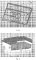
- FIG. 1 illustrates an example of the structure of an apparatus for use in cable television (CATV) network according to an embodiment.
- the apparatus 100 comprises a housing 102, a printed circuit board (PCB) 104 comprising components necessary for operating the apparatus, wherein the PCB is arranged within the housing 102 and a detachable cover 106 for the housing.
- the apparatus further comprises a casted covering plate 108 made of electrically conducting material, wherein the covering plate 108 is arranged, upon installation between the PCB 104 and the detachable cover 106, to cover at least the PCB and attach the PCB to the housing.
- a casted covering plate 108 made of electrically conducting material
- the protection functionalities both electrical and mechanical, can be achieved by a single casted covering plate.
- the casted covering plate alone would provide an improved RF protection, even without the detachable cover.
- the PCB instead of fastening the PCB to the housing using typically at least ten manually fastened screws, the PCB can be attached firmly to the housing by an appropriately designed casted covering plate. Since no screw holes are needed in the PCB, there is more space on the PCB for further components.
- the covering plate alone provides a sufficient RF protection, the covering plate could be even used as the outer cover of the apparatus instead of the detachable cover. At least the detachable cover could be made of plastic, for example, instead of aluminium, thereby proving savings in material and manufacturing costs.
- the covering plate comprises at least one aperture 110, 112, 114, 116 for a test point 118 of the apparatus or arranged as a guide for a plug-in module 120, 122.
- the apertures in the covering plate can be designed such that they operate as guides.
- the detachable cover can be removed for maintenance or testing purposes without the fear that another RF device, such as cellular network base station, operating in the vicinity of apparatus would cause RF interference to the apparatus.
- another RF device such as cellular network base station
- an old, broken or non-optimal plug-in module can be replaced by a new plug-in module, or a testing apparatus can be connected to the test point for monitoring the operation of the apparatus without causing RF interference to the apparatus.
- a second surface of the covering plate facing the PCB is casted in a form that provides isolation walls and/or a shielding box around at least one component or a component group on the PCB.
- Figure 2 illustrates an example of the structure of the covering plate 108 on the surface facing the PCB.
- the structure of the apertures 110, 112, 114 arranged as guides for plug-in modules, as shown in Figure 1 is shown more clearly in Figure 2 .
- the walls of the apertures extend upfront from the surface, thus providing a firm and solid guide to install and remove plug-in modules.
- the aperture 116 for the test point does not require a guide because the test point 118 is fixed to the PCB.
- Figure 2 further shows casted walls 126, 128 and a shielding box 130, which upon installing the covering plate on the PCB, provide RF isolation for one components or component groups that they surround.
- the design of the covering plate is such that the outer edges 132 and/or the walls 126, 128 and the shielding box 130 press the PCB firmly to its place, and provide electrical contact between the PCB and the housing of the apparatus such that the PCB is securely connected to the ground potential of the housing.
- the outer surfaces of the edges 132 may be covered with an electrically conducting material, such as electrically conducting foam or a plait gasket.
- the electrically conducting material is aluminium, zinc or an electrically conducting plastic.
- an electrically conducting plastic could be used instead.
- the covering plate is attached to the housing by one screw.
- the fastening may be carried out using a screw 124 extending preferably through the PCB 104 to the bottom of the housing 102.
- a screw 124 extending preferably through the PCB 104 to the bottom of the housing 102.
- fastening screws may be carried out using several, such as 2, 3 or 4, fastening screws.
- alternative means for fastening the covering plate may be used, such as one or more springs exerting spring force between the housing and the covering plate, a separate fastening part between the housing and the covering plate, pressing the covering plate to its position, etc.
- Figure 3 illustrates an example of the structure of an apparatus, when the parts have been installed together.
- the covering plate according to the embodiments provides a distinct, straightforward and easy-to-assemble solution for attaching the PCB to the housing of the apparatus, wherein the number of fastening screws is minimized, and the design of the covering plate is casted such that it replaces the required number of shielding boxes and partition walls as well as guides for plug-in modules.
- the number of separate parts, such as screws, shielding covers, mounting towers, shielding boxes and partition walls, in the apparatus reduces dramatically and assembly becomes easier. As a result, the assembly time of the apparatus in the manufacturing can be reduced to 1/10 or even further compared to prior art apparatuses.
- test point 118 is implemented as a component assembled on the PCB and extending upwards from the PCB such that the test point connector extends through the aperture 116 in the covering plate.
- the test point component needs to be typically assembled manually as a THT (Through-Hole-Technology) assembly on the PCB.
- a test point connector is arranged in a first surface of the covering plate facing the detachable cover, and a conductor connected to the test point connector and protruding from the second opposite surface of the covering plate, wherein the conductor, upon said installation of the covering plate, is arranged to be pressed against an output of a test signal on the PCB.
- the test point connector is implemented in the covering plate, and there is a rigid, elongated conductor on the opposite side of the covering plate.
- the output of the test signal may be implemented, for example, as a conducting spring.
- the length of the conductor is arranged such that when the covering plate is installed on the PCB, the conductor extends to the output of the test signal, and for example, presses against the conducting spring such that the test signal may be conducted to the test point connector. Consequently, the number of manually THT-assembled components on the PCB can be further reduced, which shortens the assembly time of the apparatus.
- Figure 4a shows the covering plate 108 as installed to its place within the housing 102.
- the sectional view shown in Figure 4b illustrates the structure of the test point more in detail.
- the test point comprises the test point connector 118a, the conductor 118b and the output of the test signal 118c, in this case a conducting spring, on the PCB 104.
- the test point connector 118a extends from the first (upper) surface of the covering plate 108.
- a rigid, elongated conductor 118b is arranged on the opposite side of the covering plate.
- the conductor 118b extends to the output of the test signal 118c.
- the head of the conductor 118b presses against the conducting spring such that there is an electrical contact between the test point connector 118a and the output of the test signal 118c.
Landscapes
- Engineering & Computer Science (AREA)
- Signal Processing (AREA)
- Microelectronics & Electronic Packaging (AREA)
- Shielding Devices Or Components To Electric Or Magnetic Fields (AREA)
Description
- The present invention relates to CATV networks, and more particularly to a structure of a CATV field device.
- Cable television (CATV) networks may be implemented with various techniques and network topologies, but currently most cable television networks are implemented as so-called HFC networks (Hybrid Fiber Coax), i.e. as combinations of a fibre network and a coaxial cable network. The distribution network for distributing the services from the main amplifier (a so-called headend) to the customers comprises a plurality of so-called field devices, such as fibre nodes, broadband amplifiers, etc.
- The HFC field devices are typically implemented in a casted aluminium housing so as to provide a robust and secure, yet a lightweight structure. Casted aluminium HFC field devices usually have a plurality of shielding covers to protect the printed circuit board (PCB) and the components. Several materials are used for this purpose: paper, plastic, metal. Metallic shielding covers are typically secured to a right place and on a right height from the PCB by using mounting towers protruding from the PCB, to which towers the shielding covers are attached. The PCBs are attached to mechanics (i.e. the casted housing) with screws to make a good and reliable contact.
- In many occasions, metallic shielding covers are mandatory due to their electromagnetic compatibility (EMC) properties, since the HFC devices have conducting surface above and below the PCB. Some components and power sources must typically be isolated for EMC reasons by additional sheet metal walls and shielding boxes. The high-voltage power sources must also be covered by shielding covers due to safety reasons.
- Typically at least some of the components or functionalities in HFC field devices are implemented as plug-in components, or more generally as plug-in modules, so as to enable easy replacement of a broken or an outdated module. Also when configuring the network, the plug-in modules may be switched several times when aiming to optimize the operation of the field device in terms of the whole network configuration. The plug-in modules usually need a plastic or metallic guide to secure correct installation. The guide may be attached to the shielding cover or it may be a separate part.
- However, the separate parts mentioned above, such as screws, shielding covers, mounting towers, shielding boxes and partition walls, typically need to be assembled manually on the PCB or in the housing. This causes additional manual work and delays in the manufacturing and the assembly time of a single apparatus becomes unnecessarily long. Moreover, most of the above-mentioned parts are installed on the PCB, thereby requiring space for installation, which in turn limits the number of components installable on the PCB.
- Yet a further problem may occur in a situation, where the apparatus is operated in the CATV network and there is another RF device, such as cellular network base station, operating in the vicinity of apparatus. The cover or the cap of the apparatus typically provides sufficient protection against RF interference from other RF devices and disturbances from other sources. However, no maintenance or testing of the apparatus can be made without removing or opening the cover, which in turn would cause RF interference to the apparatus. As a result, the apparatus does not work properly, and it might even damage. Therefore, no reliable testing results can be achieved, and for the maintenance work, the apparatus practically needs to be shut down, thereby causing a breakdown in the service.
-
US 2005/227744 discloses a radio frequency (RF) tuner includes a tuner housing, a cover coupled to a first side of the housing, and a tuner printed circuit board (PCB) including a plurality of layers coupled to a second side of the housing, wherein the layers are configured to shield the tuner PCB thereby reducing electromagnetic interference emissions and RF radiated fields in said PCB. -
WO 2012/122230 discloses a set top box comprising a bottom frame; a top cover; a printed circuit board positioned between the bottom frame and the top cover; and a top heat sink that completely covers or substantially covers the printed circuit board. The top heat sink comprises an access aperture for providing access to a reset point on the printed circuit board. - Now there has been invented an improved apparatus, by which many of the above problems can be removed or at least alleviated. Herein below a field device of a CATV network is introduced, which is characterized by what is stated in the independent claim. Various embodiments of the invention are disclosed in the dependent claims. The scope of protection sought for various embodiments of the invention is set out by the independent claims. The embodiments and features, if any, described in this specification that do not fall under the scope of the independent claims are to be interpreted as examples useful for understanding various embodiments of the invention.
- According to an aspect, there is provided an apparatus for use in cable television (CATV) network, the apparatus comprising: a housing; a printed circuit board (PCB) comprising components necessary for operating the apparatus, wherein the PCB is arranged within the housing; a detachable cover for the housing; and a casted covering plate made of electrically conducting material, wherein the covering plate is arranged, upon installation between the PCB and the detachable cover, to cover at least the PCB and attach the PCB to the housing, wherein the covering plate comprises at least one aperture for a test point of the apparatus or arranged as a guide for a plug-in module; and a test point connector is arranged in a first surface of the covering plate facing the detachable cover, and a conductor connected to the test point connector and protruding from the second opposite surface of the covering plate, wherein the conductor, upon said installation of the covering plate, is arranged to be pressed against an output of a test signal on the PCB.
- According to an embodiment, a second surface of the covering plate facing the PCB is casted in a form that provides isolation walls and/or a shielding box around at least one component or a component group on the PCB.
- According to an embodiment, the electrically conducting material is aluminium, zinc or an electrically conducting plastic.
- According to an embodiment, the covering plate is attached to the housing by one screw.
- These and other aspects of the invention and the embodiments related thereto will become apparent in view of the detailed disclosure of the embodiments further below.
- In the following, various embodiments of the invention will be described in more detail with reference to the appended drawings, in which
- Fig. 1
- shows an example of the structure of an apparatus according to an embodiment of the invention with several parts separated from each other;
- Fig. 2
- shows an example of the surface structure of a covering plate according to an embodiment of the invention;
- Fig. 3
- shows an example of the structure of an apparatus according to an embodiment of the invention with the parts installed together; and
- Figs 4a, 4b
- show an example of test point arrangement according to an embodiment of the invention.
-
Figure 1 illustrates an example of the structure of an apparatus for use in cable television (CATV) network according to an embodiment. Theapparatus 100 comprises ahousing 102, a printed circuit board (PCB) 104 comprising components necessary for operating the apparatus, wherein the PCB is arranged within thehousing 102 and adetachable cover 106 for the housing. The apparatus further comprises a castedcovering plate 108 made of electrically conducting material, wherein thecovering plate 108 is arranged, upon installation between thePCB 104 and thedetachable cover 106, to cover at least the PCB and attach the PCB to the housing. - Thus, instead of using a plurality of shielding covers to protect the PCB and the components, the protection functionalities, both electrical and mechanical, can be achieved by a single casted covering plate. Regarding possible RF interference from other RF devices in the vicinity, the casted covering plate alone would provide an improved RF protection, even without the detachable cover. Moreover, instead of fastening the PCB to the housing using typically at least ten manually fastened screws, the PCB can be attached firmly to the housing by an appropriately designed casted covering plate. Since no screw holes are needed in the PCB, there is more space on the PCB for further components.
- If the covering plate alone provides a sufficient RF protection, the covering plate could be even used as the outer cover of the apparatus instead of the detachable cover. At least the detachable cover could be made of plastic, for example, instead of aluminium, thereby proving savings in material and manufacturing costs.
- According to an embodiment, the covering plate comprises at least one
aperture test point 118 of the apparatus or arranged as a guide for a plug-in module 120, 122. Hence, no separate guides are needed for plug-ins, but the apertures in the covering plate can be designed such that they operate as guides. - This provides the further advantage that the detachable cover can be removed for maintenance or testing purposes without the fear that another RF device, such as cellular network base station, operating in the vicinity of apparatus would cause RF interference to the apparatus. Thus, an old, broken or non-optimal plug-in module can be replaced by a new plug-in module, or a testing apparatus can be connected to the test point for monitoring the operation of the apparatus without causing RF interference to the apparatus.
- According to an embodiment, a second surface of the covering plate facing the PCB is casted in a form that provides isolation walls and/or a shielding box around at least one component or a component group on the PCB.
-
Figure 2 illustrates an example of the structure of thecovering plate 108 on the surface facing the PCB. The structure of theapertures Figure 1 , is shown more clearly inFigure 2 . The walls of the apertures extend upfront from the surface, thus providing a firm and solid guide to install and remove plug-in modules. Theaperture 116 for the test point does not require a guide because thetest point 118 is fixed to the PCB.Figure 2 further shows castedwalls - The design of the covering plate is such that the
outer edges 132 and/or thewalls edges 132 may be covered with an electrically conducting material, such as electrically conducting foam or a plait gasket. - According to an embodiment, the electrically conducting material is aluminium, zinc or an electrically conducting plastic. When selecting an appropriate material for the covering plate, in addition to the electrical conducting properties, also the castability and manufacturing costs play an important role. Therefore, regarding metals aluminium (Al) or zinc (Zn) are preferable materials. Alternatively, an electrically conducting plastic could be used instead.
- According to an embodiment, the covering plate is attached to the housing by one screw. Depending on the location and the orientation of the apparatus as installed in the network, it may be preferable to ensure secure fastening of the
covering plate 108 to thePCB 104 and/or thehousing 102. This is preferable at least when the apparatus is installed in vertical or upside down orientation or in a location where the apparatus may be subjected to vibration. - Referring back to
Figure 1 , the fastening may be carried out using a screw 124 extending preferably through thePCB 104 to the bottom of thehousing 102. A skilled person appreciates that while the aim is to keep the number of fastening screws as few as possible, preferably zero, in certain cases, depending e.g. on the size of the apparatus and the covering plate, it may be preferable to use several, such as 2, 3 or 4, fastening screws. On the other hand, alternative means for fastening the covering plate may be used, such as one or more springs exerting spring force between the housing and the covering plate, a separate fastening part between the housing and the covering plate, pressing the covering plate to its position, etc. -
Figure 3 illustrates an example of the structure of an apparatus, when the parts have been installed together. Compared to prior art solutions, the covering plate according to the embodiments provides a distinct, straightforward and easy-to-assemble solution for attaching the PCB to the housing of the apparatus, wherein the number of fastening screws is minimized, and the design of the covering plate is casted such that it replaces the required number of shielding boxes and partition walls as well as guides for plug-in modules. The number of separate parts, such as screws, shielding covers, mounting towers, shielding boxes and partition walls, in the apparatus reduces dramatically and assembly becomes easier. As a result, the assembly time of the apparatus in the manufacturing can be reduced to 1/10 or even further compared to prior art apparatuses. - In the above embodiments, the
test point 118 is implemented as a component assembled on the PCB and extending upwards from the PCB such that the test point connector extends through theaperture 116 in the covering plate. The test point component needs to be typically assembled manually as a THT (Through-Hole-Technology) assembly on the PCB. - According to an alternative embodiment, a test point connector is arranged in a first surface of the covering plate facing the detachable cover, and a conductor connected to the test point connector and protruding from the second opposite surface of the covering plate, wherein the conductor, upon said installation of the covering plate, is arranged to be pressed against an output of a test signal on the PCB.
- Accordingly, the test point connector is implemented in the covering plate, and there is a rigid, elongated conductor on the opposite side of the covering plate. On the PCB, the output of the test signal may be implemented, for example, as a conducting spring. The length of the conductor is arranged such that when the covering plate is installed on the PCB, the conductor extends to the output of the test signal, and for example, presses against the conducting spring such that the test signal may be conducted to the test point connector. Consequently, the number of manually THT-assembled components on the PCB can be further reduced, which shortens the assembly time of the apparatus.
- The embodiment is illustrated more in detail in
Figures 4a and 4b. Figure 4a shows thecovering plate 108 as installed to its place within thehousing 102. There are twotest points 118, or actually test point connectors, arranged on the surface of thecovering plate 108. - The sectional view shown in
Figure 4b illustrates the structure of the test point more in detail. The test point comprises the test point connector 118a, theconductor 118b and the output of thetest signal 118c, in this case a conducting spring, on thePCB 104. The test point connector 118a extends from the first (upper) surface of thecovering plate 108. A rigid,elongated conductor 118b is arranged on the opposite side of the covering plate. When thecovering plate 108 is installed within thehousing 102 and on thePCB 104, theconductor 118b extends to the output of thetest signal 118c. The head of theconductor 118b presses against the conducting spring such that there is an electrical contact between the test point connector 118a and the output of thetest signal 118c. - A skilled man appreciates that any of the embodiments described above may be implemented as a combination with one or more of the other embodiments, unless there is explicitly or implicitly stated that certain embodiments are only alternatives to each other.
- It is obvious that the present invention is not limited solely to the above-presented embodiments, but it can be modified within the scope of the appended claims.
Claims (4)
- An apparatus for use in cable television (CATV) network, the apparatus comprising:a housing (102);a printed circuit board (PCB; 104) comprising components necessary for operating the apparatus, wherein the PCB (104) is arranged within the housing (102);a detachable cover (106) for the housing;a casted covering plate (108) made of electrically conducting material, wherein the covering plate (108) is arranged, upon installation between the PCB (104) and the detachable cover (106), to cover at least the PCB and attach the PCB to the housing; whereinthe covering plate (108) comprises at least one aperture (110, 112, 114, 116) for a test point (118) of the apparatus or arranged as a guide for a plug-in module (120, 122); anda test point connector (118a) is arranged in a first surface of the covering plate (108) facing the detachable cover (106), and a conductor (118b) connected to the test point connector (118a) and protruding from the second opposite surface of the covering plate (108), wherein the conductor (118b), upon said installation of the covering plate (108), is arranged to be pressed against an output of a test signal (118c) on the PCB (104).
- The apparatus according to claim 1, wherein a second surface of the covering plate (108) facing the PCB (104) is casted in a form that provides isolation walls (126, 128) and/or a shielding box (130) around at least one component or a component group on the PCB.
- The apparatus according to claim 1 or 2, wherein the electrically conducting material is aluminium, zinc or an electrically conducting plastic.
- The apparatus according to any preceding claim, wherein the covering plate (108) is attached to the housing (102) by one screw (124) .
Applications Claiming Priority (1)
| Application Number | Priority Date | Filing Date | Title |
|---|---|---|---|
| PCT/FI2016/050273 WO2017187004A1 (en) | 2016-04-28 | 2016-04-28 | Structural arrangement for a catv field device |
Publications (3)
| Publication Number | Publication Date |
|---|---|
| EP3449706A1 EP3449706A1 (en) | 2019-03-06 |
| EP3449706A4 EP3449706A4 (en) | 2020-01-01 |
| EP3449706B1 true EP3449706B1 (en) | 2021-02-17 |
Family
ID=60160163
Family Applications (1)
| Application Number | Title | Priority Date | Filing Date |
|---|---|---|---|
| EP16900320.9A Active EP3449706B1 (en) | 2016-04-28 | 2016-04-28 | Structural arrangement for a catv field device |
Country Status (4)
| Country | Link |
|---|---|
| EP (1) | EP3449706B1 (en) |
| DK (1) | DK3449706T3 (en) |
| ES (1) | ES2863777T3 (en) |
| WO (1) | WO2017187004A1 (en) |
Cited By (1)
| Publication number | Priority date | Publication date | Assignee | Title |
|---|---|---|---|---|
| DE102022104810A1 (en) | 2022-03-01 | 2023-09-07 | HELLA GmbH & Co. KGaA | Housing, in particular for a control device, with shielding against electromagnetic radiation |
Family Cites Families (8)
| Publication number | Priority date | Publication date | Assignee | Title |
|---|---|---|---|---|
| WO2001099483A1 (en) * | 2000-06-20 | 2001-12-27 | Laird Technologies, Inc. | Shielding cover with integral resilient ribs |
| JP2002368360A (en) * | 2001-06-12 | 2002-12-20 | Nec Corp | Circuit board provided with protection cover |
| US20050227744A1 (en) * | 2004-04-08 | 2005-10-13 | Yen-Fu Chiang | System and method for a simplified cable tuner |
| JP2006060474A (en) * | 2004-08-19 | 2006-03-02 | Toshiba Corp | Cable modem module device, cable modem device and broadcasting receiver |
| EP2684375B8 (en) | 2011-03-09 | 2017-12-13 | Thomson Licensing | Set top box or server having snap-in heat sink and smart card reader |
| US9179538B2 (en) * | 2011-06-09 | 2015-11-03 | Apple Inc. | Electromagnetic shielding structures for selectively shielding components on a substrate |
| US9007773B2 (en) * | 2012-08-31 | 2015-04-14 | Flextronics Ap, Llc | Housing unit with heat sink |
| JP6186143B2 (en) * | 2013-03-13 | 2017-08-23 | 日立オートモティブシステムズ株式会社 | Power converter |
-
2016
- 2016-04-28 WO PCT/FI2016/050273 patent/WO2017187004A1/en active Application Filing
- 2016-04-28 DK DK16900320.9T patent/DK3449706T3/en active
- 2016-04-28 EP EP16900320.9A patent/EP3449706B1/en active Active
- 2016-04-28 ES ES16900320T patent/ES2863777T3/en active Active
Non-Patent Citations (1)
| Title |
|---|
| None * |
Cited By (1)
| Publication number | Priority date | Publication date | Assignee | Title |
|---|---|---|---|---|
| DE102022104810A1 (en) | 2022-03-01 | 2023-09-07 | HELLA GmbH & Co. KGaA | Housing, in particular for a control device, with shielding against electromagnetic radiation |
Also Published As
| Publication number | Publication date |
|---|---|
| WO2017187004A1 (en) | 2017-11-02 |
| EP3449706A4 (en) | 2020-01-01 |
| EP3449706A1 (en) | 2019-03-06 |
| DK3449706T3 (en) | 2021-05-10 |
| ES2863777T3 (en) | 2021-10-11 |
Similar Documents
| Publication | Publication Date | Title |
|---|---|---|
| US20030218873A1 (en) | Structure for fastening a component | |
| US9661791B2 (en) | RF interference suppressor | |
| US5748449A (en) | Electrical enclosure for radio | |
| US7868258B2 (en) | Radio frequency module assembly | |
| US9620940B2 (en) | Medium voltage switchgear with front accessibility of current transformers mounted external to a rear of a circuit breaker compartment | |
| EP3449706B1 (en) | Structural arrangement for a catv field device | |
| KR102483262B1 (en) | Shield can device for blocking electromagnetic wave | |
| CN101355867B (en) | Shielding device | |
| JP4731788B2 (en) | Cable wiring structure and electronic device having cable wiring structure | |
| CN111527801B (en) | Cable seal assembly | |
| US8861209B2 (en) | Electromagnetic shield | |
| US20220248575A1 (en) | Electronic control device | |
| KR102425986B1 (en) | Electrical system with shielding | |
| US20220418136A1 (en) | Housing for railroad switch | |
| KR100984158B1 (en) | Set-top-box with common type shield case | |
| JP2006210742A (en) | Shield case for electronic equipment and eletronic equipment | |
| KR101933407B1 (en) | Radio communication module | |
| US20100238641A1 (en) | Shield structure of a tuner apparatus | |
| EP2641459B1 (en) | An electronics device, and a method for making the same | |
| US20150002358A1 (en) | Radio communication module | |
| EP2887453A1 (en) | Radio communication module | |
| US11289792B2 (en) | Communication device comprising a mounting structure and valve unit | |
| US8477513B2 (en) | Electrical connector shield | |
| US20130265675A1 (en) | Digital protective relay | |
| US20150077925A1 (en) | Set top box having removable hard drive |
Legal Events
| Date | Code | Title | Description |
|---|---|---|---|
| STAA | Information on the status of an ep patent application or granted ep patent |
Free format text: STATUS: THE INTERNATIONAL PUBLICATION HAS BEEN MADE |
|
| PUAI | Public reference made under article 153(3) epc to a published international application that has entered the european phase |
Free format text: ORIGINAL CODE: 0009012 |
|
| STAA | Information on the status of an ep patent application or granted ep patent |
Free format text: STATUS: REQUEST FOR EXAMINATION WAS MADE |
|
| 17P | Request for examination filed |
Effective date: 20181022 |
|
| AK | Designated contracting states |
Kind code of ref document: A1 Designated state(s): AL AT BE BG CH CY CZ DE DK EE ES FI FR GB GR HR HU IE IS IT LI LT LU LV MC MK MT NL NO PL PT RO RS SE SI SK SM TR |
|
| AX | Request for extension of the european patent |
Extension state: BA ME |
|
| DAV | Request for validation of the european patent (deleted) | ||
| DAX | Request for extension of the european patent (deleted) | ||
| A4 | Supplementary search report drawn up and despatched |
Effective date: 20191204 |
|
| RIC1 | Information provided on ipc code assigned before grant |
Ipc: H04N 7/10 20060101ALI20191128BHEP Ipc: H05K 9/00 20060101ALI20191128BHEP Ipc: H04H 20/78 20080101ALI20191128BHEP Ipc: H05K 5/03 20060101AFI20191128BHEP Ipc: H05K 5/04 20060101ALI20191128BHEP |
|
| GRAP | Despatch of communication of intention to grant a patent |
Free format text: ORIGINAL CODE: EPIDOSNIGR1 |
|
| STAA | Information on the status of an ep patent application or granted ep patent |
Free format text: STATUS: GRANT OF PATENT IS INTENDED |
|
| INTG | Intention to grant announced |
Effective date: 20200916 |
|
| GRAS | Grant fee paid |
Free format text: ORIGINAL CODE: EPIDOSNIGR3 |
|
| GRAA | (expected) grant |
Free format text: ORIGINAL CODE: 0009210 |
|
| STAA | Information on the status of an ep patent application or granted ep patent |
Free format text: STATUS: THE PATENT HAS BEEN GRANTED |
|
| AK | Designated contracting states |
Kind code of ref document: B1 Designated state(s): AL AT BE BG CH CY CZ DE DK EE ES FI FR GB GR HR HU IE IS IT LI LT LU LV MC MK MT NL NO PL PT RO RS SE SI SK SM TR |
|
| REG | Reference to a national code |
Ref country code: GB Ref legal event code: FG4D |
|
| REG | Reference to a national code |
Ref country code: CH Ref legal event code: EP |
|
| REG | Reference to a national code |
Ref country code: DE Ref legal event code: R096 Ref document number: 602016052904 Country of ref document: DE |
|
| REG | Reference to a national code |
Ref country code: AT Ref legal event code: REF Ref document number: 1363264 Country of ref document: AT Kind code of ref document: T Effective date: 20210315 |
|
| REG | Reference to a national code |
Ref country code: IE Ref legal event code: FG4D |
|
| REG | Reference to a national code |
Ref country code: SE Ref legal event code: TRGR |
|
| REG | Reference to a national code |
Ref country code: NL Ref legal event code: FP |
|
| REG | Reference to a national code |
Ref country code: FI Ref legal event code: FGE |
|
| REG | Reference to a national code |
Ref country code: DK Ref legal event code: T3 Effective date: 20210506 |
|
| REG | Reference to a national code |
Ref country code: LT Ref legal event code: MG9D |
|
| REG | Reference to a national code |
Ref country code: NO Ref legal event code: T2 Effective date: 20210217 |
|
| PG25 | Lapsed in a contracting state [announced via postgrant information from national office to epo] |
Ref country code: HR Free format text: LAPSE BECAUSE OF FAILURE TO SUBMIT A TRANSLATION OF THE DESCRIPTION OR TO PAY THE FEE WITHIN THE PRESCRIBED TIME-LIMIT Effective date: 20210217 Ref country code: GR Free format text: LAPSE BECAUSE OF FAILURE TO SUBMIT A TRANSLATION OF THE DESCRIPTION OR TO PAY THE FEE WITHIN THE PRESCRIBED TIME-LIMIT Effective date: 20210518 Ref country code: PT Free format text: LAPSE BECAUSE OF FAILURE TO SUBMIT A TRANSLATION OF THE DESCRIPTION OR TO PAY THE FEE WITHIN THE PRESCRIBED TIME-LIMIT Effective date: 20210617 Ref country code: BG Free format text: LAPSE BECAUSE OF FAILURE TO SUBMIT A TRANSLATION OF THE DESCRIPTION OR TO PAY THE FEE WITHIN THE PRESCRIBED TIME-LIMIT Effective date: 20210517 Ref country code: LT Free format text: LAPSE BECAUSE OF FAILURE TO SUBMIT A TRANSLATION OF THE DESCRIPTION OR TO PAY THE FEE WITHIN THE PRESCRIBED TIME-LIMIT Effective date: 20210217 |
|
| REG | Reference to a national code |
Ref country code: AT Ref legal event code: MK05 Ref document number: 1363264 Country of ref document: AT Kind code of ref document: T Effective date: 20210217 |
|
| PG25 | Lapsed in a contracting state [announced via postgrant information from national office to epo] |
Ref country code: PL Free format text: LAPSE BECAUSE OF FAILURE TO SUBMIT A TRANSLATION OF THE DESCRIPTION OR TO PAY THE FEE WITHIN THE PRESCRIBED TIME-LIMIT Effective date: 20210217 Ref country code: LV Free format text: LAPSE BECAUSE OF FAILURE TO SUBMIT A TRANSLATION OF THE DESCRIPTION OR TO PAY THE FEE WITHIN THE PRESCRIBED TIME-LIMIT Effective date: 20210217 Ref country code: RS Free format text: LAPSE BECAUSE OF FAILURE TO SUBMIT A TRANSLATION OF THE DESCRIPTION OR TO PAY THE FEE WITHIN THE PRESCRIBED TIME-LIMIT Effective date: 20210217 |
|
| PG25 | Lapsed in a contracting state [announced via postgrant information from national office to epo] |
Ref country code: IS Free format text: LAPSE BECAUSE OF FAILURE TO SUBMIT A TRANSLATION OF THE DESCRIPTION OR TO PAY THE FEE WITHIN THE PRESCRIBED TIME-LIMIT Effective date: 20210617 |
|
| REG | Reference to a national code |
Ref country code: ES Ref legal event code: FG2A Ref document number: 2863777 Country of ref document: ES Kind code of ref document: T3 Effective date: 20211011 |
|
| PG25 | Lapsed in a contracting state [announced via postgrant information from national office to epo] |
Ref country code: EE Free format text: LAPSE BECAUSE OF FAILURE TO SUBMIT A TRANSLATION OF THE DESCRIPTION OR TO PAY THE FEE WITHIN THE PRESCRIBED TIME-LIMIT Effective date: 20210217 Ref country code: CZ Free format text: LAPSE BECAUSE OF FAILURE TO SUBMIT A TRANSLATION OF THE DESCRIPTION OR TO PAY THE FEE WITHIN THE PRESCRIBED TIME-LIMIT Effective date: 20210217 Ref country code: SM Free format text: LAPSE BECAUSE OF FAILURE TO SUBMIT A TRANSLATION OF THE DESCRIPTION OR TO PAY THE FEE WITHIN THE PRESCRIBED TIME-LIMIT Effective date: 20210217 Ref country code: AT Free format text: LAPSE BECAUSE OF FAILURE TO SUBMIT A TRANSLATION OF THE DESCRIPTION OR TO PAY THE FEE WITHIN THE PRESCRIBED TIME-LIMIT Effective date: 20210217 |
|
| REG | Reference to a national code |
Ref country code: DE Ref legal event code: R119 Ref document number: 602016052904 Country of ref document: DE |
|
| PG25 | Lapsed in a contracting state [announced via postgrant information from national office to epo] |
Ref country code: SK Free format text: LAPSE BECAUSE OF FAILURE TO SUBMIT A TRANSLATION OF THE DESCRIPTION OR TO PAY THE FEE WITHIN THE PRESCRIBED TIME-LIMIT Effective date: 20210217 Ref country code: RO Free format text: LAPSE BECAUSE OF FAILURE TO SUBMIT A TRANSLATION OF THE DESCRIPTION OR TO PAY THE FEE WITHIN THE PRESCRIBED TIME-LIMIT Effective date: 20210217 Ref country code: MC Free format text: LAPSE BECAUSE OF FAILURE TO SUBMIT A TRANSLATION OF THE DESCRIPTION OR TO PAY THE FEE WITHIN THE PRESCRIBED TIME-LIMIT Effective date: 20210217 |
|
| PLBE | No opposition filed within time limit |
Free format text: ORIGINAL CODE: 0009261 |
|
| STAA | Information on the status of an ep patent application or granted ep patent |
Free format text: STATUS: NO OPPOSITION FILED WITHIN TIME LIMIT |
|
| PG25 | Lapsed in a contracting state [announced via postgrant information from national office to epo] |
Ref country code: LU Free format text: LAPSE BECAUSE OF NON-PAYMENT OF DUE FEES Effective date: 20210428 |
|
| 26N | No opposition filed |
Effective date: 20211118 |
|
| PG25 | Lapsed in a contracting state [announced via postgrant information from national office to epo] |
Ref country code: DE Free format text: LAPSE BECAUSE OF NON-PAYMENT OF DUE FEES Effective date: 20211103 Ref country code: AL Free format text: LAPSE BECAUSE OF FAILURE TO SUBMIT A TRANSLATION OF THE DESCRIPTION OR TO PAY THE FEE WITHIN THE PRESCRIBED TIME-LIMIT Effective date: 20210217 |
|
| PG25 | Lapsed in a contracting state [announced via postgrant information from national office to epo] |
Ref country code: SI Free format text: LAPSE BECAUSE OF FAILURE TO SUBMIT A TRANSLATION OF THE DESCRIPTION OR TO PAY THE FEE WITHIN THE PRESCRIBED TIME-LIMIT Effective date: 20210217 |
|
| PG25 | Lapsed in a contracting state [announced via postgrant information from national office to epo] |
Ref country code: IT Free format text: LAPSE BECAUSE OF FAILURE TO SUBMIT A TRANSLATION OF THE DESCRIPTION OR TO PAY THE FEE WITHIN THE PRESCRIBED TIME-LIMIT Effective date: 20210217 Ref country code: IE Free format text: LAPSE BECAUSE OF NON-PAYMENT OF DUE FEES Effective date: 20210428 |
|
| PG25 | Lapsed in a contracting state [announced via postgrant information from national office to epo] |
Ref country code: IS Free format text: LAPSE BECAUSE OF FAILURE TO SUBMIT A TRANSLATION OF THE DESCRIPTION OR TO PAY THE FEE WITHIN THE PRESCRIBED TIME-LIMIT Effective date: 20210617 Ref country code: FR Free format text: LAPSE BECAUSE OF NON-PAYMENT OF DUE FEES Effective date: 20210430 |
|
| PGFP | Annual fee paid to national office [announced via postgrant information from national office to epo] |
Ref country code: NL Payment date: 20220420 Year of fee payment: 7 |
|
| PGFP | Annual fee paid to national office [announced via postgrant information from national office to epo] |
Ref country code: SE Payment date: 20220421 Year of fee payment: 7 Ref country code: NO Payment date: 20220425 Year of fee payment: 7 Ref country code: GB Payment date: 20220425 Year of fee payment: 7 Ref country code: ES Payment date: 20220629 Year of fee payment: 7 Ref country code: DK Payment date: 20220422 Year of fee payment: 7 |
|
| PGFP | Annual fee paid to national office [announced via postgrant information from national office to epo] |
Ref country code: FI Payment date: 20220421 Year of fee payment: 7 Ref country code: CH Payment date: 20220421 Year of fee payment: 7 Ref country code: BE Payment date: 20220421 Year of fee payment: 7 |
|
| PG25 | Lapsed in a contracting state [announced via postgrant information from national office to epo] |
Ref country code: CY Free format text: LAPSE BECAUSE OF FAILURE TO SUBMIT A TRANSLATION OF THE DESCRIPTION OR TO PAY THE FEE WITHIN THE PRESCRIBED TIME-LIMIT Effective date: 20210217 |
|
| PG25 | Lapsed in a contracting state [announced via postgrant information from national office to epo] |
Ref country code: HU Free format text: LAPSE BECAUSE OF FAILURE TO SUBMIT A TRANSLATION OF THE DESCRIPTION OR TO PAY THE FEE WITHIN THE PRESCRIBED TIME-LIMIT; INVALID AB INITIO Effective date: 20160428 |
|
| REG | Reference to a national code |
Ref country code: NO Ref legal event code: MMEP |
|
| REG | Reference to a national code |
Ref country code: DK Ref legal event code: EBP Effective date: 20230430 |
|
| REG | Reference to a national code |
Ref country code: SE Ref legal event code: EUG |
|
| REG | Reference to a national code |
Ref country code: CH Ref legal event code: PL |
|
| REG | Reference to a national code |
Ref country code: NL Ref legal event code: MM Effective date: 20230501 |
|
| GBPC | Gb: european patent ceased through non-payment of renewal fee |
Effective date: 20230428 |
|
| REG | Reference to a national code |
Ref country code: BE Ref legal event code: MM Effective date: 20230430 |
|
| PG25 | Lapsed in a contracting state [announced via postgrant information from national office to epo] |
Ref country code: GB Free format text: LAPSE BECAUSE OF NON-PAYMENT OF DUE FEES Effective date: 20230428 |
|
| PG25 | Lapsed in a contracting state [announced via postgrant information from national office to epo] |
Ref country code: SE Free format text: LAPSE BECAUSE OF NON-PAYMENT OF DUE FEES Effective date: 20230429 Ref country code: NO Free format text: LAPSE BECAUSE OF NON-PAYMENT OF DUE FEES Effective date: 20230430 Ref country code: NL Free format text: LAPSE BECAUSE OF NON-PAYMENT OF DUE FEES Effective date: 20230501 Ref country code: LI Free format text: LAPSE BECAUSE OF NON-PAYMENT OF DUE FEES Effective date: 20230430 Ref country code: GB Free format text: LAPSE BECAUSE OF NON-PAYMENT OF DUE FEES Effective date: 20230428 Ref country code: FI Free format text: LAPSE BECAUSE OF NON-PAYMENT OF DUE FEES Effective date: 20230428 Ref country code: CH Free format text: LAPSE BECAUSE OF NON-PAYMENT OF DUE FEES Effective date: 20230430 |
|
| PG25 | Lapsed in a contracting state [announced via postgrant information from national office to epo] |
Ref country code: BE Free format text: LAPSE BECAUSE OF NON-PAYMENT OF DUE FEES Effective date: 20230430 |
|
| PG25 | Lapsed in a contracting state [announced via postgrant information from national office to epo] |
Ref country code: MK Free format text: LAPSE BECAUSE OF FAILURE TO SUBMIT A TRANSLATION OF THE DESCRIPTION OR TO PAY THE FEE WITHIN THE PRESCRIBED TIME-LIMIT Effective date: 20210217 Ref country code: DK Free format text: LAPSE BECAUSE OF NON-PAYMENT OF DUE FEES Effective date: 20230430 |
|
| REG | Reference to a national code |
Ref country code: ES Ref legal event code: FD2A Effective date: 20240531 |
|
| PG25 | Lapsed in a contracting state [announced via postgrant information from national office to epo] |
Ref country code: TR Free format text: LAPSE BECAUSE OF FAILURE TO SUBMIT A TRANSLATION OF THE DESCRIPTION OR TO PAY THE FEE WITHIN THE PRESCRIBED TIME-LIMIT Effective date: 20210217 |
|
| PG25 | Lapsed in a contracting state [announced via postgrant information from national office to epo] |
Ref country code: ES Free format text: LAPSE BECAUSE OF NON-PAYMENT OF DUE FEES Effective date: 20230429 |
|
| PG25 | Lapsed in a contracting state [announced via postgrant information from national office to epo] |
Ref country code: ES Free format text: LAPSE BECAUSE OF NON-PAYMENT OF DUE FEES Effective date: 20230429 |