EP3447923A1 - Sigma-delta modulator and associated system improving spectrum efficiency of wired interconnection - Google Patents
Sigma-delta modulator and associated system improving spectrum efficiency of wired interconnection Download PDFInfo
- Publication number
- EP3447923A1 EP3447923A1 EP18187020.5A EP18187020A EP3447923A1 EP 3447923 A1 EP3447923 A1 EP 3447923A1 EP 18187020 A EP18187020 A EP 18187020A EP 3447923 A1 EP3447923 A1 EP 3447923A1
- Authority
- EP
- European Patent Office
- Prior art keywords
- signal
- samples
- sdm
- circuit
- bandpass
- Prior art date
- Legal status (The legal status is an assumption and is not a legal conclusion. Google has not performed a legal analysis and makes no representation as to the accuracy of the status listed.)
- Granted
Links
Images


Classifications
-
- H—ELECTRICITY
- H03—ELECTRONIC CIRCUITRY
- H03M—CODING; DECODING; CODE CONVERSION IN GENERAL
- H03M7/00—Conversion of a code where information is represented by a given sequence or number of digits to a code where the same, similar or subset of information is represented by a different sequence or number of digits
- H03M7/30—Compression; Expansion; Suppression of unnecessary data, e.g. redundancy reduction
- H03M7/3002—Conversion to or from differential modulation
- H03M7/3004—Digital delta-sigma modulation
- H03M7/3015—Structural details of digital delta-sigma modulators
- H03M7/3017—Arrangements specific to bandpass modulators
-
- H—ELECTRICITY
- H04—ELECTRIC COMMUNICATION TECHNIQUE
- H04L—TRANSMISSION OF DIGITAL INFORMATION, e.g. TELEGRAPHIC COMMUNICATION
- H04L25/00—Baseband systems
- H04L25/38—Synchronous or start-stop systems, e.g. for Baudot code
- H04L25/40—Transmitting circuits; Receiving circuits
- H04L25/49—Transmitting circuits; Receiving circuits using code conversion at the transmitter; using predistortion; using insertion of idle bits for obtaining a desired frequency spectrum; using three or more amplitude levels ; Baseband coding techniques specific to data transmission systems
- H04L25/4902—Pulse width modulation; Pulse position modulation
-
- H—ELECTRICITY
- H03—ELECTRONIC CIRCUITRY
- H03M—CODING; DECODING; CODE CONVERSION IN GENERAL
- H03M3/00—Conversion of analogue values to or from differential modulation
- H03M3/30—Delta-sigma modulation
-
- H—ELECTRICITY
- H03—ELECTRONIC CIRCUITRY
- H03M—CODING; DECODING; CODE CONVERSION IN GENERAL
- H03M1/00—Analogue/digital conversion; Digital/analogue conversion
- H03M1/12—Analogue/digital converters
-
- H—ELECTRICITY
- H03—ELECTRONIC CIRCUITRY
- H03M—CODING; DECODING; CODE CONVERSION IN GENERAL
- H03M3/00—Conversion of analogue values to or from differential modulation
- H03M3/30—Delta-sigma modulation
- H03M3/322—Continuously compensating for, or preventing, undesired influence of physical parameters
- H03M3/324—Continuously compensating for, or preventing, undesired influence of physical parameters characterised by means or methods for compensating or preventing more than one type of error at a time, e.g. by synchronisation or using a ratiometric arrangement
- H03M3/344—Continuously compensating for, or preventing, undesired influence of physical parameters characterised by means or methods for compensating or preventing more than one type of error at a time, e.g. by synchronisation or using a ratiometric arrangement by filtering other than the noise-shaping inherent to delta-sigma modulators, e.g. anti-aliasing
-
- H—ELECTRICITY
- H03—ELECTRONIC CIRCUITRY
- H03M—CODING; DECODING; CODE CONVERSION IN GENERAL
- H03M3/00—Conversion of analogue values to or from differential modulation
- H03M3/30—Delta-sigma modulation
- H03M3/39—Structural details of delta-sigma modulators, e.g. incremental delta-sigma modulators
- H03M3/402—Arrangements specific to bandpass modulators
-
- H—ELECTRICITY
- H03—ELECTRONIC CIRCUITRY
- H03M—CODING; DECODING; CODE CONVERSION IN GENERAL
- H03M3/00—Conversion of analogue values to or from differential modulation
- H03M3/30—Delta-sigma modulation
- H03M3/39—Structural details of delta-sigma modulators, e.g. incremental delta-sigma modulators
- H03M3/436—Structural details of delta-sigma modulators, e.g. incremental delta-sigma modulators characterised by the order of the loop filter, e.g. error feedback type
- H03M3/456—Structural details of delta-sigma modulators, e.g. incremental delta-sigma modulators characterised by the order of the loop filter, e.g. error feedback type the modulator having a first order loop filter in the feedforward path
-
- H—ELECTRICITY
- H03—ELECTRONIC CIRCUITRY
- H03M—CODING; DECODING; CODE CONVERSION IN GENERAL
- H03M3/00—Conversion of analogue values to or from differential modulation
- H03M3/30—Delta-sigma modulation
- H03M3/458—Analogue/digital converters using delta-sigma modulation as an intermediate step
-
- H—ELECTRICITY
- H03—ELECTRONIC CIRCUITRY
- H03M—CODING; DECODING; CODE CONVERSION IN GENERAL
- H03M3/00—Conversion of analogue values to or from differential modulation
- H03M3/30—Delta-sigma modulation
- H03M3/50—Digital/analogue converters using delta-sigma modulation as an intermediate step
- H03M3/502—Details of the final digital/analogue conversion following the digital delta-sigma modulation
- H03M3/504—Details of the final digital/analogue conversion following the digital delta-sigma modulation the final digital/analogue converter being constituted by a finite impulse response [FIR] filter, i.e. FIRDAC
-
- H—ELECTRICITY
- H04—ELECTRIC COMMUNICATION TECHNIQUE
- H04B—TRANSMISSION
- H04B14/00—Transmission systems not characterised by the medium used for transmission
- H04B14/02—Transmission systems not characterised by the medium used for transmission characterised by the use of pulse modulation
- H04B14/06—Transmission systems not characterised by the medium used for transmission characterised by the use of pulse modulation using differential modulation, e.g. delta modulation
- H04B14/062—Transmission systems not characterised by the medium used for transmission characterised by the use of pulse modulation using differential modulation, e.g. delta modulation using delta modulation or one-bit differential modulation [1DPCM]
-
- H—ELECTRICITY
- H04—ELECTRIC COMMUNICATION TECHNIQUE
- H04H—BROADCAST COMMUNICATION
- H04H20/00—Arrangements for broadcast or for distribution combined with broadcast
- H04H20/65—Arrangements characterised by transmission systems for broadcast
- H04H20/76—Wired systems
-
- H—ELECTRICITY
- H03—ELECTRONIC CIRCUITRY
- H03M—CODING; DECODING; CODE CONVERSION IN GENERAL
- H03M3/00—Conversion of analogue values to or from differential modulation
- H03M3/30—Delta-sigma modulation
- H03M3/39—Structural details of delta-sigma modulators, e.g. incremental delta-sigma modulators
- H03M3/436—Structural details of delta-sigma modulators, e.g. incremental delta-sigma modulators characterised by the order of the loop filter, e.g. error feedback type
- H03M3/438—Structural details of delta-sigma modulators, e.g. incremental delta-sigma modulators characterised by the order of the loop filter, e.g. error feedback type the modulator having a higher order loop filter in the feedforward path
- H03M3/454—Structural details of delta-sigma modulators, e.g. incremental delta-sigma modulators characterised by the order of the loop filter, e.g. error feedback type the modulator having a higher order loop filter in the feedforward path with distributed feedback, i.e. with feedback paths from the quantiser output to more than one filter stage
-
- H—ELECTRICITY
- H03—ELECTRONIC CIRCUITRY
- H03M—CODING; DECODING; CODE CONVERSION IN GENERAL
- H03M3/00—Conversion of analogue values to or from differential modulation
- H03M3/30—Delta-sigma modulation
- H03M3/458—Analogue/digital converters using delta-sigma modulation as an intermediate step
- H03M3/466—Multiplexed conversion systems
- H03M3/472—Shared, i.e. using a single converter for multiple channels
Definitions
- the present invention relates to sigma-delta modulator (SDM) and associated system improving spectrum efficiency of wired interconnection, and more particularly, to SDM and associated system improving spectrum efficiency by shaping noise with a modified noise transfer function having a frequency-domain notch at a passband, which is therefore available for carrying additional bandpass signal(s) besides low-pass baseband signal(s).
- SDM sigma-delta modulator
- FIG. 1 illustrating a conventional spectrum arrangement for baseband signal(s) at a low-pass band.
- a sampling frequency fs of the signal(s) is usually set much higher than a Nyquist sampling frequency f_N of the signal(s).
- the spectrum therefore has a large vacancy, which extends from the low-pass band to an half of the sampling frequency (fs/2), not fully utilized.
- An objective of the invention is providing an SDM (e.g., 120 in FIG. 2 ) improving spectrum efficiency of wired interconnection.
- the SDM may comprise a main circuit (e.g., 121) and a noise shaping circuit (e.g., 122).
- the main circuit may be coupled to an aggregated signal (e.g., sa1), for transferring the aggregated signal by a signal transfer function (e.g., STF(z)).
- the noise shaping circuit may be coupled to the main circuit, for shaping noise away from a low-pass band (e.g., LB) by a modified noise transfer function (e.g., mNTF(z)), wherein a frequency response (e.g., 126) of the modified noise transfer function has a notch (e.g., 124) at a passband (e.g., PB), and the passband may not overlap with the low-pass band.
- a low-pass band e.g., LB
- a modified noise transfer function e.g., mNTF(z)
- a frequency response e.g., 126
- a passband e.g., PB
- the SDM may modulate the aggregated signal to a modulated signal (e.g., sb1 in FIG. 2 ), and a ratio (e.g., M) dividing a sampling frequency (e.g., fs) of the modulated signal by a frequency (e.g., fP) of the passband may substantially equal a multiplication of four.
- the frequency of the passband may substantially equal a quarter of the sampling frequency of the modulated signal.
- the SDM may be a multi-bit SDM modulating the aggregated signal to a modulated signal of multiple bits per sample.
- the frequency response of the modified noise transfer function may further have a second notch (e.g., 125) at a high-pass band (e.g., HB), and the high-pass band may not overlap with the passband and the low-pass band.
- a frequency (e.g., fH) of the high-pass band may substantially equal a half of the sampling frequency of the modulated signal.
- the main circuit and the noise shaping circuit may be formed by an internal circuit (e.g., 220 in FIG. 4 ), which may comprise a front circuit (e.g., 222), a feedback circuit (e.g., 229) and a quantizer (e.g., 226).
- the front circuit may be coupled to the aggregated signal, for transferring the aggregated signal and the modulated signal (e.g., sb1) respectively by a first transfer function (e.g., L1(z)) and a second transfer function (e.g., L2(z)), so as to form a first signal (e.g., x1).
- a first transfer function e.g., L1(z)
- a second transfer function e.g., L2(z
- the feedback circuit may be coupled to the front circuit, for transferring a third signal (e.g., x3) by a third transfer function (e.g., L3(z)) to form a fourth signal (e.g., x4).
- the quantizer may be coupled to the front circuit and the feedback circuit, for quantizing a second signal (e.g., x2) to form the modulated signal, wherein the second signal may be a sum of the first signal and the fourth signal, the third signal may be a difference between the modulated signal and the second signal, and the notch may be formed by a modifying function (e.g., 1+L3(z)) equal to a sum of one and the third transfer function.
- the modifying function e.g., 1+L3(z)
- the aggregated signal may contain one or more desired signals (e.g., s1, s2) at the passband.
- the SDM may be included in a system (e.g., 100 in FIG. 2 ), and the system may further include an aggregation circuit (e.g., 110) and a transmitter (e.g., 132).
- a system e.g., 100 in FIG. 2
- the system may further include an aggregation circuit (e.g., 110) and a transmitter (e.g., 132).
- An objective of the invention is providing a system (e.g., 100 in FIG. 2 ) improving spectrum efficiency of wired interconnection.
- the system may include an aggregation circuit (e.g., 110) and a transmitter (e.g., 132).
- the aggregation circuit may sum one or more bandpass signals (e.g., s1 and/or s2) and a low-pass signal (e.g., D3).
- the transmitter may be coupled to the aggregation circuit, for transmitting, via a wired channel (e.g., 10), an interconnection signal (e.g., sb1) resulting from the aggregation circuit (and the SDM).
- the said one or more bandpass signals may be at a passband (e.g., PB), the low-pass signal may be at a low-pass band (e.g., LB); and, the passband may not overlap with the low-pass band.
- a frequency (e.g., fP) of the passband may substantially equal a quarter of a sampling frequency (e.g., fs) of the interconnection signal.
- the aggregation circuit may further implement multiplication of a first source signal (e.g., D1) and a first transmitter oscillation signal (e.g., TO1) to form a first one (e.g., s1) of said one or more bandpass signals, and may further implement multiplication of a second source signal (e.g., D2) and a second transmitter oscillation signal (e.g., TO2) to form a second one (e.g., s2) of said one or more bandpass signals, wherein a phase of the second transmitter oscillation signal may differ from a phase of the first transmitter oscillation signal.
- a first source signal e.g., D1
- a first transmitter oscillation signal e.g., TO1
- a second source signal e.g., D2
- a second transmitter oscillation signal e.g., TO2
- the system may further comprise a receiver (e.g., 134) and a separation circuit (e.g., 140).
- the receiver may be coupled to the transmitter, for receiving the interconnection signal from the transmitter to form a received signal (e.g., sc1).
- the separation circuit may be coupled to the receiver, may implement multiplication of the received signal and a first receiver oscillation signal (e.g., RO1) to form a first separated signal (e.g., sd1), and may further implement multiplication of the received signal and a second receiver oscillation signal (e.g., RO2) to form a second separated signal (e.g., sd2).
- a first receiver oscillation signal e.g., RO1
- a second receiver oscillation signal e.g., RO2
- said one or more bandpass signals may include a first bandpass signal (e.g., s1), and the aggregation circuit may further form every four or more samples (e.g., s1[4*k] to s1[4*k+3]) of the first bandpass signal from every four or more samples (e.g., D1[4*k] to D1[4*k+3]) of a first source signal (e.g., D1) by: arranging a first one (e.g., s1[4*k]) of the four or more samples of the first bandpass signal to equal a first one (e.g., D1[4*k]) of the four or more samples of the first source signal, arranging a second one (e.g., s1[4*k+1]) of the four or more samples of the first bandpass signal to equal zero, arranging a third one (e.g., s1[4*k+2]) of the four or more samples of
- said one or more bandpass signals may include a summed bandpass signal (e.g., ss1); and the aggregation circuit may further form every four or more samples (e.g., e.g., ss1[4*k] to ss1[4*k+3]) of the summed bandpass signal from every four or more samples (e.g., D1[4*k] to D1[4*k+3]) of a first source signal (e.g., D1) and every four or more samples (e.g., D2[4*k] to D2[4*k+3]) of a second source signal (e.g., D2) by: arranging a first one (e.g., ss1[4*k]) of the four or more samples of the summed bandpass signal to equal a first one (e.g., D1[4*k]) of the four or more samples of the first source signal, arranging a second one (e
- the system may further comprise a receiver (e.g., 134) and a separation circuit (e.g., 140a in FIG. 3 ).
- the receiver may be coupled to the transmitter, for receiving the interconnection signal from the transmitter to form a received signal (e.g., sc1).
- the separation circuit may be coupled to the receiver, for separating the received signal to a first separated signal (e.g., sd1) and a second separated signal (e.g., sd2) by: arranging every two consecutive samples of the received signal to respectively be a samples of the first separated signal and a sample of the second separated signal.
- the system may further comprise an SDM (e.g., 120) coupled between the aggregation circuit and the transmitter, for modulating an aggregated signal (e.g., sa1) resulting from the aggregation circuit, with noise shaped away from the low-pass band by a modified noise transfer function (e.g., mNTF(z)), so as to form the interconnection signal; wherein a frequency response (e.g., 126) of the modified noise transfer function may have a notch (e.g., 124) at the passband.
- the frequency response of the modified noise transfer function may further have a second notch (e.g., 125 in FIG. 2 ) at a high-pass band (e.g., HB), and the high-pass band may not overlap with the passband and the low-pass band.
- a frequency (e.g., fH) of the high-pass band may substantially equal a half of the sampling frequency of the interconnection signal.
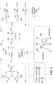
- the system 100 may include an aggregation circuit 110, an SDM 120, a transmitter 132, a receiver 134 and a separation circuit 140.
- the aggregation circuit 110 may: implement a multiplier 111 to form a bandpass signal s1 by multiplication of a source signal D1 and a transmitter oscillation signal TO1, implement a multiplier 112 to form a bandpass signal s2 by multiplication of a source signal D2 and a transmitter oscillation signal TO2, implement a sum block 113 to form a summed bandpass signal ss1 by summing the signals s1 and s2, and implement another sum block 114 to form an aggregated signal sa1 by summing the signals ss1 and another source signal D3.
- the signals D1, D2 and D3 may be discrete-time digital baseband signals at a low-pass band LB, and each of the signals D1, D2 and D3 may contain desired data and/or information.
- Each of the signals TO1 and TO2 may be a discrete-time digital signal sampled at a sampling frequency fs.
- the signals TO1 and TO2 may be sinusoidal signals of the same frequency fP, but a phase of the signal TO1 may differ from a phase of the signal TO2, e.g., by 90 degrees.
- each sample TO1[n] of the signal TO1 may be cos(2*pi*n/M)
- each sample TO2[n] of the signal TO2 may be sin(2*pi*n/M), with M being a ratio dividing the sampling frequency fs by the frequency fP.
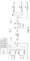
- the aggregation circuit 110 in FIG. 2 may be achieved by an aggregation circuit 110a shown in FIG. 3 ; as shown in FIG. 3 , the aggregation circuit 110a may include two complement converters 311 and 312, a switch (e.g., a multiplexer) 313 and a sum block 314.
- a switch e.g., a multiplexer
- the complement converter 311 may be coupled to the signal D1, for forming a complement of a sample D1[n] of the signal D1, and the complement converter 312 may be coupled to the signal D2, for forming a complement of a sample D2[n] of the signal D2.
- the aggregation circuit 110a may form every four samples ss1[4*k], ss1[4*k+1], ss1[4*k+2] and ss1[4*k+3] of the signal ss1 by: arranging the sample ss1[4*k] of the signal ss1 to equal the sample D1[4*k] of the signal D1, arranging the sample ss1[4*k+1] of the signal ss1 to equal the sample D2[4*k+1] of the signal D2, arranging the sample ss1[4*k+2] of the signal ss1 to equal a complement of the sample D1[4*k+2] of the signal D1, and arranging the sample ss1[4*k+3] of the signal ss1 to equal a complement of the sample D2[4*k+3] of the signal D2.
- the aggregation circuit 110 may form every eight samples ss1[8*k] to ss1[8*k+7] of the signal ss1 by: arranging the sample ss1[8*k] to equal the sample D1[8*k] of the signal D1, arranging the sample ss1[8*k+1] to equal c0*(D1[8*k+1]+D2[8*k+1]), arranging the sample ss1[8*k+2] to equal the sample D2[8*k+2] of the signal D2, arranging the sample ss1[8*k+3] to equal c0*(-D1[8*k+3]+D2[8*k+3]), arranging the sample ss1[8*k+4] to equal a complement of the sample D1[8*k+
- the SDM 120 may be coupled between the aggregated circuit 110 and the transmitter 132, and may modulate the signal sa1 to a modulated signal sb1 with noise shaping.
- modulation of the SDM 120 may reduce bit number per sample and/or throughput, e.g., the SDM 120 may modulate the signal sa1 of more bits per sample and/or higher throughput to the signal sb1 of fewer bits per sample and/or lower throughput.
- the SDM 120 may include a main circuit 121, a noise shaping circuit 122 and a sum block 123.
- the main circuit 121 may transfer the signal sa1 by a signal transfer function STF(z) (with respect to z-transform).
- the noise shaping circuit 122 may be coupled to the sum block 123, for shaping noise away from the low-pass band LB by a modified noise transfer function mNTF(z).
- the sum block 123 may be coupled to the main circuit 121 and the noise shaping circuit 122, and may provide the signal sb1 by summing transferred results of the main circuit 121 and the noise shaping circuit 122.
- a frequency response 126 of the modified noise transfer function mNTF(z) may have a notch 124 at the passband PB. Because of the notch 124 at the passband PB, the SDM 120 will not shape noise into the passband PB, and may then improve spectrum efficiency by enabling the passband PB to be utilized by the desired bandpass signals s1 and s2.
- the frequency response 126 of the modified noise transfer function mNTF(z) may further have a second notch 125 at a high-pass band HB, and the high-pass band HB may not overlap with the passband PB and the low-pass band LB; a frequency fH of the band HB may be higher than the frequency fP of the passband PB, and the frequency fP may be higher than a frequency fL of the band LB.
- the frequency fH of the high-pass band HB may substantially equals a half of the sampling frequency fs. Because of the notch 125, the SDM 120 will not shape noise into the band HB.
- the cleared band HB may be utilized to facilitate detection and/or correction of fault/error.
- the main circuit 121, the noise shaping circuit 122 and the sum block 123 may be formed by an internal circuit 220 shown in FIG. 4 .
- the internal circuit 220 may include a front circuit 222, a feedback circuit 229, a quantizer 226 and sum blocks 228 and 224.
- the front circuit 222 may be coupled to the signals sa1 and sb1, for transferring the signal sa1 and the signal sb1 respectively by a first transfer function L1(z) and a second transfer function -L2(z), so as to form a first signal x1.
- the feedback circuit 229 may be coupled to the main circuit 222 via the sum block 224, for transferring a third signal x3 by a third transfer function L3(z) to form a fourth signal x4.
- the quantizer 226 may be coupled to the front circuit 222 and the feedback circuit 229, for quantizing a second signal x2 to form the signal sb1.
- the signal x1 may be a sum of the signal x1 and the signal x4
- the signal x3 may be a difference between the signal sb1 and the signal x2.
- the SDM 120 in FIG. 2 may be a multi-bit SDM which may modulate the sa1 signal to the signal sb1 of multiple bits per sample; i.e., the quantizer 226 in FIG. 4 may be a multi-bit quantizer.
- a frequency response 226 of the intrinsic noise transfer function iNTF(z) may be configured to shape noise away from the band LB to other bands, including the bands PB and HB.
- the frequency response 226 of the intrinsic noise transfer function mNTF(z) may be configured to have the notch 124 at the passband PB, and have the notch 125 at the band HB, so noise will not be shaped to the bands PB and HB.
- the notches 124 and 125 may be formed by a modifying function (1+L3(z)) equal to a sum of one and the transfer function L3(z), since the modified transfer function mNTF(z) may be a product of the intrinsic noise transfer function iNTF(z) and the modifying function (1+L3(z)).
- the modulated signal sb1 from the SDM 120 may be an interconnection signal of wired interconnection; the transmitter 132 may be coupled to a cascade of the aggregation circuit 110 and the SDM 120, and may transmit the signal sb1 to the receiver 134 via a wired channel 10 (e.g., SerDes channel) between two semiconductor chips (dice). That is, the system 100 may include two portions P1 and P2 respectively formed on two semiconductor chips; the portion P1 may include the aggregation circuit 110, the SDM 120 and the transmitter 132, and the portion P2 may include the receiver 134 and the separation circuit 140.
- a wired channel 10 e.g., SerDes channel
- the receiver 134 may be coupled to the transmitter 132 via the wired channel 10, for receiving the signal sb1 from the transmitter 134 to form a signal sc1.
- the transmitter 132 may be a digital physical layer circuit, for packaging samples of the signal sb1 to packets, and transmitting the packets to the receiver 134; the receiver 134 may be another digital physical layer circuit, for receiving the packets sent by the transmitter 132, and unpacking samples from the packets to form samples of the signal sc1.
- the separation circuit 140 may be coupled to the receiver 134, and may include multipliers 141 and 142, along with filters 143, 144 and 145.
- the multiplier 141 may be coupled to the signal sc1 and a receiver oscillation signal RO1, for implementing multiplication of the signals sc1 and RO1 to form a first separated signal sd1.
- the multiplier 142 may be coupled to the signal sc2 and another receiver oscillation signal RO2, for implementing multiplication of the signals sc1 and RO2 to form a second separated signal sd2.
- the signals RO1 and RO2 may be periodic at the same frequency fP, but have different phases.
- the filter 143 may be coupled to the multiplier 141 for filtering the signals sd1 to form a low-pass baseband signal Dr1, so the signal D1 of the portion P1 may be received as the signal Dr1 at the portion P2.
- the filter 144 may be coupled to the multiplier 142, for filtering the signals sd2 to form a low-pass baseband signal Dr2, so the signal D2 of the portion P1 may be received as the signal D21 at the portion P2.
- the filter 145 may be coupled to the receiver 134, for filtering the signals sd1 to form a low-pass baseband signal Dr3, so the signal D3 of the portion P1 may be received as the signal Dr3 at the portion P2.
- the filters 143, 144 and 145 may be CIC (cascaded integrator-comb) filters.
- the aggregation circuit 110 in FIG. 2 may be simplified to the aggregation circuit 110a in FIG. 3 ; similarly, the separation circuit 140 in FIG. 2 may be simplified to a separation circuit 140a in FIG. 3 .
- the switch 146 may arrange every two consecutive samples sc1[2*n] and sc1[2*n+1] of the received signal sc1 to respectively be the samples sd1[n] of the signal sd1 and the sample sd2[n] of the signal sd2.
- the modified noise transfer function mNTF(z) of the SDM 120 may keep signal sb1 cleared from noise at the band HB, so as to facilitate detection/correction of fault/error.
- the signal sb1 is transmitted from the portions P1 to P2 to form the signal sc1
- the fault/error will contribute nonzero component to the band HB, so the signal sc1 will not be emptied at the band HB.
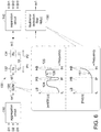
- whether the signal sc1 is emptied at the band HB may be utilized to indicate whether fault/error occurs. For example, in an embodiment shown in FIG.
- the system 100 may further include a fault/error detection filter 150 coupled to the receiver 134 in parallel with the separation circuit 140, for filtering the signal sc1 to form a detection signal sx1 by a transfer function Hd(z), and a frequency response 151 of the transfer function Hd(z) may have a peak at the band HB. If fault/error occurs during the transmission and therefore contributes nonzero component to the band HB, the nonzero component at the band HB will be enhanced by the transfer function Hd(z), and the signal sd1 will saturate to bound(s) of a predefined signal range. By checking if the signal sd1 saturates, the system 100 may detect whether fault/error occurs.
- a fault/error detection filter 150 coupled to the receiver 134 in parallel with the separation circuit 140, for filtering the signal sc1 to form a detection signal sx1 by a transfer function Hd(z), and a frequency response 151 of the transfer function Hd(z) may have a peak at
- the system of the invention may aggregate multiple baseband data streams (e.g., the signals D1 to D3) into a single signal stream (e.g., the signal sa1) for wired interconnection, and the SDM in the system of the invention may avoid shaping noise to the passband, so as to support the aggregation.
- the system of the invention may therefore improve spectrum efficiency of wired interconnection.
Landscapes
- Engineering & Computer Science (AREA)
- Theoretical Computer Science (AREA)
- Signal Processing (AREA)
- Computer Networks & Wireless Communication (AREA)
- Physics & Mathematics (AREA)
- Spectroscopy & Molecular Physics (AREA)
- Compression, Expansion, Code Conversion, And Decoders (AREA)
- Transmission Systems Not Characterized By The Medium Used For Transmission (AREA)
- Amplifiers (AREA)
Abstract
Description
- The present invention relates to sigma-delta modulator (SDM) and associated system improving spectrum efficiency of wired interconnection, and more particularly, to SDM and associated system improving spectrum efficiency by shaping noise with a modified noise transfer function having a frequency-domain notch at a passband, which is therefore available for carrying additional bandpass signal(s) besides low-pass baseband signal(s).
- SDM is broadly exploited in modern electronic systems, such as systems involving discrete-time digital signals sampled at a sampling frequency. Please refer to
FIG. 1 illustrating a conventional spectrum arrangement for baseband signal(s) at a low-pass band. Because of many practical engineering considerations (e.g., matching an integer multiplication of a reference frequency), a sampling frequency fs of the signal(s) is usually set much higher than a Nyquist sampling frequency f_N of the signal(s). The spectrum therefore has a large vacancy, which extends from the low-pass band to an half of the sampling frequency (fs/2), not fully utilized. - An objective of the invention is providing an SDM (e.g., 120 in
FIG. 2 ) improving spectrum efficiency of wired interconnection. The SDM may comprise a main circuit (e.g., 121) and a noise shaping circuit (e.g., 122). The main circuit may be coupled to an aggregated signal (e.g., sa1), for transferring the aggregated signal by a signal transfer function (e.g., STF(z)). The noise shaping circuit may be coupled to the main circuit, for shaping noise away from a low-pass band (e.g., LB) by a modified noise transfer function (e.g., mNTF(z)), wherein a frequency response (e.g., 126) of the modified noise transfer function has a notch (e.g., 124) at a passband (e.g., PB), and the passband may not overlap with the low-pass band. - In an embodiment, the SDM may modulate the aggregated signal to a modulated signal (e.g., sb1 in
FIG. 2 ), and a ratio (e.g., M) dividing a sampling frequency (e.g., fs) of the modulated signal by a frequency (e.g., fP) of the passband may substantially equal a multiplication of four. In an embodiment, the frequency of the passband may substantially equal a quarter of the sampling frequency of the modulated signal. - In an embodiment, the SDM may be a multi-bit SDM modulating the aggregated signal to a modulated signal of multiple bits per sample.
- In an embodiment, the frequency response of the modified noise transfer function may further have a second notch (e.g., 125) at a high-pass band (e.g., HB), and the high-pass band may not overlap with the passband and the low-pass band. In an embodiment, a frequency (e.g., fH) of the high-pass band may substantially equal a half of the sampling frequency of the modulated signal.
- In an embodiment (e.g.,
FIG. 4 ), the main circuit and the noise shaping circuit may be formed by an internal circuit (e.g., 220 inFIG. 4 ), which may comprise a front circuit (e.g., 222), a feedback circuit (e.g., 229) and a quantizer (e.g., 226). The front circuit may be coupled to the aggregated signal, for transferring the aggregated signal and the modulated signal (e.g., sb1) respectively by a first transfer function (e.g., L1(z)) and a second transfer function (e.g., L2(z)), so as to form a first signal (e.g., x1). The feedback circuit may be coupled to the front circuit, for transferring a third signal (e.g., x3) by a third transfer function (e.g., L3(z)) to form a fourth signal (e.g., x4). The quantizer may be coupled to the front circuit and the feedback circuit, for quantizing a second signal (e.g., x2) to form the modulated signal, wherein the second signal may be a sum of the first signal and the fourth signal, the third signal may be a difference between the modulated signal and the second signal, and the notch may be formed by a modifying function (e.g., 1+L3(z)) equal to a sum of one and the third transfer function. In an embodiment, the modifying function (e.g., 1+L3(z)) may have one or more zeros at a square root of negative one. - In an embodiment, the aggregated signal may contain one or more desired signals (e.g., s1, s2) at the passband.
- In an embodiment, the SDM may be included in a system (e.g., 100 in
FIG. 2 ), and the system may further include an aggregation circuit (e.g., 110) and a transmitter (e.g., 132). - An objective of the invention is providing a system (e.g., 100 in
FIG. 2 ) improving spectrum efficiency of wired interconnection. The system may include an aggregation circuit (e.g., 110) and a transmitter (e.g., 132). The aggregation circuit may sum one or more bandpass signals (e.g., s1 and/or s2) and a low-pass signal (e.g., D3). The transmitter may be coupled to the aggregation circuit, for transmitting, via a wired channel (e.g., 10), an interconnection signal (e.g., sb1) resulting from the aggregation circuit (and the SDM). The said one or more bandpass signals may be at a passband (e.g., PB), the low-pass signal may be at a low-pass band (e.g., LB); and, the passband may not overlap with the low-pass band. - In an embodiment, a frequency (e.g., fP) of the passband may substantially equal a quarter of a sampling frequency (e.g., fs) of the interconnection signal.
- In an embodiment, the aggregation circuit may further implement multiplication of a first source signal (e.g., D1) and a first transmitter oscillation signal (e.g., TO1) to form a first one (e.g., s1) of said one or more bandpass signals, and may further implement multiplication of a second source signal (e.g., D2) and a second transmitter oscillation signal (e.g., TO2) to form a second one (e.g., s2) of said one or more bandpass signals, wherein a phase of the second transmitter oscillation signal may differ from a phase of the first transmitter oscillation signal.
- In an embodiment, the system may further comprise a receiver (e.g., 134) and a separation circuit (e.g., 140). The receiver may be coupled to the transmitter, for receiving the interconnection signal from the transmitter to form a received signal (e.g., sc1). The separation circuit may be coupled to the receiver, may implement multiplication of the received signal and a first receiver oscillation signal (e.g., RO1) to form a first separated signal (e.g., sd1), and may further implement multiplication of the received signal and a second receiver oscillation signal (e.g., RO2) to form a second separated signal (e.g., sd2).
- In an embodiment, said one or more bandpass signals may include a first bandpass signal (e.g., s1), and the aggregation circuit may further form every four or more samples (e.g., s1[4*k] to s1[4*k+3]) of the first bandpass signal from every four or more samples (e.g., D1[4*k] to D1[4*k+3]) of a first source signal (e.g., D1) by: arranging a first one (e.g., s1[4*k]) of the four or more samples of the first bandpass signal to equal a first one (e.g., D1[4*k]) of the four or more samples of the first source signal, arranging a second one (e.g., s1[4*k+1]) of the four or more samples of the first bandpass signal to equal zero, arranging a third one (e.g., s1[4*k+2]) of the four or more samples of the first bandpass signal to equal a complement (e.g., -D1[4*k+2]) of a third one of the four or more samples of the first source signal, and arranging a fourth one (e.g., s1[4*k+3]) of the four or more samples of the first bandpass signal to equal zero.
- In an embodiment, said one or more bandpass signals may include a summed bandpass signal (e.g., ss1); and the aggregation circuit may further form every four or more samples (e.g., e.g., ss1[4*k] to ss1[4*k+3]) of the summed bandpass signal from every four or more samples (e.g., D1[4*k] to D1[4*k+3]) of a first source signal (e.g., D1) and every four or more samples (e.g., D2[4*k] to D2[4*k+3]) of a second source signal (e.g., D2) by: arranging a first one (e.g., ss1[4*k]) of the four or more samples of the summed bandpass signal to equal a first one (e.g., D1[4*k]) of the four or more samples of the first source signal, arranging a second one (e.g., ss1[4*k+1]) of the four or more samples of the summed bandpass signal to equal a second one (e.g., D2[4*k+1]) of the four or more samples of the second source signal, arranging a third one (e.g., ss1[4*k+2]) of the four or more samples of the summed bandpass signal to equal a complement (e.g., -D1[4*k+2]) of a third one of the four or more samples of the first source signal, and arranging a fourth one (e.g., ss1[4*k+3]) of the four or more samples of the summed bandpass signal to equal a complement (e.g., -D2[4*k+3]) of a fourth one of the four or more samples of the second source signal.
- In an embodiment (e.g.,
FIG. 3 ), the system may further comprise a receiver (e.g., 134) and a separation circuit (e.g., 140a inFIG. 3 ). The receiver may be coupled to the transmitter, for receiving the interconnection signal from the transmitter to form a received signal (e.g., sc1). The separation circuit may be coupled to the receiver, for separating the received signal to a first separated signal (e.g., sd1) and a second separated signal (e.g., sd2) by: arranging every two consecutive samples of the received signal to respectively be a samples of the first separated signal and a sample of the second separated signal. - In an embodiment, the system may further comprise an SDM (e.g., 120) coupled between the aggregation circuit and the transmitter, for modulating an aggregated signal (e.g., sa1) resulting from the aggregation circuit, with noise shaped away from the low-pass band by a modified noise transfer function (e.g., mNTF(z)), so as to form the interconnection signal; wherein a frequency response (e.g., 126) of the modified noise transfer function may have a notch (e.g., 124) at the passband. In an embodiment, the frequency response of the modified noise transfer function may further have a second notch (e.g., 125 in
FIG. 2 ) at a high-pass band (e.g., HB), and the high-pass band may not overlap with the passband and the low-pass band. - In an embodiment, a frequency (e.g., fH) of the high-pass band may substantially equal a half of the sampling frequency of the interconnection signal.
- Numerous objects, features and advantages of the present invention will be readily apparent upon a reading of the following detailed description of embodiments of the present invention when taken in conjunction with the accompanying drawings. However, the drawings employed herein are for the purpose of descriptions and should not be regarded as limiting.
- The above objects and advantages of the present invention will become more readily apparent to those ordinarily skilled in the art after reviewing the following detailed description and accompanying drawings, in which:
-
FIG. 1 (prior art) illustrates a conventional spectrum arrangement; -
FIG. 2 illustrates a system according to an embodiment of the invention; -
FIG. 3 illustrates a system according to an embodiment of the invention; -
FIG. 4 illustrates an internal circuit of an SDM according to an embodiment of the invention; -
FIG. 5 illustrates frequency responses of different noise transfer functions related to the SDM shown inFIG. 4 ; and -
FIG. 6 illustrates a system according to an embodiment of the invention. - Please refer to
FIG. 2 illustrating asystem 100 according to an embodiment of the invention. Thesystem 100 may include anaggregation circuit 110, anSDM 120, atransmitter 132, areceiver 134 and aseparation circuit 140. Theaggregation circuit 110 may: implement amultiplier 111 to form a bandpass signal s1 by multiplication of a source signal D1 and a transmitter oscillation signal TO1, implement amultiplier 112 to form a bandpass signal s2 by multiplication of a source signal D2 and a transmitter oscillation signal TO2, implement asum block 113 to form a summed bandpass signal ss1 by summing the signals s1 and s2, and implement anothersum block 114 to form an aggregated signal sa1 by summing the signals ss1 and another source signal D3. - The signals D1, D2 and D3 may be discrete-time digital baseband signals at a low-pass band LB, and each of the signals D1, D2 and D3 may contain desired data and/or information. Each of the signals TO1 and TO2 may be a discrete-time digital signal sampled at a sampling frequency fs. Each sample s1[n] of the signal s1 may be a multiplication of a sample D1[n] of the signal D1 and a sample TO1[n] of the signal TO1, i.e., s1[n] = D1[n]*TO1[n]; each sample s2[n] of the signal s2 may be a multiplication of a sample D2[n] of the signal D2 and a sample TO2[n] of the signal TO2, i.e., s2[n] = D2[n]*TO2[n].
- Each of the signals TO1 and TO2 may be periodic at a frequency fP, so the signals s1 = D1*TO1 and s2 = D2*TO2 may be bandpass signals at a passband PB enclosing the frequency fP. As shown in
FIG. 2 , the passband PB may not overlap with the low-pass band LB. By summing the low-pass signal D3 and the bandpass signals s1 and s2, the signal sa1 resulting from theaggregation circuit 110 may contain desired signals not only at the low-pass band LB, but also at the passband PB. - In an embodiment, the signals TO1 and TO2 may be sinusoidal signals of the same frequency fP, but a phase of the signal TO1 may differ from a phase of the signal TO2, e.g., by 90 degrees. For example, in an embodiment, each sample TO1[n] of the signal TO1 may be cos(2*pi*n/M), and each sample TO2[n] of the signal TO2 may be sin(2*pi*n/M), with M being a ratio dividing the sampling frequency fs by the frequency fP. Thus, each sample s1[n] of the signal s1 may be expressed by s1[n] = D1[n]*cos(2*pi*n/M), and each sample s2[n] of the signal s2 may be expressed by s2[n] = D2[n]*sin(2*pi*n/M). In an embodiment, the ratio M = fs/fP may be an integer multiplication of 4, i.e., M = 4*M0 with M0 being a constant integer; for example, the ratio M may be set equal to 4, 8 or 12, etc.; that is, the frequency fP may be set equal to fs/4, fs/8 or fs/12, etc. With the ratio M set to be an integer multiplication of 4, the
aggregation circuit 110 may form the bandpass signal ss1 by circuitry of low complexity. - For example, in an embodiment, the ratio M = fs/fP may equal 4, so every four samples TO1[4*k], TO1[4*k+1], TO1[4*k+2] and TO1[4*k+3] of the signal TO1 will respectively equal 1, 0, -1 and 0, and corresponding four samples s1[4*k], s1[4*k+1], s1[4*k+2] and s1[4*k+3] of the signal s1 will therefore equal D1[4*k], 0, -D1[4*k+2] and 0. That is, with the ratio M set equal to 4, the
aggregation circuit 110 may not actually need a physical multiplying circuit for multiplying the signals D1 and TO1 to form the signal s1; theaggregation circuit 110 may form every four samples s1[4*k], s1[4*k+1], s1[4*k+2] and s1[4*k+3] of the signal s1 simply by: arranging the sample s1[4*k] of the signal s1 to equal the sample D1[4*k] of the signal D1, arranging the sample s1[4*k+1] of the signal s1 to equal zero, arranging the sample s1[4*k+2] of the signal s1 to equal a complement of the sample D1[4*k+2] of the signal D1 (i.e., s1[4*k+2] = -D1[4*k+2]), and arranging the sample s1[4*k+3] of the signal s1 to equal zero. Similarly, with M = 4, every four samples TO2[4*k], TO2[4*k+1], TO2[4*k+2] and TO2[4*k+3] of the signal TO2 will respectively equal 0, 1, 0 and -1, and corresponding four samples s2[4*k], s2[4*k+1], s2[4*k+2] and s2[4*k+3] of the signal s2 will therefore equal 0, D2[4*k+1], 0, -D2[4*k+3]. Accordingly, every four sample ss1[4*k], ss1[4*k+1 ], ss1[4*k+2] and ss1[4*k+3] of the summed signal ss1 = s1+s2 will therefore respectively equal D1[4*k], D2[4*k+1], -D1[4*k+2] and -D2[4*k+2]. - That is, with the ratio M = fs/fP set equal to 4 (i.e., fP = fs/4) by setting the frequency fP substantially equal to a quarter of the sampling frequency fs, the
aggregation circuit 110 inFIG. 2 may be achieved by anaggregation circuit 110a shown inFIG. 3 ; as shown inFIG. 3 , theaggregation circuit 110a may include twocomplement converters sum block 314. Thecomplement converter 311 may be coupled to the signal D1, for forming a complement of a sample D1[n] of the signal D1, and thecomplement converter 312 may be coupled to the signal D2, for forming a complement of a sample D2[n] of the signal D2. Theswitch 313 may be coupled to the signals D1 and D2, as well as thecomplement converters aggregation circuit 110a may form every four samples ss1[4*k], ss1[4*k+1], ss1[4*k+2] and ss1[4*k+3] of the signal ss1 by: arranging the sample ss1[4*k] of the signal ss1 to equal the sample D1[4*k] of the signal D1, arranging the sample ss1[4*k+1] of the signal ss1 to equal the sample D2[4*k+1] of the signal D2, arranging the sample ss1[4*k+2] of the signal ss1 to equal a complement of the sample D1[4*k+2] of the signal D1, and arranging the sample ss1[4*k+3] of the signal ss1 to equal a complement of the sample D2[4*k+3] of the signal D2. Thesum block 314 may sum the signals ss1 and D3 to calculate the signal sa1. It is therefore noted that, with the ratio M set equal to 4, multiplying operations involved in calculating the signal ss1 = D1*TO1+D2*TO2 may be eliminated, and themultipliers sum block 113 in the aggregation circuit 110 (FIG. 2 ) may be simplified to thecomplement converters switch 313 in theaggregation circuit 110a (FIG. 3 ). - In an embodiment with the ratio M = fs/fP set equal to 8 (i.e., fP = fs/8), the aggregation circuit 110 (
FIG. 2 ) may form every eight samples ss1[8*k] to ss1[8*k+7] of the signal ss1 by: arranging the sample ss1[8*k] to equal the sample D1[8*k] of the signal D1, arranging the sample ss1[8*k+1] to equal c0*(D1[8*k+1]+D2[8*k+1]), arranging the sample ss1[8*k+2] to equal the sample D2[8*k+2] of the signal D2, arranging the sample ss1[8*k+3] to equal c0*(-D1[8*k+3]+D2[8*k+3]), arranging the sample ss1[8*k+4] to equal a complement of the sample D1[8*k+4] (i.e., -D1[8*k+4]), arranging the sample ss1[8*k+5] to equal c0*(-D1[8*k+5]-D2[8*k+5]), arranging the sample ss1[8*k+6] to equal a complement of the sample D2[8*k+6] (i.e., -D2[8*k+6]), and arranging the sample ss1[8*k+7] to equal c0*(D1[8*k+7]-D2[8*k+7]), wherein the term c0 is a constant equal to a half of a square root of 2. It is therefore noted that, with the ratio M set to 8, multiplying operations involved in calculating the signal ss1 = D1*TO1+D2*TO2 may be simplified to a multiplication of the constant c0, and thus circuitry complexity of theaggregation circuit 110 may be reduced. - In the
system 100 shown inFIG. 2 , theSDM 120 may be coupled between the aggregatedcircuit 110 and thetransmitter 132, and may modulate the signal sa1 to a modulated signal sb1 with noise shaping. In an embodiment, modulation of theSDM 120 may reduce bit number per sample and/or throughput, e.g., theSDM 120 may modulate the signal sa1 of more bits per sample and/or higher throughput to the signal sb1 of fewer bits per sample and/or lower throughput. - As shown in
FIG. 2 , theSDM 120 may include amain circuit 121, anoise shaping circuit 122 and asum block 123. Themain circuit 121 may transfer the signal sa1 by a signal transfer function STF(z) (with respect to z-transform). Thenoise shaping circuit 122 may be coupled to thesum block 123, for shaping noise away from the low-pass band LB by a modified noise transfer function mNTF(z). Thesum block 123 may be coupled to themain circuit 121 and thenoise shaping circuit 122, and may provide the signal sb1 by summing transferred results of themain circuit 121 and thenoise shaping circuit 122. Operation of theSDM 120 may therefore be expressed as Sb1(z) = STF(z)*Sa1(z)+mNTF(z)*Q(z), with Sa1(z) and Sb1(z) denoting z-transform of the signals sa1 and sb1, and Q(z) denoting noise. As shown inFIG. 2 , afrequency response 126 of the modified noise transfer function mNTF(z) may have anotch 124 at the passband PB. Because of thenotch 124 at the passband PB, theSDM 120 will not shape noise into the passband PB, and may then improve spectrum efficiency by enabling the passband PB to be utilized by the desired bandpass signals s1 and s2. - In an embodiment, as shown in
FIG. 2 , thefrequency response 126 of the modified noise transfer function mNTF(z) may further have asecond notch 125 at a high-pass band HB, and the high-pass band HB may not overlap with the passband PB and the low-pass band LB; a frequency fH of the band HB may be higher than the frequency fP of the passband PB, and the frequency fP may be higher than a frequency fL of the band LB. In an embodiment, the frequency fH of the high-pass band HB may substantially equals a half of the sampling frequency fs. Because of thenotch 125, theSDM 120 will not shape noise into the band HB. The cleared band HB may be utilized to facilitate detection and/or correction of fault/error. - In the
SDM 120, themain circuit 121, thenoise shaping circuit 122 and thesum block 123 may be formed by aninternal circuit 220 shown inFIG. 4 . As shown inFIG. 4 , theinternal circuit 220 may include afront circuit 222, afeedback circuit 229, aquantizer 226 and sum blocks 228 and 224. Thefront circuit 222 may be coupled to the signals sa1 and sb1, for transferring the signal sa1 and the signal sb1 respectively by a first transfer function L1(z) and a second transfer function -L2(z), so as to form a first signal x1. Thefeedback circuit 229 may be coupled to themain circuit 222 via thesum block 224, for transferring a third signal x3 by a third transfer function L3(z) to form a fourth signal x4. Thequantizer 226 may be coupled to thefront circuit 222 and thefeedback circuit 229, for quantizing a second signal x2 to form the signal sb1. By the sum blocks 224 and 228, the signal x1 may be a sum of the signal x1 and the signal x4, the signal x3 may be a difference between the signal sb1 and the signal x2. In an embodiment, theSDM 120 inFIG. 2 may be a multi-bit SDM which may modulate the sa1 signal to the signal sb1 of multiple bits per sample; i.e., thequantizer 226 inFIG. 4 may be a multi-bit quantizer. - Operation of the
internal circuit 220 may be expressed as Sb1(z) = L1(z)*Sa1(z)/(1+L2(z)) + (1+L3(z))*Q(z), thus the signal transfer function STF(z) may equal L1(z)/(1+L2(z)), and the modified noise transfer function mNTF(z) may equal (1+L3(z))/(1+L2(z)). With 1/(L2(z)) being an intrinsic noise transfer function iNTF(z), the modified noise transfer function mNTF(z) may be expressed as (1+L3(z))*iNTF(z). As shown inFIG. 5 , afrequency response 226 of the intrinsic noise transfer function iNTF(z) may be configured to shape noise away from the band LB to other bands, including the bands PB and HB. On the other hand, as previously described, thefrequency response 226 of the intrinsic noise transfer function mNTF(z) may be configured to have thenotch 124 at the passband PB, and have thenotch 125 at the band HB, so noise will not be shaped to the bands PB and HB. Thenotches notch 124 at the frequency fP = fs/4. In an embodiment, the modifying function (1+L3(z)) may have one or more zeros at -1, so as to form thenotch 125 at the frequency fH = fs/2. - In the
system 100 shown inFIG. 2 , the modulated signal sb1 from theSDM 120 may be an interconnection signal of wired interconnection; thetransmitter 132 may be coupled to a cascade of theaggregation circuit 110 and theSDM 120, and may transmit the signal sb1 to thereceiver 134 via a wired channel 10 (e.g., SerDes channel) between two semiconductor chips (dice). That is, thesystem 100 may include two portions P1 and P2 respectively formed on two semiconductor chips; the portion P1 may include theaggregation circuit 110, theSDM 120 and thetransmitter 132, and the portion P2 may include thereceiver 134 and theseparation circuit 140. Thereceiver 134 may be coupled to thetransmitter 132 via the wiredchannel 10, for receiving the signal sb1 from thetransmitter 134 to form a signal sc1. In an embodiment, thetransmitter 132 may be a digital physical layer circuit, for packaging samples of the signal sb1 to packets, and transmitting the packets to thereceiver 134; thereceiver 134 may be another digital physical layer circuit, for receiving the packets sent by thetransmitter 132, and unpacking samples from the packets to form samples of the signal sc1. - The
separation circuit 140 may be coupled to thereceiver 134, and may includemultipliers filters multiplier 141 may be coupled to the signal sc1 and a receiver oscillation signal RO1, for implementing multiplication of the signals sc1 and RO1 to form a first separated signal sd1. Themultiplier 142 may be coupled to the signal sc2 and another receiver oscillation signal RO2, for implementing multiplication of the signals sc1 and RO2 to form a second separated signal sd2. In an embodiment, similar to the signals TO1 and TO2, the signals RO1 and RO2 may be periodic at the same frequency fP, but have different phases. Thefilter 143 may be coupled to themultiplier 141 for filtering the signals sd1 to form a low-pass baseband signal Dr1, so the signal D1 of the portion P1 may be received as the signal Dr1 at the portion P2. Thefilter 144 may be coupled to themultiplier 142, for filtering the signals sd2 to form a low-pass baseband signal Dr2, so the signal D2 of the portion P1 may be received as the signal D21 at the portion P2. Thefilter 145 may be coupled to thereceiver 134, for filtering the signals sd1 to form a low-pass baseband signal Dr3, so the signal D3 of the portion P1 may be received as the signal Dr3 at the portion P2. In an embodiment, thefilters - As previously described, by setting the frequency fP substantially equal to a quarter of the sampling frequency fs, the ratio M = fs/fP may equal 4, and the
aggregation circuit 110 inFIG. 2 may be simplified to theaggregation circuit 110a inFIG. 3 ; similarly, theseparation circuit 140 inFIG. 2 may be simplified to aseparation circuit 140a inFIG. 3 . As shown inFIG. 3 , themultipliers FIG. 2 may be simplified to aswitch 146 coupled between thereceiver 134 and thefilters switch 146 may arrange every two consecutive samples sc1[2*n] and sc1[2*n+1] of the received signal sc1 to respectively be the samples sd1[n] of the signal sd1 and the sample sd2[n] of the signal sd2. - As previously described, the modified noise transfer function mNTF(z) of the
SDM 120 may keep signal sb1 cleared from noise at the band HB, so as to facilitate detection/correction of fault/error. When the signal sb1 is transmitted from the portions P1 to P2 to form the signal sc1, if fault/error occurs during the transmission, the fault/error will contribute nonzero component to the band HB, so the signal sc1 will not be emptied at the band HB. Thus, whether the signal sc1 is emptied at the band HB may be utilized to indicate whether fault/error occurs. For example, in an embodiment shown inFIG. 6 , thesystem 100 may further include a fault/error detection filter 150 coupled to thereceiver 134 in parallel with theseparation circuit 140, for filtering the signal sc1 to form a detection signal sx1 by a transfer function Hd(z), and afrequency response 151 of the transfer function Hd(z) may have a peak at the band HB. If fault/error occurs during the transmission and therefore contributes nonzero component to the band HB, the nonzero component at the band HB will be enhanced by the transfer function Hd(z), and the signal sd1 will saturate to bound(s) of a predefined signal range. By checking if the signal sd1 saturates, thesystem 100 may detect whether fault/error occurs. In an embodiment, the transfer function Hd(z) may have one or more poles at -1 to form the peak at the frequency fH = fs/2; for example, in an embodiment, the transfer function Hd(z) may equal c1/(1+z^(-1)), with c1 being a constant. - To sum up, by fully utilizing passband which is vacant due to oversampling, the system of the invention may aggregate multiple baseband data streams (e.g., the signals D1 to D3) into a single signal stream (e.g., the signal sa1) for wired interconnection, and the SDM in the system of the invention may avoid shaping noise to the passband, so as to support the aggregation. The system of the invention may therefore improve spectrum efficiency of wired interconnection.
- While the invention has been described in terms of what is presently considered to be the most practical and preferred embodiments, it is to be understood that the invention needs not be limited to the disclosed embodiment. On the contrary, it is intended to cover various modifications and similar arrangements included within the spirit and scope of the appended claims which are to be accorded with the broadest interpretation so as to encompass all such modifications and similar structures.
Claims (15)
- A sigma-delta modulator (SDM, 120) improving spectrum efficiency of wired interconnection, comprising:a main circuit (121) for transferring an aggregated signal (sa1) by a signal transfer function (STF(z)); anda noise shaping circuit (122) coupled to the main circuit, for shaping noise away from a low-pass band (LB) by a modified noise transfer function (mNTF(z));wherein a frequency response (126) of the modified noise transfer function has a notch (124) at a passband (PB), and the passband does not overlap with the low-pass band.
- The SDM of claim 1, wherein the SDM modulates the aggregated signal to a modulated signal (sb1), and a ratio (M) dividing a sampling frequency (fs) of the modulated signal by a frequency (fP) of the passband substantially equals a multiplication of four.
- The SDM of claim 1, wherein the SDM modulates the aggregated signal to a modulated signal (sb1), and a frequency (fP) of the passband substantially equals a quarter of a sampling frequency of the modulated signal.
- The SDM of claim 1 being a multi-bit SDM modulating the aggregated signal to a modulated signal (sb1) of multiple bits per sample.
- The SDM of claim 1, wherein the frequency response of the modified noise transfer function further has a second notch (125) at a high-pass band (HB), and the high-pass band does not overlap with the passband and the low-pass band.
- The SDM of claim 5, wherein the SDM modulates the aggregated signal to a modulated signal (sb1), and a frequency (fH) of the high-pass band substantially equals a half of a sampling frequency of the modulated signal.
- The SDM of claim 1, wherein the main circuit and the noise shaping circuit are formed by an internal circuit (220) which comprises:a front circuit (222) for transferring the aggregated signal and a modulated signal (sb1) respectively by a first transfer function (L1(z)) and a second transfer function (L2(z)), so as to form a first signal (x1);a feedback circuit (229) coupled to the front circuit, for transferring a third signal (x3) by a third transfer function (L3(z)) to form a fourth signal (x4); anda quantizer (226) coupled to the front circuit and the feedback circuit, for quantizing a second signal (x2) to form the modulated signal;wherein the second signal is a sum of the first signal and the fourth signal, the third signal is a difference between the modulated signal and the second signal, andthe notch is formed by a modifying function (1+L3(z)) equal to a sum of one and the third transfer function.
- The SDM of claim 7, wherein the modifying function has one or more zeros at a square root of negative one.
- The SDM of claim 1, wherein the aggregated signal contains one or more desired signals (s1, s2) at the passband.
- The SDM of claim 1 being included in a system (100), and the system further comprising:an aggregation circuit (110, 110a) summing one or more bandpass signals (s1, s2, ss1) and a low-pass signal (D3); anda transmitter (132) coupled to the aggregation circuit, for transmitting, via a wired channel (10), an interconnection signal (sb1) resulting from the SDM;wherein said one or more bandpass signals are at the passband, and the low-pass signal is at the low-pass band.
- The SDM of claim 10, wherein:the aggregation circuit further implements multiplication of a first source signal (D1) and a first transmitter oscillation signal (TO1) to form a first one (s1) of said one or more bandpass signals, and further implements multiplication of a second source signal (D2) and a second transmitter oscillation signal (TO2) to form a second one (s2) of said one or more bandpass signals; anda phase of the second transmitter oscillation signal differs from a phase of the first transmitter oscillation signal.
- The SDM of claim 10, wherein the system further comprises:a receiver (134) coupled to the transmitter, for receiving the interconnection signal from the transmitter to form a received signal (sc1); anda separation circuit (140) coupled to the receiver, implementing multiplication of the received signal and a first receiver oscillation signal (RO1) to form a first separated signal (sd1), and further implementing multiplication of the received signal and a second receiver oscillation signal (RO2) to form a second separated signal (sd2).
- The SDM of claim 10, wherein:said one or more bandpass signals includes a first bandpass signal (s1); andthe aggregation circuit further forms every four or more samples of the first bandpass signal from every four or more samples of a first source signal (D1) by:arranging a first one of the four or more samples of the first bandpass signal to equal a first one of the four or more samples of the first source signal;arranging a second one of the four or more samples of the first bandpass signal to equal zero;arranging a third one of the four or more samples of the first bandpass signal to equal a complement of a third one of the four or more samples of the first source signal; andarranging a fourth one of the four or more samples of the first bandpass signal to equal zero.
- The SDM of claim 10, wherein:said one or more bandpass signals includes a summed bandpass signal (ss1); andthe aggregation circuit (110a) further forms every four or more samples of the summed bandpass signal from every four or more samples of a first source signal (D1) and every four or more samples of a second source signal (D2) by:arranging a first one (ss1[4*k]) of the four or more samples of the summed bandpass signal to equal a first one (D1[4*k]) of the four or more samples of the first source signal;arranging a second one (ss1[4*k+1]) of the four or more samples of the summed bandpass signal to equal a second one (D2[4*k+1]) of the four or more samples of the second source signal;arranging a third one (ss1[4*k+2]) of the four or more samples of the summed bandpass signal to equal a complement (-D1[4*k+2]) of a third one of the four or more samples of the first source signal; andarranging a fourth one (ss1[4*k+3]) of the four or more samples of the summed bandpass signal to equal a complement (-D2[4*k+3]) of a fourth one of the four or more samples of the second source signal
- The SDM of claim 10, wherein the system further comprises:a receiver (134) coupled to the transmitter, for receiving the interconnection signal from the transmitter to form a received signal (sc1); anda separation circuit (140a) coupled to the receiver, for separating the received signal to a first separated signal (sd1) and a second separated signal (sd2) by:
arranging every two consecutive samples of the received signal to respectively be a samples of the first separated signal and a sample of the second separated signal.
Applications Claiming Priority (2)
| Application Number | Priority Date | Filing Date | Title |
|---|---|---|---|
| US201762550040P | 2017-08-25 | 2017-08-25 | |
| US16/044,749 US10341148B2 (en) | 2017-08-25 | 2018-07-25 | Sigma-delta modulator and associated system improving spectrum efficiency of wired interconnection |
Publications (2)
| Publication Number | Publication Date |
|---|---|
| EP3447923A1 true EP3447923A1 (en) | 2019-02-27 |
| EP3447923B1 EP3447923B1 (en) | 2022-03-23 |
Family
ID=63143047
Family Applications (1)
| Application Number | Title | Priority Date | Filing Date |
|---|---|---|---|
| EP18187020.5A Active EP3447923B1 (en) | 2017-08-25 | 2018-08-02 | Sigma-delta modulator and associated system improving spectrum efficiency of wired interconnection |
Country Status (4)
| Country | Link |
|---|---|
| US (1) | US10341148B2 (en) |
| EP (1) | EP3447923B1 (en) |
| CN (1) | CN109428600B (en) |
| TW (1) | TWI692215B (en) |
Cited By (1)
| Publication number | Priority date | Publication date | Assignee | Title |
|---|---|---|---|---|
| EP3709500B1 (en) * | 2019-03-12 | 2024-11-06 | Schneider Toshiba Inverter Europe SAS | Estimation of the amplitude of a periodic component in a measured signal through a delta-sigma modulator |
Citations (1)
| Publication number | Priority date | Publication date | Assignee | Title |
|---|---|---|---|---|
| US20110175762A1 (en) * | 2010-01-15 | 2011-07-21 | Asahi Kasei Microdevices Corporation | Second order noise coupling with zero optimization modulator and method |
Family Cites Families (18)
| Publication number | Priority date | Publication date | Assignee | Title |
|---|---|---|---|---|
| US6642874B1 (en) * | 2002-10-11 | 2003-11-04 | Realtek Semiconductor Corp. | Sigma-delta data conversion employing quantization error feedback |
| US6842486B2 (en) * | 2003-01-21 | 2005-01-11 | Cirrus Logic, Inc. | Signal processing system with baseband noise modulation and noise fold back reduction |
| US7136430B2 (en) * | 2003-03-31 | 2006-11-14 | Nortel Networks Limited | Digital receiver and method |
| US7928876B2 (en) * | 2004-04-09 | 2011-04-19 | Audioasics A/S | Sigma delta modulator |
| FI20065832A0 (en) * | 2006-12-21 | 2006-12-21 | Nokia Corp | An apparatus comprising a frequency selective circuit and a method |
| WO2010046859A1 (en) * | 2008-10-23 | 2010-04-29 | Nxp B.V. | Sigma-delta modulator |
| US8570200B2 (en) * | 2011-01-20 | 2013-10-29 | Mediatek Singapore Pte. Ltd. | Continuous-time oversampled converter having enhanced immunity to noise |
| JP5919712B2 (en) * | 2011-10-04 | 2016-05-18 | 住友電気工業株式会社 | Transmitter, communication system, and radio base station apparatus |
| WO2013051641A1 (en) * | 2011-10-04 | 2013-04-11 | 住友電気工業株式会社 | Design method for bandpass δς modulator, bandpass δς modulator, device having bandpass δς modulator, and method using bandpass δς modulation |
| KR101214976B1 (en) * | 2011-11-01 | 2012-12-24 | 포항공과대학교 산학협력단 | Noise shaping time digital converter using a delta sigma modulating method |
| CN103326728B (en) * | 2013-07-09 | 2016-03-16 | 东南大学 | A kind of noise suppressed strengthens sigma Delta modulator structure |
| US20150085902A1 (en) * | 2013-09-23 | 2015-03-26 | Qualcomm Incorporated | RFDAC Transmitter Using Multiphase Image Select FIR DAC and Delta Sigma Modulator with Multiple Rx Band NTF Zeros |
| US9166617B1 (en) * | 2014-03-31 | 2015-10-20 | Freescale Semiconductor, Inc. | Communication unit, digital band-pass sigma-delta modulator and method therefor |
| CN107111772B (en) * | 2014-09-22 | 2020-12-25 | Drnc控股公司 | Transmission apparatus for wireless device using delta-sigma modulation |
| US9294079B1 (en) * | 2014-11-10 | 2016-03-22 | Mitsubishi Electric Research Laboratories, Inc. | System and method for generating multi-band signal |
| US9300305B1 (en) * | 2014-12-02 | 2016-03-29 | Mediatek Inc. | Frequency synthesizer and related method for improving power efficiency |
| KR102384362B1 (en) * | 2015-07-17 | 2022-04-07 | 삼성전자주식회사 | Delta sigma modulator for shaping noise and audio codec having the same |
| KR102096294B1 (en) * | 2017-06-15 | 2020-04-03 | 선전 구딕스 테크놀로지 컴퍼니, 리미티드 | Noise shaping circuit and sigma-delta digital-to-analog converter |
-
2018
- 2018-07-25 US US16/044,749 patent/US10341148B2/en active Active
- 2018-08-02 EP EP18187020.5A patent/EP3447923B1/en active Active
- 2018-08-10 CN CN201810911685.3A patent/CN109428600B/en active Active
- 2018-08-13 TW TW107128145A patent/TWI692215B/en active
Patent Citations (1)
| Publication number | Priority date | Publication date | Assignee | Title |
|---|---|---|---|---|
| US20110175762A1 (en) * | 2010-01-15 | 2011-07-21 | Asahi Kasei Microdevices Corporation | Second order noise coupling with zero optimization modulator and method |
Non-Patent Citations (1)
| Title |
|---|
| JIQIN HE ET AL: "Dual-band transmitters based on Lowpass and Bandpass delta-sigma modulators", 2016 IEEE INTERNATIONAL CONFERENCE ON MICROWAVE AND MILLIMETER WAVE TECHNOLOGY (ICMMT), IEEE, vol. 2, 5 June 2016 (2016-06-05), pages 590 - 592, XP033013968, DOI: 10.1109/ICMMT.2016.7762377 * |
Cited By (1)
| Publication number | Priority date | Publication date | Assignee | Title |
|---|---|---|---|---|
| EP3709500B1 (en) * | 2019-03-12 | 2024-11-06 | Schneider Toshiba Inverter Europe SAS | Estimation of the amplitude of a periodic component in a measured signal through a delta-sigma modulator |
Also Published As
| Publication number | Publication date |
|---|---|
| CN109428600A (en) | 2019-03-05 |
| US20190068415A1 (en) | 2019-02-28 |
| TWI692215B (en) | 2020-04-21 |
| US10341148B2 (en) | 2019-07-02 |
| CN109428600B (en) | 2022-08-23 |
| EP3447923B1 (en) | 2022-03-23 |
| TW201914243A (en) | 2019-04-01 |
Similar Documents
| Publication | Publication Date | Title |
|---|---|---|
| EP0461721B1 (en) | Transmitter comprising an electronic arrangement for generating a modulated carrier signal | |
| CN103166598B (en) | Digital filter and collocation method, electronic equipment and wireless communication system | |
| US20170288693A1 (en) | Continuous time delta-sigma modulator with a time interleaved quantization function | |
| JPH08181573A (en) | Cascaded integrator | |
| JP2012531835A5 (en) | ||
| US12132497B2 (en) | Multipath D/A converter | |
| WO2012048021A2 (en) | Wavelength division multiplexed optical communication system having variable channel spacings and different modulation formats | |
| US11855659B2 (en) | Isolator | |
| CA2745354C (en) | Demultiplexing apparatus, multiplexing apparatus, communication apparatus, and relay satellite | |
| CN102035503B (en) | Filtering device and filtering method of cascaded integral comb filter | |
| US10341148B2 (en) | Sigma-delta modulator and associated system improving spectrum efficiency of wired interconnection | |
| EP2135356A2 (en) | A power amplifier | |
| US9065472B1 (en) | Multi-function reconfigurable delta sigma DAC | |
| WO2014192574A1 (en) | Transmission circuit | |
| JPH0137057B2 (en) | ||
| US11626858B2 (en) | System improving signal handling | |
| US7953184B2 (en) | Direct sampling type wireless receiver and method using the same | |
| JPWO2018230112A1 (en) | ΔΣ modulator, transmitter, semiconductor integrated circuit, distortion compensation method, system, and computer program | |
| Ralph et al. | Using high pass sigma-delta modulation for Class-S power amplifiers | |
| JP2842867B2 (en) | Receiving apparatus and method | |
| JPH09130438A (en) | Wireless device | |
| WO2016098179A1 (en) | Wireless station apparatus, baseband unit and rf unit | |
| JP4161488B2 (en) | Receiver | |
| WO2013183528A1 (en) | Delta-sigma modulation system and digital signal processing device | |
| JP3588560B2 (en) | Receiver |
Legal Events
| Date | Code | Title | Description |
|---|---|---|---|
| PUAI | Public reference made under article 153(3) epc to a published international application that has entered the european phase |
Free format text: ORIGINAL CODE: 0009012 |
|
| STAA | Information on the status of an ep patent application or granted ep patent |
Free format text: STATUS: REQUEST FOR EXAMINATION WAS MADE |
|
| 17P | Request for examination filed |
Effective date: 20180802 |
|
| AK | Designated contracting states |
Kind code of ref document: A1 Designated state(s): AL AT BE BG CH CY CZ DE DK EE ES FI FR GB GR HR HU IE IS IT LI LT LU LV MC MK MT NL NO PL PT RO RS SE SI SK SM TR |
|
| AX | Request for extension of the european patent |
Extension state: BA ME |
|
| RBV | Designated contracting states (corrected) |
Designated state(s): AL AT BE BG CH CY CZ DE DK EE ES FI FR GB GR HR HU IE IS IT LI LT LU LV MC MK MT NL NO PL PT RO RS SE SI SK SM TR |
|
| STAA | Information on the status of an ep patent application or granted ep patent |
Free format text: STATUS: EXAMINATION IS IN PROGRESS |
|
| 17Q | First examination report despatched |
Effective date: 20210407 |
|
| GRAP | Despatch of communication of intention to grant a patent |
Free format text: ORIGINAL CODE: EPIDOSNIGR1 |
|
| STAA | Information on the status of an ep patent application or granted ep patent |
Free format text: STATUS: GRANT OF PATENT IS INTENDED |
|
| INTG | Intention to grant announced |
Effective date: 20220113 |
|
| GRAS | Grant fee paid |
Free format text: ORIGINAL CODE: EPIDOSNIGR3 |
|
| GRAA | (expected) grant |
Free format text: ORIGINAL CODE: 0009210 |
|
| STAA | Information on the status of an ep patent application or granted ep patent |
Free format text: STATUS: THE PATENT HAS BEEN GRANTED |
|
| AK | Designated contracting states |
Kind code of ref document: B1 Designated state(s): AL AT BE BG CH CY CZ DE DK EE ES FI FR GB GR HR HU IE IS IT LI LT LU LV MC MK MT NL NO PL PT RO RS SE SI SK SM TR |
|
| RAP3 | Party data changed (applicant data changed or rights of an application transferred) |
Owner name: MEDIATEK INC. |
|
| REG | Reference to a national code |
Ref country code: GB Ref legal event code: FG4D |
|
| RIN1 | Information on inventor provided before grant (corrected) |
Inventor name: TSAI, JEN-HUAN |
|
| REG | Reference to a national code |
Ref country code: CH Ref legal event code: EP |
|
| REG | Reference to a national code |
Ref country code: DE Ref legal event code: R096 Ref document number: 602018032546 Country of ref document: DE |
|
| REG | Reference to a national code |
Ref country code: IE Ref legal event code: FG4D |
|
| REG | Reference to a national code |
Ref country code: AT Ref legal event code: REF Ref document number: 1478149 Country of ref document: AT Kind code of ref document: T Effective date: 20220415 |
|
| REG | Reference to a national code |
Ref country code: LT Ref legal event code: MG9D |
|
| REG | Reference to a national code |
Ref country code: NL Ref legal event code: MP Effective date: 20220323 |
|
| PG25 | Lapsed in a contracting state [announced via postgrant information from national office to epo] |
Ref country code: SE Free format text: LAPSE BECAUSE OF FAILURE TO SUBMIT A TRANSLATION OF THE DESCRIPTION OR TO PAY THE FEE WITHIN THE PRESCRIBED TIME-LIMIT Effective date: 20220323 Ref country code: RS Free format text: LAPSE BECAUSE OF FAILURE TO SUBMIT A TRANSLATION OF THE DESCRIPTION OR TO PAY THE FEE WITHIN THE PRESCRIBED TIME-LIMIT Effective date: 20220323 Ref country code: NO Free format text: LAPSE BECAUSE OF FAILURE TO SUBMIT A TRANSLATION OF THE DESCRIPTION OR TO PAY THE FEE WITHIN THE PRESCRIBED TIME-LIMIT Effective date: 20220623 Ref country code: LT Free format text: LAPSE BECAUSE OF FAILURE TO SUBMIT A TRANSLATION OF THE DESCRIPTION OR TO PAY THE FEE WITHIN THE PRESCRIBED TIME-LIMIT Effective date: 20220323 Ref country code: HR Free format text: LAPSE BECAUSE OF FAILURE TO SUBMIT A TRANSLATION OF THE DESCRIPTION OR TO PAY THE FEE WITHIN THE PRESCRIBED TIME-LIMIT Effective date: 20220323 Ref country code: BG Free format text: LAPSE BECAUSE OF FAILURE TO SUBMIT A TRANSLATION OF THE DESCRIPTION OR TO PAY THE FEE WITHIN THE PRESCRIBED TIME-LIMIT Effective date: 20220623 |
|
| REG | Reference to a national code |
Ref country code: AT Ref legal event code: MK05 Ref document number: 1478149 Country of ref document: AT Kind code of ref document: T Effective date: 20220323 |
|
| PG25 | Lapsed in a contracting state [announced via postgrant information from national office to epo] |
Ref country code: LV Free format text: LAPSE BECAUSE OF FAILURE TO SUBMIT A TRANSLATION OF THE DESCRIPTION OR TO PAY THE FEE WITHIN THE PRESCRIBED TIME-LIMIT Effective date: 20220323 Ref country code: GR Free format text: LAPSE BECAUSE OF FAILURE TO SUBMIT A TRANSLATION OF THE DESCRIPTION OR TO PAY THE FEE WITHIN THE PRESCRIBED TIME-LIMIT Effective date: 20220624 Ref country code: FI Free format text: LAPSE BECAUSE OF FAILURE TO SUBMIT A TRANSLATION OF THE DESCRIPTION OR TO PAY THE FEE WITHIN THE PRESCRIBED TIME-LIMIT Effective date: 20220323 |
|
| PG25 | Lapsed in a contracting state [announced via postgrant information from national office to epo] |
Ref country code: NL Free format text: LAPSE BECAUSE OF FAILURE TO SUBMIT A TRANSLATION OF THE DESCRIPTION OR TO PAY THE FEE WITHIN THE PRESCRIBED TIME-LIMIT Effective date: 20220323 |
|
| PG25 | Lapsed in a contracting state [announced via postgrant information from national office to epo] |
Ref country code: SM Free format text: LAPSE BECAUSE OF FAILURE TO SUBMIT A TRANSLATION OF THE DESCRIPTION OR TO PAY THE FEE WITHIN THE PRESCRIBED TIME-LIMIT Effective date: 20220323 Ref country code: SK Free format text: LAPSE BECAUSE OF FAILURE TO SUBMIT A TRANSLATION OF THE DESCRIPTION OR TO PAY THE FEE WITHIN THE PRESCRIBED TIME-LIMIT Effective date: 20220323 Ref country code: RO Free format text: LAPSE BECAUSE OF FAILURE TO SUBMIT A TRANSLATION OF THE DESCRIPTION OR TO PAY THE FEE WITHIN THE PRESCRIBED TIME-LIMIT Effective date: 20220323 Ref country code: PT Free format text: LAPSE BECAUSE OF FAILURE TO SUBMIT A TRANSLATION OF THE DESCRIPTION OR TO PAY THE FEE WITHIN THE PRESCRIBED TIME-LIMIT Effective date: 20220725 Ref country code: ES Free format text: LAPSE BECAUSE OF FAILURE TO SUBMIT A TRANSLATION OF THE DESCRIPTION OR TO PAY THE FEE WITHIN THE PRESCRIBED TIME-LIMIT Effective date: 20220323 Ref country code: EE Free format text: LAPSE BECAUSE OF FAILURE TO SUBMIT A TRANSLATION OF THE DESCRIPTION OR TO PAY THE FEE WITHIN THE PRESCRIBED TIME-LIMIT Effective date: 20220323 Ref country code: CZ Free format text: LAPSE BECAUSE OF FAILURE TO SUBMIT A TRANSLATION OF THE DESCRIPTION OR TO PAY THE FEE WITHIN THE PRESCRIBED TIME-LIMIT Effective date: 20220323 Ref country code: AT Free format text: LAPSE BECAUSE OF FAILURE TO SUBMIT A TRANSLATION OF THE DESCRIPTION OR TO PAY THE FEE WITHIN THE PRESCRIBED TIME-LIMIT Effective date: 20220323 |
|
| PG25 | Lapsed in a contracting state [announced via postgrant information from national office to epo] |
Ref country code: PL Free format text: LAPSE BECAUSE OF FAILURE TO SUBMIT A TRANSLATION OF THE DESCRIPTION OR TO PAY THE FEE WITHIN THE PRESCRIBED TIME-LIMIT Effective date: 20220323 Ref country code: IS Free format text: LAPSE BECAUSE OF FAILURE TO SUBMIT A TRANSLATION OF THE DESCRIPTION OR TO PAY THE FEE WITHIN THE PRESCRIBED TIME-LIMIT Effective date: 20220723 Ref country code: AL Free format text: LAPSE BECAUSE OF FAILURE TO SUBMIT A TRANSLATION OF THE DESCRIPTION OR TO PAY THE FEE WITHIN THE PRESCRIBED TIME-LIMIT Effective date: 20220323 |
|
| REG | Reference to a national code |
Ref country code: DE Ref legal event code: R097 Ref document number: 602018032546 Country of ref document: DE |
|
| PLBE | No opposition filed within time limit |
Free format text: ORIGINAL CODE: 0009261 |
|
| STAA | Information on the status of an ep patent application or granted ep patent |
Free format text: STATUS: NO OPPOSITION FILED WITHIN TIME LIMIT |
|
| PG25 | Lapsed in a contracting state [announced via postgrant information from national office to epo] |
Ref country code: DK Free format text: LAPSE BECAUSE OF FAILURE TO SUBMIT A TRANSLATION OF THE DESCRIPTION OR TO PAY THE FEE WITHIN THE PRESCRIBED TIME-LIMIT Effective date: 20220323 |
|
| 26N | No opposition filed |
Effective date: 20230102 |
|
| PG25 | Lapsed in a contracting state [announced via postgrant information from national office to epo] |
Ref country code: MC Free format text: LAPSE BECAUSE OF FAILURE TO SUBMIT A TRANSLATION OF THE DESCRIPTION OR TO PAY THE FEE WITHIN THE PRESCRIBED TIME-LIMIT Effective date: 20220323 |
|
| REG | Reference to a national code |
Ref country code: CH Ref legal event code: PL |
|
| PG25 | Lapsed in a contracting state [announced via postgrant information from national office to epo] |
Ref country code: LU Free format text: LAPSE BECAUSE OF NON-PAYMENT OF DUE FEES Effective date: 20220802 Ref country code: LI Free format text: LAPSE BECAUSE OF NON-PAYMENT OF DUE FEES Effective date: 20220831 Ref country code: CH Free format text: LAPSE BECAUSE OF NON-PAYMENT OF DUE FEES Effective date: 20220831 |
|
| REG | Reference to a national code |
Ref country code: BE Ref legal event code: MM Effective date: 20220831 |
|
| PG25 | Lapsed in a contracting state [announced via postgrant information from national office to epo] |
Ref country code: SI Free format text: LAPSE BECAUSE OF FAILURE TO SUBMIT A TRANSLATION OF THE DESCRIPTION OR TO PAY THE FEE WITHIN THE PRESCRIBED TIME-LIMIT Effective date: 20220323 |
|
| P01 | Opt-out of the competence of the unified patent court (upc) registered |
Effective date: 20230607 |
|
| PG25 | Lapsed in a contracting state [announced via postgrant information from national office to epo] |
Ref country code: IT Free format text: LAPSE BECAUSE OF FAILURE TO SUBMIT A TRANSLATION OF THE DESCRIPTION OR TO PAY THE FEE WITHIN THE PRESCRIBED TIME-LIMIT Effective date: 20220323 Ref country code: IE Free format text: LAPSE BECAUSE OF NON-PAYMENT OF DUE FEES Effective date: 20220802 |
|
| PG25 | Lapsed in a contracting state [announced via postgrant information from national office to epo] |
Ref country code: BE Free format text: LAPSE BECAUSE OF NON-PAYMENT OF DUE FEES Effective date: 20220831 |
|
| PG25 | Lapsed in a contracting state [announced via postgrant information from national office to epo] |
Ref country code: HU Free format text: LAPSE BECAUSE OF FAILURE TO SUBMIT A TRANSLATION OF THE DESCRIPTION OR TO PAY THE FEE WITHIN THE PRESCRIBED TIME-LIMIT; INVALID AB INITIO Effective date: 20180802 |
|
| PG25 | Lapsed in a contracting state [announced via postgrant information from national office to epo] |
Ref country code: MK Free format text: LAPSE BECAUSE OF FAILURE TO SUBMIT A TRANSLATION OF THE DESCRIPTION OR TO PAY THE FEE WITHIN THE PRESCRIBED TIME-LIMIT Effective date: 20220323 Ref country code: CY Free format text: LAPSE BECAUSE OF FAILURE TO SUBMIT A TRANSLATION OF THE DESCRIPTION OR TO PAY THE FEE WITHIN THE PRESCRIBED TIME-LIMIT Effective date: 20220323 |
|
| PG25 | Lapsed in a contracting state [announced via postgrant information from national office to epo] |
Ref country code: TR Free format text: LAPSE BECAUSE OF FAILURE TO SUBMIT A TRANSLATION OF THE DESCRIPTION OR TO PAY THE FEE WITHIN THE PRESCRIBED TIME-LIMIT Effective date: 20220323 |
|
| PG25 | Lapsed in a contracting state [announced via postgrant information from national office to epo] |
Ref country code: MT Free format text: LAPSE BECAUSE OF FAILURE TO SUBMIT A TRANSLATION OF THE DESCRIPTION OR TO PAY THE FEE WITHIN THE PRESCRIBED TIME-LIMIT Effective date: 20220323 |
|
| PGFP | Annual fee paid to national office [announced via postgrant information from national office to epo] |
Ref country code: GB Payment date: 20250612 Year of fee payment: 8 |
|
| PGFP | Annual fee paid to national office [announced via postgrant information from national office to epo] |
Ref country code: FR Payment date: 20250610 Year of fee payment: 8 |
|
| PGFP | Annual fee paid to national office [announced via postgrant information from national office to epo] |
Ref country code: DE Payment date: 20250611 Year of fee payment: 8 |