EP3447682A1 - Semiconductor device and image recognition system - Google Patents
Semiconductor device and image recognition system Download PDFInfo
- Publication number
- EP3447682A1 EP3447682A1 EP18185295.5A EP18185295A EP3447682A1 EP 3447682 A1 EP3447682 A1 EP 3447682A1 EP 18185295 A EP18185295 A EP 18185295A EP 3447682 A1 EP3447682 A1 EP 3447682A1
- Authority
- EP
- European Patent Office
- Prior art keywords
- circuit
- input
- cumulative addition
- flt
- register
- Prior art date
- Legal status (The legal status is an assumption and is not a legal conclusion. Google has not performed a legal analysis and makes no representation as to the accuracy of the status listed.)
- Granted
Links
Images







Classifications
-
- G—PHYSICS
- G06—COMPUTING OR CALCULATING; COUNTING
- G06T—IMAGE DATA PROCESSING OR GENERATION, IN GENERAL
- G06T1/00—General purpose image data processing
- G06T1/20—Processor architectures; Processor configuration, e.g. pipelining
-
- G—PHYSICS
- G06—COMPUTING OR CALCULATING; COUNTING
- G06F—ELECTRIC DIGITAL DATA PROCESSING
- G06F17/00—Digital computing or data processing equipment or methods, specially adapted for specific functions
- G06F17/10—Complex mathematical operations
- G06F17/15—Correlation function computation including computation of convolution operations
- G06F17/153—Multidimensional correlation or convolution
-
- G—PHYSICS
- G06—COMPUTING OR CALCULATING; COUNTING
- G06N—COMPUTING ARRANGEMENTS BASED ON SPECIFIC COMPUTATIONAL MODELS
- G06N3/00—Computing arrangements based on biological models
- G06N3/02—Neural networks
- G06N3/04—Architecture, e.g. interconnection topology
- G06N3/045—Combinations of networks
-
- G—PHYSICS
- G06—COMPUTING OR CALCULATING; COUNTING
- G06N—COMPUTING ARRANGEMENTS BASED ON SPECIFIC COMPUTATIONAL MODELS
- G06N3/00—Computing arrangements based on biological models
- G06N3/02—Neural networks
- G06N3/04—Architecture, e.g. interconnection topology
- G06N3/0464—Convolutional networks [CNN, ConvNet]
-
- G—PHYSICS
- G06—COMPUTING OR CALCULATING; COUNTING
- G06N—COMPUTING ARRANGEMENTS BASED ON SPECIFIC COMPUTATIONAL MODELS
- G06N3/00—Computing arrangements based on biological models
- G06N3/02—Neural networks
- G06N3/06—Physical realisation, i.e. hardware implementation of neural networks, neurons or parts of neurons
- G06N3/063—Physical realisation, i.e. hardware implementation of neural networks, neurons or parts of neurons using electronic means
-
- G—PHYSICS
- G06—COMPUTING OR CALCULATING; COUNTING
- G06N—COMPUTING ARRANGEMENTS BASED ON SPECIFIC COMPUTATIONAL MODELS
- G06N3/00—Computing arrangements based on biological models
- G06N3/02—Neural networks
- G06N3/08—Learning methods
-
- G—PHYSICS
- G06—COMPUTING OR CALCULATING; COUNTING
- G06T—IMAGE DATA PROCESSING OR GENERATION, IN GENERAL
- G06T7/00—Image analysis
- G06T7/0002—Inspection of images, e.g. flaw detection
-
- G—PHYSICS
- G06—COMPUTING OR CALCULATING; COUNTING
- G06V—IMAGE OR VIDEO RECOGNITION OR UNDERSTANDING
- G06V10/00—Arrangements for image or video recognition or understanding
- G06V10/94—Hardware or software architectures specially adapted for image or video understanding
Definitions
- the present disclosure relates to a semiconductor device and, for example, can be applied to a semiconductor device including an image recognition device.
- CNN Convolutional Neural Network
- the CNN is required to repeat a convolution arithmetic operation of an input image and coefficients the number of times corresponding to the number of channels, so that an operation amount is extremely large. Therefore, it is difficult to implement the CNN on a built-in type SoC (Silicon on Chip) whose resource is limited.
- SoC Silicon on Chip
- a semiconductor device has a function to perform cumulative addition for each channel and performs a convolution arithmetic operation in parallel in a plurality of channels.
- Fig. 1 is a diagram for explaining a concept of the convolution arithmetic operation.
- Figs. 2A to 2C are diagrams for explaining a concept of the convolution arithmetic operation and are diagrams showing a product sum arithmetic operation of pixel values of an image and coefficients of a filter.
- an image when an image is simplified and represented by numbers, the image can be considered as a matrix of height ⁇ width.
- an input image is represented by, for example, 4 ⁇ 4 binary values.
- a 2 ⁇ 2 filter as shown in the right of Fig. 1 is applied to such a matrix and a convolution arithmetic operation is performed.
- the filer is overlapped on a most upper left portion of the image, and values in the same positions are multiplied together.
- the results of the multiplication are summed up and outputted.
- the filter is shifted horizontally by one pixel, and the values in the same positions are multiplied together in the same manner.
- the results of the multiplication are summed up and outputted.
- the values of the filter and the input image are multiplied together and summed up until the filter reaches the lower right.
- An embodiment has a function to perform cumulative addition for each channel and performs a convolution arithmetic operation in parallel in a plurality of channels. It is possible to simultaneously and collectively perform the convolution arithmetic operation on channels, the number of which is the same as the number of blocks where the cumulative addition can be performed for each channel, so that processing time can be reduced.
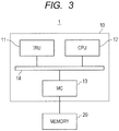
- Fig. 3 is a block diagram showing a configuration example of an image recognition system.
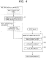
- Fig. 4 is a diagram showing a flow of data of the image recognition system in Fig. 3 .
- an image processing system 1 includes a semiconductor device 10 and a semiconductor storage device (MEMORY) 20.
- the semiconductor device 10 includes an image recognition device (IRU) 11, a central processing unit (CPU) 12, a control circuit (MC) 13 of the semiconductor storage device 20, and a bus that couples these, in a single semiconductor chip.
- the semiconductor storage device 20 is, for example, a DDR-SDRAM.
- an integration coefficient table generation device 50 integrates an input coefficient table included in a pre-integration CNN model stored in a storage device, generates an integration coefficient table of a post-integration CNN model, and stores the integration coefficient table in the semiconductor storage device 20.
- the image recognition device 11 of the image processing system 1 processes an input image stored in the semiconductor storage device 20 on the basis of the integration coefficient table and stores a processing result in the semiconductor storage device 20.
- the input image is an image acquired by an image pickup device (not shown in the drawings) having an optical system (lens) and an image pickup element.
- the input image is all or part of the image acquired by the image pickup device.
- the input image is stored in the semiconductor storage device 20.
- the image recognition device 11 performs calculation by using the integration coefficient table of the post-integration CNN model and the input image and outputs a processing result.
- the image recognition device 11 is a device that performs an arithmetic operation required in the post-integration CNN model.
- the processing result is an output of the image recognition device 11.
- the processing result is a classification result or a segmentation result of the input image or a detection result of a specific object.
- the processing result is stored in the semiconductor storage device 20.
- the pre-integration CNN model indicates a general CNN model.
- the pre-integration CNN model is AlexNet, VGGNet, SegNet, or R-CNN.
- the input coefficient table includes coefficients used for the convolution arithmetic operation among coefficients included in the pre-integration CNN model.
- the integration coefficient table generation device 50 is a device that analyzes the input coefficient table and generates an integration coefficient table where processing can be performed by using a smaller number of convolution arithmetic operations, and is configured by, for example, a central processing unit and a storage device that stores a program of the central processing unit and the like.
- the post-integration CNN model is a model where the number of convolution arithmetic operations of the pre-integration CNN model is reduced.
- the integration coefficient table is an output of the integration coefficient table generation device 50.
- the image recognition device 11 includes a convolution arithmetic processing circuit 101, an activation circuit 102, and a pooling circuit 103, and can cumulatively add product calculation results for each channel.
- the convolution arithmetic processing circuit 101 adds results of convolution arithmetic operations for each channel number corresponding to each coefficient.
- the activation circuit 102 and the pooling circuit 103 are circuits that perform activation processing and pooling processing, respectively.
- For the activation processing for example, a logistic sigmoid function and a ReLU function (Rectified Linear Units), which are well known, are used.
- the pooling processing is a method that reduces a size of a large image while keeping important information.
- a well-known maximum pooling function that segments an image into small windows and outputs a maximum value of data inputted from each segmented window and a well-known average pooling function that outputs an average value of inputted data are used.
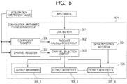
- Fig. 5 is a block diagram for explaining a configuration example of the convolution arithmetic processing circuit.
- Fig. 6 is a block diagram for explaining a configuration example of a channel selection circuit in Fig. 5 .
- the integration coefficient table is a table in which coefficients used in the convolution arithmetic operation are stored. A channel number is added to a coefficient.
- the integration coefficient table generation device 50 generates the integration coefficient table from a plurality of input coefficient tables.
- the convolution arithmetic processing circuit 101 outputs results of a plurality of number of times of convolution arithmetic operations from one convolution arithmetic operation.
- the convolution arithmetic processing circuit 101 includes a line buffer 301, a product calculation circuit 302, a channel selection circuit 303, an output control register 304, output registers 305 (a first output register 305_1, a second output register 305_2, ..., and an Nth output register 305_N), a coefficient register 306, and a channel register 307.
- the line buffer 301 acquires input image data for a specified number of lines from the semiconductor storage device 20.
- the product calculation circuit 302 calculates a product of the coefficient register 306 and an input image from the line buffer 301.
- the channel selection circuit 303 adds a channel number registered in the channel register 307 to a product calculation result, cumulatively adds the product calculation result, and outputs the product calculation result to an appropriate output register 305 according to the channel number in accordance with the output control register 304.
- the output control register 304 associates the channel number with an output register number.
- the channel selection circuit 303 includes a shift down circuit 401, a cumulative addition circuit 402, a selector circuit 403, and a cumulative addition register 404.
- the shift down circuit 401 shifts down the product calculation result by a specified number of bits and then outputs the product calculation result.
- the cumulative addition circuit 402 adds results outputted by the cumulative addition register 404 and the shift down circuit 401 for each channel and outputs the added results.
- the selector circuit 403 outputs the output of the cumulative addition circuit 402 to a specified output register 305.
- the output control register 304, the coefficient register 306, and the channel register 307 are set by the CPU 12.
- FIG. 7 is a block diagram for explaining a configuration of a 3 ⁇ 3 convolution arithmetic processing circuit.
- Fig. 8 is a schematic diagram for explaining an operation of the integration coefficient table generation device in Fig. 7 .
- Fig. 8 represents a case where the integration coefficient table generation device generates one integration coefficient table from the input coefficient tables for three channels.
- Fig. 9 is a conceptual diagram for explaining an operation of the convolution arithmetic processing circuit in Fig. 7 .
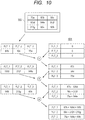
- Fig. 10 is a conceptual diagram for explaining an operation of the cumulative addition circuit in Fig. 7 .
- the convolution arithmetic processing circuit in Fig. 7 performs one 3 ⁇ 3 convolution arithmetic operation for three channels by using a 3 ⁇ 3 convolution arithmetic operation circuit.
- a coefficient of a coefficient table used in the convolution is defined as w i,j,Chanel
- the table is defined as C l,w,channel
- the following equation is established.
- C l , w , channel w 0 , 0 , channel w 0 , 1 , channel ... ... w 1 , 0 , channel w 1 , 1 , channel ... ... ⁇ ⁇ ⁇ ⁇ w 1 ⁇ 1 , w ⁇ 1 , channel
- MAX is a function that returns the maximum value of arguments .
- l i,j,FLT_A is defined as a character string that represents a type of a table used as the integration coefficient table, and the following equation is established.
- w i , j , FLT_A CHANNEL w i , j , FLT_ 1 w i , j , FLT_ 2 w i , j , FLT_ 3 .
- the integration coefficient table generation device 50 processes three types of input coefficient tables (FLT_1, FLT_2, and FLT_3) and outputs an integration coefficient table (FLT_A). Largest coefficients of those of the input coefficient tables (FLT_1, FLT_2, and FLT_3) are outputted to the integration coefficient table. Each of the largest coefficients is shaded. The maximum value of the upper left coefficients is "75" of FLT_3, the maximum value of the upper center coefficients is "87" of FLT_1, and the maximum value of the upper right coefficients is "56" of FLT_2.
- the maximum value of the middle left coefficients is "100" of FLT_1, the maximum value of the middle center coefficients is “144" of FLT_3, and the maximum value of the middle right coefficients is “212" of FLT_2.
- the maximum value of the lower left coefficients is "120" of FLT_2, the maximum value of the lower center coefficients is "60” of FLT_3, and the maximum value of the lower right coefficients is "165" of FLT_1.
- the integration coefficient table (FLT_A) where the above maximum values are integrated, the shaded portions of each of the input coefficient tables (FLT_1, FLT_2, and FLT_3) are arranged.
- the channel numbers are also stored in the integration coefficient table (FLT_A).
- the convolution arithmetic processing circuit 101 reads the coefficients and the channel numbers from the integration coefficient table and sets their values in the coefficient register 306 and the channel register 307, respectively.
- the product calculation circuit 302 calculates products of the values set in the coefficient register 306 and the values set in the line buffer 301 all at once by a 3 ⁇ 3 product calculation circuit.
- the channel selection circuit 303 sets outputs of the cumulative addition circuit 402 to the output registers 305 on the basis of the values (channel numbers) set in the channel register 307.
- the output control register 304 sets a correspondence between the output registers 305 and the channel register 307.
- the first output register 305_1 corresponds to FLT_1
- the second output register 305_2 corresponds to FLT_2
- the third output register 305_3 corresponds to FLT_3.
- the convolution arithmetic processing circuit 101 outputs results of performing a convolution arithmetic operation by using the coefficients of FLT_1, FLT_2, and FLT_3 to the first output register 305_1, the second output register 305_2, and the third output register 305_3, respectively.
- the cumulative addition circuit 402 inputs calculation results of the product calculation circuit 302 and contents of the cumulative addition register 404 for each channel on the basis of the channel numbers of the channel register 307 and adds each channel in parallel. Thereby, a cumulative addition result for each channel can be obtained at the same time.
- the convolution arithmetic processing circuit 101 separately performs cumulative addition for each channel number instead of cumulatively adding the results of the product calculation.
- the 3 ⁇ 3 convolution arithmetic operation for three channels is performed at once by using the 3 ⁇ 3 convolution arithmetic operation circuit.
- the arithmetic operation is not limited to this, and in the embodiment, it is possible to perform an N ⁇ N convolution arithmetic operation for N channels at once by using an N ⁇ N convolution arithmetic operation circuit.
- Fig. 11 is a block diagram for explaining another configuration example of the convolution arithmetic processing circuit.
- a convolution arithmetic processing circuit 101A has an input pattern register 308 and an input pattern generation circuit 309 in addition to the configuration of the convolution arithmetic processing circuit 101 of the embodiment.
- the input pattern register 308 is a register for setting how to output pixel values set in the line buffer 301 from the input pattern generation circuit 309.
- the input pattern generation circuit 309 is a circuit that receives input from the line buffer 301 and generates an output according to the input pattern register 308.
- the input pattern register 308 is set by the CPU 12.
- Fig. 12 is a diagram for explaining a configuration of a convolution arithmetic processing circuit.
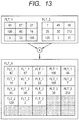
- Fig. 13 is a schematic diagram for explaining an operation of an integration coefficient table generation device in Fig. 12 .
- Fig. 13 indicates a case of generating one integration coefficient table from input coefficient tables for two channels.
- Fig. 14 is a schematic diagram for explaining an operation of an input pattern generation circuit in Fig. 12 .
- Fig. 14 indicates a case of generating a 5 ⁇ 5 input image formed from 3 ⁇ 3 input images for two channels.
- the convolution arithmetic processing circuit 101A in Fig. 12 performs two 3 ⁇ 3 convolution arithmetic operations at once by using a 5 ⁇ 5 convolution arithmetic operation circuit.
- I i,j is defined as a pixel value (gray value) of ith row and jth column of an input image
- an output of the input pattern generation circuit 309 is defined as A 5,5, and the following equation is established.
- a 5 , 5 I i , j I i + 1 , j I i + 2 , j I i + 1 , j I i + 1 , j + 1 I i + 2 , j + 1 I i , j + 2 I i + 1 , j + 2 I i + 2 , j + 2 I i , j I i + 1 , j I i + 2 , j I i + 1 , j I i + 2 , j I i + 1 , j I i + 1 , j I i + 1 , j + 1 I i + 2 , j + 1 I i + 2 , j + 1 I i + 2 , j +
- the integration coefficient table generation device 50 processes two types of input coefficient tables (FLT_1 and FLT_2) and outputs an integration coefficient table (FLT_A).
- the coefficients of the 3 ⁇ 3 input coefficient tables (FLT_1 and FLT_2) are outputted to the 5 ⁇ 5 integration coefficient table.
- the input pattern generation circuit 309 outputs pixel values in a form where the 3 ⁇ 3 pixels acquired from the line buffer 301 are repeated based on the 5 ⁇ 5 input pattern of the input pattern register 308.
- the input pattern defines an arrangement order of the first 3 ⁇ 3 pixels (1-1, 1-2, ..., and 1-9) and the second 3 ⁇ 3 pixels (2-1, 2-2, ..., and 2-9) .
- the convolution arithmetic processing circuit 101A reads the coefficients and the channel numbers from the integration coefficient table and sets their values in the coefficient register 306 and the channel register 307, respectively.
- the product calculation circuit 302 calculates products of the values set in the coefficient register 306 and the values generated by the input pattern generation circuit 309 all at once by a 5 ⁇ 5 product calculation circuit.
- the channel selection circuit 303 sets outputs of the cumulative addition circuit 402 to the output registers 305 on the basis of the values (channel numbers) set in the channel register 307.
- the output control register 304 sets a correspondence between the output registers 305 and the channel register 307.
- the first output register 305_1 corresponds to FLT_1
- the second output register 305_2 corresponds to FLT_2.
- the convolution arithmetic processing circuit 101A outputs results of performing a convolution arithmetic operation by using the coefficients of FLT_1 and FLT_2 to the first output register 305_1 and the second output register 305_2, respectively.
- the cumulative addition circuit 402 inputs calculation results of the product calculation circuit and contents of the cumulative addition register for each channel on the basis of the channel numbers of the channel register 307 and adds each channel in parallel. Thereby, a cumulative addition result for each channel can be obtained at the same time.
Landscapes
- Engineering & Computer Science (AREA)
- Physics & Mathematics (AREA)
- Theoretical Computer Science (AREA)
- General Physics & Mathematics (AREA)
- Software Systems (AREA)
- Data Mining & Analysis (AREA)
- Mathematical Physics (AREA)
- Health & Medical Sciences (AREA)
- Life Sciences & Earth Sciences (AREA)
- Biomedical Technology (AREA)
- General Engineering & Computer Science (AREA)
- Biophysics (AREA)
- Computing Systems (AREA)
- Molecular Biology (AREA)
- General Health & Medical Sciences (AREA)
- Evolutionary Computation (AREA)
- Artificial Intelligence (AREA)
- Computational Linguistics (AREA)
- Mathematical Optimization (AREA)
- Pure & Applied Mathematics (AREA)
- Computational Mathematics (AREA)
- Mathematical Analysis (AREA)
- Multimedia (AREA)
- Neurology (AREA)
- Algebra (AREA)
- Databases & Information Systems (AREA)
- Computer Vision & Pattern Recognition (AREA)
- Quality & Reliability (AREA)
- Complex Calculations (AREA)
- Image Processing (AREA)
- Image Analysis (AREA)
- Biodiversity & Conservation Biology (AREA)
Abstract
Description
- The disclosure of Japanese Patent Application No.
2017-162057 filed on August 25, 2017 - The present disclosure relates to a semiconductor device and, for example, can be applied to a semiconductor device including an image recognition device.
- Since Convolutional Neural Network (CNN) won first place in an international image classification contest (ImageNet Large Scale Visual Recognition Competition: ILSVRC) in 2012, the CNN has been used in many image recognition processes and its usefulness has been recognized. In recent years, there is a growing demand to use the CNN not only in a workstation with rich resources but also in a built-in type device. The CNN is disclosed in, for example, Japanese Unexamined Patent Application Publication No.
2008-310700 2016-99707 - However, the CNN is required to repeat a convolution arithmetic operation of an input image and coefficients the number of times corresponding to the number of channels, so that an operation amount is extremely large. Therefore, it is difficult to implement the CNN on a built-in type SoC (Silicon on Chip) whose resource is limited. The other problems and novel features will become apparent from the description of the present specification and the accompanying drawings.
- A brief outline of a typical invention of the present disclosure is as follows. A semiconductor device has a function to perform cumulative addition for each channel and performs a convolution arithmetic operation in parallel in a plurality of channels.
- According to the semiconductor device described above, it is possible to reduce the operation amount of the convolution arithmetic operation.
-
-
Fig. 1 is a diagram for explaining a concept of a convolution arithmetic operation. -
Fig. 2A is a diagram for explaining a concept of the convolution arithmetic operation. -
Fig. 2B is a diagram for explaining a concept of the convolution arithmetic operation. -
Fig. 2C is a diagram for explaining a concept of the convolution arithmetic operation. -
Fig. 3 is a diagram showing a configuration example of an image recognition system. -
Fig. 4 is a diagram showing a flow of data of the image recognition system inFig. 3 . -
Fig. 5 is a diagram for explaining a configuration example of a convolution arithmetic processing circuit inFig. 4 . -
Fig. 6 is a diagram for explaining a configuration example of a channel selection circuit inFig. 5 . -
Fig. 7 is a diagram for explaining a configuration of a 3 × 3 convolution arithmetic processing circuit. -
Fig. 8 is a schematic diagram for explaining an operation of an integration coefficient table generation device inFig. 7 . -
Fig. 9 is a conceptual diagram for explaining an operation of the convolution arithmetic processing circuit inFig. 7 . -
Fig. 10 is a conceptual diagram for explaining an operation of a cumulative addition circuit inFig. 7 . -
Fig. 11 is a diagram for explaining another configuration example of the convolution arithmetic processing circuit inFig. 4 . -
Fig. 12 is a diagram for explaining a configuration of a 5 × 5 convolution arithmetic processing circuit. -
Fig. 13 is a schematic diagram for explaining an operation of an integration coefficient table generation device inFig. 12 . -
Fig. 14 is a schematic diagram for explaining an operation of an input pattern generation circuit inFig. 12 . - First, a convolution arithmetic operation of CNN will be described with reference to
Figs. 1 and2A to 2C .Fig. 1 is a diagram for explaining a concept of the convolution arithmetic operation.Figs. 2A to 2C are diagrams for explaining a concept of the convolution arithmetic operation and are diagrams showing a product sum arithmetic operation of pixel values of an image and coefficients of a filter. - For ease of description, when an image is simplified and represented by numbers, the image can be considered as a matrix of height × width. As shown in the left of
Fig. 1 , an input image is represented by, for example, 4 × 4 binary values. A 2 × 2 filter as shown in the right ofFig. 1 is applied to such a matrix and a convolution arithmetic operation is performed. - As shown in
Fig. 2A , the filer is overlapped on a most upper left portion of the image, and values in the same positions are multiplied together. The results of the multiplication are summed up and outputted. As shown inFig. 2B , the filter is shifted horizontally by one pixel, and the values in the same positions are multiplied together in the same manner. The results of the multiplication are summed up and outputted. Thereafter, as shown inFig. 2C , the values of the filter and the input image are multiplied together and summed up until the filter reaches the lower right. - When the convolution arithmetic operation is performed, it is required that the convolution arithmetic operation of the input image and the coefficients of the filter is repeated for the number of times corresponding to the number of channels (the number of filters).
- An embodiment has a function to perform cumulative addition for each channel and performs a convolution arithmetic operation in parallel in a plurality of channels. It is possible to simultaneously and collectively perform the convolution arithmetic operation on channels, the number of which is the same as the number of blocks where the cumulative addition can be performed for each channel, so that processing time can be reduced.
- It is possible to perform the convolution arithmetic operation of a plurality of channels at one time by combining the convolution arithmetic processing circuit and an integration coefficient table. It is possible to realize the CNN by a small number of product sum arithmetic operations without performing useless product sum arithmetic operations. By using an input pattern generation circuit, it is possible to perform an arbitrary convolution arithmetic operation without depending on a filer size.
- Hereinafter, an embodiment and a modified example will be described with reference to the drawings. However, in the description below, the same components are denoted by the same reference numerals and the description thereof may be omitted.
-
Fig. 3 is a block diagram showing a configuration example of an image recognition system.Fig. 4 is a diagram showing a flow of data of the image recognition system inFig. 3 . - As shown in
Fig. 3 , animage processing system 1 includes asemiconductor device 10 and a semiconductor storage device (MEMORY) 20. Thesemiconductor device 10 includes an image recognition device (IRU) 11, a central processing unit (CPU) 12, a control circuit (MC) 13 of thesemiconductor storage device 20, and a bus that couples these, in a single semiconductor chip. Thesemiconductor storage device 20 is, for example, a DDR-SDRAM. - As shown in
Fig. 4 , an integration coefficienttable generation device 50 integrates an input coefficient table included in a pre-integration CNN model stored in a storage device, generates an integration coefficient table of a post-integration CNN model, and stores the integration coefficient table in thesemiconductor storage device 20. Theimage recognition device 11 of theimage processing system 1 processes an input image stored in thesemiconductor storage device 20 on the basis of the integration coefficient table and stores a processing result in thesemiconductor storage device 20. - The input image is an image acquired by an image pickup device (not shown in the drawings) having an optical system (lens) and an image pickup element. The input image is all or part of the image acquired by the image pickup device. The input image is stored in the
semiconductor storage device 20. - The
image recognition device 11 performs calculation by using the integration coefficient table of the post-integration CNN model and the input image and outputs a processing result. Theimage recognition device 11 is a device that performs an arithmetic operation required in the post-integration CNN model. - The processing result is an output of the
image recognition device 11. For example, the processing result is a classification result or a segmentation result of the input image or a detection result of a specific object. The processing result is stored in thesemiconductor storage device 20. - The pre-integration CNN model indicates a general CNN model. For example, the pre-integration CNN model is AlexNet, VGGNet, SegNet, or R-CNN. The input coefficient table includes coefficients used for the convolution arithmetic operation among coefficients included in the pre-integration CNN model.
- The integration coefficient
table generation device 50 is a device that analyzes the input coefficient table and generates an integration coefficient table where processing can be performed by using a smaller number of convolution arithmetic operations, and is configured by, for example, a central processing unit and a storage device that stores a program of the central processing unit and the like. - The post-integration CNN model is a model where the number of convolution arithmetic operations of the pre-integration CNN model is reduced. The integration coefficient table is an output of the integration coefficient
table generation device 50. - The
image recognition device 11 includes a convolutionarithmetic processing circuit 101, anactivation circuit 102, and apooling circuit 103, and can cumulatively add product calculation results for each channel. The convolutionarithmetic processing circuit 101 adds results of convolution arithmetic operations for each channel number corresponding to each coefficient. Theactivation circuit 102 and thepooling circuit 103 are circuits that perform activation processing and pooling processing, respectively. For the activation processing, for example, a logistic sigmoid function and a ReLU function (Rectified Linear Units), which are well known, are used. The pooling processing is a method that reduces a size of a large image while keeping important information. In the pooling processing, for example, a well-known maximum pooling function that segments an image into small windows and outputs a maximum value of data inputted from each segmented window and a well-known average pooling function that outputs an average value of inputted data are used. -
Fig. 5 is a block diagram for explaining a configuration example of the convolution arithmetic processing circuit.Fig. 6 is a block diagram for explaining a configuration example of a channel selection circuit inFig. 5 . - The integration coefficient table is a table in which coefficients used in the convolution arithmetic operation are stored. A channel number is added to a coefficient. The integration coefficient
table generation device 50 generates the integration coefficient table from a plurality of input coefficient tables. - The convolution
arithmetic processing circuit 101 outputs results of a plurality of number of times of convolution arithmetic operations from one convolution arithmetic operation. The convolutionarithmetic processing circuit 101 includes aline buffer 301, aproduct calculation circuit 302, achannel selection circuit 303, anoutput control register 304, output registers 305 (a first output register 305_1, a second output register 305_2, ..., and an Nth output register 305_N), acoefficient register 306, and achannel register 307. Theline buffer 301 acquires input image data for a specified number of lines from thesemiconductor storage device 20. Theproduct calculation circuit 302 calculates a product of thecoefficient register 306 and an input image from theline buffer 301. Thechannel selection circuit 303 adds a channel number registered in thechannel register 307 to a product calculation result, cumulatively adds the product calculation result, and outputs the product calculation result to anappropriate output register 305 according to the channel number in accordance with theoutput control register 304. The output control register 304 associates the channel number with an output register number. - As shown in
Fig. 6 , thechannel selection circuit 303 includes a shift downcircuit 401, acumulative addition circuit 402, aselector circuit 403, and acumulative addition register 404. The shift downcircuit 401 shifts down the product calculation result by a specified number of bits and then outputs the product calculation result. Thecumulative addition circuit 402 adds results outputted by thecumulative addition register 404 and the shift downcircuit 401 for each channel and outputs the added results. Theselector circuit 403 outputs the output of thecumulative addition circuit 402 to a specifiedoutput register 305. - The
output control register 304, thecoefficient register 306, and thechannel register 307 are set by theCPU 12. - An example where the integration coefficient
table generation device 50 generates one type of integration coefficient table from three types of input coefficient tables and performs the convolution arithmetic operation by using the integration coefficient table will be described with reference toFigs. 7 to 10 .Fig. 7 is a block diagram for explaining a configuration of a 3 × 3 convolution arithmetic processing circuit.Fig. 8 is a schematic diagram for explaining an operation of the integration coefficient table generation device inFig. 7 .Fig. 8 represents a case where the integration coefficient table generation device generates one integration coefficient table from the input coefficient tables for three channels.Fig. 9 is a conceptual diagram for explaining an operation of the convolution arithmetic processing circuit inFig. 7 .Fig. 10 is a conceptual diagram for explaining an operation of the cumulative addition circuit inFig. 7 . - The convolution arithmetic processing circuit in
Fig. 7 performs one 3 × 3 convolution arithmetic operation for three channels by using a 3 × 3 convolution arithmetic operation circuit. - Here, a coefficient of a coefficient table used in the convolution is defined as wi,j,Chanel, the table is defined as Cl,w,channel, and the following equation is established.

- Here, i,j represent integers, channel represents a channel number, 1 represents the width of the table, w represents the height of the table. A coefficient of the integration coefficient table is represented as follows :

- Here, MAX (...) is a function that returns the maximum value of arguments .
- Further, li,j,FLT_A is defined as a character string that represents a type of a table used as the integration coefficient table, and the following equation is established.

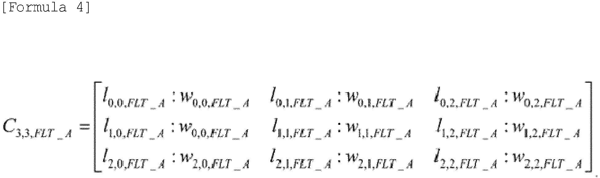
- Here, CHANNEL (...) is a function representing a channel number that returns the maximum value of arguments. At this time, C3,3,FLT_A of the integration coefficient table is represented as follows:
-
Fig. 8 schematically represents how the integration coefficient table is generated when specifically 1 = 3 and w = 3. The integration coefficienttable generation device 50 processes three types of input coefficient tables (FLT_1, FLT_2, and FLT_3) and outputs an integration coefficient table (FLT_A). Largest coefficients of those of the input coefficient tables (FLT_1, FLT_2, and FLT_3) are outputted to the integration coefficient table. Each of the largest coefficients is shaded. The maximum value of the upper left coefficients is "75" of FLT_3, the maximum value of the upper center coefficients is "87" of FLT_1, and the maximum value of the upper right coefficients is "56" of FLT_2. The maximum value of the middle left coefficients is "100" of FLT_1, the maximum value of the middle center coefficients is "144" of FLT_3, and the maximum value of the middle right coefficients is "212" of FLT_2. The maximum value of the lower left coefficients is "120" of FLT_2, the maximum value of the lower center coefficients is "60" of FLT_3, and the maximum value of the lower right coefficients is "165" of FLT_1. In the integration coefficient table (FLT_A) where the above maximum values are integrated, the shaded portions of each of the input coefficient tables (FLT_1, FLT_2, and FLT_3) are arranged. In addition to the coefficients, the channel numbers are also stored in the integration coefficient table (FLT_A). - As shown in
Fig. 8 , the convolutionarithmetic processing circuit 101 reads the coefficients and the channel numbers from the integration coefficient table and sets their values in thecoefficient register 306 and thechannel register 307, respectively. - As shown in
Fig. 9 , theproduct calculation circuit 302 calculates products of the values set in thecoefficient register 306 and the values set in theline buffer 301 all at once by a 3 × 3 product calculation circuit. Thechannel selection circuit 303 sets outputs of thecumulative addition circuit 402 to the output registers 305 on the basis of the values (channel numbers) set in thechannel register 307. The output control register 304 sets a correspondence between the output registers 305 and thechannel register 307. In this example, the first output register 305_1 corresponds to FLT_1, the second output register 305_2 corresponds to FLT_2, and the third output register 305_3 corresponds to FLT_3. The convolutionarithmetic processing circuit 101 outputs results of performing a convolution arithmetic operation by using the coefficients of FLT_1, FLT_2, and FLT_3 to the first output register 305_1, the second output register 305_2, and the third output register 305_3, respectively. - As shown in
Fig. 10 , thecumulative addition circuit 402 inputs calculation results of theproduct calculation circuit 302 and contents of the cumulative addition register 404 for each channel on the basis of the channel numbers of thechannel register 307 and adds each channel in parallel. Thereby, a cumulative addition result for each channel can be obtained at the same time. The convolutionarithmetic processing circuit 101 separately performs cumulative addition for each channel number instead of cumulatively adding the results of the product calculation. - In a specific example, an example is described where the 3 × 3 convolution arithmetic operation for three channels is performed at once by using the 3 × 3 convolution arithmetic operation circuit. However, the arithmetic operation is not limited to this, and in the embodiment, it is possible to perform an N × N convolution arithmetic operation for N channels at once by using an N × N convolution arithmetic operation circuit.
- Hereinafter, a typical modified example will be illustrated. In a description of the modified example below, the same reference numerals as those of the above embodiment may be used for portions having the same configurations and functions as those described in the above embodiment. For the descriptions of these portions, the descriptions in the above embodiment may be appropriately applied to the extent where there is no technical contradiction. Further, parts of the above embodiment and all or parts of the modified example may by appropriately and complexly applied to the extent where there is no technical contradiction.
- An example where a convolution arithmetic operation is performed regardless of an arrangement of an input image will be described with reference to
Fig. 11. Fig. 11 is a block diagram for explaining another configuration example of the convolution arithmetic processing circuit. - A convolution
arithmetic processing circuit 101A has an input pattern register 308 and an inputpattern generation circuit 309 in addition to the configuration of the convolutionarithmetic processing circuit 101 of the embodiment. The input pattern register 308 is a register for setting how to output pixel values set in theline buffer 301 from the inputpattern generation circuit 309. The inputpattern generation circuit 309 is a circuit that receives input from theline buffer 301 and generates an output according to theinput pattern register 308. The input pattern register 308 is set by theCPU 12. - Next, an example where the integration coefficient
table generation device 50 generates one type of integration coefficient table from two types of input coefficient tables and performs the convolution arithmetic operation by using the integration coefficient table will be described with reference toFigs. 12 to 14 .Fig. 12 is a diagram for explaining a configuration of a convolution arithmetic processing circuit.Fig. 13 is a schematic diagram for explaining an operation of an integration coefficient table generation device inFig. 12 .Fig. 13 indicates a case of generating one integration coefficient table from input coefficient tables for two channels.Fig. 14 is a schematic diagram for explaining an operation of an input pattern generation circuit inFig. 12 .Fig. 14 indicates a case of generating a 5 × 5 input image formed from 3 × 3 input images for two channels. - The convolution
arithmetic processing circuit 101A inFig. 12 performs two 3 × 3 convolution arithmetic operations at once by using a 5 × 5 convolution arithmetic operation circuit. - When the input coefficient tables are C3,3,FLT_1 and C3,3,FLT_2, and the integration coefficient table is C5,5,FLT_A, the following equation is established.

- Further, Ii,j is defined as a pixel value (gray value) of ith row and jth column of an input image, an output of the input
pattern generation circuit 309 is defined as A5,5, and the following equation is established.
-
Fig. 13 schematically shows how the integration coefficient table is generated when specifically 1 = 3 and w = 3. The integration coefficienttable generation device 50 processes two types of input coefficient tables (FLT_1 and FLT_2) and outputs an integration coefficient table (FLT_A). The coefficients of the 3 × 3 input coefficient tables (FLT_1 and FLT_2) are outputted to the 5 × 5 integration coefficient table. - As shown in
Fig. 13 , from left to right of the first row of FLT_A, coefficients "40", "87", and "21" in the first row of FLT_1 and coefficients "100" and "45" in the second row of FLT_1 are arranged. From left to right of the second row of FLT_A, the right end coefficient "14" in the second row of FLT_1, coefficients "9", "33" and "165" in the third row of FLT_1, and the left end coefficient "7" in the first row of FLT_2 are arranged. From left to right of the third row of FLT_A, the center coefficient "45" and the right end coefficient "56" in the first row ofFLT 2 and coefficients "25", "30", and "212" in the second row of FLT_2 are arranged. From left to right of the fourth row of FLT_A, coefficients "120", "2", and "27" in the third row of FLT_2 are arranged. No coefficient is arranged in the right two positions in the fourth row of FLT_A and all positions in the fifth row of FLT_A, and these positions become blank spaces. In addition to the coefficients, the channel numbers are also stored in the integration coefficient table (FLT_A). - As shown in
Fig. 14 , the inputpattern generation circuit 309 outputs pixel values in a form where the 3 × 3 pixels acquired from theline buffer 301 are repeated based on the 5 × 5 input pattern of theinput pattern register 308. The input pattern defines an arrangement order of the first 3 × 3 pixels (1-1, 1-2, ..., and 1-9) and the second 3 × 3 pixels (2-1, 2-2, ..., and 2-9) . - As shown in
Fig. 14 , from left to right of the first row of the output of the inputpattern generation circuit 309, pixel values "76", "120", and "32" in the first row of an input image and pixel values "77" and "130" in the second row of the input image are arranged. From left to right of the second row, the right end pixel value "34" in the second row of the input image, pixel values "130", "100", and "54" in the third row of the input image, and the left end pixel value "78" in the first row of the second input image are arranged. From left to right of the third row, the center pixel value "120" and the right end pixel value "32" in the first row of the input image and pixel values "77", "130", and "34" in the second row of the input image are arranged. From left to right of the fourth row, pixel values "130", "110", and "54" in the third row of the input image are arranged. No pixel is arranged in the right two positions in the fourth row and all positions in the fifth row, and these positions become blank spaces. Thereby, the arrangement of the pixels of the output of the inputpattern generation circuit 309 is the same as the arrangement of the coefficients of the integration coefficient table (FLT_A). - It is possible to read the pixels stored in the
line buffer 301 in an arbitrary form by adding the input pattern register 308 and the inputpattern generation circuit 309. - In the same manner as in the embodiment, the convolution
arithmetic processing circuit 101A reads the coefficients and the channel numbers from the integration coefficient table and sets their values in thecoefficient register 306 and thechannel register 307, respectively. - In a manner similar to that in the embodiment, the
product calculation circuit 302 calculates products of the values set in thecoefficient register 306 and the values generated by the inputpattern generation circuit 309 all at once by a 5 × 5 product calculation circuit. Thechannel selection circuit 303 sets outputs of thecumulative addition circuit 402 to the output registers 305 on the basis of the values (channel numbers) set in thechannel register 307. The output control register 304 sets a correspondence between the output registers 305 and thechannel register 307. In this example, the first output register 305_1 corresponds to FLT_1 and the second output register 305_2 corresponds to FLT_2. The convolutionarithmetic processing circuit 101A outputs results of performing a convolution arithmetic operation by using the coefficients of FLT_1 and FLT_2 to the first output register 305_1 and the second output register 305_2, respectively. In the same manner as in the embodiment, thecumulative addition circuit 402 inputs calculation results of the product calculation circuit and contents of the cumulative addition register for each channel on the basis of the channel numbers of thechannel register 307 and adds each channel in parallel. Thereby, a cumulative addition result for each channel can be obtained at the same time. - In the modified example, it is possible to perform an arbitrary convolution arithmetic operation by using the input pattern register 308 and the integration coefficient
table generation device 50 in combination with each other. Therefore, even when a 5 × 5 convolution arithmetic operation circuit is used, it is possible to efficiently perform a 3 × 3 or 1 × 1 convolution arithmetic operation. - In a specific example, an example is described where two 3 × 3 convolution arithmetic operations are performed at once by using the 5 × 5 convolution arithmetic operation circuit. However, the arithmetic operation is not limited to this, and in the modified example, it is possible to perform L number of M × M convolution arithmetic operations at once by using an N × N convolution arithmetic operation circuit. Here, M < N and L = INT (N2/M2) ≥ 2.
- While the invention made by the inventors has been specifically described based on the embodiment and the modified example, it is needless to say that the present invention is not limited to the embodiment and the modified example and may be variously modified.
Claims (15)
- A semiconductor device comprising:an image recognition device having a convolution arithmetic processing circuit,wherein the convolution arithmetic processing circuit includesa coefficient register where coefficients of an integration coefficient table are set,a product calculation circuit that calculates products of an input image and the coefficients,a channel register where a channel number of the integration coefficient table is set,a channel selection circuit that selects an output destination of a cumulative addition arithmetic operation on the basis of the channel number, anda plurality of output registers that store a result of the cumulative addition arithmetic operation,wherein the integration coefficient table is a table where a plurality of input coefficient tables are integrated and the integration coefficient table has a size of N × N, andwherein the product calculation circuit can calculate data of N × N all at once.
- The semiconductor device according to claim 1,wherein the channel selection circuit includesa cumulative addition circuit that adds the products for each channel number, anda cumulative addition register that holds an output of the cumulative addition circuit for each channel number, andwherein the cumulative addition circuit performs the addition for each channel number in parallel.
- The semiconductor device according to claim 1 or 2,
wherein the channel selection circuit further includes a selector that outputs the output of the cumulative addition circuit to any one of the output registers on the basis of the channel number. - The semiconductor device according to one of claims 1 to 3,
wherein in each element of the integration coefficient table, a coefficient having a largest value among coefficients in each corresponding element in the input coefficient tables is stored. - The semiconductor device according to one of claims 1 to 4,
wherein the number of the input coefficient tables is N and each of the input coefficient tables has a size of N × N. - The semiconductor device according to one of claims 1 to 5, further comprising:an input pattern register; andan input pattern generation circuit that changes an arrangement of an input image based on content of the input pattern register,wherein the integration coefficient table is a table where L input coefficient tables are integrated, the integration coefficient table has a size of N × N, each of the L input coefficient tables has a size of M × M, and M is a value smaller than N, andwherein the product calculation circuit can calculate data of N × N all at once.
- The semiconductor device according to claim 6,wherein the channel selection circuit includesa cumulative addition circuit that adds the products for each channel number, anda cumulative addition register that holds an output of the cumulative addition circuit for each channel number, andwherein the cumulative addition circuit performs the addition for each channel number in parallel.
- The semiconductor device according to claim 7,
wherein the channel selection circuit further includes a selector that outputs the output of the cumulative addition circuit to any one of the output registers on the basis of the channel number. - The semiconductor device according to claim 6,
wherein the input pattern generation circuit repeats an input image of M × M L times and converts the L input images of M × M into an input image of N × N. - An image recognition system comprising:a semiconductor device; anda semiconductor storage device,wherein the semiconductor device includesa convolution arithmetic processing circuit including a coefficient register where coefficients of an integration coefficient table are set, a product calculation circuit that calculates products of an input image read from the semiconductor storage device and the coefficients, a channel register where a channel number of the integration coefficient table is set, a channel selection circuit that selects an output destination of a cumulative addition arithmetic operation on the basis of the channel number, and a plurality of output registers that store a result of the cumulative addition arithmetic operation, anda pooling circuit,wherein the product calculation circuit can calculate data of N × N all at once, andwherein the integration coefficient table is a table where a plurality of input coefficient tables are integrated and the integration coefficient table has a size of N × N.
- The image recognition system according to claim 10,wherein the channel selection circuit includesa cumulative addition circuit that adds the products for each channel number, anda cumulative addition register that holds an output of the cumulative addition circuit for each channel number, andwherein the cumulative addition circuit performs the addition for each channel number in parallel.
- The image recognition system according to claim 10 or 11,
wherein the channel selection circuit further includes a selector that outputs the output of the cumulative addition circuit to any one of the output registers on the basis of the channel number. - The image recognition system according to claim 10, 11, or 12,
wherein in each element of the integration coefficient table, a coefficient having a largest value among coefficients in each corresponding element in the input coefficient tables is stored. - The image recognition system according to one of claims 10 to 13,wherein the semiconductor device further includesan input pattern register, andan input pattern generation circuit that changes an arrangement of an input image based on content of the input pattern register,wherein the integration coefficient table is a table where L input coefficient tables are integrated, the integration coefficient table has a size of N × N, each of the L input coefficient tables has a size of M × M, and M is a value smaller than N, andwherein the product calculation circuit can calculate data of N × N all at once.
- The image recognition system according to one of claims 10 to 14, further comprising the features as additionally defined in one or more of claims 2, 3, 4, 5, or 9.
Applications Claiming Priority (1)
| Application Number | Priority Date | Filing Date | Title |
|---|---|---|---|
| JP2017162057A JP2019040403A (en) | 2017-08-25 | 2017-08-25 | Semiconductor device and image recognition system |
Publications (2)
| Publication Number | Publication Date |
|---|---|
| EP3447682A1 true EP3447682A1 (en) | 2019-02-27 |
| EP3447682B1 EP3447682B1 (en) | 2023-05-24 |
Family
ID=63041921
Family Applications (1)
| Application Number | Title | Priority Date | Filing Date |
|---|---|---|---|
| EP18185295.5A Active EP3447682B1 (en) | 2017-08-25 | 2018-07-24 | Semiconductor device and image recognition system |
Country Status (5)
| Country | Link |
|---|---|
| US (1) | US11461633B2 (en) |
| EP (1) | EP3447682B1 (en) |
| JP (1) | JP2019040403A (en) |
| CN (1) | CN109427035B (en) |
| TW (1) | TW201921287A (en) |
Families Citing this family (5)
| Publication number | Priority date | Publication date | Assignee | Title |
|---|---|---|---|---|
| JP7435602B2 (en) * | 2019-05-10 | 2024-02-21 | ソニーグループ株式会社 | Computing equipment and computing systems |
| US20220398441A1 (en) | 2021-06-11 | 2022-12-15 | Renesas Electronics Corporation | Semiconductor device |
| JP7801882B2 (en) | 2021-11-22 | 2026-01-19 | ルネサスエレクトロニクス株式会社 | Semiconductor Devices |
| JP7719033B2 (en) | 2022-05-18 | 2025-08-05 | ルネサスエレクトロニクス株式会社 | Semiconductor Devices |
| JP2024179184A (en) | 2023-06-14 | 2024-12-26 | ルネサスエレクトロニクス株式会社 | Semiconductor Device |
Citations (5)
| Publication number | Priority date | Publication date | Assignee | Title |
|---|---|---|---|---|
| JP2008310700A (en) | 2007-06-15 | 2008-12-25 | Canon Inc | Arithmetic processing apparatus and method |
| US20140337262A1 (en) * | 2008-12-04 | 2014-11-13 | Canon Kabushiki Kaisha | Convolution operation circuit and object recognition apparatus |
| JP2016099707A (en) | 2014-11-19 | 2016-05-30 | 株式会社デンソー | Arithmetic processing unit |
| US20160379073A1 (en) * | 2015-06-24 | 2016-12-29 | Qualcomm Incorporated | Systems and methods for image processing in a deep convolution network |
| US20170116495A1 (en) * | 2015-10-21 | 2017-04-27 | Canon Kabushiki Kaisha | Convolution operation apparatus |
Family Cites Families (3)
| Publication number | Priority date | Publication date | Assignee | Title |
|---|---|---|---|---|
| AUPQ289099A0 (en) * | 1999-09-16 | 1999-10-07 | Silverbrook Research Pty Ltd | Method and apparatus for manipulating a bayer image |
| CN108073549B (en) * | 2016-11-14 | 2021-04-27 | 耐能股份有限公司 | Convolution operation device and method |
| CN106951395B (en) * | 2017-02-13 | 2018-08-17 | 上海客鹭信息技术有限公司 | Parallel convolution operations method and device towards compression convolutional neural networks |
-
2017
- 2017-08-25 JP JP2017162057A patent/JP2019040403A/en active Pending
-
2018
- 2018-07-13 US US16/035,010 patent/US11461633B2/en active Active
- 2018-07-24 EP EP18185295.5A patent/EP3447682B1/en active Active
- 2018-08-03 TW TW107126993A patent/TW201921287A/en unknown
- 2018-08-17 CN CN201810938920.6A patent/CN109427035B/en active Active
Patent Citations (5)
| Publication number | Priority date | Publication date | Assignee | Title |
|---|---|---|---|---|
| JP2008310700A (en) | 2007-06-15 | 2008-12-25 | Canon Inc | Arithmetic processing apparatus and method |
| US20140337262A1 (en) * | 2008-12-04 | 2014-11-13 | Canon Kabushiki Kaisha | Convolution operation circuit and object recognition apparatus |
| JP2016099707A (en) | 2014-11-19 | 2016-05-30 | 株式会社デンソー | Arithmetic processing unit |
| US20160379073A1 (en) * | 2015-06-24 | 2016-12-29 | Qualcomm Incorporated | Systems and methods for image processing in a deep convolution network |
| US20170116495A1 (en) * | 2015-10-21 | 2017-04-27 | Canon Kabushiki Kaisha | Convolution operation apparatus |
Non-Patent Citations (2)
| Title |
|---|
| ARAVIND VASUDEVAN ET AL: "Parallel Multi Channel convolution using General Matrix Multiplication", 2017 IEEE 28TH INTERNATIONAL CONFERENCE ON APPLICATION-SPECIFIC SYSTEMS, ARCHITECTURES AND PROCESSORS (ASAP), 1 July 2017 (2017-07-01), pages 19 - 24, XP055532189, ISBN: 978-1-5090-4825-0, DOI: 10.1109/ASAP.2017.7995254 * |
| JAMES GARLAND ET AL: "Low Complexity Multiply Accumulate Unit for Weight-Sharing Convolutional Neural Networks", IEEE COMPUTER ARCHITECTURE LETTERS, vol. 16, no. 2, 1 July 2017 (2017-07-01), US, pages 132 - 135, XP055532198, ISSN: 1556-6056, DOI: 10.1109/LCA.2017.2656880 * |
Also Published As
| Publication number | Publication date |
|---|---|
| TW201921287A (en) | 2019-06-01 |
| US11461633B2 (en) | 2022-10-04 |
| JP2019040403A (en) | 2019-03-14 |
| US20190065947A1 (en) | 2019-02-28 |
| CN109427035B (en) | 2023-09-05 |
| EP3447682B1 (en) | 2023-05-24 |
| CN109427035A (en) | 2019-03-05 |
Similar Documents
| Publication | Publication Date | Title |
|---|---|---|
| EP3447682B1 (en) | Semiconductor device and image recognition system | |
| US10824934B2 (en) | Methods and apparatus for matrix processing in a convolutional neural network | |
| US11562046B2 (en) | Neural network processor using dyadic weight matrix and operation method thereof | |
| US11501146B2 (en) | Convolutional neural network | |
| US20200005074A1 (en) | Semantic image segmentation using gated dense pyramid blocks | |
| US10558386B2 (en) | Operation device and operation system | |
| US11537438B2 (en) | Information processing apparatus, information processing method, and storage medium for efficient storage of kernels of various sizes | |
| US11281746B2 (en) | Arithmetic operation circuit, arithmetic operation method, and program | |
| US20210004701A1 (en) | Inference device, convolution computation method and program | |
| US20200394516A1 (en) | Filter processing device and method of performing convolution operation at filter processing device | |
| US20220044053A1 (en) | Semantic image segmentation using gated dense pyramid blocks | |
| KR20200062014A (en) | Apparatus for accelerating neural network using weight with dyadic matrix form and operation method thereof | |
| US20160283801A1 (en) | Image recognition method, image recognition device and image recognition program | |
| CN112633260A (en) | Video motion classification method and device, readable storage medium and equipment | |
| CN113610704A (en) | Image generation method, device, equipment and readable storage medium | |
| WO2023122896A1 (en) | Data processing method and apparatus | |
| US20210287070A1 (en) | Data processing apparatus, data processing method, and non-transitory computer-readable storage medium | |
| US7212685B2 (en) | Method for processing image data of optical mouse | |
| US12333405B2 (en) | Methods and apparatus for matrix processing in a convolutional neural network | |
| CN111179212A (en) | Method for realizing micro target detection chip integrating distillation strategy and deconvolution | |
| EP3680827B1 (en) | Information processing apparatus and memory control method | |
| US20210295142A1 (en) | Image processing apparatus | |
| US11625224B2 (en) | Apparatus and method using neural network | |
| EP4325397A1 (en) | Information processing apparatus, information processing method, and computer-readable storage medium | |
| JP6848673B2 (en) | Arithmetic processing unit |
Legal Events
| Date | Code | Title | Description |
|---|---|---|---|
| PUAI | Public reference made under article 153(3) epc to a published international application that has entered the european phase |
Free format text: ORIGINAL CODE: 0009012 |
|
| STAA | Information on the status of an ep patent application or granted ep patent |
Free format text: STATUS: THE APPLICATION HAS BEEN PUBLISHED |
|
| AK | Designated contracting states |
Kind code of ref document: A1 Designated state(s): AL AT BE BG CH CY CZ DE DK EE ES FI FR GB GR HR HU IE IS IT LI LT LU LV MC MK MT NL NO PL PT RO RS SE SI SK SM TR |
|
| AX | Request for extension of the european patent |
Extension state: BA ME |
|
| STAA | Information on the status of an ep patent application or granted ep patent |
Free format text: STATUS: REQUEST FOR EXAMINATION WAS MADE |
|
| 17P | Request for examination filed |
Effective date: 20190827 |
|
| RBV | Designated contracting states (corrected) |
Designated state(s): AL AT BE BG CH CY CZ DE DK EE ES FI FR GB GR HR HU IE IS IT LI LT LU LV MC MK MT NL NO PL PT RO RS SE SI SK SM TR |
|
| STAA | Information on the status of an ep patent application or granted ep patent |
Free format text: STATUS: EXAMINATION IS IN PROGRESS |
|
| 17Q | First examination report despatched |
Effective date: 20191128 |
|
| REG | Reference to a national code |
Ref country code: DE Ref legal event code: R079 Ref document number: 602018050111 Country of ref document: DE Free format text: PREVIOUS MAIN CLASS: G06K0009000000 Ipc: G06V0010940000 |
|
| GRAP | Despatch of communication of intention to grant a patent |
Free format text: ORIGINAL CODE: EPIDOSNIGR1 |
|
| STAA | Information on the status of an ep patent application or granted ep patent |
Free format text: STATUS: GRANT OF PATENT IS INTENDED |
|
| RIC1 | Information provided on ipc code assigned before grant |
Ipc: G06N 3/04 20060101ALN20221208BHEP Ipc: G06F 17/15 20060101ALN20221208BHEP Ipc: G06N 3/063 20060101ALN20221208BHEP Ipc: G06V 10/94 20220101AFI20221208BHEP |
|
| INTG | Intention to grant announced |
Effective date: 20230104 |
|
| GRAS | Grant fee paid |
Free format text: ORIGINAL CODE: EPIDOSNIGR3 |
|
| GRAA | (expected) grant |
Free format text: ORIGINAL CODE: 0009210 |
|
| STAA | Information on the status of an ep patent application or granted ep patent |
Free format text: STATUS: THE PATENT HAS BEEN GRANTED |
|
| AK | Designated contracting states |
Kind code of ref document: B1 Designated state(s): AL AT BE BG CH CY CZ DE DK EE ES FI FR GB GR HR HU IE IS IT LI LT LU LV MC MK MT NL NO PL PT RO RS SE SI SK SM TR |
|
| REG | Reference to a national code |
Ref country code: GB Ref legal event code: FG4D |
|
| REG | Reference to a national code |
Ref country code: CH Ref legal event code: EP |
|
| REG | Reference to a national code |
Ref country code: DE Ref legal event code: R096 Ref document number: 602018050111 Country of ref document: DE |
|
| REG | Reference to a national code |
Ref country code: AT Ref legal event code: REF Ref document number: 1570013 Country of ref document: AT Kind code of ref document: T Effective date: 20230615 |
|
| REG | Reference to a national code |
Ref country code: IE Ref legal event code: FG4D |
|
| REG | Reference to a national code |
Ref country code: LT Ref legal event code: MG9D |
|
| REG | Reference to a national code |
Ref country code: NL Ref legal event code: MP Effective date: 20230524 |
|
| REG | Reference to a national code |
Ref country code: AT Ref legal event code: MK05 Ref document number: 1570013 Country of ref document: AT Kind code of ref document: T Effective date: 20230524 |
|
| PG25 | Lapsed in a contracting state [announced via postgrant information from national office to epo] |
Ref country code: SE Free format text: LAPSE BECAUSE OF FAILURE TO SUBMIT A TRANSLATION OF THE DESCRIPTION OR TO PAY THE FEE WITHIN THE PRESCRIBED TIME-LIMIT Effective date: 20230524 Ref country code: PT Free format text: LAPSE BECAUSE OF FAILURE TO SUBMIT A TRANSLATION OF THE DESCRIPTION OR TO PAY THE FEE WITHIN THE PRESCRIBED TIME-LIMIT Effective date: 20230925 Ref country code: NO Free format text: LAPSE BECAUSE OF FAILURE TO SUBMIT A TRANSLATION OF THE DESCRIPTION OR TO PAY THE FEE WITHIN THE PRESCRIBED TIME-LIMIT Effective date: 20230824 Ref country code: NL Free format text: LAPSE BECAUSE OF FAILURE TO SUBMIT A TRANSLATION OF THE DESCRIPTION OR TO PAY THE FEE WITHIN THE PRESCRIBED TIME-LIMIT Effective date: 20230524 Ref country code: ES Free format text: LAPSE BECAUSE OF FAILURE TO SUBMIT A TRANSLATION OF THE DESCRIPTION OR TO PAY THE FEE WITHIN THE PRESCRIBED TIME-LIMIT Effective date: 20230524 Ref country code: AT Free format text: LAPSE BECAUSE OF FAILURE TO SUBMIT A TRANSLATION OF THE DESCRIPTION OR TO PAY THE FEE WITHIN THE PRESCRIBED TIME-LIMIT Effective date: 20230524 |
|
| PG25 | Lapsed in a contracting state [announced via postgrant information from national office to epo] |
Ref country code: RS Free format text: LAPSE BECAUSE OF FAILURE TO SUBMIT A TRANSLATION OF THE DESCRIPTION OR TO PAY THE FEE WITHIN THE PRESCRIBED TIME-LIMIT Effective date: 20230524 Ref country code: PL Free format text: LAPSE BECAUSE OF FAILURE TO SUBMIT A TRANSLATION OF THE DESCRIPTION OR TO PAY THE FEE WITHIN THE PRESCRIBED TIME-LIMIT Effective date: 20230524 Ref country code: LV Free format text: LAPSE BECAUSE OF FAILURE TO SUBMIT A TRANSLATION OF THE DESCRIPTION OR TO PAY THE FEE WITHIN THE PRESCRIBED TIME-LIMIT Effective date: 20230524 Ref country code: LT Free format text: LAPSE BECAUSE OF FAILURE TO SUBMIT A TRANSLATION OF THE DESCRIPTION OR TO PAY THE FEE WITHIN THE PRESCRIBED TIME-LIMIT Effective date: 20230524 Ref country code: IS Free format text: LAPSE BECAUSE OF FAILURE TO SUBMIT A TRANSLATION OF THE DESCRIPTION OR TO PAY THE FEE WITHIN THE PRESCRIBED TIME-LIMIT Effective date: 20230924 Ref country code: HR Free format text: LAPSE BECAUSE OF FAILURE TO SUBMIT A TRANSLATION OF THE DESCRIPTION OR TO PAY THE FEE WITHIN THE PRESCRIBED TIME-LIMIT Effective date: 20230524 Ref country code: GR Free format text: LAPSE BECAUSE OF FAILURE TO SUBMIT A TRANSLATION OF THE DESCRIPTION OR TO PAY THE FEE WITHIN THE PRESCRIBED TIME-LIMIT Effective date: 20230825 |
|
| PG25 | Lapsed in a contracting state [announced via postgrant information from national office to epo] |
Ref country code: FI Free format text: LAPSE BECAUSE OF FAILURE TO SUBMIT A TRANSLATION OF THE DESCRIPTION OR TO PAY THE FEE WITHIN THE PRESCRIBED TIME-LIMIT Effective date: 20230524 |
|
| PG25 | Lapsed in a contracting state [announced via postgrant information from national office to epo] |
Ref country code: SK Free format text: LAPSE BECAUSE OF FAILURE TO SUBMIT A TRANSLATION OF THE DESCRIPTION OR TO PAY THE FEE WITHIN THE PRESCRIBED TIME-LIMIT Effective date: 20230524 |
|
| PG25 | Lapsed in a contracting state [announced via postgrant information from national office to epo] |
Ref country code: SM Free format text: LAPSE BECAUSE OF FAILURE TO SUBMIT A TRANSLATION OF THE DESCRIPTION OR TO PAY THE FEE WITHIN THE PRESCRIBED TIME-LIMIT Effective date: 20230524 Ref country code: SK Free format text: LAPSE BECAUSE OF FAILURE TO SUBMIT A TRANSLATION OF THE DESCRIPTION OR TO PAY THE FEE WITHIN THE PRESCRIBED TIME-LIMIT Effective date: 20230524 Ref country code: RO Free format text: LAPSE BECAUSE OF FAILURE TO SUBMIT A TRANSLATION OF THE DESCRIPTION OR TO PAY THE FEE WITHIN THE PRESCRIBED TIME-LIMIT Effective date: 20230524 Ref country code: EE Free format text: LAPSE BECAUSE OF FAILURE TO SUBMIT A TRANSLATION OF THE DESCRIPTION OR TO PAY THE FEE WITHIN THE PRESCRIBED TIME-LIMIT Effective date: 20230524 Ref country code: DK Free format text: LAPSE BECAUSE OF FAILURE TO SUBMIT A TRANSLATION OF THE DESCRIPTION OR TO PAY THE FEE WITHIN THE PRESCRIBED TIME-LIMIT Effective date: 20230524 Ref country code: CZ Free format text: LAPSE BECAUSE OF FAILURE TO SUBMIT A TRANSLATION OF THE DESCRIPTION OR TO PAY THE FEE WITHIN THE PRESCRIBED TIME-LIMIT Effective date: 20230524 |
|
| REG | Reference to a national code |
Ref country code: DE Ref legal event code: R097 Ref document number: 602018050111 Country of ref document: DE |
|
| PG25 | Lapsed in a contracting state [announced via postgrant information from national office to epo] |
Ref country code: MC Free format text: LAPSE BECAUSE OF FAILURE TO SUBMIT A TRANSLATION OF THE DESCRIPTION OR TO PAY THE FEE WITHIN THE PRESCRIBED TIME-LIMIT Effective date: 20230524 |
|
| PG25 | Lapsed in a contracting state [announced via postgrant information from national office to epo] |
Ref country code: MC Free format text: LAPSE BECAUSE OF FAILURE TO SUBMIT A TRANSLATION OF THE DESCRIPTION OR TO PAY THE FEE WITHIN THE PRESCRIBED TIME-LIMIT Effective date: 20230524 |
|
| REG | Reference to a national code |
Ref country code: CH Ref legal event code: PL |
|
| REG | Reference to a national code |
Ref country code: BE Ref legal event code: MM Effective date: 20230731 |
|
| PG25 | Lapsed in a contracting state [announced via postgrant information from national office to epo] |
Ref country code: LU Free format text: LAPSE BECAUSE OF NON-PAYMENT OF DUE FEES Effective date: 20230724 |
|
| PG25 | Lapsed in a contracting state [announced via postgrant information from national office to epo] |
Ref country code: LU Free format text: LAPSE BECAUSE OF NON-PAYMENT OF DUE FEES Effective date: 20230724 |
|
| PLBE | No opposition filed within time limit |
Free format text: ORIGINAL CODE: 0009261 |
|
| STAA | Information on the status of an ep patent application or granted ep patent |
Free format text: STATUS: NO OPPOSITION FILED WITHIN TIME LIMIT |
|
| GBPC | Gb: european patent ceased through non-payment of renewal fee |
Effective date: 20230824 |
|
| REG | Reference to a national code |
Ref country code: IE Ref legal event code: MM4A |
|
| PG25 | Lapsed in a contracting state [announced via postgrant information from national office to epo] |
Ref country code: CH Free format text: LAPSE BECAUSE OF NON-PAYMENT OF DUE FEES Effective date: 20230731 |
|
| 26N | No opposition filed |
Effective date: 20240227 |
|
| PG25 | Lapsed in a contracting state [announced via postgrant information from national office to epo] |
Ref country code: SI Free format text: LAPSE BECAUSE OF FAILURE TO SUBMIT A TRANSLATION OF THE DESCRIPTION OR TO PAY THE FEE WITHIN THE PRESCRIBED TIME-LIMIT Effective date: 20230524 |
|
| PG25 | Lapsed in a contracting state [announced via postgrant information from national office to epo] |
Ref country code: SI Free format text: LAPSE BECAUSE OF FAILURE TO SUBMIT A TRANSLATION OF THE DESCRIPTION OR TO PAY THE FEE WITHIN THE PRESCRIBED TIME-LIMIT Effective date: 20230524 Ref country code: IT Free format text: LAPSE BECAUSE OF FAILURE TO SUBMIT A TRANSLATION OF THE DESCRIPTION OR TO PAY THE FEE WITHIN THE PRESCRIBED TIME-LIMIT Effective date: 20230524 Ref country code: FR Free format text: LAPSE BECAUSE OF NON-PAYMENT OF DUE FEES Effective date: 20230724 Ref country code: BE Free format text: LAPSE BECAUSE OF NON-PAYMENT OF DUE FEES Effective date: 20230731 |
|
| PG25 | Lapsed in a contracting state [announced via postgrant information from national office to epo] |
Ref country code: IE Free format text: LAPSE BECAUSE OF NON-PAYMENT OF DUE FEES Effective date: 20230724 |
|
| PG25 | Lapsed in a contracting state [announced via postgrant information from national office to epo] |
Ref country code: GB Free format text: LAPSE BECAUSE OF NON-PAYMENT OF DUE FEES Effective date: 20230824 |
|
| PG25 | Lapsed in a contracting state [announced via postgrant information from national office to epo] |
Ref country code: IE Free format text: LAPSE BECAUSE OF NON-PAYMENT OF DUE FEES Effective date: 20230724 Ref country code: GB Free format text: LAPSE BECAUSE OF NON-PAYMENT OF DUE FEES Effective date: 20230824 |
|
| PG25 | Lapsed in a contracting state [announced via postgrant information from national office to epo] |
Ref country code: BG Free format text: LAPSE BECAUSE OF FAILURE TO SUBMIT A TRANSLATION OF THE DESCRIPTION OR TO PAY THE FEE WITHIN THE PRESCRIBED TIME-LIMIT Effective date: 20230524 |
|
| PG25 | Lapsed in a contracting state [announced via postgrant information from national office to epo] |
Ref country code: BG Free format text: LAPSE BECAUSE OF FAILURE TO SUBMIT A TRANSLATION OF THE DESCRIPTION OR TO PAY THE FEE WITHIN THE PRESCRIBED TIME-LIMIT Effective date: 20230524 |
|
| PG25 | Lapsed in a contracting state [announced via postgrant information from national office to epo] |
Ref country code: CY Free format text: LAPSE BECAUSE OF FAILURE TO SUBMIT A TRANSLATION OF THE DESCRIPTION OR TO PAY THE FEE WITHIN THE PRESCRIBED TIME-LIMIT; INVALID AB INITIO Effective date: 20180724 |
|
| PG25 | Lapsed in a contracting state [announced via postgrant information from national office to epo] |
Ref country code: HU Free format text: LAPSE BECAUSE OF FAILURE TO SUBMIT A TRANSLATION OF THE DESCRIPTION OR TO PAY THE FEE WITHIN THE PRESCRIBED TIME-LIMIT; INVALID AB INITIO Effective date: 20180724 |
|
| PGFP | Annual fee paid to national office [announced via postgrant information from national office to epo] |
Ref country code: DE Payment date: 20250728 Year of fee payment: 8 |
|
| PG25 | Lapsed in a contracting state [announced via postgrant information from national office to epo] |
Ref country code: TR Free format text: LAPSE BECAUSE OF FAILURE TO SUBMIT A TRANSLATION OF THE DESCRIPTION OR TO PAY THE FEE WITHIN THE PRESCRIBED TIME-LIMIT Effective date: 20230524 |