EP3447566A1 - Light control film, laminated glass and method for producing light control film - Google Patents
Light control film, laminated glass and method for producing light control film Download PDFInfo
- Publication number
- EP3447566A1 EP3447566A1 EP17786029.3A EP17786029A EP3447566A1 EP 3447566 A1 EP3447566 A1 EP 3447566A1 EP 17786029 A EP17786029 A EP 17786029A EP 3447566 A1 EP3447566 A1 EP 3447566A1
- Authority
- EP
- European Patent Office
- Prior art keywords
- laminate
- spacer
- liquid crystal
- producing
- light control
- Prior art date
- Legal status (The legal status is an assumption and is not a legal conclusion. Google has not performed a legal analysis and makes no representation as to the accuracy of the status listed.)
- Granted
Links
Images



Classifications
-
- G—PHYSICS
- G02—OPTICS
- G02F—OPTICAL DEVICES OR ARRANGEMENTS FOR THE CONTROL OF LIGHT BY MODIFICATION OF THE OPTICAL PROPERTIES OF THE MEDIA OF THE ELEMENTS INVOLVED THEREIN; NON-LINEAR OPTICS; FREQUENCY-CHANGING OF LIGHT; OPTICAL LOGIC ELEMENTS; OPTICAL ANALOGUE/DIGITAL CONVERTERS
- G02F1/00—Devices or arrangements for the control of the intensity, colour, phase, polarisation or direction of light arriving from an independent light source, e.g. switching, gating or modulating; Non-linear optics
- G02F1/01—Devices or arrangements for the control of the intensity, colour, phase, polarisation or direction of light arriving from an independent light source, e.g. switching, gating or modulating; Non-linear optics for the control of the intensity, phase, polarisation or colour
- G02F1/13—Devices or arrangements for the control of the intensity, colour, phase, polarisation or direction of light arriving from an independent light source, e.g. switching, gating or modulating; Non-linear optics for the control of the intensity, phase, polarisation or colour based on liquid crystals, e.g. single liquid crystal display cells
- G02F1/133—Constructional arrangements; Operation of liquid crystal cells; Circuit arrangements
- G02F1/1333—Constructional arrangements; Manufacturing methods
- G02F1/1339—Gaskets; Spacers; Sealing of cells
-
- G—PHYSICS
- G02—OPTICS
- G02F—OPTICAL DEVICES OR ARRANGEMENTS FOR THE CONTROL OF LIGHT BY MODIFICATION OF THE OPTICAL PROPERTIES OF THE MEDIA OF THE ELEMENTS INVOLVED THEREIN; NON-LINEAR OPTICS; FREQUENCY-CHANGING OF LIGHT; OPTICAL LOGIC ELEMENTS; OPTICAL ANALOGUE/DIGITAL CONVERTERS
- G02F1/00—Devices or arrangements for the control of the intensity, colour, phase, polarisation or direction of light arriving from an independent light source, e.g. switching, gating or modulating; Non-linear optics
- G02F1/01—Devices or arrangements for the control of the intensity, colour, phase, polarisation or direction of light arriving from an independent light source, e.g. switching, gating or modulating; Non-linear optics for the control of the intensity, phase, polarisation or colour
- G02F1/13—Devices or arrangements for the control of the intensity, colour, phase, polarisation or direction of light arriving from an independent light source, e.g. switching, gating or modulating; Non-linear optics for the control of the intensity, phase, polarisation or colour based on liquid crystals, e.g. single liquid crystal display cells
- G02F1/133—Constructional arrangements; Operation of liquid crystal cells; Circuit arrangements
- G02F1/1333—Constructional arrangements; Manufacturing methods
- G02F1/1339—Gaskets; Spacers; Sealing of cells
- G02F1/13394—Gaskets; Spacers; Sealing of cells spacers regularly patterned on the cell subtrate, e.g. walls, pillars
-
- E—FIXED CONSTRUCTIONS
- E06—DOORS, WINDOWS, SHUTTERS, OR ROLLER BLINDS IN GENERAL; LADDERS
- E06B—FIXED OR MOVABLE CLOSURES FOR OPENINGS IN BUILDINGS, VEHICLES, FENCES OR LIKE ENCLOSURES IN GENERAL, e.g. DOORS, WINDOWS, BLINDS, GATES
- E06B3/00—Window sashes, door leaves, or like elements for closing wall or like openings; Layout of fixed or moving closures, e.g. windows in wall or like openings; Features of rigidly-mounted outer frames relating to the mounting of wing frames
- E06B3/66—Units comprising two or more parallel glass or like panes permanently secured together
-
- E—FIXED CONSTRUCTIONS
- E06—DOORS, WINDOWS, SHUTTERS, OR ROLLER BLINDS IN GENERAL; LADDERS
- E06B—FIXED OR MOVABLE CLOSURES FOR OPENINGS IN BUILDINGS, VEHICLES, FENCES OR LIKE ENCLOSURES IN GENERAL, e.g. DOORS, WINDOWS, BLINDS, GATES
- E06B9/00—Screening or protective devices for wall or similar openings, with or without operating or securing mechanisms; Closures of similar construction
- E06B9/24—Screens or other constructions affording protection against light, especially against sunshine; Similar screens for privacy or appearance; Slat blinds
-
- G—PHYSICS
- G02—OPTICS
- G02F—OPTICAL DEVICES OR ARRANGEMENTS FOR THE CONTROL OF LIGHT BY MODIFICATION OF THE OPTICAL PROPERTIES OF THE MEDIA OF THE ELEMENTS INVOLVED THEREIN; NON-LINEAR OPTICS; FREQUENCY-CHANGING OF LIGHT; OPTICAL LOGIC ELEMENTS; OPTICAL ANALOGUE/DIGITAL CONVERTERS
- G02F1/00—Devices or arrangements for the control of the intensity, colour, phase, polarisation or direction of light arriving from an independent light source, e.g. switching, gating or modulating; Non-linear optics
- G02F1/01—Devices or arrangements for the control of the intensity, colour, phase, polarisation or direction of light arriving from an independent light source, e.g. switching, gating or modulating; Non-linear optics for the control of the intensity, phase, polarisation or colour
- G02F1/13—Devices or arrangements for the control of the intensity, colour, phase, polarisation or direction of light arriving from an independent light source, e.g. switching, gating or modulating; Non-linear optics for the control of the intensity, phase, polarisation or colour based on liquid crystals, e.g. single liquid crystal display cells
- G02F1/133—Constructional arrangements; Operation of liquid crystal cells; Circuit arrangements
- G02F1/1333—Constructional arrangements; Manufacturing methods
- G02F1/1339—Gaskets; Spacers; Sealing of cells
- G02F1/13392—Gaskets; Spacers; Sealing of cells spacers dispersed on the cell substrate, e.g. spherical particles, microfibres
-
- G—PHYSICS
- G02—OPTICS
- G02F—OPTICAL DEVICES OR ARRANGEMENTS FOR THE CONTROL OF LIGHT BY MODIFICATION OF THE OPTICAL PROPERTIES OF THE MEDIA OF THE ELEMENTS INVOLVED THEREIN; NON-LINEAR OPTICS; FREQUENCY-CHANGING OF LIGHT; OPTICAL LOGIC ELEMENTS; OPTICAL ANALOGUE/DIGITAL CONVERTERS
- G02F1/00—Devices or arrangements for the control of the intensity, colour, phase, polarisation or direction of light arriving from an independent light source, e.g. switching, gating or modulating; Non-linear optics
- G02F1/01—Devices or arrangements for the control of the intensity, colour, phase, polarisation or direction of light arriving from an independent light source, e.g. switching, gating or modulating; Non-linear optics for the control of the intensity, phase, polarisation or colour
- G02F1/13—Devices or arrangements for the control of the intensity, colour, phase, polarisation or direction of light arriving from an independent light source, e.g. switching, gating or modulating; Non-linear optics for the control of the intensity, phase, polarisation or colour based on liquid crystals, e.g. single liquid crystal display cells
- G02F1/133—Constructional arrangements; Operation of liquid crystal cells; Circuit arrangements
- G02F1/1333—Constructional arrangements; Manufacturing methods
- G02F1/1337—Surface-induced orientation of the liquid crystal molecules, e.g. by alignment layers
-
- G—PHYSICS
- G02—OPTICS
- G02F—OPTICAL DEVICES OR ARRANGEMENTS FOR THE CONTROL OF LIGHT BY MODIFICATION OF THE OPTICAL PROPERTIES OF THE MEDIA OF THE ELEMENTS INVOLVED THEREIN; NON-LINEAR OPTICS; FREQUENCY-CHANGING OF LIGHT; OPTICAL LOGIC ELEMENTS; OPTICAL ANALOGUE/DIGITAL CONVERTERS
- G02F1/00—Devices or arrangements for the control of the intensity, colour, phase, polarisation or direction of light arriving from an independent light source, e.g. switching, gating or modulating; Non-linear optics
- G02F1/01—Devices or arrangements for the control of the intensity, colour, phase, polarisation or direction of light arriving from an independent light source, e.g. switching, gating or modulating; Non-linear optics for the control of the intensity, phase, polarisation or colour
- G02F1/13—Devices or arrangements for the control of the intensity, colour, phase, polarisation or direction of light arriving from an independent light source, e.g. switching, gating or modulating; Non-linear optics for the control of the intensity, phase, polarisation or colour based on liquid crystals, e.g. single liquid crystal display cells
- G02F1/133—Constructional arrangements; Operation of liquid crystal cells; Circuit arrangements
- G02F1/1333—Constructional arrangements; Manufacturing methods
- G02F1/1339—Gaskets; Spacers; Sealing of cells
- G02F1/13398—Spacer materials; Spacer properties
-
- G—PHYSICS
- G02—OPTICS
- G02F—OPTICAL DEVICES OR ARRANGEMENTS FOR THE CONTROL OF LIGHT BY MODIFICATION OF THE OPTICAL PROPERTIES OF THE MEDIA OF THE ELEMENTS INVOLVED THEREIN; NON-LINEAR OPTICS; FREQUENCY-CHANGING OF LIGHT; OPTICAL LOGIC ELEMENTS; OPTICAL ANALOGUE/DIGITAL CONVERTERS
- G02F1/00—Devices or arrangements for the control of the intensity, colour, phase, polarisation or direction of light arriving from an independent light source, e.g. switching, gating or modulating; Non-linear optics
- G02F1/01—Devices or arrangements for the control of the intensity, colour, phase, polarisation or direction of light arriving from an independent light source, e.g. switching, gating or modulating; Non-linear optics for the control of the intensity, phase, polarisation or colour
- G02F1/13—Devices or arrangements for the control of the intensity, colour, phase, polarisation or direction of light arriving from an independent light source, e.g. switching, gating or modulating; Non-linear optics for the control of the intensity, phase, polarisation or colour based on liquid crystals, e.g. single liquid crystal display cells
- G02F1/133—Constructional arrangements; Operation of liquid crystal cells; Circuit arrangements
- G02F1/1333—Constructional arrangements; Manufacturing methods
- G02F1/1343—Electrodes
- G02F1/134309—Electrodes characterised by their geometrical arrangement
- G02F1/134363—Electrodes characterised by their geometrical arrangement for applying an electric field parallel to the substrate, i.e. in-plane switching [IPS]
Definitions
- the present invention relates to a light control film bonded to, for example, a window and usable in an electronic window blind or the like to control transmission of external light, and a laminated glass using this light control film.
- a spacer is provided on a transparent substrate of the liquid crystal cell, so that a thickness of a liquid crystal layer is uniformly maintained by this spacer.
- the spacer has a configuration widely used in image display panels.
- the spacer is produced in a rod shape, for example, using a photoresist.
- a bead spacer may be employed, for example.
- Patent Documents 3 and 4 propose techniques on the bead spacer.
- the spacer may collapse or a front end of the spacer may intrude into a facing surface due to a pressing force or the like during use.
- a cell gap has become irregular, or a local alignment failure has occurred.
- the light control films of the related art have encompassed drawbacks related to practical usage of the spacer from the viewpoint of reliability.
- an object of the present invention is to make it possible to further improve reliability of the spacer, compared to the related art.
- the inventors have made diligent studies in order to address the aforementioned problems and finally have completed the invention by achieving an idea that the reliability of the spacer is improved by selecting a Vickers hardness Xs of the spacer and a Vickers hardness Xf of a surface where a front end of the spacer abuts.
- A is representative of an occupation ratio as a ratio of an area occupied by the bead spacer as seen in plan view
- B is representative of a Vickers hardness of a surface where a bead spacer abuts.
- the present invention provides the following technologies.
- the Vickers hardness Xs of the spacer is set to 16.9 to 40.2 inclusive, and the Vickers hardness Xf of the portion of the second laminate where the front end of the spacer abuts is set to 11.8 to 35.9 inclusive, it is possible to reduce intrusion of the front end of the spacer into the facing surface due to a pressing force during use or the like, reduce irregularity of cell gaps or occurrence of a local alignment failure, and effectively avoid leakage of a liquid crystal material. In addition, it is possible to reduce damage to the base and occurrence of a crack that may be generated when the entire laminate is bent. As a result, it is possible to further improve the reliability of the spacer, compared to the related art.
- the Vickers hardness B is set to 11.8 to 35.9 inclusive, it is possible to reduce intrusion of the spacer into the facing surface due to a pressing force during use or the like, reduce irregularity of cell gaps or occurrence of a local alignment failure, and effectively avoid leakage of a liquid crystal material. In addition, it is possible to reduce damage to the base and occurrence of a crack that may be generated when the entire laminate is bent. Furthermore, since the product A ⁇ B of the occupation ratio A and the Vickers hardness B is set to 0.42 or greater, it is possible to increase the Vickers hardness B so as to maintain the cell gap through using the hardness B depending on a stress concentration to the bead spacer in a case where the occupation ratio A is small. Therefore, it is possible to further improve the reliability of the bead spacer, compared to the related art.
- the Vickers hardness Xs of the spacer is set to 16.9 to 40.2 inclusive, and the Vickers hardness Xf of the second laminate where the front end of the spacer abuts is set to 11.8 to 35.9 inclusive, it is possible to reduce intrusion of the front end of the spacer into the facing surface due to a pressing force during use or the like, reduce irregularity of cell gaps or occurrence of a local alignment failure, and effectively avoid leakage of a liquid crystal material. In addition, it is possible to reduce damage to the base and occurrence of a crack that may be generated when the entire laminate is bent. As a result, it is possible to further improve the reliability of the spacer, compared to the related art.
- the Vickers hardness B is set to 11.8 to 35.9 inclusive, it is possible to reduce intrusion of the bead spacer into the facing surface due to a pressing force during use or the like, reduce irregularity of cell gaps or occurrence of a local alignment failure, and effectively avoid leakage of a liquid crystal material.
- the product A ⁇ B of the occupation ratio A and the Vickers hardness B is set to 0.42 or greater, it is possible to increase the Vickers hardness B so as to maintain the cell gap through using the hardness B depending on a stress concentration to the bead spacer in a case where the occupation ratio A is small.
- the present invention it is possible to further improve the reliability of the spacer in the light control film using liquid crystals, compared to the related art.
- Fig. 1 is a cross-sectional view illustrating a laminated glass according to a first embodiment of the invention.
- a laminated glass 1 is a laminated glass applied to, for example, a vehicle window in which a light control film 10 is sandwiched between plate glasses 2 and 3 by inserting middle layers 4 and 5, respectively.
- middle layers 4 and 5 are each configured to function as a bonding layer between the light control film 10 and the plate glass 2 or 3.
- a variety of configurations used for laminated glasses are applicable to the middle layers 4 and 5, which may be configured for serving as heat ray shielding material.
- the plate glasses 2 and 3 to which the middle layers 4 and 5 are attached respectively are laminated with the light control film 10. Subsequently, the plate glasses 2 and 3 and the light control film 10 are integrated with each other via the middle layers 4 and 5 into the laminated glass 1, the entirety of which is formed in a desired curved shape, by heating and pressing. As a result, the laminated glass 1 is produced applicable to, for example, a rear windshield of a vehicle or the like and to control transmitted light through the light control film 10.
- the producing process of the laminated glass 1 includes a laminating process for laminating the plate glasses 2 and 3 to which the middle layers 4 and 5 are attached, respectively, with the light control film 10 and a heating/pressing process for heating and pressing the laminate obtained in the laminating process.
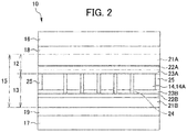
- Fig. 2 is a cross-sectional view illustrating the light control film.
- This light control film 10 is formed in a film shape for use in the laminated glass.
- the light control film 10 is bonded to, for example, a portion requiring light control.
- the usage of the light control film 10 which is bonded to the light control portion includes, for example, switching between transparent and opaque states when applied to a rear windshield of a vehicle, a glass window of a building, a showcase, an interior transparent partition, or the like.
- This light control film 10 is a light control film for controlling transmitted light using liquid crystals.
- a liquid crystal cell 15 is produced by sandwiching a liquid crystal layer 14 between a lower laminate 13 as a first laminate and an upper laminate 12 as a second laminate each having a film shape.
- the light control film 10 is produced by sandwiching the liquid crystal cell 15 between linear polarization films 16 and 17.
- a twisted nematic (TN) type is employed for driving the liquid crystal layer 14.
- various driving types such as a vertical alignment (VA) type or an in-plane switching (IPS) type may also be employed.
- VA vertical alignment
- IPS in-plane switching
- the light control film 10 has a spacer 24 provided in the upper laminate 12 and/or the lower laminate 13 to uniformly maintain a thickness of the liquid crystal layer 14.
- the linear polarization films 16 and 17 have phase difference films 18 and 19, respectively, provided on sides facing the liquid crystal cell 15 for optical compensation.
- the laminates 12 and 13 are formed by sequentially providing electrodes 22A and 22B and alignment layers 23A and 23B on bases 21A and 21B, respectively.
- the phase difference films 18 and 19 may be omitted as necessary.
- the light control film 10 may be produced by a guest-host method. In this case, a linear polarization film may be arranged on either one side or both sides of a liquid crystal cell as necessary.
- the light control film 10 is configured to be switchable between a transparent state and an opaque state by controlling transmission of external light L1 as illustrated in Figs. 3A and 3B according to a change in the voltage applied to the electrodes 22A and 22B.
- Fig. 3A illustrates a state in which no voltage is applied between the electrodes 22A and 22B
- Fig. 3B illustrates a state in which a voltage is applied to the electrodes 22A and 22B.
- the liquid crystal layer 14 is driven in a so-called normally white mode.
- the liquid crystal layer 14 may also be driven in a normally black mode.
- the electrodes 22A and 22B are produced collectively with the alignment layer 23A or 23B, and the laminates 12 and 13 are configured to match the alignment layers.
- a protection layer having a hard coat layer or the like is provided on a surface of the linear polarization film 16 and/or 17 opposite to the liquid crystal cell 15.
- the bases 21A and 21B various transparent film materials having flexibility applicable to the liquid crystal cell 15 may be applied to the bases 21A and 21B.
- a film material formed of polycarbonate and provided with hard coat layers on both sides is employed.
- Various types may be employed for the electrodes 22A and 22B as long as they can apply a substantially uniform electric field to the liquid crystal layer 14 and are visually transparent.
- the electrodes 22A and 22B are formed by producing a transparent conductive film formed of indium tin oxide (ITO) as a transparent electrode material on the entire surfaces of the bases 21A and 21B. Note that, the electrodes are patterned in desired shapes as described above in the IPS type or the like.
- ITO indium tin oxide
- the alignment layers 23A and 23B are formed from optical alignment layers.
- a variety of materials to which an optical alignment technique is applicable may be applied to this optical alignment layers.
- a photodimerization type material is employed. This photodimerization type material is disclosed in " M. Schadt, K. Schmitt, V. Kozinkov and V. Chigrinov: Jpn. J. Appl. Phys., 31, 2155 (1992 )”, “ M. Schadt, H. Seiberle and A. Schuster: Nature, 381, 212 (1996 )”, and the like.
- the alignment layers 23A and 23B may be produced through a rubbing process instead of the optical alignment layer.
- the alignment layers 23A and 23B are formed by producing various material layers applicable to the alignment layer such as polyimide and then producing a fine linear uneven shape through a rubbing process using a rubbing roll on a surface of the material layer.
- the alignment layer may be produced by producing the fine linear uneven shape through a molding process instead of the alignment layer or the optical alignment layer formed through the rubbing process.
- the spacer 24 is provided for defining a thickness of the liquid crystal layer 14, and may be formed of a variety of resin materials. According to this embodiment, the spacer 24 is produced of a photoresist. The spacer 24 is produced by coating, exposing, and developing a photoresist on the base 21B on which the transparent electrode 22B is produced. Note that the spacer 24 may be provided in the upper laminate 12 or may be provided in both the upper and lower laminates 12 and 13. Furthermore, the spacer 24 may be provided on the alignment layer 23B. Moreover, the spacer may be a so-called bead spacer.
- liquid crystal materials applicable to such a type of light control films may be applied to the liquid crystal layer 14. More specifically, a liquid crystal compound described in Japanese Unexamined Patent Application, Publication No. 2003-366484 may be applied to the liquid crystal layer 14, for example.
- a liquid crystal material, MLC2166 or the like, manufactured by Merck KGaA may be employed as a commercially available product.
- a liquid crystal material and a pigment for light control are mixed together into the liquid crystal layer 14.
- a variety of mixtures of liquid crystal material and pigment proposed in the guest-host method may be employed.
- the liquid crystal cell 15 has a seal material 25 arranged to surround the liquid crystal layer 14, so that the seal material 25 prevents leakage of the liquid crystal.
- the seal material 25 may be formed of, for example, epoxy resin, ultraviolet curable resin, or the like.
- Fig. 4 is a flowchart illustrating a producing process of the light control film 10.
- a first laminate producing process SP2 the first laminate 13 of the liquid crystal cell 15 is produced.
- the transparent electrode 22B is produced with ITO on the base 21B through sputtering or the like in an electrode producing process SP2-1.
- a coat liquid (photoresist) for the spacer 24 is coated, and the coated liquid is then subjected to drying, exposure, and development to produce the spacer 24.
- a coat liquid for the alignment layer 23B which is coated and dried is subjected to curing by irradiating ultraviolet rays, so that the alignment layer 23B is produced.
- the first laminate 13 is produced.
- the second laminate 12 is produced in a subsequent second laminate producing process SP3 similarly with the first laminate producing process SP2. That is, in the second laminate producing process SP3, the transparent electrode 22A is produced with ITO on the base 21A through sputtering or the like, and a coat liquid for the alignment layer 23A is coated, dried, and cured to produce the alignment layer 23A. As a result, the second laminate 12 is produced.
- the seal material 25 is coated in a frame shape using a dispenser. Then, a liquid crystal material is disposed in a portion of the frame shape, and the upper and lower laminates 12 and 13 are laminated and pressed. Then, the seal material 25 is cured by irradiating ultraviolet rays or the like. As a result, the liquid crystal cell 15 is produced.
- the upper and lower laminates 12 and 13 may be laminated first, and the liquid crystal material may be disposed in a cavity formed by laminating the upper and lower laminates 12 and 13.
- the light control film 10 is formed by laminating the linear polarization films 16 and 17.
- the bases 21A and 21B are provided in long films which are wound in rolls.
- the liquid crystal cell 15 undergoes all of the processes SP2 to SP5 or a part of the processes SP2 to SP5 while the bases 21A and 21B are extracted from the rolls and fed. Note that, as a result, each process for the liquid crystal cell 15 is executed piece by piece in the middle of the process as necessary.
- the spacer 24 is formed in a cylindrical rod shape or a truncated conical shape using the photoresist through the process of Fig. 4 .
- the spacer 24 is produced.
- a Vickers hardness Xs of the spacer 24 is set to 16.9 to 40.2 inclusive, and a Vickers hardness Xf of a portion of the second laminate 12 where a front end of the spacer 24 abuts is set to 11.8 to 35.9 inclusive.
- the reliability of the spacer is further increased, compared to the related art.
- the values of the Vickers hardness are measurement values under the condition described in the following Examples.
- the front end of the spacer 24 intrudes into a facing surface due to a pressing force generated during use. As a result, the cell gap may become irregular, or a local alignment failure may occur.
- the base 21A may be damaged due to a contact or like during assembly of the spacer 24, or a crack may be generated when the entire laminate is bent.
- the spacer 24 is collapsed by an external pressure, and the cell gap is reduced, so that it is difficult to obtain a desired cell gap.
- the cell gap may be reduced, or damage or a crack may be generated in some cases.
- the Vickers hardness Xs of the spacer 24 is set to 16.9 to 40.2 inclusive, and the Vickers hardness Xf of the portion of the second laminate 12 where the front end of the spacer 24 abuts is set to 11.8 to 35.9 inclusive, it is possible to simultaneously address such problems and further improve the reliability of the spacer, compared to the related art.
- Tables 1 and 2 are tables showing test results to verify the spacer.
- the tests of Examples and Comparative Examples were performed under the same condition except for the configurations of the spacer and the alignment layer where the spacer abuts. More specifically, in the light control films of Examples and Comparative Examples, the spacer 24 was provided only in the lower laminate 13, and the Vickers hardness Xs of the spacer 24 was changed by differently setting the producing condition of the spacer 24. In addition, the Vickers hardness Xf of the portion of the second laminate 12 where the front end of the spacer 24 abuts was changed by differently setting the producing condition of the alignment layer 23A.
- a coat liquid for the spacer 24 is coated and then dried. Then, a portion to be provided with the spacer 24 is selectively exposed by performing mask exposure using an exposure apparatus. Note that the above described is a positive type photoresist case. In contrast, in the case of a negative type photoresist, a portion except for the portion to be provided with the spacer 24 is selectively exposed. Then, an unexposed portion or an exposed portion of the spacer 24 is selectively removed through a developing process. Then, a rinse process or the like is executed, and a drying process or the like is executed as necessary.
- This exposure process may be performed in a so-called half cure state in which pre-heating is performed or under a heated environment in some cases.
- a heating process may be performed to promote reaction after the rinse process or the like in some cases.
- the hardness Xs of the spacer 24 is adjustable by: selecting material of the photoresist for the spacer 24; setting heating temperatures, heating times exposure amounts, exposure times and mask caps for the coating process, the exposure process and the developing process.
- lower laminates 13 having Vickers hardnesses Xs of spacers 24 each set to 14.8, 16.9, 22.2, 40.2, and 51.4 were produced by setting the heating temperatures and the heating times in the exposure process and the developing process (Table 3).
- each hardness is a measurement value measured for a lower laminate 13 which was produced by setting a producing condition of a spacer 24 and which was once assembled into a light control film 10 and separated therefrom.
- the measurement was performed by measuring twelve points in each light control film and obtaining an average of measurement values of ten points by excluding the maximum and minimum values.
- the spacer 24 was produced in a cylindrical rod shape having a diameter of 9 ⁇ m and a height of 6 ⁇ m.
- the occupation ratio increases, a stress applied to each spacer is reduced. Therefore, it is possible to reduce a collapse of the spacer 24 or intrusion of the front end.
- transmittance or a light blinding ratio may decrease accordingly.
- the occupation ratio is desirably set to 0.5% to 10% inclusive.
- alignment layers 23A of upper laminates 12 which are surfaces where the spacers abut were produced by coating a coat liquid, and drying and thermally curing the coated liquid.
- the Vickers hardnesses Xf were controlled by setting thermal curing conditions (heating temperatures and heating times) or the like.
- the upper laminates 12 having the Vickers hardnesses Xf of 10.2, 11.8, 24.8, 35.9, and 38.5 were produced (Table 4) in Examples and Comparative Examples.
- the hardness Xf is a measurement value measured for an upper laminate 12 which was once assembled into a light control film 10 and then separated therefrom.
- the upper laminates 12 were produced in advance such that the upper laminates 12 differed from each other in hardnesses of the alignment layers 23A, which are the surfaces where the spacers abut, by setting producing conditions of the alignment layers 23A. In addition, this measurement was performed by measuring twelve points and obtaining an average of ten points by excluding the maximum and minimum values.
- the Vickers hardnesses Xs and Xf were measured using PICODENTOR HM500, manufactured by Helmut Fischer GmbH. The measurement was performed by setting an insertion rate to 300 mN/20 sec, a release rate to 300 mN/20 sec, a creep time to 5 sec, and a maximum load to 100 mN.
- the microscopic observation was performed using a scanning electron microscope (SEM) or the like in front view, perspective view, and cross-sectional view to visually verify deformation of the spacer.
- SEM scanning electron microscope
- Fig. 5 is a cross-sectional view illustrating a laminated glass according to a second embodiment of the invention.
- a laminated glass 101 is similar to the laminated glass 1 of the first embodiment except for a bead spacer 124. Accordingly, like reference numerals denote like elements, and they will not be described repeatedly.
- the bead spacer 124 is provided to define a thickness of a liquid crystal layer 14.
- the bead spacer 124 can be formed using a variety of configurations such as a configuration using an inorganic material such as silica, a configuration using an organic material, and a core-shell structure using a combination of organic and inorganic materials.
- the bead spacer 124 may be formed in a rod shape such as a cylindrical rod shape and a polygonal rod shape as well as a spherical shape.
- the bead spacer 124 may be provided in an upper laminate 12 or may be provided in both upper and lower laminates 12 and 13.
- the bead spacer 124 may be provided on an alignment layer 23B.
- the bead spacer 124 is formed of a transparent material, a coloring material may be applied as necessary to control colorization.
- the second embodiment is different from the first embodiment in that the spacer producing process SP2-2 of the first embodiment is replaced with a spacer arrangement process SP2-2 in the second embodiment in which bead spacers 124 are arranged.
- a variety of arrangement methods in addition to wet/dry spraying may be applied to the bead spacers 124.
- a coat liquid obtained by dispersing the bead spacers 124 in a solvent along with a resin component is partially coated, and drying and sintering processes are sequentially executed, so that the bead spacers 124 are randomly arranged on an electrode 22B and are maintained in an immovable state. As a result, the bead spacers 124 are arranged.
- a light control film is produced by arranging the bead spacer 124 in the spacer arrangement process SP2-2, so that the Vickers hardness B of a portion of the upper laminate 12 where the bead spacer 124 abuts is set to 11.8 to 35.9 inclusive, and a product A ⁇ B is set to 0.42 or greater, where A is an occupation ratio of the bead spacer 124.
- the occupation ratio A is a ratio of an area occupied by the bead spacers 124 to an area of the lower laminate 13 when the lower laminate 13 is seen in plan view (as seen from a vertical direction).
- the Vickers hardness is a measurement value under the condition described in the following Examples and Comparative Examples.
- the Vickers hardness B of the portion of the second laminate 12 where a front end of the bead spacer 124 abuts is lower than 11.8, the front end of the bead spacer 124 intrudes into a facing surface due to a pressing force during use. As a result, a cell gap becomes irregular, or a local alignment failure occurs. In addition, in a case where the Vickers hardness B of this portion is higher than 35.9, a crack is generated when the entire laminate is bent.
- the front end of the bead spacer 124 intrudes into the facing surface. As a result, the cell gap becomes irregular, or a local alignment failure occurs.
- the Vickers hardness B of the portion of the upper laminate 12 where the bead spacer 124 abuts is set to 11.8 to 35.9 inclusive, it is possible to prevent the front end of the bead spacer 124 from intruding into the facing surface due to a pressing force during use and prevent an occurrence of a crack.
- the product A ⁇ B of the occupation ratio A and the Vickers hardness B is set to 0.42 or greater, it is possible to further reduce the intrusion of the bead spacer or a crack that may be generated by bending the laminate.
- the corresponding portion is soft. As a result, the intrusion of the bead spacer may easily occur. In contrast, in a case where the Vickers hardness B is high, the corresponding portion is stiff. Accordingly, a crack may easily occur when the corresponding portion is bent. As a result, by setting the hardness B to 11.8 to 35.9 inclusive, it is possible to reduce the intrusion of the bead spacer or the occurrence of a crack that may be generated by bending the laminate.
- Tables 5 and 6 are tables showing test results to verify bead spacers. Examples and Comparative Examples of Tables 5 and 6 were performed under the same condition except for configurations of bead spacers and alignment layers where the bead spacers abut. More specifically, in the light control films of these Examples and Comparative Examples, bead spacers 124 were provided only in lower laminates 13, and occupation ratios A were changed depending on sizes of the bead spacers 124 and application amounts of the bead spacers 124. In addition, the Vickers hardness B of the portion of a second laminate 12 where the front end of a bead spacer 124 abuts was set depending on the producing condition of an alignment layer 23A.
- a coat liquid obtained by dispersing the bead spacers 124 in a solvent along with a resin component is coated, and a drying process and a curing process by irradiating ultraviolet rays and sintering process are sequentially executed, so that the bead spacers 124 are randomly arranged on an electrode 22B and are maintained in an immovable state.
- the occupation ratio of the bead spacer 124 was controlled by adjusting an adding amount of bead spacers 124 to the coat liquid and a coating thickness of the coat liquid.
- a density of the bead spacers 124 was set to 40 pieces/mm 2 , 50 pieces/mm 2 , or 100 pieces/mm 2 , and a bead spacer 124 had a spherical shape having a diameter of 3 ⁇ m or 6 ⁇ m.
- the lower laminate 13 was produced by setting the occupation ratio A to 0.028%, 0.035%, 0.071%, 0.113%, or 0.141%.
- the bead spacer 124 was produced using the Micropearl EX series, manufactured by SEKISUI CHEMICAL CO., LTD.
- a base 21B is a cycloolefin polymer (COP) film having a hard coat layer with a thickness of 100 ⁇ m.
- the electrode 22B was produced with a thickness of 20 nm.
- An alignment layer 23B was produced by coating a coat liquid such that a coating thickness in a dried state was 100 nm and further performing thermal curing.
- the Vickers hardness B of an alignment layer 23A of the upper laminate 12 which was a surface where the bead spacer 124 abuts was controlled by setting a thermal curing condition (heating temperature and heating time) for the coated liquid which had undergone coating and drying.
- a thermal curing condition heating temperature and heating time
- upper laminates 12 having the Vickers hardnesses B of 10.2, 11.8, 35.9, and 38.5 were produced (Table 7).
- each hardness B is a measurement value measured for each of the upper laminates 12 having different hardnesses relative to the alignment layers 23A, each upper laminate 12 having been produced by setting a producing condition of the alignment layer 23A and having been once assembled into the light control film 110 and separated therefrom.
- this measurement was performed by measuring twelve points and obtaining an average of the measurement values of ten points by excluding the maximum and minimum values.
- the Vickers hardness B was measured using PICODENTOR HM500, manufactured by Helmut Fischer GmbH. The measurement was performed by setting an insertion rate to 300 mN/20 sec, a release rate to 300 mN/20 sec, a creep time to 5 sec, and a maximum load to 100 mN.
- a base 21A and an electrode 22A of the upper laminate 12 were configured similarly to the base 21B and the electrode 22B of the lower laminate 13.
- the alignment layer 23A was configured similarly to the alignment layer 23B except that the hardness B was adjusted.
- Example 1 Example 2
- Example 3 Example 4
- Example 5 Example 6
- Occupation ratio A (%) 0.035 0.035 0.071 0.141 0.141 0.113 Vickers hardness B 11.8 35.9 11.8 11.8 35.9 11.8 A ⁇ B 0.42 1.27 0.83 1.67 5.08 1.33 Film intrusion ⁇ ⁇ ⁇ ⁇ ⁇ ⁇ Crack ⁇ ⁇ ⁇ ⁇ ⁇ ⁇ [Table 7] Producing condition of alignment layer B Heating temperature of thermal curing (°C) Heating time of thermal curing (minutes) 10.2 110 30 11.8 120 10 35.9 130 30 38.5 130 60
Landscapes
- Physics & Mathematics (AREA)
- Nonlinear Science (AREA)
- Engineering & Computer Science (AREA)
- Structural Engineering (AREA)
- Civil Engineering (AREA)
- Crystallography & Structural Chemistry (AREA)
- Optics & Photonics (AREA)
- General Physics & Mathematics (AREA)
- Chemical & Material Sciences (AREA)
- Mathematical Physics (AREA)
- Architecture (AREA)
- Liquid Crystal (AREA)
- Spectroscopy & Molecular Physics (AREA)
Abstract
Description
- The present invention relates to a light control film bonded to, for example, a window and usable in an electronic window blind or the like to control transmission of external light, and a laminated glass using this light control film.
- In the related art, various techniques have been proposed for a light control film bonded to, for example, a window and usable in an electronic window blind to control transmission of external light (see
Patent Documents 1 and 2). One type of such light control films uses liquid crystals. This type of light control film using liquid crystals is produced by sandwiching a liquid crystal cell between linear polarization films. The liquid crystal cell is produced by sandwiching a liquid crystal material between transparent panels provided with transparent electrodes. As a result, the light control film controls alignment of liquid crystals to shield or transmit external light, and even to change an amount of transmitted light by changing an electric field applied to the liquid crystals and, so that the light control film controls transmission of external light. - In such a light control film, a spacer is provided on a transparent substrate of the liquid crystal cell, so that a thickness of a liquid crystal layer is uniformly maintained by this spacer. In addition, the spacer has a configuration widely used in image display panels. For example, the spacer is produced in a rod shape, for example, using a photoresist.
- In addition, a bead spacer may be employed, for example.
Patent Documents - However, in some of the light control films of the related art, the spacer may collapse or a front end of the spacer may intrude into a facing surface due to a pressing force or the like during use. As a result, in the light control films of the related art, a cell gap has become irregular, or a local alignment failure has occurred. Accordingly, there have been some cases in which it is difficult to uniformly control light and other cases in which a liquid crystal material of the liquid crystal layer leaks. As a result, the light control films of the related art have encompassed drawbacks related to practical usage of the spacer from the viewpoint of reliability.
- It may be conceived that such drawbacks may be addressed by a solution to increase the thickness of the spacer or the number of spacers. However, the solution described above may result in a decrease in transmittance or a deterioration in alignment of liquid crystals. In addition, it may be disadvantageous that diffraction light caused by the spacer may be visually recognizable.
-
- Patent Document 1: Japanese Unexamined Patent Application, Publication No.
H03-47392 - Patent Document 2: Japanese Unexamined Patent Application, Publication No.
H08-184273 - Patent Document 3: Japanese Unexamined Patent Application, Publication No.
S62-286023 - Patent Document 4: Japanese Unexamined Patent Application, Publication No.
H02-120719 - In view of such circumstances, an object of the present invention is to make it possible to further improve reliability of the spacer, compared to the related art. Means for Solving the Problems
- The inventors have made diligent studies in order to address the aforementioned problems and finally have completed the invention by achieving an idea that the reliability of the spacer is improved by selecting a Vickers hardness Xs of the spacer and a Vickers hardness Xf of a surface where a front end of the spacer abuts.
- In addition, the inventors have made diligent studies in order to address the aforementioned problems, and finally have completed the invention by achieving an idea that reliability of the spacer is improved by selecting a product A × B, where A is representative of an occupation ratio as a ratio of an area occupied by the bead spacer as seen in plan view and B is representative of a Vickers hardness of a surface where a bead spacer abuts.
- More specifically, the present invention provides the following technologies.
-
- (1) A light control film including: a first laminate having at least an alignment layer; a second laminate having at least an alignment layer; a liquid crystal layer sandwiched between the first and second laminates; and electrodes, which are provided in the first and second laminates, configured to control alignment of liquid crystal molecules of the liquid crystal layer to control transmitted light when the electrodes are driven. The first laminate has a spacer provided in a base formed of a transparent film material to maintain a thickness of the liquid crystal layer. A Vickers hardness Xs of the spacer is set to 16.9 to 40.2 inclusive, and a Vickers hardness Xf of a portion of the second laminate where a front end of the spacer abuts is set to 11.8 to 35.9 inclusive.
- According to technology (1), since the Vickers hardness Xs of the spacer is set to 16.9 to 40.2 inclusive, and the Vickers hardness Xf of the portion of the second laminate where the front end of the spacer abuts is set to 11.8 to 35.9 inclusive, it is possible to reduce intrusion of the front end of the spacer into the facing surface due to a pressing force during use or the like, reduce irregularity of cell gaps or occurrence of a local alignment failure, and effectively avoid leakage of a liquid crystal material. In addition, it is possible to reduce damage to the base and occurrence of a crack that may be generated when the entire laminate is bent. As a result, it is possible to further improve the reliability of the spacer, compared to the related art.
-
- (2) A light control film including: a first laminate having at least an alignment layer; a second laminates having at least an alignment layer; a liquid crystal layer sandwiched between the first and second laminates; and electrodes, which are provided in the first and second laminates, configured to control alignment of liquid crystal molecules of the liquid crystal layer to control transmitted light when the electrodes are driven. The first laminate has a bead spacer provided in a base formed of a transparent film material to maintain a thickness of the liquid crystal layer. A Vickers hardness B of a portion of the second laminate where the bead spacer abuts is set to 11.8 to 35.9 inclusive. A product A × B is set to 0.42 or greater, where A is an occupation ratio as a ratio of an area of the bead spacer on the first laminate when the first laminate is seen in plan view.
- According to technology (2), the Vickers hardness B is set to 11.8 to 35.9 inclusive, it is possible to reduce intrusion of the spacer into the facing surface due to a pressing force during use or the like, reduce irregularity of cell gaps or occurrence of a local alignment failure, and effectively avoid leakage of a liquid crystal material. In addition, it is possible to reduce damage to the base and occurrence of a crack that may be generated when the entire laminate is bent. Furthermore, since the product A × B of the occupation ratio A and the Vickers hardness B is set to 0.42 or greater, it is possible to increase the Vickers hardness B so as to maintain the cell gap through using the hardness B depending on a stress concentration to the bead spacer in a case where the occupation ratio A is small. Therefore, it is possible to further improve the reliability of the bead spacer, compared to the related art.
-
- (3) A laminated glass is provided which includes the light control film according to technology (1) or (2) sandwiched between plate glasses.
- According to technology (3), it is possible to configure the laminated glass using the light control film capable of further improving the reliability of the spacer, compared to the related art.
-
- (4) A method of producing a light control film, the method including: a first laminate producing process for producing a first laminate having at least an alignment layer; a second laminate producing process for producing a second laminate having at least an alignment layer; and a liquid crystal cell producing process for producing a liquid crystal cell formed by laminating the first laminate, a liquid crystal layer, and the second laminate. The first laminate producing process has a spacer producing process for producing a spacer configured to maintain a thickness of the liquid crystal layer in a base. In the spacer producing process, the spacer is produced such that a Vickers hardness Xs of the spacer becomes 16.9 to 40.2 inclusive. In the second laminate producing process, the second laminate is produced such that a Vickers hardness Xf of a portion of the second laminate where a front end of the spacer abuts becomes 11.8 to 35.9 inclusive.
- According to technology (4), since the Vickers hardness Xs of the spacer is set to 16.9 to 40.2 inclusive, and the Vickers hardness Xf of the second laminate where the front end of the spacer abuts is set to 11.8 to 35.9 inclusive, it is possible to reduce intrusion of the front end of the spacer into the facing surface due to a pressing force during use or the like, reduce irregularity of cell gaps or occurrence of a local alignment failure, and effectively avoid leakage of a liquid crystal material. In addition, it is possible to reduce damage to the base and occurrence of a crack that may be generated when the entire laminate is bent. As a result, it is possible to further improve the reliability of the spacer, compared to the related art.
-
- (5) A method of producing a light control film, the method including: a first laminate producing process for producing a first laminate having at least an alignment layer; a second laminate producing process for producing a second laminate having at least an alignment layer; and a liquid crystal cell producing process for producing a liquid crystal cell formed by laminating the first laminate, a liquid crystal layer, and the second laminate. The first laminate producing process has a bead spacer arrangement process for arranging a bead spacer configured to maintain a thickness of the liquid crystal layer in a base. In the second laminate producing process, the second laminate is produced such that a Vickers hardness B of a portion of the second laminate where the bead spacer abuts becomes 11.8 to 35.9 inclusive. In the bead spacer arrangement process, the bead spacer is arranged such that a product A × B is set to 0.42 or greater, where A is an occupation ratio as a ratio of an area of the bead spacer on the first laminate when the first laminate is seen in plan view.
- According to technology (5), since the Vickers hardness B is set to 11.8 to 35.9 inclusive, it is possible to reduce intrusion of the bead spacer into the facing surface due to a pressing force during use or the like, reduce irregularity of cell gaps or occurrence of a local alignment failure, and effectively avoid leakage of a liquid crystal material. In addition, since the product A × B of the occupation ratio A and the Vickers hardness B is set to 0.42 or greater, it is possible to increase the Vickers hardness B so as to maintain the cell gap through using the hardness B depending on a stress concentration to the bead spacer in a case where the occupation ratio A is small. As a result, it is possible to further reduce the intrusion of the bead spacer into the facing surface, reduce the irregularity of cell gaps or the occurrence of a local alignment failure, and effectively avoid the leakage of a liquid crystal material. Therefore, it is possible to further improve the reliability of the bead spacer, compared to the related art.
- According to the present invention, it is possible to further improve the reliability of the spacer in the light control film using liquid crystals, compared to the related art.
-
-
Fig. 1 is a diagram illustrating a laminated glass according to a first embodiment of the invention; -
Fig. 2 is a diagram illustrating a light control film used in the laminated glass ofFig. 1 ; -
Figs. 3A and 3B are diagrams describing the principle of operation for the light control film ofFig. 2 ; -
Fig. 4 is a flowchart illustrating a producing process of the light control film ofFig. 2 ; -
Fig. 5 is a diagram illustrating a laminated glass according to a second embodiment of the invention; and -
Fig. 6 is a diagram illustrating a light control film used in the laminated glass ofFig. 5 . -
Fig. 1 is a cross-sectional view illustrating a laminated glass according to a first embodiment of the invention. Alaminated glass 1 is a laminated glass applied to, for example, a vehicle window in which alight control film 10 is sandwiched betweenplate glasses middle layers plate glasses middle layers light control film 10 and theplate glass middle layers - The
plate glasses middle layers light control film 10. Subsequently, theplate glasses light control film 10 are integrated with each other via themiddle layers laminated glass 1, the entirety of which is formed in a desired curved shape, by heating and pressing. As a result, thelaminated glass 1 is produced applicable to, for example, a rear windshield of a vehicle or the like and to control transmitted light through thelight control film 10. Note that the producing process of thelaminated glass 1 includes a laminating process for laminating theplate glasses middle layers light control film 10 and a heating/pressing process for heating and pressing the laminate obtained in the laminating process. -
Fig. 2 is a cross-sectional view illustrating the light control film. Thislight control film 10 is formed in a film shape for use in the laminated glass. In another usage, thelight control film 10 is bonded to, for example, a portion requiring light control. In this connection, the usage of thelight control film 10 which is bonded to the light control portion includes, for example, switching between transparent and opaque states when applied to a rear windshield of a vehicle, a glass window of a building, a showcase, an interior transparent partition, or the like. - This
light control film 10 is a light control film for controlling transmitted light using liquid crystals. Aliquid crystal cell 15 is produced by sandwiching a liquid crystal layer 14 between alower laminate 13 as a first laminate and anupper laminate 12 as a second laminate each having a film shape. Thelight control film 10 is produced by sandwiching theliquid crystal cell 15 betweenlinear polarization films light control film 10 has aspacer 24 provided in theupper laminate 12 and/or thelower laminate 13 to uniformly maintain a thickness of the liquid crystal layer 14. Thelinear polarization films phase difference films liquid crystal cell 15 for optical compensation. Thelaminates electrodes alignment layers bases phase difference films light control film 10 may be produced by a guest-host method. In this case, a linear polarization film may be arranged on either one side or both sides of a liquid crystal cell as necessary. - As a result, the
light control film 10 is configured to be switchable between a transparent state and an opaque state by controlling transmission of external light L1 as illustrated inFigs. 3A and 3B according to a change in the voltage applied to theelectrodes Fig. 3A illustrates a state in which no voltage is applied between theelectrodes Fig. 3B illustrates a state in which a voltage is applied to theelectrodes electrodes alignment layer laminates - Incidentally, in a usage where the
light control film 10 is bonded, for example, to a glass window of a building, a showcase, an interior transparent partition, or the like, a protection layer having a hard coat layer or the like is provided on a surface of thelinear polarization film 16 and/or 17 opposite to theliquid crystal cell 15. - Here, various transparent film materials having flexibility applicable to the
liquid crystal cell 15 may be applied to thebases electrodes electrodes bases - The alignment layers 23A and 23B are formed from optical alignment layers. Here, a variety of materials to which an optical alignment technique is applicable may be applied to this optical alignment layers. However, according to this embodiment, for example, a photodimerization type material is employed. This photodimerization type material is disclosed in "M. Schadt, K. Schmitt, V. Kozinkov and V. Chigrinov: Jpn. J. Appl. Phys., 31, 2155 (1992)", "M. Schadt, H. Seiberle and A. Schuster: Nature, 381, 212 (1996)", and the like.
- Alternatively, the alignment layers 23A and 23B may be produced through a rubbing process instead of the optical alignment layer. In this case, the alignment layers 23A and 23B are formed by producing various material layers applicable to the alignment layer such as polyimide and then producing a fine linear uneven shape through a rubbing process using a rubbing roll on a surface of the material layer. Alternatively, the alignment layer may be produced by producing the fine linear uneven shape through a molding process instead of the alignment layer or the optical alignment layer formed through the rubbing process.
- The
spacer 24 is provided for defining a thickness of the liquid crystal layer 14, and may be formed of a variety of resin materials. According to this embodiment, thespacer 24 is produced of a photoresist. Thespacer 24 is produced by coating, exposing, and developing a photoresist on thebase 21B on which thetransparent electrode 22B is produced. Note that thespacer 24 may be provided in theupper laminate 12 or may be provided in both the upper andlower laminates spacer 24 may be provided on thealignment layer 23B. Moreover, the spacer may be a so-called bead spacer. - A variety of liquid crystal materials applicable to such a type of light control films may be applied to the liquid crystal layer 14. More specifically, a liquid crystal compound described in Japanese Unexamined Patent Application, Publication No.
2003-366484 liquid crystal cell 15 has aseal material 25 arranged to surround the liquid crystal layer 14, so that theseal material 25 prevents leakage of the liquid crystal. Here, theseal material 25 may be formed of, for example, epoxy resin, ultraviolet curable resin, or the like. -
Fig. 4 is a flowchart illustrating a producing process of thelight control film 10. In a first laminate producing process SP2, thefirst laminate 13 of theliquid crystal cell 15 is produced. - In the first laminate producing process SP2, the
transparent electrode 22B is produced with ITO on thebase 21B through sputtering or the like in an electrode producing process SP2-1. - In a subsequent spacer producing process SP2-2, a coat liquid (photoresist) for the
spacer 24 is coated, and the coated liquid is then subjected to drying, exposure, and development to produce thespacer 24. - Subsequently, in an alignment layer producing process SP2-3, a coat liquid for the
alignment layer 23B which is coated and dried is subjected to curing by irradiating ultraviolet rays, so that thealignment layer 23B is produced. As a result, according to this embodiment, thefirst laminate 13 is produced. - In the process of producing the
light control film 10, thesecond laminate 12 is produced in a subsequent second laminate producing process SP3 similarly with the first laminate producing process SP2. That is, in the second laminate producing process SP3, thetransparent electrode 22A is produced with ITO on thebase 21A through sputtering or the like, and a coat liquid for thealignment layer 23A is coated, dried, and cured to produce thealignment layer 23A. As a result, thesecond laminate 12 is produced. - In a subsequent liquid crystal cell producing process SP4, the
seal material 25 is coated in a frame shape using a dispenser. Then, a liquid crystal material is disposed in a portion of the frame shape, and the upper andlower laminates seal material 25 is cured by irradiating ultraviolet rays or the like. As a result, theliquid crystal cell 15 is produced. Alternatively, in the arrangement of the liquid crystal material, the upper andlower laminates lower laminates - In a subsequent laminating process SP5, the
light control film 10 is formed by laminating thelinear polarization films bases liquid crystal cell 15 undergoes all of the processes SP2 to SP5 or a part of the processes SP2 to SP5 while thebases liquid crystal cell 15 is executed piece by piece in the middle of the process as necessary. - Here, according to this embodiment, the
spacer 24 is formed in a cylindrical rod shape or a truncated conical shape using the photoresist through the process ofFig. 4 . As a result, thespacer 24 is produced. According to this embodiment, a Vickers hardness Xs of thespacer 24 is set to 16.9 to 40.2 inclusive, and a Vickers hardness Xf of a portion of thesecond laminate 12 where a front end of thespacer 24 abuts is set to 11.8 to 35.9 inclusive. As a result, the reliability of the spacer is further increased, compared to the related art. Note that the values of the Vickers hardness are measurement values under the condition described in the following Examples. - That is, in a case where the Vickers hardness Xf of the portion of the
second laminate 12 where the front end of thespacer 24 abuts is lower than 11.8, the front end of thespacer 24 intrudes into a facing surface due to a pressing force generated during use. As a result, the cell gap may become irregular, or a local alignment failure may occur. In addition, in this case, thebase 21A may be damaged due to a contact or like during assembly of thespacer 24, or a crack may be generated when the entire laminate is bent. - In addition, in a case where the Vickers hardness Xs of the
spacer 24 is lower than 16.9, thespacer 24 is collapsed by an external pressure, and the cell gap is reduced, so that it is difficult to obtain a desired cell gap. In addition, in a case where the Vickers hardness Xs of thespacer 24 is higher than 40.2, or in a case where the Vickers hardness Xf of the portion of thesecond laminate 12 where the front end of thespacer 24 abuts is higher than 35.9, the cell gap may be reduced, or damage or a crack may be generated in some cases. - However, in a case where the Vickers hardness Xs of the
spacer 24 is set to 16.9 to 40.2 inclusive, and the Vickers hardness Xf of the portion of thesecond laminate 12 where the front end of thespacer 24 abuts is set to 11.8 to 35.9 inclusive, it is possible to simultaneously address such problems and further improve the reliability of the spacer, compared to the related art. - Tables 1 and 2 are tables showing test results to verify the spacer. In Tables 1 and 2, the tests of Examples and Comparative Examples were performed under the same condition except for the configurations of the spacer and the alignment layer where the spacer abuts. More specifically, in the light control films of Examples and Comparative Examples, the
spacer 24 was provided only in thelower laminate 13, and the Vickers hardness Xs of thespacer 24 was changed by differently setting the producing condition of thespacer 24. In addition, the Vickers hardness Xf of the portion of thesecond laminate 12 where the front end of thespacer 24 abuts was changed by differently setting the producing condition of thealignment layer 23A. - That is, a coat liquid for the
spacer 24 is coated and then dried. Then, a portion to be provided with thespacer 24 is selectively exposed by performing mask exposure using an exposure apparatus. Note that the above described is a positive type photoresist case. In contrast, in the case of a negative type photoresist, a portion except for the portion to be provided with thespacer 24 is selectively exposed. Then, an unexposed portion or an exposed portion of thespacer 24 is selectively removed through a developing process. Then, a rinse process or the like is executed, and a drying process or the like is executed as necessary. - This exposure process may be performed in a so-called half cure state in which pre-heating is performed or under a heated environment in some cases. In addition, in the developing process, a heating process may be performed to promote reaction after the rinse process or the like in some cases. The hardness Xs of the
spacer 24 is adjustable by: selecting material of the photoresist for thespacer 24; setting heating temperatures, heating times exposure amounts, exposure times and mask caps for the coating process, the exposure process and the developing process. - According to this embodiment,
lower laminates 13 having Vickers hardnesses Xs ofspacers 24 each set to 14.8, 16.9, 22.2, 40.2, and 51.4 were produced by setting the heating temperatures and the heating times in the exposure process and the developing process (Table 3). Note that each hardness is a measurement value measured for alower laminate 13 which was produced by setting a producing condition of aspacer 24 and which was once assembled into alight control film 10 and separated therefrom. In addition, the measurement was performed by measuring twelve points in each light control film and obtaining an average of measurement values of ten points by excluding the maximum and minimum values. - Incidentally, the
spacer 24 was produced in a cylindrical rod shape having a diameter of 9 µm and a height of 6 µm. In addition, thespacers 24 were arranged with a pitch of 110 µm along two directions perpendicular to each other in a plane of thebase 21B. Therefore, a ratio of an area occupied by aspacer 24 on thebase 21B (occupation ratio) was set to 0.5% (= ((9/2)2 × 3) / (110)2). - As the occupation ratio increases, a stress applied to each spacer is reduced. Therefore, it is possible to reduce a collapse of the
spacer 24 or intrusion of the front end. However, transmittance or a light blinding ratio may decrease accordingly. To the contrary, in a case where the occupation ratio is small, it may be possible to ensure an optical property such as transmittance and a light blinding ratio. However, it may be difficult to avoid a phenomenon such as a collapse of thespacer 24 or intrusion of the front end. As a result, the occupation ratio is desirably set to 0.5% to 10% inclusive. - In comparison, alignment layers 23A of
upper laminates 12 which are surfaces where the spacers abut were produced by coating a coat liquid, and drying and thermally curing the coated liquid. The Vickers hardnesses Xf were controlled by setting thermal curing conditions (heating temperatures and heating times) or the like. As a result, theupper laminates 12 having the Vickers hardnesses Xf of 10.2, 11.8, 24.8, 35.9, and 38.5 were produced (Table 4) in Examples and Comparative Examples. Note that the hardness Xf is a measurement value measured for anupper laminate 12 which was once assembled into alight control film 10 and then separated therefrom. Theupper laminates 12 were produced in advance such that theupper laminates 12 differed from each other in hardnesses of the alignment layers 23A, which are the surfaces where the spacers abut, by setting producing conditions of the alignment layers 23A. In addition, this measurement was performed by measuring twelve points and obtaining an average of ten points by excluding the maximum and minimum values. - Incidentally, the Vickers hardnesses Xs and Xf were measured using PICODENTOR HM500, manufactured by Helmut Fischer GmbH. The measurement was performed by setting an insertion rate to 300 mN/20 sec, a release rate to 300 mN/20 sec, a creep time to 5 sec, and a maximum load to 100 mN.
- In Examples and Comparative Examples of Tables 1 and 2, light control films were produced and tested using the upper and
lower laminates - Here, the microscopic observation was performed using a scanning electron microscope (SEM) or the like in front view, perspective view, and cross-sectional view to visually verify deformation of the spacer. In a case where deformation of the spacer was verified, it was determined whether the deformation is "reduction of cell gap or collapse of spacer" depending on its situation, and ○/X marks were added to the tables. Accordingly, in Tables 1 and 2, the mark "○" indicates a normal case where no anomalousness was observed for the corresponding item, and the mark "X" indicates an abnormal case where anomalousness was observed for the corresponding item.
- In addition, similarly, the portion where the spacer abuts was observed using a SEM or the like in perspective view. In this case, when a hollow (recess) was verified, the item "film intrusion" was determined as "X". When the recess was not verified, the item "film intrusion" was determined as "○".
- In addition, an occurrence of damage was visually verified by displacing relative positions of the
laminates laminates - In addition, an occurrence of a crack was verified by winding the light control film around a cylindrical mandrel having a diameter of 2 mm in accordance with a bending test regulation of the JIS K5600-5-1. In a case where the occurrence of a crack in the base was verified for a half or more of the plurality of samples, in this test, the item "crack (film)" is marked as "X". In contrast, in a case where the occurrence of a crack in the base was not verified for a half or more of the plurality of samples, the item "crack" is marked as "X".


[Table 3] Producing condition of spacer Xs Photoresist material Heating temperature in coating process (°C) Heating time in coating process (minutes) Light exposure (mJ) Exposure time (seconds) 14.8 Acrylic positive-type photoresist 130 30 80 20 16.9 130 60 90 23 22.2 130 60 100 25 40.2 140 60 150 38 51.4 140 120 150 38 [Table 4] Producing condition of alignment layer Xf Heating temperature of thermal curing (°C) Heating time of thermal curing (minutes) 10.2 110 30 11.8 120 10 24.8 120 30 35.9 130 30 38.5 130 60 - In the measurement results of Tables 1 and 2, in a case where the Vickers hardness Xs of the
spacer 24 was lower than 16.9 (Comparative Examples 5 and 7), reduction of the cell gap was verified. In addition, in Comparative Example 5, intrusion of the front end of the spacer into the film, damage, and cracks were verified. Furthermore, in a case where the Vickers hardness Xf of the portion of thesecond laminate 12 where the front end of thespacer 24 abuts was lower than 11.8 (Comparative Examples 1 and 3), damage and cracks were observed. Moreover, in Comparative Example 3, intrusion of the front end of the spacer to the film was observed. - In addition, in a case where the Vickers hardness Xs of the
spacer 24 was higher than 40.2 (Comparative Examples 6 and 8), reduction of the cell gap and intrusion of the front end of the spacer into the film were observed in Comparative Example 6, and damage was observed in Comparative Example 8. In addition, in a case where the Vickers hardness Xf of the portion of thesecond laminate 12 where the front end of thespacer 24 abuts was higher than 35.9 (Comparative Examples 2 and 4), reduction of the cell gap and damage were observed. Furthermore, in Comparative Example 4, a crack was observed. - To the contrary, in Examples 1 to 13, such phenomena were not observed. As a result, it was demonstrated that the reliability of the spacer is sufficiently achievable.
-
Fig. 5 is a cross-sectional view illustrating a laminated glass according to a second embodiment of the invention. Alaminated glass 101 is similar to thelaminated glass 1 of the first embodiment except for abead spacer 124. Accordingly, like reference numerals denote like elements, and they will not be described repeatedly. - The
bead spacer 124 is provided to define a thickness of a liquid crystal layer 14. Thebead spacer 124 can be formed using a variety of configurations such as a configuration using an inorganic material such as silica, a configuration using an organic material, and a core-shell structure using a combination of organic and inorganic materials. In addition, thebead spacer 124 may be formed in a rod shape such as a cylindrical rod shape and a polygonal rod shape as well as a spherical shape. Thebead spacer 124 may be provided in anupper laminate 12 or may be provided in both upper andlower laminates bead spacer 124 may be provided on analignment layer 23B. Furthermore, while thebead spacer 124 is formed of a transparent material, a coloring material may be applied as necessary to control colorization. - Since the process of producing a
light control film 110 is similar to the process ofFig. 4 of the first embodiment, the process will not be described repeatedly. The second embodiment is different from the first embodiment in that the spacer producing process SP2-2 of the first embodiment is replaced with a spacer arrangement process SP2-2 in the second embodiment in whichbead spacers 124 are arranged. - Here, a variety of arrangement methods in addition to wet/dry spraying may be applied to the
bead spacers 124. According to this embodiment, a coat liquid obtained by dispersing thebead spacers 124 in a solvent along with a resin component is partially coated, and drying and sintering processes are sequentially executed, so that thebead spacers 124 are randomly arranged on anelectrode 22B and are maintained in an immovable state. As a result, thebead spacers 124 are arranged. - Here, according to this embodiment, a light control film is produced by arranging the
bead spacer 124 in the spacer arrangement process SP2-2, so that the Vickers hardness B of a portion of theupper laminate 12 where thebead spacer 124 abuts is set to 11.8 to 35.9 inclusive, and a product A × B is set to 0.42 or greater, where A is an occupation ratio of thebead spacer 124. Note that, here, the occupation ratio A is a ratio of an area occupied by thebead spacers 124 to an area of thelower laminate 13 when thelower laminate 13 is seen in plan view (as seen from a vertical direction). As a result, according to this embodiment, it is possible to further improve the reliability of the bead spacer, compared to the related art. Note that the Vickers hardness is a measurement value under the condition described in the following Examples and Comparative Examples. - In a case where the Vickers hardness B of the portion of the
second laminate 12 where a front end of thebead spacer 124 abuts is lower than 11.8, the front end of thebead spacer 124 intrudes into a facing surface due to a pressing force during use. As a result, a cell gap becomes irregular, or a local alignment failure occurs. In addition, in a case where the Vickers hardness B of this portion is higher than 35.9, a crack is generated when the entire laminate is bent. - In addition, in a case where the product A × B is lower than 0.42, the front end of the
bead spacer 124 intrudes into the facing surface. As a result, the cell gap becomes irregular, or a local alignment failure occurs. - However, it is possible to simultaneously address such problems and further improve the reliability of the bead spacer compared to the related art by setting the Vickers hardness B of the portion of the
upper laminate 12 where thebead spacer 124 abuts to 11.8 to 35.9 inclusive and setting the product A × B to 0.42 or greater. - Specifically, in a case where the Vickers hardness B of the portion of the
upper laminate 12 where thebead spacer 124 abuts is set to 11.8 to 35.9 inclusive, it is possible to prevent the front end of thebead spacer 124 from intruding into the facing surface due to a pressing force during use and prevent an occurrence of a crack. In addition, in a case where the product A × B of the occupation ratio A and the Vickers hardness B is set to 0.42 or greater, it is possible to further reduce the intrusion of the bead spacer or a crack that may be generated by bending the laminate. - That is, in a case where the Vickers hardness B is low, it can be said that the corresponding portion is soft. As a result, the intrusion of the bead spacer may easily occur. In contrast, in a case where the Vickers hardness B is high, the corresponding portion is stiff. Accordingly, a crack may easily occur when the corresponding portion is bent. As a result, by setting the hardness B to 11.8 to 35.9 inclusive, it is possible to reduce the intrusion of the bead spacer or the occurrence of a crack that may be generated by bending the laminate.
- However, even when the hardness B is set in this manner, a magnitude of the stress applied to one spacer changes depending on the number of spacers. In a case where the occupation ratio A, which is an index of the magnitude, is low, a stress concentration on one spacer increases. As a result, in a case where the product A × B is smaller than 0.42 even when the hardness B is set to 11.8 to 35.9 inclusive, the bead spacer may easily intrude. In addition, in a case where the occupation ratio A is low, a stress concentration relating to bending increases due to the small number of spacers. As a result, in a case where the product A × B is smaller than 0.42 even when the hardness B is set to 11.8 to 35.9 inclusive, a crack may easily occur. For these reasons, it is possible to further improve the reliability of the bead spacer, compared to the related art, by not only setting the Vickers hardness B to 11.8 to 35.9 inclusive but also setting the product A × B to 0.42 or greater.
- Tables 5 and 6 are tables showing test results to verify bead spacers. Examples and Comparative Examples of Tables 5 and 6 were performed under the same condition except for configurations of bead spacers and alignment layers where the bead spacers abut. More specifically, in the light control films of these Examples and Comparative Examples,
bead spacers 124 were provided only inlower laminates 13, and occupation ratios A were changed depending on sizes of thebead spacers 124 and application amounts of thebead spacers 124. In addition, the Vickers hardness B of the portion of asecond laminate 12 where the front end of abead spacer 124 abuts was set depending on the producing condition of analignment layer 23A. - That is, a coat liquid obtained by dispersing the
bead spacers 124 in a solvent along with a resin component is coated, and a drying process and a curing process by irradiating ultraviolet rays and sintering process are sequentially executed, so that thebead spacers 124 are randomly arranged on anelectrode 22B and are maintained in an immovable state. The occupation ratio of thebead spacer 124 was controlled by adjusting an adding amount ofbead spacers 124 to the coat liquid and a coating thickness of the coat liquid. - In Examples and Comparative Examples, a density of the
bead spacers 124 was set to 40 pieces/mm2, 50 pieces/mm2, or 100 pieces/mm2, and abead spacer 124 had a spherical shape having a diameter of 3 µm or 6 µm. As a result, thelower laminate 13 was produced by setting the occupation ratio A to 0.028%, 0.035%, 0.071%, 0.113%, or 0.141%. Note that thebead spacer 124 was produced using the Micropearl EX series, manufactured by SEKISUI CHEMICAL CO., LTD. - A
base 21B is a cycloolefin polymer (COP) film having a hard coat layer with a thickness of 100 µm. Theelectrode 22B was produced with a thickness of 20 nm. - An
alignment layer 23B was produced by coating a coat liquid such that a coating thickness in a dried state was 100 nm and further performing thermal curing. - In comparison, similar to the
alignment layer 23B, the Vickers hardness B of analignment layer 23A of theupper laminate 12 which was a surface where thebead spacer 124 abuts was controlled by setting a thermal curing condition (heating temperature and heating time) for the coated liquid which had undergone coating and drying. As a result, in Examples and Comparative Examples,upper laminates 12 having the Vickers hardnesses B of 10.2, 11.8, 35.9, and 38.5 were produced (Table 7). Note that each hardness B is a measurement value measured for each of theupper laminates 12 having different hardnesses relative to the alignment layers 23A, eachupper laminate 12 having been produced by setting a producing condition of thealignment layer 23A and having been once assembled into thelight control film 110 and separated therefrom. In addition, this measurement was performed by measuring twelve points and obtaining an average of the measurement values of ten points by excluding the maximum and minimum values. - Incidentally, the Vickers hardness B was measured using PICODENTOR HM500, manufactured by Helmut Fischer GmbH. The measurement was performed by setting an insertion rate to 300 mN/20 sec, a release rate to 300 mN/20 sec, a creep time to 5 sec, and a maximum load to 100 mN.
- Incidentally, a
base 21A and anelectrode 22A of theupper laminate 12 were configured similarly to thebase 21B and theelectrode 22B of thelower laminate 13. Note that thealignment layer 23A was configured similarly to thealignment layer 23B except that the hardness B was adjusted. - In Examples and Comparative Examples of Tables 5 and 6, light control films were produced and tested using upper and
lower laminates - Here, in a case where a hollow (recess) was verified by observing the portion where the
bead spacer 124 abuts using a SEM or the like in perspective view, the item "film intrusion" was marked as "X". In a case where no recess was verified, the item "film intrusion" was marked as "○". - In addition, an occurrence of a crack was verified by winding a light control film around a cylindrical mandrel having a diameter of 2 mm in accordance with a bending test regulation of JIS K5600-5-1. In a case where the occurrence of a crack in the base was verified for a half or more of a plurality of samples, in this test, the item "crack" was marked as "X". In contrast, in a case where the occurrence of a crack in the base was not verified for a half or more of the plurality of samples, the item "crack" was marked as "○".
[Table 5] Example 1 Example 2 Example 3 Example 4 Example 5 Example 6 Bead diameter (µm) 3 3 3 6 6 6 Density (Pieces/mm2) 50 50 100 50 50 40 Occupation ratio A (%) 0.035 0.035 0.071 0.141 0.141 0.113 Vickers hardness B 11.8 35.9 11.8 11.8 35.9 11.8 A×B 0.42 1.27 0.83 1.67 5.08 1.33 Film intrusion ○ ○ ○ ○ ○ ○ Crack ○ ○ ○ ○ ○ ○ 

[Table 7] Producing condition of alignment layer B Heating temperature of thermal curing (°C) Heating time of thermal curing (minutes) 10.2 110 30 11.8 120 10 35.9 130 30 38.5 130 60 - In the measurement results of Tables 5 and 6, it was verified that the film intrusion was prevented, and no crack was generated in a case where the Vickers hardness B of the portion of the
second laminate 12 where thebead spacer 124 abuts was set to 11.8 to 35.9 inclusive, and the product A × B was set to 0.42 or greater, where A representative of the occupation ratio and B representative of the Vickers hardness. As a result, it was demonstrated that the reliability of the bead spacer was sufficiently achievable. - While preferable embodiments of the present invention have been described in detail hereinbefore, various modifications or alterations of the above embodiments may be possible without departing from the spirit and scope of the invention.
-
- 1, 101
- LAMINATED GLASS
- 2, 3
- PLATE GLASS
- 4, 5
- MIDDLE LAYER
- 10, 110
- LIGHT CONTROL FILM
- 12
- UPPER LAMINATE
- 13
- LOWER LAMINATE
- 14
- LIQUID CRYSTAL LAYER
- 14A
- LIQUID CRYSTAL MOLECULES
- 15
- LIQUID CRYSTAL CELL
- 16, 17
- LINEAR POLARIZATION FILM
- 18, 19
- PHASE DIFFERENCE FILM
- 21A, 21B
- BASE
- 22A, 22B
- ELECTRODE
- 23A, 23B
- ALIGNMENT LAYER
- 24
- SPACER
- 25
- SEAL MATERIAL
- 124
- BEAD SPACER
Claims (5)
- A light control film comprising:a first laminate having at least an alignment layer;a second laminate having at least an alignment layer;a liquid crystal layer sandwiched between the first and second laminates; andelectrodes, which are provided in the first and second laminates, configured to control alignment of liquid crystal molecules of the liquid crystal layer to control transmitted light when the electrodes are driven,wherein the first laminate has a spacer provided in a base formed of a transparent film material to maintain a thickness of the liquid crystal layer, and
a Vickers hardness Xs of the spacer is set to 16.9 to 40.2 inclusive, and a Vickers hardness Xf of a portion of the second laminate where a front end of the spacer abuts is set to 11.8 to 35.9 inclusive. - A light control film comprising:a first laminate having at least an alignment layer;a second laminate having at least an alignment layer;a liquid crystal layer sandwiched between the first and second laminates; andelectrodes, which are provided in the first and second laminates, configured to control alignment of liquid crystal molecules of the liquid crystal layer to control transmitted light when the electrodes are driven,wherein the first laminate has a bead spacer provided in a base formed of a transparent film material to maintain a thickness of the liquid crystal layer, and
wherein a Vickers hardness B of a portion of the second laminate where the bead spacer abuts is set to 11.8 to 35.9 inclusive, and
a product A × B is set to 0.42 or greater, where A is an occupation ratio representative of a ratio of an area of the bead spacer on the first laminate when the first laminate is seen in plan view. - A laminated glass comprising the light control film according to claim 1 or 2 sandwiched between plate glasses.
- A method of producing a light control film, the method comprising:a first laminate producing process for producing a first laminate having at least an alignment layer;a second laminate producing process for producing a second laminate having at least an alignment layer; anda liquid crystal cell producing process for producing a liquid crystal cell formed by laminating the first laminate, a liquid crystal layer, and the second laminate,wherein the first laminate producing process has a spacer producing process for producing a spacer configured to maintain a thickness of the liquid crystal layer in a base,
wherein in the spacer producing process, the spacer is produced such that a Vickers hardness Xs of the spacer becomes 16.9 to 40.2 inclusive,
wherein in the second laminate producing process, the second laminate is produced such that a Vickers hardness Xf of a portion of the second laminate where a front end of the spacer abuts becomes 11.8 to 35.9 inclusive. - A method of producing a light control film, the method comprising:a first laminate producing process for producing a first laminate having at least an alignment layer;a second laminate producing process for producing a second laminate having at least an alignment layer; anda liquid crystal cell producing process for producing a liquid crystal cell formed by laminating the first laminate, a liquid crystal layer, and the second laminate,wherein the first laminate producing process has a bead spacer arrangement process for arranging a bead spacer configured to maintain a thickness of the liquid crystal layer in a base,
wherein in the second laminate producing process, the second laminate is produced such that a Vickers hardness B of a portion of the second laminate where the bead spacer abuts becomes 11.8 to 35.9 inclusive, and
wherein in the bead spacer arrangement process, the bead spacer is arranged such that a product A × B is set to 0.42 or greater, where A is an occupation ratio representative of a ratio of an area of the bead spacer on the first laminate when the first laminate is seen in plan view.
Applications Claiming Priority (3)
| Application Number | Priority Date | Filing Date | Title |
|---|---|---|---|
| JP2016085392A JP6065142B1 (en) | 2016-04-21 | 2016-04-21 | Light control film, laminated glass, and method for manufacturing light control film |
| JP2016087131A JP6065143B1 (en) | 2016-04-25 | 2016-04-25 | Light control film, laminated glass, and method for manufacturing light control film |
| PCT/JP2017/015895 WO2017183692A1 (en) | 2016-04-21 | 2017-04-20 | Light control film, laminated glass and method for producing light control film |
Publications (3)
| Publication Number | Publication Date |
|---|---|
| EP3447566A1 true EP3447566A1 (en) | 2019-02-27 |
| EP3447566A4 EP3447566A4 (en) | 2019-10-02 |
| EP3447566B1 EP3447566B1 (en) | 2020-05-27 |
Family
ID=60116186
Family Applications (1)
| Application Number | Title | Priority Date | Filing Date |
|---|---|---|---|
| EP17786029.3A Not-in-force EP3447566B1 (en) | 2016-04-21 | 2017-04-20 | Light control film, laminated glass and method for producing light control film |
Country Status (5)
| Country | Link |
|---|---|
| US (2) | US10732464B2 (en) |
| EP (1) | EP3447566B1 (en) |
| KR (1) | KR102226630B1 (en) |
| CN (1) | CN109073923B (en) |
| WO (1) | WO2017183692A1 (en) |
Families Citing this family (24)
| Publication number | Priority date | Publication date | Assignee | Title |
|---|---|---|---|---|
| US10670911B2 (en) * | 2016-05-20 | 2020-06-02 | Sharp Kabushiki Kaisha | Liquid crystal display panel and liquid crystal display device |
| WO2018195458A1 (en) | 2017-04-20 | 2018-10-25 | Cardinal Ig Company | High performance privacy glazing structures |
| WO2019014613A1 (en) | 2017-07-13 | 2019-01-17 | Cardinal Ig Company | Electrical connection configurations for privacy glazing structures |
| KR102607588B1 (en) * | 2017-11-02 | 2023-11-30 | 다이니폰 인사츠 가부시키가이샤 | Manufacturing method of laminated glass, laminated glass, dimming film |
| WO2019090341A1 (en) | 2017-11-06 | 2019-05-09 | Cardinal Ig Company | Privacy glazing system with discrete electrical driver |
| JP7440266B2 (en) * | 2017-11-24 | 2024-02-28 | 大日本印刷株式会社 | Laminated glass, liquid crystal film |
| JP6414312B1 (en) * | 2017-11-27 | 2018-10-31 | 凸版印刷株式会社 | Light control unit and window light control plate |
| US11644717B2 (en) | 2018-01-17 | 2023-05-09 | Sekisui Chemical Co., Ltd. | Dimming laminate and resin spacer for dimming laminate |
| KR102939378B1 (en) | 2018-03-27 | 2026-03-13 | 세키스이가가쿠 고교가부시키가이샤 | Light dimmer and light-dimmer window glass |
| MX2020011871A (en) | 2018-05-09 | 2021-01-20 | Cardinal Ig Co | Electrically controllable privacy glazing with energy recapturing driver. |
| WO2020037185A1 (en) | 2018-08-17 | 2020-02-20 | Cardinal Ig Company | Privacy glazing structure with asymetrical pane offsets for electrical connection configurations |
| US11474385B1 (en) | 2018-12-02 | 2022-10-18 | Cardinal Ig Company | Electrically controllable privacy glazing with ultralow power consumption comprising a liquid crystal material having a light transmittance that varies in response to application of an electric field |
| WO2020163836A1 (en) | 2019-02-08 | 2020-08-13 | Cardinal Ig Company | Low power driver for privacy glazing |
| WO2020223277A1 (en) | 2019-04-29 | 2020-11-05 | Cardinal Ig Company | Staggered driving electrical control of a plurality of electrically controllable privacy glazing structures |
| MX2021013262A (en) | 2019-04-29 | 2022-01-06 | Cardinal Ig Co | DETECTION AND CONTROL OF LEAKAGE CURRENT FOR ONE OR MORE GLAZING STRUCTURES WITH ELECTRICALLY CONTROLLABLE PRIVACY. |
| US11448910B2 (en) | 2019-04-29 | 2022-09-20 | Cardinal Ig Company | Systems and methods for operating one or more electrically controllable privacy glazing structures |
| CN111624800A (en) * | 2020-06-29 | 2020-09-04 | 京东方科技集团股份有限公司 | Dimming structure and manufacturing method thereof, and dimming module |
| US20250020959A1 (en) * | 2021-11-24 | 2025-01-16 | Corning Incorporated | Liquid crystal devices resistant to gravity mura and related methods |
| US12130521B1 (en) | 2021-12-16 | 2024-10-29 | Apple Inc. | Windows with liquid crystal layers |
| KR102909396B1 (en) | 2022-03-17 | 2026-01-08 | 동우 화인켐 주식회사 | Optical laminate, and manufacturing method for the same, and smart window including the same |
| KR102681560B1 (en) | 2022-03-24 | 2024-07-04 | 동우 화인켐 주식회사 | Transmittance variable optical laminate and manufacturing method for the same, and smart window including the same |
| KR20230166461A (en) | 2022-05-31 | 2023-12-07 | 동우 화인켐 주식회사 | Transmittance variable optical laminate and manufacturing method for the same, and smart window including the same |
| KR102628860B1 (en) * | 2022-06-07 | 2024-01-25 | 동우 화인켐 주식회사 | Optical laminate, and manufacturing method for the same, and smart window including the same |
| KR20240106181A (en) | 2022-12-29 | 2024-07-08 | 동우 화인켐 주식회사 | Optical laminate, and manufacturing method for the same, and smart window comprising the same |
Family Cites Families (27)
| Publication number | Priority date | Publication date | Assignee | Title |
|---|---|---|---|---|
| JPS62286023A (en) | 1986-06-04 | 1987-12-11 | Toyota Motor Corp | Production of liquid crystal cell |
| JP2527467B2 (en) | 1988-10-29 | 1996-08-21 | シャープ株式会社 | Liquid crystal display manufacturing method |
| JPH0347392A (en) | 1989-07-12 | 1991-02-28 | Natl House Ind Co Ltd | liquid crystal panel |
| JP3158667B2 (en) * | 1991-08-01 | 2001-04-23 | セイコーエプソン株式会社 | Method of manufacturing liquid crystal display element and method of reproducing liquid crystal display element |
| JPH0817288A (en) * | 1994-07-04 | 1996-01-19 | Matsushita Electric Ind Co Ltd | Transparent touch panel |
| JPH08184273A (en) | 1994-12-27 | 1996-07-16 | Ohbayashi Corp | Lighting control glass window |
| JP3299869B2 (en) * | 1995-09-27 | 2002-07-08 | シャープ株式会社 | Liquid crystal display device and manufacturing method thereof |
| JPH112821A (en) * | 1997-06-13 | 1999-01-06 | Sony Corp | Liquid crystal element and manufacturing method thereof |
| JPH112820A (en) * | 1997-06-13 | 1999-01-06 | Sharp Corp | Liquid crystal display |
| US7411211B1 (en) * | 1999-07-22 | 2008-08-12 | Semiconductor Energy Laboratory Co., Ltd. | Contact structure and semiconductor device |
| JP2001083525A (en) | 1999-09-09 | 2001-03-30 | Canon Inc | Color filter with spacer, method of manufacturing the same, and liquid crystal element using the color filter |
| JP2001100188A (en) * | 1999-09-30 | 2001-04-13 | Ricoh Co Ltd | Liquid crystal display element |
| US6812977B1 (en) * | 1999-11-22 | 2004-11-02 | Minolta Co., Ltd. | Liquid crystal element |
| JP2001174619A (en) | 1999-12-14 | 2001-06-29 | Shin Sti Technology Kk | Color filter for liquid crystal |
| JP3890841B2 (en) | 1999-12-24 | 2007-03-07 | 旭硝子株式会社 | LCD light control window for vehicles |
| JP2002198374A (en) * | 2000-10-16 | 2002-07-12 | Sharp Corp | Semiconductor device and method of manufacturing the same |
| JP4024516B2 (en) * | 2001-10-18 | 2007-12-19 | シャープ株式会社 | Liquid crystal display |
| JP2004069749A (en) * | 2002-08-01 | 2004-03-04 | Casio Comput Co Ltd | Liquid crystal display device |
| JP4929578B2 (en) * | 2003-11-10 | 2012-05-09 | 大日本印刷株式会社 | Liquid crystal display |
| KR101114233B1 (en) * | 2005-04-29 | 2012-03-06 | 엘지디스플레이 주식회사 | Liquid Crystal Display Panel and Method for Fabricating Thereof |
| JP4901198B2 (en) * | 2005-11-28 | 2012-03-21 | 大日本印刷株式会社 | Substrate for display device with spacer |
| JP4774954B2 (en) * | 2005-11-28 | 2011-09-21 | 大日本印刷株式会社 | Substrate for display device with spacer |
| KR101296653B1 (en) | 2007-10-05 | 2013-08-14 | 엘지디스플레이 주식회사 | Liquid crystal Display Device and Method for Manufacturing the Same |
| AU2010214431B2 (en) * | 2009-02-13 | 2014-05-29 | Hitachi Chemical Company, Ltd. | Light modulation film |
| JP2012203184A (en) * | 2011-03-25 | 2012-10-22 | Toppan Printing Co Ltd | Color filter substrate and liquid crystal display device having the same |
| CN104714338A (en) * | 2013-12-16 | 2015-06-17 | 群创光电股份有限公司 | Liquid crystal display panel |
| JP6413320B2 (en) * | 2014-04-28 | 2018-10-31 | 凸版印刷株式会社 | Column spacer for color filter for liquid crystal display device, color filter for liquid crystal display device, and liquid crystal display device |
-
2017
- 2017-04-20 CN CN201780024336.3A patent/CN109073923B/en active Active
- 2017-04-20 EP EP17786029.3A patent/EP3447566B1/en not_active Not-in-force
- 2017-04-20 WO PCT/JP2017/015895 patent/WO2017183692A1/en not_active Ceased
- 2017-04-20 KR KR1020187031683A patent/KR102226630B1/en active Active
- 2017-04-20 US US16/094,330 patent/US10732464B2/en active Active
-
2020
- 2020-06-26 US US16/913,293 patent/US11150521B2/en active Active
Also Published As
| Publication number | Publication date |
|---|---|
| US20190121186A1 (en) | 2019-04-25 |
| EP3447566B1 (en) | 2020-05-27 |
| US10732464B2 (en) | 2020-08-04 |
| WO2017183692A1 (en) | 2017-10-26 |
| EP3447566A4 (en) | 2019-10-02 |
| CN109073923B (en) | 2021-11-26 |
| CN109073923A (en) | 2018-12-21 |
| KR102226630B1 (en) | 2021-03-12 |
| KR20180132782A (en) | 2018-12-12 |
| US11150521B2 (en) | 2021-10-19 |
| US20200326577A1 (en) | 2020-10-15 |
Similar Documents
| Publication | Publication Date | Title |
|---|---|---|
| US11150521B2 (en) | Light control film, laminated glass and method for producing light control film | |
| JP7435667B2 (en) | Light control film and laminated glass | |
| JP5910788B1 (en) | Light control film, laminated glass, and method for manufacturing light control film | |
| US20110051066A1 (en) | Apparatus and method of fabricating alignment layer for liquid crystal display | |
| JP6065142B1 (en) | Light control film, laminated glass, and method for manufacturing light control film | |
| JP6665661B2 (en) | Light control film, method for manufacturing light control film | |
| JP6065143B1 (en) | Light control film, laminated glass, and method for manufacturing light control film | |
| EP4386475A2 (en) | Light control film and laminated glass | |
| JP6065144B1 (en) | Light control film | |
| JP6183492B1 (en) | Light control film and method of manufacturing light control film | |
| JP6048606B1 (en) | Light control film and method of manufacturing light control film | |
| JP6103108B1 (en) | Light control film and method of manufacturing light control film | |
| JP2017198731A (en) | Lighting control film and manufacturing method of lighting control film | |
| WO2017170578A1 (en) | Light-controlling film and method for manufacturing light-controlling film | |
| JP2018049232A (en) | Liquid crystal cell |
Legal Events
| Date | Code | Title | Description |
|---|---|---|---|
| STAA | Information on the status of an ep patent application or granted ep patent |
Free format text: STATUS: THE INTERNATIONAL PUBLICATION HAS BEEN MADE |
|
| PUAI | Public reference made under article 153(3) epc to a published international application that has entered the european phase |
Free format text: ORIGINAL CODE: 0009012 |
|
| STAA | Information on the status of an ep patent application or granted ep patent |
Free format text: STATUS: REQUEST FOR EXAMINATION WAS MADE |
|
| 17P | Request for examination filed |
Effective date: 20181115 |
|
| AK | Designated contracting states |
Kind code of ref document: A1 Designated state(s): AL AT BE BG CH CY CZ DE DK EE ES FI FR GB GR HR HU IE IS IT LI LT LU LV MC MK MT NL NO PL PT RO RS SE SI SK SM TR |
|
| AX | Request for extension of the european patent |
Extension state: BA ME |
|
| DAV | Request for validation of the european patent (deleted) | ||
| DAX | Request for extension of the european patent (deleted) | ||
| A4 | Supplementary search report drawn up and despatched |
Effective date: 20190830 |
|
| RIC1 | Information provided on ipc code assigned before grant |
Ipc: G02F 1/1339 20060101ALI20190826BHEP Ipc: E06B 9/24 20060101ALI20190826BHEP Ipc: E06B 3/66 20060101AFI20190826BHEP |
|
| REG | Reference to a national code |
Ref country code: DE Ref legal event code: R079 Ref document number: 602017017438 Country of ref document: DE Free format text: PREVIOUS MAIN CLASS: G02F0001130000 Ipc: E06B0003660000 |
|
| RIC1 | Information provided on ipc code assigned before grant |
Ipc: E06B 9/24 20060101ALI20191114BHEP Ipc: E06B 3/66 20060101AFI20191114BHEP Ipc: G02F 1/1339 20060101ALI20191114BHEP |
|
| GRAP | Despatch of communication of intention to grant a patent |
Free format text: ORIGINAL CODE: EPIDOSNIGR1 |
|
| STAA | Information on the status of an ep patent application or granted ep patent |
Free format text: STATUS: GRANT OF PATENT IS INTENDED |
|
| INTG | Intention to grant announced |
Effective date: 20200108 |
|
| GRAS | Grant fee paid |
Free format text: ORIGINAL CODE: EPIDOSNIGR3 |
|
| GRAA | (expected) grant |
Free format text: ORIGINAL CODE: 0009210 |
|
| STAA | Information on the status of an ep patent application or granted ep patent |
Free format text: STATUS: THE PATENT HAS BEEN GRANTED |
|
| AK | Designated contracting states |
Kind code of ref document: B1 Designated state(s): AL AT BE BG CH CY CZ DE DK EE ES FI FR GB GR HR HU IE IS IT LI LT LU LV MC MK MT NL NO PL PT RO RS SE SI SK SM TR |
|
| REG | Reference to a national code |
Ref country code: GB Ref legal event code: FG4D |
|
| REG | Reference to a national code |
Ref country code: CH Ref legal event code: EP |
|
| REG | Reference to a national code |
Ref country code: AT Ref legal event code: REF Ref document number: 1274723 Country of ref document: AT Kind code of ref document: T Effective date: 20200615 |
|
| REG | Reference to a national code |
Ref country code: DE Ref legal event code: R096 Ref document number: 602017017438 Country of ref document: DE |
|
| REG | Reference to a national code |
Ref country code: LT Ref legal event code: MG4D |
|
| PG25 | Lapsed in a contracting state [announced via postgrant information from national office to epo] |
Ref country code: FI Free format text: LAPSE BECAUSE OF FAILURE TO SUBMIT A TRANSLATION OF THE DESCRIPTION OR TO PAY THE FEE WITHIN THE PRESCRIBED TIME-LIMIT Effective date: 20200527 Ref country code: NO Free format text: LAPSE BECAUSE OF FAILURE TO SUBMIT A TRANSLATION OF THE DESCRIPTION OR TO PAY THE FEE WITHIN THE PRESCRIBED TIME-LIMIT Effective date: 20200827 Ref country code: GR Free format text: LAPSE BECAUSE OF FAILURE TO SUBMIT A TRANSLATION OF THE DESCRIPTION OR TO PAY THE FEE WITHIN THE PRESCRIBED TIME-LIMIT Effective date: 20200828 Ref country code: PT Free format text: LAPSE BECAUSE OF FAILURE TO SUBMIT A TRANSLATION OF THE DESCRIPTION OR TO PAY THE FEE WITHIN THE PRESCRIBED TIME-LIMIT Effective date: 20200928 Ref country code: SE Free format text: LAPSE BECAUSE OF FAILURE TO SUBMIT A TRANSLATION OF THE DESCRIPTION OR TO PAY THE FEE WITHIN THE PRESCRIBED TIME-LIMIT Effective date: 20200527 Ref country code: IS Free format text: LAPSE BECAUSE OF FAILURE TO SUBMIT A TRANSLATION OF THE DESCRIPTION OR TO PAY THE FEE WITHIN THE PRESCRIBED TIME-LIMIT Effective date: 20200927 Ref country code: LT Free format text: LAPSE BECAUSE OF FAILURE TO SUBMIT A TRANSLATION OF THE DESCRIPTION OR TO PAY THE FEE WITHIN THE PRESCRIBED TIME-LIMIT Effective date: 20200527 |
|
| REG | Reference to a national code |
Ref country code: NL Ref legal event code: MP Effective date: 20200527 |
|
| PG25 | Lapsed in a contracting state [announced via postgrant information from national office to epo] |
Ref country code: BG Free format text: LAPSE BECAUSE OF FAILURE TO SUBMIT A TRANSLATION OF THE DESCRIPTION OR TO PAY THE FEE WITHIN THE PRESCRIBED TIME-LIMIT Effective date: 20200827 Ref country code: HR Free format text: LAPSE BECAUSE OF FAILURE TO SUBMIT A TRANSLATION OF THE DESCRIPTION OR TO PAY THE FEE WITHIN THE PRESCRIBED TIME-LIMIT Effective date: 20200527 Ref country code: LV Free format text: LAPSE BECAUSE OF FAILURE TO SUBMIT A TRANSLATION OF THE DESCRIPTION OR TO PAY THE FEE WITHIN THE PRESCRIBED TIME-LIMIT Effective date: 20200527 Ref country code: RS Free format text: LAPSE BECAUSE OF FAILURE TO SUBMIT A TRANSLATION OF THE DESCRIPTION OR TO PAY THE FEE WITHIN THE PRESCRIBED TIME-LIMIT Effective date: 20200527 |
|
| REG | Reference to a national code |
Ref country code: AT Ref legal event code: MK05 Ref document number: 1274723 Country of ref document: AT Kind code of ref document: T Effective date: 20200527 |
|
| PG25 | Lapsed in a contracting state [announced via postgrant information from national office to epo] |
Ref country code: NL Free format text: LAPSE BECAUSE OF FAILURE TO SUBMIT A TRANSLATION OF THE DESCRIPTION OR TO PAY THE FEE WITHIN THE PRESCRIBED TIME-LIMIT Effective date: 20200527 Ref country code: AL Free format text: LAPSE BECAUSE OF FAILURE TO SUBMIT A TRANSLATION OF THE DESCRIPTION OR TO PAY THE FEE WITHIN THE PRESCRIBED TIME-LIMIT Effective date: 20200527 |
|
| PG25 | Lapsed in a contracting state [announced via postgrant information from national office to epo] |
Ref country code: ES Free format text: LAPSE BECAUSE OF FAILURE TO SUBMIT A TRANSLATION OF THE DESCRIPTION OR TO PAY THE FEE WITHIN THE PRESCRIBED TIME-LIMIT Effective date: 20200527 Ref country code: AT Free format text: LAPSE BECAUSE OF FAILURE TO SUBMIT A TRANSLATION OF THE DESCRIPTION OR TO PAY THE FEE WITHIN THE PRESCRIBED TIME-LIMIT Effective date: 20200527 Ref country code: DK Free format text: LAPSE BECAUSE OF FAILURE TO SUBMIT A TRANSLATION OF THE DESCRIPTION OR TO PAY THE FEE WITHIN THE PRESCRIBED TIME-LIMIT Effective date: 20200527 Ref country code: SM Free format text: LAPSE BECAUSE OF FAILURE TO SUBMIT A TRANSLATION OF THE DESCRIPTION OR TO PAY THE FEE WITHIN THE PRESCRIBED TIME-LIMIT Effective date: 20200527 Ref country code: EE Free format text: LAPSE BECAUSE OF FAILURE TO SUBMIT A TRANSLATION OF THE DESCRIPTION OR TO PAY THE FEE WITHIN THE PRESCRIBED TIME-LIMIT Effective date: 20200527 Ref country code: CZ Free format text: LAPSE BECAUSE OF FAILURE TO SUBMIT A TRANSLATION OF THE DESCRIPTION OR TO PAY THE FEE WITHIN THE PRESCRIBED TIME-LIMIT Effective date: 20200527 Ref country code: RO Free format text: LAPSE BECAUSE OF FAILURE TO SUBMIT A TRANSLATION OF THE DESCRIPTION OR TO PAY THE FEE WITHIN THE PRESCRIBED TIME-LIMIT Effective date: 20200527 |
|
| PG25 | Lapsed in a contracting state [announced via postgrant information from national office to epo] |
Ref country code: PL Free format text: LAPSE BECAUSE OF FAILURE TO SUBMIT A TRANSLATION OF THE DESCRIPTION OR TO PAY THE FEE WITHIN THE PRESCRIBED TIME-LIMIT Effective date: 20200527 Ref country code: SK Free format text: LAPSE BECAUSE OF FAILURE TO SUBMIT A TRANSLATION OF THE DESCRIPTION OR TO PAY THE FEE WITHIN THE PRESCRIBED TIME-LIMIT Effective date: 20200527 |
|
| REG | Reference to a national code |
Ref country code: DE Ref legal event code: R097 Ref document number: 602017017438 Country of ref document: DE |
|
| PLBE | No opposition filed within time limit |
Free format text: ORIGINAL CODE: 0009261 |
|
| STAA | Information on the status of an ep patent application or granted ep patent |
Free format text: STATUS: NO OPPOSITION FILED WITHIN TIME LIMIT |
|
| 26N | No opposition filed |
Effective date: 20210302 |
|
| PG25 | Lapsed in a contracting state [announced via postgrant information from national office to epo] |
Ref country code: SI Free format text: LAPSE BECAUSE OF FAILURE TO SUBMIT A TRANSLATION OF THE DESCRIPTION OR TO PAY THE FEE WITHIN THE PRESCRIBED TIME-LIMIT Effective date: 20200527 |
|
| PGFP | Annual fee paid to national office [announced via postgrant information from national office to epo] |
Ref country code: DE Payment date: 20210420 Year of fee payment: 5 Ref country code: IT Payment date: 20210427 Year of fee payment: 5 Ref country code: FR Payment date: 20210423 Year of fee payment: 5 |
|
| PGFP | Annual fee paid to national office [announced via postgrant information from national office to epo] |
Ref country code: GB Payment date: 20210422 Year of fee payment: 5 |
|
| PG25 | Lapsed in a contracting state [announced via postgrant information from national office to epo] |
Ref country code: MC Free format text: LAPSE BECAUSE OF FAILURE TO SUBMIT A TRANSLATION OF THE DESCRIPTION OR TO PAY THE FEE WITHIN THE PRESCRIBED TIME-LIMIT Effective date: 20200527 |
|
| PG25 | Lapsed in a contracting state [announced via postgrant information from national office to epo] |
Ref country code: LU Free format text: LAPSE BECAUSE OF NON-PAYMENT OF DUE FEES Effective date: 20210420 |
|
| REG | Reference to a national code |
Ref country code: BE Ref legal event code: MM Effective date: 20210430 |
|
| PG25 | Lapsed in a contracting state [announced via postgrant information from national office to epo] |
Ref country code: CH Free format text: LAPSE BECAUSE OF NON-PAYMENT OF DUE FEES Effective date: 20210430 Ref country code: LI Free format text: LAPSE BECAUSE OF NON-PAYMENT OF DUE FEES Effective date: 20210430 |
|
| PG25 | Lapsed in a contracting state [announced via postgrant information from national office to epo] |
Ref country code: IE Free format text: LAPSE BECAUSE OF NON-PAYMENT OF DUE FEES Effective date: 20210420 |
|
| PG25 | Lapsed in a contracting state [announced via postgrant information from national office to epo] |
Ref country code: BE Free format text: LAPSE BECAUSE OF NON-PAYMENT OF DUE FEES Effective date: 20210430 |
|
| REG | Reference to a national code |
Ref country code: DE Ref legal event code: R119 Ref document number: 602017017438 Country of ref document: DE |
|
| GBPC | Gb: european patent ceased through non-payment of renewal fee |
Effective date: 20220420 |
|
| PG25 | Lapsed in a contracting state [announced via postgrant information from national office to epo] |
Ref country code: GB Free format text: LAPSE BECAUSE OF NON-PAYMENT OF DUE FEES Effective date: 20220420 Ref country code: FR Free format text: LAPSE BECAUSE OF NON-PAYMENT OF DUE FEES Effective date: 20220430 Ref country code: DE Free format text: LAPSE BECAUSE OF NON-PAYMENT OF DUE FEES Effective date: 20221103 |
|
| PG25 | Lapsed in a contracting state [announced via postgrant information from national office to epo] |
Ref country code: IT Free format text: LAPSE BECAUSE OF NON-PAYMENT OF DUE FEES Effective date: 20220420 |
|
| PG25 | Lapsed in a contracting state [announced via postgrant information from national office to epo] |
Ref country code: CY Free format text: LAPSE BECAUSE OF FAILURE TO SUBMIT A TRANSLATION OF THE DESCRIPTION OR TO PAY THE FEE WITHIN THE PRESCRIBED TIME-LIMIT Effective date: 20200527 |
|
| PG25 | Lapsed in a contracting state [announced via postgrant information from national office to epo] |
Ref country code: HU Free format text: LAPSE BECAUSE OF FAILURE TO SUBMIT A TRANSLATION OF THE DESCRIPTION OR TO PAY THE FEE WITHIN THE PRESCRIBED TIME-LIMIT; INVALID AB INITIO Effective date: 20170420 |
|
| PG25 | Lapsed in a contracting state [announced via postgrant information from national office to epo] |
Ref country code: MK Free format text: LAPSE BECAUSE OF FAILURE TO SUBMIT A TRANSLATION OF THE DESCRIPTION OR TO PAY THE FEE WITHIN THE PRESCRIBED TIME-LIMIT Effective date: 20200527 |
|
| PG25 | Lapsed in a contracting state [announced via postgrant information from national office to epo] |
Ref country code: MT Free format text: LAPSE BECAUSE OF FAILURE TO SUBMIT A TRANSLATION OF THE DESCRIPTION OR TO PAY THE FEE WITHIN THE PRESCRIBED TIME-LIMIT Effective date: 20200527 |
|
| PG25 | Lapsed in a contracting state [announced via postgrant information from national office to epo] |
Ref country code: TR Free format text: LAPSE BECAUSE OF FAILURE TO SUBMIT A TRANSLATION OF THE DESCRIPTION OR TO PAY THE FEE WITHIN THE PRESCRIBED TIME-LIMIT Effective date: 20200527 |