EP3446814A1 - Surface-coated cutting tool - Google Patents
Surface-coated cutting tool Download PDFInfo
- Publication number
- EP3446814A1 EP3446814A1 EP17785670.5A EP17785670A EP3446814A1 EP 3446814 A1 EP3446814 A1 EP 3446814A1 EP 17785670 A EP17785670 A EP 17785670A EP 3446814 A1 EP3446814 A1 EP 3446814A1
- Authority
- EP
- European Patent Office
- Prior art keywords
- layer
- composition
- substrate
- coating film
- alternate
- Prior art date
- Legal status (The legal status is an assumption and is not a legal conclusion. Google has not performed a legal analysis and makes no representation as to the accuracy of the status listed.)
- Granted
Links
Images


Classifications
-
- C—CHEMISTRY; METALLURGY
- C23—COATING METALLIC MATERIAL; COATING MATERIAL WITH METALLIC MATERIAL; CHEMICAL SURFACE TREATMENT; DIFFUSION TREATMENT OF METALLIC MATERIAL; COATING BY VACUUM EVAPORATION, BY SPUTTERING, BY ION IMPLANTATION OR BY CHEMICAL VAPOUR DEPOSITION, IN GENERAL; INHIBITING CORROSION OF METALLIC MATERIAL OR INCRUSTATION IN GENERAL
- C23C—COATING METALLIC MATERIAL; COATING MATERIAL WITH METALLIC MATERIAL; SURFACE TREATMENT OF METALLIC MATERIAL BY DIFFUSION INTO THE SURFACE, BY CHEMICAL CONVERSION OR SUBSTITUTION; COATING BY VACUUM EVAPORATION, BY SPUTTERING, BY ION IMPLANTATION OR BY CHEMICAL VAPOUR DEPOSITION, IN GENERAL
- C23C28/00—Coating for obtaining at least two superposed coatings either by methods not provided for in a single one of groups C23C2/00 - C23C26/00 or by combinations of methods provided for in subclasses C23C and C25C or C25D
- C23C28/40—Coatings including alternating layers following a pattern, a periodic or defined repetition
- C23C28/42—Coatings including alternating layers following a pattern, a periodic or defined repetition characterized by the composition of the alternating layers
-
- B—PERFORMING OPERATIONS; TRANSPORTING
- B23—MACHINE TOOLS; METAL-WORKING NOT OTHERWISE PROVIDED FOR
- B23B—TURNING; BORING
- B23B27/00—Tools for turning or boring machines; Tools of a similar kind in general; Accessories therefor
- B23B27/14—Cutting tools of which the bits or tips or cutting inserts are of special material
- B23B27/148—Composition of the cutting inserts
-
- B—PERFORMING OPERATIONS; TRANSPORTING
- B23—MACHINE TOOLS; METAL-WORKING NOT OTHERWISE PROVIDED FOR
- B23B—TURNING; BORING
- B23B27/00—Tools for turning or boring machines; Tools of a similar kind in general; Accessories therefor
- B23B27/14—Cutting tools of which the bits or tips or cutting inserts are of special material
-
- C—CHEMISTRY; METALLURGY
- C23—COATING METALLIC MATERIAL; COATING MATERIAL WITH METALLIC MATERIAL; CHEMICAL SURFACE TREATMENT; DIFFUSION TREATMENT OF METALLIC MATERIAL; COATING BY VACUUM EVAPORATION, BY SPUTTERING, BY ION IMPLANTATION OR BY CHEMICAL VAPOUR DEPOSITION, IN GENERAL; INHIBITING CORROSION OF METALLIC MATERIAL OR INCRUSTATION IN GENERAL
- C23C—COATING METALLIC MATERIAL; COATING MATERIAL WITH METALLIC MATERIAL; SURFACE TREATMENT OF METALLIC MATERIAL BY DIFFUSION INTO THE SURFACE, BY CHEMICAL CONVERSION OR SUBSTITUTION; COATING BY VACUUM EVAPORATION, BY SPUTTERING, BY ION IMPLANTATION OR BY CHEMICAL VAPOUR DEPOSITION, IN GENERAL
- C23C14/00—Coating by vacuum evaporation, by sputtering or by ion implantation of the coating forming material
- C23C14/02—Pretreatment of the material to be coated
- C23C14/021—Cleaning or etching treatments
- C23C14/022—Cleaning or etching treatments by means of bombardment with energetic particles or radiation
-
- C—CHEMISTRY; METALLURGY
- C23—COATING METALLIC MATERIAL; COATING MATERIAL WITH METALLIC MATERIAL; CHEMICAL SURFACE TREATMENT; DIFFUSION TREATMENT OF METALLIC MATERIAL; COATING BY VACUUM EVAPORATION, BY SPUTTERING, BY ION IMPLANTATION OR BY CHEMICAL VAPOUR DEPOSITION, IN GENERAL; INHIBITING CORROSION OF METALLIC MATERIAL OR INCRUSTATION IN GENERAL
- C23C—COATING METALLIC MATERIAL; COATING MATERIAL WITH METALLIC MATERIAL; SURFACE TREATMENT OF METALLIC MATERIAL BY DIFFUSION INTO THE SURFACE, BY CHEMICAL CONVERSION OR SUBSTITUTION; COATING BY VACUUM EVAPORATION, BY SPUTTERING, BY ION IMPLANTATION OR BY CHEMICAL VAPOUR DEPOSITION, IN GENERAL
- C23C14/00—Coating by vacuum evaporation, by sputtering or by ion implantation of the coating forming material
- C23C14/02—Pretreatment of the material to be coated
- C23C14/024—Deposition of sublayers, e.g. to promote adhesion of the coating
- C23C14/025—Metallic sublayers
-
- C—CHEMISTRY; METALLURGY
- C23—COATING METALLIC MATERIAL; COATING MATERIAL WITH METALLIC MATERIAL; CHEMICAL SURFACE TREATMENT; DIFFUSION TREATMENT OF METALLIC MATERIAL; COATING BY VACUUM EVAPORATION, BY SPUTTERING, BY ION IMPLANTATION OR BY CHEMICAL VAPOUR DEPOSITION, IN GENERAL; INHIBITING CORROSION OF METALLIC MATERIAL OR INCRUSTATION IN GENERAL
- C23C—COATING METALLIC MATERIAL; COATING MATERIAL WITH METALLIC MATERIAL; SURFACE TREATMENT OF METALLIC MATERIAL BY DIFFUSION INTO THE SURFACE, BY CHEMICAL CONVERSION OR SUBSTITUTION; COATING BY VACUUM EVAPORATION, BY SPUTTERING, BY ION IMPLANTATION OR BY CHEMICAL VAPOUR DEPOSITION, IN GENERAL
- C23C14/00—Coating by vacuum evaporation, by sputtering or by ion implantation of the coating forming material
- C23C14/06—Coating by vacuum evaporation, by sputtering or by ion implantation of the coating forming material characterised by the coating material
-
- C—CHEMISTRY; METALLURGY
- C23—COATING METALLIC MATERIAL; COATING MATERIAL WITH METALLIC MATERIAL; CHEMICAL SURFACE TREATMENT; DIFFUSION TREATMENT OF METALLIC MATERIAL; COATING BY VACUUM EVAPORATION, BY SPUTTERING, BY ION IMPLANTATION OR BY CHEMICAL VAPOUR DEPOSITION, IN GENERAL; INHIBITING CORROSION OF METALLIC MATERIAL OR INCRUSTATION IN GENERAL
- C23C—COATING METALLIC MATERIAL; COATING MATERIAL WITH METALLIC MATERIAL; SURFACE TREATMENT OF METALLIC MATERIAL BY DIFFUSION INTO THE SURFACE, BY CHEMICAL CONVERSION OR SUBSTITUTION; COATING BY VACUUM EVAPORATION, BY SPUTTERING, BY ION IMPLANTATION OR BY CHEMICAL VAPOUR DEPOSITION, IN GENERAL
- C23C14/00—Coating by vacuum evaporation, by sputtering or by ion implantation of the coating forming material
- C23C14/06—Coating by vacuum evaporation, by sputtering or by ion implantation of the coating forming material characterised by the coating material
- C23C14/0617—AIII BV compounds, where A is Al, Ga, In or Tl and B is N, P, As, Sb or Bi
-
- C—CHEMISTRY; METALLURGY
- C23—COATING METALLIC MATERIAL; COATING MATERIAL WITH METALLIC MATERIAL; CHEMICAL SURFACE TREATMENT; DIFFUSION TREATMENT OF METALLIC MATERIAL; COATING BY VACUUM EVAPORATION, BY SPUTTERING, BY ION IMPLANTATION OR BY CHEMICAL VAPOUR DEPOSITION, IN GENERAL; INHIBITING CORROSION OF METALLIC MATERIAL OR INCRUSTATION IN GENERAL
- C23C—COATING METALLIC MATERIAL; COATING MATERIAL WITH METALLIC MATERIAL; SURFACE TREATMENT OF METALLIC MATERIAL BY DIFFUSION INTO THE SURFACE, BY CHEMICAL CONVERSION OR SUBSTITUTION; COATING BY VACUUM EVAPORATION, BY SPUTTERING, BY ION IMPLANTATION OR BY CHEMICAL VAPOUR DEPOSITION, IN GENERAL
- C23C14/00—Coating by vacuum evaporation, by sputtering or by ion implantation of the coating forming material
- C23C14/22—Coating by vacuum evaporation, by sputtering or by ion implantation of the coating forming material characterised by the process of coating
- C23C14/24—Vacuum evaporation
- C23C14/32—Vacuum evaporation by explosion; by evaporation and subsequent ionisation of the vapours, e.g. ion-plating
- C23C14/325—Electric arc evaporation
-
- C—CHEMISTRY; METALLURGY
- C23—COATING METALLIC MATERIAL; COATING MATERIAL WITH METALLIC MATERIAL; CHEMICAL SURFACE TREATMENT; DIFFUSION TREATMENT OF METALLIC MATERIAL; COATING BY VACUUM EVAPORATION, BY SPUTTERING, BY ION IMPLANTATION OR BY CHEMICAL VAPOUR DEPOSITION, IN GENERAL; INHIBITING CORROSION OF METALLIC MATERIAL OR INCRUSTATION IN GENERAL
- C23C—COATING METALLIC MATERIAL; COATING MATERIAL WITH METALLIC MATERIAL; SURFACE TREATMENT OF METALLIC MATERIAL BY DIFFUSION INTO THE SURFACE, BY CHEMICAL CONVERSION OR SUBSTITUTION; COATING BY VACUUM EVAPORATION, BY SPUTTERING, BY ION IMPLANTATION OR BY CHEMICAL VAPOUR DEPOSITION, IN GENERAL
- C23C28/00—Coating for obtaining at least two superposed coatings either by methods not provided for in a single one of groups C23C2/00 - C23C26/00 or by combinations of methods provided for in subclasses C23C and C25C or C25D
- C23C28/04—Coating for obtaining at least two superposed coatings either by methods not provided for in a single one of groups C23C2/00 - C23C26/00 or by combinations of methods provided for in subclasses C23C and C25C or C25D only coatings of inorganic non-metallic material
- C23C28/044—Coating for obtaining at least two superposed coatings either by methods not provided for in a single one of groups C23C2/00 - C23C26/00 or by combinations of methods provided for in subclasses C23C and C25C or C25D only coatings of inorganic non-metallic material coatings specially adapted for cutting tools or wear applications
-
- C—CHEMISTRY; METALLURGY
- C23—COATING METALLIC MATERIAL; COATING MATERIAL WITH METALLIC MATERIAL; CHEMICAL SURFACE TREATMENT; DIFFUSION TREATMENT OF METALLIC MATERIAL; COATING BY VACUUM EVAPORATION, BY SPUTTERING, BY ION IMPLANTATION OR BY CHEMICAL VAPOUR DEPOSITION, IN GENERAL; INHIBITING CORROSION OF METALLIC MATERIAL OR INCRUSTATION IN GENERAL
- C23C—COATING METALLIC MATERIAL; COATING MATERIAL WITH METALLIC MATERIAL; SURFACE TREATMENT OF METALLIC MATERIAL BY DIFFUSION INTO THE SURFACE, BY CHEMICAL CONVERSION OR SUBSTITUTION; COATING BY VACUUM EVAPORATION, BY SPUTTERING, BY ION IMPLANTATION OR BY CHEMICAL VAPOUR DEPOSITION, IN GENERAL
- C23C28/00—Coating for obtaining at least two superposed coatings either by methods not provided for in a single one of groups C23C2/00 - C23C26/00 or by combinations of methods provided for in subclasses C23C and C25C or C25D
- C23C28/04—Coating for obtaining at least two superposed coatings either by methods not provided for in a single one of groups C23C2/00 - C23C26/00 or by combinations of methods provided for in subclasses C23C and C25C or C25D only coatings of inorganic non-metallic material
- C23C28/048—Coating for obtaining at least two superposed coatings either by methods not provided for in a single one of groups C23C2/00 - C23C26/00 or by combinations of methods provided for in subclasses C23C and C25C or C25D only coatings of inorganic non-metallic material with layers graded in composition or physical properties
-
- C—CHEMISTRY; METALLURGY
- C23—COATING METALLIC MATERIAL; COATING MATERIAL WITH METALLIC MATERIAL; CHEMICAL SURFACE TREATMENT; DIFFUSION TREATMENT OF METALLIC MATERIAL; COATING BY VACUUM EVAPORATION, BY SPUTTERING, BY ION IMPLANTATION OR BY CHEMICAL VAPOUR DEPOSITION, IN GENERAL; INHIBITING CORROSION OF METALLIC MATERIAL OR INCRUSTATION IN GENERAL
- C23C—COATING METALLIC MATERIAL; COATING MATERIAL WITH METALLIC MATERIAL; SURFACE TREATMENT OF METALLIC MATERIAL BY DIFFUSION INTO THE SURFACE, BY CHEMICAL CONVERSION OR SUBSTITUTION; COATING BY VACUUM EVAPORATION, BY SPUTTERING, BY ION IMPLANTATION OR BY CHEMICAL VAPOUR DEPOSITION, IN GENERAL
- C23C28/00—Coating for obtaining at least two superposed coatings either by methods not provided for in a single one of groups C23C2/00 - C23C26/00 or by combinations of methods provided for in subclasses C23C and C25C or C25D
- C23C28/40—Coatings including alternating layers following a pattern, a periodic or defined repetition
- C23C28/44—Coatings including alternating layers following a pattern, a periodic or defined repetition characterized by a measurable physical property of the alternating layer or system, e.g. thickness, density, hardness
-
- C—CHEMISTRY; METALLURGY
- C23—COATING METALLIC MATERIAL; COATING MATERIAL WITH METALLIC MATERIAL; CHEMICAL SURFACE TREATMENT; DIFFUSION TREATMENT OF METALLIC MATERIAL; COATING BY VACUUM EVAPORATION, BY SPUTTERING, BY ION IMPLANTATION OR BY CHEMICAL VAPOUR DEPOSITION, IN GENERAL; INHIBITING CORROSION OF METALLIC MATERIAL OR INCRUSTATION IN GENERAL
- C23C—COATING METALLIC MATERIAL; COATING MATERIAL WITH METALLIC MATERIAL; SURFACE TREATMENT OF METALLIC MATERIAL BY DIFFUSION INTO THE SURFACE, BY CHEMICAL CONVERSION OR SUBSTITUTION; COATING BY VACUUM EVAPORATION, BY SPUTTERING, BY ION IMPLANTATION OR BY CHEMICAL VAPOUR DEPOSITION, IN GENERAL
- C23C30/00—Coating with metallic material characterised only by the composition of the metallic material, i.e. not characterised by the coating process
- C23C30/005—Coating with metallic material characterised only by the composition of the metallic material, i.e. not characterised by the coating process on hard metal substrates
-
- B—PERFORMING OPERATIONS; TRANSPORTING
- B23—MACHINE TOOLS; METAL-WORKING NOT OTHERWISE PROVIDED FOR
- B23B—TURNING; BORING
- B23B2222/00—Materials of tools or workpieces composed of metals, alloys or metal matrices
- B23B2222/88—Titanium
Definitions
- the present disclosure relates to a surface-coated cutting tool.
- Japanese Patent Laying-Open No. 2002-096205 (PTD 1) and Japanese Patent Laying-Open No. 2011-224715 (PTD 2) disclose a surface-coated cutting tool including a substrate and a coating film formed on a surface of the substrate.
- a surface-coated cutting tool includes a substrate and a coating film formed on a surface of the substrate.
- the coating film includes an alternate layer.
- the alternate layer includes a first layer having a first composition and a second layer having a second composition.
- the alternate layer is formed by alternately stacking at least one first layer and at least one second layer.
- the first layer and the second layer each have a thickness not smaller than 2 nm and not greater than 100 nm.
- the first composition and the second composition satisfy a condition of 0.05 ⁇ d-a ⁇ 0.2 and 0.05 ⁇ b-e ⁇ 0.2.
- Ni-based heat-resistant alloy For example, a nickel (Ni)-based heat-resistant alloy has been developed and put into industrial use.
- the Ni-based heat-resistant alloy is a new material excellent in heat resistance.
- the Ni-based heat-resistant alloy is what is called a difficult-to-cut material, and a lifetime of a tool tends to be short in cutting thereof.
- oxidation resistance is improved and deterioration of the coating film at a high temperature is suppressed by adding silicon (Si) to a TiAlN (titanium aluminum nitride) coating film.
- Si silicon
- TiAlN titanium aluminum nitride
- Adhesion fracture refers to fracture caused by adhesion of a work material to a cutting edge of a tool during cutting and consequent peel-off of the coating film. Adhesion fracture is likely, for example, when a material high in affinity with a material for a tool such as a Ni-based heat-resistant alloy is cut.
- PTD 1 discloses also a construction in which a TiAlSiN layer and a TiAlN layer are stacked. When a TiAlN coating film containing Si is layered to form a multi-layered structure, however, adhesion fracture is considered to be more likely due to delamination.
- PTD 2 has proposed a coating film formed by alternately stacking a thin layer A having a particulate crystal structure of TiAlN and a thin layer B formed of columnar crystals of TiAlN.
- thin layer A and thin layer B are identical to each other in composition, and hence peeling (delamination) between thin layer A and thin layer B can be suppressed.
- adjacent unit layers thin layer A and thin layer B
- a crack tends to develop along a crystal grain boundary and propagate between the unit layers. A long crack can thus develop and may lead to fracture.
- an object of the present disclosure is to provide a surface-coated cutting tool of which lifetime is improved.
- the first composition and the second composition satisfy a condition of 0.05 ⁇ d-a ⁇ 0.2 and 0.05 ⁇ b-e ⁇ 0.2.
- the first layer and the second layer included in the alternate layer are each a TiAlN layer, and they are close to each other also in composition. Therefore, the alternate layer is macroscopically uniform in composition. The first layer and the second layer, however, are microscopically different in composition from each other.
- the first layer and the second layer are TiAlN layers close to each other in composition to such an extent that crystal lattices can be continuous therebetween, and at the same time, they are TiAlN layers different from each other in composition to such an extent that a crack does not propagate between the first layer and the second layer. Therefore, in the alternate layer, both of delamination and propagation of a crack between the first layer and the second layer can be suppressed.
- the first layer and the second layer each have a thickness not smaller than 2 nm and not greater than 100 nm.
- the first layer and the second layer are mixed with each other, and an effect of suppression of propagation of a crack may be lowered.
- the first layer and the second layer each have a thickness exceeding 100 nm, an effect of suppression of delamination may be lowered.
- the first layer and the second layer are TiAlN layers higher in composition ratio of aluminum (Al) than titanium (Ti). It has been found that, even though the alternate layer formed by alternately stacking the first layer and the second layer as such substantially contains no Si, sufficient oxidation resistance is exhibited. It has also been found that, with the coating film including the alternate layer, even when compressive stress provided to the coating film is small, the coating film is high in hardness. Lowering in adhesiveness of the coating film can thus be suppressed while wear resistance is maintained.
- the TiAlN layer higher in composition ratio of Al than Ti contains substantially no Si, sufficient oxidation resistance is exhibited.
- the first layer and the second layer contain a trace amount of Si, however, further improvement in oxidation resistance can be expected while a hardness and adhesiveness of the coating film are maintained.
- tungsten carbide WC
- the coating film including the adhesive layer peeling strength between the substrate and the coating film is improved. It is thus expected that adhesion fracture is suppressed and a lifetime of the tool is further improved.
- the compound contained in the adhesive layer (a metal carbide, a metal nitride, and a metal carbonitride) contains W (a first element) and at least one of Al and Si (a second element).
- the first element is common to the element in WC particles contained in the substrate, and the second element is common to the element in the alternate layer (TiAlN). Therefore, such an adhesive layer is high in affinity with both of the substrate and the alternate layer and firmly adheres to both of the substrate and the alternate layer.
- the compound contains at least one element (a third element) selected from the group consisting of Cr, Ti, Zr, and Nb.
- a third element selected from the group consisting of Cr, Ti, Zr, and Nb.
- the alternate layer is composed of a nitride.
- the substrate contains WC particles
- the substrate is composed of a carbide. Therefore, with the adhesive layer containing both of C and N, the adhesive layer can have affinity with both of the substrate and the alternate layer.
- a content of C and N is varied in the direction of thickness of the adhesive layer so that the adhesive layer has a composition closer to a carbide at the interface (the first interface) between the substrate and the adhesive layer, and the adhesive layer has a composition closer to a nitride at the interface (the second interface) between the adhesive layer and the alternate layer.
- Affinity between the adhesive layer and the substrate and affinity between the adhesive layer and the alternate layer are thus further enhanced. Namely, improvement in peeling strength can be expected.
- the substrate contains WC particles
- the substrate contains also a binder component (a binder phase) such as cobalt (Co).
- a binder phase such as cobalt (Co).
- the first composition and the second composition satisfy a condition of 0.05 ⁇ d-a ⁇ 0.2 and 0.05 ⁇ b-e ⁇ 0.2.
- a surface-coated cutting tool of which lifetime is improved is provided.
- a shape and an application of a surface-coated cutting tool in the present embodiment are not particularly limited so long as the surface-coated cutting tool is a cutting tool.
- the surface-coated cutting tool in the present embodiment can be, for example, a drill, an end mill, a throwaway tip for milling, a throwaway tip for turning, a metal saw, a gear cutting tool, a reamer, a tap, or a tip for pin milling of a crankshaft.
- FIG. 1 is a schematic partial cross-sectional view showing one example of a construction of a surface-coated cutting tool according to the embodiment of the present disclosure.
- a surface-coated cutting tool 100 includes a substrate 10 and a coating film 20 formed on a surface of substrate 10.
- Substrate 10 is not particularly limited.
- Substrate 10 can be composed, for example, of cemented carbide, cermet, ceramics, a cubic boron nitride sintered material, or a diamond sintered material.
- Substrate 10 is composed preferably of cemented carbide because cemented carbide is excellent in wear resistance.
- Cemented carbide represents a sintered material mainly composed of WC particles.
- Cemented carbide contains a hard phase and a binder phase.
- the hard phase contains WC particles.
- the binder phase binds WC particles to each other.
- the binder phase contains, for example, Co.
- the binder phase may further contain, for example, titanium carbide (TiC), tantalum carbide (TaC), or niobium carbide (NbC).
- composition formula When a compound is expressed herein with a composition formula without limiting a ratio of constituent elements such as "TiC”, the composition formula encompasses all conventionally known compositions (element ratios). The composition here encompasses also a non-stoichiometric composition.
- TiC means not only a stoichiometric composition “Ti 1 C 1 " but also a non-stoichiometric composition such as "Ti 1 C 0.8 ".
- Cemented carbide may contain an impurity inevitably introduced during a process for manufacturing thereof. Furthermore, cemented carbide may contain free carbon or an abnormal layer called a " ⁇ layer" in its structure. A surface of cemented carbide may be reformed. For example, cemented carbide may include a beta ( ⁇ ) removal layer on the surface thereof.
- cemented carbide contains at least 87 mass % and at most 96 mass % of WC particles and contains at least 4 mass % and at most 13 mass % of Co.
- the WC particles have an average particle size preferably not smaller than 0.2 ⁇ m and not greater than 2 ⁇ m.
- Co is softer than WC particles.
- ion bombardment treatment of a surface of substrate 10 can remove soft Co.
- Cemented carbide has the above-described composition and the WC particles have the above-described average particle size so that moderate projections and recesses are provided in the surface from which Co has been removed. It is considered that, by forming coating film 20 on such a surface, an anchor effect is expressed and adhesiveness between coating film 20 and substrate 10 is improved.
- a size of WC particles refers to a diameter of a circle which circumscribes a two-dimensionally projected image of a WC particle.
- a particle size is measured with a scanning electron microscope (SEM) or a transmission electron microscope (TEM). Specifically, cemented carbide is cut, and a cut plane is observed with the SEM or the TEM.
- a diameter of the circle which circumscribes the WC particle in an observed image is regarded as a size of the WC particle.
- a size of ten or more (preferably fifty or more and more preferably one hundred or more) randomly extracted WC particles is measured in the observed image, and an arithmetic mean value thereof is regarded as an average size of the WC particles.
- the cut plane is desirably processed with cross section polisher (CP) or focused ion beam (FIB).
- Coating film 20 is formed on a surface of substrate 10. Coating film 20 may be formed on a part or the entirety of the surface of substrate 10. Coating film 20 is formed in a portion of the surface of substrate 10 which corresponds at least to a cutting edge.
- Coating film 20 includes an alternate layer 21. Coating film 20 may include other layers so long as it includes alternate layer 21. Coating film 20 may include an adhesive layer 22 which will be described later, for example, in a portion thereof in contact with substrate 10. Coating film 20 may include on its outermost surface, for example, a coloring layer for determining whether or not the cutting edge has been used. The coloring layer contains, for example, titanium nitride (TiN). A stacked structure of coating film 20 does not have to be uniform over the entire coating film 20 but may partially be different.
- TiN titanium nitride
- Coating film 20 has a thickness preferably not smaller than 0.5 ⁇ m and not greater than 15 ⁇ m. With coating film 20 having a thickness not smaller than 0.5 ⁇ m, a sufficient wear life can be expected. With coating film 20 having a thickness not greater than 15 ⁇ m, improvement in chipping resistance can be expected. Coating film 20 has a thickness more preferably not smaller than 0.5 ⁇ m and not greater than 10 ⁇ m and further preferably not smaller than 0.5 ⁇ m and not greater than 5 ⁇ m.
- a thickness of coating film 20 and a thickness of each layer (for example, a first layer 1 and a second layer 2 which will be described later) included in coating film 20 are measured with the SEM or the TEM. Specifically, a tool is cut, and a thickness of coating film 20 and each layer is measured in a cross-section in a direction of thickness of the coating film. A thickness of coating film 20 is measured at at least five locations therein, and an arithmetic mean value thereof is adopted as the thickness of coating film 20.
- a crystal grain which forms coating film 20 in the present embodiment is desirably a cubic crystal. With the cubic crystal, a hardness tends to be high and a lifetime of the tool tends to be long. When coating film 20 partially contains amorphous crystal, a hardness of coating film 20 may lower.
- Alternate layer 21 includes first layer 1 having a first composition and second layer 2 having a second composition. Alternate layer 21 is formed by alternately stacking at least one first layer 1 and at least one second layer 2.
- alternate layer 21 includes at least one first layer 1 and at least one second layer 2, the number of stacked layers is not particularly limited.
- the number of stacked layers means a total number of first layers 1 and second layers 2 included in alternate layer 21.
- the number of stacked layers is, for example, approximately not smaller than 5 and not greater than 7500, preferably approximately not smaller than 10 and not greater than 5000, and more preferably approximately not smaller than 20 and not greater than 500.
- a layer closest to substrate 10 may be first layer 1 or second layer 2.
- a layer most distant from substrate 10 may be first layer 1 or second layer 2.
- First layer 1 and second layer 2 each have a thickness not smaller than 2 nm and not greater than 100 nm. It is considered that propagation and development of a crack can be suppressed by alternately repeating such thin layers. When a thickness of each of first layer 1 and second layer 2 is smaller than 2 nm, first layer 1 and second layer 2 are mixed with each other, and an effect of suppression of propagation of a crack may be lowered. When a thickness of first layer 1 and second layer 2 exceeds 100 nm, an effect of suppression of delamination may be lowered.
- a magnification for observation with the TEM is set, for example, to approximately 1000000x.
- the magnification for observation is adjusted as appropriate in accordance with a thickness of first layer 1 and second layer 2.
- a thickness of first layer 1 or second layer 2 is measured at at least five locations therein, and an arithmetic mean value thereof is adopted as the thickness of first layer 1 or second layer 2.
- First layer 1 and second layer 2 each have a thickness preferably not smaller than 2 nm and not greater than 80 nm, more preferably not smaller than 2 nm and not greater than 50 nm, further preferably not smaller than 2 nm and not greater than 30 nm, and most preferably not smaller than 2 nm and not greater than 20 nm.
- First layer 1 has a first composition.
- Second layer 2 has a second composition.
- the first composition and the second composition satisfy a condition of 0.05 ⁇ d-a ⁇ 0.2 and 0.05 ⁇ b-e ⁇ 0.2. With the condition of 0.05 ⁇ d-a and 0.05 ⁇ b-e being satisfied, the first composition and the second composition can be different from each other to such an extent that propagation of a crack between first layer 1 and second layer 2 can be suppressed. At the same time, with the condition of d-a ⁇ 0.2 and b-e ⁇ 0.2 being satisfied, the first composition and the second composition can be close to each other to such an extent that delamination between first layer 1 and second layer 2 can be suppressed.
- the first composition and the second composition satisfy preferably a condition of 0.05 ⁇ d-a ⁇ 0.1 and 0.05 ⁇ b-e ⁇ 0.1. The effect of suppression of propagation of a crack and delamination is thus considered to further improve.
- "a” may satisfy a condition of 0.30 ⁇ a ⁇ 0.40 or 0.35 ⁇ a ⁇ 0.40.
- "b” may satisfy a condition of 0.60 ⁇ b ⁇ 0.70 or 0.60 ⁇ b ⁇ 0.65.
- "d” may satisfy a condition of 0.40 ⁇ d ⁇ 0.50 or 0.40 ⁇ d ⁇ 0.45.
- "e” may satisfy a condition of 0.50 ⁇ e ⁇ 0.65 or 0.50 ⁇ e ⁇ 0.55.
- First layer 1 and second layer 2 may each be a layer containing substantially no Si.
- "c” may be set to zero
- "f” may be set to zero.
- a condition of 0 ⁇ c ⁇ 0.05 (more preferably 0.01 ⁇ c ⁇ 0.05) is satisfied and a condition of 0 ⁇ f ⁇ 0.05 (more preferably 0.01 ⁇ f ⁇ 0.05) is satisfied.
- the first composition and the second composition are determined with energy dispersive X-ray spectrometry (EDX).
- EDX energy dispersive X-ray spectrometry
- TEM-EDX is used for analysis of the composition. Specifically, five locations randomly extracted from first layer 1 or second layer 2 are subjected to EDX analysis while a cross-section in a direction of thickness of alternate layer 21 is observed with the TEM. A diameter of a measurement spot is set to 1 nm. Each of a, b, c, d, e, and f is found by calculating an arithmetic mean of a composition ratio of each element obtained from measurement at five locations.
- one layer in first layer 1 and one layer in second layer 2 are subjected to composition analysis to determine the first composition and the second composition.
- the number of stacked layers is approximately from three to ten, two layers in first layer 1 and two layers in second layer 2 are subjected to composition analysis and the average composition of the two layers is adopted as the first composition or the second composition.
- the number of stacked layers is approximately from ten to fifty, five layers in first layer 1 and five layers in second layer 2 are subjected to composition analysis and the average composition of the five layers is adopted as the first composition or the second composition.
- the number of stacked layers exceeds fifty, ten layers in first layer 1 and ten layers in second layer 2 are subjected to composition analysis and the average composition of the ten layers is adopted as the first composition or the second composition.
- Coating film 20 preferably further includes adhesive layer 22.
- Adhesive layer 22 is interposed between substrate 10 and alternate layer 21.
- Adhesive layer 22 is in contact with both of substrate 10 and alternate layer 21. In the presence of adhesive layer 22 between substrate 10 and alternate layer 21, improvement in effect of suppression of adhesion fracture can be expected.
- Adhesive layer 22 contains at least one compound selected from the group consisting of a metal carbide, a metal nitride, and a metal carbonitride. Such a compound contains a first element, a second element, and a third element. W is adopted as the first element.
- the first element is an element common to an element in WC particles contained in substrate 10.
- At least one of Al and Si is adopted as the second element.
- the second element is an element common to an element in alternate layer 21 (TiAlN).
- the third element is at least one selected from the group consisting of Cr, Ti, Zr, and Nb.
- the metal carbide, the metal nitride, and the metal carbonitride containing the first element, the second element, and the third element include WTiC, WTiN, WTiCN; WCrC, WCrN, WCrCN; WCrTiC, WCrTiN, WCrTiCN; WTiAlC, WTiAlN, WTiAlCN; WTiSiC, WTiSiN, WTiSiCN; WCrTiAlC, WCrTiAlN, WCrTiAlCN; WCrTiSiC, WCrTiSiN, WCrTiSiCN; WTiAlSiC, WTiAlSiN, WTiAlSiCN; WCrTiAlSiC, WTiAlSiN, WTiAlSiCN; WCrTiAlSiC, WTiAl
- Adhesive layer 22 may contain one compound among them alone, or may contain two or more compounds. When adhesive layer 22 contains two or more compounds, the compounds may be in a form of a solid solution. Alternatively, two or more compounds may be present as being stratified in adhesive layer 22.
- Adhesive layer 22 has a thickness preferably not smaller than 0.5 nm and not greater than 50 nm. Adhesive layer 22 composed as above can exhibit sufficient peeling strength so long as it has a thickness not smaller than 0.5 nm. So long as adhesive layer 22 has a thickness not smaller than 0.5 nm, improvement in peeling strength can be expected as the thickness is smaller. It is considered that residual stress is smaller with decrease in thickness. Therefore, adhesive layer 22 has a thickness more preferably not smaller than 0.5 nm and not greater than 40 nm, further preferably not smaller than 0.5 nm and not greater than 20 nm, and most preferably not smaller than 0.5 nm and not greater than 5 nm. A method of measuring a thickness of adhesive layer 22 is in conformity with the method of measuring a thickness of first layer 1 and second layer 2 described previously.
- Adhesive layer 22 preferably contains C and N. Namely, preferably, adhesive layer 22 contains a metal carbide and a metal nitride, contains a metal carbide and a metal carbonitride, contains a metal nitride and a metal carbonitride, or contains a metal carbonitride.
- a content of C and N may be varied in a direction of thickness of adhesive layer 22. Adhesiveness between substrate 10 and coating film 20 is thus considered to improve, because affinity between adhesive layer 22 and substrate 10 and affinity between adhesive layer 22 and alternate layer 21 are enhanced.
- the content may be varied in the direction of thickness of adhesive layer 22 stepwise or in a ramped manner.
- a content of C preferably decreases from a first interface which is an interface between substrate 10 and adhesive layer 22 toward a second interface which is an interface between adhesive layer 22 and alternate layer 21 and is lowest at the second interface. Affinity between substrate 10 containing C and adhesive layer 22 is thus considered to improve.
- a content of N preferably increases from the first interface toward the second interface and is highest at the second interface. Affinity between alternate layer 21 containing N and adhesive layer 22 is thus considered to improve.
- Such variation in composition can be realized, for example, by varying a ratio of a flow rate between C source material gas and N source material gas in a process of forming adhesive layer 22 through vapor deposition.
- Composition variation of C and N is checked with TEM-EDX.
- a mapping image of C and N is obtained in EDX analysis, and variation in composition is checked in the mapping image.
- Adhesiveness between substrate 10 and coating film 20 can also be improved by making an occupancy by WC particles higher in a portion of substrate 10 in contact with adhesive layer 22, because adhesive layer 22 is high in affinity with WC particles among constituent components of substrate 10.
- An occupancy by WC particles can be made relatively higher, for example, by reducing a binder phase (Co or the like) exposed at the surface of substrate 10.
- the binder phase can be reduced by subjecting a surface of substrate 10 to ion bombardment treatment which will be described later.
- An occupancy by WC particles in the portion of substrate 10 in contact with adhesive layer 22 is measured as below. Initially, a tool is cut along the direction of thickness of coating film 20 and a cross-section of the interface (first interface) between substrate 10 and adhesive layer 22 is obtained. The cross-section is processed as appropriate with FIB. The cross-section is observed with the TEM. In the observed image, a reference line having a length of 3 ⁇ m is set along the first interface. A total length of the portion where WC particles and adhesive layer 22 are in contact with each other within the reference line is measured. A percentage of a value calculated by dividing the total length by the length of the reference line represents the occupancy by the WC particles.
- the occupancy by WC particles is preferably not lower than 80%. A higher occupancy by the WC particles is desirable. The upper limit of the occupancy may be 100%. The occupancy by the WC particles is more preferably not lower than 85%, further preferably not lower than 90%, and most preferably not lower than 95%.
- the surface-coated cutting tool in the present embodiment described above can be manufactured with a manufacturing method below.
- Fig. 2 is a flowchart showing overview of a method of manufacturing a surface-coated cutting tool according to the embodiment of the present disclosure.
- the manufacturing method includes a substrate preparation step (S10) and a coating film forming step (S20).
- the coating film forming step (S20) includes at least an alternate layer forming step (S23).
- the coating film forming step (S20) can further include a substrate cleaning step (S21) and an adhesive layer forming step (S22).
- substrate 10 is prepared.
- cemented carbide in a prescribed shape is prepared as substrate 10.
- Cemented carbide can be prepared with general powder metallurgy. One example of a specific procedure is shown below.
- Mixed powders are obtained by mixing WC particles and Co powders with a wet method with the use of a ball mill. For example, ethanol is adopted as a solvent.
- the mixed powders are dried.
- a compact is obtained by shaping the dried mixed powders into a prescribed shape.
- a sintered material (cemented carbide) is obtained by sintering the compact. The sintered material is subjected to prescribed cutting edge working (for example, honing).
- Substrate 10 made of cemented carbide is prepared as set forth above.
- coating film 20 is formed on a surface of substrate 10.
- coating film 20 is formed preferably with physical vapor deposition (PVD).
- Coating film 20 may be formed with chemical vapor deposition (CVD). Coating film 20 formed with PVD tends to be less in deterioration at a high temperature. This may be because a highly crystalline compound tends to be generated with PVD as compared with CVD
- PVD arc ion plating
- BMS balanced magnetron sputtering
- UBMS unbalanced magnetron sputtering
- AIP arc discharge is caused with a target material being set as a cathode.
- the target material is thus vaporized and ionized.
- ions are deposited on a surface of substrate 10 to which a negative bias voltage is applied.
- a target material is arranged on a magnetron electrode and gas plasma is generated by using magnetic field of the magnetron electrode.
- the target material is thus vaporized and ionized. Ions are then deposited on a surface of substrate 10.
- UBMS is a method of increasing a frequency of collision of ions against substrate 10 by intentionally disrupting balance of magnetic field in BMS.
- AIP is excellent in ratio of ionization of a target material.
- the substrate cleaning step (S21) to the alternate layer forming step (S23) can be performed in the same film formation apparatus, which is cost efficient.
- the surface of substrate 10 can be cleaned by subjecting the surface of substrate 10 to first ion bombardment treatment with argon (Ar) ions.
- the binder phase exposed at the surface of substrate 10 can thus be reduced.
- An occupancy by WC particles can be increased at the interface (first interface) between adhesive layer 22 which will be formed later and substrate 10.
- second ion bombardment treatment which will be described later can also be expected to have a cleaning function
- an embodiment in which first ion bombardment treatment is not performed depending on a condition is also possible.
- the surface of substrate 10 may further be subjected to second ion bombardment treatment with one or more metals selected from the group consisting of Cr, Ti, Zr, and Nb being adopted as a target material.
- the binder phase exposed at the surface of substrate 10 can further be reduced.
- the third element (Cr, Ti, Zr, and Nb) of adhesive layer 22 can be attached in advance to the surface of substrate 10.
- a thickness of adhesive layer 22 can be adjusted, for example, based on an amount of attached third element here.
- Cr is adopted as the target material in second ion bombardment treatment.
- Cr is a metal which can sublimate. Therefore, Cr is less likely to become molten particles (droplets) during ion bombardment treatment. Therefore, by adopting Cr, roughening of the surface of substrate 10 brought about by ion bombardment treatment can be suppressed.
- adhesive layer 22 in contact with substrate 10 is formed.
- the second element (Al, Si), Ti, and N are further deposited with AIP on the surface of substrate 10 to which the third element has been attached by second ion bombardment treatment.
- a deposition in which the third element and the second element are fused is thus generated. Furthermore, the first element (W) and C are diffused from WC particles into the deposition. Consequently, a metal carbide, a metal nitride, or a metal carbonitride containing the first element, the second element, and the third element is generated and adhesive layer 22 is formed .
- alternate layer 21 is formed on the surface of substrate 10 or the surface of adhesive layer 22.
- adhesive layer 22 is interposed between substrate 10 and alternate layer 21 and is in contact with both of substrate 10 and alternate layer 21.
- Alternate layer 21 is formed by alternately stacking at least one first layer 1 and at least one second layer 2. Alternate layer 21 can be formed, for example, with a method as below.
- Surface-coated cutting tool 100 including substrate 10 and coating film 20 formed on a surface of substrate 10 can be manufactured as set forth above.
- Substrate 10 below was prepared.
- Substrate 10 contained WC particles (90 mass %) and Co (10 mass %).
- the WC particles had an average particle size of 2 ⁇ m.
- the average particle size of the WC particles was measured with the method described previously.
- Fig. 3 is a schematic cross-sectional view of a film formation apparatus.
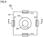
- Fig. 4 is a schematic plan view of the film formation apparatus.
- Fig. 3 shows a cross-section along the line III-III in Fig. 4 .
- a film formation apparatus 200 shown in Figs. 3 and 4 is an AIP apparatus.
- a coating film was formed by using film formation apparatus 200.
- a construction of film formation apparatus 200 will initially be described.
- film formation apparatus 200 includes a chamber 201.
- Chamber 201 is provided with a gas introduction port 202 for introducing source gas into chamber 201 and a gas emission port 203 for emitting the source gas from chamber 201 to the outside.
- Gas emission port 203 is connected to a not-shown vacuum pump.
- a pressure in chamber 201 is regulated based on an amount of introduction and emission of gas.
- a turntable 204 is arranged in chamber 201.
- a substrate holder 205 for holding substrate 10 is attached to turntable 204.
- Substrate holder 205 is connected to a negative electrode of a bias power supply 206.
- a positive electrode of bias power supply 206 is grounded.
- target materials 211, 212, 213, and 214 are attached to a sidewall of chamber 201.
- target materials 211 and 212 are connected to negative electrodes of direct-current (DC) power supplies 221 and 222, respectively.
- DC power supplies 221 and 222 are variable power supplies and positive electrodes thereof are grounded. This is also the case with target materials 213 and 214, although they are not shown in Fig. 3 . Specific operations will be described below.
- Substrate 10 was held on substrate holder 205.
- a pressure in chamber 201 was regulated to 1.0 ⁇ 10 -4 Pa with the vacuum pump. While turntable 204 was turned, a temperature of substrate 10 was adjusted to 500°C with a heater (not shown) attached to film formation apparatus 200.
- Ar gas was introduced through gas introduction port 202 and a pressure in chamber 201 was regulated to 3.0 Pa. While the pressure was maintained, a voltage of bias power supply 206 was gradually varied and finally adjusted to -1000 V. Then, the surface of substrate 10 was cleaned through first ion bombardment treatment using Ar ions.
- a sintered alloy with which alternate layer 21 having a composition shown in Table 1 below could be formed was prepared as each of target materials 211, 212, 213, and 214.
- Target materials 211, 212, 213, and 214 were set at prescribed positions.
- Nitrogen gas was introduced through gas introduction port 202 and alternate layer 21 was formed while turntable 204 was turned.
- a condition for forming alternate layer 21 is as shown below.
- a surface-coated cutting tool according to sample No. 1 was manufactured as set forth above.
- Table 1 below shows a construction of the coating film.
- a composition and a thickness of each layer shown in Table 1 below were measured with the method described previously.
- sample No. 8 in the substrate cleaning step (S21), after first ion bombardment treatment with Ar ions, second ion bombardment treatment with Cr ions was further performed. Alternate layer 21 was formed on a surface subjected to such treatment. Namely, for sample No. 8, the adhesive layer forming step (S22) was performed. A surface-coated cutting tool according to sample No. 8 was manufactured similarly to sample No. 1 except for this aspect. Table 2 below shows a composition and a thickness of adhesive layer 22 in sample No. 8. Table 2 below shows an occupancy by WC particles in a portion where substrate 10 and adhesive layer 22 were in contact with each other. These values were measured with the method described previously.
- Second Composition Ti a Al b Si c N Ti d Al e Si f N a b c d e f d-a b-e [nm] [nm] [-] [ ⁇ m] 1 0.40 0.60 0 0.45 0.55 0 0.05 0.05 1 1 3000 3 2 0.40 0.60 0 0.45 0.55 0 0.05 0.05 200 200 15 3 3 0.40 0.60 0 0.45 0.55 0 0.05 0.05 10 10 300 3 4 0.35 0.65 0 0.55 0.45 0 0.20 0.20 10 10 300 3 5 0.40 0.60 0 0.50 0.50 0 0.10 0.10 10 10 300 3 6 0.30 0.60 0.10 0.35 0.55 0.10 0.05 0.05 10 10 300 3 7 0.39 0.60 0.01 0.44 0.55 0.01 0.05 0.05 10 10 300 3 8 0.40 0.60 0 0.45 0.55
- a lifetime of the tool of each sample was evaluated in a cutting test. Specifically, wet intermittent cutting was performed under cutting conditions below and a cutting distance until the tool was chipped was measured. Table 2 above shows results. A longer cutting distance in Table 2 indicates a longer lifetime of the tool.
- coating film 20 included alternate layer 21.
- first layer 1 and second layer 2 included in alternate layer 21 were considered as being close to each other in composition to such an extent that delamination could be suppressed and as being different from each other in composition to such an extent that propagation of a crack could be suppressed.
- Nos. 1 and 2 were shorter in lifetime of the tool than Nos. 3 to 13, although coating film 20 included alternate layer 21 in Nos. 1 and 2.
- No. 1 is considered as being lower in effect of suppression of propagation of a crack because of too small a thickness of first layer 1 and second layer 2 and resultant mixing between first layer 1 and second layer 2.
- No. 2 is considered as being too large in thickness of first layer 1 and second layer 2, which resulted in tendency of delamination between first layer 1 and second layer 2.
- samples Nos. 8 to 13 were longer in lifetime of the tool than samples Nos. 3 to 7.
- Adhesiveness between substrate 10 and coating film 20 is considered to have improved owing to coating film 20 including adhesive layer 22.
Landscapes
- Chemical & Material Sciences (AREA)
- Engineering & Computer Science (AREA)
- Mechanical Engineering (AREA)
- Chemical Kinetics & Catalysis (AREA)
- Materials Engineering (AREA)
- Metallurgy (AREA)
- Organic Chemistry (AREA)
- Inorganic Chemistry (AREA)
- Drilling Tools (AREA)
- Cutting Tools, Boring Holders, And Turrets (AREA)
- Physical Vapour Deposition (AREA)
- Milling, Broaching, Filing, Reaming, And Others (AREA)
Abstract
Description
- The present disclosure relates to a surface-coated cutting tool.
- The present application claims priority to Japanese Patent Application No.
2016-083780 filed on April 19, 2016 - Japanese Patent Laying-Open No.
2002-096205 2011-224715 -
- PTD 1: Japanese Patent Laying-Open No.
2002-096205 - PTD 2: Japanese Patent Laying-Open No.
2011-224715 - A surface-coated cutting tool according to the present disclosure includes a substrate and a coating film formed on a surface of the substrate. The coating film includes an alternate layer. The alternate layer includes a first layer having a first composition and a second layer having a second composition. The alternate layer is formed by alternately stacking at least one first layer and at least one second layer. The first layer and the second layer each have a thickness not smaller than 2 nm and not greater than 100 nm.
- The first composition is expressed as TiaAlbSicN (0.25 ≤ a ≤ 0.45, 0.55 ≤ b ≤ 0.75, 0 ≤ c ≤ 0.1, a+b+c = 1). The second composition is expressed as TidAleSifN (0.35 ≤ d ≤ 0.55, 0.45 ≤ e ≤ 0.65, 0 ≤ f ≤ 0.1, d+e+f = 1). The first composition and the second composition satisfy a condition of 0.05 ≤ d-a ≤ 0.2 and 0.05 ≤ b-e ≤ 0.2.
-
-
Fig. 1 is a schematic partial cross-sectional view showing one example of a construction of a surface-coated cutting tool according to an embodiment of the present disclosure. -
Fig. 2 is a flowchart showing overview of a method of manufacturing a surface-coated cutting tool according to the embodiment of the present disclosure. -
Fig. 3 is a schematic cross-sectional view of a film formation apparatus. -
Fig. 4 is a schematic plan view of the film formation apparatus. - Environments for surface-coated cutting tools change each day. In particular, in recent years, there are a wider variety of work materials with the emergence of new materials and a speed of working (a cutting speed and a feed rate) is noticeably high. Demands for the surface-coated cutting tools have thus increasingly become high.
- For example, a nickel (Ni)-based heat-resistant alloy has been developed and put into industrial use. The Ni-based heat-resistant alloy is a new material excellent in heat resistance. In contrast, however, the Ni-based heat-resistant alloy is what is called a difficult-to-cut material, and a lifetime of a tool tends to be short in cutting thereof.
- In cutting of a difficult-to-cut material such as the Ni-based heat-resistant alloy, increase in temperature at a cutting edge of the tool is noticeable. As a speed of working is higher, a temperature at the cutting edge of the tool further becomes higher. Therefore, development of a coating film exhibiting wear resistance and oxidation resistance even in a high-temperature environment has been demanded.
- According to
PTD 1, oxidation resistance is improved and deterioration of the coating film at a high temperature is suppressed by adding silicon (Si) to a TiAlN (titanium aluminum nitride) coating film. With the TiAlN coating film containing Si, however, a lifetime of the tool may become short due to adhesion fracture. - Adhesion fracture refers to fracture caused by adhesion of a work material to a cutting edge of a tool during cutting and consequent peel-off of the coating film. Adhesion fracture is likely, for example, when a material high in affinity with a material for a tool such as a Ni-based heat-resistant alloy is cut.
- By adding Si to the TiAlN coating film, a hardness of the coating film is improved. Compressive stress, however, tends to remain in the coating film, and adhesiveness inside the coating film tends to lower. Adhesion fracture is thus considered to be likely.
PTD 1 discloses also a construction in which a TiAlSiN layer and a TiAlN layer are stacked. When a TiAlN coating film containing Si is layered to form a multi-layered structure, however, adhesion fracture is considered to be more likely due to delamination. -
PTD 2 has proposed a coating film formed by alternately stacking a thin layer A having a particulate crystal structure of TiAlN and a thin layer B formed of columnar crystals of TiAlN. According toPTD 2, thin layer A and thin layer B are identical to each other in composition, and hence peeling (delamination) between thin layer A and thin layer B can be suppressed. According to this construction, however, since adjacent unit layers (thin layer A and thin layer B) are identical to each other in composition, a crack tends to develop along a crystal grain boundary and propagate between the unit layers. A long crack can thus develop and may lead to fracture. - In view of the above, an object of the present disclosure is to provide a surface-coated cutting tool of which lifetime is improved.
- Embodiments of the present disclosure will initially be listed and described.
- [1] A surface-coated cutting tool includes a substrate and a coating film formed on a surface of the substrate. The coating film includes an alternate layer. The alternate layer includes a first layer having a first composition and a second layer having a second composition. The alternate layer is formed by alternately stacking at least one first layer and at least one second layer. The first layer and the second layer each have a thickness not smaller than 2 nm and not greater than 100 nm.
- The first composition is expressed as TiaAlbSicN (0.25 ≤ a ≤ 0.45, 0.55 ≤ b ≤ 0.75, 0 ≤ c ≤ 0.1, a+b+c = 1). The second composition is expressed as TidAleSifN (0.35 ≤ d ≤ 0.55, 0.45 ≤ e ≤ 0.65, 0 ≤ f ≤ 0.1, d+e+f = 1). The first composition and the second composition satisfy a condition of 0.05 ≤ d-a ≤ 0.2 and 0.05 ≤ b-e ≤ 0.2.
- In the surface-coated cutting tool (which may be abbreviated as a "tool" below) in [1], the first layer and the second layer included in the alternate layer are each a TiAlN layer, and they are close to each other also in composition. Therefore, the alternate layer is macroscopically uniform in composition. The first layer and the second layer, however, are microscopically different in composition from each other.
- Specifically, the first layer and the second layer are TiAlN layers close to each other in composition to such an extent that crystal lattices can be continuous therebetween, and at the same time, they are TiAlN layers different from each other in composition to such an extent that a crack does not propagate between the first layer and the second layer. Therefore, in the alternate layer, both of delamination and propagation of a crack between the first layer and the second layer can be suppressed.
- The first layer and the second layer each have a thickness not smaller than 2 nm and not greater than 100 nm. When the first layer and the second layer each have a thickness smaller than 2 nm, the first layer and the second layer are mixed with each other, and an effect of suppression of propagation of a crack may be lowered. When the first layer and the second layer each have a thickness exceeding 100 nm, an effect of suppression of delamination may be lowered.
- The first layer and the second layer are TiAlN layers higher in composition ratio of aluminum (Al) than titanium (Ti). It has been found that, even though the alternate layer formed by alternately stacking the first layer and the second layer as such substantially contains no Si, sufficient oxidation resistance is exhibited. It has also been found that, with the coating film including the alternate layer, even when compressive stress provided to the coating film is small, the coating film is high in hardness. Lowering in adhesiveness of the coating film can thus be suppressed while wear resistance is maintained.
- [2] The first composition preferably satisfies a condition of 0 < c ≤ 0.05.
- [3] The second composition preferably satisfies a condition of 0 < f ≤ 0.05.
- As set forth above, even though the TiAlN layer higher in composition ratio of Al than Ti contains substantially no Si, sufficient oxidation resistance is exhibited. When the first layer and the second layer contain a trace amount of Si, however, further improvement in oxidation resistance can be expected while a hardness and adhesiveness of the coating film are maintained.
- [4] The substrate preferably contains WC particles. The coating film preferably further includes an adhesive layer. The adhesive layer is interposed between the substrate and the alternate layer and is in contact with both of the substrate and the alternate layer. The adhesive layer has a thickness not smaller than 0.5 nm and not greater than 50 nm. The adhesive layer contains at least one compound selected from the group consisting of a metal carbide, a metal nitride, and a metal carbonitride. The compound contains (i) tungsten (W), (ii) at least one of Al and Si, and (iii) at least one selected from the group consisting of chromium (Cr), Ti, zirconium (Zr), and niobium (Nb).
- By adopting a substrate containing WC particles, improvement in lifetime of the tool can be expected because tungsten carbide (WC) is high in hardness and excellent in wear resistance. With the coating film including the adhesive layer, peeling strength between the substrate and the coating film is improved. It is thus expected that adhesion fracture is suppressed and a lifetime of the tool is further improved.
- The compound contained in the adhesive layer (a metal carbide, a metal nitride, and a metal carbonitride) contains W (a first element) and at least one of Al and Si (a second element). The first element is common to the element in WC particles contained in the substrate, and the second element is common to the element in the alternate layer (TiAlN). Therefore, such an adhesive layer is high in affinity with both of the substrate and the alternate layer and firmly adheres to both of the substrate and the alternate layer.
- Furthermore, the compound contains at least one element (a third element) selected from the group consisting of Cr, Ti, Zr, and Nb. Though a detailed mechanism is not currently clear, a metal carbide, a metal nitride, and a metal carbonitride containing the third element in addition to the first element and the second element have been found to be very high in peeling strength. Therefore, the adhesive layer can exhibit sufficient peeling strength although it is a layer very small in thickness not smaller than 0.5 nm and not greater than 50 nm.
- [5] The adhesive layer preferably contains carbon (C) and nitrogen (N). In a direction of thickness of the adhesive layer, a content of C preferably decreases from a first interface which is an interface between the substrate and the adhesive layer toward a second interface which is an interface between the adhesive layer and the alternate layer and is lowest at the second interface. A content of N preferably increases from the first interface toward the second interface and is highest at the second interface.
- As set forth above, the alternate layer is composed of a nitride. When the substrate contains WC particles, the substrate is composed of a carbide. Therefore, with the adhesive layer containing both of C and N, the adhesive layer can have affinity with both of the substrate and the alternate layer.
- As set forth above, a content of C and N is varied in the direction of thickness of the adhesive layer so that the adhesive layer has a composition closer to a carbide at the interface (the first interface) between the substrate and the adhesive layer, and the adhesive layer has a composition closer to a nitride at the interface (the second interface) between the adhesive layer and the alternate layer. Affinity between the adhesive layer and the substrate and affinity between the adhesive layer and the alternate layer are thus further enhanced. Namely, improvement in peeling strength can be expected.
- [6] In a portion of the substrate in contact with the adhesive layer, the WC particles preferably occupy 80% or more of that portion.
- When the substrate contains WC particles, normally, the substrate contains also a binder component (a binder phase) such as cobalt (Co). In forming an adhesive layer having the composition above, as an occupancy by the WC particles is higher in the portion of the substrate in contact with the adhesive layer, adhesiveness between the substrate and the coating film can be improved, because the adhesive layer is high in affinity with the WC particles among constituent components of the substrate.
- [7] A surface-coated cutting tool includes a substrate and a coating film formed on a surface of the substrate. The coating film includes an alternate layer. The alternate layer includes a first layer having a first composition and a second layer having a second composition. The alternate layer is formed by alternately stacking at least one first layer and at least one second layer. The first layer and the second layer each have a thickness not smaller than 2 nm and not greater than 100 nm.
- The first composition is expressed as TiaAlbSicN (0.25 ≤ a ≤ 0.45, 0.55 ≤ b ≤ 0.75, 0 < c ≤ 0.05, a+b+c = 1). The second composition is expressed as TidAleSifN (0.35 ≤ d ≤ 0.55, 0.45 ≤ e ≤ 0.65, 0 < f ≤ 0.05, d+e+f= 1). The first composition and the second composition satisfy a condition of 0.05 ≤ d-a ≤ 0.2 and 0.05 ≤ b-e ≤ 0.2.
- A surface-coated cutting tool of which lifetime is improved is provided.
- An embodiment of the present disclosure (hereinafter also denoted as the "present embodiment") will be described below. The scope of the claims should not be limited to the description below.
- A shape and an application of a surface-coated cutting tool in the present embodiment are not particularly limited so long as the surface-coated cutting tool is a cutting tool. The surface-coated cutting tool in the present embodiment can be, for example, a drill, an end mill, a throwaway tip for milling, a throwaway tip for turning, a metal saw, a gear cutting tool, a reamer, a tap, or a tip for pin milling of a crankshaft.
-
Fig. 1 is a schematic partial cross-sectional view showing one example of a construction of a surface-coated cutting tool according to the embodiment of the present disclosure. A surface-coatedcutting tool 100 includes asubstrate 10 and acoating film 20 formed on a surface ofsubstrate 10. -
Substrate 10 is not particularly limited.Substrate 10 can be composed, for example, of cemented carbide, cermet, ceramics, a cubic boron nitride sintered material, or a diamond sintered material.Substrate 10 is composed preferably of cemented carbide because cemented carbide is excellent in wear resistance. - Cemented carbide represents a sintered material mainly composed of WC particles. Cemented carbide contains a hard phase and a binder phase. The hard phase contains WC particles. The binder phase binds WC particles to each other. The binder phase contains, for example, Co. The binder phase may further contain, for example, titanium carbide (TiC), tantalum carbide (TaC), or niobium carbide (NbC).
- When a compound is expressed herein with a composition formula without limiting a ratio of constituent elements such as "TiC", the composition formula encompasses all conventionally known compositions (element ratios). The composition here encompasses also a non-stoichiometric composition. For example, an expression "TiC" means not only a stoichiometric composition "Ti1C1" but also a non-stoichiometric composition such as "Ti1C0.8".
- Cemented carbide may contain an impurity inevitably introduced during a process for manufacturing thereof. Furthermore, cemented carbide may contain free carbon or an abnormal layer called a "η layer" in its structure. A surface of cemented carbide may be reformed. For example, cemented carbide may include a beta (β) removal layer on the surface thereof.
- Preferably, cemented carbide contains at least 87 mass % and at most 96 mass % of WC particles and contains at least 4 mass % and at most 13 mass % of Co. The WC particles have an average particle size preferably not smaller than 0.2 µm and not greater than 2 µm.
- Co is softer than WC particles. As will be described later, ion bombardment treatment of a surface of
substrate 10 can remove soft Co. Cemented carbide has the above-described composition and the WC particles have the above-described average particle size so that moderate projections and recesses are provided in the surface from which Co has been removed. It is considered that, by formingcoating film 20 on such a surface, an anchor effect is expressed and adhesiveness betweencoating film 20 andsubstrate 10 is improved. - A size of WC particles refers to a diameter of a circle which circumscribes a two-dimensionally projected image of a WC particle. A particle size is measured with a scanning electron microscope (SEM) or a transmission electron microscope (TEM). Specifically, cemented carbide is cut, and a cut plane is observed with the SEM or the TEM. A diameter of the circle which circumscribes the WC particle in an observed image is regarded as a size of the WC particle. A size of ten or more (preferably fifty or more and more preferably one hundred or more) randomly extracted WC particles is measured in the observed image, and an arithmetic mean value thereof is regarded as an average size of the WC particles. In observation, the cut plane is desirably processed with cross section polisher (CP) or focused ion beam (FIB).
-
Coating film 20 is formed on a surface ofsubstrate 10.Coating film 20 may be formed on a part or the entirety of the surface ofsubstrate 10.Coating film 20 is formed in a portion of the surface ofsubstrate 10 which corresponds at least to a cutting edge. -
Coating film 20 includes analternate layer 21.Coating film 20 may include other layers so long as it includesalternate layer 21.Coating film 20 may include anadhesive layer 22 which will be described later, for example, in a portion thereof in contact withsubstrate 10.Coating film 20 may include on its outermost surface, for example, a coloring layer for determining whether or not the cutting edge has been used. The coloring layer contains, for example, titanium nitride (TiN). A stacked structure ofcoating film 20 does not have to be uniform over theentire coating film 20 but may partially be different. -
Coating film 20 has a thickness preferably not smaller than 0.5 µm and not greater than 15 µm. With coatingfilm 20 having a thickness not smaller than 0.5 µm, a sufficient wear life can be expected. With coatingfilm 20 having a thickness not greater than 15 µm, improvement in chipping resistance can be expected.Coating film 20 has a thickness more preferably not smaller than 0.5 µm and not greater than 10 µm and further preferably not smaller than 0.5 µm and not greater than 5 µm. - A thickness of
coating film 20 and a thickness of each layer (for example, afirst layer 1 and asecond layer 2 which will be described later) included incoating film 20 are measured with the SEM or the TEM. Specifically, a tool is cut, and a thickness ofcoating film 20 and each layer is measured in a cross-section in a direction of thickness of the coating film. A thickness ofcoating film 20 is measured at at least five locations therein, and an arithmetic mean value thereof is adopted as the thickness ofcoating film 20. - A crystal grain which forms
coating film 20 in the present embodiment is desirably a cubic crystal. With the cubic crystal, a hardness tends to be high and a lifetime of the tool tends to be long. When coatingfilm 20 partially contains amorphous crystal, a hardness ofcoating film 20 may lower. -
Alternate layer 21 includesfirst layer 1 having a first composition andsecond layer 2 having a second composition.Alternate layer 21 is formed by alternately stacking at least onefirst layer 1 and at least onesecond layer 2. - So long as
alternate layer 21 includes at least onefirst layer 1 and at least onesecond layer 2, the number of stacked layers is not particularly limited. The number of stacked layers means a total number offirst layers 1 andsecond layers 2 included inalternate layer 21. The number of stacked layers is, for example, approximately not smaller than 5 and not greater than 7500, preferably approximately not smaller than 10 and not greater than 5000, and more preferably approximately not smaller than 20 and not greater than 500. Inalternate layer 21, a layer closest tosubstrate 10 may befirst layer 1 orsecond layer 2. Inalternate layer 21, a layer most distant fromsubstrate 10 may befirst layer 1 orsecond layer 2. -
First layer 1 andsecond layer 2 each have a thickness not smaller than 2 nm and not greater than 100 nm. It is considered that propagation and development of a crack can be suppressed by alternately repeating such thin layers. When a thickness of each offirst layer 1 andsecond layer 2 is smaller than 2 nm,first layer 1 andsecond layer 2 are mixed with each other, and an effect of suppression of propagation of a crack may be lowered. When a thickness offirst layer 1 andsecond layer 2 exceeds 100 nm, an effect of suppression of delamination may be lowered. - In measurement of a thickness of
first layer 1 andsecond layer 2, a magnification for observation with the TEM is set, for example, to approximately 1000000x. The magnification for observation is adjusted as appropriate in accordance with a thickness offirst layer 1 andsecond layer 2. A thickness offirst layer 1 orsecond layer 2 is measured at at least five locations therein, and an arithmetic mean value thereof is adopted as the thickness offirst layer 1 orsecond layer 2. -
First layer 1 andsecond layer 2 each have a thickness preferably not smaller than 2 nm and not greater than 80 nm, more preferably not smaller than 2 nm and not greater than 50 nm, further preferably not smaller than 2 nm and not greater than 30 nm, and most preferably not smaller than 2 nm and not greater than 20 nm. By thus adjusting a thickness offirst layer 1 andsecond layer 2, improvement in effect of suppression of propagation of a crack and effect of suppression of delamination can be expected. -
First layer 1 has a first composition. The first composition is expressed as TiaAlbSicN (0.25 ≤ a ≤ 0.45, 0.55 ≤ b ≤ 0.75, 0 ≤ c ≤ 0.1, a+b+c = 1). -
Second layer 2 has a second composition. The second composition is expressed as TidAleSifN (0.35 ≤ d ≤ 0.55, 0.45 ≤ e ≤ 0.65, 0 ≤ f ≤ 0.1, d+e+f = 1). - The first composition and the second composition satisfy a condition of 0.05 ≤ d-a ≤ 0.2 and 0.05 ≤ b-e ≤ 0.2. With the condition of 0.05 ≤ d-a and 0.05 ≤ b-e being satisfied, the first composition and the second composition can be different from each other to such an extent that propagation of a crack between
first layer 1 andsecond layer 2 can be suppressed. At the same time, with the condition of d-a ≤ 0.2 and b-e ≤ 0.2 being satisfied, the first composition and the second composition can be close to each other to such an extent that delamination betweenfirst layer 1 andsecond layer 2 can be suppressed. The first composition and the second composition satisfy preferably a condition of 0.05 ≤ d-a ≤ 0.1 and 0.05 ≤ b-e ≤ 0.1. The effect of suppression of propagation of a crack and delamination is thus considered to further improve. - In the first composition, "a" may satisfy a condition of 0.30 ≤ a ≤ 0.40 or 0.35 ≤ a ≤ 0.40. "b" may satisfy a condition of 0.60 ≤ b ≤ 0.70 or 0.60 ≤ b ≤ 0.65.
- In the second composition, "d" may satisfy a condition of 0.40 ≤ d ≤ 0.50 or 0.40 ≤ d ≤ 0.45. "e" may satisfy a condition of 0.50 ≤ e ≤ 0.65 or 0.50 ≤ e ≤ 0.55.
-
First layer 1 andsecond layer 2 may each be a layer containing substantially no Si. In the first composition, "c" may be set to zero, and in the second composition, "f" may be set to zero. Preferably, a condition of 0 < c ≤ 0.05 (more preferably 0.01 ≤ c ≤ 0.05) is satisfied and a condition of 0 < f ≤ 0.05 (more preferably 0.01 ≤ f ≤ 0.05) is satisfied. - The first composition and the second composition (that is, a, b, c, d, e, and f) are determined with energy dispersive X-ray spectrometry (EDX). TEM-EDX is used for analysis of the composition. Specifically, five locations randomly extracted from
first layer 1 orsecond layer 2 are subjected to EDX analysis while a cross-section in a direction of thickness ofalternate layer 21 is observed with the TEM. A diameter of a measurement spot is set to 1 nm. Each of a, b, c, d, e, and f is found by calculating an arithmetic mean of a composition ratio of each element obtained from measurement at five locations. - When the number of stacked layers in
alternate layer 21 is smaller than three, one layer infirst layer 1 and one layer insecond layer 2 are subjected to composition analysis to determine the first composition and the second composition. When the number of stacked layers is approximately from three to ten, two layers infirst layer 1 and two layers insecond layer 2 are subjected to composition analysis and the average composition of the two layers is adopted as the first composition or the second composition. When the number of stacked layers is approximately from ten to fifty, five layers infirst layer 1 and five layers insecond layer 2 are subjected to composition analysis and the average composition of the five layers is adopted as the first composition or the second composition. When the number of stacked layers exceeds fifty, ten layers infirst layer 1 and ten layers insecond layer 2 are subjected to composition analysis and the average composition of the ten layers is adopted as the first composition or the second composition. -
Coating film 20 preferably further includesadhesive layer 22.Adhesive layer 22 is interposed betweensubstrate 10 andalternate layer 21.Adhesive layer 22 is in contact with both ofsubstrate 10 andalternate layer 21. In the presence ofadhesive layer 22 betweensubstrate 10 andalternate layer 21, improvement in effect of suppression of adhesion fracture can be expected. -
Adhesive layer 22 contains at least one compound selected from the group consisting of a metal carbide, a metal nitride, and a metal carbonitride. Such a compound contains a first element, a second element, and a third element. W is adopted as the first element. The first element is an element common to an element in WC particles contained insubstrate 10. At least one of Al and Si is adopted as the second element. The second element is an element common to an element in alternate layer 21 (TiAlN). The third element is at least one selected from the group consisting of Cr, Ti, Zr, and Nb. - Specific examples of the metal carbide, the metal nitride, and the metal carbonitride containing the first element, the second element, and the third element include WTiC, WTiN, WTiCN; WCrC, WCrN, WCrCN; WCrTiC, WCrTiN, WCrTiCN; WTiAlC, WTiAlN, WTiAlCN; WTiSiC, WTiSiN, WTiSiCN; WCrTiAlC, WCrTiAlN, WCrTiAlCN; WCrTiSiC, WCrTiSiN, WCrTiSiCN; WTiAlSiC, WTiAlSiN, WTiAlSiCN; WCrTiAlSiC, WCrTiAlSiN, WCrTiAlSiCN; and the aforementioned compound in which the entirety or a part of Cr is substituted with at least one of Zr and Nb.
-
Adhesive layer 22 may contain one compound among them alone, or may contain two or more compounds. Whenadhesive layer 22 contains two or more compounds, the compounds may be in a form of a solid solution. Alternatively, two or more compounds may be present as being stratified inadhesive layer 22. -
Adhesive layer 22 has a thickness preferably not smaller than 0.5 nm and not greater than 50 nm.Adhesive layer 22 composed as above can exhibit sufficient peeling strength so long as it has a thickness not smaller than 0.5 nm. So long asadhesive layer 22 has a thickness not smaller than 0.5 nm, improvement in peeling strength can be expected as the thickness is smaller. It is considered that residual stress is smaller with decrease in thickness. Therefore,adhesive layer 22 has a thickness more preferably not smaller than 0.5 nm and not greater than 40 nm, further preferably not smaller than 0.5 nm and not greater than 20 nm, and most preferably not smaller than 0.5 nm and not greater than 5 nm. A method of measuring a thickness ofadhesive layer 22 is in conformity with the method of measuring a thickness offirst layer 1 andsecond layer 2 described previously. -
Adhesive layer 22 preferably contains C and N. Namely, preferably,adhesive layer 22 contains a metal carbide and a metal nitride, contains a metal carbide and a metal carbonitride, contains a metal nitride and a metal carbonitride, or contains a metal carbonitride. - When
adhesive layer 22 contains C and N, a content of C and N may be varied in a direction of thickness ofadhesive layer 22. Adhesiveness betweensubstrate 10 andcoating film 20 is thus considered to improve, because affinity betweenadhesive layer 22 andsubstrate 10 and affinity betweenadhesive layer 22 andalternate layer 21 are enhanced. The content may be varied in the direction of thickness ofadhesive layer 22 stepwise or in a ramped manner. - In this embodiment, a content of C preferably decreases from a first interface which is an interface between
substrate 10 andadhesive layer 22 toward a second interface which is an interface betweenadhesive layer 22 andalternate layer 21 and is lowest at the second interface. Affinity betweensubstrate 10 containing C andadhesive layer 22 is thus considered to improve. - A content of N preferably increases from the first interface toward the second interface and is highest at the second interface. Affinity between
alternate layer 21 containing N andadhesive layer 22 is thus considered to improve. - Such variation in composition can be realized, for example, by varying a ratio of a flow rate between C source material gas and N source material gas in a process of forming
adhesive layer 22 through vapor deposition. - Composition variation of C and N is checked with TEM-EDX. In a cross-section in the direction of thickness of
adhesive layer 22, a mapping image of C and N is obtained in EDX analysis, and variation in composition is checked in the mapping image. - Adhesiveness between
substrate 10 andcoating film 20 can also be improved by making an occupancy by WC particles higher in a portion ofsubstrate 10 in contact withadhesive layer 22, becauseadhesive layer 22 is high in affinity with WC particles among constituent components ofsubstrate 10. - An occupancy by WC particles can be made relatively higher, for example, by reducing a binder phase (Co or the like) exposed at the surface of
substrate 10. For example, the binder phase can be reduced by subjecting a surface ofsubstrate 10 to ion bombardment treatment which will be described later. - An occupancy by WC particles in the portion of
substrate 10 in contact withadhesive layer 22 is measured as below. Initially, a tool is cut along the direction of thickness ofcoating film 20 and a cross-section of the interface (first interface) betweensubstrate 10 andadhesive layer 22 is obtained. The cross-section is processed as appropriate with FIB. The cross-section is observed with the TEM. In the observed image, a reference line having a length of 3 µm is set along the first interface. A total length of the portion where WC particles andadhesive layer 22 are in contact with each other within the reference line is measured. A percentage of a value calculated by dividing the total length by the length of the reference line represents the occupancy by the WC particles. - The occupancy by WC particles is preferably not lower than 80%. A higher occupancy by the WC particles is desirable. The upper limit of the occupancy may be 100%. The occupancy by the WC particles is more preferably not lower than 85%, further preferably not lower than 90%, and most preferably not lower than 95%.
- The surface-coated cutting tool in the present embodiment described above can be manufactured with a manufacturing method below.
-
Fig. 2 is a flowchart showing overview of a method of manufacturing a surface-coated cutting tool according to the embodiment of the present disclosure. The manufacturing method includes a substrate preparation step (S10) and a coating film forming step (S20). The coating film forming step (S20) includes at least an alternate layer forming step (S23). The coating film forming step (S20) can further include a substrate cleaning step (S21) and an adhesive layer forming step (S22). - In the substrate preparation step (S10),
substrate 10 is prepared. For example, cemented carbide in a prescribed shape is prepared assubstrate 10. Cemented carbide can be prepared with general powder metallurgy. One example of a specific procedure is shown below. - Mixed powders are obtained by mixing WC particles and Co powders with a wet method with the use of a ball mill. For example, ethanol is adopted as a solvent. The mixed powders are dried. A compact is obtained by shaping the dried mixed powders into a prescribed shape. A sintered material (cemented carbide) is obtained by sintering the compact. The sintered material is subjected to prescribed cutting edge working (for example, honing).
Substrate 10 made of cemented carbide is prepared as set forth above. - In the coating film forming step (S20),
coating film 20 is formed on a surface ofsubstrate 10. - In the present embodiment,
coating film 20 is formed preferably with physical vapor deposition (PVD).Coating film 20 may be formed with chemical vapor deposition (CVD).Coating film 20 formed with PVD tends to be less in deterioration at a high temperature. This may be because a highly crystalline compound tends to be generated with PVD as compared with CVD - Specific examples of PVD include arc ion plating (AIP), balanced magnetron sputtering (BMS), and unbalanced magnetron sputtering (UBMS).
- In AIP, arc discharge is caused with a target material being set as a cathode. The target material is thus vaporized and ionized. Then, ions are deposited on a surface of
substrate 10 to which a negative bias voltage is applied. - In BMS, a target material is arranged on a magnetron electrode and gas plasma is generated by using magnetic field of the magnetron electrode. The target material is thus vaporized and ionized. Ions are then deposited on a surface of
substrate 10. UBMS is a method of increasing a frequency of collision of ions againstsubstrate 10 by intentionally disrupting balance of magnetic field in BMS. - AIP is excellent in ratio of ionization of a target material. By adopting AIP here, the substrate cleaning step (S21) to the alternate layer forming step (S23) can be performed in the same film formation apparatus, which is cost efficient.
- In the substrate cleaning step (S21), a surface of
substrate 10 is cleaned. - For example, the surface of
substrate 10 can be cleaned by subjecting the surface ofsubstrate 10 to first ion bombardment treatment with argon (Ar) ions. The binder phase exposed at the surface ofsubstrate 10 can thus be reduced. An occupancy by WC particles can be increased at the interface (first interface) betweenadhesive layer 22 which will be formed later andsubstrate 10. - Since second ion bombardment treatment which will be described later can also be expected to have a cleaning function, an embodiment in which first ion bombardment treatment is not performed depending on a condition is also possible.
- After first ion bombardment treatment, the surface of
substrate 10 may further be subjected to second ion bombardment treatment with one or more metals selected from the group consisting of Cr, Ti, Zr, and Nb being adopted as a target material. Thus, the binder phase exposed at the surface ofsubstrate 10 can further be reduced. The third element (Cr, Ti, Zr, and Nb) ofadhesive layer 22 can be attached in advance to the surface ofsubstrate 10. A thickness ofadhesive layer 22 can be adjusted, for example, based on an amount of attached third element here. - Preferably, Cr is adopted as the target material in second ion bombardment treatment. Cr is a metal which can sublimate. Therefore, Cr is less likely to become molten particles (droplets) during ion bombardment treatment. Therefore, by adopting Cr, roughening of the surface of
substrate 10 brought about by ion bombardment treatment can be suppressed. - In the adhesive layer forming step (S22),
adhesive layer 22 in contact withsubstrate 10 is formed. For example, the second element (Al, Si), Ti, and N are further deposited with AIP on the surface ofsubstrate 10 to which the third element has been attached by second ion bombardment treatment. - A deposition in which the third element and the second element are fused is thus generated. Furthermore, the first element (W) and C are diffused from WC particles into the deposition. Consequently, a metal carbide, a metal nitride, or a metal carbonitride containing the first element, the second element, and the third element is generated and
adhesive layer 22 is formed . - In the alternate layer forming step (S23),
alternate layer 21 is formed on the surface ofsubstrate 10 or the surface ofadhesive layer 22. By formingalternate layer 21 on the surface ofadhesive layer 22,adhesive layer 22 is interposed betweensubstrate 10 andalternate layer 21 and is in contact with both ofsubstrate 10 andalternate layer 21. -
Alternate layer 21 is formed by alternately stacking at least onefirst layer 1 and at least onesecond layer 2.Alternate layer 21 can be formed, for example, with a method as below. - (A) In AIP, a sintered alloy which contains Ti, Al, and Si and is different in particle size among the metals is employed as the target material.
- (B) In AIP, a plurality of target materials (sintered alloys) different in composition are employed.
- (C) In AIP, during film formation, a bias voltage applied to
substrate 10 is varied like pulses. - (D) In AIP, a flow rate of gas is varied.
- (E) In AIP,
substrate 10 is turned and a period of turning is controlled. - Each of methods (A) to (E) alone can allow formation of
alternate layer 21. Combination of methods (A) to (E) can also allow formation ofalternate layer 21. - Surface-coated
cutting tool 100 includingsubstrate 10 andcoating film 20 formed on a surface ofsubstrate 10 can be manufactured as set forth above. - Examples will be described below. The scope of claims should not be limited to the examples below.
- Various surface-coated cutting tools were manufactured and a lifetime of the tools was evaluated as below.
-
Substrate 10 below was prepared.Substrate 10 contained WC particles (90 mass %) and Co (10 mass %). The WC particles had an average particle size of 2 µm. The average particle size of the WC particles was measured with the method described previously. - Tip model No.: SFKN12T3AZTN (manufactured by Sumitomo Electric Hardmetal Corporation)
Material: cemented carbide (ISO P30 grade) -
Fig. 3 is a schematic cross-sectional view of a film formation apparatus.Fig. 4 is a schematic plan view of the film formation apparatus.Fig. 3 shows a cross-section along the line III-III inFig. 4 . Afilm formation apparatus 200 shown inFigs. 3 and4 is an AIP apparatus. In the present example, a coating film was formed by usingfilm formation apparatus 200. A construction offilm formation apparatus 200 will initially be described. - As shown in
Fig. 3 ,film formation apparatus 200 includes achamber 201.Chamber 201 is provided with agas introduction port 202 for introducing source gas intochamber 201 and agas emission port 203 for emitting the source gas fromchamber 201 to the outside.Gas emission port 203 is connected to a not-shown vacuum pump. A pressure inchamber 201 is regulated based on an amount of introduction and emission of gas. - In
chamber 201, aturntable 204 is arranged. Asubstrate holder 205 for holdingsubstrate 10 is attached toturntable 204.Substrate holder 205 is connected to a negative electrode of abias power supply 206. A positive electrode ofbias power supply 206 is grounded. - As shown in
Fig. 4 , a plurality oftarget materials chamber 201. As shown inFig. 3 ,target materials power supplies DC power supplies target materials Fig. 3 . Specific operations will be described below. -
Substrate 10 was held onsubstrate holder 205. A pressure inchamber 201 was regulated to 1.0×10⁻⁴ Pa with the vacuum pump. Whileturntable 204 was turned, a temperature ofsubstrate 10 was adjusted to 500°C with a heater (not shown) attached to filmformation apparatus 200. - Ar gas was introduced through
gas introduction port 202 and a pressure inchamber 201 was regulated to 3.0 Pa. While the pressure was maintained, a voltage ofbias power supply 206 was gradually varied and finally adjusted to -1000 V. Then, the surface ofsubstrate 10 was cleaned through first ion bombardment treatment using Ar ions. - A sintered alloy with which
alternate layer 21 having a composition shown in Table 1 below could be formed was prepared as each oftarget materials Target materials gas introduction port 202 andalternate layer 21 was formed whileturntable 204 was turned. A condition for formingalternate layer 21 is as shown below. - Temperature of substrate: 500°C
Reaction gas pressure: 0.5 to 10 Pa
Bias voltage: -30 V to -800 V
Arc current: 100 A
A reaction gas pressure and a bias voltage were set to constant values within the ranges above or continuously varied in value within the ranges above. - A surface-coated cutting tool according to sample No. 1 was manufactured as set forth above. Table 1 below shows a construction of the coating film. A composition and a thickness of each layer shown in Table 1 below were measured with the method described previously.
- Surface-coated cutting tools according to samples Nos. 2 and 3 were manufactured similarly to sample No. 1 except for change in thickness of
first layer 1, thickness ofsecond layer 2, and the number of stacked layers as shown in Table 1 below. - Surface-coated cutting tools according to samples Nos. 4 to 7 were manufactured similarly to sample No. 3 except for change in composition of a target material (sintered alloy) such that alternate layers each having a composition shown in Table 1 below were formed.
- For sample No. 8, in the substrate cleaning step (S21), after first ion bombardment treatment with Ar ions, second ion bombardment treatment with Cr ions was further performed.
Alternate layer 21 was formed on a surface subjected to such treatment. Namely, for sample No. 8, the adhesive layer forming step (S22) was performed. A surface-coated cutting tool according to sample No. 8 was manufactured similarly to sample No. 1 except for this aspect. Table 2 below shows a composition and a thickness ofadhesive layer 22 in sample No. 8. Table 2 below shows an occupancy by WC particles in a portion wheresubstrate 10 andadhesive layer 22 were in contact with each other. These values were measured with the method described previously. - Surface-coated cutting tools according to samples Nos. 9 to 13 were manufactured similarly to sample No. 8 except for change in composition of the target material (sintered alloy) such that
alternate layers 21 each having a composition shown in Table 1 below andadhesive layer 22 were formed and change in condition for second ion bombardment treatment. - For samples Nos. 14 to 17,
adhesive layer 22 was not formed but a TiAlN-based coating film having a single composition shown in Table 1 below was formed. Surface-coated cutting tools according to samples Nos. 14 to 17 were manufactured similarly to samples Nos. 1 to 7 except for these aspects. In Table 1 below, compositions of the coating films of samples Nos. 14 to 17 are shown in the field of the first layer for the sake of convenience.Table 1 List of Alternate Layer No. Coating Film Alternate Layer First Layer Second Layer Thickness of First Layer Thickness of Second Layer The Number of Stacked Layers Total Thickness First Composition Second Composition TiaAlbSicN TidAleSifN a b c d e f d-a b-e [nm] [nm] [-] [µm] 1 0.40 0.60 0 0.45 0.55 0 0.05 0.05 1 1 3000 3 2 0.40 0.60 0 0.45 0.55 0 0.05 0.05 200 200 15 3 3 0.40 0.60 0 0.45 0.55 0 0.05 0.05 10 10 300 3 4 0.35 0.65 0 0.55 0.45 0 0.20 0.20 10 10 300 3 5 0.40 0.60 0 0.50 0.50 0 0.10 0.10 10 10 300 3 6 0.30 0.60 0.10 0.35 0.55 0.10 0.05 0.05 10 10 300 3 7 0.39 0.60 0.01 0.44 0.55 0.01 0.05 0.05 10 10 300 3 8 0.40 0.60 0 0.45 0.55 0 0.05 0.05 10 10 300 3 9 0.25 0.74 0.01 0.35 0.60 0.05 0.10 0.14 10 10 300 3 10 0.39 0.60 0.01 0.44 0.55 0.01 0.05 0.05 10 10 300 3 11 0.40 0.60 0 0.45 0.55 0 0.05 0.05 10 10 300 3 12 0.40 0.60 0 0.50 0.50 0 0.10 0.10 10 10 300 3 13 0.39 0.60 0.01 0.44 0.55 0.01 0.05 0.05 10 10 300 3 14 1.00 0 0 - - - - - - - - 3 15 0.40 0.60 0 - - - - - - - - 3 16 0.35 0.65 0 - - - - - - - - 3 17 0.39 0.60 0.01 - - - - - - - - 3 Table 2 List of Substrate, Adhesive Layer, and Results of Evaluation No. Substrate Coating Film Lifetime of Tool Occupancy by WC Particles Adhesive Layer Cutting Distance Composition Variation in Content of C, N Thickness [%] [nm] [m] 1 - - - - 600 2 - - - - 600 3 - - - - 800 4 - - - - 700 5 - - - - 800 6 - - - - 700 7 - - - - 900 8 90 W0.40Cr0.25Ti0.15Al0.20CN Yes 40 1000 9 90 W0.40Cr0.25Ti0.10Al0.20Si0.05CN Yes 40 1100 10 90 W0.40Cr0.25Ti0.09Al0.20Si0.01 CN Yes 40 1200 11 90 W0.40Cr0.25Ti0.15Al0.20CN Yes 5 1200 12 90 W0.40Cr0.25Ti0.15Al0.20CN Yes 5 1300 13 90 W0.40Cr0.25Ti0.09Al0.20Si0.01CN Yes 5 1400 14 - - - - 300 15 - - - - 500 16 - - - - 400 17 - - - - 600 - A lifetime of the tool of each sample was evaluated in a cutting test. Specifically, wet intermittent cutting was performed under cutting conditions below and a cutting distance until the tool was chipped was measured. Table 2 above shows results. A longer cutting distance in Table 2 indicates a longer lifetime of the tool.
- Work material: Ni-based heat-resistant alloy
Cutting speed: 40 m/min.
Feed rate: 0.1 mm/blade
Depth of cut ap: 1.0 mm
Depth of cut ae: 50 mm
As shown in Table 2, samples Nos. 3 to 13 achieved an improved lifetime of the tool as compared with other samples. - As shown in Table 1, in samples Nos. 14 to 17, the coating films each had a single composition. Therefore, it is considered that a crack propagated along a grain boundary and the lifetime of the tool was not long.
- In samples Nos. 3 to 13,
coating film 20 includedalternate layer 21. In samples Nos. 3 to 13,first layer 1 andsecond layer 2 included inalternate layer 21 were considered as being close to each other in composition to such an extent that delamination could be suppressed and as being different from each other in composition to such an extent that propagation of a crack could be suppressed. - Nos. 1 and 2 were shorter in lifetime of the tool than Nos. 3 to 13, although coating
film 20 includedalternate layer 21 in Nos. 1 and 2. No. 1 is considered as being lower in effect of suppression of propagation of a crack because of too small a thickness offirst layer 1 andsecond layer 2 and resultant mixing betweenfirst layer 1 andsecond layer 2. No. 2 is considered as being too large in thickness offirst layer 1 andsecond layer 2, which resulted in tendency of delamination betweenfirst layer 1 andsecond layer 2. - As shown in Table 2, samples Nos. 8 to 13 were longer in lifetime of the tool than samples Nos. 3 to 7. Adhesiveness between
substrate 10 andcoating film 20 is considered to have improved owing to coatingfilm 20 includingadhesive layer 22. - The embodiment and the examples disclosed herein are illustrative and non-restrictive in every respect. The technical scope defined by the terms of the claims is intended to include any modifications within the scope and meaning equivalent to the terms of the claims.
- 1 first layer; 2 second layer; 10 substrate; 20 coating film; 21 alternate layer; 22 adhesive layer; 100 surface-coated cutting tool; 200 film formation apparatus; 201 chamber; 202 gas introduction port; 203 gas emission port; 204 turntable; 205 substrate holder; 206 bias power supply; 211, 212, 213, 214 target material; and 221, 222 DC power supply
Claims (7)
- A surface-coated cutting tool comprising:a substrate; anda coating film formed on a surface of the substrate,the coating film including an alternate layer,the alternate layer including a first layer having a first composition and a second layer having a second composition,the alternate layer being formed by alternately stacking at least one first layer and at least one second layer,the first layer and the second layer each having a thickness not smaller than 2 nm and not greater than 100 nm,the first composition being expressed as TiaAlbSicN (0.25 ≤ a ≤ 0.45, 0.55 ≤ b ≤ 0.75, 0 ≤ c ≤ 0.1, a+b+c = 1),the second composition being expressed as TidAleSifN (0.35 ≤ d ≤ 0.55, 0.45 ≤ e ≤ 0.65, 0 ≤ f ≤ 0.1, d+e+f = 1), andthe first composition and the second composition satisfying a condition of 0.05 ≤ d-a ≤ 0.2 and 0.05 ≤ b-e ≤ 0.2.
- The surface-coated cutting tool according to claim 1, wherein
the first composition satisfies a condition of 0 < c ≤ 0.05. - The surface-coated cutting tool according to claim 1 or 2, wherein
the second composition satisfies a condition of 0 < f ≤ 0.05. - The surface-coated cutting tool according to any one of claims 1 to 3, wherein
the substrate contains WC particles,
the coating film further includes an adhesive layer,
the adhesive layer is interposed between the substrate and the alternate layer and is in contact with both of the substrate and the alternate layer,
the adhesive layer has a thickness not smaller than 0.5 nm and not greater than 50 nm,
the adhesive layer contains at least one compound selected from the group consisting of a metal carbide, a metal nitride, and a metal carbonitride, and
the compound containsW,at least one of Al and Si, andat least one selected from the group consisting of Cr, Ti, Zr, and Nb. - The surface-coated cutting tool according to claim 4, wherein
the adhesive layer contains carbon and nitrogen,
in a direction of thickness of the adhesive layer, a content of the carbon decreases from a first interface which is an interface between the substrate and the adhesive layer toward a second interface which is an interface between the adhesive layer and the alternate layer, and is lowest at the second interface, and a content of the nitrogen increases from the first interface toward the second interface and is highest at the second interface. - The surface-coated cutting tool according to claim 4 or 5, wherein
in a portion of the substrate in contact with the adhesive layer, the WC particles occupy 80% or more of that portion. - A surface-coated cutting tool comprising:a substrate; anda coating film formed on a surface of the substrate,the coating film including an alternate layer,the alternate layer including a first layer having a first composition and a second layer having a second composition,the alternate layer being formed by alternately stacking at least one first layer and at least one second layer,the first layer and the second layer each having a thickness not smaller than 2 nm and not greater than 100 nm,the first composition being expressed as TiaAlbSicN (0.25 ≤ a ≤ 0.45, 0.55 ≤ b ≤ 0.75, 0 < c ≤ 0.05, a+b+c = 1),the second composition being expressed as TidAleSifN (0.35 ≤ d ≤ 0.55, 0.45 ≤ e ≤ 0.65, 0 < f ≤ 0.05, d+e+f = 1), andthe first composition and the second composition satisfying a condition of 0.05 ≤ d-a ≤ 0.2 and 0.05 ≤ b-e ≤ 0.2.
Applications Claiming Priority (2)
| Application Number | Priority Date | Filing Date | Title |
|---|---|---|---|
| JP2016083780A JP6737442B2 (en) | 2016-04-19 | 2016-04-19 | Surface coated cutting tool |
| PCT/JP2017/008498 WO2017183327A1 (en) | 2016-04-19 | 2017-03-03 | Surface-coated cutting tool |
Publications (3)
| Publication Number | Publication Date |
|---|---|
| EP3446814A1 true EP3446814A1 (en) | 2019-02-27 |
| EP3446814A4 EP3446814A4 (en) | 2019-11-27 |
| EP3446814B1 EP3446814B1 (en) | 2024-09-04 |
Family
ID=60116819
Family Applications (1)
| Application Number | Title | Priority Date | Filing Date |
|---|---|---|---|
| EP17785670.5A Active EP3446814B1 (en) | 2016-04-19 | 2017-03-03 | Surface-coated cutting tool |
Country Status (6)
| Country | Link |
|---|---|
| US (1) | US11167357B2 (en) |
| EP (1) | EP3446814B1 (en) |
| JP (1) | JP6737442B2 (en) |
| KR (1) | KR102198744B1 (en) |
| CN (1) | CN109070235B (en) |
| WO (1) | WO2017183327A1 (en) |
Cited By (3)
| Publication number | Priority date | Publication date | Assignee | Title |
|---|---|---|---|---|
| US10570501B2 (en) | 2017-05-31 | 2020-02-25 | Kennametal Inc. | Multilayer nitride hard coatings |
| WO2024180128A1 (en) * | 2023-02-28 | 2024-09-06 | Ab Sandvik Coromant | A coated cutting tool |
| WO2025181307A1 (en) * | 2024-02-28 | 2025-09-04 | Ab Sandvik Coromant | A coated cutting tool |
Families Citing this family (12)
| Publication number | Priority date | Publication date | Assignee | Title |
|---|---|---|---|---|
| JPWO2019188967A1 (en) * | 2018-03-27 | 2021-02-12 | 三菱マテリアル株式会社 | Surface coating cutting tool |
| WO2019188783A1 (en) * | 2018-03-27 | 2019-10-03 | 三菱マテリアル株式会社 | Surface-coated cutting tool |
| JP7067691B1 (en) * | 2021-02-17 | 2022-05-16 | 住友電工ハードメタル株式会社 | Cutting tools |
| WO2022176057A1 (en) | 2021-02-17 | 2022-08-25 | 住友電工ハードメタル株式会社 | Cutting tool |
| CN117561134A (en) * | 2021-07-30 | 2024-02-13 | 京瓷株式会社 | Coated tools and cutting tools |
| US20240316651A1 (en) * | 2021-07-30 | 2024-09-26 | Kyocera Corporation | Coated tool and cutting tool |
| JP7607777B2 (en) | 2021-07-30 | 2024-12-27 | 京セラ株式会社 | Coated and cutting tools |
| EP4497522A4 (en) | 2022-03-22 | 2026-02-18 | Mitsubishi Materials Corp | SURFACE-COATED CUTTING TOOL |
| JP7380978B1 (en) | 2022-06-15 | 2023-11-15 | 住友電工ハードメタル株式会社 | Cutting tools |
| CN121038919A (en) | 2023-04-28 | 2025-11-28 | 住友电工硬质合金株式会社 | Cutting tool |
| US12434304B1 (en) | 2024-03-19 | 2025-10-07 | Sumitomo Electric Industries, Ltd. | Cutting tool |
| WO2025196964A1 (en) * | 2024-03-19 | 2025-09-25 | 住友電気工業株式会社 | Cutting tool |
Family Cites Families (11)
| Publication number | Priority date | Publication date | Assignee | Title |
|---|---|---|---|---|
| JP3404012B2 (en) | 2000-09-19 | 2003-05-06 | 日立ツール株式会社 | Hard coating tool |
| US7537822B2 (en) * | 2005-05-26 | 2009-05-26 | Hitachi Tool Engineering, Ltd. | Hard-coated member |
| JP2009061520A (en) * | 2007-09-05 | 2009-03-26 | Mitsubishi Materials Corp | Surface coated cutting tool with excellent wear resistance with high hard coating layer in high speed cutting |
| JP5594575B2 (en) | 2010-04-20 | 2014-09-24 | 三菱マテリアル株式会社 | Surface coated cutting tool with excellent wear resistance due to hard coating layer |
| JP5459507B2 (en) * | 2010-08-09 | 2014-04-02 | 三菱マテリアル株式会社 | Surface coated cutting tool |
| CN102666437B (en) | 2010-10-28 | 2014-03-12 | 住友电工硬质合金株式会社 | Surface-coated sintered compact |
| KR101351845B1 (en) * | 2012-05-02 | 2014-01-16 | 한국야금 주식회사 | Hard coating film for cutting tools |
| KR20170016811A (en) * | 2014-06-06 | 2017-02-14 | 스미또모 덴꼬오 하드메탈 가부시끼가이샤 | Surface-coated tool and method for manufacturing same |
| US10596636B2 (en) | 2015-08-03 | 2020-03-24 | Tungaloy Corporation | Coated cutting tool |
| EP3360631B1 (en) * | 2015-10-07 | 2022-11-16 | Tungaloy Corporation | Coated cutting tool |
| JP6222675B2 (en) * | 2016-03-28 | 2017-11-01 | 住友電工ハードメタル株式会社 | Surface-coated cutting tool and method for manufacturing the same |
-
2016
- 2016-04-19 JP JP2016083780A patent/JP6737442B2/en active Active
-
2017
- 2017-03-03 EP EP17785670.5A patent/EP3446814B1/en active Active
- 2017-03-03 CN CN201780024349.0A patent/CN109070235B/en active Active
- 2017-03-03 KR KR1020187030104A patent/KR102198744B1/en active Active
- 2017-03-03 US US16/092,499 patent/US11167357B2/en active Active
- 2017-03-03 WO PCT/JP2017/008498 patent/WO2017183327A1/en not_active Ceased
Cited By (4)
| Publication number | Priority date | Publication date | Assignee | Title |
|---|---|---|---|---|
| US10570501B2 (en) | 2017-05-31 | 2020-02-25 | Kennametal Inc. | Multilayer nitride hard coatings |
| US11453063B2 (en) | 2017-05-31 | 2022-09-27 | Kennametal Inc. | Multilayer nitride hard coatings |
| WO2024180128A1 (en) * | 2023-02-28 | 2024-09-06 | Ab Sandvik Coromant | A coated cutting tool |
| WO2025181307A1 (en) * | 2024-02-28 | 2025-09-04 | Ab Sandvik Coromant | A coated cutting tool |
Also Published As
| Publication number | Publication date |
|---|---|
| US11167357B2 (en) | 2021-11-09 |
| EP3446814B1 (en) | 2024-09-04 |
| US20190160546A1 (en) | 2019-05-30 |
| KR20180123703A (en) | 2018-11-19 |
| CN109070235A (en) | 2018-12-21 |
| CN109070235B (en) | 2020-04-07 |
| JP2017193004A (en) | 2017-10-26 |
| WO2017183327A1 (en) | 2017-10-26 |
| KR102198744B1 (en) | 2021-01-05 |
| EP3446814A4 (en) | 2019-11-27 |
| JP6737442B2 (en) | 2020-08-12 |
Similar Documents
| Publication | Publication Date | Title |
|---|---|---|
| EP3446814B1 (en) | Surface-coated cutting tool | |
| EP3153259B1 (en) | Surface-coated tool and method for manufacturing same | |
| EP3269479B1 (en) | Surface-coated cutting tool and method for manufacturing same | |
| EP2623241B1 (en) | Cutting tool | |
| KR20150045425A (en) | Surface-coated cutting tool | |
| EP3763465B1 (en) | Surface-coated cutting tool and method for producing same | |
| EP3808477B1 (en) | Surface-coated cutting tool and process for producing same | |
| CN104870127B (en) | Cutting element | |
| EP3395484B1 (en) | Surface-coated cubic boron nitride sintered compact tool | |
| JP2021126738A (en) | Surface coating cutting tool that demonstrates excellent chipping resistance and wear resistance in strong intermittent cutting | |
| EP2551043B1 (en) | Cutting tool | |
| EP3763466B1 (en) | Surface-coated cutting tool and method for producing same | |
| CN107107203A (en) | Surface-coated cutting tool | |
| JP6743349B2 (en) | Cutting tools | |
| JP5035527B2 (en) | Surface coated cutting tool | |
| JP6743350B2 (en) | Cutting tools | |
| JP2005342856A (en) | Cutting tool made of surface-coated cemented carbide that exhibits excellent chipping resistance with a hard coating layer under intermittent heavy cutting conditions | |
| JP2005288668A (en) | Surface-coated cermet cutting tool that exhibits excellent chipping resistance in high-speed heavy cutting of difficult-to-cut materials. |
Legal Events
| Date | Code | Title | Description |
|---|---|---|---|
| STAA | Information on the status of an ep patent application or granted ep patent |
Free format text: STATUS: THE INTERNATIONAL PUBLICATION HAS BEEN MADE |
|
| PUAI | Public reference made under article 153(3) epc to a published international application that has entered the european phase |
Free format text: ORIGINAL CODE: 0009012 |
|
| STAA | Information on the status of an ep patent application or granted ep patent |
Free format text: STATUS: REQUEST FOR EXAMINATION WAS MADE |
|
| 17P | Request for examination filed |
Effective date: 20181002 |
|
| AK | Designated contracting states |
Kind code of ref document: A1 Designated state(s): AL AT BE BG CH CY CZ DE DK EE ES FI FR GB GR HR HU IE IS IT LI LT LU LV MC MK MT NL NO PL PT RO RS SE SI SK SM TR |
|
| AX | Request for extension of the european patent |
Extension state: BA ME |
|
| DAV | Request for validation of the european patent (deleted) | ||
| DAX | Request for extension of the european patent (deleted) | ||
| A4 | Supplementary search report drawn up and despatched |
Effective date: 20191024 |
|
| RIC1 | Information provided on ipc code assigned before grant |
Ipc: C23C 28/00 20060101ALI20191018BHEP Ipc: C23C 14/46 20060101ALI20191018BHEP Ipc: C23C 28/04 20060101ALI20191018BHEP Ipc: C23C 30/00 20060101ALI20191018BHEP Ipc: B23B 27/14 20060101AFI20191018BHEP Ipc: C23C 14/34 20060101ALI20191018BHEP Ipc: C23C 14/06 20060101ALI20191018BHEP Ipc: C23C 14/22 20060101ALI20191018BHEP |
|
| STAA | Information on the status of an ep patent application or granted ep patent |
Free format text: STATUS: EXAMINATION IS IN PROGRESS |
|
| 17Q | First examination report despatched |
Effective date: 20220131 |
|
| REG | Reference to a national code |
Ref country code: DE Ref legal event code: R079 Free format text: PREVIOUS MAIN CLASS: B23B0027140000 Ipc: C23C0028040000 Ref document number: 602017084654 Country of ref document: DE |
|
| RIC1 | Information provided on ipc code assigned before grant |
Ipc: C23C 14/02 20060101ALI20240307BHEP Ipc: C23C 14/32 20060101ALI20240307BHEP Ipc: C23C 30/00 20060101ALI20240307BHEP Ipc: C23C 28/00 20060101ALI20240307BHEP Ipc: C23C 28/04 20060101AFI20240307BHEP |
|
| GRAP | Despatch of communication of intention to grant a patent |
Free format text: ORIGINAL CODE: EPIDOSNIGR1 |
|
| STAA | Information on the status of an ep patent application or granted ep patent |
Free format text: STATUS: GRANT OF PATENT IS INTENDED |
|
| INTG | Intention to grant announced |
Effective date: 20240415 |
|
| P01 | Opt-out of the competence of the unified patent court (upc) registered |
Free format text: CASE NUMBER: APP_35098/2024 Effective date: 20240611 |
|
| GRAS | Grant fee paid |
Free format text: ORIGINAL CODE: EPIDOSNIGR3 |
|
| GRAA | (expected) grant |
Free format text: ORIGINAL CODE: 0009210 |
|
| STAA | Information on the status of an ep patent application or granted ep patent |
Free format text: STATUS: THE PATENT HAS BEEN GRANTED |
|
| AK | Designated contracting states |
Kind code of ref document: B1 Designated state(s): AL AT BE BG CH CY CZ DE DK EE ES FI FR GB GR HR HU IE IS IT LI LT LU LV MC MK MT NL NO PL PT RO RS SE SI SK SM TR |
|
| REG | Reference to a national code |
Ref country code: GB Ref legal event code: FG4D |
|
| REG | Reference to a national code |
Ref country code: CH Ref legal event code: EP |
|
| REG | Reference to a national code |
Ref country code: IE Ref legal event code: FG4D |
|
| REG | Reference to a national code |
Ref country code: DE Ref legal event code: R096 Ref document number: 602017084654 Country of ref document: DE |
|
| REG | Reference to a national code |
Ref country code: SE Ref legal event code: TRGR |
|
| REG | Reference to a national code |
Ref country code: LT Ref legal event code: MG9D |
|
| REG | Reference to a national code |
Ref country code: NL Ref legal event code: MP Effective date: 20240904 |
|
| PG25 | Lapsed in a contracting state [announced via postgrant information from national office to epo] |
Ref country code: NO Free format text: LAPSE BECAUSE OF FAILURE TO SUBMIT A TRANSLATION OF THE DESCRIPTION OR TO PAY THE FEE WITHIN THE PRESCRIBED TIME-LIMIT Effective date: 20241204 |
|
| PG25 | Lapsed in a contracting state [announced via postgrant information from national office to epo] |
Ref country code: GR Free format text: LAPSE BECAUSE OF FAILURE TO SUBMIT A TRANSLATION OF THE DESCRIPTION OR TO PAY THE FEE WITHIN THE PRESCRIBED TIME-LIMIT Effective date: 20241205 Ref country code: FI Free format text: LAPSE BECAUSE OF FAILURE TO SUBMIT A TRANSLATION OF THE DESCRIPTION OR TO PAY THE FEE WITHIN THE PRESCRIBED TIME-LIMIT Effective date: 20240904 Ref country code: PL Free format text: LAPSE BECAUSE OF FAILURE TO SUBMIT A TRANSLATION OF THE DESCRIPTION OR TO PAY THE FEE WITHIN THE PRESCRIBED TIME-LIMIT Effective date: 20240904 |
|
| PG25 | Lapsed in a contracting state [announced via postgrant information from national office to epo] |
Ref country code: BG Free format text: LAPSE BECAUSE OF FAILURE TO SUBMIT A TRANSLATION OF THE DESCRIPTION OR TO PAY THE FEE WITHIN THE PRESCRIBED TIME-LIMIT Effective date: 20240904 |
|
| PG25 | Lapsed in a contracting state [announced via postgrant information from national office to epo] |
Ref country code: LV Free format text: LAPSE BECAUSE OF FAILURE TO SUBMIT A TRANSLATION OF THE DESCRIPTION OR TO PAY THE FEE WITHIN THE PRESCRIBED TIME-LIMIT Effective date: 20240904 |
|
| PG25 | Lapsed in a contracting state [announced via postgrant information from national office to epo] |
Ref country code: HR Free format text: LAPSE BECAUSE OF FAILURE TO SUBMIT A TRANSLATION OF THE DESCRIPTION OR TO PAY THE FEE WITHIN THE PRESCRIBED TIME-LIMIT Effective date: 20240904 |
|
| PG25 | Lapsed in a contracting state [announced via postgrant information from national office to epo] |
Ref country code: RS Free format text: LAPSE BECAUSE OF FAILURE TO SUBMIT A TRANSLATION OF THE DESCRIPTION OR TO PAY THE FEE WITHIN THE PRESCRIBED TIME-LIMIT Effective date: 20241204 Ref country code: ES Free format text: LAPSE BECAUSE OF FAILURE TO SUBMIT A TRANSLATION OF THE DESCRIPTION OR TO PAY THE FEE WITHIN THE PRESCRIBED TIME-LIMIT Effective date: 20240904 |
|
| PG25 | Lapsed in a contracting state [announced via postgrant information from national office to epo] |
Ref country code: RS Free format text: LAPSE BECAUSE OF FAILURE TO SUBMIT A TRANSLATION OF THE DESCRIPTION OR TO PAY THE FEE WITHIN THE PRESCRIBED TIME-LIMIT Effective date: 20241204 Ref country code: PL Free format text: LAPSE BECAUSE OF FAILURE TO SUBMIT A TRANSLATION OF THE DESCRIPTION OR TO PAY THE FEE WITHIN THE PRESCRIBED TIME-LIMIT Effective date: 20240904 Ref country code: NO Free format text: LAPSE BECAUSE OF FAILURE TO SUBMIT A TRANSLATION OF THE DESCRIPTION OR TO PAY THE FEE WITHIN THE PRESCRIBED TIME-LIMIT Effective date: 20241204 Ref country code: LV Free format text: LAPSE BECAUSE OF FAILURE TO SUBMIT A TRANSLATION OF THE DESCRIPTION OR TO PAY THE FEE WITHIN THE PRESCRIBED TIME-LIMIT Effective date: 20240904 Ref country code: HR Free format text: LAPSE BECAUSE OF FAILURE TO SUBMIT A TRANSLATION OF THE DESCRIPTION OR TO PAY THE FEE WITHIN THE PRESCRIBED TIME-LIMIT Effective date: 20240904 Ref country code: GR Free format text: LAPSE BECAUSE OF FAILURE TO SUBMIT A TRANSLATION OF THE DESCRIPTION OR TO PAY THE FEE WITHIN THE PRESCRIBED TIME-LIMIT Effective date: 20241205 Ref country code: FI Free format text: LAPSE BECAUSE OF FAILURE TO SUBMIT A TRANSLATION OF THE DESCRIPTION OR TO PAY THE FEE WITHIN THE PRESCRIBED TIME-LIMIT Effective date: 20240904 Ref country code: ES Free format text: LAPSE BECAUSE OF FAILURE TO SUBMIT A TRANSLATION OF THE DESCRIPTION OR TO PAY THE FEE WITHIN THE PRESCRIBED TIME-LIMIT Effective date: 20240904 Ref country code: BG Free format text: LAPSE BECAUSE OF FAILURE TO SUBMIT A TRANSLATION OF THE DESCRIPTION OR TO PAY THE FEE WITHIN THE PRESCRIBED TIME-LIMIT Effective date: 20240904 |
|
| REG | Reference to a national code |
Ref country code: AT Ref legal event code: MK05 Ref document number: 1720466 Country of ref document: AT Kind code of ref document: T Effective date: 20240904 |
|
| PG25 | Lapsed in a contracting state [announced via postgrant information from national office to epo] |
Ref country code: NL Free format text: LAPSE BECAUSE OF FAILURE TO SUBMIT A TRANSLATION OF THE DESCRIPTION OR TO PAY THE FEE WITHIN THE PRESCRIBED TIME-LIMIT Effective date: 20240904 |
|
| PG25 | Lapsed in a contracting state [announced via postgrant information from national office to epo] |
Ref country code: PT Free format text: LAPSE BECAUSE OF FAILURE TO SUBMIT A TRANSLATION OF THE DESCRIPTION OR TO PAY THE FEE WITHIN THE PRESCRIBED TIME-LIMIT Effective date: 20250106 Ref country code: IS Free format text: LAPSE BECAUSE OF FAILURE TO SUBMIT A TRANSLATION OF THE DESCRIPTION OR TO PAY THE FEE WITHIN THE PRESCRIBED TIME-LIMIT Effective date: 20250104 |
|
| PG25 | Lapsed in a contracting state [announced via postgrant information from national office to epo] |
Ref country code: RO Free format text: LAPSE BECAUSE OF FAILURE TO SUBMIT A TRANSLATION OF THE DESCRIPTION OR TO PAY THE FEE WITHIN THE PRESCRIBED TIME-LIMIT Effective date: 20240904 Ref country code: SM Free format text: LAPSE BECAUSE OF FAILURE TO SUBMIT A TRANSLATION OF THE DESCRIPTION OR TO PAY THE FEE WITHIN THE PRESCRIBED TIME-LIMIT Effective date: 20240904 |
|
| PG25 | Lapsed in a contracting state [announced via postgrant information from national office to epo] |
Ref country code: EE Free format text: LAPSE BECAUSE OF FAILURE TO SUBMIT A TRANSLATION OF THE DESCRIPTION OR TO PAY THE FEE WITHIN THE PRESCRIBED TIME-LIMIT Effective date: 20240904 Ref country code: AT Free format text: LAPSE BECAUSE OF FAILURE TO SUBMIT A TRANSLATION OF THE DESCRIPTION OR TO PAY THE FEE WITHIN THE PRESCRIBED TIME-LIMIT Effective date: 20240904 |
|
| PG25 | Lapsed in a contracting state [announced via postgrant information from national office to epo] |
Ref country code: CZ Free format text: LAPSE BECAUSE OF FAILURE TO SUBMIT A TRANSLATION OF THE DESCRIPTION OR TO PAY THE FEE WITHIN THE PRESCRIBED TIME-LIMIT Effective date: 20240904 |
|
| PG25 | Lapsed in a contracting state [announced via postgrant information from national office to epo] |
Ref country code: SK Free format text: LAPSE BECAUSE OF FAILURE TO SUBMIT A TRANSLATION OF THE DESCRIPTION OR TO PAY THE FEE WITHIN THE PRESCRIBED TIME-LIMIT Effective date: 20240904 Ref country code: IT Free format text: LAPSE BECAUSE OF FAILURE TO SUBMIT A TRANSLATION OF THE DESCRIPTION OR TO PAY THE FEE WITHIN THE PRESCRIBED TIME-LIMIT Effective date: 20240904 |
|
| REG | Reference to a national code |
Ref country code: DE Ref legal event code: R097 Ref document number: 602017084654 Country of ref document: DE |
|
| PG25 | Lapsed in a contracting state [announced via postgrant information from national office to epo] |
Ref country code: DK Free format text: LAPSE BECAUSE OF FAILURE TO SUBMIT A TRANSLATION OF THE DESCRIPTION OR TO PAY THE FEE WITHIN THE PRESCRIBED TIME-LIMIT Effective date: 20240904 |
|
| PLBE | No opposition filed within time limit |
Free format text: ORIGINAL CODE: 0009261 |
|
| STAA | Information on the status of an ep patent application or granted ep patent |
Free format text: STATUS: NO OPPOSITION FILED WITHIN TIME LIMIT |
|
| 26N | No opposition filed |
Effective date: 20250605 |
|
| PG25 | Lapsed in a contracting state [announced via postgrant information from national office to epo] |
Ref country code: MC Free format text: LAPSE BECAUSE OF FAILURE TO SUBMIT A TRANSLATION OF THE DESCRIPTION OR TO PAY THE FEE WITHIN THE PRESCRIBED TIME-LIMIT Effective date: 20240904 |
|
| REG | Reference to a national code |
Ref country code: CH Ref legal event code: H13 Free format text: ST27 STATUS EVENT CODE: U-0-0-H10-H13 (AS PROVIDED BY THE NATIONAL OFFICE) Effective date: 20251023 |
|
| PG25 | Lapsed in a contracting state [announced via postgrant information from national office to epo] |
Ref country code: LU Free format text: LAPSE BECAUSE OF NON-PAYMENT OF DUE FEES Effective date: 20250303 |
|
| GBPC | Gb: european patent ceased through non-payment of renewal fee |
Effective date: 20250303 |
|
| REG | Reference to a national code |
Ref country code: BE Ref legal event code: MM Effective date: 20250331 |
|
| PG25 | Lapsed in a contracting state [announced via postgrant information from national office to epo] |
Ref country code: GB Free format text: LAPSE BECAUSE OF NON-PAYMENT OF DUE FEES Effective date: 20250303 |
|
| PG25 | Lapsed in a contracting state [announced via postgrant information from national office to epo] |
Ref country code: FR Free format text: LAPSE BECAUSE OF NON-PAYMENT OF DUE FEES Effective date: 20250331 |
|
| PG25 | Lapsed in a contracting state [announced via postgrant information from national office to epo] |
Ref country code: BE Free format text: LAPSE BECAUSE OF NON-PAYMENT OF DUE FEES Effective date: 20250331 |
|
| PG25 | Lapsed in a contracting state [announced via postgrant information from national office to epo] |
Ref country code: CH Free format text: LAPSE BECAUSE OF NON-PAYMENT OF DUE FEES Effective date: 20250331 |
|
| PG25 | Lapsed in a contracting state [announced via postgrant information from national office to epo] |
Ref country code: IE Free format text: LAPSE BECAUSE OF NON-PAYMENT OF DUE FEES Effective date: 20250303 |
|
| PGFP | Annual fee paid to national office [announced via postgrant information from national office to epo] |
Ref country code: SE Payment date: 20260211 Year of fee payment: 10 |
|
| PGFP | Annual fee paid to national office [announced via postgrant information from national office to epo] |
Ref country code: DE Payment date: 20260128 Year of fee payment: 10 |