EP3446342B1 - Gekoppelter quanten-dot-memristor - Google Patents
Gekoppelter quanten-dot-memristor Download PDFInfo
- Publication number
- EP3446342B1 EP3446342B1 EP17719893.4A EP17719893A EP3446342B1 EP 3446342 B1 EP3446342 B1 EP 3446342B1 EP 17719893 A EP17719893 A EP 17719893A EP 3446342 B1 EP3446342 B1 EP 3446342B1
- Authority
- EP
- European Patent Office
- Prior art keywords
- quantum
- electrode
- memristor
- dot
- tunnelling
- Prior art date
- Legal status (The legal status is an assumption and is not a legal conclusion. Google has not performed a legal analysis and makes no representation as to the accuracy of the status listed.)
- Active
Links
Images




Classifications
-
- H—ELECTRICITY
- H10—SEMICONDUCTOR DEVICES; ELECTRIC SOLID-STATE DEVICES NOT OTHERWISE PROVIDED FOR
- H10N—ELECTRIC SOLID-STATE DEVICES NOT OTHERWISE PROVIDED FOR
- H10N70/00—Solid-state devices having no potential barriers, and specially adapted for rectifying, amplifying, oscillating or switching
- H10N70/801—Constructional details of multistable switching devices
- H10N70/881—Switching materials
- H10N70/883—Oxides or nitrides
-
- G—PHYSICS
- G11—INFORMATION STORAGE
- G11C—STATIC STORES
- G11C13/00—Digital stores characterised by the use of storage elements not covered by groups G11C11/00, G11C23/00, or G11C25/00
- G11C13/0002—Digital stores characterised by the use of storage elements not covered by groups G11C11/00, G11C23/00, or G11C25/00 using resistive RAM [RRAM] elements
- G11C13/0007—Digital stores characterised by the use of storage elements not covered by groups G11C11/00, G11C23/00, or G11C25/00 using resistive RAM [RRAM] elements comprising metal oxide memory material, e.g. perovskites
-
- H—ELECTRICITY
- H10—SEMICONDUCTOR DEVICES; ELECTRIC SOLID-STATE DEVICES NOT OTHERWISE PROVIDED FOR
- H10N—ELECTRIC SOLID-STATE DEVICES NOT OTHERWISE PROVIDED FOR
- H10N70/00—Solid-state devices having no potential barriers, and specially adapted for rectifying, amplifying, oscillating or switching
- H10N70/011—Manufacture or treatment of multistable switching devices
- H10N70/021—Formation of switching materials, e.g. deposition of layers
-
- H—ELECTRICITY
- H10—SEMICONDUCTOR DEVICES; ELECTRIC SOLID-STATE DEVICES NOT OTHERWISE PROVIDED FOR
- H10N—ELECTRIC SOLID-STATE DEVICES NOT OTHERWISE PROVIDED FOR
- H10N70/00—Solid-state devices having no potential barriers, and specially adapted for rectifying, amplifying, oscillating or switching
- H10N70/20—Multistable switching devices, e.g. memristors
-
- H—ELECTRICITY
- H10—SEMICONDUCTOR DEVICES; ELECTRIC SOLID-STATE DEVICES NOT OTHERWISE PROVIDED FOR
- H10N—ELECTRIC SOLID-STATE DEVICES NOT OTHERWISE PROVIDED FOR
- H10N70/00—Solid-state devices having no potential barriers, and specially adapted for rectifying, amplifying, oscillating or switching
- H10N70/20—Multistable switching devices, e.g. memristors
- H10N70/253—Multistable switching devices, e.g. memristors having three or more electrodes, e.g. transistor-like devices
-
- H—ELECTRICITY
- H10—SEMICONDUCTOR DEVICES; ELECTRIC SOLID-STATE DEVICES NOT OTHERWISE PROVIDED FOR
- H10N—ELECTRIC SOLID-STATE DEVICES NOT OTHERWISE PROVIDED FOR
- H10N70/00—Solid-state devices having no potential barriers, and specially adapted for rectifying, amplifying, oscillating or switching
- H10N70/801—Constructional details of multistable switching devices
- H10N70/841—Electrodes
-
- G—PHYSICS
- G11—INFORMATION STORAGE
- G11C—STATIC STORES
- G11C2216/00—Indexing scheme relating to G11C16/00 and subgroups, for features not directly covered by these groups
- G11C2216/02—Structural aspects of erasable programmable read-only memories
- G11C2216/08—Nonvolatile memory wherein data storage is accomplished by storing relatively few electrons in the storage layer, i.e. single electron memory
Definitions
- the present invention relates to novel memristive devices, uses thereof, and processes for their preparation.
- the devices of the invention have been made possible by the development of a new, generic, quantum-mechanical model of memristive systems which provides new insights into their behaviour.
- This model described herein, opens the way to novel memristive devices which exploit behaviours explained for the first time by the new model.
- the new model has led to the surprising insight that certain behaviours which are often regarded as frustrations in experimental work may in fact be usefully harnessed as the basis of memristive function.
- Memristive systems are generalisations of memristors, which are resistors with memory.
- Resistors, capacitors and inductors are the three fundamental circuit elements that are familiar from high school level electronics.
- Leon Chua postulated a fourth two-terminal circuit element characterized by a relationship between charge and flux linkage. Predicting that conductance would depend on the history of current flow through it, he dubbed it memristor for memory and resistor. This is described in L. O. Chua, Memristor-The Missing Circuit Element, EEE Trans. Circuit Theory 18 507 (1971 ).
- the resistance of a memristor depends on its history, i.e. on what current has passed through the memristive device previously. This results in a pinched hysteresis, or Lissajous loop. This time dependent current-voltage characteristic can then be incorporated into a circuit to serve as a memory, as described in, for example, Nonvolatile memristor memory: device characteristics and design implications by Ho et al., Proceedings of the 2009 International Conference on Computer-Aided Design, pages 485-490 (ISBN 978-1-60558-800-1, doi 10.1145/1687399.1687491 ), the contents of which are incorporated herein by reference.
- memristive systems As with many other electronic devices, the behaviour of memristive systems is increasingly affected by quantum phenomena as the device size shrinks to ever smaller dimensions. Memristors based on ionic motion can be scaled down to less than 10 nm, and other candidates of memristive systems include even smaller objects, e.g. molecules. At the nanoscale, electron transport through devices is strongly influenced by the discrete energy spectrum and interference effect, which may even emerge at room temperature in certain molecules. It is therefore crucial to understand the non-classical behaviour that emerges in nanoscale memristive systems.
- memristive device and “memristive system” are employed interchangeably and are intended to refer to quantum memristive devices: that is, memristive devices whose characteristics and behaviour can be explained only at a quantum-mechanical level.
- a memristive device can be considered as a quantum open system: the internal state of the device interacts with the environment, typically the electrodes, such that the internal state affects the electron transport (the resistance), and the evolution of the internal state depends on external signals (current and voltage).
- An example of such an open quantum system is a pair of capacitively-coupled quantum dots (a "double quantum dot device” or “double dot device”), where only one dot participates in the electron transport while the other (called the control dot) controls the transport via the capacitive coupling.
- the environment electrodes
- the environment is configured such that the evolution of the control dot depends on the applied voltage.
- capacitor coupling is a well known term in the field of electronic circuit design and the conventional meaning is adopted herein. In brief, it means that energy is transferred by means of displacement currents induced by existing electric fields between nodes of a circuit or circuits. Further details can be found in standard electrical engineering or circuit design handbooks.
- Quantum dots based on nanoparticles are well-known for optical applications owing to their bright, pure colours along with their ability to emit a wide variety of colours of light coupled with their high efficiencies, long lifetimes and high extinction coefficients.
- Single quantum dot flash memory devices are known in the art ( A Marent et al., Semicond. Sci. Technol., 26, (2011), 014026 ), as are multiple coupled quantum dot devices, such as EP 1 262 911 , where a quantum computer comprised of two unequally sized quantum dots coupled by tunnelling junctions, and EP 1 198 008 , in which a device intended to be used for quantum information processing comprised of capacitively coupled quantum dots is described.
- a double quantum dot device exhibits current-voltage hysteresis curves, which are a characteristic property of memristive systems.
- the current in quantum memristive systems shows stochastic behaviour and may not converge to a periodic curve under periodic driving due to quantum jumps between different values of the quantised conductance.
- Room temperature operation of the devices of the invention could potentially be achieved in ultra-scale semiconductor devices or by using single-molecule transistors. While device geometries employing capacitive coupling between two quantum dots are known, the use of a double quantum dot system as a memristive device has not been explored to date and thus memristors based on capacitively-coupled double quantum dot systems have also been unknown before now.
- the present invention provides a simple and practical scheme for realising memristive systems with quantum dots.
- the present invention harnesses a phenomenon that is commonly seen as a bane of nanoelectronics, i.e. switching of a trapped charge in the vicinity of the device, and demonstrates that this can be put to good use in the realisation of a quantum-dot-based memristive system.
- Quantum-dot memristive systems as described herein have hysteresis current-voltage characteristics and quantum jump induced stochastic behaviour.
- Quantum dots display unique electronic properties which are intermediate between those of bulk semiconductors and discrete molecules. Electrons in quantum dots are confined in a small space which leads to the quantum dot behaving as a "quantum box” similar to the well-known "particle in a box” model as described in, for example, Molecular Quantum Mechanics by P. W. Atkins and R. S. Friedman (Oxford University Press, 5th ed. 2010 ).
- the exciton Bohr radius is the average distance between the electron in the conduction band of the semiconductor and the hole it leaves behind in the valence band of the semiconductor
- the discrete, quantized energy levels of quantum dots relate their behaviour more closely to atoms than bulk materials.
- the size of the quantum dot decreases, the difference in energy between the highest valence band and the lowest conduction band increases.
- quantum dots are tiny particles (nanocrystals) of metal or semiconducting material. Such particles typically have a diameter of about 2 to about 10 nm, and/or an overall content of about 10 to about 50 atoms or about 10 to about 50 molecules. The unique electronic properties of such particles are therefore partly the result of the unusually high surface-to-volume ratios of such particles. Quantum dots of the particulate (nanocrystalline) type may be used in the memristive devices of the present invention.
- Particulate quantum dots can be classified into different types based on their composition and structure, as described below. All such quantum dots may suitably be applied in the devices of the present invention.
- quantum dots are not restricted to being particulate (atomic or molecular nanocrystalline) QDs such as those described above.
- a QD may be any structure which causes electron confinement in a region which behaves as a "quantum box", i.e. any structure which leads to quantisation of energy levels.
- the quantum dots employed in the memristive devices of the invention may be single atoms or single molecules.
- the quantum dots may be nanocrystalline. Where atomic, molecular or nanocrystalline quantum dots are employed, these may be anchored to their respective electrode or electrodes using linker molecules which permit electron tunnelling between the QD and the anchored electrode(s).
- the quantum dots may be metallic or semiconductor "islands" which may be lithographically or electrostatically defined.
- the quantum dots may be formed by individual atoms, molecules or nanoparticles.
- the quantum dots employed in the memristive devices of the invention may be regions of material which are formed from the same piece of material as at least one electrode (e.g. a single piece of material comprising a source electrode, drain electrode and a quantum dot, or a single piece of material comprising a reservoir electrode and a quantum dot).
- a quantum dot may be defined as a region of that material which causes electron confinement locally such that the region behaves as a quantum box.
- the quantum dot may be formed by creating constrictions in the material (e.g.
- Such barriers may be created, for example, by using notches in the material.
- Such constrictions or notches may be formed lithographically, for example by creating constrictions in a lithographic channel. These notches or constrictions create a tunnelling barrier which causes the region of material on one side of that barrier to behave as a quantum dot and the region of material on another side of that barrier to behave as an electrode, such that electrons can travel between the quantum dot and the electrode only via quantum tunnelling.
- Any suitable lithographic technique may be employed, such as electron beam or optical lithography, wet chemical etching, reactive ion etching or plasma etching.
- Suitable materials for use in such embodiments include metals, semiconductors such as Si or gallium arsenide, or two dimensional materials such as graphene.
- the quantum dots may be regions of a continuous material which are caused to behave as quantum dots by the creation of electrostatically-induced tunnel barriers. These barriers act to separate the QD region from the remainder of the material such that the QD region acts as a quantum box and such that electrons can travel in and out of the QD region only via quantum tunnelling. Such barriers can be employed in lithographically defined channels such as those described above, for example in place of constrictions or notches such that the QD region is defined by a gate electrode which alters the electrostatic properties of the material to induce QD behaviour instead of using a physical constriction to induce this. Electrostatically-induced tunnel barriers may also be employed to create one or more QD regions in a two-dimensional electron/hole gas such as a patterned semiconductor material or a semiconductor heterostructure.
- the evolution of the state is controlled by the voltage, and the state equation [Equation (2)] is assumed to have a unique solution for any initial condition.
- the coupling between the system (device) and the environment is weak, the influence of the system on the environment is small, and the state of the total system is approximately a tensor product ⁇ ⁇ ⁇ S ⁇ ⁇ E , where ⁇ S is the state of the system and ⁇ E is the state of the environment.
- the present invention relates to memristive systems as defined above, i.e. quantum mechanical memristive systems, which may also be called “quantum memristive systems”, “quantum resistive memory systems” or “quantum memristors”.
- quantum mechanical memristive systems which may also be called “quantum memristive systems”, “quantum resistive memory systems” or “quantum memristors”.
- Quantum dots have discrete energy spectra due to electron confinement in all three spatial directions. Coulomb repulsion between electrons in a quantum dot leads to an increasing energy cost for adding more electrons to the dot.
- Coulomb repulsion energy are large enough so that each quantum dot can be treated as a single-level system, i.e. each dot has only two states: empty or occupied with one electron.
- This simplified model allows the behaviour of a memristive system to be mathematically described relatively concisely.
- the present invention is not limited only to those memristive devices which are precisely described by such a model.
- the present invention also encompasses memristive devices in which at least one quantum dot (or both quantum dots) behaves as a two-level system.
- Memristive devices according to the invention are quantum memristive devices comprising two quantum dots, QD1 and QD2.
- the memristive devices of the invention further comprise a first electrode and a second electrode, which may also be referred to as "terminals".
- the first and second electrodes are coupled to the first quantum dot QD1 via quantum tunnelling.
- FIG. 1(a) An embodiment of such a device is illustrated in Fig. 1(a) .
- the first and second electrodes are coupled to QD1 via quantum tunnelling with tunnelling strength ⁇ 1 .
- the input is the voltage V applied on these two terminals, and the output is the current I going through QD1.
- the tunnelling strength may be determined by employing one or more depletion gates, such as those shown as LD 1 and RD 1 in Figure 1(b) .
- any spatial arrangement of QD1 and the electrodes is permissible, provided that a voltage V is applied across the first and second electrodes such that one electrode has a positive electrochemical potential (this is termed the source electrode or “electrode-L” or “L electrode”) and the other a negative electrochemical potential (this is termed the drain electrode or "electrode-R” or “R electrode”) with respect to QD1, and provided that both first and second electrodes are coupled to the first quantum dot QD1 with tunnelling strength ⁇ 1 .
- electrode-L may be connected to a local gate of QD2. Such an embodiment is shown in Figure 1(b) , where electrode-L is connected to LD2 (a local gate of QD2) rather than to a capacitively coupled lead as shown in Figure 1(a) .
- V / 2 and the electrochemical potential in the second electrode (electrode-R) is ⁇ R -
- the energy level of QD1 is within the window defined by ⁇ L and ⁇ R [see Fig. 1(c) ]
- electrons can go through QD1 via tunnelling couplings with the terminals; when the energy level of QD1 is out of the window, the current decreases exponentially with the energy due to the Fermi-Dirac distribution of electrons in terminals.
- the current can be switched on and off by changing the energy level of QD1.
- the energy level of QD1 can be changed by varying the potential at the first and/or second electrodes, and is also affected by the state of QD2 as described below.
- E 1 is the energy of the QD1 level
- f(E) [1 +exp( E / k B T )] -1 (where k B is the Boltzmann constant)
- T is the temperature.
- Quantum dot QD1 is capacitively coupled to a second quantum dot QD2.
- the state of QD2 can affect the energy level of QD1.
- G ON e ⁇ 1 f ⁇ ⁇ L ⁇ f ⁇ ⁇ R / 2 V
- G OFF e ⁇ 1 f E C ⁇ ⁇ L ⁇ f E C ⁇ ⁇ R / 2 V , respectively, for an empty and occupied QD2.
- the relaxation time of QD1 is ⁇ ⁇ 1 -1 .
- the voltage is switched with a frequency much smaller than ⁇ 1 .
- the conductance is always finite, i.e. the condition I
- ⁇ 1 will be of the order of 1 THz, which corresponds to an energy of about 1 meV. This is much higher than the typical switching frequency of electronic circuits, which is of the order of 1 GHz or below.
- QD2 is capacitively coupled to one of the two terminals [e.g. in one embodiment electrode-L, as illustrated in Fig. 1(a) , although in an alternative embodiment QD2 may be capacitively coupled to electrode-R.].
- Electrode-L is coupled to both QD1 and QD2, being coupled to QD1 by quantum tunnelling and to QD2 by capacitive coupling.
- the electrode which is coupled to both QD1 and to QD2 may be referred to as "the source electrode", thus in the embodiment shown in Figure 1 , electrode-L is the source electrode.
- both QD1 and QD2 are coupled to the source electrode using quantum tunnelling but preferably QD1 is coupled to the source electrode by quantum tunnelling and QD2 is coupled to the source electrode capacitively. This is shown in the embodiment of Figure 1 .
- the devices of the invention further comprise a "bath electrode” or “reservoir electrode”, also termed “electrode-B” as shown by way of illustration in Figure 1(a) .
- This electrode is coupled to QD2 by quantum tunnelling.
- QD2 is coupled to the electrode-B with tunnelling strength ⁇ 2 [see Fig. 1(a) ].
- the tunnelling coupling strength depends on the energy of the QD2 level. Therefore, the evolution of QD2 is controlled by the voltage.
- the material of which electrode-B is made, and the potential at which it is held, can affect the behaviour of the memristive device. For example, if E 2 is far above, or far below, the Fermi energy of electrode-B, the tunnelling strength ⁇ 2 could be a constant. If E 2 is far above the Fermi energy of electrode-B, then ⁇ in will be zero. If E 2 is far below the Fermi energy, ⁇ out will be zero. Thus, a requirement for a functioning double quantum dot memristor is that the distribution of electrons around energy E 2 varies with the value of E 2 . This can be ensured by appropriate choice of the electrode-B material.
- Suitable electrode-B materials will be readily determined by the skilled person having regard to the mathematical model described herein and their knowledge of the band structure of conventional materials.
- Non-limiting examples of the material for electrode-B include, for instance, any suitable semiconductor, or a graphene nanoribbon.
- electrode-B may be earthed. This may be desirable where the capacitive coupling between electrode-B and QD2 is otherwise not weak enough to be neglected.
- the present invention provides a quantum memristor, comprising:
- Capacitive coupling and quantum-tunnelling-mediated coupling are both functions of distance, among other variables.
- the tunnelling current drops off exponentially with increasing distance (e.g. distance between a quantum dot and an electrode) whereas capacitive coupling varies linearly with distance, increasing linearly in strength as distance decreases.
- capacitive coupling varies linearly with distance, increasing linearly in strength as distance decreases.
- QD1 and QD2 may independently be chosen from any of the known types of quantum dot. They may be identical to one another or different to one another, e.g. of the same material or of different materials. In particular, QD1 and QD2 may independently be the same size and/or shape as one another or may be different sizes and/or shapes to one another. QD1 and QD2 may independently be of the same material as one another or different material to one another. Possible materials for QD1 and/or QD2 include, but are not limited to, materials selected from among group IV semiconductors Si, Ge, or heterostructures of group IV semiconductors (SiGe); group III-V semiconductors, e.g.
- QD1 and QD2 may range from about 5 nm to about 100 nm, e.g. 10 nm to 90 nm, such as 20 to 80 nm, 25 to 70 nm, 30 to 60 nm or 40 to 50 nm.
- QD1 and QD2 may independently be of the same size or of different sizes.
- QD1 and QD2 are of the same material as one another.
- QD1 and QD2 are of different materials to one another.
- QD1 and QD2 are the same size and/or shape as one another.
- QD1 and QD2 may be of the atomic, molecular or particulate or nanocrystalline type as described above. Alternatively they may be defined by constrictions or by electrostatically-induced tunnelling barriers in a material such as a lithographically-defined channel or a two-dimensional electron/hole gas.
- the invention provides a quantum memristor as herein described wherein QD1, the source electrode and the drain electrode are formed from a single piece of material and wherein QD1 is defined by a first constriction and a second constriction in said single piece of material, said first constriction being located between QD1 and the source electrode and said second constriction being located between QD1 and the drain electrode; and wherein QD2 and the bath electrode are formed from a single piece of material and wherein QD2 is defined by a constriction in said single piece of material located between QD2 and the bath electrode; wherein said constrictions between QD1 and the source and drain electrodes and between QD2 and the bath electrode act as tunnel barriers.
- said constrictions are produced lithographically.
- the invention provides a quantum memristor as herein described wherein QD1 and QD2 are in lithographically-defined channels and wherein tunnelling barriers between QD1, the source electrode and the drain electrode, and between QD2 and the bath electrode, are provided by gate electrodes.
- the invention provides a quantum memristor as herein described wherein QD1 and QD2 are regions in a two-dimensional electron/hole gas which are defined by barrier gates and plunger gates and wherein QD1 is separated from the drain and reservoir electrode by electrode gates.
- said two-dimensional electron/hole gas is a patterned semiconductor material or a semiconductor heterostructure.
- the invention provides a quantum memristor as herein described wherein QD1 and QD2 are each independently a single atom, molecule or nanoparticle.
- n 1 is the occupation number of QD1 and n 2 is the occupation number of QD2.
- 1,0 ⁇ are zero.
- f 1 n 2 f n 2 E C ⁇ ⁇ L + f n 2 E C ⁇ ⁇ R / 2
- f 2 n 1 f ⁇ L + n 1 E C
- ⁇ n 1 ′ , n 2 ′ ; n 1 , n 2
- Equation (12) is the explicit form of Equation (5) for a two-dot system. Equations (5) and (12) describe the evolution of the memristive system.
- QD1 is approximately the steady state all the time, i.e. d ⁇ S dt ⁇ 0 , and the difference between I L and I R can be neglected.
- the characteristic feature of a memristive system is thus the hysteresis current-voltage curve for a periodic input.
- the input signal may be an oscillatory voltage applied on electrodes L and R, for example.
- I is usually a single-valued function of V.
- the limit of high input frequency in which case the state of the device is only determined by the initial state, because the time evolution is negligible during finite periods.
- QD2 provides the memory of the device, and the evolution of QD2 is determined by the electrode-B. If the electrode-B has an energy gap in the spectrum (i.e. a band gap between the valence and conduction bands, which may also be called a "gapped spectrum"), as illustrated in Fig. 1(d) , QD2 can be loaded with an electron only when the energy level is below the energy gap and unloaded only when the energy level is above the energy gap. Therefore, driving the energy level of QD2 with a periodic voltage, the conductance is G ON if the energy level is moving downward and G OFF if the energy level is moving upward.
- an energy gap in the spectrum i.e. a band gap between the valence and conduction bands, which may also be called a "gapped spectrum”
- ⁇ E is the energy gap
- ⁇ (E) is the Heaviside step function
- the energy gap in the electrode-B is not essential. At a finite temperature, energy-dependent loading and unloading rates of QD2 [Eqs. (9) and (10)] can be caused by the Fermi-Dirac distribution of electrons in the electrode-B.
- electrode B has a closed energy gap (i.e. does not have a gapped spectrum). However, the performance of the device may be better if electrode-B does have an energy gap.
- electrode-B has a gapped spectrum. Without the energy gap, ⁇ 2 needs to be weak enough the relaxation time of QD2 is longer than the period of the driving signal, otherwise the hysteresis disappears (see Figure 2B(a) ). ⁇ 2 also cannot be too weak: if ⁇ 2 is too weak and the evolution of QD2 is much slower than the driving signal, the state of QD2 will be frozen and the conductance will be the same regardless of the direction that the voltage is swept in.
- the hysteresis In both cases ( ⁇ 2 too weak or not weak enough) the hysteresis will dim when the temperature increases.
- the hysteresis relies on the energy-dependent couplings ⁇ out and ⁇ in . Without the energy gap, the energy-dependent coupling is due to the Fermi-Dirac distribution, which becomes flattened when the temperature increases.
- ⁇ 2 (E 2 ) In the presence of an energy gap, ⁇ 2 (E 2 ) always varies significantly at edges of the gap. However, if the temperature is higher than the gap, ⁇ out and ⁇ in are similar on both sides of the gap, i.e. the state of QD2 does not evolve significantly when the energy level is swept from one side of the gap to another.
- the present invention provides a quantum memristor as described herein, wherein the bath electrode has a nonzero energy gap. In further embodiments, the present invention provides a quantum memristor as described herein, wherein the bath electrode has no energy gap.
- I - V curves in Fig. 2 are ensemble averages of many periods, in which the average current varies "continuously". Because the instantaneous conductance is quantised and only has two possible values G ON and G OFF , the instantaneous current could be different from the average value and change stochastically due to quantum jumps between the empty and occupied states of QD2.
- Fig. 3 shows an illustrative, non-limiting simulation of the instantaneous current in such cases, simulated using the quantum trajectory method as described by Goan et al., Continuous quantum measurement of two coupled quantum dots using a point contact: A quantum trajectory approach, Phys. Rev. B 63, 125326 (2001 ).
- the electrode-B has an energy gap, quantum jumps only occur when the energy level of QD2 is around the edge of the gap, and most of the time the state of QD2 is determined [also see Fig. 2A(a) ], i.e. the instantaneous current and the average current are basically the same.
- the energy gap of the electrode-B is closed, as shown in Figure 3(b) , the occupation of QD2 is probabilistic in about 50% of cases [see Fig. 2A(b) ], hence the difference between the instantaneous current and the average current is more apparent. Because of the stochastic jumps, it can be expected that the instantaneous current never converges to a periodic curve.
- the bath electrode (electrode-B) has a nonzero energy gap. It should be noted however that even when electrode-B does not have an energy gap the average current trace can be recovered within a single period by placing several (i.e. two or more) double-quantum-dot systems in parallel.
- the present invention provides a multiple quantum-dot memristor comprising two or more quantum memristors as described herein which are arranged in parallel.
- the bath electrode of at least one of said two or more quantum memristors has an energy gap of zero.
- the bath electrode of each of said two or more quantum memristors has an energy gap of zero.
- Fig. 4 illustrates a non-limiting numerical simulation of the tunnelling of electrons through QD1.
- the asymmetry of the electron-count distribution in one period reflects the double-valued I-V characteristic of the memristive system.
- Fig. 4 is an idealised, theoretical simulation; without wishing to be bound by theory, it is noted that, in a real circuit, shot-noise as illustrated in Figs. 4(a) and (c) is unlikely to be observed. Instead of stochastic jumps, a smooth stochastic current would instead be observed due to the finite response time of the real circuit.
- the characteristic hysteresis feature can also be caused by a finite tunnelling coupling between two quantum dots. Due to the tunnelling coupling, the orbit of QD2 is extended and overlaps with QD1, such that QD2 could also be coupled to the two terminals (electrodes L and R). If the interdot tunnelling rate is larger than ⁇ 2 , tunnelling to QD1 provides an alternate relaxation path for QD2, and the two terminals will replace the role of electrode-B. However, since ⁇ 1 is generally faster than ⁇ 2 , QD2 will achieve the instantaneous equilibrium state very quickly, suppressing the hysteresis effect.
- the bath electrode has a zero energy gap and QD1 and QD2 are coupled to one another via quantum tunnelling, preferably wherein the tunnelling frequency is from about 5 Hz to about 50 Hz, e.g. about 8 Hz to about 33 Hz, such as about 10 Hz to about 25 Hz.
- the present invention provides the use of a quantum dot in the production of a quantum memristor or a multiple quantum-dot memristor as defined herein.
- Memristors find particular application as components of computer memory and/or storage media, and therefore in a further aspect the present invention provides a computer-readable storage medium comprising at least one quantum memristor or at least one multiple quantum-dot memristor as defined herein.
- the quantum memristors of the invention and the multiple quantum-dot memristors as described herein can be employed for the storage of information.
- the information may be binary data. For example when QD2 is occupied this may correspond to a "1" and when QD2 is unoccupied this may correspond to a "0" in binary language. Alternatively when QD2 is occupied this may correspond to a "0” and when QD2 is unoccupied this may correspond to a "1" in binary language.
- the data need not necessarily be binary. Due to the unique properties of memristors, whose resistance depends on its history (i.e. on what current has passed through the memristive device previously), memristors can also be used to store non-binary information.
- Such non-binary information may be, for example, quantum information.
- the basic unit of quantum information is the qubit. Unlike discrete information such as binary information, qubits are continuous-valued.
- the state of a qubit can be regarded as a quantum superposition of binary states 0 and 1.
- a qubit can be employed to store more than one bit of information at a time, for example to store two bits simultaneously.
- the invention provides the use of a quantum memristor according to the invention or a multiple quantum-dot memristor according the invention for the storage of information.
- information may be binary data, as described above, or may be non-binary information (preferably quantum information).
- the storage of information using a quantum memristor or multiple quantum-dot memristor according the invention finds particularly suitable application in computer systems and therefore in an embodiment the storage of information is the storage of information in a computer system, for example in a Random Access Memory (RAM) module.
- RAM Random Access Memory
- the memristors of the invention exploit quantum-mechanical effects for their operation and for the storage of information, and are capable of storing quantum information, they are suitable for use in quantum computing systems and therefore in certain embodiments the memristors of the invention may be used for the storage of data (preferably quantum information) in a quantum computer.
- the present invention provides a method for the storage of information in a quantum memristor, the method comprising:
- first occupancy level of QD2 may correspond to QD2 being unoccupied and the second occupancy level of QD2 may correspond to QD2 being occupied, such that changing from the first to the second occupancy level corresponds to adding an electron to QD2.
- first occupancy level of QD2 may correspond to QD2 being occupied and the second occupancy level of QD2 may correspond to QD2 being unoccupied, such that changing from the first to the second occupancy level corresponds to removing an electron QD2.
- the information is binary information and thus the method comprises:
- the first occupancy level corresponds to a 1 and the second occupancy level to a 0.
- the first occupancy level corresponds to a 0 and the second occupancy level to a 1.
- the information is quantum information and thus at least one bit of information is stored in at least one qubit. Since a qubit can store more than one bit of information, it is possible to use (for example) a single qubit to store more than one bit of information, thus the total number of bits of information stored in such an embodiment does not necessarily correspond to the number of qubits.
- the method therefore comprises:
- the methods of the invention may thus be used to store information in a computer system, including in quantum computers, as described above.
- Figure 1 illustrates a schematic of a quantum-dot memristive system according to the invention.
- the device has two terminals: electrode-L and electrode-R.
- V / 2 and ⁇ R -
- the two terminals are coupled to the quantum dot QD1 via tunnelling with the strength ⁇ 1 , hence current can go through the device via QD1.
- the quantum dot QD2 is capacitively coupled to QD1 and to the electrode-L and is coupled to electrode-B via tunnelling with the strength ⁇ 2 .
- Figure 1(b) is an SEM image showing an experimental embodiment of a memristive system according to the invention.
- Three layers of aluminium gates were used to define a capacitively coupled pair of quantum dots in undoped silicon. The center-to-center distance between the two dots was -140 nm.
- Labels LA 1 , LD 1 , P 1 , RD 1 , RA 1 , LA 2 , LD 2 , P 2 , RD 2 , RA 2 label the different gates.
- Labels "L”, "R” and "B” (superimposed on the image) indicate the leads accumulated in the Si.
- electrode-L was connected to a local gate of QD2 (i.e. LD2) rather than to a capacitively coupled lead as shown in Figure 1(a) .
- QD2 can be loaded with an electron only when the energy level is lower than the gap and unloaded only when the energy level is above the gap.
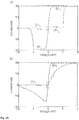
- Figure 2 illustrates simulated current-voltage curves of a quantum-dot memristive system according to the invention derived from a periodic voltage.
- the lever arm of the electrode-L gating QD2 is 1.
- the energy level of QD2 is within the energy gap, i.e. V ⁇ [-1 meV, 1 meV]
- QD2 is empty (
- QD2 is likely empty when the voltage is decreasing but still positive, occupied when the voltage is increasing but still negative and in a mixed state in other cases. Currents are obtained by numerically solving the master equation as described herein.
- the lever arm of the electrode-L gating QD2 is 1.
- Average current through QD1 is obtained by solving the master equation.
- QD2 is likely empty (
- the energy level of QD2 is within the energy gap, i.e. V ⁇ [-0.5 meV, 0.5 meV]
- QD2 is empty (
- Figure 3 illustrates quantum trajectory simulations of the instantaneous current in a quantum-dot memristive system according to the invention. Parameters are the same as described in Example 2.
- Figure 3(a) illustrates the voltage applied on the two terminals as a function of time.
- FIGs 3 (b) and (c) illustrate the current which is produced by the voltage illustrated in (a).
- the energy gap in the electrode-B is open (i.e. non-zero) in (b) and closed (i.e. zero) in (c).
- the instantaneous current (solid curve) is different from the average current (dashed curve) due to quantum jumps, which correspond to sudden changes of the instantaneous current.
- Figure 3(d) shows experimental data which was recorded for a working embodiment (as shown in Figure 1(d) and described in further detail in Example 9).
- the solid curve is the instantaneous current and the dashed curve is the current averaged over 10 sweeps. Arrows indicate the position of abrupt current jumps. The jump positions varied stochastically from sweep to sweep, consistent with the expected behaviour of quantum jumps.
- Figure 4 illustrates quantum trajectory simulations of electron tunnellings in a quantum-dot memristive system according to the invention.
- the energy gap in the electrode-B is open in (a) and (b) and closed in (c) and (d).
- Figures 4(a) and 4(c) illustrate the count of electrons tunnelling from QD1 to electrode-R in a single trial.
- Figures 4(b) and 4(d) illustrate the averaged current obtained from 1000 trials (solid curve) which converges to the dashed curve when the number of trials goes to infinity.
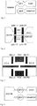
- Figure 5 illustrates a lithographically defined quantum memristive device in which barriers to QD1 and QD2 are formed by lithographically defined notches (constrictions) in the material, which may be a metal or a semiconductor material such as silicon or gallium-arsenide, or a two-dimensional material such as graphene.
- Devices are lithographically defined using electron beam or optical lithography and wet chemical etching, reactive ion etching or plasma etching.
- the QDs are formed between tunnel barriers formed by constrictions (notches) in the channel.
- the devices can be fabricated from metal or semiconductor material such as silicon, or gallium-arsenide, or two-dimensional materials such as graphene.
- Figure 6 illustrates an electrostatically defined quantum memristive device.
- Devices of this type are defined by tunnel barriers which are electrostatically induced by gate electrodes.
- QDs are formed in lithographically defined channels defined by tunnel barriers which are electrostatically induced by gate electrodes.
- Gates L1, L2 and R1, R2 define tunnel-barriers to QD1 and QD2 which are formed in the channel between source and drain/reservoir electrodes.
- the device can be formed in patterned semiconductor materials or semiconductor heterostructures.
- Figure 7 illustrates a further example of an electrostatically defined quantum memristive device.
- Devices of this type are defined by tunnel barriers which are electrostatically induced by gate electrodes.
- QDs are formed in a two-dimensional electron/hole gas.
- Barrier gates BG L1, BG L2, BG R1 and BG R2, and plunger gates PG1 and PG2 define QD1 and QD2 in a two-dimensional electron gas (2DEG).
- Electrode gates EG L and EG R form the barrier between the drain and reservoir electrode.
- the device can be formed in patterned semiconductor materials or semiconductor heterostructures.
- Figure 8 illustrates a quantum memristive device according to the invention in which the QDs are formed by individual atoms, molecules or nanoparticles. Atoms can be placed using ion-implantation or STM lithography. Molecules and nanoparticles can be anchored to the source, drain and reservoir electrode using linker groups.
- FIG. 1(b) Devices according to the invention were fabricated and an example of such a device is shown in Figure 1(b) .
- This device employed a capacitively coupled pair of silicon metal-oxide-semiconductor (MOS) quantum dots.
- MOS silicon metal-oxide-semiconductor
- the two terminals of the memristive system were electrodes L and R, which were formed beneath aluminium accumulation gates LA 1 and LA 2 . These terminals were coupled to the quantum dot QD1 with tunnelling strengths that were determined by the depletion gates LD 1 and RD 1 .
- These devices were fabricated using undoped silicon with a thermal oxide of 300 nm, which was etched down to a thickness of 12 nm in the area where the dots were patterned. Ion implantation of phosphorus with an energy of 12 keV was performed through a photomask to create degenerately doped source/drain contacts. Following implantation, the resist mask was stripped, and the chip was annealed at 950 °C in N 2 to remove damage from the implantation process, and to activate the dopants. To prevent shorts between these ion implanted regions and subsequent metal gates, a 6 nm layer of Al 2 O 3 was deposited by atomic layer deposition. Gates to define the quantum dots were then fabricated on the substrate using three layers of Al gates.
- Each layer was patterned using electron beam lithography with a PMMA mask, and Al deposited using an electron beam evaporator with a deposition rate of 1 ⁇ /s. Following liftoff of the excess metal, the devices were exposed to a 25 W O 2 plasma at 150 °C for two minutes to form an oxide layer at the metal surface. This oxide provided electrical insulation between gate layers, and it was found that this process resulted in gate-gate breakdown voltage greater than 4 V.
- the first gate layer was a screening layer which controlled where subsequent gates would form an accumulation layer at the Si/SiO 2 interface. The screening gates defined two horizontal channels with a separation of -140 nm.
- Layer two were the accumulation gates used to form the conducting channel between the dots and the source/drain contacts, as well as the plunger gates which controlled the chemical potentials of the dots.
- a further layer was deposited last and was used to form tunnel barriers. After all gate layers were deposited, the chip was annealed in forming gas at 220 °C for 1 hour, which was found to be critical for obtaining clean and reproducible device characteristics in this particular embodiment.
- Measurements of device performance were performed. These measurements were carried out in a dilution refrigerator with a lattice temperature of 25 mK. DC voltages were applied to the device using a multi-channel custom voltage source based on the Texas Instruments 1220 20-bit digital to analog converter. To form dots, the screening gates were grounded, a voltage of 2.8 V was applied to the accumulation gates (L/RA 1/2 ), and the plunger gates (P 1/2 ) were set to -2:1 V. For QD1, the depletion gates (L/RD 1 ) were set to -0.8 V to realize relatively low tunnel barriers and a device current on the order of 100 pA.
- the tunnel barriers for QD2 were made larger by applying a voltage of -0.1 V, giving a tunnel rate -10 Hz for QD2 to the left electrode and no tunnelling to the right electrode, as described in the text.
- the plunger gates P 1/2 were then tuned on the mV scale to modulate the chemical potentials of the dots relative to the source and drain electrodes.
- QD1 an attempt was made to align the chemical potential to the electrodes by maximizing the observed DC current at a finite bias.
- a sinusoidal AC voltage with a frequency of 1 Hz was applied to the source of QD1 (L) and one of the depletion gates of QD2 (LD 2 ).
- AC and DC voltages were applied simultaneously to LD2 using a custom-built voltage adder based on an AD797B ultralow-noise operational amplifier.
- the circuit bandwidth was ⁇ 2 Hz due to RC filters on the lines connecting the external sources to the device, which limited the frequency of the applied voltage to ⁇ 2 Hz.
- the 10 mV AC signal was applied directly to LD 2 , but reduced by a factor of 10 using a voltage divider before being applied to L.
- the current through QD1 was amplified using a DL Instruments 1211 current-voltage preamplifier and then input to a Tektronix DPO 7104 oscilloscope. The oscilloscope recorded traces of length 10 s, with a sampling rate of 1 kS/s.
- Figure 9 shows simulated and experimental I-V curves showing current hysteresis in this Si double dot system.
- 1 ⁇ 2 indicate the charge state of QD2.
- Fig 9(b) shows the measured two-looped hysteresis showing similar behavior as in Fig 9(a).
- Fig 9(c) shows that the position of the hysteresis was shifted to negative bias by lowering V P2 which changed the energy level E 2 in QD2.
- _ ⁇ V P2 denotes the difference in voltage applied to V P2 , relative to when the hysteresis was symmetric about zero bias.
- Fig 9(d) shows that raising the DC voltage on LD 2 lowered the tunnel barrier and increased ⁇ 2 , causing the hysteresis width to narrow.
- the estimated tunnel rates ⁇ 2 for Figs 9(c) and 9(d) were 8 Hz and 33 Hz, respectively.
- Figure 9 shows the I-V responses for a single voltage cycle (in contrast to the average current presented in Fig.2 that would correspond to an average over many cycles).
- Fig. 9(a) is a simulated trace using Equations (7) and (8) with instantaneous switching of the charge state of QD2 chosen to match the data in Figure 9(b) .
- Tuning the DC voltages applied to QD2 varied the hysteresis shape in two distinct ways.
- the plunger gate P 2 controlled the value of E 2 .
- the position of the hysteresis loop was thus shifted along the I-V curve, as shown in Figure 9(c) . This confirmed that the current jumps in the current of QD1 were due to charge transitions on QD2. If QD2 is detuned far enough, the voltage V would no longer be sufficient to cause the dot level to cross ⁇ B and no hysteresis would be observed.
- Comparison of Figures 9(a) and 9(b) showed that this model reproduced the experimental data well. If the effect of the tunnel barrier resistance is removed and the I-V response of the double dot system is plotted instead, a curve similar to Figure 2B(a) was obtained, but with stochastic jumps rather than an average current.
- the tunnelling rate ⁇ 2 must be in the correct frequency range in order to observe the memristive hysteresis effect, i.e. roughly comparable to sweep rate ⁇ .
- the width of the hysteresis loop was modulated by adjusting ⁇ 2 , using the DC voltage on the depletion gate LD 2 . This can be seen in Figures 9(c) and 9(d) , where a more positive voltage in (d) increased the tunnelling rate and the charge transitions occurred closer together. If the tunnel rate were further increased the hysteresis would eventually disappear.
- tunnelling rates 8 Hz and 33 Hz were estimated, respectively.
Landscapes
- Engineering & Computer Science (AREA)
- Chemical & Material Sciences (AREA)
- Materials Engineering (AREA)
- Manufacturing & Machinery (AREA)
- Semiconductor Memories (AREA)
- Thin Film Transistor (AREA)
- Superconductor Devices And Manufacturing Methods Thereof (AREA)
Claims (15)
- Quantenmemristor, umfassend:einen ersten Quantenpunkt QD1, der kapazitiv an einen zweiten Quantenpunkt QD2 gekoppelt ist,eine Source-Elektrode,eine Drain-Elektrode undeine Bad-Elektrode,wobei die Source-Elektrode und die Drain-Elektrode über Quantentunnelung an QD1 und die Bad-Elektrode über Quantentunnelung an QD2 gekoppelt sind, und wobei QD2 kapazitiv entweder an die Source-Elektrode oder an die Drain-Elektrode gekoppelt ist.
- Quantenmemristor nach Anspruch 1, wobei QD1 und QD2 aus dem gleichen Material bestehen.
- Quantenmemristor nach Anspruch 1, wobei QD1 und QD2 aus voneinander unterschiedlichen Materialien bestehen.
- Quantenmemristor nach einem der Ansprüche 1 bis 3, wobei QD1 und QD2 die gleiche Größe und/oder Form haben.
- Quantenmemristor nach einem der Ansprüche 1 bis 4, wobei QD1, die Source-Elektrode und die Drain-Elektrode aus einem einzigen Materialstück gebildet sind und wobei QD1 durch eine erste Einschnürung und eine zweite Einschnürung in dem einzigen Materialstück definiert ist, wobei die erste Einschnürung zwischen QD1 und der Source-Elektrode und die zweite Einschnürung zwischen QD1 und der Drain-Elektrode angeordnet ist; und wobei QD2 und die Bad-Elektrode aus einem einzigen Materialstück gebildet sind und wobei QD2 durch eine Einschnürung in dem einzigen Materialstück definiert ist, die sich zwischen QD2 und der Bad-Elektrode befindet; wobei die Einschnürungen zwischen QD1 und der Source- und Drain-Elektrode und zwischen QD2 und der Bad-Elektrode als Tunnelbarrieren wirken; und optional, wobei diese Einschnürungen lithographisch hergestellt werden.
- Quantenmemristor nach einem der Ansprüche 1 bis 4, wobei sich QD1 und QD2 in lithographisch definierten Kanälen befinden und wobei Tunnelbarrieren zwischen QD1, der Source-Elektrode und der Drain-Elektrode sowie zwischen QD2 und der Bad-Elektrode durch Gate-Elektroden bereitgestellt werden.
- Quantenmemristor nach einem der Ansprüche 1 bis 4, wobei QD1 und QD2 Bereiche in einem zweidimensionalen Elektronen-/Löchergas sind, die durch Barriere-Gates und Plunger-Gates definiert sind; optional, wobei das zweidimensionale Elektronen-/Löchergas ein strukturiertes Halbleitermaterial ist; optional, wobei das Halbleitermaterial eine Halbleiter-Heterostruktur ist; und wobei QD1 durch Elektroden-Gates von der Drain- und Reservoir-Elektrode getrennt ist.
- Quantenmemristor nach einem der Ansprüche 1 bis 4, wobei QD1 und QD2 jeweils unabhängig voneinander ein einzelnes Atom, Molekül oder Nanopartikel sind.
- Quantenmemristor nach einem der vorstehenden Ansprüche, wobei die Bad-Elektrode eine Energielücke ungleich Null aufweist.
- Mehrfach-Quantenpunkt-Memristor umfassend zwei oder mehr Quantenmemristoren, wie in einem der Ansprüche 1 bis 9 definiert, wobei die zwei oder mehr Quantenmemristoren parallel angeordnet sind.
- Computerlesbares Speichermedium umfassend mindestens einem Quantenmemristor nach einem der Ansprüche 1 bis 9 oder mindestens einem Mehrfach-Quantenpunkt-Memristor nach Anspruch 10.
- Verfahren zur Speicherung von Informationen in einem Quantenmemristor, wobei das Verfahren umfasst:Bereitstellen eines Quantenmemristors, wie in einem der Ansprüche 1 bis 9 definiert, wobei QD2 einen ersten Belegungsgrad aufweist;und Anlegen einer Spannung zwischen der ersten und der zweiten Elektrode, um die Belegungsebene von QD2 auf eine zweite Belegungsebene zu ändern;wobei das Ändern der Belegungsebene von QD2 von der ersten auf die zweite Belegungsebene der Speicherung von mindestens einem Informationsbit entspricht.
- Verfahren nach Anspruch 12, wobei die Information eine binäre Information ist; und optional wobei eine der ersten und zweiten Belegungsebenen von QD2 einer 1 in binärer Sprache entspricht und die andere der ersten und zweiten Belegungsebenen von QD2 einer 0 in binärer Sprache entspricht.
- Verfahren nach Anspruch 12, wobei die Information eine Quanteninformation ist; optional wobei das Ändern der Belegungsebene von QD2 von der ersten auf die zweite Belegungsebene der Speicherung von mindestens einem Qubit entspricht.
- Verfahren nach Anspruch 12, wobei die Speicherung von Informationen in einem Computersystem erfolgt; wobei das Computersystem einen Quantencomputer umfasst.
Applications Claiming Priority (2)
| Application Number | Priority Date | Filing Date | Title |
|---|---|---|---|
| GB201607062 | 2016-04-22 | ||
| PCT/GB2017/051122 WO2017182826A1 (en) | 2016-04-22 | 2017-04-21 | Coupled quantum dot memristor |
Publications (2)
| Publication Number | Publication Date |
|---|---|
| EP3446342A1 EP3446342A1 (de) | 2019-02-27 |
| EP3446342B1 true EP3446342B1 (de) | 2020-03-25 |
Family
ID=58638889
Family Applications (1)
| Application Number | Title | Priority Date | Filing Date |
|---|---|---|---|
| EP17719893.4A Active EP3446342B1 (de) | 2016-04-22 | 2017-04-21 | Gekoppelter quanten-dot-memristor |
Country Status (3)
| Country | Link |
|---|---|
| US (1) | US10510956B2 (de) |
| EP (1) | EP3446342B1 (de) |
| WO (1) | WO2017182826A1 (de) |
Families Citing this family (7)
| Publication number | Priority date | Publication date | Assignee | Title |
|---|---|---|---|---|
| US10817780B2 (en) * | 2017-10-29 | 2020-10-27 | Christopher J. Rourk | Electron transport gate circuits and methods of manufacture, operation and use |
| US10490727B2 (en) * | 2018-02-20 | 2019-11-26 | Intel Corporation | Gate arrangements in quantum dot devices |
| US10475912B2 (en) * | 2018-02-20 | 2019-11-12 | Intel Corporation | Gate arrangements in quantum dot devices |
| CN111276561B (zh) * | 2020-02-17 | 2023-05-02 | 电子科技大学 | 一种基于范德华异质结的非易失光存储单元及其制备方法 |
| EP4086821A1 (de) * | 2021-05-07 | 2022-11-09 | Universität Wien | Quantenoptischer memristor |
| US20230389346A1 (en) * | 2022-05-24 | 2023-11-30 | National Yang Ming Chiao Tung University | Quantum devices and methods for making the same |
| JP2024040790A (ja) | 2022-09-13 | 2024-03-26 | 学校法人帝京大学 | 半導体量子装置 |
Family Cites Families (8)
| Publication number | Priority date | Publication date | Assignee | Title |
|---|---|---|---|---|
| JP4873335B2 (ja) | 2000-04-28 | 2012-02-08 | 独立行政法人科学技術振興機構 | 情報処理構造体 |
| EP1262911A1 (de) * | 2001-05-30 | 2002-12-04 | Hitachi Europe Limited | Quantenrechner |
| US6844566B2 (en) | 2003-05-30 | 2005-01-18 | Texas Instruments Incorporated | Suspended gate single-electron device |
| EP2309562B1 (de) * | 2009-10-12 | 2012-12-05 | Hitachi Ltd. | Ladungsträgervorrichtung |
| US8050078B2 (en) | 2009-10-27 | 2011-11-01 | Hewlett-Packard Development Company, L.P. | Nanowire-based memristor devices |
| KR101537433B1 (ko) | 2011-08-24 | 2015-07-17 | 한양대학교 산학협력단 | 멤리스터 소자 및 이의 제조방법 |
| EP2751807A4 (de) | 2011-09-02 | 2015-02-18 | Hewlett Packard Development Co | Vorrichtung zur speicherung von daten und verfahren zum lesen von speicherzellen |
| US9035272B2 (en) * | 2013-01-16 | 2015-05-19 | Hewlett-Packard Development Company, L.P. | Nanoparticle-based memristor structure |
-
2017
- 2017-04-21 EP EP17719893.4A patent/EP3446342B1/de active Active
- 2017-04-21 US US16/095,150 patent/US10510956B2/en not_active Expired - Fee Related
- 2017-04-21 WO PCT/GB2017/051122 patent/WO2017182826A1/en not_active Ceased
Non-Patent Citations (1)
| Title |
|---|
| None * |
Also Published As
| Publication number | Publication date |
|---|---|
| US20190058117A1 (en) | 2019-02-21 |
| WO2017182826A1 (en) | 2017-10-26 |
| US10510956B2 (en) | 2019-12-17 |
| EP3446342A1 (de) | 2019-02-27 |
Similar Documents
| Publication | Publication Date | Title |
|---|---|---|
| US10510956B2 (en) | Coupled quantum dot memristor | |
| Shin et al. | Multilevel resistive switching nonvolatile memory based on MoS2 nanosheet-embedded graphene oxide | |
| Mehrez et al. | I− V characteristics and differential conductance fluctuations of Au nanowires | |
| Svizhenko et al. | Effect of growth orientation and surface roughness on electron transport in silicon nanowires | |
| Ermakov et al. | Phenomena in resonant tunneling through degenerated energy states with electron correlation | |
| Li et al. | Double quantum dot memristor | |
| Harry et al. | Confinement energy of quantum dots and the brus equation | |
| KR20190031513A (ko) | 다수의 규소 원자 양자점 및 이를 포함하는 디바이스 | |
| WO2021191629A1 (en) | Fabrication method of a nanodevice with a nanogap electrode | |
| Sakai et al. | Fabrication of atomic junctions with experimental parameters optimized using ground-state searches of Ising spin computing | |
| Mendez | Physics of resonant tunneling in semiconductors | |
| Salfi et al. | Evidence for nonlinear screening and enhancement of scattering by a single Coulomb impurity for dielectrically confined electrons in InAs nanowires | |
| Beecher et al. | Charge transport in weakly coupled CoPt3 nanocrystal assemblies | |
| Balaguru et al. | Quantum size effect, electrical conductivity and quantum transport | |
| Knobloch et al. | Impact of gate dielectrics on the threshold voltage in MoS2 transistors | |
| Quinn et al. | Artificial atom solids based on metal nanocrystals: Formation and electrical properties | |
| US20160064249A1 (en) | Local doping of two-dimensional materials | |
| Mirdha et al. | An investigation of quantum dot super lattice use in Nonvolatile Memory and Transistors | |
| Bellucci et al. | Transport through a double barrier for interacting quasi one-dimensional electrons in a quantum wire in the presence of a transverse magnetic field | |
| Cervera et al. | Information processing schemes based on monolayer protected metallic nanoclusters | |
| Nikolić | Electronic transport in nanoparticle arrays: The effect of structural disorder | |
| Schöll et al. | Nonlinear and oscillatory electronic transport in superlattices as a probe of structural imperfections | |
| Ishibashi et al. | Low-temperature transport in single and coupled quantum dots in single-wall carbon nanotubes | |
| Mittag | Electronic Transport in InAs Quantum Devices | |
| Wong et al. | Local doping of two-dimensional materials |
Legal Events
| Date | Code | Title | Description |
|---|---|---|---|
| STAA | Information on the status of an ep patent application or granted ep patent |
Free format text: STATUS: UNKNOWN |
|
| STAA | Information on the status of an ep patent application or granted ep patent |
Free format text: STATUS: THE INTERNATIONAL PUBLICATION HAS BEEN MADE |
|
| PUAI | Public reference made under article 153(3) epc to a published international application that has entered the european phase |
Free format text: ORIGINAL CODE: 0009012 |
|
| STAA | Information on the status of an ep patent application or granted ep patent |
Free format text: STATUS: REQUEST FOR EXAMINATION WAS MADE |
|
| 17P | Request for examination filed |
Effective date: 20181119 |
|
| AK | Designated contracting states |
Kind code of ref document: A1 Designated state(s): AL AT BE BG CH CY CZ DE DK EE ES FI FR GB GR HR HU IE IS IT LI LT LU LV MC MK MT NL NO PL PT RO RS SE SI SK SM TR |
|
| AX | Request for extension of the european patent |
Extension state: BA ME |
|
| DAV | Request for validation of the european patent (deleted) | ||
| DAX | Request for extension of the european patent (deleted) | ||
| GRAP | Despatch of communication of intention to grant a patent |
Free format text: ORIGINAL CODE: EPIDOSNIGR1 |
|
| STAA | Information on the status of an ep patent application or granted ep patent |
Free format text: STATUS: GRANT OF PATENT IS INTENDED |
|
| INTG | Intention to grant announced |
Effective date: 20191002 |
|
| GRAS | Grant fee paid |
Free format text: ORIGINAL CODE: EPIDOSNIGR3 |
|
| GRAA | (expected) grant |
Free format text: ORIGINAL CODE: 0009210 |
|
| STAA | Information on the status of an ep patent application or granted ep patent |
Free format text: STATUS: THE PATENT HAS BEEN GRANTED |
|
| AK | Designated contracting states |
Kind code of ref document: B1 Designated state(s): AL AT BE BG CH CY CZ DE DK EE ES FI FR GB GR HR HU IE IS IT LI LT LU LV MC MK MT NL NO PL PT RO RS SE SI SK SM TR |
|
| REG | Reference to a national code |
Ref country code: GB Ref legal event code: FG4D |
|
| REG | Reference to a national code |
Ref country code: AT Ref legal event code: REF Ref document number: 1249604 Country of ref document: AT Kind code of ref document: T Effective date: 20200415 Ref country code: IE Ref legal event code: FG4D |
|
| REG | Reference to a national code |
Ref country code: DE Ref legal event code: R096 Ref document number: 602017013648 Country of ref document: DE |
|
| PG25 | Lapsed in a contracting state [announced via postgrant information from national office to epo] |
Ref country code: FI Free format text: LAPSE BECAUSE OF FAILURE TO SUBMIT A TRANSLATION OF THE DESCRIPTION OR TO PAY THE FEE WITHIN THE PRESCRIBED TIME-LIMIT Effective date: 20200325 Ref country code: NO Free format text: LAPSE BECAUSE OF FAILURE TO SUBMIT A TRANSLATION OF THE DESCRIPTION OR TO PAY THE FEE WITHIN THE PRESCRIBED TIME-LIMIT Effective date: 20200625 Ref country code: RS Free format text: LAPSE BECAUSE OF FAILURE TO SUBMIT A TRANSLATION OF THE DESCRIPTION OR TO PAY THE FEE WITHIN THE PRESCRIBED TIME-LIMIT Effective date: 20200325 |
|
| PG25 | Lapsed in a contracting state [announced via postgrant information from national office to epo] |
Ref country code: GR Free format text: LAPSE BECAUSE OF FAILURE TO SUBMIT A TRANSLATION OF THE DESCRIPTION OR TO PAY THE FEE WITHIN THE PRESCRIBED TIME-LIMIT Effective date: 20200626 Ref country code: BG Free format text: LAPSE BECAUSE OF FAILURE TO SUBMIT A TRANSLATION OF THE DESCRIPTION OR TO PAY THE FEE WITHIN THE PRESCRIBED TIME-LIMIT Effective date: 20200625 Ref country code: HR Free format text: LAPSE BECAUSE OF FAILURE TO SUBMIT A TRANSLATION OF THE DESCRIPTION OR TO PAY THE FEE WITHIN THE PRESCRIBED TIME-LIMIT Effective date: 20200325 Ref country code: SE Free format text: LAPSE BECAUSE OF FAILURE TO SUBMIT A TRANSLATION OF THE DESCRIPTION OR TO PAY THE FEE WITHIN THE PRESCRIBED TIME-LIMIT Effective date: 20200325 Ref country code: LV Free format text: LAPSE BECAUSE OF FAILURE TO SUBMIT A TRANSLATION OF THE DESCRIPTION OR TO PAY THE FEE WITHIN THE PRESCRIBED TIME-LIMIT Effective date: 20200325 |
|
| REG | Reference to a national code |
Ref country code: NL Ref legal event code: MP Effective date: 20200325 |
|
| REG | Reference to a national code |
Ref country code: LT Ref legal event code: MG4D |
|
| PG25 | Lapsed in a contracting state [announced via postgrant information from national office to epo] |
Ref country code: NL Free format text: LAPSE BECAUSE OF FAILURE TO SUBMIT A TRANSLATION OF THE DESCRIPTION OR TO PAY THE FEE WITHIN THE PRESCRIBED TIME-LIMIT Effective date: 20200325 |
|
| PG25 | Lapsed in a contracting state [announced via postgrant information from national office to epo] |
Ref country code: CZ Free format text: LAPSE BECAUSE OF FAILURE TO SUBMIT A TRANSLATION OF THE DESCRIPTION OR TO PAY THE FEE WITHIN THE PRESCRIBED TIME-LIMIT Effective date: 20200325 Ref country code: IS Free format text: LAPSE BECAUSE OF FAILURE TO SUBMIT A TRANSLATION OF THE DESCRIPTION OR TO PAY THE FEE WITHIN THE PRESCRIBED TIME-LIMIT Effective date: 20200725 Ref country code: SK Free format text: LAPSE BECAUSE OF FAILURE TO SUBMIT A TRANSLATION OF THE DESCRIPTION OR TO PAY THE FEE WITHIN THE PRESCRIBED TIME-LIMIT Effective date: 20200325 Ref country code: PT Free format text: LAPSE BECAUSE OF FAILURE TO SUBMIT A TRANSLATION OF THE DESCRIPTION OR TO PAY THE FEE WITHIN THE PRESCRIBED TIME-LIMIT Effective date: 20200818 Ref country code: SM Free format text: LAPSE BECAUSE OF FAILURE TO SUBMIT A TRANSLATION OF THE DESCRIPTION OR TO PAY THE FEE WITHIN THE PRESCRIBED TIME-LIMIT Effective date: 20200325 Ref country code: LT Free format text: LAPSE BECAUSE OF FAILURE TO SUBMIT A TRANSLATION OF THE DESCRIPTION OR TO PAY THE FEE WITHIN THE PRESCRIBED TIME-LIMIT Effective date: 20200325 Ref country code: RO Free format text: LAPSE BECAUSE OF FAILURE TO SUBMIT A TRANSLATION OF THE DESCRIPTION OR TO PAY THE FEE WITHIN THE PRESCRIBED TIME-LIMIT Effective date: 20200325 Ref country code: EE Free format text: LAPSE BECAUSE OF FAILURE TO SUBMIT A TRANSLATION OF THE DESCRIPTION OR TO PAY THE FEE WITHIN THE PRESCRIBED TIME-LIMIT Effective date: 20200325 |
|
| REG | Reference to a national code |
Ref country code: AT Ref legal event code: MK05 Ref document number: 1249604 Country of ref document: AT Kind code of ref document: T Effective date: 20200325 |
|
| REG | Reference to a national code |
Ref country code: CH Ref legal event code: PL |
|
| PG25 | Lapsed in a contracting state [announced via postgrant information from national office to epo] |
Ref country code: MC Free format text: LAPSE BECAUSE OF FAILURE TO SUBMIT A TRANSLATION OF THE DESCRIPTION OR TO PAY THE FEE WITHIN THE PRESCRIBED TIME-LIMIT Effective date: 20200325 |
|
| REG | Reference to a national code |
Ref country code: DE Ref legal event code: R097 Ref document number: 602017013648 Country of ref document: DE |
|
| PG25 | Lapsed in a contracting state [announced via postgrant information from national office to epo] |
Ref country code: DK Free format text: LAPSE BECAUSE OF FAILURE TO SUBMIT A TRANSLATION OF THE DESCRIPTION OR TO PAY THE FEE WITHIN THE PRESCRIBED TIME-LIMIT Effective date: 20200325 Ref country code: LU Free format text: LAPSE BECAUSE OF NON-PAYMENT OF DUE FEES Effective date: 20200421 Ref country code: ES Free format text: LAPSE BECAUSE OF FAILURE TO SUBMIT A TRANSLATION OF THE DESCRIPTION OR TO PAY THE FEE WITHIN THE PRESCRIBED TIME-LIMIT Effective date: 20200325 Ref country code: CH Free format text: LAPSE BECAUSE OF NON-PAYMENT OF DUE FEES Effective date: 20200430 Ref country code: IT Free format text: LAPSE BECAUSE OF FAILURE TO SUBMIT A TRANSLATION OF THE DESCRIPTION OR TO PAY THE FEE WITHIN THE PRESCRIBED TIME-LIMIT Effective date: 20200325 Ref country code: AT Free format text: LAPSE BECAUSE OF FAILURE TO SUBMIT A TRANSLATION OF THE DESCRIPTION OR TO PAY THE FEE WITHIN THE PRESCRIBED TIME-LIMIT Effective date: 20200325 Ref country code: LI Free format text: LAPSE BECAUSE OF NON-PAYMENT OF DUE FEES Effective date: 20200430 |
|
| REG | Reference to a national code |
Ref country code: BE Ref legal event code: MM Effective date: 20200430 |
|
| PLBE | No opposition filed within time limit |
Free format text: ORIGINAL CODE: 0009261 |
|
| STAA | Information on the status of an ep patent application or granted ep patent |
Free format text: STATUS: NO OPPOSITION FILED WITHIN TIME LIMIT |
|
| PG25 | Lapsed in a contracting state [announced via postgrant information from national office to epo] |
Ref country code: PL Free format text: LAPSE BECAUSE OF FAILURE TO SUBMIT A TRANSLATION OF THE DESCRIPTION OR TO PAY THE FEE WITHIN THE PRESCRIBED TIME-LIMIT Effective date: 20200325 Ref country code: BE Free format text: LAPSE BECAUSE OF NON-PAYMENT OF DUE FEES Effective date: 20200430 |
|
| 26N | No opposition filed |
Effective date: 20210112 |
|
| PG25 | Lapsed in a contracting state [announced via postgrant information from national office to epo] |
Ref country code: IE Free format text: LAPSE BECAUSE OF NON-PAYMENT OF DUE FEES Effective date: 20200421 |
|
| PG25 | Lapsed in a contracting state [announced via postgrant information from national office to epo] |
Ref country code: SI Free format text: LAPSE BECAUSE OF FAILURE TO SUBMIT A TRANSLATION OF THE DESCRIPTION OR TO PAY THE FEE WITHIN THE PRESCRIBED TIME-LIMIT Effective date: 20200325 |
|
| PG25 | Lapsed in a contracting state [announced via postgrant information from national office to epo] |
Ref country code: TR Free format text: LAPSE BECAUSE OF FAILURE TO SUBMIT A TRANSLATION OF THE DESCRIPTION OR TO PAY THE FEE WITHIN THE PRESCRIBED TIME-LIMIT Effective date: 20200325 Ref country code: MT Free format text: LAPSE BECAUSE OF FAILURE TO SUBMIT A TRANSLATION OF THE DESCRIPTION OR TO PAY THE FEE WITHIN THE PRESCRIBED TIME-LIMIT Effective date: 20200325 Ref country code: CY Free format text: LAPSE BECAUSE OF FAILURE TO SUBMIT A TRANSLATION OF THE DESCRIPTION OR TO PAY THE FEE WITHIN THE PRESCRIBED TIME-LIMIT Effective date: 20200325 |
|
| PG25 | Lapsed in a contracting state [announced via postgrant information from national office to epo] |
Ref country code: MK Free format text: LAPSE BECAUSE OF FAILURE TO SUBMIT A TRANSLATION OF THE DESCRIPTION OR TO PAY THE FEE WITHIN THE PRESCRIBED TIME-LIMIT Effective date: 20200325 Ref country code: AL Free format text: LAPSE BECAUSE OF FAILURE TO SUBMIT A TRANSLATION OF THE DESCRIPTION OR TO PAY THE FEE WITHIN THE PRESCRIBED TIME-LIMIT Effective date: 20200325 |
|
| REG | Reference to a national code |
Ref country code: DE Ref legal event code: R079 Ref document number: 602017013648 Country of ref document: DE Free format text: PREVIOUS MAIN CLASS: H01L0045000000 Ipc: H10N0070000000 |
|
| P01 | Opt-out of the competence of the unified patent court (upc) registered |
Effective date: 20230526 |
|
| PGFP | Annual fee paid to national office [announced via postgrant information from national office to epo] |
Ref country code: DE Payment date: 20250417 Year of fee payment: 9 |
|
| PGFP | Annual fee paid to national office [announced via postgrant information from national office to epo] |
Ref country code: GB Payment date: 20250415 Year of fee payment: 9 |
|
| PGFP | Annual fee paid to national office [announced via postgrant information from national office to epo] |
Ref country code: FR Payment date: 20250422 Year of fee payment: 9 |