EP3446331B1 - Wirelessly powered high security document with visual indicator - Google Patents
Wirelessly powered high security document with visual indicator Download PDFInfo
- Publication number
- EP3446331B1 EP3446331B1 EP17723274.1A EP17723274A EP3446331B1 EP 3446331 B1 EP3446331 B1 EP 3446331B1 EP 17723274 A EP17723274 A EP 17723274A EP 3446331 B1 EP3446331 B1 EP 3446331B1
- Authority
- EP
- European Patent Office
- Prior art keywords
- light
- antenna
- electronic circuit
- security document
- micro
- Prior art date
- Legal status (The legal status is an assumption and is not a legal conclusion. Google has not performed a legal analysis and makes no representation as to the accuracy of the status listed.)
- Active
Links
Images


Classifications
-
- G—PHYSICS
- G09—EDUCATION; CRYPTOGRAPHY; DISPLAY; ADVERTISING; SEALS
- G09G—ARRANGEMENTS OR CIRCUITS FOR CONTROL OF INDICATING DEVICES USING STATIC MEANS TO PRESENT VARIABLE INFORMATION
- G09G3/00—Control arrangements or circuits, of interest only in connection with visual indicators other than cathode-ray tubes
- G09G3/20—Control arrangements or circuits, of interest only in connection with visual indicators other than cathode-ray tubes for presentation of an assembly of a number of characters, e.g. a page, by composing the assembly by combination of individual elements arranged in a matrix no fixed position being assigned to or needed to be assigned to the individual characters or partial characters
- G09G3/22—Control arrangements or circuits, of interest only in connection with visual indicators other than cathode-ray tubes for presentation of an assembly of a number of characters, e.g. a page, by composing the assembly by combination of individual elements arranged in a matrix no fixed position being assigned to or needed to be assigned to the individual characters or partial characters using controlled light sources
- G09G3/30—Control arrangements or circuits, of interest only in connection with visual indicators other than cathode-ray tubes for presentation of an assembly of a number of characters, e.g. a page, by composing the assembly by combination of individual elements arranged in a matrix no fixed position being assigned to or needed to be assigned to the individual characters or partial characters using controlled light sources using electroluminescent panels
- G09G3/32—Control arrangements or circuits, of interest only in connection with visual indicators other than cathode-ray tubes for presentation of an assembly of a number of characters, e.g. a page, by composing the assembly by combination of individual elements arranged in a matrix no fixed position being assigned to or needed to be assigned to the individual characters or partial characters using controlled light sources using electroluminescent panels semiconductive, e.g. using light-emitting diodes [LED]
-
- G—PHYSICS
- G06—COMPUTING OR CALCULATING; COUNTING
- G06K—GRAPHICAL DATA READING; PRESENTATION OF DATA; RECORD CARRIERS; HANDLING RECORD CARRIERS
- G06K19/00—Record carriers for use with machines and with at least a part designed to carry digital markings
- G06K19/06—Record carriers for use with machines and with at least a part designed to carry digital markings characterised by the kind of the digital marking, e.g. shape, nature, code
- G06K19/067—Record carriers with conductive marks, printed circuits or semiconductor circuit elements, e.g. credit or identity cards also with resonating or responding marks without active components
- G06K19/07—Record carriers with conductive marks, printed circuits or semiconductor circuit elements, e.g. credit or identity cards also with resonating or responding marks without active components with integrated circuit chips
- G06K19/0701—Record carriers with conductive marks, printed circuits or semiconductor circuit elements, e.g. credit or identity cards also with resonating or responding marks without active components with integrated circuit chips at least one of the integrated circuit chips comprising an arrangement for power management
- G06K19/0707—Record carriers with conductive marks, printed circuits or semiconductor circuit elements, e.g. credit or identity cards also with resonating or responding marks without active components with integrated circuit chips at least one of the integrated circuit chips comprising an arrangement for power management the arrangement being capable of collecting energy from external energy sources, e.g. thermocouples, vibration, electromagnetic radiation
- G06K19/0708—Record carriers with conductive marks, printed circuits or semiconductor circuit elements, e.g. credit or identity cards also with resonating or responding marks without active components with integrated circuit chips at least one of the integrated circuit chips comprising an arrangement for power management the arrangement being capable of collecting energy from external energy sources, e.g. thermocouples, vibration, electromagnetic radiation the source being electromagnetic or magnetic
- G06K19/071—Record carriers with conductive marks, printed circuits or semiconductor circuit elements, e.g. credit or identity cards also with resonating or responding marks without active components with integrated circuit chips at least one of the integrated circuit chips comprising an arrangement for power management the arrangement being capable of collecting energy from external energy sources, e.g. thermocouples, vibration, electromagnetic radiation the source being electromagnetic or magnetic the source being a field other than an interrogation field, e.g. WLAN, cellular phone network
-
- G—PHYSICS
- G06—COMPUTING OR CALCULATING; COUNTING
- G06K—GRAPHICAL DATA READING; PRESENTATION OF DATA; RECORD CARRIERS; HANDLING RECORD CARRIERS
- G06K19/00—Record carriers for use with machines and with at least a part designed to carry digital markings
- G06K19/06—Record carriers for use with machines and with at least a part designed to carry digital markings characterised by the kind of the digital marking, e.g. shape, nature, code
- G06K19/067—Record carriers with conductive marks, printed circuits or semiconductor circuit elements, e.g. credit or identity cards also with resonating or responding marks without active components
- G06K19/07—Record carriers with conductive marks, printed circuits or semiconductor circuit elements, e.g. credit or identity cards also with resonating or responding marks without active components with integrated circuit chips
- G06K19/0723—Record carriers with conductive marks, printed circuits or semiconductor circuit elements, e.g. credit or identity cards also with resonating or responding marks without active components with integrated circuit chips the record carrier comprising an arrangement for non-contact communication, e.g. wireless communication circuits on transponder cards, non-contact smart cards or RFIDs
-
- G—PHYSICS
- G06—COMPUTING OR CALCULATING; COUNTING
- G06K—GRAPHICAL DATA READING; PRESENTATION OF DATA; RECORD CARRIERS; HANDLING RECORD CARRIERS
- G06K19/00—Record carriers for use with machines and with at least a part designed to carry digital markings
- G06K19/06—Record carriers for use with machines and with at least a part designed to carry digital markings characterised by the kind of the digital marking, e.g. shape, nature, code
- G06K19/067—Record carriers with conductive marks, printed circuits or semiconductor circuit elements, e.g. credit or identity cards also with resonating or responding marks without active components
- G06K19/07—Record carriers with conductive marks, printed circuits or semiconductor circuit elements, e.g. credit or identity cards also with resonating or responding marks without active components with integrated circuit chips
- G06K19/077—Constructional details, e.g. mounting of circuits in the carrier
- G06K19/07701—Constructional details, e.g. mounting of circuits in the carrier the record carrier comprising an interface suitable for human interaction
- G06K19/07703—Constructional details, e.g. mounting of circuits in the carrier the record carrier comprising an interface suitable for human interaction the interface being visual
- G06K19/07705—Constructional details, e.g. mounting of circuits in the carrier the record carrier comprising an interface suitable for human interaction the interface being visual the visual interface being a single light or small number of lights capable of being switched on or off, e.g. a series of LEDs
-
- G—PHYSICS
- G06—COMPUTING OR CALCULATING; COUNTING
- G06K—GRAPHICAL DATA READING; PRESENTATION OF DATA; RECORD CARRIERS; HANDLING RECORD CARRIERS
- G06K19/00—Record carriers for use with machines and with at least a part designed to carry digital markings
- G06K19/06—Record carriers for use with machines and with at least a part designed to carry digital markings characterised by the kind of the digital marking, e.g. shape, nature, code
- G06K19/067—Record carriers with conductive marks, printed circuits or semiconductor circuit elements, e.g. credit or identity cards also with resonating or responding marks without active components
- G06K19/07—Record carriers with conductive marks, printed circuits or semiconductor circuit elements, e.g. credit or identity cards also with resonating or responding marks without active components with integrated circuit chips
- G06K19/077—Constructional details, e.g. mounting of circuits in the carrier
- G06K19/07749—Constructional details, e.g. mounting of circuits in the carrier the record carrier being capable of non-contact communication, e.g. constructional details of the antenna of a non-contact smart card
-
- G—PHYSICS
- G07—CHECKING-DEVICES
- G07D—HANDLING OF COINS OR VALUABLE PAPERS, e.g. TESTING, SORTING BY DENOMINATIONS, COUNTING, DISPENSING, CHANGING OR DEPOSITING
- G07D7/00—Testing specially adapted to determine the identity or genuineness of valuable papers or for segregating those which are unacceptable, e.g. banknotes that are alien to a currency
- G07D7/004—Testing specially adapted to determine the identity or genuineness of valuable papers or for segregating those which are unacceptable, e.g. banknotes that are alien to a currency using digital security elements, e.g. information coded on a magnetic thread or strip
-
- G—PHYSICS
- G07—CHECKING-DEVICES
- G07D—HANDLING OF COINS OR VALUABLE PAPERS, e.g. TESTING, SORTING BY DENOMINATIONS, COUNTING, DISPENSING, CHANGING OR DEPOSITING
- G07D7/00—Testing specially adapted to determine the identity or genuineness of valuable papers or for segregating those which are unacceptable, e.g. banknotes that are alien to a currency
- G07D7/01—Testing electronic circuits therein
-
- G—PHYSICS
- G07—CHECKING-DEVICES
- G07D—HANDLING OF COINS OR VALUABLE PAPERS, e.g. TESTING, SORTING BY DENOMINATIONS, COUNTING, DISPENSING, CHANGING OR DEPOSITING
- G07D7/00—Testing specially adapted to determine the identity or genuineness of valuable papers or for segregating those which are unacceptable, e.g. banknotes that are alien to a currency
- G07D7/06—Testing specially adapted to determine the identity or genuineness of valuable papers or for segregating those which are unacceptable, e.g. banknotes that are alien to a currency using wave or particle radiation
- G07D7/12—Visible light, infrared or ultraviolet radiation
- G07D7/1205—Testing spectral properties
-
- G—PHYSICS
- G07—CHECKING-DEVICES
- G07D—HANDLING OF COINS OR VALUABLE PAPERS, e.g. TESTING, SORTING BY DENOMINATIONS, COUNTING, DISPENSING, CHANGING OR DEPOSITING
- G07D7/00—Testing specially adapted to determine the identity or genuineness of valuable papers or for segregating those which are unacceptable, e.g. banknotes that are alien to a currency
- G07D7/20—Testing patterns thereon
- G07D7/202—Testing patterns thereon using pattern matching
- G07D7/205—Matching spectral properties
-
- H—ELECTRICITY
- H01—ELECTRIC ELEMENTS
- H01Q—ANTENNAS, i.e. RADIO AERIALS
- H01Q1/00—Details of, or arrangements associated with, antennas
- H01Q1/12—Supports; Mounting means
- H01Q1/22—Supports; Mounting means by structural association with other equipment or articles
- H01Q1/24—Supports; Mounting means by structural association with other equipment or articles with receiving set
- H01Q1/241—Supports; Mounting means by structural association with other equipment or articles with receiving set used in mobile communications, e.g. GSM
- H01Q1/242—Supports; Mounting means by structural association with other equipment or articles with receiving set used in mobile communications, e.g. GSM specially adapted for hand-held use
-
- H—ELECTRICITY
- H02—GENERATION; CONVERSION OR DISTRIBUTION OF ELECTRIC POWER
- H02J—ELECTRIC POWER NETWORKS; CIRCUIT ARRANGEMENTS OR SYSTEMS FOR SUPPLYING OR DISTRIBUTING ELECTRIC POWER; SYSTEMS FOR STORING ELECTRIC ENERGY
- H02J50/00—Circuit arrangements or systems for wireless supply or distribution of electric power
- H02J50/10—Circuit arrangements or systems for wireless supply or distribution of electric power using inductive coupling
-
- H—ELECTRICITY
- H03—ELECTRONIC CIRCUITRY
- H03H—IMPEDANCE NETWORKS, e.g. RESONANT CIRCUITS; RESONATORS
- H03H9/00—Networks comprising electromechanical or electro-acoustic elements; Electromechanical resonators
- H03H9/46—Filters
-
- H—ELECTRICITY
- H04—ELECTRIC COMMUNICATION TECHNIQUE
- H04B—TRANSMISSION
- H04B5/00—Near-field transmission systems, e.g. inductive or capacitive transmission systems
- H04B5/70—Near-field transmission systems, e.g. inductive or capacitive transmission systems specially adapted for specific purposes
- H04B5/79—Near-field transmission systems, e.g. inductive or capacitive transmission systems specially adapted for specific purposes for data transfer in combination with power transfer
-
- H—ELECTRICITY
- H04—ELECTRIC COMMUNICATION TECHNIQUE
- H04M—TELEPHONIC COMMUNICATION
- H04M1/00—Substation equipment, e.g. for use by subscribers
- H04M1/02—Constructional features of telephone sets
- H04M1/0202—Portable telephone sets, e.g. cordless phones, mobile phones or bar type handsets
- H04M1/026—Details of the structure or mounting of specific components
- H04M1/0266—Details of the structure or mounting of specific components for a display module assembly
-
- H—ELECTRICITY
- H10—SEMICONDUCTOR DEVICES; ELECTRIC SOLID-STATE DEVICES NOT OTHERWISE PROVIDED FOR
- H10W—GENERIC PACKAGES, INTERCONNECTIONS, CONNECTORS OR OTHER CONSTRUCTIONAL DETAILS OF DEVICES COVERED BY CLASS H10
- H10W90/00—Package configurations
-
- G—PHYSICS
- G09—EDUCATION; CRYPTOGRAPHY; DISPLAY; ADVERTISING; SEALS
- G09G—ARRANGEMENTS OR CIRCUITS FOR CONTROL OF INDICATING DEVICES USING STATIC MEANS TO PRESENT VARIABLE INFORMATION
- G09G2300/00—Aspects of the constitution of display devices
- G09G2300/04—Structural and physical details of display devices
-
- G—PHYSICS
- G09—EDUCATION; CRYPTOGRAPHY; DISPLAY; ADVERTISING; SEALS
- G09G—ARRANGEMENTS OR CIRCUITS FOR CONTROL OF INDICATING DEVICES USING STATIC MEANS TO PRESENT VARIABLE INFORMATION
- G09G2330/00—Aspects of power supply; Aspects of display protection and defect management
- G09G2330/02—Details of power systems and of start or stop of display operation
-
- G—PHYSICS
- G09—EDUCATION; CRYPTOGRAPHY; DISPLAY; ADVERTISING; SEALS
- G09G—ARRANGEMENTS OR CIRCUITS FOR CONTROL OF INDICATING DEVICES USING STATIC MEANS TO PRESENT VARIABLE INFORMATION
- G09G2370/00—Aspects of data communication
- G09G2370/16—Use of wireless transmission of display information
Definitions
- the present invention relates to a hybrid high-security document with electronically controlled inorganic-light-emitting diode displays operated using wirelessly transmitted power.
- Government-issued currency typically includes banknotes (also known as paper currency or bills) having visible markings printed on high-quality paper, plastic, or paper impregnated with other materials, such as plastic.
- the visible markings indicate the denomination (value) of the banknote and include a serial number, decorations such as images, and anti-counterfeiting structures such as special threads, ribbons, and holograms.
- Currency circulates within an economic system as a medium of monetary exchange having a fixed value until it is physically worn out. Worn out banknotes are generally returned by banks or other financial institutions and then replaced.
- NFC systems also provide an electronic response to electromagnetic stimulation for enabling financial transactions by employing a set of electromagnetic communication protocols that enable two electronic devices, one of which is usually a portable device such as a smartphone, to communicate by bringing them within 4 cm of each other.
- These devices use electromagnetic induction between two loop antennae to communicate and transmit power, for example as disclosed in U.S. Patent 7,688,270 .
- at least one of the devices can operate without a stored energy device such as a battery.
- the present invention provides a hybrid high-security document, including: a document; a plurality of independent light-emitting modules disposed on or embedded in the document, each module including: an antenna with multiple turns, an electronic circuit, and a light emitter mounted and electrically connected on a substrate separate from the document, wherein the electronic circuit is responsive to electrical power provided from the antenna to control the light emitter to emit light.
- the light emitting modules of the plurality of light emitting modules are electrically independent and electrically disconnected from each other.
- the electronic circuit is formed in a micro-transfer printed integrated circuit having a fractured tether, wherein the light emitter is formed in a micro-transfer printed semiconductor having a fractured tether, or wherein the light-emitting module is a micro-transfer printed module having a fractured tether.
- the electronic circuit is formed in a micro-transfer printed integrated circuit or semiconductor that has an area less than one hundred thousand square microns.
- the light-emitting module has an area less than one hundred thousand square microns.
- the hybrid high-security document includes a power converter that converts a signal with a relatively high current and low voltage to a signal with a relatively high voltage and low current.
- the power converter is a micro-transfer printed power converter having a fractured tether.
- the hybrid high-security document includes an acoustic wave filter, a surface acoustic wave filter, or a bulk acoustic wave filter.
- the acoustic wave filter has a single dominant acoustic resonant filter mode.
- the acoustic wave filter is a micro-transfer printed acoustic wave filter having a fractured tether.
- the light-emitting modules of the plurality of light-emitting modules are disposed to form at least one of a character, a graphic indicator, an icon, a number, a letter, and a pictogram or indicates a value, a date, or a person.
- the document has visible markings and the one or more light-emitting modules are disposed in a location corresponding to a portion of the visible markings to highlight or otherwise indicate or emphasize the portion of the visible markings.
- the electronic circuit is responsive to power received by the antenna to cause the light emitter to emit light or to send an electromagnetic signal.
- the antenna is a multi-layer antenna formed in multiple layers.
- the multi-layer antenna includes an even number of layers.
- the antenna layers are alternately connected near the edge of the antenna and near the center of the antenna.
- the electronic circuit is in a layer and the antenna layer farthest from the electronic circuit is electrically connected to the electronic circuit layer nearer to the center of the electronic circuit layer than to the edge of the electronic circuit layer.
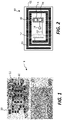
- a hybrid high-security document 10 includes a document 20 and a plurality of independent light-emitting modules 60 (i.e. wirelessly powered displays 60).
- the document 20 can be a conventional printed document such as a label, a commercial document such as a certificate, a stock certificate, a bond, or a bearer bond or a government-issued document such as a passport, a monetary instrument, or a license and can include additional anti-counterfeiting features such as are found in high-security documents.
- a high-security document is a document that includes a security feature and the document 20 can be a high-security document.
- a banknote 20 is a high-security document.
- High-security documents 20 include passports and identification cards such as driver's licenses or other government-issued identification.
- the term "banknote” is used synonymously with high-security document and any reference to “banknote” can also be a reference to a high-security document.
- the banknote 20 can be a government-issued banknote 20 and can include visible markings 22 such as value indicators, decorative elements, and anti-counterfeiting structures or markings.
- the light-emitting modules 60 are disposed on or embedded in the banknote 20, for example disposed on or embedded in the material on which the visible markings 22 are printed or disposed on or embedded in other elements of the banknote 20, such as a thread, ribbon, film, decal, or flexible substrate.
- Each light-emitting module 60 comprises an antenna 50 with multiple turns, an electronic circuit 40, and a light emitter 30 mounted and electrically connected on a substrate 62 separate and independent from the document except insofar as the one is affixed to the other. Referring also to Fig.
- each light-emitting module 60 includes an antenna 50, for example a near-field communication (NFC) antenna or an RFID antenna that provides electrical power to the electronic circuit 40 in response to received electromagnetic radiation so that the electronic circuit 40 is responsive to electrical power provided from the antenna 50 to control the light emitter 30 to emit light.
- NFC near-field communication
- the electronic circuit 40 and light emitter 30 are powered solely by the energy received from the antenna 50 and the electronic circuit 40 or hybrid high-security document 10 does not include any devices for storing energy between uses, such as a battery.
- the electronic circuit 40 can include a memory 44 for storing information.
- the electronic circuit 40 is connected to a light emitter 30 and includes circuitry for controlling the light emitter 30 to emit light when electrical power is provided from the antenna 50.
- the light-emitting module 60 can include a power converter that converts a signal with a relatively high current and low voltage to a signal with a relatively high voltage and low current.
- the light-emitting module 60 can also or alternatively include an acoustic wave filter 52 for converting the impedance of the electrical power provided from the antenna 50 in response to received electromagnetic radiation.
- the acoustic wave filter 52 can be the power converter.
- the electronic circuit 40, light emitter 30, and optional acoustic wave filter 52 can be mounted or otherwise disposed on a substrate 62, for example by micro-transfer printing.
- the antenna 50 can be formed on or in or disposed on the substrate 62.
- Electrical wires 64 can also be formed at least partly on or in the substrate 62 to electrically connect the antenna 50, optional acoustic wave filter 52, electronic circuit 40 and light emitter 30.
- the electronic circuit 40 can be, or is a part of, or can include an integrated circuit and, in an embodiment, can be or include a small micro-transfer printable integrated circuit such as a chiplet, or a semiconductor for example having an area less than 100,000, square microns.
- the light-emitting module 60 can be a small micro-transfer printable module, for example formed on a semiconductor or other substrate such as glass or plastic having an area less than 100,000, square microns.
- the acoustic wave filter 52 can be a surface acoustic wave filter (SAW) or bulk acoustic wave filter (BAW), for example including AIN, and the light emitter 30 can be an inorganic light-emitting diode (iLED) 32, for example made with a compound semiconductor such as GaN or AIGaN.
- SAW surface acoustic wave filter
- BAW bulk acoustic wave filter
- iLED inorganic light-emitting diode
- Micro-transfer printable iLED 32 devices can be formed in or on a source wafer 36 over a sacrificial portion of a sacrificial layer that, when etched, forms a tether 34 ( Fig. 3 ) connecting the micro-transfer printable device to an anchor portion of the wafer.
- a tether 34 Fig. 3
- the tether 34 is fractured so that a micro-transfer printed device has a fractured tether 34, as illustrated in Fig. 3.
- FIG 3 is a simple illustration of an iLED 32 with a fractured tether 34 over a sacrificial portion of a source wafer.
- the tether 34 is located beneath the micro-transfer printable device (e.g., inorganic light-emitting diode 32) or the micro-transfer printable device is held in place by the sacrificial portion to the anchor portion.
- the micro-transfer printable device e.g., inorganic light-emitting diode 32
- the substrate 62 of the light-emitting module 60 can be at least one of glass, plastic, polymer, resin, silicon, a semiconductor, and a compound semiconductor, or other suitable substrates. Any one or all of the optional acoustic wave filter 52, light emitter 30, and electronic circuit 40 can be assembled on the substrate 62 using micro-transfer printing and electrically interconnected with electrically conductive wires 64 using photolithographic methods and materials to form the light-emitting module 60.
- the light-emitting module 60 can, in turn be micro-transfer printed or otherwise printed, transferred, or assembled onto another substrate such as the banknote 20 to form the hybrid banknote 10 or on to an intermediate substrate such as a tape or reel for high-speed printing onto a sheet or web, such as a sheet or web of banknotes 20 or flexible substrates incorporated into banknotes 20.
- the banknote 20 includes a flexible substrate, ribbon, film, or thread (all of which are indicated as ribbon 70 herein) incorporated in, laminated to, woven into, or hot-press mounted onto the banknote 20.
- the independent light-emitting modules 60 are mounted on, embedded in, or micro-transfer printed onto the flexible substrate, ribbon 70, film, or thread.
- the flexible substrate, ribbon 70, film, or thread can include paper, plastic, impregnated paper, or metal foil and can be electrically insulating.
- the hybrid banknote 10 includes a plurality of light-emitting modules 60 and there is no electrical interconnection between the various light-emitting modules 60 so that each light-emitting module 60 is electrically separate, independent, and disconnected.
- Each light-emitting module 60 is electrically independent of all of the other light-emitting modules 60 and, other than, in one embodiment, having a common substrate 62 or being mounted on a common ribbon 70 or banknote 20, can also be spatially separated and physically independent and separated, although the light-emitting modules 60 can be arranged in a desired pattern.
- the light-emitting modules 60 can each have a separate substrate 62 ( Fig. 12 ) different from the banknote 20.
- the light-emitting modules 60 are, in accordance with the invention, disposed to form at least one of a character, a graphic indicator, an icon, a number, a letter, and a pictogram or indicates a value, a date, or a person.
- the graphic indicator can have semantic content, for example indicating a value, a date, or a person.
- the light-emitting modules 60 form a line.
- the banknote 20 can be a government-issued banknote 20 or other high-security document having visible markings 22 and the plurality of light-emitting modules 60 can be disposed in a location corresponding to a portion of the visible markings 22 to highlight or otherwise indicate the portion of the visible markings 22.
- the light emitter 30 can underline or surround a graphic element of the visible markings 22. As shown in Fig. 1 , the light-emitting modules 60 form the number 500, which matches the visible marking 22 printed on the banknote 20.
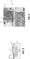
- the banknote is a banknote 20 having a denomination (e.g., five) and the light-emitting modules 60 are disposed to form the numeral 5 on the ribbon 70 laminated onto or woven into the banknote 20 making the hybrid banknote 10.
- the antenna 50 of each light-emitting module 60 will generate electrical power, optionally voltage amplified and filtered by the acoustic wave filter 52 ( Fig. 2 ), to the electronic circuit 40 to cause the light emitter 30 to emit light.
- the signal harvested from the antenna 50 is relatively small, it is helpful to have as long an antenna 50 extending with as many turns as possible in the light-emitting module 60 to provide enough power to light the light emitters 30. Because the light-emitting module 62 can be small and the antenna 50 needs to have a length matched to the frequency of the received signals, it can be necessary to have a large number of antenna turns. In an embodiment, the necessary number of turns are provided in a single layer; in another embodiment, multiple layers of antenna turns are provided. The signal received typically has a relatively smaller voltage and larger current.
- the acoustic wave filter 52 is also a power converter 52 that converts the received signal to a signal with a relatively larger voltage and smaller current more suitable for providing power to the electronic circuit 40 and for lighting the light emitter 30.
- the acoustic waver filter 52 is smaller than conventional acoustic waver filters, for example having an area less than 100, 50, 20, or 10 square microns suitable for micro-transfer printing and unsuitable for conventional transfer or printing methods and having a reduced number of acoustic resonant filter modes, for example a single dominant resonant mode.
- the NFC field will provide power to all of the light-emitting modules 60 at about the same time so that the light emitters 30 will emit light visibly simultaneously, in this case forming a visible numeral 5.
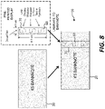
- a banknote 20 is provided in step 100, for example using conventional currency materials and printing technologies, and a light-emitting module source wafer (e.g., source wafer 36, Fig. 3 ) is provided in step 110, for example using photolithographic materials and techniques.
- the light-emitting modules 60 are provided in surface-mount accessible form, or on a tape or film.
- the light-emitting modules 60 are printed from the light-emitting module source wafer 36 or other source to the banknote 20 in step 120 to form the hybrid banknote 10.
- a banknote 20 is provided in step 100, for example using conventional currency materials and printing technologies, and a light-emitting module source is provided in step 110.
- a ribbon 70 is provided in step 130 and the light-emitting modules 60 are printed or otherwise disposed onto the ribbon 70 in step 140, for example by micro-transfer printing, by surface mount techniques, or from a tape and reel.
- the ribbon 70, with the light-emitting modules 60, is then integrated into the banknote 20 in step 150 to form the hybrid banknote 10 for example by lamination or hot-pressing.
- This process has the advantage of more-readily controlling the substrate (ribbon 70) on which the light-emitting modules 60 are micro-transfer printed and using conventional methods for integrating the ribbon 70 into the banknote 20.
- the plurality of light-emitting modules 60 include different inorganic light-emitting diodes 32 that emit different colors of light, for example red, green, and blue light.
- the different light-emitting modules 60 can be disposed in groups for a desired effect, for example each numeral or graphic element in the disposed arrangement of light-emitting modules 60 can have a different color.
- the electronic circuit 40 controls the light emitters in a light-emitting module 60 to flash once or to flash sequentially.
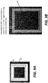
- Fig. 9A illustrates a receiving antenna 50 with multiple turns (windings, or coils) on the substrate 62 for a light-emitting module 60.
- Fig. 9B shows a typical NFC reader antenna 50 found in a smart cellular telephone or other NFC device.
- Fig. 9B illustrates the approximate size of the light-emitting module 60 relative to the size of the NFC reader antenna ( Fig. 9A ). As is apparent from the illustration, the physical size of the light-emitting module 60 is very small relative to the NFC reader antenna.
- Fig. 10 is a schematic illustrating in more detail the electronic circuit 40.
- the antenna 50 is electrically connected to the input of the acoustic wave filter 52 which filters and impedance converts the electrical signal from the antenna 50.
- the antenna 50 converts an externally generated NFC magnetic field into electrical power and the acoustic wave filter 52 is tuned to the desired electrical signal from the antenna 50 and multiplies the received electrical signal to a voltage sufficient to operate the electronic circuit 40.
- the output of the acoustic wave filter 52 is electrically connected to the electronic circuit 40, in this case including a rectifier and voltage multiplier that provides electrical current and a sufficient voltage through a current limiter to cause the inorganic light-emitting diode 32 to emit light.
- the electronic circuit 40 can rectify a 13.56 MHz radio frequency signal into DC voltage, increases the voltage further, for example with a voltage doubling circuit, and regulates the current to the iLED 32.
- the electronic circuit 40 can be a small integrated circuit such as a chiplet or, as shown, an application specific integrated circuit 66.
- the acoustic wave filter 52 is operated at a dimension of one-half wavelength and is used to implement an impedance transformer similar to that using ordinary electrical transmission lines.
- the acoustic wave filter 52 can operate at much smaller dimensions than electrical transmission lines utilizing only metallic conductors and typical dielectric mediums.
- the acoustic velocity of the acoustic wave filter 52 is only on the order of 3000 to 6000 meters per second and can therefore implement a half-wave transmission line in a distance of 0.5 mm or less for a given NFC frequency such as 13.56 MHz with a quality factor (Q) on the order of 1000 or more.
- the half-wave element may be acoustically grounded at two ends and driven near one end by the very low impedance antenna 50.
- a high impedance output is available at the center of the acoustic wave filter 52.
- the output voltage of antenna 50 is on the order of a few millivolts which is insufficient to power the electronic circuit 40.
- the acoustic wave filter 52 converts the low antenna 50 voltage via the half-wave transmission line and its associated high Q to a much higher output voltage of 0.5 volt or greater which is sufficient to energize the electronic circuit 40.
- Figs. 11A and 11B are perspectives illustrating the antenna 50, electronic circuit 40, acoustic wave filter 52 and light emitter 30 disposed on the substrate 62 to make up the light-emitting module 60.
- the light-emitting module 60 structure of Figs. 11A and 11B can have a length and a width less than 0.5 mm and a height less than 25 microns. Because the light-emitting module 60 structure is relatively small and does not require any external electrical connections, it is very robust under mechanical stress, for example when folded, spindled, or crumpled.
- the banknote 20 tends to be more flexible than the light-emitting module 60 (although the elements and substrate 62 of the light-emitting module 60 can be somewhat flexible) and will preferentially flex, reducing the stress on the light-emitting modules 60.
- Fig. 12 illustrates an embodiment of the present invention in cross section.
- the light-emitting module 60 is disposed on a ribbon 70 that is laminated to the banknote 20 (not shown) with the light-emitting module 60 between the ribbon 70 and the banknote 20.
- the iLED 32 emits light through the ribbon 70 so the ribbon 70 must be at least partially transparent to the frequency of emitted light, for example 50%, 60%, 70%, 80%, 90%, or 95% transparent.
- This construction protects the light-emitting module 60 from environmental or mechanical damage.
- Such a module can be assembled using compound micro-assembly techniques. For example, a glass wafer is provided with a patterned sacrificial layer and a substrate layer to form the substrate 62.
- the iLED 32, an integrated circuit incorporating the electronic circuit 40, and the acoustic wave filter 52 are each micro-transfer printed from individual different source wafers to the glass wafer (substrate 62).
- electrically conductive wires 64 are patterned over the components and the glass wafer, for example by evaporating or sputtering an aluminum metallization layer and pattern-wise etching (using optically sensitive photoresist and optical masks) the metal layer to form the antenna 50 and wires 64.
- a dielectric is deposited, for example silicon dioxide using sputtering or evaporation, or by coating or laminating a layer of a dielectric material such as SU8.
- the process can be repeated multiple times to make a multi-layer antenna 50 with an increased number of turns.
- Electrical connections can be formed by etching vias and patterning deposited metal in the vias.
- a passivation layer can be provided for environmental protection.
- the substrate 62 and the components can have a thickness of only a few microns and the completed structure can have a thickness of less than 35 ⁇ m.
- the light-emitting modules 60 can be formed over a patterned sacrificial layer for micro-transfer printing. The patterned sacrificial layer is etched to form the tethers 34 and the micro-transfer printable light-emitting modules 60 (as in Fig. 3 ). A stamp is pressed against the light-emitting modules 60, fractures the tether 34, and transfers the light-emitting modules 60 to a destination substrate such as the ribbon 70 (step 140 of Fig. 7 ).
- the light emitter 30 e.g., an iLED
- the acoustic wave filter 52 can be formed in different materials for example AIN for the acoustic wave filter 52, a compound semiconductor such as GaAs or InGaN for the light emitter 30 (e.g., an iLED), and silicon for the ASIC 66.
- a source wafer e.g., iLED source wafer 36 for each of these devices in a suitable material is formed in steps 300, 310, and 320, respectively.
- An intermediate substrate e.g., substrate 62
- the light emitters 30, the acoustic wave filter 52, and the ASIC 66 are each micro-transfer printed onto the substrate 62 in steps 330, 340, and 350, respectively, but can be transferred in any desired order. If any or all of the devices are micro-transfer printed, each will include a fractured tether 34 ( Fig. 3 ). Alternatively, other transfer methods can be used. After the devices are all transferred to the substrate 62, electrical connections can be formed, for example using photolithographic methods to form electrical connections such as wires 64, in step 360, as well as the antenna 50.
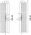
- the antenna 50 is a multi-layer antenna. Since the signal captured by the antenna 50 is partly dependent on the number of turns, or coils or windings, in the antenna 50, it can be useful to increase the number of such turns to increase the signal magnitude.
- multiple layers 51 of antenna turns are separated by dielectric layers with each antenna layer 51 connected to an adjoining antenna layer 51, for example through a via (not shown).
- adjoining antenna layers 51 are connected alternately near the edge and near the center of the antenna 50, thus reducing the number of layers and vias needed.
- the number of layers 51 in the multi-layer antenna 50 is even, as shown in Figs.
- each end of the loop antenna 50 can be electrically connected to the electronic circuit 40, forming a loop antenna 50 or providing a relative ground for the electronic circuit 40.
- the electrical connections to the electronic circuit 40 from the antenna 50 can be at or near the center of the substrate 62, as shown.
- the antenna layers 51 are alternately connected near the edge of the antenna 50 and near the center of the antenna 50, where the center of the antenna 50 is near the center of the spiral formed by the turns of the electrical conductor forming the antenna 50.
- the antenna layer 51 farthest from the electronic circuit 40 is electrically connected to the electronic circuit layer nearer the center of the antenna layer 51 than the edge of the antenna layer 51.
- the dielectric layers keep the various layers 51 of antenna turns from electrically shorting together or electrically shorting to the light emitters 30, the acoustic wave filter 52, the ASIC 66, or the wires 64 (collectively devices, the wires 64 are not shown in Figs. 20, 21 ).
- the dielectric layers can be formed by coating, embossing, and filling, e.g., with curable conductive ink, photolithographic deposition and patterning, or laminating subsequent layers of materials, for example a curable resin or other plastic layer and can encapsulate the electrical conductor making up the antenna 50.
- a laminated layer can include an antenna layer 51.
- the vias between and connecting layers 51 can be formed with photolithography or can be a part of the layer applied.
- the devices are formed or disposed on the substrate 62 and the layers 51 of antenna turns are formed in the same layer and above the devices so that the electronic circuit 40 is located between the antenna portion and the banknote 20 and at least a portion of the antenna 50 is located on a side of the electronic circuit 40 opposite the banknote 20.
- the devices are directly beneath (or above) one or more of the antenna turns, reducing the area of the light-emitting modules 60.
- the substrate 62 is then disposed on or adhered to the ribbon 70 in step 370, for example by micro-transfer printing, or by other means, so that the light emitters 30 emit light through the ribbon 70.
- the same process can be used to make the multi-layer antenna 50 and device structure, but the top antenna 50 layer is disposed or adhered to the ribbon 70, so that the light emitters 30 emit light in a direction opposite the ribbon 70.
- a portion of the antenna 50 is located between the integrated circuit 66 and the banknote 20 (ribbon 70).
- the ribbon 70 is incorporated into a banknote 20.
- a plurality of substrates 62 can each be provided and the light-emitting module 60 made individually on each substrate 62.
- the substrate 62 is originally much larger than the light-emitting module 60 and multiple light-emitting modules 60 are formed on a common substrate 62 at the same time using the same process steps, such as micro-transfer printing, photolithographic steps, and coating.
- the substrate 62 can then be diced, for example by scribing and breaking, diamond saw cutting, or laser cutting, to form the individual light-emitting modules 60, such as surface-mount devices.
- the light-emitting modules 60 are micro-transfer printable light-emitting modules 60 formed over sacrificial portions of a sacrificial layer and fastened with tethers 34 to anchors on the substrate 62.
- the individual light-emitting modules 60 are then disposed on the ribbons 70 using micro-transfer printing stamps to contact the light-emitting modules 60, the tethers 34 are fractured, the light-emitting modules 60 are transferred to the ribbon 70, the light-emitting modules 60 are applied to the ribbon 70 to adhere them to the ribbon 70 (for example on an adhesive layer on the ribbon 70), and the stamp is removed.
- the devices can be disposed on the substrates 62 using micro-transfer printing.
- the substrates 62 are diced to provide individual light-emitting modules 60
- the devices can be disposed on the substrates 62 using micro-transfer printing.
- the light-emitting modules 60 are also micro-transfer printed (rather than just the devices from the source substrate 36)
- a web of ribbons 70 can be one meter in width and the substrate 62 can be a similar size, thereby reducing the number of micro-transfer printing steps necessary to dispose a light-emitting module 60 on each ribbon 70.
- one or more light emitters 30, an integrated circuit 66 or, optionally, an acoustic wave filter 52 are micro-transfer printed onto a substrate 62 to form a light-emitting module 60 and the light-emitting modules 60 incorporate the substrate 62.
- a plurality of the one or more light emitters 30, integrated circuits 66 or optional acoustic wave filters 52 are micro-transfer printed onto the substrate 62 to form light-emitting modules 60.
- the light-emitting modules 60 are, in turn, micro-transfer printed onto the banknote 20 or onto a flexible substrate, film, thread, or ribbon 70 subsequently incorporated in, laminated to, or woven into the banknote 20.
- a plurality of the light-emitting modules 60 can be micro-transfer printed from the substrate 62 onto a plurality of the banknotes 20 or onto one or more of flexible substrates (e.g., ribbon 70) in a single step, for example in a web and a roll-to-roll process.
- the substrate 62 has an area or dimension that is equal to or larger than a corresponding area or dimension of the documents 20, e.g., banknotes 20 or flexible substrates, e.g. ribbons 70.
- the substrate 62 can have a width or length dimension that is at least as large as the width of the web.
- the substrate 62 can have an extent (for example an x or y dimension, length or width, but not a thickness or z dimension) or area that is within a range of one tenth to ten times an extent or area of the flexible substrate (for example a width of a web), within a range of one quarter to four times an extent or area of the flexible substrate, within a range of one half to two times an extent or area of the flexible substrate, or within 25%, 10%, or 5% of an extent or area of the flexible substrate.
- an extent for example an x or y dimension, length or width, but not a thickness or z dimension
- area that is within a range of one tenth to ten times an extent or area of the flexible substrate (for example a width of a web), within a range of one quarter to four times an extent or area of the flexible substrate, within a range of one half to two times an extent or area of the flexible substrate, or within 25%, 10%, or 5% of an extent or area of the flexible substrate.
- a hybrid banknote 10 according to the structure of Fig. 12 can be constructed by first providing a roll of polyimide film (1302).
- the light-emitting modules 60 are micro-transfer printed onto separated portions of the polyimide layer (1304), which acts as the ribbon 70.
- the different components of the light-emitting module 60 are micro-transfer printed onto the roll of polyimide film itself and processed photolithographically to complete the light-emitting modules 60 so that the polyimide film serves as the substrate 62 (not shown) and can be a common substrate for multiple light-emitting modules 60.
- the roll of polyimide file is sprayed with a protective layer (1306) and a thermoset adhesive layer (1308) and slit into strips (1310). Each strip is then cut into portions suitable for each banknote 20, applied to the banknote 20, and heated to complete the hybrid banknote 10 (1312).
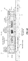
- Fig. 14 is a table presenting various design choices to enable a corresponding variety of functional embodiments of the present invention.
- Table 14 provides example antenna 50 dimensions based on the power required by an iLED 32 load.
- small antennas 50 suitable for small light-emitting modules 60 generate small output voltages that can be increased using acoustic wave filters 52 operating in a resonance condition.
- An increased voltage of 0.5 V is sufficient to be converted with a charge pump in the electronic circuit 40 to drive an iLED 32 at 0.3 ⁇ A at 3.3 V.
- the light-emitting module 60 structure of the present invention disposed on the banknote 20 can be generally employed in multi-element light-emitting systems.
- a multi-element light-emitting system comprises a plurality of independent light-emitting modules 60, each independent light-emitting module 60 including an antenna 50 with multiple turns, an electronic circuit 40, and a light emitter 30 mounted and electrically connected on a separate substrate 62.
- the independent light-emitting modules 60 are disposed in a pattern to form a visible indicator and can be disposed on a variety of underlying structures including, but not limited to, banknotes 20.
- the light-emitting modules 60 of the present invention emit light when the light-emitting modules 60 are located in an NFC magnetic field.
- a hybrid banknote mat 80 comprising a mat circuit 84 and an antenna 50 (not shown but similar to those found in existing NFC terminals or smart phones, e.g., Fig. 9B ).
- the form factor of the mat 80 is not limited to any specific form factor and can be similar in structure to any NFC reader / writer.
- the mat circuit 84 provides a continuous or pulsed NFC signal, the pulsed NFC signal having a pulse rate of ten, twenty, fifty, or one hundred pulses per second or greater.
- the NFC field can operate for 2 msec out of every 20 msec and a 50 Hz frequency.
- Each such NFC circuit can drive thousands of light-emitting modules 60 to emit light, enabling a wide variety of patterns, applications, and effects.
- the mat 80 can include a display 82 responsive to the mat circuit 84.
- the hybrid banknote 10 of the present invention can also be interacted with by conventional NFC devices.
- the electronic circuit 40 stores information in the memory 44, for example serial number information, value information, manufacturing information, usage information, or location information.
- This information can be retrieved using RFID or NFC techniques and read, for example by the mat 80 and the information, or an aggregation of the information, displayed on the mat 80 with the the display 82.
- the mat display 82 can display the sum of the values of the hybrid banknotes 10 located on or very near the mat 80.
- the mat 80 can also include switches, buttons, or other user-interactive devices for controlling the mat 80 to perform various desired functions or select options.
- options can include displaying value, serial number, or manufacturing date, location of the hybrid banknote 10.
- Information can be encrypted, can be changed (if the memory 44 includes writable or rewritable memory).
- a device for example the mat 80, can write information into the electronic circuit.
- the information can also be communicated to and stored in an information registry independent of the hybrid high-security document 10 or banknote 20. If the information is a value, the banknote 20 can then have the stored value rather than a denomination printed on the banknote 20.
- the mat 80 can be a part of a cash register or management system and can detect the value and serial identification of the hybrid banknotes 10 in the system to provide a currency inventory.
- a cash register system can provide security and theft detection.
- Hybrid banknotes 10 that have missing or non-functional light-emitting modules 60 can be detected by comparing the number of detected light-emitting modules 60 to the expected number of light-emitting modules 60.
- a hybrid banknote 10 can even be deactivated or the light-emitting modules 60 can be placed in a deactivated state.
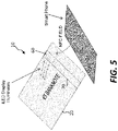
- a method of using a hybrid banknote 10 comprises the steps of providing a hybrid banknote 10 in step 200, exposing the hybrid banknote 10 to an electromagnetic field so that the antenna 50 provides power to the electronic circuit 40 and causes the light emitter 30 to emit light in step 210, and observing or detecting the light in step 220.
- the electromagnetic field is provided by the mat 80 in step 215, the electronic circuit 40 stores information, for example in the memory 44, the information is read from the hybrid banknote 10 in step 217, and the display 82 is responsive to the information.
- the information from the hybrid banknote 10 is transferred to a computer system for action or processing in step 230. Information can also be written into a hybrid banknote 10.
- the electronic circuit 40 can also be an integrated circuit, for example a small chiplet, suitable for micro-transfer printing.
- the electronic circuit 40 can include digital circuits or logic (for example CMOS circuits) and power circuits (for example for driving an LED).
- the electronic circuit 40 can include information storage circuits, a state machine, or a stored program machine to implement the desired functionality of the hybrid banknote 10.
- the electronic circuit 40 can read or write information such as currency values, process information, respond to input and provide output.
- the iLEDs 32 and electronic circuit 40 are too small to be readily visible with the unaided human eye.
- the iLEDs 32 and electronic circuit 40 can be located in areas of the banknote 20 that include visible markings 22 to further obscure the presence of the iLEDs 32 and electronic circuit 40, as well as any wires 64.
- any of the iLEDs 32, electronic circuit 40, or wires 64 are marked with visible markings 22.
- ink can be printed over the non-emitting side of the iLEDs 32, electronic circuit 40, or wires 64 to obscure them or otherwise make them a part of the visible markings 22 on the banknote 20.
- the iLEDs 32, electronic circuit 40, or wires 64 can each be very small, for example having a size in the micron range, they can be effectively invisible to the unaided human eye.
- the one or more inorganic micro light-emitting diodes 32 or the electronic circuit 40 of the hybrid banknote 10 can have a width from 2 to 5 ⁇ m, 5 to 10 ⁇ m, 10 to 20 ⁇ m, or 20 to 50 ⁇ m, a length from 2 to 5 ⁇ m, 5 to 10 ⁇ m, 10 to 20 ⁇ m, or 20 to 50 ⁇ m, or a height from 2 to 5 ⁇ m, 4 to 10 ⁇ m, 10 to 20 ⁇ m, or 20 to 50 ⁇ m.
- the hybrid banknote 10 includes visible markings 22 that do not include a value.
- a hybrid banknote 10 can be a non-denominational banknote 20 that either has an assigned value or a variable value stored in a memory 44 in the electronic circuit 40.
- the memory 44 can be a read-only memory that encodes a desired assigned value.
- the assigned value can be a currency value or can include an electronic serial number, or both.
- the memory 44 can be a write-once memory 44 that stores multiple values in memory locations that are ordered in a sequential order, for example by memory address.
- the write-once memory 44 can, for example, employ fuses that are electrically destroyed and cannot be rewritten.
- the memory 44 can be a non-volatile read-write memory.
- the value stored by the hybrid banknote 10 can change over time.
- the current value can be modified by, for example, a teller machine. If a change in the current value of the hybrid banknote 10 is desired, an input value can be input by a user with an input device.
- a teller machine controller can then calculate or otherwise determine a new stored value responsive to the input value and store the new value in the hybrid banknote 10, for example by communicating the new stored value to the electronic circuit 40 which then writes the new stored value in the memory 44.
- the electronic circuit 40 only writes new stored values in the memory 44 that are smaller than the current value.
- the electronic circuit 40 can write new stored values in the memory 44 that are larger than the current value, or that are larger than the current value but are limited to a maximum value.
- the change in current value of the hybrid banknote 10 can represent or be the result of a financial transaction, for example a purchase or a financial exchange with or facilitated by a financial institution such as a bank or government institution such as a central bank.
- Read-only memories, write-once memories, and read/write memories together with controllers and read/write circuitry can be formed in integrated circuits and electrical circuits.
- Devices for currency handling, optical inspection, displays, input devices (such as keyboards or touch screens) can be made using electromechanical, electronic, and optical technologies.
- An assigned or current value can be programmed into the electronic circuit 40 or an associated memory 44 (also micro-transfer printed if it is a separate integrated circuit or chiplet) either before or after the electronic circuit 40 or memory 44 is micro-transfer printed.
- an external device such as a hybrid banknote teller machine (that can be a part of or include, for example, a mat 80) can communicate with the electronic circuit 40 to write an assigned or current value to the hybrid banknote 10.
- a hybrid banknote 10 teller machine can also communicate with a central or remote database to establish the legitimacy of the hybrid banknote 10, track its use or location, or approve a transaction and record or approve the transaction.
- the communication can include an electronic serial number.
- the light-emitting modules 60 of the hybrid high-security document 10 are wirelessly powered displays 60.
- the wirelessly powered display 60 comprises a substrate 62.
- One or more light-emitters 30 e.g., inorganic light-emitting diodes 32
- An antenna with multiple turns and an electronic circuit are also disposed on the substrate.
- the electronic circuit is electrically connected to the one or more inorganic LEDs and the antenna, the antenna is responsive to electromagnetic energy to provide electrical power to the wirelessly powered display 60
- the electronic circuit 40 includes a power converter 52 that converts a signal with a relatively high current and low voltage to a signal with a relatively high voltage and low current.
- the wirelessly powered display 60 excludes a battery, internal power source, or wired power source and the wirelessly powered display 60 operates solely on the electrical power provided through the antenna 50.
- a plurality of light-emitting modules form a single wirelessly powered display 60.
- each light-emitting module 60 forms a single wirelessly powered display 60.
- a plurality of light-emitting modules are provided on a common substrate 62 and comprise one or a plurality of wirelessly powered displays 60.
- each of the light-emitting modules 60 in Fig. 1 is a separate wirelessly powered display 60.
- the light-emitting modules 60 of Fig. 1 form a single wirelessly powered display 60.
- the light-emitting modules 60 can each have a separate substrate 62 or are provided on a common substrate 62.
- the converted signal can provide power to the light-emitters 30 of the pixels and to a display controller 46 that controls the light-emitters 30.
- the display controller 46 can be a portion of the electronic circuit 40 ( Fig. 2 ).
- the wirelessly powered display 60 displays a fixed image, that is, when wireless power is provided to wirelessly powered display 60, the wirelessly powered display 60 will display a still image that cannot be changed or reprogrammed. When wireless power is not provided, no image is displayed.
- the display controller 46 can display a variable image, for example a blinking image, a series of stored independent still images, or a series of images representing a moving image or image sequence.
- the display controller 46 can receive wireless signals comprising an image or sequence of images and display the image or images.
- the wirelessly powered display 60 can have a single pixel with one light emitter 30 or multiple light emitters 30 emitting the same or different colors of light.
- the wirelessly powered display 60 has multiple pixels with one light emitter 30 or multiple light emitters 30 emitting the same or different colors of light.
- the wirelessly powered display 60 is a sticker, includes a sticker, or has a substrate 62 that is a sticker.
- a sticker is an adhesive substrate 62 on which the wirelessly powered display 60 is provided, disposed, or formed.
- the substrate 62 can be rigid or flexible, and the adhesive can be permanent, temporary, or removable so that the wirelessly powered display 60 is permanently adhered to a surface, temporarily adhered to a surface, or removably adhered to a surface.
- wirelessly powered display 60 comprises an acoustic wave filter, a surface acoustic wave filter, or a bulk acoustic wave filter.
- a wirelessly coupled display system 86 comprises a device (e.g., a mat 80 or a smart phone) including a wireless power transmitter (e.g., a portion of the mat circuit 84) that provides wireless power within a specified range (e.g., the wireless power transmitter is a near-field communication NFC device and provides a continuous or pulsed NFC signal).
- a wireless power transmitter e.g., a portion of the mat circuit 84
- the wireless power transmitter is a near-field communication NFC device and provides a continuous or pulsed NFC signal.
- One or more wirelessly powered displays 60 are located within the range and are responsive to the wireless power provided by the device to display an image.
- the device is a portable device, the device is a mobile device, the display is in a fixed location, or the display is mobile or affixed to a mobile or portable device.
- the wirelessly powered display 60 is mounted on the device.
- the device can include a primary device display and the wirelessly powered display 60 is a secondary display mounted on or incorporated into the device.
- the one or more wirelessly powered displays 60 are physically separate from the device.
- the device can be a mobile telephone or a smart phone and can be moved from a remote location outside the range to a location within the range to provide wireless power to the wirelessly powered display 60 and cause the wirelessly powered display 60 to display an image.
- the device can include a stored image and an image transmitter circuit (e.g., a portion of the mat circuit 84) that wirelessly provides the stored image to the wirelessly powered display 60 and the wirelessly powered display 60 is responsive to the wirelessly provided image to display the image.
- the electronic circuit 40 of the wirelessly powered display 60 can include a display controller 46 ( Fig. 2 ).
- a wirelessly coupled display system 86 includes one wirelessly powered display 60 or a plurality of wirelessly powered displays 60.
- Each wirelessly powered display 60 can have an identification and a circuit (e.g., a portion of the electronic circuit 40) for responding to the identification when the identification is transmitted.
- the device can include a transmitter circuit (e.g., a portion of the mat circuit 84) that wirelessly provides one or more of the identifications to the one or more wirelessly powered displays 60.
- Embodiments of the present invention enable a variety of low-cost wirelessly powered displays 60 that are inactive until a device, such as a smart phone, come into range and provide wireless power to activate the wirelessly powered display 60 to provide information, for example information local or contextual to the wirelessly powered display 60. Since the wirelessly powered displays 60 do not have an independent external power source they can be located in a wide variety of places not associated with powered devices (e.g., remote from an electrical power transmission grid) and since the wirelessly powered displays 60 do not have an internal power source (e.g., a battery) they can have a very long lifetime.
- a device such as a smart phone
- U.S. Patent Application Serial No. 14/743,981 filed June 18, 2015 , entitled Micro Assembled Micro LED Displays and Lighting Elements , describes micro-transfer printing structures and processes useful with the present invention.
- micro-transfer printing techniques see also U.S. Patent Nos. 8,722,458 , 7,622,367 and 8,506,867 .
- Micro-transfer printing using compound micro assembly structures and methods can also be used with the present invention, for example, as described in U.S. Patent Application Serial No. 14/822,868, filed August 10, 2015 , entitled Compound Micro-Assembly Strategies and Devices .
- a first layer on a second layer in some embodiments means a first layer directly on and in contact with a second layer. In other embodiments, a first layer on a second layer can include another layer there between.
Landscapes
- Engineering & Computer Science (AREA)
- Physics & Mathematics (AREA)
- General Physics & Mathematics (AREA)
- Health & Medical Sciences (AREA)
- General Health & Medical Sciences (AREA)
- Toxicology (AREA)
- Computer Hardware Design (AREA)
- Theoretical Computer Science (AREA)
- Computer Networks & Wireless Communication (AREA)
- Microelectronics & Electronic Packaging (AREA)
- Spectroscopy & Molecular Physics (AREA)
- Signal Processing (AREA)
- Electromagnetism (AREA)
- Computer Vision & Pattern Recognition (AREA)
- Computer Security & Cryptography (AREA)
- Acoustics & Sound (AREA)
- Power Engineering (AREA)
- Credit Cards Or The Like (AREA)
- Inspection Of Paper Currency And Valuable Securities (AREA)
- Control Of Indicators Other Than Cathode Ray Tubes (AREA)
- Transceivers (AREA)
Description
- The present invention relates to a hybrid high-security document with electronically controlled inorganic-light-emitting diode displays operated using wirelessly transmitted power.
- Monetary instruments issued by governments such as money or currency are used throughout the world today. Government-issued currency typically includes banknotes (also known as paper currency or bills) having visible markings printed on high-quality paper, plastic, or paper impregnated with other materials, such as plastic. The visible markings indicate the denomination (value) of the banknote and include a serial number, decorations such as images, and anti-counterfeiting structures such as special threads, ribbons, and holograms. Currency circulates within an economic system as a medium of monetary exchange having a fixed value until it is physically worn out. Worn out banknotes are generally returned by banks or other financial institutions and then replaced.
- Other privately issued monetary instruments, such as credit cards and gift cards, are also used by the public. These cards typically include an electronically accessible value (e.g., stored in a magnetic stripe or in a chip in the card) or an electronically accessible account that can be used to make purchases. However, the electronically stored value of the card is not readily viewed by a user.
- In the past, banknotes have not been electronically enabled. However, more recently there have been proposals to use RFID (radio-frequency identification device) in banknotes to validate the banknote and avoid counterfeiting. For example,
U.S. Patent No. 8,391,688 andU.S. Patent No. 8,791,822 disclose systems for currency validation.U.S. Patent No. 5,394,969 describes a capacitance-based verification device for a security thread embedded within currency paper to defeat counterfeiting. Security systems for scanning a paper banknote and checking identification information in the banknote (e.g., the serial number) with a network-accessible database have been proposed, for example inU.S. Patent No. 6,131,718 . Further examples of hybrid high-security documents incorporating electronic circuits are disclosed inUS2005/0150740 A1 andDE 10 2013 102003 A1 . - Near-field-communications (NFC) systems also provide an electronic response to electromagnetic stimulation for enabling financial transactions by employing a set of electromagnetic communication protocols that enable two electronic devices, one of which is usually a portable device such as a smartphone, to communicate by bringing them within 4 cm of each other. These devices use electromagnetic induction between two loop antennae to communicate and transmit power, for example as disclosed in
U.S. Patent 7,688,270 . Thus, at least one of the devices can operate without a stored energy device such as a battery. In all of these systems, however, there is no way to visibly and electronically test attributes of a banknote. - There remains a need, therefore, for currency with visible indicia that is electronically accessible.
- The present invention provides a hybrid high-security document, including: a document; a plurality of independent light-emitting modules disposed on or embedded in the document, each module including: an antenna with multiple turns, an electronic circuit, and a light emitter mounted and electrically connected on a substrate separate from the document, wherein the electronic circuit is responsive to electrical power provided from the antenna to control the light emitter to emit light. The light emitting modules of the plurality of light emitting modules are electrically independent and electrically disconnected from each other.
- In certain embodiments, the electronic circuit is formed in a micro-transfer printed integrated circuit having a fractured tether, wherein the light emitter is formed in a micro-transfer printed semiconductor having a fractured tether, or wherein the light-emitting module is a micro-transfer printed module having a fractured tether.
- In certain embodiments, the electronic circuit is formed in a micro-transfer printed integrated circuit or semiconductor that has an area less than one hundred thousand square microns.
- In certain embodiments, the light-emitting module has an area less than one hundred thousand square microns.
- In certain embodiments, the hybrid high-security document includes a power converter that converts a signal with a relatively high current and low voltage to a signal with a relatively high voltage and low current.
- In certain embodiments, the power converter is a micro-transfer printed power converter having a fractured tether.
- In certain embodiments, the hybrid high-security document includes an acoustic wave filter, a surface acoustic wave filter, or a bulk acoustic wave filter.
- In certain embodiments, the acoustic wave filter has a single dominant acoustic resonant filter mode.
- In certain embodiments, the acoustic wave filter is a micro-transfer printed acoustic wave filter having a fractured tether.
- In accordance with the invention, the light-emitting modules of the plurality of light-emitting modules are disposed to form at least one of a character, a graphic indicator, an icon, a number, a letter, and a pictogram or indicates a value, a date, or a person.
- In certain embodiments, the document has visible markings and the one or more light-emitting modules are disposed in a location corresponding to a portion of the visible markings to highlight or otherwise indicate or emphasize the portion of the visible markings.
- In certain embodiments, the electronic circuit is responsive to power received by the antenna to cause the light emitter to emit light or to send an electromagnetic signal.
- In certain embodiments, the antenna is a multi-layer antenna formed in multiple layers.
- In certain embodiments, the multi-layer antenna includes an even number of layers.
- In certain embodiments, the antenna layers are alternately connected near the edge of the antenna and near the center of the antenna.
- In certain embodiments, the electronic circuit is in a layer and the antenna layer farthest from the electronic circuit is electrically connected to the electronic circuit layer nearer to the center of the electronic circuit layer than to the edge of the electronic circuit layer.
- The foregoing and other objects, aspects, features, and advantages of the present disclosure will become more apparent and better understood by referring to the following description taken in conjunction with the accompanying drawings, in which:
-
Fig. 1 is a plan view of the front and back sides of a hybrid banknote in an embodiment of the present invention; -
Fig. 2 is a schematic diagram according to an embodiment of the present invention; -
Fig. 3 is a schematic illustration of a light emitter with a fractured tether according to an embodiment of the present invention; -
Fig. 4 is a plan view of the front and back sides of another embodiment of the present invention; -
Fig. 5 is a schematic illustration of operating an embodiment of the present invention; -
Figs. 6-7 are flow charts illustrating methods of the present invention; -
Fig. 8 is a schematic diagram illustrating a method of making an embodiment of the present invention; -
Figs. 9A and 9B are schematic illustrations of antennae according to embodiments of the present invention; -
Fig. 10 is a schematic diagram illustrating a circuit according to an embodiment of the present invention; -
Fig. 11A is a perspective according to an embodiment of the present invention andFig. 11B is a corresponding, less-detailed and more accurate perspective at a larger scale; -
Fig. 12 is a cross section of an embodiment of the present invention; -
Fig. 13 is a flow graph illustrating a method of the present invention; -
Fig. 14 is a table showing design alternatives according to corresponding embodiments of the present invention; -
Fig. 15 is a perspective according to an embodiment of the present invention; -
Fig. 16 is a timing diagram according to an embodiment of the present invention; -
Figs. 17 and 18 are flow charts illustrating methods of the present invention; -
Fig. 19 is a flow chart illustrating a method of the present invention; and -
Figs. 20 and 21 are cross sections illustrating arrangements of the antenna and integrated circuits of the present invention. - The features and advantages of the present disclosure will become more apparent from the detailed description set forth below when taken in conjunction with the drawings, in which like reference characters identify corresponding elements throughout. In the drawings, like reference numbers generally indicate identical, functionally similar, and/or structurally similar elements. The figures are not drawn to scale since the variation in size of various elements in the Figures is too great to permit depiction to scale.
- Referring to
Fig. 1 , in an embodiment of the present invention a hybrid high-security document 10 includes adocument 20 and a plurality of independent light-emitting modules 60 (i.e. wirelessly powered displays 60). Thedocument 20 can be a conventional printed document such as a label, a commercial document such as a certificate, a stock certificate, a bond, or a bearer bond or a government-issued document such as a passport, a monetary instrument, or a license and can include additional anti-counterfeiting features such as are found in high-security documents. A high-security document is a document that includes a security feature and thedocument 20 can be a high-security document. In an embodiment, and as described herein, abanknote 20 is a high-security document. Other high-security documents 20 include passports and identification cards such as driver's licenses or other government-issued identification. As used herein, the term "banknote" is used synonymously with high-security document and any reference to "banknote" can also be a reference to a high-security document. Thebanknote 20 can be a government-issuedbanknote 20 and can includevisible markings 22 such as value indicators, decorative elements, and anti-counterfeiting structures or markings. - The light-emitting
modules 60 are disposed on or embedded in thebanknote 20, for example disposed on or embedded in the material on which thevisible markings 22 are printed or disposed on or embedded in other elements of thebanknote 20, such as a thread, ribbon, film, decal, or flexible substrate. Each light-emittingmodule 60 comprises anantenna 50 with multiple turns, anelectronic circuit 40, and alight emitter 30 mounted and electrically connected on asubstrate 62 separate and independent from the document except insofar as the one is affixed to the other. Referring also toFig. 2 , each light-emittingmodule 60 includes anantenna 50, for example a near-field communication (NFC) antenna or an RFID antenna that provides electrical power to theelectronic circuit 40 in response to received electromagnetic radiation so that theelectronic circuit 40 is responsive to electrical power provided from theantenna 50 to control thelight emitter 30 to emit light. In an embodiment, theelectronic circuit 40 andlight emitter 30 are powered solely by the energy received from theantenna 50 and theelectronic circuit 40 or hybrid high-security document 10 does not include any devices for storing energy between uses, such as a battery. - The
electronic circuit 40 can include amemory 44 for storing information. Theelectronic circuit 40 is connected to alight emitter 30 and includes circuitry for controlling thelight emitter 30 to emit light when electrical power is provided from theantenna 50. The light-emittingmodule 60 can include a power converter that converts a signal with a relatively high current and low voltage to a signal with a relatively high voltage and low current. The light-emittingmodule 60 can also or alternatively include anacoustic wave filter 52 for converting the impedance of the electrical power provided from theantenna 50 in response to received electromagnetic radiation. Theacoustic wave filter 52 can be the power converter. Theelectronic circuit 40,light emitter 30, and optionalacoustic wave filter 52 can be mounted or otherwise disposed on asubstrate 62, for example by micro-transfer printing. Theantenna 50 can be formed on or in or disposed on thesubstrate 62.Electrical wires 64 can also be formed at least partly on or in thesubstrate 62 to electrically connect theantenna 50, optionalacoustic wave filter 52,electronic circuit 40 andlight emitter 30. - The electronic circuit 40 (and optional memory 44) can be, or is a part of, or can include an integrated circuit and, in an embodiment, can be or include a small micro-transfer printable integrated circuit such as a chiplet, or a semiconductor for example having an area less than 100,000, square microns. In a further embodiment, the light-emitting
module 60 can be a small micro-transfer printable module, for example formed on a semiconductor or other substrate such as glass or plastic having an area less than 100,000, square microns. Theacoustic wave filter 52 can be a surface acoustic wave filter (SAW) or bulk acoustic wave filter (BAW), for example including AIN, and thelight emitter 30 can be an inorganic light-emitting diode (iLED) 32, for example made with a compound semiconductor such as GaN or AIGaN. - Micro-transfer
printable iLED 32 devices (or other devices e.g., chiplets, integrated circuits, or acoustic wave filters 52) can be formed in or on asource wafer 36 over a sacrificial portion of a sacrificial layer that, when etched, forms a tether 34 (Fig. 3 ) connecting the micro-transfer printable device to an anchor portion of the wafer. When transferred by a printing stamp from the wafer to a destination substrate, such as thesubstrate 62, thetether 34 is fractured so that a micro-transfer printed device has a fracturedtether 34, as illustrated inFig. 3. Fig. 3 is a simple illustration of aniLED 32 with a fracturedtether 34 over a sacrificial portion of a source wafer. In other embodiments, thetether 34 is located beneath the micro-transfer printable device (e.g., inorganic light-emitting diode 32) or the micro-transfer printable device is held in place by the sacrificial portion to the anchor portion. - The
substrate 62 of the light-emittingmodule 60 can be at least one of glass, plastic, polymer, resin, silicon, a semiconductor, and a compound semiconductor, or other suitable substrates. Any one or all of the optionalacoustic wave filter 52,light emitter 30, andelectronic circuit 40 can be assembled on thesubstrate 62 using micro-transfer printing and electrically interconnected with electricallyconductive wires 64 using photolithographic methods and materials to form the light-emittingmodule 60. The light-emittingmodule 60, with its various components including thesubstrate 62, can, in turn be micro-transfer printed or otherwise printed, transferred, or assembled onto another substrate such as thebanknote 20 to form thehybrid banknote 10 or on to an intermediate substrate such as a tape or reel for high-speed printing onto a sheet or web, such as a sheet or web ofbanknotes 20 or flexible substrates incorporated intobanknotes 20. Referring toFig. 4 , in an embodiment of the invention, thebanknote 20 includes a flexible substrate, ribbon, film, or thread (all of which are indicated asribbon 70 herein) incorporated in, laminated to, woven into, or hot-press mounted onto thebanknote 20. The independent light-emittingmodules 60 are mounted on, embedded in, or micro-transfer printed onto the flexible substrate,ribbon 70, film, or thread. The flexible substrate,ribbon 70, film, or thread can include paper, plastic, impregnated paper, or metal foil and can be electrically insulating. - In accordance with the invention, the
hybrid banknote 10 includes a plurality of light-emittingmodules 60 and there is no electrical interconnection between the various light-emittingmodules 60 so that each light-emittingmodule 60 is electrically separate, independent, and disconnected. Each light-emittingmodule 60 is electrically independent of all of the other light-emittingmodules 60 and, other than, in one embodiment, having acommon substrate 62 or being mounted on acommon ribbon 70 orbanknote 20, can also be spatially separated and physically independent and separated, although the light-emittingmodules 60 can be arranged in a desired pattern. The light-emittingmodules 60 can each have a separate substrate 62 (Fig. 12 ) different from thebanknote 20. The light-emittingmodules 60 are, in accordance with the invention, disposed to form at least one of a character, a graphic indicator, an icon, a number, a letter, and a pictogram or indicates a value, a date, or a person. The graphic indicator can have semantic content, for example indicating a value, a date, or a person. For example, inFig. 4 , the light-emittingmodules 60 form a line. Thebanknote 20 can be a government-issuedbanknote 20 or other high-security document havingvisible markings 22 and the plurality of light-emittingmodules 60 can be disposed in a location corresponding to a portion of thevisible markings 22 to highlight or otherwise indicate the portion of thevisible markings 22. For example, thelight emitter 30 can underline or surround a graphic element of thevisible markings 22. As shown inFig. 1 , the light-emittingmodules 60 form thenumber 500, which matches thevisible marking 22 printed on thebanknote 20. - Referring to
Fig. 5 , in an example embodiment, the banknote is abanknote 20 having a denomination (e.g., five) and the light-emittingmodules 60 are disposed to form thenumeral 5 on theribbon 70 laminated onto or woven into thebanknote 20 making thehybrid banknote 10. When thehybrid banknote 10 is placed near a near-field-communication field, for example a near-field-communication field generated by a smartphone or other NFC device, theantenna 50 of each light-emittingmodule 60 will generate electrical power, optionally voltage amplified and filtered by the acoustic wave filter 52 (Fig. 2 ), to theelectronic circuit 40 to cause thelight emitter 30 to emit light. Because the signal harvested from theantenna 50 is relatively small, it is helpful to have as long anantenna 50 extending with as many turns as possible in the light-emittingmodule 60 to provide enough power to light thelight emitters 30. Because the light-emittingmodule 62 can be small and theantenna 50 needs to have a length matched to the frequency of the received signals, it can be necessary to have a large number of antenna turns. In an embodiment, the necessary number of turns are provided in a single layer; in another embodiment, multiple layers of antenna turns are provided. The signal received typically has a relatively smaller voltage and larger current. Thus, in an embodiment, theacoustic wave filter 52 is also apower converter 52 that converts the received signal to a signal with a relatively larger voltage and smaller current more suitable for providing power to theelectronic circuit 40 and for lighting thelight emitter 30. In a further embodiment of the present invention, theacoustic waver filter 52 is smaller than conventional acoustic waver filters, for example having an area less than 100, 50, 20, or 10 square microns suitable for micro-transfer printing and unsuitable for conventional transfer or printing methods and having a reduced number of acoustic resonant filter modes, for example a single dominant resonant mode. Although the light-emittingmodules 60 are electrically separate and independent, the NFC field will provide power to all of the light-emittingmodules 60 at about the same time so that thelight emitters 30 will emit light visibly simultaneously, in this case forming avisible numeral 5. - Referring to
Fig. 6 , in an embodiment of the present invention, abanknote 20 is provided instep 100, for example using conventional currency materials and printing technologies, and a light-emitting module source wafer (e.g.,source wafer 36,Fig. 3 ) is provided instep 110, for example using photolithographic materials and techniques. Alternatively, the light-emittingmodules 60 are provided in surface-mount accessible form, or on a tape or film. The light-emittingmodules 60 are printed from the light-emittingmodule source wafer 36 or other source to thebanknote 20 instep 120 to form thehybrid banknote 10. Alternatively, referring to bothFig. 7 andFig. 8 , abanknote 20 is provided instep 100, for example using conventional currency materials and printing technologies, and a light-emitting module source is provided instep 110. Aribbon 70 is provided instep 130 and the light-emittingmodules 60 are printed or otherwise disposed onto theribbon 70 instep 140, for example by micro-transfer printing, by surface mount techniques, or from a tape and reel. Theribbon 70, with the light-emittingmodules 60, is then integrated into thebanknote 20 in step 150 to form thehybrid banknote 10 for example by lamination or hot-pressing. This process has the advantage of more-readily controlling the substrate (ribbon 70) on which the light-emittingmodules 60 are micro-transfer printed and using conventional methods for integrating theribbon 70 into thebanknote 20. - In an embodiment, the plurality of light-emitting
modules 60 include different inorganic light-emittingdiodes 32 that emit different colors of light, for example red, green, and blue light. The different light-emittingmodules 60 can be disposed in groups for a desired effect, for example each numeral or graphic element in the disposed arrangement of light-emittingmodules 60 can have a different color. In an embodiment, theelectronic circuit 40 controls the light emitters in a light-emittingmodule 60 to flash once or to flash sequentially. -
Fig. 9A illustrates a receivingantenna 50 with multiple turns (windings, or coils) on thesubstrate 62 for a light-emittingmodule 60.Fig. 9B shows a typicalNFC reader antenna 50 found in a smart cellular telephone or other NFC device.Fig. 9B illustrates the approximate size of the light-emittingmodule 60 relative to the size of the NFC reader antenna (Fig. 9A ). As is apparent from the illustration, the physical size of the light-emittingmodule 60 is very small relative to the NFC reader antenna. -
Fig. 10 is a schematic illustrating in more detail theelectronic circuit 40. Theantenna 50 is electrically connected to the input of theacoustic wave filter 52 which filters and impedance converts the electrical signal from theantenna 50. Theantenna 50 converts an externally generated NFC magnetic field into electrical power and theacoustic wave filter 52 is tuned to the desired electrical signal from theantenna 50 and multiplies the received electrical signal to a voltage sufficient to operate theelectronic circuit 40. The output of theacoustic wave filter 52 is electrically connected to theelectronic circuit 40, in this case including a rectifier and voltage multiplier that provides electrical current and a sufficient voltage through a current limiter to cause the inorganic light-emittingdiode 32 to emit light. For example, theelectronic circuit 40 can rectify a 13.56 MHz radio frequency signal into DC voltage, increases the voltage further, for example with a voltage doubling circuit, and regulates the current to theiLED 32. Theelectronic circuit 40 can be a small integrated circuit such as a chiplet or, as shown, an application specificintegrated circuit 66. - The
acoustic wave filter 52 is operated at a dimension of one-half wavelength and is used to implement an impedance transformer similar to that using ordinary electrical transmission lines. Theacoustic wave filter 52 can operate at much smaller dimensions than electrical transmission lines utilizing only metallic conductors and typical dielectric mediums. The acoustic velocity of theacoustic wave filter 52 is only on the order of 3000 to 6000 meters per second and can therefore implement a half-wave transmission line in a distance of 0.5 mm or less for a given NFC frequency such as 13.56 MHz with a quality factor (Q) on the order of 1000 or more. The half-wave element may be acoustically grounded at two ends and driven near one end by the verylow impedance antenna 50. A high impedance output is available at the center of theacoustic wave filter 52. The output voltage ofantenna 50 is on the order of a few millivolts which is insufficient to power theelectronic circuit 40. Theacoustic wave filter 52 converts thelow antenna 50 voltage via the half-wave transmission line and its associated high Q to a much higher output voltage of 0.5 volt or greater which is sufficient to energize theelectronic circuit 40. -
Figs. 11A and 11B are perspectives illustrating theantenna 50,electronic circuit 40,acoustic wave filter 52 andlight emitter 30 disposed on thesubstrate 62 to make up the light-emittingmodule 60. For example, the light-emittingmodule 60 structure ofFigs. 11A and 11B can have a length and a width less than 0.5 mm and a height less than 25 microns. Because the light-emittingmodule 60 structure is relatively small and does not require any external electrical connections, it is very robust under mechanical stress, for example when folded, spindled, or crumpled. Thebanknote 20 tends to be more flexible than the light-emitting module 60 (although the elements andsubstrate 62 of the light-emittingmodule 60 can be somewhat flexible) and will preferentially flex, reducing the stress on the light-emittingmodules 60. -
Fig. 12 illustrates an embodiment of the present invention in cross section. As shown inFig. 12 , the light-emittingmodule 60 is disposed on aribbon 70 that is laminated to the banknote 20 (not shown) with the light-emittingmodule 60 between theribbon 70 and thebanknote 20. TheiLED 32 emits light through theribbon 70 so theribbon 70 must be at least partially transparent to the frequency of emitted light, for example 50%, 60%, 70%, 80%, 90%, or 95% transparent. This construction protects the light-emittingmodule 60 from environmental or mechanical damage. Such a module can be assembled using compound micro-assembly techniques. For example, a glass wafer is provided with a patterned sacrificial layer and a substrate layer to form thesubstrate 62. TheiLED 32, an integrated circuit incorporating theelectronic circuit 40, and theacoustic wave filter 52 are each micro-transfer printed from individual different source wafers to the glass wafer (substrate 62). Using photolithographic techniques, electricallyconductive wires 64 are patterned over the components and the glass wafer, for example by evaporating or sputtering an aluminum metallization layer and pattern-wise etching (using optically sensitive photoresist and optical masks) the metal layer to form theantenna 50 andwires 64. A dielectric is deposited, for example silicon dioxide using sputtering or evaporation, or by coating or laminating a layer of a dielectric material such as SU8. The process can be repeated multiple times to make amulti-layer antenna 50 with an increased number of turns. Electrical connections (wires 64) can be formed by etching vias and patterning deposited metal in the vias. A passivation layer can be provided for environmental protection. Thesubstrate 62 and the components can have a thickness of only a few microns and the completed structure can have a thickness of less than 35 µm. The light-emittingmodules 60 can be formed over a patterned sacrificial layer for micro-transfer printing. The patterned sacrificial layer is etched to form thetethers 34 and the micro-transfer printable light-emitting modules 60 (as inFig. 3 ). A stamp is pressed against the light-emittingmodules 60, fractures thetether 34, and transfers the light-emittingmodules 60 to a destination substrate such as the ribbon 70 (step 140 ofFig. 7 ). - Referring to
Fig. 19 in more detail, the light emitter 30 (e.g., an iLED), theacoustic wave filter 52, and theASIC 66 can be formed in different materials for example AIN for theacoustic wave filter 52, a compound semiconductor such as GaAs or InGaN for the light emitter 30 (e.g., an iLED), and silicon for theASIC 66. A source wafer (e.g., iLED source wafer 36) for each of these devices in a suitable material is formed insteps light emitters 30, theacoustic wave filter 52, and theASIC 66 are each micro-transfer printed onto thesubstrate 62 insteps Fig. 3 ). Alternatively, other transfer methods can be used. After the devices are all transferred to thesubstrate 62, electrical connections can be formed, for example using photolithographic methods to form electrical connections such aswires 64, instep 360, as well as theantenna 50. - Referring to
Figs. 20 and 21 , in further embodiments of the present invention, theantenna 50 is a multi-layer antenna. Since the signal captured by theantenna 50 is partly dependent on the number of turns, or coils or windings, in theantenna 50, it can be useful to increase the number of such turns to increase the signal magnitude. In the simplified illustration ofFig. 20 , multiple layers 51 of antenna turns are separated by dielectric layers with each antenna layer 51 connected to an adjoining antenna layer 51, for example through a via (not shown). In an embodiment, adjoining antenna layers 51 are connected alternately near the edge and near the center of theantenna 50, thus reducing the number of layers and vias needed. In an embodiment, the number of layers 51 in themulti-layer antenna 50 is even, as shown inFigs. 20 and 21 so that each end of theloop antenna 50 can be electrically connected to theelectronic circuit 40, forming aloop antenna 50 or providing a relative ground for theelectronic circuit 40. The electrical connections to theelectronic circuit 40 from theantenna 50 can be at or near the center of thesubstrate 62, as shown. Thus, in an embodiment, the antenna layers 51 are alternately connected near the edge of theantenna 50 and near the center of theantenna 50, where the center of theantenna 50 is near the center of the spiral formed by the turns of the electrical conductor forming theantenna 50. Moreover, in an embodiment the antenna layer 51 farthest from theelectronic circuit 40 is electrically connected to the electronic circuit layer nearer the center of the antenna layer 51 than the edge of the antenna layer 51. The dielectric layers keep the various layers 51 of antenna turns from electrically shorting together or electrically shorting to thelight emitters 30, theacoustic wave filter 52, theASIC 66, or the wires 64 (collectively devices, thewires 64 are not shown inFigs. 20, 21 ). The dielectric layers can be formed by coating, embossing, and filling, e.g., with curable conductive ink, photolithographic deposition and patterning, or laminating subsequent layers of materials, for example a curable resin or other plastic layer and can encapsulate the electrical conductor making up theantenna 50. A laminated layer can include an antenna layer 51. The vias between and connecting layers 51 can be formed with photolithography or can be a part of the layer applied. - In the embodiment of
Fig. 20 , the devices are formed or disposed on thesubstrate 62 and the layers 51 of antenna turns are formed in the same layer and above the devices so that theelectronic circuit 40 is located between the antenna portion and thebanknote 20 and at least a portion of theantenna 50 is located on a side of theelectronic circuit 40 opposite thebanknote 20. In a particular embodiment, the devices are directly beneath (or above) one or more of the antenna turns, reducing the area of the light-emittingmodules 60. Thesubstrate 62 is then disposed on or adhered to theribbon 70 instep 370, for example by micro-transfer printing, or by other means, so that thelight emitters 30 emit light through theribbon 70. In the embodiment ofFig. 21 , the same process can be used to make themulti-layer antenna 50 and device structure, but thetop antenna 50 layer is disposed or adhered to theribbon 70, so that thelight emitters 30 emit light in a direction opposite theribbon 70. In this case, a portion of theantenna 50 is located between theintegrated circuit 66 and the banknote 20 (ribbon 70). Instep 380, theribbon 70 is incorporated into abanknote 20. - A plurality of
substrates 62 can each be provided and the light-emittingmodule 60 made individually on eachsubstrate 62. In a more efficient process, thesubstrate 62 is originally much larger than the light-emittingmodule 60 and multiple light-emittingmodules 60 are formed on acommon substrate 62 at the same time using the same process steps, such as micro-transfer printing, photolithographic steps, and coating. Thesubstrate 62 can then be diced, for example by scribing and breaking, diamond saw cutting, or laser cutting, to form the individual light-emittingmodules 60, such as surface-mount devices. However, it is an advantage of the present invention that very small light-emittingmodules 60 can be formed so that conventional methods of separating individual light-emittingmodules 60 or disposing light-emittingmodules 60 onto aribbon 70 can be difficult. Therefore, in an embodiment of the present invention, the light-emittingmodules 60 are micro-transfer printable light-emittingmodules 60 formed over sacrificial portions of a sacrificial layer and fastened withtethers 34 to anchors on thesubstrate 62. The individual light-emittingmodules 60 are then disposed on theribbons 70 using micro-transfer printing stamps to contact the light-emittingmodules 60, thetethers 34 are fractured, the light-emittingmodules 60 are transferred to theribbon 70, the light-emittingmodules 60 are applied to theribbon 70 to adhere them to the ribbon 70 (for example on an adhesive layer on the ribbon 70), and the stamp is removed. - In the case in which the
substrates 62 are diced to provide individual light-emittingmodules 60, the devices can be disposed on thesubstrates 62 using micro-transfer printing. In this case, to reduce the number of print steps, it is useful to provide asubstrate 62 whose size is on the order of thesource wafer 36 size so that many devices from eachsource wafer 36 can be transferred in a single stamp transfer step. However, in an embodiment in which the light-emittingmodules 60 are also micro-transfer printed (rather than just the devices from the source substrate 36), it is useful to provide asubstrate 62 whose size is on the order of a web ofribbons 70 that are destination substrates for the micro-transfer process. For example, if theribbons 70 are 2 mm in width and it is desired to micro-transfer print five hundred light-emittingmodules 60 at a time, a web ofribbons 70 can be one meter in width and thesubstrate 62 can be a similar size, thereby reducing the number of micro-transfer printing steps necessary to dispose a light-emittingmodule 60 on eachribbon 70. - In other embodiments of the present invention, one or more
light emitters 30, anintegrated circuit 66 or, optionally, anacoustic wave filter 52 are micro-transfer printed onto asubstrate 62 to form a light-emittingmodule 60 and the light-emittingmodules 60 incorporate thesubstrate 62. In a further embodiment, a plurality of the one or morelight emitters 30,integrated circuits 66 or optional acoustic wave filters 52 are micro-transfer printed onto thesubstrate 62 to form light-emittingmodules 60. The light-emittingmodules 60 are, in turn, micro-transfer printed onto thebanknote 20 or onto a flexible substrate, film, thread, orribbon 70 subsequently incorporated in, laminated to, or woven into thebanknote 20. A plurality of the light-emittingmodules 60 can be micro-transfer printed from thesubstrate 62 onto a plurality of thebanknotes 20 or onto one or more of flexible substrates (e.g., ribbon 70) in a single step, for example in a web and a roll-to-roll process. In an embodiment, thesubstrate 62 has an area or dimension that is equal to or larger than a corresponding area or dimension of thedocuments 20, e.g.,banknotes 20 or flexible substrates,e.g. ribbons 70. For example, if theribbons 70 orbanknotes 20 are provided in a web, thesubstrate 62 can have a width or length dimension that is at least as large as the width of the web. Thesubstrate 62 can have an extent (for example an x or y dimension, length or width, but not a thickness or z dimension) or area that is within a range of one tenth to ten times an extent or area of the flexible substrate (for example a width of a web), within a range of one quarter to four times an extent or area of the flexible substrate, within a range of one half to two times an extent or area of the flexible substrate, or within 25%, 10%, or 5% of an extent or area of the flexible substrate. By providing asubstrate 62 having a size that is the same order of magnitude, comparable, or larger than the destination substrate of the micro-transfer printing step, the number of separate print steps can be reduced since each print step can transfer more light-emittingmodules 60. - Referring to
Fig. 13 , in an embodiment of the present invention, ahybrid banknote 10 according to the structure ofFig. 12 can be constructed by first providing a roll of polyimide film (1302). The light-emittingmodules 60 are micro-transfer printed onto separated portions of the polyimide layer (1304), which acts as theribbon 70. Alternatively, the different components of the light-emittingmodule 60 are micro-transfer printed onto the roll of polyimide film itself and processed photolithographically to complete the light-emittingmodules 60 so that the polyimide film serves as the substrate 62 (not shown) and can be a common substrate for multiple light-emittingmodules 60. The roll of polyimide file is sprayed with a protective layer (1306) and a thermoset adhesive layer (1308) and slit into strips (1310). Each strip is then cut into portions suitable for eachbanknote 20, applied to thebanknote 20, and heated to complete the hybrid banknote 10 (1312). - In the present invention, it is important that the
antenna 50 provide sufficient power to theelectronic circuit 40 to cause thelight emitter 30 to emit light.Fig. 14 is a table presenting various design choices to enable a corresponding variety of functional embodiments of the present invention. Table 14 providesexample antenna 50 dimensions based on the power required by aniLED 32 load. As shown,small antennas 50 suitable for small light-emittingmodules 60 generate small output voltages that can be increased using acoustic wave filters 52 operating in a resonance condition. An increased voltage of 0.5 V is sufficient to be converted with a charge pump in theelectronic circuit 40 to drive aniLED 32 at 0.3 µA at 3.3 V. - The light-emitting
module 60 structure of the present invention disposed on thebanknote 20 can be generally employed in multi-element light-emitting systems. For example, in an embodiment of the present invention, a multi-element light-emitting system comprises a plurality of independent light-emittingmodules 60, each independent light-emittingmodule 60 including anantenna 50 with multiple turns, anelectronic circuit 40, and alight emitter 30 mounted and electrically connected on aseparate substrate 62. The independent light-emittingmodules 60 are disposed in a pattern to form a visible indicator and can be disposed on a variety of underlying structures including, but not limited to,banknotes 20. - The light-emitting
modules 60 of the present invention emit light when the light-emittingmodules 60 are located in an NFC magnetic field. Referring toFig. 15 , such a field can be provided by ahybrid banknote mat 80, comprising amat circuit 84 and an antenna 50 (not shown but similar to those found in existing NFC terminals or smart phones, e.g.,Fig. 9B ). Although illustrated as a largely planar mat, the form factor of themat 80 is not limited to any specific form factor and can be similar in structure to any NFC reader / writer. Themat circuit 84 provides a continuous or pulsed NFC signal, the pulsed NFC signal having a pulse rate of ten, twenty, fifty, or one hundred pulses per second or greater. This pulse rate is much higher than those found in conventional NFC terminals or smart phones so that the light-emittingmodules 60 of the present invention will emit light at a sufficient frequency as to be visible to the human eye. As illustrated inFig. 16 , the NFC field can operate for 2 msec out of every 20 msec and a 50 Hz frequency. Each such NFC circuit can drive thousands of light-emittingmodules 60 to emit light, enabling a wide variety of patterns, applications, and effects. Themat 80 can include adisplay 82 responsive to themat circuit 84. Thehybrid banknote 10 of the present invention can also be interacted with by conventional NFC devices. - In a further embodiment of the present invention, the
electronic circuit 40 stores information in thememory 44, for example serial number information, value information, manufacturing information, usage information, or location information. This information can be retrieved using RFID or NFC techniques and read, for example by themat 80 and the information, or an aggregation of the information, displayed on themat 80 with the thedisplay 82. For example, themat display 82 can display the sum of the values of thehybrid banknotes 10 located on or very near themat 80. Themat 80 can also include switches, buttons, or other user-interactive devices for controlling themat 80 to perform various desired functions or select options. For example, options can include displaying value, serial number, or manufacturing date, location of thehybrid banknote 10. Information can be encrypted, can be changed (if thememory 44 includes writable or rewritable memory). Thus, in an embodiment, a device, for example themat 80, can write information into the electronic circuit. The information can also be communicated to and stored in an information registry independent of the hybrid high-security document 10 orbanknote 20. If the information is a value, thebanknote 20 can then have the stored value rather than a denomination printed on thebanknote 20. - The
mat 80 can be a part of a cash register or management system and can detect the value and serial identification of thehybrid banknotes 10 in the system to provide a currency inventory. Such a cash register system can provide security and theft detection.Hybrid banknotes 10 that have missing or non-functional light-emittingmodules 60 can be detected by comparing the number of detected light-emittingmodules 60 to the expected number of light-emittingmodules 60. Ahybrid banknote 10 can even be deactivated or the light-emittingmodules 60 can be placed in a deactivated state. - In a further embodiment of the present invention and as illustrated in
Fig. 17 , a method of using ahybrid banknote 10 comprises the steps of providing ahybrid banknote 10 instep 200, exposing thehybrid banknote 10 to an electromagnetic field so that theantenna 50 provides power to theelectronic circuit 40 and causes thelight emitter 30 to emit light instep 210, and observing or detecting the light in step 220. In an alternative embodiment and as shown inFig. 18 , the electromagnetic field is provided by themat 80 instep 215, theelectronic circuit 40 stores information, for example in thememory 44, the information is read from thehybrid banknote 10 instep 217, and thedisplay 82 is responsive to the information. Alternatively, the information from thehybrid banknote 10 is transferred to a computer system for action or processing instep 230. Information can also be written into ahybrid banknote 10. - The
electronic circuit 40 can also be an integrated circuit, for example a small chiplet, suitable for micro-transfer printing. Theelectronic circuit 40 can include digital circuits or logic (for example CMOS circuits) and power circuits (for example for driving an LED). Theelectronic circuit 40 can include information storage circuits, a state machine, or a stored program machine to implement the desired functionality of thehybrid banknote 10. Theelectronic circuit 40 can read or write information such as currency values, process information, respond to input and provide output. - In a further embodiment, the
iLEDs 32 andelectronic circuit 40 are too small to be readily visible with the unaided human eye. Furthermore, theiLEDs 32 andelectronic circuit 40 can be located in areas of thebanknote 20 that includevisible markings 22 to further obscure the presence of theiLEDs 32 andelectronic circuit 40, as well as anywires 64. In one embodiment, any of theiLEDs 32,electronic circuit 40, orwires 64 are marked withvisible markings 22. For example, ink can be printed over the non-emitting side of theiLEDs 32,electronic circuit 40, orwires 64 to obscure them or otherwise make them a part of thevisible markings 22 on thebanknote 20. Since theiLEDs 32,electronic circuit 40, orwires 64 can each be very small, for example having a size in the micron range, they can be effectively invisible to the unaided human eye. For example, the one or more inorganic micro light-emittingdiodes 32 or theelectronic circuit 40 of thehybrid banknote 10 can have a width from 2 to 5 µm, 5 to 10 µm, 10 to 20 µm, or 20 to 50 µm, a length from 2 to 5 µm, 5 to 10 µm, 10 to 20 µm, or 20 to 50 µm, or a height from 2 to 5 µm, 4 to 10 µm, 10 to 20 µm, or 20 to 50 µm. - In another embodiment of the present invention, the
hybrid banknote 10 includesvisible markings 22 that do not include a value. Such ahybrid banknote 10 can be anon-denominational banknote 20 that either has an assigned value or a variable value stored in amemory 44 in theelectronic circuit 40. Thememory 44 can be a read-only memory that encodes a desired assigned value. The assigned value can be a currency value or can include an electronic serial number, or both. - In the case in which the assigned value is variable, the
memory 44 can be a write-once memory 44 that stores multiple values in memory locations that are ordered in a sequential order, for example by memory address. The write-once memory 44 can, for example, employ fuses that are electrically destroyed and cannot be rewritten. Alternatively, thememory 44 can be a non-volatile read-write memory. In this case, the value stored by thehybrid banknote 10 can change over time. The current value can be modified by, for example, a teller machine. If a change in the current value of thehybrid banknote 10 is desired, an input value can be input by a user with an input device. A teller machine controller can then calculate or otherwise determine a new stored value responsive to the input value and store the new value in thehybrid banknote 10, for example by communicating the new stored value to theelectronic circuit 40 which then writes the new stored value in thememory 44. In an embodiment, theelectronic circuit 40 only writes new stored values in thememory 44 that are smaller than the current value. In another embodiment, theelectronic circuit 40 can write new stored values in thememory 44 that are larger than the current value, or that are larger than the current value but are limited to a maximum value. The change in current value of thehybrid banknote 10 can represent or be the result of a financial transaction, for example a purchase or a financial exchange with or facilitated by a financial institution such as a bank or government institution such as a central bank. Read-only memories, write-once memories, and read/write memories together with controllers and read/write circuitry can be formed in integrated circuits and electrical circuits. Devices for currency handling, optical inspection, displays, input devices (such as keyboards or touch screens) can be made using electromechanical, electronic, and optical technologies. - An assigned or current value can be programmed into the
electronic circuit 40 or an associated memory 44 (also micro-transfer printed if it is a separate integrated circuit or chiplet) either before or after theelectronic circuit 40 ormemory 44 is micro-transfer printed. Alternatively, an external device such as a hybrid banknote teller machine (that can be a part of or include, for example, a mat 80) can communicate with theelectronic circuit 40 to write an assigned or current value to thehybrid banknote 10. Ahybrid banknote 10 teller machine can also communicate with a central or remote database to establish the legitimacy of thehybrid banknote 10, track its use or location, or approve a transaction and record or approve the transaction. The communication can include an electronic serial number. - In further embodiments of the present invention, the light-emitting
modules 60 of the hybrid high-security document 10 are wirelessly powered displays 60. The wirelesslypowered display 60 comprises asubstrate 62. One or more light-emitters 30 (e.g., inorganic light-emitting diodes 32) can form one or more pixels in the wirelesslypowered display 60. An antenna with multiple turns and an electronic circuit are also disposed on the substrate. The electronic circuit is electrically connected to the one or more inorganic LEDs and the antenna, the antenna is responsive to electromagnetic energy to provide electrical power to the wirelesslypowered display 60, and theelectronic circuit 40 includes apower converter 52 that converts a signal with a relatively high current and low voltage to a signal with a relatively high voltage and low current. In an embodiment of the present invention, the wirelesslypowered display 60 excludes a battery, internal power source, or wired power source and the wirelesslypowered display 60 operates solely on the electrical power provided through theantenna 50. - In one configuration of the present invention, a plurality of light-emitting modules form a single wirelessly
powered display 60. In another embodiment, each light-emittingmodule 60 forms a single wirelesslypowered display 60. In yet another embodiment, a plurality of light-emitting modules are provided on acommon substrate 62 and comprise one or a plurality of wirelessly powered displays 60. Thus, in one embodiment, each of the light-emittingmodules 60 inFig. 1 is a separate wirelesslypowered display 60. In an alternative configuration, the light-emittingmodules 60 ofFig. 1 form a single wirelesslypowered display 60. The light-emittingmodules 60 can each have aseparate substrate 62 or are provided on acommon substrate 62. - The converted signal can provide power to the light-
emitters 30 of the pixels and to adisplay controller 46 that controls the light-emitters 30. Thedisplay controller 46 can be a portion of the electronic circuit 40 (Fig. 2 ). In an embodiment, the wirelesslypowered display 60 displays a fixed image, that is, when wireless power is provided to wirelesslypowered display 60, the wirelesslypowered display 60 will display a still image that cannot be changed or reprogrammed. When wireless power is not provided, no image is displayed. Alternatively, thedisplay controller 46 can display a variable image, for example a blinking image, a series of stored independent still images, or a series of images representing a moving image or image sequence. Alternatively, thedisplay controller 46 can receive wireless signals comprising an image or sequence of images and display the image or images. - In various embodiments, the wirelessly
powered display 60 can have a single pixel with onelight emitter 30 or multiplelight emitters 30 emitting the same or different colors of light. Alternatively, the wirelesslypowered display 60 has multiple pixels with onelight emitter 30 or multiplelight emitters 30 emitting the same or different colors of light. - In one configuration, the wirelessly
powered display 60 is a sticker, includes a sticker, or has asubstrate 62 that is a sticker. As intended herein, a sticker is anadhesive substrate 62 on which the wirelesslypowered display 60 is provided, disposed, or formed. Thesubstrate 62 can be rigid or flexible, and the adhesive can be permanent, temporary, or removable so that the wirelesslypowered display 60 is permanently adhered to a surface, temporarily adhered to a surface, or removably adhered to a surface. - In an embodiment, wirelessly
powered display 60 comprises an acoustic wave filter, a surface acoustic wave filter, or a bulk acoustic wave filter. - In an embodiment of the present invention, a wirelessly coupled
display system 86 comprises a device (e.g., amat 80 or a smart phone) including a wireless power transmitter (e.g., a portion of the mat circuit 84) that provides wireless power within a specified range (e.g., the wireless power transmitter is a near-field communication NFC device and provides a continuous or pulsed NFC signal). One or more wirelesslypowered displays 60 are located within the range and are responsive to the wireless power provided by the device to display an image. In various embodiments, the device is a portable device, the device is a mobile device, the display is in a fixed location, or the display is mobile or affixed to a mobile or portable device. - In one embodiment, the wirelessly
powered display 60 is mounted on the device. For example, the device can include a primary device display and the wirelesslypowered display 60 is a secondary display mounted on or incorporated into the device. In another embodiment, the one or more wirelesslypowered displays 60 are physically separate from the device. The device can be a mobile telephone or a smart phone and can be moved from a remote location outside the range to a location within the range to provide wireless power to the wirelesslypowered display 60 and cause the wirelesslypowered display 60 to display an image. - The device can include a stored image and an image transmitter circuit (e.g., a portion of the mat circuit 84) that wirelessly provides the stored image to the wirelessly
powered display 60 and the wirelesslypowered display 60 is responsive to the wirelessly provided image to display the image. To facilitate the process, theelectronic circuit 40 of the wirelesslypowered display 60 can include a display controller 46 (Fig. 2 ). - In an embodiment of the present invention, a wirelessly coupled
display system 86 includes one wirelesslypowered display 60 or a plurality of wirelessly powered displays 60. Each wirelesslypowered display 60 can have an identification and a circuit (e.g., a portion of the electronic circuit 40) for responding to the identification when the identification is transmitted. The device can include a transmitter circuit (e.g., a portion of the mat circuit 84) that wirelessly provides one or more of the identifications to the one or more wirelessly powered displays 60. - Embodiments of the present invention enable a variety of low-cost wirelessly
powered displays 60 that are inactive until a device, such as a smart phone, come into range and provide wireless power to activate the wirelesslypowered display 60 to provide information, for example information local or contextual to the wirelesslypowered display 60. Since the wirelesslypowered displays 60 do not have an independent external power source they can be located in a wide variety of places not associated with powered devices (e.g., remote from an electrical power transmission grid) and since the wirelesslypowered displays 60 do not have an internal power source (e.g., a battery) they can have a very long lifetime. -
U.S. Patent Application Serial No. 14/743,981, filed June 18, 2015 U.S. Patent Nos. 8,722,458 ,7,622,367 and8,506,867 . Micro-transfer printing using compound micro assembly structures and methods can also be used with the present invention, for example, as described inU.S. Patent Application Serial No. 14/822,868, filed August 10, 2015 - As is understood by those skilled in the art, the terms "over", "under", "above", "below", "beneath", and "on" are relative terms and can be interchanged in reference to different orientations of the layers, elements, and substrates included in the present invention. For example, a first layer on a second layer, in some embodiments means a first layer directly on and in contact with a second layer. In other embodiments, a first layer on a second layer can include another layer there between.
- Having described certain embodiments, it will now become apparent to one of skill in the art that other embodiments incorporating the concepts of the disclosure may be used. Therefore, the invention is not limited to the described embodiments, but only by the scope of the following claims.
- The various described embodiments of the invention may be used in conjunction with one or more other embodiments unless technically incompatible.
- Throughout the description, where apparatus and systems are described as having, including, or comprising specific components, or where processes and methods are described as having, including, or comprising specific steps, it is contemplated that, additionally, there are apparatus, and systems of the disclosed technology that consist essentially of, or consist of, the recited components, and that there are processes and methods according to the disclosed technology that consist essentially of, or consist of, the recited processing steps.
- It should be understood that the order of steps or order for performing certain action is immaterial so long as the disclosed technology remains operable. Moreover, two or more steps or actions in some circumstances can be conducted simultaneously. The invention has been described in detail with particular reference to certain embodiments thereof, but it will be understood that variations and modifications can be effected within the scope of the invention as defined by the following claims.
-
- 10
- hybrid banknote / hybrid high-security document
- 20
- banknote / document / high-security document
- 22
- visible markings
- 30
- light emitter
- 32
- inorganic light-emitting diode
- 34
- tether
- 36
- iLED source wafer
- 40
- electronic circuit
- 44
- memory
- 46
- display controller
- 50
- antenna
- 51
- antenna layer
- 52
- power converter / acoustic wave filter
- 60
- light-emitting module / wirelessly powered display
- 62
- substrate
- 64
- wires
- 66
- ASIC
- 70
- ribbon
- 80
- mat
- 82
- display
- 84
- mat circuit
- 86
- wirelessly coupled display system
- 100
- provide banknote with markings step
- 110
- provide module wafer step
- 120
- micro-transfer print modules on banknote step
- 130
- provide ribbon step
- 140
- micro-transfer print modules on ribbon step
- 150
- integrate ribbon in banknote step
- 200
- provide hybrid banknote step
- 210
- expose hybrid banknote to NFC field step
- 215
- expose hybrid banknote to NFC field from mat step
- 217
- read information from banknote step
- 220
- observe / detect emitted light step
- 225
- observe display step
- 230
- transfer information to computer system step
- 300
- provide iLED source wafer step
- 310
- provide SAW source wafer step
- 320
- provide ASIC source wafer step
- 330
- micro-transfer print iLED to intermediate substrate step
- 340
- micro-transfer print SAW to intermediate substrate step
- 350
- micro-transfer print ASIC to intermediate substrate step
- 360
- form interconnections and antennas step
- 370
- micro-transfer print modules to ribbon step
- 380
- integrate ribbons into banknote step
Claims (14)
- A hybrid high-security document (10), comprising:a document (20); anda plurality of independent light-emitting modules (60) disposed on or embedded in the document (20), each module comprising:an antenna (50) with multiple turns,an electronic circuit (40), anda light emitter (30) mounted and electrically connected on a substrate (62) separate from the document (20), wherein the electronic circuit (40) is responsive to electrical power provided from the antenna (50) to control the light emitter (30) to emit light,wherein the light-emitting modules (60) of the plurality of light-emitting modules are electrically independent and electrically disconnected,characterized in thatthe light-emitting modules (60) of the plurality of light-emitting modules are disposed to form at least one of a character, a graphic indicator, an icon, a number, a letter, and a pictogram or indicates a value, a date, or a person.
- The hybrid high-security document (10) of claim 1, wherein the electronic circuit (40) is formed in a micro-transfer printed integrated circuit having a fractured tether, wherein the light emitter (30) is formed in a micro-transfer printed semiconductor having a fractured tether, or wherein the light-emitting module (60) is a micro-transfer printed module having a fractured tether.
- The hybrid high-security document (10) according to either claim 1 or claim 2, wherein the electronic circuit (40) is formed in a micro-transfer printed integrated circuit or semiconductor that has an area less than one hundred thousand square microns; or
wherein the light-emitting module (60) has an area less than one hundred thousand square microns. - The hybrid high-security document (10) according to any one of claims 1 to 3, comprising a power converter that converts a signal with a relatively high current and low voltage to a signal with a relatively high voltage and low current.
- The hybrid high-security document (10) according to claim 4, wherein the power converter is a micro-transfer printed power converter having a fractured tether.
- The hybrid high-security document (10) according to any one of claims 1 to 5, comprising an acoustic wave filter, a surface acoustic wave filter (52), or a bulk acoustic wave filter.
- The hybrid high-security document (10) according to claim 6, wherein the acoustic wave filter (52) has a single dominant acoustic resonant filter mode.
- The hybrid high-security document (10) according to either claim 6 or claim 7, wherein the acoustic wave filter (52) is a micro-transfer printed acoustic wave filter having a fractured tether.
- The hybrid high-security document (10) according to any one of claims 1 to 8, wherein the document (20) has visible markings and the light-emitting modules (60) are disposed in a location corresponding to a portion of the visible markings to highlight or otherwise indicate or emphasize the portion of the visible markings.
- The hybrid high-security document (10) according to any one of claims 1 to 9, wherein the electronic circuit (40) is responsive to power received by the antenna (50) to cause the light emitter (30) to emit light or to send an electromagnetic signal.
- The hybrid high-security document (10) according to any one of claims 1 to 10, wherein the antenna (50) is a multi-layer antenna formed in multiple layers.
- The hybrid high-security document (10) according to claim 11, wherein the multi-layer antenna (50) includes an even number of layers.
- The hybrid high-security document (10) according to either claim 11 or claim 12, wherein the antenna layers (51) are alternately connected near the edge of the antenna (50) and near the center of the antenna (50).
- The hybrid high-security document (10) according to any one of claims 11 to 13, wherein the electronic circuit (40) is in a layer and the antenna layer (51) farthest from the electronic circuit (40) is electrically connected to the electronic circuit layer nearer to the center of the electronic circuit layer than to the edge of the electronic circuit layer.
Applications Claiming Priority (4)
| Application Number | Priority Date | Filing Date | Title |
|---|---|---|---|
| US201662324578P | 2016-04-19 | 2016-04-19 | |
| US15/157,838 US10198890B2 (en) | 2016-04-19 | 2016-05-18 | Hybrid banknote with electronic indicia using near-field-communications |
| US15/452,183 US9997102B2 (en) | 2016-04-19 | 2017-03-07 | Wirelessly powered display and system |
| PCT/EP2017/059221 WO2017182488A2 (en) | 2016-04-19 | 2017-04-19 | Wirelessly powered display and system |
Publications (2)
| Publication Number | Publication Date |
|---|---|
| EP3446331A2 EP3446331A2 (en) | 2019-02-27 |
| EP3446331B1 true EP3446331B1 (en) | 2022-04-06 |
Family
ID=60038374
Family Applications (1)
| Application Number | Title | Priority Date | Filing Date |
|---|---|---|---|
| EP17723274.1A Active EP3446331B1 (en) | 2016-04-19 | 2017-04-19 | Wirelessly powered high security document with visual indicator |
Country Status (3)
| Country | Link |
|---|---|
| US (1) | US9997102B2 (en) |
| EP (1) | EP3446331B1 (en) |
| WO (1) | WO2017182488A2 (en) |
Families Citing this family (31)
| Publication number | Priority date | Publication date | Assignee | Title |
|---|---|---|---|---|
| US10150325B2 (en) | 2016-02-29 | 2018-12-11 | X-Celeprint Limited | Hybrid banknote with electronic indicia |
| WO2017149455A1 (en) * | 2016-02-29 | 2017-09-08 | King Abdullah University Of Science And Technology | Sticker electronics |
| US9997102B2 (en) | 2016-04-19 | 2018-06-12 | X-Celeprint Limited | Wirelessly powered display and system |
| US10198890B2 (en) | 2016-04-19 | 2019-02-05 | X-Celeprint Limited | Hybrid banknote with electronic indicia using near-field-communications |
| US10836200B2 (en) | 2017-11-13 | 2020-11-17 | X Display Company Technology Limited | Rigid micro-modules with ILED and light conductor |
| KR102636536B1 (en) * | 2018-10-19 | 2024-02-15 | 오시아 인크. | Wireless Powered Electronic Shelf Labels |
| US11302248B2 (en) | 2019-01-29 | 2022-04-12 | Osram Opto Semiconductors Gmbh | U-led, u-led device, display and method for the same |
| US11271143B2 (en) | 2019-01-29 | 2022-03-08 | Osram Opto Semiconductors Gmbh | μ-LED, μ-LED device, display and method for the same |
| JP7600120B2 (en) * | 2019-01-29 | 2024-12-16 | エイエムエス-オスラム インターナショナル ゲーエムベーハー | μ-LEDs, μ-LED configurations, displays and related methods |
| JP7558175B2 (en) | 2019-01-29 | 2024-09-30 | エイエムエス-オスラム インターナショナル ゲーエムベーハー | Video wall, driver circuit, drive control circuit and related methods |
| US12261256B2 (en) | 2019-02-11 | 2025-03-25 | Osram Opto Semiconductors Gmbh | Optoelectronic component, optoelectronic arrangement and method |
| US11538852B2 (en) | 2019-04-23 | 2022-12-27 | Osram Opto Semiconductors Gmbh | μ-LED, μ-LED device, display and method for the same |
| KR20260016601A (en) | 2019-04-23 | 2026-02-03 | 에이엠에스-오스람 인터내셔널 게엠베하 | Led module, led display module and method for producing same |
| CN114144727A (en) | 2019-05-23 | 2022-03-04 | 奥斯兰姆奥普托半导体股份有限两合公司 | Lighting device, light guide device and method |
| KR102793978B1 (en) * | 2019-08-08 | 2025-04-14 | 삼성전자주식회사 | Display module, display panel, and display apparatus |
| DE102019123893A1 (en) * | 2019-09-05 | 2021-03-11 | OSRAM Opto Semiconductors Gesellschaft mit beschränkter Haftung | DISPLAY MODULE, SCREEN AND METHOD OF OPERATING A DISPLAY MODULE |
| DE112020004395A5 (en) | 2019-09-20 | 2022-06-02 | Osram Opto Semiconductors Gmbh | OPTOELECTRONIC DEVICE, OPTOELECTRONIC ARRANGEMENT AND METHOD |
| US12298528B2 (en) | 2019-10-29 | 2025-05-13 | Osram Opto Semiconductors Gmbh | Optoelectronic device |
| WO2021110332A1 (en) | 2019-12-06 | 2021-06-10 | Osram Opto Semiconductors Gmbh | Window or surface of a vehicle comprising at least one optoelectronic component |
| JP7585323B2 (en) | 2019-12-06 | 2024-11-18 | エイエムエス-オスラム インターナショナル ゲーエムベーハー | Optoelectronics Configuration |
| US12040317B2 (en) | 2019-12-06 | 2024-07-16 | Osram Opto Semiconductors Gmbh | Optoelectronic device |
| DE112020005976T5 (en) | 2019-12-06 | 2022-10-13 | Osram Opto Semiconductors Gmbh | OPTOELECTRONIC DEVICE |
| WO2021110334A1 (en) | 2019-12-06 | 2021-06-10 | Osram Opto Semiconductors Gmbh | Apparatus comprising a carrier with optoelectronic elements and method for manufacturing the apparatus |
| US12437174B2 (en) * | 2020-05-01 | 2025-10-07 | X-Celeprint Limited | Hybrid documents with electronic indicia |
| US12414471B2 (en) | 2020-05-01 | 2025-09-09 | X-Celeprint Limited | Piezoelectric power components |
| US12528308B2 (en) * | 2020-05-01 | 2026-01-20 | X-Celeprint Limited | Hybrid documents with electronic indicia |
| US11972070B1 (en) | 2021-09-24 | 2024-04-30 | Apple Inc. | Noise mitigation techniques for touch screen in proximity to wireless communication circuitry |
| US12531537B2 (en) | 2022-04-15 | 2026-01-20 | X-Celeprint Limited | Suspended components and functional frames |
| US12396101B2 (en) | 2022-05-09 | 2025-08-19 | X-Celeprint Limited | Flexible electronic structures |
| US12218415B2 (en) * | 2022-09-09 | 2025-02-04 | X-Celeprint Limited | Antenna encapsulation |
| DE102024112386A1 (en) | 2024-05-02 | 2025-11-06 | Giesecke+Devrient ePayments GmbH | Deployment module for a card-shaped data carrier, card-shaped data carrier and method for manufacturing a card-shaped data carrier |
Family Cites Families (162)
| Publication number | Priority date | Publication date | Assignee | Title |
|---|---|---|---|---|
| US5394969A (en) | 1991-12-31 | 1995-03-07 | Authentication Technologies, Inc. | Capacitance-based verification device for a security thread embedded within currency paper |
| KR100343376B1 (en) | 1993-12-31 | 2002-11-23 | 고려화학 주식회사 | Manufacturing method of hardening agent for semiconductor device encapsulation and resin composition for semiconductor device encapsulation |
| US5550066A (en) | 1994-12-14 | 1996-08-27 | Eastman Kodak Company | Method of fabricating a TFT-EL pixel |
| DE19645035C1 (en) | 1996-10-31 | 1998-04-30 | Siemens Ag | Multi-color light emitting image display device |
| JP3281848B2 (en) | 1996-11-29 | 2002-05-13 | 三洋電機株式会社 | Display device |
| US6142358A (en) | 1997-05-31 | 2000-11-07 | The Regents Of The University Of California | Wafer-to-wafer transfer of microstructures using break-away tethers |
| US5815303A (en) | 1997-06-26 | 1998-09-29 | Xerox Corporation | Fault tolerant projective display having redundant light modulators |
| JPH11251059A (en) | 1998-02-27 | 1999-09-17 | Sanyo Electric Co Ltd | Color display |
| US6307527B1 (en) | 1998-07-27 | 2001-10-23 | John S. Youngquist | LED display assembly |
| US6169294B1 (en) | 1998-09-08 | 2001-01-02 | Epistar Co. | Inverted light emitting diode |
| US6131718A (en) | 1998-09-30 | 2000-10-17 | Lucent Technologies Inc. | System and method for the detection of counterfeit currency |
| TWI233769B (en) | 1998-11-26 | 2005-06-01 | Kansai Paint Co Ltd | Method of forming conductive pattern |
| US6184477B1 (en) | 1998-12-02 | 2001-02-06 | Kyocera Corporation | Multi-layer circuit substrate having orthogonal grid ground and power planes |
| DE19926010C2 (en) | 1999-06-08 | 2003-01-30 | Bundesdruckerei Gmbh | Value and security document with security feature with piezo-effect-based properties and associated verification procedure |
| US6961190B1 (en) | 1999-07-26 | 2005-11-01 | Labosphere Institute | Bulk lens, light emitting body, lighting device and optical information system |
| US6466281B1 (en) | 1999-08-23 | 2002-10-15 | Industrial Technology Research Institute | Integrated black matrix/color filter structure for TFT-LCD |
| KR100671211B1 (en) | 2000-01-12 | 2007-01-18 | 엘지.필립스 엘시디 주식회사 | Manufacturing method of array substrate for liquid crystal display device |
| US6278242B1 (en) | 2000-03-20 | 2001-08-21 | Eastman Kodak Company | Solid state emissive display with on-demand refresh |
| EP1158775A1 (en) | 2000-05-15 | 2001-11-28 | EASTMAN KODAK COMPANY (a New Jersey corporation) | Self-illuminating colour imaging device |
| GB0011749D0 (en) | 2000-05-17 | 2000-07-05 | Cambridge Display Tech Ltd | Light-eminating devices |
| DE10032128A1 (en) | 2000-07-05 | 2002-01-17 | Giesecke & Devrient Gmbh | Security paper and value document made from it |
| JP3906653B2 (en) | 2000-07-18 | 2007-04-18 | ソニー株式会社 | Image display device and manufacturing method thereof |
| US6756576B1 (en) | 2000-08-30 | 2004-06-29 | Micron Technology, Inc. | Imaging system having redundant pixel groupings |
| EP1320506B1 (en) * | 2000-09-26 | 2004-11-10 | De La Rue International Limited | Document feeder and method |
| US6631849B2 (en) | 2000-12-06 | 2003-10-14 | Bank One, Delaware, National Association | Selectable multi-purpose card |
| US6703780B2 (en) | 2001-01-16 | 2004-03-09 | General Electric Company | Organic electroluminescent device with a ceramic output coupler and method of making the same |
| US20030006121A1 (en) * | 2001-07-09 | 2003-01-09 | Lee Kenneth Yukou | Passive radio frequency identification system for identifying and tracking currency |
| US7849993B2 (en) | 2001-12-21 | 2010-12-14 | Giesecke & Devrient Gmbh | Devices and method for the production of sheet material |
| JP3946062B2 (en) | 2002-03-18 | 2007-07-18 | シャープ株式会社 | Display device and manufacturing method thereof |
| US6975180B2 (en) | 2002-08-08 | 2005-12-13 | Matsushita Electric Industrial Co., Ltd. | Surface acoustic wave filter, and antenna duplexer and communication equipment using the same |
| US8436780B2 (en) | 2010-07-12 | 2013-05-07 | Q-Track Corporation | Planar loop antenna system |
| JP2004107572A (en) | 2002-09-20 | 2004-04-08 | Sharp Corp | Phosphor and lighting device and display device including the same |
| ES2282496T3 (en) | 2002-11-12 | 2007-10-16 | Fabriano Securities S.R.L. | METHOD OF MANUFACTURING A SAFETY THREAD THAT HAS A MICROCHIPINATED, A SAFETY THREAD AND A DOCUMENT THAT UNDERSTANDS THE THREAD. |
| ES2283502T3 (en) | 2002-12-20 | 2007-11-01 | European Central Bank | SECURITY DOCUMENT THAT INCLUDES ELECTRONIC SECURITY MEANS. |
| US6812637B2 (en) | 2003-03-13 | 2004-11-02 | Eastman Kodak Company | OLED display with auxiliary electrode |
| US6933532B2 (en) | 2003-03-28 | 2005-08-23 | Eastman Kodak Company | OLED display with photosensor |
| US7030555B2 (en) | 2003-04-04 | 2006-04-18 | Nitto Denko Corporation | Organic electroluminescence device, planar light source and display device using the same |
| US7098589B2 (en) | 2003-04-15 | 2006-08-29 | Luminus Devices, Inc. | Light emitting devices with high light collimation |
| US20040227704A1 (en) | 2003-05-14 | 2004-11-18 | Wen-Chun Wang | Apparatus for improving yields and uniformity of active matrix oled panels |
| US7021811B2 (en) | 2003-06-13 | 2006-04-04 | Delphi Technologies, Inc. | Light distribution hub |
| DE602004011257T2 (en) | 2003-11-18 | 2009-01-08 | 3M Innovative Properties Co., St. Paul | ELECTROLUMINESCENCE COMPONENTS AND METHOD FOR PRODUCING ELECTROLUMINESCENCE COMPONENTS WITH A COLOR CHANGING ELEMENT |
| JP2007523468A (en) | 2003-12-01 | 2007-08-16 | ザ ボード オブ トラスティーズ オブ ザ ユニヴァーシティー オブ イリノイ | Method and apparatus for forming a three-dimensional nanoscale structure |
| KR100670543B1 (en) | 2003-12-29 | 2007-01-16 | 엘지.필립스 엘시디 주식회사 | Organic electroluminescent device |
| US20050177480A1 (en) | 2004-01-20 | 2005-08-11 | Silicon Valley Micro C Corporation | Intelligent billing system |
| US7195733B2 (en) | 2004-04-27 | 2007-03-27 | The Board Of Trustees Of The University Of Illinois | Composite patterning devices for soft lithography |
| US7012382B2 (en) | 2004-04-30 | 2006-03-14 | Tak Meng Cheang | Light emitting diode based light system with a redundant light source |
| US7288753B2 (en) | 2004-05-05 | 2007-10-30 | Eastman Kodak Company | OLED display with composite photosensor |
| US7091523B2 (en) | 2004-05-13 | 2006-08-15 | Eastman Kodak Company | Color OLED device having improved performance |
| EP2650907B1 (en) | 2004-06-04 | 2024-10-23 | The Board Of Trustees Of The University Of Illinois | Methods and devices for fabricating and assembling printable semiconductor elements |
| US7521292B2 (en) | 2004-06-04 | 2009-04-21 | The Board Of Trustees Of The University Of Illinois | Stretchable form of single crystal silicon for high performance electronics on rubber substrates |
| US7943491B2 (en) | 2004-06-04 | 2011-05-17 | The Board Of Trustees Of The University Of Illinois | Pattern transfer printing by kinetic control of adhesion to an elastomeric stamp |
| US7799699B2 (en) | 2004-06-04 | 2010-09-21 | The Board Of Trustees Of The University Of Illinois | Printable semiconductor structures and related methods of making and assembling |
| US7262758B2 (en) | 2004-06-09 | 2007-08-28 | Eastman Kodak Company | Display device using vertical cavity laser arrays |
| KR20070098787A (en) | 2004-09-09 | 2007-10-05 | 코닌클리즈케 필립스 일렉트로닉스 엔.브이. | Light-generating body |
| JP2006086469A (en) | 2004-09-17 | 2006-03-30 | Matsushita Electric Ind Co Ltd | Semiconductor light emitting device, illumination module, illumination device, and method for manufacturing semiconductor light emitting device |
| DE102004045211B4 (en) | 2004-09-17 | 2015-07-09 | Ovd Kinegram Ag | Security document with electrically controlled display element |
| JP4801337B2 (en) | 2004-09-21 | 2011-10-26 | 株式会社半導体エネルギー研究所 | Method for manufacturing semiconductor device |
| US7662545B2 (en) | 2004-10-14 | 2010-02-16 | The Board Of Trustees Of The University Of Illinois | Decal transfer lithography |
| WO2006099741A1 (en) | 2005-03-24 | 2006-09-28 | Tir Systems Ltd. | Solid-state lighting device package |
| TWI446004B (en) | 2005-06-14 | 2014-07-21 | Koninkl Philips Electronics Nv | Combined single/multiple view-display |
| TWI424408B (en) | 2005-08-12 | 2014-01-21 | 半導體能源研究所股份有限公司 | Semiconductor device, and display device and electronic device mounted with the same |
| US7402951B2 (en) | 2005-09-27 | 2008-07-22 | Eastman Kodak Company | OLED device having improved contrast |
| US20070077349A1 (en) | 2005-09-30 | 2007-04-05 | Eastman Kodak Company | Patterning OLED device electrodes and optical material |
| US7466075B2 (en) | 2005-12-08 | 2008-12-16 | Eastman Kodak Company | OLED device having improved output and contrast with light-scattering layer and contrast-enhancement layer |
| US7586497B2 (en) | 2005-12-20 | 2009-09-08 | Eastman Kodak Company | OLED display with improved power performance |
| US20070201056A1 (en) | 2006-02-24 | 2007-08-30 | Eastman Kodak Company | Light-scattering color-conversion material layer |
| US7791271B2 (en) | 2006-02-24 | 2010-09-07 | Global Oled Technology Llc | Top-emitting OLED device with light-scattering layer and color-conversion |
| US8243027B2 (en) | 2006-06-09 | 2012-08-14 | Apple Inc. | Touch screen liquid crystal display |
| FR2904723B1 (en) | 2006-08-01 | 2008-12-19 | Arjowiggins Security Soc Par A | SECURITY STRUCTURE, IN PARTICULAR FOR A DOCUMENT OF SECURITY AND / OR VALUE |
| US7969085B2 (en) | 2006-08-18 | 2011-06-28 | Global Oled Technology Llc | Color-change material layer |
| WO2008036837A2 (en) | 2006-09-20 | 2008-03-27 | The Board Of Trustees Of The University Of Illinois | Release strategies for making transferable semiconductor structures, devices and device components |
| CA2665097A1 (en) | 2006-10-04 | 2008-04-10 | Reserve Bank Of Australia | Security document containing an authentication device |
| US7834541B2 (en) | 2006-10-05 | 2010-11-16 | Global Oled Technology Llc | OLED device having improved light output |
| GB0620955D0 (en) * | 2006-10-20 | 2006-11-29 | Speakman Stuart P | Methods and apparatus for the manufacture of microstructures |
| JP2010510659A (en) | 2006-11-15 | 2010-04-02 | ザ リージェンツ オブ ザ ユニバーシティ オブ カリフォルニア | Light emitting diode with textured phosphor conversion layer |
| MY149292A (en) | 2007-01-17 | 2013-08-30 | Univ Illinois | Optical systems fabricated by printing-based assembly |
| US20080204873A1 (en) | 2007-02-23 | 2008-08-28 | Strategic Patent Acquisitions Llc | Techniques for three dimensional displays |
| US20080218068A1 (en) | 2007-03-05 | 2008-09-11 | Cok Ronald S | Patterned inorganic led device |
| JP4367717B2 (en) | 2007-03-26 | 2009-11-18 | ソニー・エリクソン・モバイルコミュニケーションズ株式会社 | Near field communication antenna and portable device |
| US8902152B2 (en) | 2007-04-30 | 2014-12-02 | Motorola Mobility Llc | Dual sided electrophoretic display |
| US7687812B2 (en) | 2007-06-15 | 2010-03-30 | Tpo Displays Corp. | Light-emitting diode arrays and methods of manufacture |
| WO2009035693A1 (en) | 2007-09-14 | 2009-03-19 | Superbulbs, Inc. | Phosphor-containing led light bulb |
| US8029139B2 (en) | 2008-01-29 | 2011-10-04 | Eastman Kodak Company | 2D/3D switchable color display apparatus with narrow band emitters |
| US8791822B2 (en) | 2008-02-07 | 2014-07-29 | International Business Machines Corporation | Embedded RFID verifiable currency |
| US7893612B2 (en) | 2008-02-27 | 2011-02-22 | Global Oled Technology Llc | LED device having improved light output |
| US8470701B2 (en) | 2008-04-03 | 2013-06-25 | Advanced Diamond Technologies, Inc. | Printable, flexible and stretchable diamond for thermal management |
| TWI377383B (en) | 2008-05-05 | 2012-11-21 | Au Optronics Corp | Pixel, display and the driving method thereof |
| KR20100003321A (en) | 2008-06-24 | 2010-01-08 | 삼성전자주식회사 | Light emitting element, light emitting device comprising the same, and fabricating method of the light emitting element and the light emitting device |
| US7927976B2 (en) | 2008-07-23 | 2011-04-19 | Semprius, Inc. | Reinforced composite stamp for dry transfer printing of semiconductor elements |
| US7999454B2 (en) | 2008-08-14 | 2011-08-16 | Global Oled Technology Llc | OLED device with embedded chip driving |
| WO2010032603A1 (en) | 2008-09-19 | 2010-03-25 | Semiconductor Energy Laboratory Co., Ltd. | Semiconductor device and wireless tag using the same |
| KR101497953B1 (en) | 2008-10-01 | 2015-03-05 | 삼성전자 주식회사 | Light emitting device with improved light extraction efficiency, light emitting device including same, method of manufacturing light emitting device and light emitting device |
| US8506867B2 (en) | 2008-11-19 | 2013-08-13 | Semprius, Inc. | Printing semiconductor elements by shear-assisted elastomeric stamp transfer |
| JP4724222B2 (en) | 2008-12-12 | 2011-07-13 | 株式会社東芝 | Method for manufacturing light emitting device |
| US20100214247A1 (en) | 2009-02-20 | 2010-08-26 | Acrosense Technology Co., Ltd. | Capacitive Touch Panel |
| US7816856B2 (en) | 2009-02-25 | 2010-10-19 | Global Oled Technology Llc | Flexible oled display with chiplets |
| US8854294B2 (en) | 2009-03-06 | 2014-10-07 | Apple Inc. | Circuitry for independent gamma adjustment points |
| US8877648B2 (en) | 2009-03-26 | 2014-11-04 | Semprius, Inc. | Methods of forming printable integrated circuit devices by selective etching to suspend the devices from a handling substrate and devices formed thereby |
| US8324602B2 (en) | 2009-04-14 | 2012-12-04 | Intersil Americas Inc. | Optical sensors that reduce specular reflections |
| US8253536B2 (en) | 2009-04-22 | 2012-08-28 | Simon Fraser University | Security document with electroactive polymer power source and nano-optical display |
| WO2010132552A1 (en) | 2009-05-12 | 2010-11-18 | The Board Of Trustees Of The University Of Illinois | Printed assemblies of ultrathin, microscale inorganic light emitting diodes for deformable and semitransparent displays |
| US8207547B2 (en) | 2009-06-10 | 2012-06-26 | Brudgelux, Inc. | Thin-film LED with P and N contacts electrically isolated from the substrate |
| US8261660B2 (en) | 2009-07-22 | 2012-09-11 | Semprius, Inc. | Vacuum coupled tool apparatus for dry transfer printing semiconductor elements |
| JP5356952B2 (en) | 2009-08-31 | 2013-12-04 | レムセン イノベーション、リミティッド ライアビリティー カンパニー | Display device |
| US9165989B2 (en) | 2009-09-16 | 2015-10-20 | Semprius, Inc. | High-yield fabrication of large-format substrates with distributed, independent control elements |
| JP5349260B2 (en) | 2009-11-19 | 2013-11-20 | 株式会社東芝 | Semiconductor light emitting device and manufacturing method thereof |
| US8642363B2 (en) | 2009-12-09 | 2014-02-04 | Nano And Advanced Materials Institute Limited | Monolithic full-color LED micro-display on an active matrix panel manufactured using flip-chip technology |
| US8502192B2 (en) | 2010-01-12 | 2013-08-06 | Varian Semiconductor Equipment Associates, Inc. | LED with uniform current spreading and method of fabrication |
| JP5403146B2 (en) | 2010-03-03 | 2014-01-29 | 株式会社村田製作所 | Wireless communication device and wireless communication terminal |
| US8334545B2 (en) | 2010-03-24 | 2012-12-18 | Universal Display Corporation | OLED display architecture |
| WO2011123285A1 (en) | 2010-03-29 | 2011-10-06 | Semprius, Inc. | Selective transfer of active components |
| KR101047778B1 (en) | 2010-04-01 | 2011-07-07 | 엘지이노텍 주식회사 | Light emitting device package and light unit having same |
| DE102010003853B4 (en) * | 2010-04-12 | 2019-02-21 | Bundesdruckerei Gmbh | Method of reading data from a document, reader, document and electronic system |
| JP6076903B2 (en) | 2010-08-06 | 2017-02-08 | セムプリウス インコーポレイテッド | Materials and processes for releasing printable compound semiconductor devices |
| WO2012027458A1 (en) | 2010-08-26 | 2012-03-01 | Semprius, Inc. | Structures and methods for testing printable integrated circuits |
| US8391688B2 (en) | 2010-10-18 | 2013-03-05 | Microsoft Corporation | Smooth rewind media playback |
| KR101194844B1 (en) | 2010-11-15 | 2012-10-25 | 삼성전자주식회사 | light emitting diode device and method of manufacturing the same |
| US8803857B2 (en) | 2011-02-10 | 2014-08-12 | Ronald S. Cok | Chiplet display device with serial control |
| JP5754173B2 (en) | 2011-03-01 | 2015-07-29 | ソニー株式会社 | Light emitting unit and display device |
| US8934259B2 (en) | 2011-06-08 | 2015-01-13 | Semprius, Inc. | Substrates with transferable chiplets |
| JP2013021175A (en) | 2011-07-12 | 2013-01-31 | Toshiba Corp | Semiconductor light-emitting element |
| US9412727B2 (en) | 2011-09-20 | 2016-08-09 | Semprius, Inc. | Printing transferable components using microstructured elastomeric surfaces with pressure modulated reversible adhesion |
| GB2495507A (en) | 2011-10-11 | 2013-04-17 | Cambridge Display Tech Ltd | OLED display circuit |
| DE102011117044B4 (en) | 2011-10-27 | 2019-05-29 | Bundesdruckerei Gmbh | security element |
| GB2496183A (en) | 2011-11-05 | 2013-05-08 | Optovate Ltd | Illumination apparatus |
| US8809875B2 (en) | 2011-11-18 | 2014-08-19 | LuxVue Technology Corporation | Micro light emitting diode |
| US9368546B2 (en) | 2012-02-15 | 2016-06-14 | Microsoft Technology Licensing, Llc | Imaging structure with embedded light sources |
| DE102012203251B8 (en) * | 2012-03-01 | 2013-11-07 | Bundesdruckerei Gmbh | Contactless data transmission device, this containing security or value document |
| TWI543128B (en) | 2012-03-19 | 2016-07-21 | 天鈺科技股份有限公司 | Electronic device |
| KR101891257B1 (en) | 2012-04-02 | 2018-08-24 | 삼성전자주식회사 | Light Emitting Device and Manufacturing Method thereof |
| KR101315939B1 (en) | 2012-04-30 | 2013-10-08 | 부경대학교 산학협력단 | Led package and manufacturing method thereof |
| WO2014014300A2 (en) | 2012-07-18 | 2014-01-23 | 주식회사 세미콘라이트 | Semiconductor light-emitting element |
| US9558721B2 (en) | 2012-10-15 | 2017-01-31 | Apple Inc. | Content-based adaptive refresh schemes for low-power displays |
| US9202996B2 (en) | 2012-11-30 | 2015-12-01 | Corning Incorporated | LED lighting devices with quantum dot glass containment plates |
| US9153171B2 (en) | 2012-12-17 | 2015-10-06 | LuxVue Technology Corporation | Smart pixel lighting and display microcontroller |
| TWI542049B (en) | 2012-12-21 | 2016-07-11 | 鴻海精密工業股份有限公司 | Illuminated wafer combination |
| TWI557942B (en) | 2013-02-04 | 2016-11-11 | 財團法人工業技術研究院 | Light-emitting diode |
| KR20140100115A (en) | 2013-02-05 | 2014-08-14 | 삼성전자주식회사 | Semiconductor light emitting device |
| CN103094269B (en) | 2013-02-07 | 2016-03-23 | 厦门市三安光电科技有限公司 | White light emitting device and preparation method thereof |
| DE102013102003A1 (en) | 2013-02-28 | 2014-08-28 | Bundesdruckerei Gmbh | Chip card with integrated active components |
| CN108133942B (en) | 2013-03-15 | 2022-03-25 | 苹果公司 | Light emitting diode display with redundancy scheme and method of manufacturing a light emitting diode display with integrated defect detection test |
| WO2014152617A1 (en) | 2013-03-15 | 2014-09-25 | Semprius, Inc. | Engineered substrates for semiconductor epitaxy and methods of fabricating the same |
| US9252375B2 (en) | 2013-03-15 | 2016-02-02 | LuxVue Technology Corporation | Method of fabricating a light emitting diode display with integrated defect detection test |
| US8791474B1 (en) | 2013-03-15 | 2014-07-29 | LuxVue Technology Corporation | Light emitting diode display with redundancy scheme |
| DE102013207998A1 (en) | 2013-05-02 | 2014-11-06 | Bundesdruckerei Gmbh | Security or value product with electroluminescent security element and method for producing the same |
| US8987765B2 (en) | 2013-06-17 | 2015-03-24 | LuxVue Technology Corporation | Reflective bank structure and method for integrating a light emitting device |
| US9111464B2 (en) | 2013-06-18 | 2015-08-18 | LuxVue Technology Corporation | LED display with wavelength conversion layer |
| CA2883266C (en) | 2013-08-11 | 2016-02-23 | NanoMedia Solutions Inc. | Nano-media information carrier based on pixelated nano-structures combined with an intensity control layer |
| US9367094B2 (en) | 2013-12-17 | 2016-06-14 | Apple Inc. | Display module and system applications |
| US9583533B2 (en) | 2014-03-13 | 2017-02-28 | Apple Inc. | LED device with embedded nanowire LEDs |
| JP6106120B2 (en) | 2014-03-27 | 2017-03-29 | 株式会社東芝 | Semiconductor light emitting device |
| JP2015195332A (en) | 2014-03-27 | 2015-11-05 | 株式会社東芝 | Semiconductor light emitting device and manufacturing method thereof |
| TWI511402B (en) * | 2014-03-28 | 2015-12-01 | 凌通科技股份有限公司 | Circuit and device with wireless charging transmitting function and wireless charging receiving function |
| US9818005B2 (en) | 2014-06-13 | 2017-11-14 | Verily Life Sciences Llc | Zero-power wireless device programming |
| KR102098261B1 (en) | 2014-06-18 | 2020-04-08 | 엑스-셀레프린트 리미티드 | Micro assembled led displays |
| KR20170047324A (en) | 2014-08-26 | 2017-05-04 | 엑스-셀레프린트 리미티드 | Micro assembled hybrid displays and lighting elements |
| TW201619917A (en) | 2014-09-09 | 2016-06-01 | 西克帕控股有限公司 | Banknotes with interrelated features |
| US20160093600A1 (en) | 2014-09-25 | 2016-03-31 | X-Celeprint Limited | Compound micro-assembly strategies and devices |
| US10150325B2 (en) | 2016-02-29 | 2018-12-11 | X-Celeprint Limited | Hybrid banknote with electronic indicia |
| US10150326B2 (en) | 2016-02-29 | 2018-12-11 | X-Celeprint Limited | Hybrid document with variable state |
| US9997102B2 (en) | 2016-04-19 | 2018-06-12 | X-Celeprint Limited | Wirelessly powered display and system |
| US10198890B2 (en) | 2016-04-19 | 2019-02-05 | X-Celeprint Limited | Hybrid banknote with electronic indicia using near-field-communications |
-
2017
- 2017-03-07 US US15/452,183 patent/US9997102B2/en active Active
- 2017-04-19 WO PCT/EP2017/059221 patent/WO2017182488A2/en not_active Ceased
- 2017-04-19 EP EP17723274.1A patent/EP3446331B1/en active Active
Also Published As
| Publication number | Publication date |
|---|---|
| US20170301282A1 (en) | 2017-10-19 |
| EP3446331A2 (en) | 2019-02-27 |
| WO2017182488A2 (en) | 2017-10-26 |
| WO2017182488A3 (en) | 2018-01-04 |
| US9997102B2 (en) | 2018-06-12 |
Similar Documents
| Publication | Publication Date | Title |
|---|---|---|
| EP3446331B1 (en) | Wirelessly powered high security document with visual indicator | |
| US10217308B2 (en) | Hybrid banknote with electronic indicia using near-field-communications | |
| US10675905B2 (en) | Hybrid banknote with electronic indicia | |
| US10150326B2 (en) | Hybrid document with variable state | |
| US8998099B2 (en) | Transparent micropatterned RFID antenna and articles incorporating same | |
| US12528308B2 (en) | Hybrid documents with electronic indicia | |
| JP5077898B2 (en) | Important documents or security documents with display devices | |
| US20220238790A1 (en) | Piezoelectric power components | |
| US12240262B2 (en) | Rigid micro-modules with iLED and light conductor | |
| JP5078478B2 (en) | Semiconductor device | |
| JP2006024087A (en) | Radio device, its manufacturing method, its inspecting method and inspecting device, radio apparatus, and its manufacturing method | |
| KR102269935B1 (en) | Led module | |
| KR20120097489A (en) | A document with an integrated display and method of manufacture the same | |
| US12437174B2 (en) | Hybrid documents with electronic indicia | |
| EP4143895A2 (en) | Hybrid documents with electronic indicia and piezoelectric power components usable in such documents | |
| CN101990675A (en) | Document having an emissive display device | |
| US11829827B2 (en) | Document and a method for manufacturing a document | |
| HK40034485A (en) | Document and a method for manufacturing a document | |
| JP2009217777A (en) | Rfid tag | |
| JP2004078608A (en) | Sheet with authenticity display | |
| KR20120077845A (en) | Rfid combination type hologram and security system |
Legal Events
| Date | Code | Title | Description |
|---|---|---|---|
| STAA | Information on the status of an ep patent application or granted ep patent |
Free format text: STATUS: UNKNOWN |
|
| STAA | Information on the status of an ep patent application or granted ep patent |
Free format text: STATUS: THE INTERNATIONAL PUBLICATION HAS BEEN MADE |
|
| PUAI | Public reference made under article 153(3) epc to a published international application that has entered the european phase |
Free format text: ORIGINAL CODE: 0009012 |
|
| STAA | Information on the status of an ep patent application or granted ep patent |
Free format text: STATUS: REQUEST FOR EXAMINATION WAS MADE |
|
| 17P | Request for examination filed |
Effective date: 20180808 |
|
| AK | Designated contracting states |
Kind code of ref document: A2 Designated state(s): AL AT BE BG CH CY CZ DE DK EE ES FI FR GB GR HR HU IE IS IT LI LT LU LV MC MK MT NL NO PL PT RO RS SE SI SK SM TR |
|
| AX | Request for extension of the european patent |
Extension state: BA ME |
|
| DAV | Request for validation of the european patent (deleted) | ||
| DAX | Request for extension of the european patent (deleted) | ||
| RAP1 | Party data changed (applicant data changed or rights of an application transferred) |
Owner name: X DISPLAY COMPANY TECHNOLOGY LIMITED |
|
| STAA | Information on the status of an ep patent application or granted ep patent |
Free format text: STATUS: EXAMINATION IS IN PROGRESS |
|
| 17Q | First examination report despatched |
Effective date: 20210609 |
|
| RIC1 | Information provided on ipc code assigned before grant |
Ipc: G07D 7/202 20160101ALI20211108BHEP Ipc: G07D 7/1205 20160101ALI20211108BHEP Ipc: G07D 7/004 20160101ALI20211108BHEP Ipc: G06K 19/077 20060101ALI20211108BHEP Ipc: H04B 5/00 20060101ALI20211108BHEP Ipc: G07D 7/12 20160101ALI20211108BHEP Ipc: G07D 7/01 20160101ALI20211108BHEP Ipc: G06K 19/07 20060101ALI20211108BHEP Ipc: H01L 25/075 20060101ALI20211108BHEP Ipc: H01L 25/16 20060101AFI20211108BHEP |
|
| GRAP | Despatch of communication of intention to grant a patent |
Free format text: ORIGINAL CODE: EPIDOSNIGR1 |
|
| STAA | Information on the status of an ep patent application or granted ep patent |
Free format text: STATUS: GRANT OF PATENT IS INTENDED |
|
| INTG | Intention to grant announced |
Effective date: 20220103 |
|
| GRAS | Grant fee paid |
Free format text: ORIGINAL CODE: EPIDOSNIGR3 |
|
| GRAA | (expected) grant |
Free format text: ORIGINAL CODE: 0009210 |
|
| STAA | Information on the status of an ep patent application or granted ep patent |
Free format text: STATUS: THE PATENT HAS BEEN GRANTED |
|
| AK | Designated contracting states |
Kind code of ref document: B1 Designated state(s): AL AT BE BG CH CY CZ DE DK EE ES FI FR GB GR HR HU IE IS IT LI LT LU LV MC MK MT NL NO PL PT RO RS SE SI SK SM TR |
|
| REG | Reference to a national code |
Ref country code: GB Ref legal event code: FG4D |
|
| REG | Reference to a national code |
Ref country code: CH Ref legal event code: EP |
|
| REG | Reference to a national code |
Ref country code: AT Ref legal event code: REF Ref document number: 1482205 Country of ref document: AT Kind code of ref document: T Effective date: 20220415 |
|
| REG | Reference to a national code |
Ref country code: DE Ref legal event code: R096 Ref document number: 602017055530 Country of ref document: DE |
|
| REG | Reference to a national code |
Ref country code: IE Ref legal event code: FG4D |
|
| REG | Reference to a national code |
Ref country code: LT Ref legal event code: MG9D |
|
| REG | Reference to a national code |
Ref country code: NL Ref legal event code: MP Effective date: 20220406 |
|
| REG | Reference to a national code |
Ref country code: AT Ref legal event code: MK05 Ref document number: 1482205 Country of ref document: AT Kind code of ref document: T Effective date: 20220406 |
|
| PG25 | Lapsed in a contracting state [announced via postgrant information from national office to epo] |
Ref country code: NL Free format text: LAPSE BECAUSE OF FAILURE TO SUBMIT A TRANSLATION OF THE DESCRIPTION OR TO PAY THE FEE WITHIN THE PRESCRIBED TIME-LIMIT Effective date: 20220406 |
|
| PG25 | Lapsed in a contracting state [announced via postgrant information from national office to epo] |
Ref country code: SE Free format text: LAPSE BECAUSE OF FAILURE TO SUBMIT A TRANSLATION OF THE DESCRIPTION OR TO PAY THE FEE WITHIN THE PRESCRIBED TIME-LIMIT Effective date: 20220406 Ref country code: PT Free format text: LAPSE BECAUSE OF FAILURE TO SUBMIT A TRANSLATION OF THE DESCRIPTION OR TO PAY THE FEE WITHIN THE PRESCRIBED TIME-LIMIT Effective date: 20220808 Ref country code: NO Free format text: LAPSE BECAUSE OF FAILURE TO SUBMIT A TRANSLATION OF THE DESCRIPTION OR TO PAY THE FEE WITHIN THE PRESCRIBED TIME-LIMIT Effective date: 20220706 Ref country code: LT Free format text: LAPSE BECAUSE OF FAILURE TO SUBMIT A TRANSLATION OF THE DESCRIPTION OR TO PAY THE FEE WITHIN THE PRESCRIBED TIME-LIMIT Effective date: 20220406 Ref country code: HR Free format text: LAPSE BECAUSE OF FAILURE TO SUBMIT A TRANSLATION OF THE DESCRIPTION OR TO PAY THE FEE WITHIN THE PRESCRIBED TIME-LIMIT Effective date: 20220406 Ref country code: GR Free format text: LAPSE BECAUSE OF FAILURE TO SUBMIT A TRANSLATION OF THE DESCRIPTION OR TO PAY THE FEE WITHIN THE PRESCRIBED TIME-LIMIT Effective date: 20220707 Ref country code: FI Free format text: LAPSE BECAUSE OF FAILURE TO SUBMIT A TRANSLATION OF THE DESCRIPTION OR TO PAY THE FEE WITHIN THE PRESCRIBED TIME-LIMIT Effective date: 20220406 Ref country code: ES Free format text: LAPSE BECAUSE OF FAILURE TO SUBMIT A TRANSLATION OF THE DESCRIPTION OR TO PAY THE FEE WITHIN THE PRESCRIBED TIME-LIMIT Effective date: 20220406 Ref country code: BG Free format text: LAPSE BECAUSE OF FAILURE TO SUBMIT A TRANSLATION OF THE DESCRIPTION OR TO PAY THE FEE WITHIN THE PRESCRIBED TIME-LIMIT Effective date: 20220706 Ref country code: AT Free format text: LAPSE BECAUSE OF FAILURE TO SUBMIT A TRANSLATION OF THE DESCRIPTION OR TO PAY THE FEE WITHIN THE PRESCRIBED TIME-LIMIT Effective date: 20220406 |
|
| REG | Reference to a national code |
Ref country code: DE Ref legal event code: R119 Ref document number: 602017055530 Country of ref document: DE |
|
| PG25 | Lapsed in a contracting state [announced via postgrant information from national office to epo] |
Ref country code: RS Free format text: LAPSE BECAUSE OF FAILURE TO SUBMIT A TRANSLATION OF THE DESCRIPTION OR TO PAY THE FEE WITHIN THE PRESCRIBED TIME-LIMIT Effective date: 20220406 Ref country code: PL Free format text: LAPSE BECAUSE OF FAILURE TO SUBMIT A TRANSLATION OF THE DESCRIPTION OR TO PAY THE FEE WITHIN THE PRESCRIBED TIME-LIMIT Effective date: 20220406 Ref country code: LV Free format text: LAPSE BECAUSE OF FAILURE TO SUBMIT A TRANSLATION OF THE DESCRIPTION OR TO PAY THE FEE WITHIN THE PRESCRIBED TIME-LIMIT Effective date: 20220406 Ref country code: IS Free format text: LAPSE BECAUSE OF FAILURE TO SUBMIT A TRANSLATION OF THE DESCRIPTION OR TO PAY THE FEE WITHIN THE PRESCRIBED TIME-LIMIT Effective date: 20220806 |
|
| REG | Reference to a national code |
Ref country code: CH Ref legal event code: PL |
|
| PG25 | Lapsed in a contracting state [announced via postgrant information from national office to epo] |
Ref country code: SM Free format text: LAPSE BECAUSE OF FAILURE TO SUBMIT A TRANSLATION OF THE DESCRIPTION OR TO PAY THE FEE WITHIN THE PRESCRIBED TIME-LIMIT Effective date: 20220406 Ref country code: SK Free format text: LAPSE BECAUSE OF FAILURE TO SUBMIT A TRANSLATION OF THE DESCRIPTION OR TO PAY THE FEE WITHIN THE PRESCRIBED TIME-LIMIT Effective date: 20220406 Ref country code: RO Free format text: LAPSE BECAUSE OF FAILURE TO SUBMIT A TRANSLATION OF THE DESCRIPTION OR TO PAY THE FEE WITHIN THE PRESCRIBED TIME-LIMIT Effective date: 20220406 Ref country code: MC Free format text: LAPSE BECAUSE OF FAILURE TO SUBMIT A TRANSLATION OF THE DESCRIPTION OR TO PAY THE FEE WITHIN THE PRESCRIBED TIME-LIMIT Effective date: 20220406 Ref country code: LU Free format text: LAPSE BECAUSE OF NON-PAYMENT OF DUE FEES Effective date: 20220419 Ref country code: LI Free format text: LAPSE BECAUSE OF NON-PAYMENT OF DUE FEES Effective date: 20220430 Ref country code: EE Free format text: LAPSE BECAUSE OF FAILURE TO SUBMIT A TRANSLATION OF THE DESCRIPTION OR TO PAY THE FEE WITHIN THE PRESCRIBED TIME-LIMIT Effective date: 20220406 Ref country code: DK Free format text: LAPSE BECAUSE OF FAILURE TO SUBMIT A TRANSLATION OF THE DESCRIPTION OR TO PAY THE FEE WITHIN THE PRESCRIBED TIME-LIMIT Effective date: 20220406 Ref country code: DE Free format text: LAPSE BECAUSE OF NON-PAYMENT OF DUE FEES Effective date: 20221103 Ref country code: CZ Free format text: LAPSE BECAUSE OF FAILURE TO SUBMIT A TRANSLATION OF THE DESCRIPTION OR TO PAY THE FEE WITHIN THE PRESCRIBED TIME-LIMIT Effective date: 20220406 Ref country code: CH Free format text: LAPSE BECAUSE OF NON-PAYMENT OF DUE FEES Effective date: 20220430 |
|
| PLBE | No opposition filed within time limit |
Free format text: ORIGINAL CODE: 0009261 |
|
| STAA | Information on the status of an ep patent application or granted ep patent |
Free format text: STATUS: NO OPPOSITION FILED WITHIN TIME LIMIT |
|
| 26N | No opposition filed |
Effective date: 20230110 |
|
| GBPC | Gb: european patent ceased through non-payment of renewal fee |
Effective date: 20220706 |
|
| PG25 | Lapsed in a contracting state [announced via postgrant information from national office to epo] |
Ref country code: AL Free format text: LAPSE BECAUSE OF FAILURE TO SUBMIT A TRANSLATION OF THE DESCRIPTION OR TO PAY THE FEE WITHIN THE PRESCRIBED TIME-LIMIT Effective date: 20220406 |
|
| PG25 | Lapsed in a contracting state [announced via postgrant information from national office to epo] |
Ref country code: SI Free format text: LAPSE BECAUSE OF FAILURE TO SUBMIT A TRANSLATION OF THE DESCRIPTION OR TO PAY THE FEE WITHIN THE PRESCRIBED TIME-LIMIT Effective date: 20220406 Ref country code: GB Free format text: LAPSE BECAUSE OF NON-PAYMENT OF DUE FEES Effective date: 20220706 |
|
| P01 | Opt-out of the competence of the unified patent court (upc) registered |
Effective date: 20230825 |
|
| PG25 | Lapsed in a contracting state [announced via postgrant information from national office to epo] |
Ref country code: IT Free format text: LAPSE BECAUSE OF FAILURE TO SUBMIT A TRANSLATION OF THE DESCRIPTION OR TO PAY THE FEE WITHIN THE PRESCRIBED TIME-LIMIT Effective date: 20220406 |
|
| PG25 | Lapsed in a contracting state [announced via postgrant information from national office to epo] |
Ref country code: HU Free format text: LAPSE BECAUSE OF FAILURE TO SUBMIT A TRANSLATION OF THE DESCRIPTION OR TO PAY THE FEE WITHIN THE PRESCRIBED TIME-LIMIT; INVALID AB INITIO Effective date: 20170419 |
|
| PG25 | Lapsed in a contracting state [announced via postgrant information from national office to epo] |
Ref country code: MK Free format text: LAPSE BECAUSE OF FAILURE TO SUBMIT A TRANSLATION OF THE DESCRIPTION OR TO PAY THE FEE WITHIN THE PRESCRIBED TIME-LIMIT Effective date: 20220406 Ref country code: CY Free format text: LAPSE BECAUSE OF FAILURE TO SUBMIT A TRANSLATION OF THE DESCRIPTION OR TO PAY THE FEE WITHIN THE PRESCRIBED TIME-LIMIT Effective date: 20220406 |
|
| PG25 | Lapsed in a contracting state [announced via postgrant information from national office to epo] |
Ref country code: MT Free format text: LAPSE BECAUSE OF FAILURE TO SUBMIT A TRANSLATION OF THE DESCRIPTION OR TO PAY THE FEE WITHIN THE PRESCRIBED TIME-LIMIT Effective date: 20220406 |
|
| PG25 | Lapsed in a contracting state [announced via postgrant information from national office to epo] |
Ref country code: BG Free format text: LAPSE BECAUSE OF FAILURE TO SUBMIT A TRANSLATION OF THE DESCRIPTION OR TO PAY THE FEE WITHIN THE PRESCRIBED TIME-LIMIT Effective date: 20220406 |
|
| PG25 | Lapsed in a contracting state [announced via postgrant information from national office to epo] |
Ref country code: BG Free format text: LAPSE BECAUSE OF FAILURE TO SUBMIT A TRANSLATION OF THE DESCRIPTION OR TO PAY THE FEE WITHIN THE PRESCRIBED TIME-LIMIT Effective date: 20220406 |
|
| PGFP | Annual fee paid to national office [announced via postgrant information from national office to epo] |
Ref country code: BE Payment date: 20250428 Year of fee payment: 9 |
|
| PGFP | Annual fee paid to national office [announced via postgrant information from national office to epo] |
Ref country code: FR Payment date: 20250425 Year of fee payment: 9 |
|
| PGFP | Annual fee paid to national office [announced via postgrant information from national office to epo] |
Ref country code: IE Payment date: 20250428 Year of fee payment: 9 |
|
| PG25 | Lapsed in a contracting state [announced via postgrant information from national office to epo] |
Ref country code: TR Free format text: LAPSE BECAUSE OF FAILURE TO SUBMIT A TRANSLATION OF THE DESCRIPTION OR TO PAY THE FEE WITHIN THE PRESCRIBED TIME-LIMIT Effective date: 20220406 |