EP3444951A1 - Successive approximation register analog-to-digital converter and associated control method - Google Patents
Successive approximation register analog-to-digital converter and associated control method Download PDFInfo
- Publication number
- EP3444951A1 EP3444951A1 EP18187205.2A EP18187205A EP3444951A1 EP 3444951 A1 EP3444951 A1 EP 3444951A1 EP 18187205 A EP18187205 A EP 18187205A EP 3444951 A1 EP3444951 A1 EP 3444951A1
- Authority
- EP
- European Patent Office
- Prior art keywords
- comparison result
- signal
- result
- generate
- comparator
- Prior art date
- Legal status (The legal status is an assumption and is not a legal conclusion. Google has not performed a legal analysis and makes no representation as to the accuracy of the status listed.)
- Ceased
Links
Images




Classifications
-
- H—ELECTRICITY
- H03—ELECTRONIC CIRCUITRY
- H03M—CODING; DECODING; CODE CONVERSION IN GENERAL
- H03M1/00—Analogue/digital conversion; Digital/analogue conversion
- H03M1/12—Analogue/digital converters
- H03M1/14—Conversion in steps with each step involving the same or a different conversion means and delivering more than one bit
- H03M1/144—Conversion in steps with each step involving the same or a different conversion means and delivering more than one bit the steps being performed sequentially in a single stage, i.e. recirculation type
-
- H—ELECTRICITY
- H03—ELECTRONIC CIRCUITRY
- H03M—CODING; DECODING; CODE CONVERSION IN GENERAL
- H03M1/00—Analogue/digital conversion; Digital/analogue conversion
- H03M1/12—Analogue/digital converters
- H03M1/34—Analogue value compared with reference values
- H03M1/38—Analogue value compared with reference values sequentially only, e.g. successive approximation type
- H03M1/46—Analogue value compared with reference values sequentially only, e.g. successive approximation type with digital/analogue converter for supplying reference values to converter
- H03M1/462—Details of the control circuitry, e.g. of the successive approximation register
-
- H—ELECTRICITY
- H03—ELECTRONIC CIRCUITRY
- H03M—CODING; DECODING; CODE CONVERSION IN GENERAL
- H03M1/00—Analogue/digital conversion; Digital/analogue conversion
- H03M1/10—Calibration or testing
- H03M1/1009—Calibration
- H03M1/1014—Calibration at one point of the transfer characteristic, i.e. by adjusting a single reference value, e.g. bias or gain error
- H03M1/1023—Offset correction
-
- H—ELECTRICITY
- H03—ELECTRONIC CIRCUITRY
- H03M—CODING; DECODING; CODE CONVERSION IN GENERAL
- H03M1/00—Analogue/digital conversion; Digital/analogue conversion
- H03M1/12—Analogue/digital converters
- H03M1/20—Increasing resolution using an n bit system to obtain n + m bits
- H03M1/202—Increasing resolution using an n bit system to obtain n + m bits by interpolation
Definitions
- a SAR ADC comprises a first capacitor array, a first comparator, a second capacitor array, a second comparator, an arbiter and a control circuit.
- the first capacitor array is arranged for receiving an input signal to generate a first signal.
- the first comparator is coupled to the first capacitor array, and is arranged for comparing the first signal with a first reference signal to generate a first comparison result.
- the second capacitor array is arranged for receiving the input signal to generate a second signal.
- the second comparator is coupled to the second capacitor array, and is arranged for comparing the second signal with a second reference signal to generate a second comparison result.
- the arbiter is coupled to the first comparator and the second comparator, and is arranged for generating an arbitration result according to the first comparison result and the second comparison result.
- the control circuit is coupled to the first comparator, the second comparator and the arbiter, and is arranged for generating an output signal according to the first comparison result, the second comparison result and the arbitration result.
- a method for controlling a SAR ADC comprises a first capacitor array, a first comparator, a second capacitor array and a second comparator.
- the first capacitor array is arranged for receiving an input signal to generate a first signal.
- the first comparator is coupled to the first capacitor array, and is arranged for comparing the first signal with a first reference signal to generate a first comparison result.
- the second capacitor array is arranged for receiving the input signal to generate a second signal.
- the second comparator is coupled to the second capacitor array, and is arranged for comparing the second signal with a second reference signal to generate a second comparison result.
- the method comprises: generating an arbitration result according to the first comparison result and the second comparison result; and generating an output signal according to the first comparison result, the second comparison result and the arbitration result.
- FIG. 1 is a diagram illustrating a successive approximation register analog-to-digital converter (SAR ADC) 100 according to one embodiment of the present invention.
- the SAR ADC 100 comprises two capacitor arrays 110_1 and 110_2, two comparators 120_1 and 120_2, an arbiter 130 and a control circuit 140.
- each of the capacitor arrays 110_1 and 110_2 comprises a plurality of capacitors C0-Cn, wherein one terminal of each of the capacitors C0-Cn of the capacitor arrays 110_1 is coupled to one input terminal of the comparator 120_1, one terminal of each of the capacitors C0-Cn of the capacitor arrays 110_2 is coupled to one input terminal of the comparator 120_2, and the other terminal of each of the capacitors C0-Cn of the capacitor arrays 110_1 and 110_2 is coupled to a common voltage Vcm, a positive voltage V+ or a negative voltage V- via a corresponding switch SWO-SWn, wherein the common voltage Vcm is an average of the positive voltage V+ and the negative voltage V-.
- the SAR ADC 100 is a 2-bit-per-cycle SAR ADC, that is the SAR ADC 100 generates two bits in every cycle, wherein each cycle comprises a comparison step and a switching step, wherein the comparison step means that each of the comparators 120_1 and 120_2 generates one comparison result, and the switching step means that the control circuit 140 controls a portion of the switches SWO-SWn according to the comparison result. For example, if the SAR ADC 100 generates an output signal Dout with 8 bits, the SAR ADC 100 needs four cycles to successfully generates the output signal Dout.
- the switches SWn-Sw0 are controlled by control signals Vc generated by the control circuit 140 to make the capacitors Cn-C0 connect to one of the common voltage Vcm, the positive voltage V+ and the negative voltage V-, and the capacitor array 110_1 samples the input signal Vin to generate a first signal V1 to the comparator 120_1, and the comparator 120_1 compares the first signal V1 with a first reference signal Vref1 to generate a first comparison result, wherein the first reference signal Vref1 may be a fixed voltage in a single-end SAR ADC design or the first reference signal Vref1 may be generated by another capacitor array in a differential design.
- the capacitor array 110_2 samples the input signal Vin to generate a second signal V2 to the comparator 120_2, and the comparator 120_2 compares the second signal V2 with a second reference signal Vref2 to generate a second comparison result, wherein the second reference signal Vref2 may be a fixed voltage in a single-end SAR ADC design or the second reference signal Vref2 may be generated by another capacitor array in a differential design.
- the arbiter 130 receives the first comparison result and the second comparison result and generates an arbitration result according to the first comparison result and the second comparison result, wherein the arbitration result indicates which of the first reference signal Vref1 or the second reference signal Vref2 is more close to the target.
- the control circuit 140 generates two bits of the output signal Dout by referring to the first comparison result, the second comparison result and the arbitration result.
- the settings of the first reference signal Vref1 and the second reference signal Vref2 can be used to determine which range the sampled signal belongs to, and the arbitration result provides auxiliary information for determining which one of the first reference signal Vref1 and the second reference signal Vref2 is closer to the sampled signal, and the two bits of the output signal Dout can be determined accordingly.
- the arbiter 130 may receive the first comparison result and the second comparison result to generate the arbitration result according to their generation information, wherein the generation information may be generation time of the first/second comparison results.
- the arbiter 130 is a time-based arbiter, and the arbiter 130 receives the first comparison result and the second comparison result to generate the arbitration result by referring to the generation times of the first comparison result and the second comparison result (i.e. the time points that the first comparison result and the second comparison result are successfully outputted) .
- the processing speed of the comparator 110_1/110_2 depends on a residue between the sampled signal and the reference signal (i.e. , a difference between the first/second signal V1/V2 and the first/second reference signal), that is when the first signal V1 is closer to the first reference signal Vref1, the comparator 110_1 needs more time to generate the first comparison result.
- the arbiter 130 may generate the arbitration result indicating that the first comparison result is correct or more reliable; on the other hand, when the generation time of the first comparator result is earlier than the generation time of the second comparison result, it means that the second comparison result is closer to the goal voltage (i.e. the second reference signal Vref2), and the arbiter 130 may generate the arbitration result indicating that the second comparison result is correct or more reliable.
- FIG. 2 shows that the arbiter 130 generates the arbitration result by referring to the generation times of the first comparison result and the second comparison result according to one embodiment of the present invention.
- the comparator 120_1 in addition to the first comparison result, the comparator 120_1 further generates a first valid signal Valid_1 for indicating the generation time of the first comparison result.
- the first valid signal Valid_1 changes its voltage level or logical value, such as from a low voltage level (i.e. logical value "0") to a high voltage level (i.e. logical value "1").
- the second valid signal Valid_2 changes its voltage level or logical value, such as from a low voltage level (i.e. logical value "0") to a high voltage level (i.e. logical value "1") . Therefore, the arbiter 130 can refer to transition times of the first valid signal Valid_1 and the second valid signal Valid_2 to determine the generation times of the first comparison result and the second comparison result, then the arbiter 130 generates the arbitration result indicating which one of the first comparison result and second comparison result has a later or earlier generation time.
- FIG. 3 shows the arbiter 130 according to one embodiment of the present invention, where the arbiter 130 is implemented by a set-reset latch (SR latch) having two NAND gates for receiving the first valid signal Valid_1 and the second valid signal Valid_2.
- SR latch set-reset latch
- FIG. 3 there are two scenarios, where the first scenario indicates that the generation time of the first comparison result is earlier than the generation time of the second comparison result, and the second scenario indicates that the generation time of the first comparison result is later than the generation time of the second comparison result.
- the comparators 120_1 and 120_2 does not generate the first comparison result and the second comparison result, respectively, so the first valid signal Valid_1 and the second valid signal Valid_2 (i.e., "S" node and “R” node of the SR latch) correspond to logical value "0". Then, the comparator 120_1 successfully generates the first comparison result, and the first valid signal Valid_1 changes its logical value, and a "Qb" node of the SR latch becomes logical value "0" while a "Q" node of the SR latch stays in the logical value "1".
- the comparator 120_2 successfully generates the second comparison result, and the second valid signal Valid_2 changes its logical value, and the "Q" node and the "Qb” node of the SR latch remain the same. Therefore, in the final state, the "Q" node and the "Qb” node of the SR latch correspond to the logical values "1" and "0", respectively, and this logical value combination serves as the arbitration result indicating that the generation time of the first comparison result is earlier than the generation time of the second comparison result.
- the comparators 120_1 and 120_2 does not generate the first comparison result and the second comparison result, respectively, so the first valid signal Valid_1 and the second valid signal Valid_2 correspond to logical value "0". Then, the comparator 120_2 successfully generates the second comparison result, and the second valid signal Valid_1 changes its logical value, and the "Q" node of the SR latch becomes logical value "0" while the "Qb” node of the SR latch stays in the logical value "1". Then, the comparator 120_1 successfully generates the first comparison result, and the first valid signal Valid_1 changes its logical value, and the "Q" node and the "Qb” node of the SR latch remain the same.
- the "Q" node and the "Qb" node of the SR latch correspond to the logical values "0" and "1", respectively, and this logical value combination serves as the arbitration result indicating that the generation time of the first comparison result is later than the generation time of the second comparison result.
- the embodiment shown in FIG. 2 and 3 is for illustrative purposes only, without a limitation of the present invention.
- the arbiter 130 can generate the arbitration result indicating that which one of the first comparison result and the second comparison result has a later generation time, the arbiter may have different circuit designs.
- the value at the "Q" node of the SR latch serves as the arbitration result. That is, the arbiter 130 generates the arbitration result "1" to the control circuit 140 if the generation time of the first comparison result is earlier than the generation time of the second comparison result; and the arbiter 130 generates the arbitration result "0" (or "-1" with the same meaning in the following embodiment) to the control circuit 140 if the generation time of the first comparison result is later than the generation time of the second comparison result.
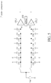
- FIGs. 4-12 are diagrams illustrating steps of the SAR ADC 100 for generating an 8-bit output signal Dout according to one embodiment.
- the SAR ADC 100 has a single-end design, that is the first/second reference signal used by the comparator 120_1/120_2 is a fixed voltage.
- the capacitor array 110_1 comprises eight capacitors C0-C7
- the capacitor array 110_2 comprises eight capacitors C0'-C7'
- the output signal Dout comprises bits B0-B7 or B0'-B7', wherein each of the bits B0 and B0' corresponds to a most significant bit (MSB), and each of the bits B7 and B7'corresponds to a least significant bit (LSB) .
- MSB most significant bit
- LSB least significant bit
- the switches SWO-SWn, the common voltage Vcm, the positive voltage V+ and the negative voltage V- are omitted here, and the bit value is used to represent the connection of the corresponding capacitor. For example, if the bit B0 shows “0”, it means that the capacitor C0 is connected to the common voltage Vcm via the switch; if the bit B0 shows "1”, it means that the capacitor C0 is connected to the positive voltage V+ via the switch; and if the bit B0 shows "-1", it means that the capacitor C0 is connected to the negative voltage V- via the switch.
- FIG. 4 also indicates that the SAR ADC 100 are sampling the input signal Vin, and the bits B0-B7 and B0'-B7' are reset to the common voltage Vcm when the sampling operations are performed.
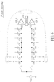
- FIG. 5 shows a comparison step of a first cycle according to one embodiment of the present invention.
- the control circuit 140 controls the capacitor array 110_1 and 110_2 to make the capacitors C0, C1, C0' and C1' connect to the common voltage Vcm, and the comparator 120_1 compares the first signal V1 with the first reference signal to generate the first comparison result, and the comparator 120_2 compares the second signal V2 with the second reference signal to generate the second comparison result.
- the first signal V1 is greater than the first reference signal
- the second signal V2 is greater than the second reference signal, so both the first comparison result and the second comparison result are equal to "1".
- FIG. 6 shows a switching step of the first cycle according to one embodiment of the present invention.
- the control circuit 140 refers to the first comparison result and the second comparison result to switch the connections of the capacitors C0, C1, C0' and C1'.
- the bits B0 and B0' are changed from “0" to "1", that is the capacitors C0 and C0' are connected to the positive voltage V+.
- the arbitration result may not be considered. In other word, no matter the generation time of the first comparison result is earlier or later than the generation time of the second comparison result, the switching step will be the same.
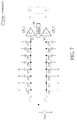
- FIG. 7 shows a comparison step of a second cycle according to one embodiment of the present invention.
- the control circuit 140 controls the capacitor array 110_1 and 110_2 to make the capacitors C2, C3, C2' and C3' connect to the common voltage Vcm, and the comparator 120_1 compares the first signal V1 with the first reference signal to generate the first comparison result, and the comparator 120_2 compares the second signal V2 with the second reference signal to generate the second comparison result.
- the first signal V1 is greater than the first reference signal
- the second signal V2 is greater than the second reference signal, so both the first comparison result and the second comparison result are equal to "1".
- FIG. 8 shows a switching step of the second cycle according to one embodiment of the present invention.
- the control circuit 140 refers to the first comparison result and the second comparison result to switch the connections of the capacitors C2, C3, C2' and C3', and further to switch the connection of one of the capacitor C1 and C1' to correct the bit value.
- the second comparison result is equal to "1”
- the bits B2 and B2' are changed from “0" to "1"
- that is the capacitors C2 and C2' are connected to the positive voltage V+.
- the bits B3 and B3' are determined by guessing to have "-1 and "1", respectively.
- the bit B1 is corrected by using the bit B1' to have the value "1".
- the arbitration result may not be considered. In other word, no matter the generation time of the first comparison result is earlier or later than the generation time of the second comparison result, the switching step will be the same.
- FIG. 9 shows a comparison step of a third cycle according to one embodiment of the present invention.
- the control circuit 140 controls the capacitor array 110_1 and 110_2 to make the capacitors C4, C5, C4' and C5' connect to the common voltage Vcm, and the comparator 120_1 compares the first signal V1 with the first reference signal to generate the first comparison result, and the comparator 120_2 compares the second signal V2 with the second reference signal to generate the second comparison result.
- the first signal V1 is greater than the first reference signal
- the second signal V2 is less than the second reference signal, so both the first comparison result and the second comparison result are equal to "1" and "-1", respectively.
- the arbitration result needs to be considered.
- the arbiter 130 generates the arbitration result "-1", which indicates that the generation time of the first comparison result is later than the generation time of the second comparison result.
- FIG. 10 shows a switching step of the third cycle according to one embodiment of the present invention.
- the control circuit 140 can determine that the first comparison result is correct or more reliable, and the control circuit 140 refers to the first comparison result to switch the connections of the capacitors C4, C5, C4' and C5', and further to switch the connection of one of the capacitor C3 and C3' to correct the bit value.
- the bits B4 and B4' are changed from "0" to "1", that is the capacitors C4 and C4' are connected to the positive voltage V+.
- the bits B5 and B5' are determined by guessing to have "-1 and "1", respectively.
- the bit B3' is corrected by using the bit B3 to have the value "-1".
- FIG. 11 shows a comparison step of a fourth cycle according to one embodiment of the present invention.
- the control circuit 140 controls the capacitor array 110_1 and 110_2 to make the capacitors C7, C8, C7' and C8' connect to the common voltage Vcm, and the comparator 120_1 compares the first signal V1 with the first reference signal to generate the first comparison result, and the comparator 120_2 compares the second signal V2 with the second reference signal to generate the second comparison result.
- the first signal V1 is greater than the first reference signal
- the second signal V2 is less than the second reference signal, so both the first comparison result and the second comparison result are equal to "1" and "-1", respectively.
- the arbitration result needs to be considered. In this embodiment, it is assumed that the arbiter 130 generates the arbitration result "1", which indicates that the generation time of the first comparison result is earlier than the generation time of the second comparison result.
- FIG. 12 shows a switching step of the fourth cycle according to one embodiment of the present invention.
- the control circuit 140 can determine that the second comparison result is correct or more reliable, and the control circuit 140 refers to the second comparison result to switch the connections of the capacitors C6, C7, C6' and C7', and further to switch the connection of one of the capacitor C5 and C5' to correct the bit value.
- the bits B6 and B6' are changed from "0" to "1", that is the capacitors C6 and C6' are connected to the positive voltage V+.
- the bits B7 and B7' are determined by guessing to have "1 and "-1", respectively.
- the bit B5 is corrected by using the bit B5' to have the value "1".
- one additional comparison may be required to determine the guesses of the bits B7 and B7'.
- the output signal Dout can be successfully generated by using the SAR ADC 100 having only two capacitors 120_1 and 120_2 and two corresponding capacitor arrays 110_1 and 110_2. Therefore, compared with the conventional 2-bit-per-cycle SAR ADC having three capacitors and three capacitor arrays, the mismatch/offset between the capacitor arrays and the comparators of the SAR ADC 100 of the present invention can be mitigated. In addition, because the arbiter design is simpler than the comparator, the SAR ADC 100 may have lower manufacturing cost.
Landscapes
- Engineering & Computer Science (AREA)
- Theoretical Computer Science (AREA)
- Analogue/Digital Conversion (AREA)
Abstract
Description
- This application claims the priority of
US Provisional Application No. 62/544,934, filed on August 14th, 2017 - In a conventional 2-bit-per-cycle SAR ADC, three capacitor arrays and three comparators are required to determine two bits in every cycle. However, because of the mismatch/offset between the capacitor arrays and the comparators, the calibrations are mandatory to prevent the performance degradation of the SAR ADC. The complexity and difficulty of the calibrations are related to the numbers of the capacitor arrays and the comparators, and the calibrations are easier if less capacitor arrays and the comparators are used. Therefore, how to provide a novel SAR ADC design with less capacitor arrays and the comparators is an important topic.
- It is therefore an objective of the present invention to provide a SAR ADC having only two capacitor arrays and two comparators, to mitigate the mismatch/offset between the capacitor arrays and the comparators and to lower the complexity of calibrations, to solve the above-mentioned problem.
- According to one embodiment of the present invention, a SAR ADC comprises a first capacitor array, a first comparator, a second capacitor array, a second comparator, an arbiter and a control circuit. The first capacitor array is arranged for receiving an input signal to generate a first signal. The first comparator is coupled to the first capacitor array, and is arranged for comparing the first signal with a first reference signal to generate a first comparison result. The second capacitor array is arranged for receiving the input signal to generate a second signal. The second comparator is coupled to the second capacitor array, and is arranged for comparing the second signal with a second reference signal to generate a second comparison result. The arbiter is coupled to the first comparator and the second comparator, and is arranged for generating an arbitration result according to the first comparison result and the second comparison result. The control circuit is coupled to the first comparator, the second comparator and the arbiter, and is arranged for generating an output signal according to the first comparison result, the second comparison result and the arbitration result.
- According to another embodiment of the present invention, a method for controlling a SAR ADC is provided, wherein the SAR ADC comprises a first capacitor array, a first comparator, a second capacitor array and a second comparator. The first capacitor array is arranged for receiving an input signal to generate a first signal. The first comparator is coupled to the first capacitor array, and is arranged for comparing the first signal with a first reference signal to generate a first comparison result. The second capacitor array is arranged for receiving the input signal to generate a second signal. The second comparator is coupled to the second capacitor array, and is arranged for comparing the second signal with a second reference signal to generate a second comparison result. In addition, the method comprises: generating an arbitration result according to the first comparison result and the second comparison result; and generating an output signal according to the first comparison result, the second comparison result and the arbitration result.
- These and other objectives of the present invention will no doubt become obvious to those of ordinary skill in the art after reading the following detailed description of the preferred embodiment that is illustrated in the various figures and drawings.
-
-
FIG. 1 is a diagram illustrating a SAR ADC according to one embodiment of the present invention. -
FIG. 2 shows that the arbiter generates the arbitration result by referring to the generation times of the first comparison result and the second comparison result according to one embodiment of the present invention. -
FIG. 3 shows the arbiter according to one embodiment of the present invention. -
FIGs. 4-12 are diagrams illustrating steps of the SAR ADC for generating an 8-bit output signal according to one embodiment. - Certain terms are used throughout the following description and claims to refer to particular system components. As one skilled in the art will appreciate, manufacturers may refer to a component by different names. This document does not intend to distinguish between components that differ in name but not function. In the following discussion and in the claims, the terms "including" and "comprising" are used in an open-ended fashion, and thus should be interpreted to mean "including, but not limited to ...". The terms "couple" and "couples" are intended to mean either an indirect or a direct electrical connection. Thus, if a first device couples to a second device, that connection may be through a direct electrical connection, or through an indirect electrical connection via other devices and connections.
-
FIG. 1 is a diagram illustrating a successive approximation register analog-to-digital converter (SAR ADC) 100 according to one embodiment of the present invention. As shown inFIG. 1 , the SAR ADC 100 comprises two capacitor arrays 110_1 and 110_2, two comparators 120_1 and 120_2, anarbiter 130 and acontrol circuit 140. In this embodiment, each of the capacitor arrays 110_1 and 110_2 comprises a plurality of capacitors C0-Cn, wherein one terminal of each of the capacitors C0-Cn of the capacitor arrays 110_1 is coupled to one input terminal of the comparator 120_1, one terminal of each of the capacitors C0-Cn of the capacitor arrays 110_2 is coupled to one input terminal of the comparator 120_2, and the other terminal of each of the capacitors C0-Cn of the capacitor arrays 110_1 and 110_2 is coupled to a common voltage Vcm, a positive voltage V+ or a negative voltage V- via a corresponding switch SWO-SWn, wherein the common voltage Vcm is an average of the positive voltage V+ and the negative voltage V-. - In this embodiment, the SAR
ADC 100 is a 2-bit-per-cycle SAR ADC, that is theSAR ADC 100 generates two bits in every cycle, wherein each cycle comprises a comparison step and a switching step, wherein the comparison step means that each of the comparators 120_1 and 120_2 generates one comparison result, and the switching step means that thecontrol circuit 140 controls a portion of the switches SWO-SWn according to the comparison result. For example, if the SARADC 100 generates an output signal Dout with 8 bits, the SARADC 100 needs four cycles to successfully generates the output signal Dout. - In the operations of the
SAR ADC 100, firstly, the switches SWn-Sw0 are controlled by control signals Vc generated by thecontrol circuit 140 to make the capacitors Cn-C0 connect to one of the common voltage Vcm, the positive voltage V+ and the negative voltage V-, and the capacitor array 110_1 samples the input signal Vin to generate a first signal V1 to the comparator 120_1, and the comparator 120_1 compares the first signal V1 with a first reference signal Vref1 to generate a first comparison result, wherein the first reference signal Vref1 may be a fixed voltage in a single-end SAR ADC design or the first reference signal Vref1 may be generated by another capacitor array in a differential design. Meanwhile, the capacitor array 110_2 samples the input signal Vin to generate a second signal V2 to the comparator 120_2, and the comparator 120_2 compares the second signal V2 with a second reference signal Vref2 to generate a second comparison result, wherein the second reference signal Vref2 may be a fixed voltage in a single-end SAR ADC design or the second reference signal Vref2 may be generated by another capacitor array in a differential design. Then, thearbiter 130 receives the first comparison result and the second comparison result and generates an arbitration result according to the first comparison result and the second comparison result, wherein the arbitration result indicates which of the first reference signal Vref1 or the second reference signal Vref2 is more close to the target. Then, thecontrol circuit 140 generates two bits of the output signal Dout by referring to the first comparison result, the second comparison result and the arbitration result. Specifically, the settings of the first reference signal Vref1 and the second reference signal Vref2 can be used to determine which range the sampled signal belongs to, and the arbitration result provides auxiliary information for determining which one of the first reference signal Vref1 and the second reference signal Vref2 is closer to the sampled signal, and the two bits of the output signal Dout can be determined accordingly. For example, if the first comparison result and the second comparison result are inconsistent (e.g. the first comparison result is "0" while the second comparison result is "1"), thearbiter 130 may receive the first comparison result and the second comparison result to generate the arbitration result according to their generation information, wherein the generation information may be generation time of the first/second comparison results. - In one embodiment, the
arbiter 130 is a time-based arbiter, and thearbiter 130 receives the first comparison result and the second comparison result to generate the arbitration result by referring to the generation times of the first comparison result and the second comparison result (i.e. the time points that the first comparison result and the second comparison result are successfully outputted) . Specifically, because the processing speed of the comparator 110_1/110_2 depends on a residue between the sampled signal and the reference signal (i.e. , a difference between the first/second signal V1/V2 and the first/second reference signal), that is when the first signal V1 is closer to the first reference signal Vref1, the comparator 110_1 needs more time to generate the first comparison result. Therefore, when the generation time of the first comparator result is later than the generation time of the second comparison result, it means that the first comparison result is closer to the goal voltage (i.e. the first reference signal Vref1), and thearbiter 130 may generate the arbitration result indicating that the first comparison result is correct or more reliable; on the other hand, when the generation time of the first comparator result is earlier than the generation time of the second comparison result, it means that the second comparison result is closer to the goal voltage (i.e. the second reference signal Vref2), and thearbiter 130 may generate the arbitration result indicating that the second comparison result is correct or more reliable. -
FIG. 2 shows that thearbiter 130 generates the arbitration result by referring to the generation times of the first comparison result and the second comparison result according to one embodiment of the present invention. As shown inFIG. 2 , in addition to the first comparison result, the comparator 120_1 further generates a first valid signal Valid_1 for indicating the generation time of the first comparison result. In detail, when the comparator 120_1 completes the comparing operation and successfully outputs the first comparison result, the first valid signal Valid_1 changes its voltage level or logical value, such as from a low voltage level (i.e. logical value "0") to a high voltage level (i.e. logical value "1"). Similarly, when the comparator 120_2 completes the comparing operation and successfully outputs the second comparison result, the second valid signal Valid_2 changes its voltage level or logical value, such as from a low voltage level (i.e. logical value "0") to a high voltage level (i.e. logical value "1") . Therefore, thearbiter 130 can refer to transition times of the first valid signal Valid_1 and the second valid signal Valid_2 to determine the generation times of the first comparison result and the second comparison result, then thearbiter 130 generates the arbitration result indicating which one of the first comparison result and second comparison result has a later or earlier generation time. -
FIG. 3 shows thearbiter 130 according to one embodiment of the present invention, where thearbiter 130 is implemented by a set-reset latch (SR latch) having two NAND gates for receiving the first valid signal Valid_1 and the second valid signal Valid_2. As shown inFIG. 3 , there are two scenarios, where the first scenario indicates that the generation time of the first comparison result is earlier than the generation time of the second comparison result, and the second scenario indicates that the generation time of the first comparison result is later than the generation time of the second comparison result. For the first scenario, in the preset state, the comparators 120_1 and 120_2 does not generate the first comparison result and the second comparison result, respectively, so the first valid signal Valid_1 and the second valid signal Valid_2 (i.e., "S" node and "R" node of the SR latch) correspond to logical value "0". Then, the comparator 120_1 successfully generates the first comparison result, and the first valid signal Valid_1 changes its logical value, and a "Qb" node of the SR latch becomes logical value "0" while a "Q" node of the SR latch stays in the logical value "1". Then, the comparator 120_2 successfully generates the second comparison result, and the second valid signal Valid_2 changes its logical value, and the "Q" node and the "Qb" node of the SR latch remain the same. Therefore, in the final state, the "Q" node and the "Qb" node of the SR latch correspond to the logical values "1" and "0", respectively, and this logical value combination serves as the arbitration result indicating that the generation time of the first comparison result is earlier than the generation time of the second comparison result. - For the second scenario, in the preset state, the comparators 120_1 and 120_2 does not generate the first comparison result and the second comparison result, respectively, so the first valid signal Valid_1 and the second valid signal Valid_2 correspond to logical value "0". Then, the comparator 120_2 successfully generates the second comparison result, and the second valid signal Valid_1 changes its logical value, and the "Q" node of the SR latch becomes logical value "0" while the "Qb" node of the SR latch stays in the logical value "1". Then, the comparator 120_1 successfully generates the first comparison result, and the first valid signal Valid_1 changes its logical value, and the "Q" node and the "Qb" node of the SR latch remain the same. Therefore, in the final state, the "Q" node and the "Qb" node of the SR latch correspond to the logical values "0" and "1", respectively, and this logical value combination serves as the arbitration result indicating that the generation time of the first comparison result is later than the generation time of the second comparison result.
- It is noted that the embodiment shown in
FIG. 2 and3 is for illustrative purposes only, without a limitation of the present invention. As long as thearbiter 130 can generate the arbitration result indicating that which one of the first comparison result and the second comparison result has a later generation time, the arbiter may have different circuit designs. - In the following embodiment, without a limitation of the present invention, the value at the "Q" node of the SR latch serves as the arbitration result. That is, the
arbiter 130 generates the arbitration result "1" to thecontrol circuit 140 if the generation time of the first comparison result is earlier than the generation time of the second comparison result; and thearbiter 130 generates the arbitration result "0" (or "-1" with the same meaning in the following embodiment) to thecontrol circuit 140 if the generation time of the first comparison result is later than the generation time of the second comparison result. -
FIGs. 4-12 are diagrams illustrating steps of theSAR ADC 100 for generating an 8-bit output signal Dout according to one embodiment. To make the example be simpler, theSAR ADC 100 has a single-end design, that is the first/second reference signal used by the comparator 120_1/120_2 is a fixed voltage. As shown inFIG. 4 , the capacitor array 110_1 comprises eight capacitors C0-C7, and the capacitor array 110_2 comprises eight capacitors C0'-C7', the output signal Dout comprises bits B0-B7 or B0'-B7', wherein each of the bits B0 and B0' corresponds to a most significant bit (MSB), and each of the bits B7 and B7'corresponds to a least significant bit (LSB) . For simplicity, the switches SWO-SWn, the common voltage Vcm, the positive voltage V+ and the negative voltage V- are omitted here, and the bit value is used to represent the connection of the corresponding capacitor. For example, if the bit B0 shows "0", it means that the capacitor C0 is connected to the common voltage Vcm via the switch; if the bit B0 shows "1", it means that the capacitor C0 is connected to the positive voltage V+ via the switch; and if the bit B0 shows "-1", it means that the capacitor C0 is connected to the negative voltage V- via the switch. - In addition, the embodiment shown in
FIG. 4 also indicates that theSAR ADC 100 are sampling the input signal Vin, and the bits B0-B7 and B0'-B7' are reset to the common voltage Vcm when the sampling operations are performed. -
FIG. 5 shows a comparison step of a first cycle according to one embodiment of the present invention. As shown inFIG. 5 , thecontrol circuit 140 controls the capacitor array 110_1 and 110_2 to make the capacitors C0, C1, C0' and C1' connect to the common voltage Vcm, and the comparator 120_1 compares the first signal V1 with the first reference signal to generate the first comparison result, and the comparator 120_2 compares the second signal V2 with the second reference signal to generate the second comparison result. In this embodiment, it is assumed that the first signal V1 is greater than the first reference signal, and the second signal V2 is greater than the second reference signal, so both the first comparison result and the second comparison result are equal to "1". -
FIG. 6 shows a switching step of the first cycle according to one embodiment of the present invention. As shown inFIG. 6 , thecontrol circuit 140 refers to the first comparison result and the second comparison result to switch the connections of the capacitors C0, C1, C0' and C1'. Specifically, because both the first comparison result and the second comparison result are equal to "1", the bits B0 and B0' are changed from "0" to "1", that is the capacitors C0 and C0' are connected to the positive voltage V+. In addition, the bit B1 is determined by a conservative guessing and the bit B1 is an inverse of the bit B0 (i.e. B1="-1"), and the bit B1' is determined by an aggressive guessing and the bit B1' is the same as the bit B0' (i.e. B1'="1"). - In addition, because the first comparison result is the same as the second comparison result in the first cycle, the arbitration result may not be considered. In other word, no matter the generation time of the first comparison result is earlier or later than the generation time of the second comparison result, the switching step will be the same.
-
FIG. 7 shows a comparison step of a second cycle according to one embodiment of the present invention. As shown inFIG. 7 , thecontrol circuit 140 controls the capacitor array 110_1 and 110_2 to make the capacitors C2, C3, C2' and C3' connect to the common voltage Vcm, and the comparator 120_1 compares the first signal V1 with the first reference signal to generate the first comparison result, and the comparator 120_2 compares the second signal V2 with the second reference signal to generate the second comparison result. In this embodiment, it is assumed that the first signal V1 is greater than the first reference signal, and the second signal V2 is greater than the second reference signal, so both the first comparison result and the second comparison result are equal to "1". -
FIG. 8 shows a switching step of the second cycle according to one embodiment of the present invention. As shown inFIG. 8 , thecontrol circuit 140 refers to the first comparison result and the second comparison result to switch the connections of the capacitors C2, C3, C2' and C3', and further to switch the connection of one of the capacitor C1 and C1' to correct the bit value. Specifically, because the second comparison result is equal to "1", the bits B2 and B2' are changed from "0" to "1", that is the capacitors C2 and C2' are connected to the positive voltage V+. The bits B3 and B3' are determined by guessing to have "-1 and "1", respectively. In addition, the bit B1 is corrected by using the bit B1' to have the value "1". - In addition, because the first comparison result is the same as the second comparison result in the second cycle, the arbitration result may not be considered. In other word, no matter the generation time of the first comparison result is earlier or later than the generation time of the second comparison result, the switching step will be the same.
-
FIG. 9 shows a comparison step of a third cycle according to one embodiment of the present invention. As shown inFIG. 9 , thecontrol circuit 140 controls the capacitor array 110_1 and 110_2 to make the capacitors C4, C5, C4' and C5' connect to the common voltage Vcm, and the comparator 120_1 compares the first signal V1 with the first reference signal to generate the first comparison result, and the comparator 120_2 compares the second signal V2 with the second reference signal to generate the second comparison result. In this embodiment, it is assumed that the first signal V1 is greater than the first reference signal, and the second signal V2 is less than the second reference signal, so both the first comparison result and the second comparison result are equal to "1" and "-1", respectively. In addition, because the first comparison result and the second comparison result are inconsistent, the arbitration result needs to be considered. In this embodiment, it is assumed that thearbiter 130 generates the arbitration result "-1", which indicates that the generation time of the first comparison result is later than the generation time of the second comparison result. -
FIG. 10 shows a switching step of the third cycle according to one embodiment of the present invention. As shown inFIG. 10 , because thearbiter 130 generates the arbitration result indicating that the generation time of the first comparison result is later than the generation time of the second comparison result, thecontrol circuit 140 can determine that the first comparison result is correct or more reliable, and thecontrol circuit 140 refers to the first comparison result to switch the connections of the capacitors C4, C5, C4' and C5', and further to switch the connection of one of the capacitor C3 and C3' to correct the bit value. Specifically, because the first comparison result is determined to be correct, the bits B4 and B4' are changed from "0" to "1", that is the capacitors C4 and C4' are connected to the positive voltage V+. The bits B5 and B5' are determined by guessing to have "-1 and "1", respectively. In addition, the bit B3' is corrected by using the bit B3 to have the value "-1". -
FIG. 11 shows a comparison step of a fourth cycle according to one embodiment of the present invention. As shown inFIG. 11 , thecontrol circuit 140 controls the capacitor array 110_1 and 110_2 to make the capacitors C7, C8, C7' and C8' connect to the common voltage Vcm, and the comparator 120_1 compares the first signal V1 with the first reference signal to generate the first comparison result, and the comparator 120_2 compares the second signal V2 with the second reference signal to generate the second comparison result. In this embodiment, it is assumed that the first signal V1 is greater than the first reference signal, and the second signal V2 is less than the second reference signal, so both the first comparison result and the second comparison result are equal to "1" and "-1", respectively. In addition, because the first comparison result and the second comparison result are inconsistent, the arbitration result needs to be considered. In this embodiment, it is assumed that thearbiter 130 generates the arbitration result "1", which indicates that the generation time of the first comparison result is earlier than the generation time of the second comparison result. -
FIG. 12 shows a switching step of the fourth cycle according to one embodiment of the present invention. As shown inFIG. 12 , because thearbiter 130 generates the arbitration result indicating that the generation time of the first comparison result is earlier than the generation time of the second comparison result, thecontrol circuit 140 can determine that the second comparison result is correct or more reliable, and thecontrol circuit 140 refers to the second comparison result to switch the connections of the capacitors C6, C7, C6' and C7', and further to switch the connection of one of the capacitor C5 and C5' to correct the bit value. Specifically, because the second comparison result is determined to be correct, the bits B6 and B6' are changed from "0" to "1", that is the capacitors C6 and C6' are connected to the positive voltage V+. The bits B7 and B7' are determined by guessing to have "1 and "-1", respectively. In addition, the bit B5 is corrected by using the bit B5' to have the value "1". - In addition, one additional comparison may be required to determine the guesses of the bits B7 and B7'.
- By using the aforementioned embodiment, the output signal Dout can be successfully generated by using the
SAR ADC 100 having only two capacitors 120_1 and 120_2 and two corresponding capacitor arrays 110_1 and 110_2. Therefore, compared with the conventional 2-bit-per-cycle SAR ADC having three capacitors and three capacitor arrays, the mismatch/offset between the capacitor arrays and the comparators of theSAR ADC 100 of the present invention can be mitigated. In addition, because the arbiter design is simpler than the comparator, theSAR ADC 100 may have lower manufacturing cost. - Those skilled in the art will readily observe that numerous modifications and alterations of the device and method may be made while retaining the teachings of the invention. Accordingly, the above disclosure should be construed as limited only by the metes and bounds of the appended claims.
Claims (14)
- A successive approximation register analog-to-digital converter, SAR ADC, (100) comprising:a first capacitor array, for receiving an input signal to generate a first signal;a first comparator, coupled to the first capacitor array, for comparing the first signal with a first reference signal to generate a first comparison result;a second capacitor array, for receiving the input signal to generate a second signal;a second comparator, coupled to the second capacitor array, for comparing the second signal with a second reference signal to generate a second comparison result;an arbiter (130), coupled to the first comparator and the second comparator, for receiving the first comparison result and the second comparison result, and generating an arbitration result according to the first comparison result and the second comparison result; anda control circuit (140), coupled to the first comparator, the second comparator and the arbiter (130), for generating an output signal according to the first comparison result, the second comparison result and the arbitration result.
- The SAR ADC (100) of claim 1, wherein the SAR ADC (100) is a 2-bit-per-cycle SAR ADC.
- The SAR ADC (100) of claim 2, wherein the SAR ADC (100) does not have any other comparator for receiving a signal generated by a capacitor array processing the input signal.
- The SAR ADC (100) of claim 1, wherein the arbiter (130) is a time-based arbiter.
- The SAR ADC (100) of claim 4, wherein the arbiter (130) generates the arbitration result by referring generation times of the first comparison result and the second comparison result.
- The SAR ADC (100) of claim 5, wherein when the generation time of the first comparison result is later than the generation time of the second comparison result, the arbiter (130) generates that arbitration result indicating that the first comparison result is correct, and the control circuit (140) uses the first comparison result to generate the output signal if the first comparison result and the second comparison result are inconsistent; and when the generation time of the first comparison result is earlier than the generation time of the second comparison result, the arbiter (130) generates that arbitration result indicating that the second comparison result is correct, and the control circuit (140) uses the second comparison result to generate the output signal if the first comparison result and the second comparison result are inconsistent.
- The SAR ADC (100) of claim 5, wherein the first comparator further generates a first valid signal for indicating the generation time of the first comparison result, the second comparator further generates a second valid signal for indicating the generation time of the second comparison result, and the arbiter (130) refers to the first valid signal and the second valid signal to generate the arbitration result.
- The SAR ADC (100) of claim 5, wherein the arbiter (130) is a set-reset, SR, latch.
- A method for controlling a successive approximation register analog-to-digital converter, SAR ADC, (100) wherein the SAR ADC (100) comprises:a first capacitor array, for receiving an input signal to generate a first signal;a first comparator, coupled to the first capacitor array, for comparing the first signal with a first reference signal to generate a first comparison result;a second capacitor array, for receiving the input signal to generate a second signal;a second comparator, coupled to the second capacitor array, for comparing the second signal with a second reference signal to generate a second comparison result; andthe method comprises:receiving the first comparison result and the second comparison result, and generating an arbitration result according to the first comparison result and the second comparison result; andgenerating an output signal according to the first comparison result, the second comparison result and the arbitration result.
- The method of claim 9, wherein the SAR ADC (100) is a 2-bit-per-cycle SAR ADC.
- The method of claim 9, wherein the step of generating the arbitration result according to the first comparison result and the second comparison result comprises:using a time-based arbiter to generate the arbitration result.
- The method of claim 11, wherein the time-based arbiter is a set-reset, SR, latch.
- The method of claim 9, wherein the step of generating the arbitration result according to the first comparison result and the second comparison result comprises:referring to generation times of the first comparison result and the second comparison result to generate the arbitration result.
- The method of claim 13, wherein the step of j generating the arbitration result according to the first comparison result and the second comparison result c, and the step of generating the output signal according to the first comparison result, the second comparison result and the arbitration result comprise:when the generation time of the first comparison result is later than the generation time of the second comparison result, generating the arbitration result indicating that the first comparison result is correct, and using the first comparison result to generate the output signal if the first comparison result and the second comparison result are inconsistent; andwhen the generation time of the first comparison result is earlier than the generation time of the second comparison result, generating the arbitration result indicating that the second comparison result is correct, and using the second comparison result to generate the output signal if the first comparison result and the second comparison result are inconsistent.
Applications Claiming Priority (2)
| Application Number | Priority Date | Filing Date | Title |
|---|---|---|---|
| US201762544934P | 2017-08-14 | 2017-08-14 | |
| US16/043,180 US10574248B2 (en) | 2017-08-14 | 2018-07-24 | Successive approximation register analog-to-digital converter and associated control method |
Publications (1)
| Publication Number | Publication Date |
|---|---|
| EP3444951A1 true EP3444951A1 (en) | 2019-02-20 |
Family
ID=63144869
Family Applications (1)
| Application Number | Title | Priority Date | Filing Date |
|---|---|---|---|
| EP18187205.2A Ceased EP3444951A1 (en) | 2017-08-14 | 2018-08-03 | Successive approximation register analog-to-digital converter and associated control method |
Country Status (4)
| Country | Link |
|---|---|
| US (1) | US10574248B2 (en) |
| EP (1) | EP3444951A1 (en) |
| CN (1) | CN109391269B (en) |
| TW (1) | TWI674764B (en) |
Families Citing this family (3)
| Publication number | Priority date | Publication date | Assignee | Title |
|---|---|---|---|---|
| CN111431535B (en) * | 2020-04-22 | 2023-05-12 | 电子科技大学 | A 2b/cycle successive approximation analog-to-digital converter and its quantization method |
| CN111711453B (en) * | 2020-08-19 | 2020-11-13 | 微龛(广州)半导体有限公司 | Successive approximation type analog-to-digital converter |
| CN112600540B (en) * | 2021-03-04 | 2021-05-14 | 上海南芯半导体科技有限公司 | A high-precision comparator suitable for current demodulation in wireless charging |
Citations (1)
| Publication number | Priority date | Publication date | Assignee | Title |
|---|---|---|---|---|
| US5920275A (en) * | 1996-09-09 | 1999-07-06 | Iowa State University Research Foundation, Inc. | Analog-to-digital converter using weighted capacitor array and interpolating comparator |
Family Cites Families (15)
| Publication number | Priority date | Publication date | Assignee | Title |
|---|---|---|---|---|
| US5646651A (en) | 1994-12-14 | 1997-07-08 | Spannaus; John | Block mode, multiple access multi-media/graphics memory |
| US5621409A (en) | 1995-02-15 | 1997-04-15 | Analog Devices, Inc. | Analog-to-digital conversion with multiple charge balance conversions |
| US6956520B2 (en) * | 2003-06-03 | 2005-10-18 | Silicon Labs Cp, Inc. | SAR data converter with unequal clock pulses for MSBS to allow for settling |
| US7205921B1 (en) * | 2006-03-27 | 2007-04-17 | Intel Corporation | Hybrid analog-to-digital converter |
| FR2907986B1 (en) * | 2006-10-26 | 2009-02-27 | Atmel Nantes Sa Sa | SUCCESSIVE APPROXIMATE ANALOGUE / DIGITAL CONVERTER, INTEGRATED COMPONENT AND CORRESPONDING CONVERSION METHOD. |
| US7737875B2 (en) * | 2007-12-13 | 2010-06-15 | Nxp B.V. | Time interpolation flash ADC having automatic feedback calibration |
| JP2010199798A (en) * | 2009-02-24 | 2010-09-09 | Renesas Electronics Corp | Analog/digital conversion circuit |
| US8223044B2 (en) * | 2010-04-22 | 2012-07-17 | Texas Instruments Incorporated | INL correction circuitry and method for SAR ADC |
| CN102790618A (en) * | 2011-05-18 | 2012-11-21 | 财团法人成大研究发展基金会 | Successively-approximating analogue/digital converter with window predicting function and method |
| US8806316B2 (en) * | 2012-01-11 | 2014-08-12 | Micron Technology, Inc. | Circuits, integrated circuits, and methods for interleaved parity computation |
| JP6120495B2 (en) * | 2012-06-04 | 2017-04-26 | キヤノン株式会社 | Imaging device, driving method of imaging device, imaging system, and driving method of imaging system |
| JP6102521B2 (en) * | 2013-05-29 | 2017-03-29 | 株式会社ソシオネクスト | SAR analog-digital conversion method and SAR analog-digital conversion circuit |
| US9148159B1 (en) * | 2014-03-13 | 2015-09-29 | Texas Instruments Incorporated | Dual comparator-based error correction scheme for analog-to-digital converters |
| CN104242943A (en) * | 2014-09-29 | 2014-12-24 | 清华大学 | Six-bit asynchronous successive approximation analog-digital converter based on resistor type digital-analog converter |
| US10128862B2 (en) * | 2016-01-21 | 2018-11-13 | Mediatek Inc. | Successive approximation register analog-to-digital converter applying calibration circuit, associated calibrating method, and associated electronic device |
-
2018
- 2018-07-24 US US16/043,180 patent/US10574248B2/en active Active
- 2018-08-03 EP EP18187205.2A patent/EP3444951A1/en not_active Ceased
- 2018-08-14 CN CN201810924918.3A patent/CN109391269B/en active Active
- 2018-08-14 TW TW107128300A patent/TWI674764B/en active
Patent Citations (1)
| Publication number | Priority date | Publication date | Assignee | Title |
|---|---|---|---|---|
| US5920275A (en) * | 1996-09-09 | 1999-07-06 | Iowa State University Research Foundation, Inc. | Analog-to-digital converter using weighted capacitor array and interpolating comparator |
Non-Patent Citations (3)
| Title |
|---|
| CHAN CHI-HANG ET AL: "26.5 A 5.5mW 6b 5GS/S 4-lnterleaved 3b/cycle SAR ADC in 65nm CMOS", 2015 IEEE INTERNATIONAL SOLID-STATE CIRCUITS CONFERENCE - (ISSCC) DIGEST OF TECHNICAL PAPERS, IEEE, 22 February 2015 (2015-02-22), pages 1 - 3, XP032748236, ISBN: 978-1-4799-6223-5, [retrieved on 20150317], DOI: 10.1109/ISSCC.2015.7063128 * |
| HUALING WU ET AL: "A novel 10bit 90MS/s 2b/cycle SAR ADC", 2015 INTERNATIONAL CONFERENCE ON ADVANCED TECHNOLOGIES FOR COMMUNICATIONS (ATC), October 2013 (2013-10-01), pages 521 - 524, XP055539188, ISSN: 2162-1020, ISBN: 978-1-4673-8372-1, DOI: 10.1109/ATC.2013.6698170 * |
| YUN-SHIANG SHU: "A 6b 3GS/s 11mW fully dynamic flash ADC in 40nm CMOS with reduced number of comparators", VLSI CIRCUITS (VLSIC), 2012 SYMPOSIUM ON, IEEE, 13 June 2012 (2012-06-13), pages 26 - 27, XP032204378, ISBN: 978-1-4673-0848-9, DOI: 10.1109/VLSIC.2012.6243772 * |
Also Published As
| Publication number | Publication date |
|---|---|
| TW201911758A (en) | 2019-03-16 |
| CN109391269A (en) | 2019-02-26 |
| US20190052282A1 (en) | 2019-02-14 |
| TWI674764B (en) | 2019-10-11 |
| CN109391269B (en) | 2023-02-28 |
| US10574248B2 (en) | 2020-02-25 |
Similar Documents
| Publication | Publication Date | Title |
|---|---|---|
| US10044364B1 (en) | Metastability error correction methods and circuits for asynchronous successive approximation analog to digital converter (SAR ADC) | |
| US9432046B1 (en) | Successive approximation analog-to-digital converter | |
| US9755659B2 (en) | ASAR ADC circuit and conversion method thereof | |
| US20200228132A1 (en) | Analog-to-digital converter device | |
| US10116318B1 (en) | Method and system for asynchronous clock generation for successive approximation analog-to-digital converter (SAR ADC) | |
| US9148159B1 (en) | Dual comparator-based error correction scheme for analog-to-digital converters | |
| CN106537786A (en) | Asynchronous successive approximation register analog-to-digital converter (SAR ADC) in synchronous systems | |
| US9673832B2 (en) | Successive approximation analog-to-digital converter and accuracy improving method thereof | |
| CN103178847A (en) | Successive approximation register analog-to-digital converter and method thereof | |
| US10574248B2 (en) | Successive approximation register analog-to-digital converter and associated control method | |
| CN116455395B (en) | Successive approximation analog-to-digital conversion circuits, analog-to-digital converters and electronic equipment | |
| US10355684B2 (en) | Calculation code generation circuit and digital correction circuit including the same | |
| JP2013048366A (en) | Successive approximation ad converter and radio receiver | |
| CN104348485A (en) | Analog to digital converter and method for converting analog signals into digital signals | |
| US9685972B1 (en) | Asynchronous successive approximation register analog-to-digital converter circuit and method for configuring the same | |
| TW201924227A (en) | Method and apparatus for enabling wide input common-mode range in SAR ADCs with no additional active circuitry | |
| US7405681B2 (en) | A/D converter calibration test sequence insertion | |
| US11258454B2 (en) | Analog-digital converter | |
| CN113726339B (en) | Error feedback-based offset voltage reduction method and data converter | |
| CN115149954B (en) | Metastable state correction circuit and successive approximation type analog-to-digital conversion circuit | |
| CN105991138A (en) | Asynchronous successive approximation register analog-to-digital conversion circuit | |
| US12476647B2 (en) | Analog-to-digital converter | |
| CN113556127B (en) | Digital slope type analog-digital converter device and signal conversion method | |
| CN109428595B (en) | Continuous approximation analog-to-digital conversion correcting device | |
| US7034724B2 (en) | Training circuit and method of digital-analog converter and analog-digital converter |
Legal Events
| Date | Code | Title | Description |
|---|---|---|---|
| PUAI | Public reference made under article 153(3) epc to a published international application that has entered the european phase |
Free format text: ORIGINAL CODE: 0009012 |
|
| STAA | Information on the status of an ep patent application or granted ep patent |
Free format text: STATUS: THE APPLICATION HAS BEEN PUBLISHED |
|
| AK | Designated contracting states |
Kind code of ref document: A1 Designated state(s): AL AT BE BG CH CY CZ DE DK EE ES FI FR GB GR HR HU IE IS IT LI LT LU LV MC MK MT NL NO PL PT RO RS SE SI SK SM TR |
|
| AX | Request for extension of the european patent |
Extension state: BA ME |
|
| STAA | Information on the status of an ep patent application or granted ep patent |
Free format text: STATUS: REQUEST FOR EXAMINATION WAS MADE |
|
| 17P | Request for examination filed |
Effective date: 20190808 |
|
| RBV | Designated contracting states (corrected) |
Designated state(s): AL AT BE BG CH CY CZ DE DK EE ES FI FR GB GR HR HU IE IS IT LI LT LU LV MC MK MT NL NO PL PT RO RS SE SI SK SM TR |
|
| STAA | Information on the status of an ep patent application or granted ep patent |
Free format text: STATUS: EXAMINATION IS IN PROGRESS |
|
| 17Q | First examination report despatched |
Effective date: 20210429 |
|
| STAA | Information on the status of an ep patent application or granted ep patent |
Free format text: STATUS: THE APPLICATION HAS BEEN REFUSED |
|
| 18R | Application refused |
Effective date: 20230120 |