EP3444596A1 - Sensor board and sensor device - Google Patents
Sensor board and sensor device Download PDFInfo
- Publication number
- EP3444596A1 EP3444596A1 EP17799452.2A EP17799452A EP3444596A1 EP 3444596 A1 EP3444596 A1 EP 3444596A1 EP 17799452 A EP17799452 A EP 17799452A EP 3444596 A1 EP3444596 A1 EP 3444596A1
- Authority
- EP
- European Patent Office
- Prior art keywords
- electrode
- sensor board
- electrodes
- positive
- sensing
- Prior art date
- Legal status (The legal status is an assumption and is not a legal conclusion. Google has not performed a legal analysis and makes no representation as to the accuracy of the status listed.)
- Granted
Links
- 239000000758 substrate Substances 0.000 claims abstract description 67
- 239000010410 layer Substances 0.000 description 102
- 239000013618 particulate matter Substances 0.000 description 73
- 238000001514 detection method Methods 0.000 description 56
- 239000004071 soot Substances 0.000 description 54
- 239000007769 metal material Substances 0.000 description 25
- 238000007747 plating Methods 0.000 description 22
- 238000004519 manufacturing process Methods 0.000 description 20
- 238000005259 measurement Methods 0.000 description 19
- 238000000034 method Methods 0.000 description 15
- BASFCYQUMIYNBI-UHFFFAOYSA-N platinum Chemical compound [Pt] BASFCYQUMIYNBI-UHFFFAOYSA-N 0.000 description 14
- 239000000919 ceramic Substances 0.000 description 13
- PXHVJJICTQNCMI-UHFFFAOYSA-N Nickel Chemical compound [Ni] PXHVJJICTQNCMI-UHFFFAOYSA-N 0.000 description 12
- 239000000470 constituent Substances 0.000 description 12
- XEEYBQQBJWHFJM-UHFFFAOYSA-N Iron Chemical compound [Fe] XEEYBQQBJWHFJM-UHFFFAOYSA-N 0.000 description 10
- PCHJSUWPFVWCPO-UHFFFAOYSA-N gold Chemical compound [Au] PCHJSUWPFVWCPO-UHFFFAOYSA-N 0.000 description 10
- 229910052737 gold Inorganic materials 0.000 description 10
- 239000010931 gold Substances 0.000 description 10
- 239000000463 material Substances 0.000 description 10
- 230000003647 oxidation Effects 0.000 description 10
- 238000007254 oxidation reaction Methods 0.000 description 10
- 230000008859 change Effects 0.000 description 9
- 238000010586 diagram Methods 0.000 description 9
- 239000011521 glass Substances 0.000 description 9
- 238000009826 distribution Methods 0.000 description 8
- AMWRITDGCCNYAT-UHFFFAOYSA-L hydroxy(oxo)manganese;manganese Chemical compound [Mn].O[Mn]=O.O[Mn]=O AMWRITDGCCNYAT-UHFFFAOYSA-L 0.000 description 8
- 238000009825 accumulation Methods 0.000 description 7
- 229910052697 platinum Inorganic materials 0.000 description 7
- 229910045601 alloy Inorganic materials 0.000 description 6
- 239000000956 alloy Substances 0.000 description 6
- 230000000694 effects Effects 0.000 description 6
- 238000010304 firing Methods 0.000 description 6
- 230000006872 improvement Effects 0.000 description 6
- 229910052759 nickel Inorganic materials 0.000 description 6
- 230000035945 sensitivity Effects 0.000 description 6
- 229910000679 solder Inorganic materials 0.000 description 6
- 230000001464 adherent effect Effects 0.000 description 5
- 238000010276 construction Methods 0.000 description 5
- 239000013078 crystal Substances 0.000 description 5
- 229910052742 iron Inorganic materials 0.000 description 5
- 229910052751 metal Inorganic materials 0.000 description 5
- 239000002184 metal Substances 0.000 description 5
- TWNQGVIAIRXVLR-UHFFFAOYSA-N oxo(oxoalumanyloxy)alumane Chemical compound O=[Al]O[Al]=O TWNQGVIAIRXVLR-UHFFFAOYSA-N 0.000 description 5
- VYPSYNLAJGMNEJ-UHFFFAOYSA-N Silicium dioxide Chemical compound O=[Si]=O VYPSYNLAJGMNEJ-UHFFFAOYSA-N 0.000 description 4
- BQCADISMDOOEFD-UHFFFAOYSA-N Silver Chemical compound [Ag] BQCADISMDOOEFD-UHFFFAOYSA-N 0.000 description 4
- MCMNRKCIXSYSNV-UHFFFAOYSA-N Zirconium dioxide Chemical compound O=[Zr]=O MCMNRKCIXSYSNV-UHFFFAOYSA-N 0.000 description 4
- PNEYBMLMFCGWSK-UHFFFAOYSA-N aluminium oxide Inorganic materials [O-2].[O-2].[O-2].[Al+3].[Al+3] PNEYBMLMFCGWSK-UHFFFAOYSA-N 0.000 description 4
- 238000005219 brazing Methods 0.000 description 4
- 239000004020 conductor Substances 0.000 description 4
- 230000007797 corrosion Effects 0.000 description 4
- 238000005260 corrosion Methods 0.000 description 4
- 238000007772 electroless plating Methods 0.000 description 4
- 238000009713 electroplating Methods 0.000 description 4
- 239000011159 matrix material Substances 0.000 description 4
- 230000008569 process Effects 0.000 description 4
- 229910052709 silver Inorganic materials 0.000 description 4
- 239000004332 silver Substances 0.000 description 4
- PWHULOQIROXLJO-UHFFFAOYSA-N Manganese Chemical compound [Mn] PWHULOQIROXLJO-UHFFFAOYSA-N 0.000 description 3
- 230000008901 benefit Effects 0.000 description 3
- 238000000354 decomposition reaction Methods 0.000 description 3
- 230000003247 decreasing effect Effects 0.000 description 3
- CPLXHLVBOLITMK-UHFFFAOYSA-N magnesium oxide Inorganic materials [Mg]=O CPLXHLVBOLITMK-UHFFFAOYSA-N 0.000 description 3
- 239000000395 magnesium oxide Substances 0.000 description 3
- AXZKOIWUVFPNLO-UHFFFAOYSA-N magnesium;oxygen(2-) Chemical compound [O-2].[Mg+2] AXZKOIWUVFPNLO-UHFFFAOYSA-N 0.000 description 3
- 229910052748 manganese Inorganic materials 0.000 description 3
- 239000011572 manganese Substances 0.000 description 3
- 239000002245 particle Substances 0.000 description 3
- 239000000843 powder Substances 0.000 description 3
- 238000007639 printing Methods 0.000 description 3
- 229910052814 silicon oxide Inorganic materials 0.000 description 3
- 230000003245 working effect Effects 0.000 description 3
- 229910000531 Co alloy Inorganic materials 0.000 description 2
- RYGMFSIKBFXOCR-UHFFFAOYSA-N Copper Chemical compound [Cu] RYGMFSIKBFXOCR-UHFFFAOYSA-N 0.000 description 2
- KDLHZDBZIXYQEI-UHFFFAOYSA-N Palladium Chemical compound [Pd] KDLHZDBZIXYQEI-UHFFFAOYSA-N 0.000 description 2
- NEIHULKJZQTQKJ-UHFFFAOYSA-N [Cu].[Ag] Chemical compound [Cu].[Ag] NEIHULKJZQTQKJ-UHFFFAOYSA-N 0.000 description 2
- KGWWEXORQXHJJQ-UHFFFAOYSA-N [Fe].[Co].[Ni] Chemical compound [Fe].[Co].[Ni] KGWWEXORQXHJJQ-UHFFFAOYSA-N 0.000 description 2
- 239000011230 binding agent Substances 0.000 description 2
- 229910052804 chromium Inorganic materials 0.000 description 2
- 239000011651 chromium Substances 0.000 description 2
- 229910052802 copper Inorganic materials 0.000 description 2
- 239000010949 copper Substances 0.000 description 2
- PMHQVHHXPFUNSP-UHFFFAOYSA-M copper(1+);methylsulfanylmethane;bromide Chemical compound Br[Cu].CSC PMHQVHHXPFUNSP-UHFFFAOYSA-M 0.000 description 2
- KZHJGOXRZJKJNY-UHFFFAOYSA-N dioxosilane;oxo(oxoalumanyloxy)alumane Chemical compound O=[Si]=O.O=[Si]=O.O=[Al]O[Al]=O.O=[Al]O[Al]=O.O=[Al]O[Al]=O KZHJGOXRZJKJNY-UHFFFAOYSA-N 0.000 description 2
- 239000002241 glass-ceramic Substances 0.000 description 2
- 239000000203 mixture Substances 0.000 description 2
- 229910052863 mullite Inorganic materials 0.000 description 2
- 230000009467 reduction Effects 0.000 description 2
- 238000007650 screen-printing Methods 0.000 description 2
- 238000000926 separation method Methods 0.000 description 2
- 229910052710 silicon Inorganic materials 0.000 description 2
- 239000002002 slurry Substances 0.000 description 2
- 239000002344 surface layer Substances 0.000 description 2
- VYZAMTAEIAYCRO-UHFFFAOYSA-N Chromium Chemical compound [Cr] VYZAMTAEIAYCRO-UHFFFAOYSA-N 0.000 description 1
- 229910020968 MoSi2 Inorganic materials 0.000 description 1
- 229910018487 Ni—Cr Inorganic materials 0.000 description 1
- XUIMIQQOPSSXEZ-UHFFFAOYSA-N Silicon Chemical compound [Si] XUIMIQQOPSSXEZ-UHFFFAOYSA-N 0.000 description 1
- 229910004349 Ti-Al Inorganic materials 0.000 description 1
- RTAQQCXQSZGOHL-UHFFFAOYSA-N Titanium Chemical compound [Ti] RTAQQCXQSZGOHL-UHFFFAOYSA-N 0.000 description 1
- 229910004692 Ti—Al Inorganic materials 0.000 description 1
- 229910052796 boron Inorganic materials 0.000 description 1
- 229910052791 calcium Inorganic materials 0.000 description 1
- 238000005336 cracking Methods 0.000 description 1
- 230000007547 defect Effects 0.000 description 1
- 230000003292 diminished effect Effects 0.000 description 1
- 238000007606 doctor blade method Methods 0.000 description 1
- 230000020169 heat generation Effects 0.000 description 1
- 238000010438 heat treatment Methods 0.000 description 1
- 239000010954 inorganic particle Substances 0.000 description 1
- 238000009434 installation Methods 0.000 description 1
- 238000004898 kneading Methods 0.000 description 1
- WABPQHHGFIMREM-UHFFFAOYSA-N lead(0) Chemical compound [Pb] WABPQHHGFIMREM-UHFFFAOYSA-N 0.000 description 1
- 239000004973 liquid crystal related substance Substances 0.000 description 1
- 229910052749 magnesium Inorganic materials 0.000 description 1
- 239000011777 magnesium Substances 0.000 description 1
- WPBNNNQJVZRUHP-UHFFFAOYSA-L manganese(2+);methyl n-[[2-(methoxycarbonylcarbamothioylamino)phenyl]carbamothioyl]carbamate;n-[2-(sulfidocarbothioylamino)ethyl]carbamodithioate Chemical compound [Mn+2].[S-]C(=S)NCCNC([S-])=S.COC(=O)NC(=S)NC1=CC=CC=C1NC(=S)NC(=O)OC WPBNNNQJVZRUHP-UHFFFAOYSA-L 0.000 description 1
- 229910052758 niobium Inorganic materials 0.000 description 1
- 239000003960 organic solvent Substances 0.000 description 1
- RVTZCBVAJQQJTK-UHFFFAOYSA-N oxygen(2-);zirconium(4+) Chemical compound [O-2].[O-2].[Zr+4] RVTZCBVAJQQJTK-UHFFFAOYSA-N 0.000 description 1
- 229910052763 palladium Inorganic materials 0.000 description 1
- 239000012466 permeate Substances 0.000 description 1
- 239000004014 plasticizer Substances 0.000 description 1
- 238000004080 punching Methods 0.000 description 1
- 238000005096 rolling process Methods 0.000 description 1
- 238000007493 shaping process Methods 0.000 description 1
- 230000035939 shock Effects 0.000 description 1
- 239000010703 silicon Substances 0.000 description 1
- 238000005245 sintering Methods 0.000 description 1
- 239000002904 solvent Substances 0.000 description 1
- 229910052712 strontium Inorganic materials 0.000 description 1
- 230000008646 thermal stress Effects 0.000 description 1
- 229910052719 titanium Inorganic materials 0.000 description 1
- 239000010936 titanium Substances 0.000 description 1
- XLYOFNOQVPJJNP-UHFFFAOYSA-N water Substances O XLYOFNOQVPJJNP-UHFFFAOYSA-N 0.000 description 1
- 229910001928 zirconium oxide Inorganic materials 0.000 description 1
Images








Classifications
-
- G—PHYSICS
- G01—MEASURING; TESTING
- G01N—INVESTIGATING OR ANALYSING MATERIALS BY DETERMINING THEIR CHEMICAL OR PHYSICAL PROPERTIES
- G01N15/00—Investigating characteristics of particles; Investigating permeability, pore-volume or surface-area of porous materials
- G01N15/06—Investigating concentration of particle suspensions
- G01N15/0656—Investigating concentration of particle suspensions using electric, e.g. electrostatic methods or magnetic methods
-
- G—PHYSICS
- G01—MEASURING; TESTING
- G01N—INVESTIGATING OR ANALYSING MATERIALS BY DETERMINING THEIR CHEMICAL OR PHYSICAL PROPERTIES
- G01N27/00—Investigating or analysing materials by the use of electric, electrochemical, or magnetic means
- G01N27/02—Investigating or analysing materials by the use of electric, electrochemical, or magnetic means by investigating impedance
- G01N27/04—Investigating or analysing materials by the use of electric, electrochemical, or magnetic means by investigating impedance by investigating resistance
-
- G—PHYSICS
- G01—MEASURING; TESTING
- G01N—INVESTIGATING OR ANALYSING MATERIALS BY DETERMINING THEIR CHEMICAL OR PHYSICAL PROPERTIES
- G01N15/00—Investigating characteristics of particles; Investigating permeability, pore-volume or surface-area of porous materials
- G01N15/06—Investigating concentration of particle suspensions
- G01N15/0606—Investigating concentration of particle suspensions by collecting particles on a support
-
- G—PHYSICS
- G01—MEASURING; TESTING
- G01N—INVESTIGATING OR ANALYSING MATERIALS BY DETERMINING THEIR CHEMICAL OR PHYSICAL PROPERTIES
- G01N15/00—Investigating characteristics of particles; Investigating permeability, pore-volume or surface-area of porous materials
- G01N2015/0042—Investigating dispersion of solids
- G01N2015/0046—Investigating dispersion of solids in gas, e.g. smoke
Definitions
- the present invention relates to a sensor board comprising an insulating substrate and an electrode disposed on the insulating substrate, and to a sensor device.
- Patent Literature 1 discloses, as such a PM detection sensor, a particulate matter detector comprising an insulating substrate formed of a ceramic sintered body such as an aluminum oxide sintered body, a sensing electrode formed on the surface of the insulating substrate by a thick-film printing technique (screen printing method), etc. This device detects particulate matter on the basis of variation in electrical characteristics resulting from accumulation of detection targets, such as PM contained in exhaust gas, between a pair of sensing electrodes.
- a particulate matter detector comprising an insulating substrate formed of a ceramic sintered body such as an aluminum oxide sintered body, a sensing electrode formed on the surface of the insulating substrate by a thick-film printing technique (screen printing method), etc. This device detects particulate matter on the basis of variation in electrical characteristics resulting from accumulation of detection targets, such as PM contained in exhaust gas, between a pair of sensing electrodes.
- Patent Literature 2 discloses a method of manufacturing a PM detection sensor having a pair of electrodes, comprising forming a pair of sensing electrodes, etc. by other technique than the thick-film printing technique (more specifically, forming a layered structure by stacking sensing electrodes, etc. one after another in a width direction, and slicing the layered structure in a predetermined thickness by means of dicing saw or otherwise).
- a sensor board capable of an improvement in the degree of sensitivity for detection of particulate matter contained in exhaust gas and a sensor device utilizing the sensor board are in increasing demand.
- a sensor board comprises: an insulating substrate; a pair of positive and negative sensing electrodes which is located in the insulating substrate, the pair of sensing electrodes including at least a pair of a positive columnar electrode and a negative columnar electrode, each of the pair of columnar electrodes comprising a part exposed at a first face of the insulating substrate; and innerlayer wiring lines that are embedded within the insulating substrate and correspond to each of the pair of sensing electrodes, respectively.
- a sensor device comprises: the sensor board mentioned above; and a power supply which supplies electric power to the pair of positive and negative sensing electrodes via the innerlayer wiring lines.
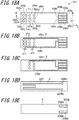
- FIGS. 1A to 1E are drawings showing a structural example of a multilayer-structured sensor board according to a first embodiment in the present disclosure.
- FIG. 1A is a top view of a sensor board 1;
- FIG. 1B is a view showing a wiring configuration in the second layer of the sensor board 1;
- FIG. 1C is a view showing a wiring configuration in the third layer of the sensor board 1;
- FIG. 1D is a view showing a heat-generating electrode configuration in the fourth layer of the sensor board 1;
- FIG. 1E is a bottom view of the sensor board 1.
- FIG. 2 is a sectional view taken along the line A-A of FIG. 1A .
- the sensor board 1 is used in a sensor device which detects PM (Particulate Matter) such as soot contained in exhaust gas from a diesel engine vehicle or a gasoline engine vehicle (for example, the sensor board is disposed in an exhaust passage for automotive exhaust gas).
- the sensor board 1 comprises: an insulating substrate 2; at least a pair of positive and negative columnar sensing electrodes 3a and 3b which are exposed at one surface (first face) of the insulating substrate 2; and innerlayer wiring lines 6a and 6b that are embedded within the insulating substrate 2 and correspond to the sensing electrodes 3a and 3b.
- the sensor board 1 achieves, as its feature, an improvement in the degree of sensitivity for detection of particulate matter, etc. by narrowing a gap between the sensing electrodes when adopted in a sensor device.
- the first layer, the second layer, or the third layer of the sensor board 1 is provided with electrode terminals 4a to 4d, internal wiring lines 5a to 5d, and innerlayer wiring lines 6a to 6d corresponding to sensing electrodes 3a to 3d.
- a heat-generating electrode 7 is embedded within the fourth layer of the sensor board 1, and, the fourth layer or the fifth layer is provided with internal wiring lines 8a and 8b and connection pads 9a and 9b corresponding to positive and negative electrodes of the heat-generating electrode 7.
- the sensing electrodes 3a to 3d are each a cylindrical electrode having an upper surface thereof exposed at a first face 2a of the insulating substrate 2. The upper surface and the first face 2a are flush with each other.
- the sensing electrode 3a is connected, via the internal wiring line 5a connected to the innerlayer wiring line 6a of the third layer and the electrode terminal 4a of the first layer, to a positive electrode of an external DC power supply (not shown) set for 50 [V], for example.
- the sensing electrode 3b is connected, via the internal wiring line 5b connected to the innerlayer wiring line 6b of the second layer and the electrode terminal 4b of the first layer, to a negative electrode of the external DC power supply.
- the sensing electrode 3c is connected, via the internal wiring line 5c, to the positive electrode of the DC power supply, and, like the sensing electrode 3b, the sensing electrode 3d is connected, via the internal wiring line 5d, to the positive electrode of the DC power supply.
- the sensing electrode 3a constitutes, in conjunction with the sensing electrode 3b or the sensing electrode 3d, a pair of positive and negative sensing electrodes
- the sensing electrode 3c constitutes, in conjunction with the sensing electrode 3b or the sensing electrode 3d, a pair of positive and negative sensing electrodes.
- the heat-generating electrode 7 is connected, via the connection pads 9a and 9b, to an external DC power supply (not shown) set for 20 [V], for example.
- the heat-generating electrode 7 is heated to, for example, 700 [°C] for decomposition and removal of PM (Particulate Matter) adherent to the first face 2a.
- the insulating substrate 2 in the form of, for example, a rectangular flat plate, serves as a base body in which paired sensing electrodes, as well as a pair of sensing electrodes and the heat-generating electrode, are disposed so as to be electrically insulated from each other.
- the insulating substrate 2 is formed of a ceramic sintered body such as sintered aluminum oxide, sintered aluminum nitride, sintered mullite, sintered glass ceramic, or zirconia ceramic (sintered zirconium oxide).
- a stack of a plurality of insulating layers formed of such a ceramic sintered body constitutes the insulating substrate 2.
- the insulating substrate 2 is constructed of a stack of a plurality of insulating layers formed of sintered aluminum oxide
- the insulating substrate 2 can be manufactured in the following manner.
- the insulating substrate 2 is produced by adding raw powdery materials such as silicon oxide (SiO 2 ), magnesium oxide (MgO), and manganese oxide (Mn 2 O 3 ) serving as sintering aids to aluminum oxide (Al 2 O 3 ) powder constituting inorganic particles, adding suitable binder, solvent, and plasticizer to the powder mixture, kneading the mixture into a slurry, shaping the slurry into a sheet by a heretofore known technique such as the doctor blade method or the calender roll method to obtain a ceramic green sheet, subjecting the ceramic green sheet to suitable punching operation, stacking a plurality of the ceramic green sheets together on an as needed basis, and firing the stack at a high temperature (about 1300°C to 1600°C).
- raw powdery materials such as silicon oxide (SiO 2 ), magnesium oxide (MgO), and manganese oxide (Mn 2 O 3 ) serving as sintering aids to aluminum oxide (Al 2 O 3 ) powder constituting inorganic
- the insulating substrate 2 may include a crystal phase containing alumina and manganese, and a glass phase containing manganese.
- the crystal phase may contain, in addition to alumina, various ceramics such as mullite, zirconia, aluminum nitride, and glass ceramic.
- the glass phase is an amorphous phase which contains at least Mn 2 O 3 , and may further contain one or more oxides selected from among Si, Mg, Ca, Sr, B, Nb, Cr, and Co.
- the glass phase may alternatively be an amorphous phase containing Mn 2 O 3 , SiO 2 , and MgO.
- the manganese-containing glass phase exhibits good wettability to an alumina crystal phase.
- the glass phase permeates the surface layer of the insulating substrate 2 so as to cover the surfaces of crystal particles, and consequently most part of the glass phase remains in the surface layer.
- the sensing electrodes 3a to 3d are each made as a via (cylindrical) electrode.
- each sensing electrode is 50 ⁇ m in diameter, and, the distance between adjacent sensing electrodes is set at 10 ⁇ m.
- the diameter of each of the sensing electrodes 3a to 3d may be adjusted within the range of 20 ⁇ m to 100 ⁇ m, and the distance between adjacent sensing electrodes may be adjusted within the range of 5 ⁇ m to 50 ⁇ m.
- the insulating substrate 2 including such sensing electrodes 3a to 3d can be produced by using a method similar to a conventional via electrode-equipped circuit board manufacturing method.
- the sensing electrodes 3a to 3d serve to detect particulate matter such as soot in an environment where the sensor board is installed in the sensor device.
- particulate matter such as soot
- the electrical resistance between the pair of sensing electrodes varies, causing a change in leakage current flowing between the electrodes.
- the detection of the change in leakage current enables acquisition of information about particulate matter existing between the paired sensing electrodes.
- the sensing electrodes 3a to 3d contain a metal material which allows detection of the change in leakage current.
- Oxidation-resistant platinum may be used as the metal material contained in the sensing electrodes 3a to 3d.
- the metal material used for the sensing electrodes 3a to 3d may be a metal material which is highly resistant to oxidation in a high-temperature environment, for example, platinum, or a metal material capable of forming an oxide-containing passive film at a surface thereof.
- the metal material capable of forming an oxide-containing passive film at the surface thereof include a Fe-Ni-Cr-Ti-Al alloy and MoSi 2 metal.
- a thickness of the passive film is set to about 0.1 to 5 ⁇ m.
- the passive film having this level of thickness covers the surface region of the sensing electrodes 3a to 3d, and consequently the likelihood of oxidation of the whole or the most part of the sensing electrodes can be diminished.
- About 90% of the surface region of the sensing electrodes 3a to 3d in terms of area may be composed of a passive film.
- 90% or above of the area of the exposed surface region of the sensing electrodes 3a to 3d may be covered with a passive film. This reduces the likelihood that the whole of the sensing electrodes 3a to 3d will undergo oxidation.
- the surface region of the sensing electrodes 3a to 3d may be entirely composed of a passive film.
- the entire area of the exposed surface region of the sensing electrodes 3a to 3d may be covered with a passive film. This minimizes the likelihood that the whole of the sensing electrodes 3a to 3d will undergo oxidation.
- the exposed surfaces of the sensing electrodes 3a to 3d may be deposited with a metallic plating layer by electroplating or electroless plating.
- the metallic plating layer is formed of a metal which is highly resistant to corrosion and securely connectable with a connecting member, for example, nickel, copper, gold, or silver.
- the exposed surface is deposited successively with an about 0.5 to 10 ⁇ m-thick nickel plating layer and an about 0.1 to 3 ⁇ m-thick gold plating layer, or, an about 1 to 10 ⁇ m-thick nickel plating layer and an about 0.1 to 1 ⁇ m-thick silver plating layer. This makes it possible to suppress corrosion of the sensing electrodes 3a to 3d.
- a metallic plating layer formed of other metal than the aforementioned, for example, a palladium plating layer may be interposed.
- the surfaces of the sensing electrodes 3a to 3d and the electrode terminals 4a to 4d may be deposited with a metallic plating layer by electroplating or electroless plating.
- the metallic plating layer is formed of a metal which is highly resistant to corrosion and securely connectable with a connecting member, for example, nickel, copper, gold, or silver.
- the surface is deposited successively with an about 0.5 to 10 ⁇ m-thick nickel plating layer and an about 0.1 to 3 ⁇ m-thick gold plating layer, or, an about 1 to 10 ⁇ m-thick nickel plating layer and an about 0.1 to 1 ⁇ m-thick silver plating layer.
- the internal wiring lines 8a and 8b are formed within the insulating substrate 2 so as to be electrically connected to the connection pads 9a and 9b, respectively, disposed on the lower surface of the insulating substrate 2.
- the innerlayer wiring lines 6a to 6d are embedded within the insulating substrate 2 so as to lie between the first face 2a provided with the sensing electrodes 3a to 3d and the other opposite face (lower surface in the case shown in FIG. 1 ). This enables the sensing electrodes 3a to 3d to have external electrical connection via the innerlayer wiring lines 6a to 6d disposed within the insulating substrate 2.
- the connection of the innerlayer wiring lines 6a to 6d to the electrode terminals 4a to 4d of the first layer is made via different layers.
- the innerlayer wiring lines 6a to 6d may include a circuit-patterned wiring conductor (not marked with reference symbol) which is provided between the layers constituting the insulating substrate 2.
- the heat-generating electrode 7 is formed of, for example, a metal material similar to the metal material used for the sensing electrodes 3a to 3d, and in the interest of efficient heat generation in particular, examples thereof include a material containing iron, titanium, chromium, silicon, etc. having high electrical resistance. Moreover, the heat-generating electrode 7 may contain an oxidation-resistant metal, such as platinum or a Fe-Ni-Cr alloy, as a major constituent.
- the metal material used for the heat-generating electrode 7 is contained in an amount of, for example, about 80% by mass or above in the heat-generating electrode 7 as a major constituent of the heat-generating electrode 7.
- an inorganic component such as glass or ceramic may be added to the heat-generating electrode 7. Such an inorganic component serves for shrinkage control in a firing step of the heat-generating electrode 7-forming process, which is effected concurrently with a firing step of the insulating substrate 2-forming process,
- the sensing electrodes 3a to 3d In forming the sensing electrodes 3a to 3d, the electrode terminals 4a to 4d, the internal wiring lines 5a to 5d, the innerlayer wiring lines 6a to 6d, and the heat-generating electrode 7, for example, powder of the aforenamed metal materials with an organic solvent and a binder added is kneaded to prepare a metallic paste, and, the metallic paste is applied, in a predetermined pattern, to the surface of the ceramic green sheet for forming the insulating substrate 2, as well as embedded, in a predetermined pattern, in a through hole of the ceramic green sheet.
- the application or embedding of the metallic paste is effected by a printing technique such for example as the screen printing method.
- a plurality of the ceramic green sheets are stacked together so as to cover the printed patterns that define the sensing electrodes 3a to 3d, the electrode terminals 4a to 4d, the internal wiring lines 5a to 5d, the innerlayer wiring lines 6a to 6d, and the heat-generating electrode 7, with subsequent concurrent firing of the metallic pastes and the ceramic green sheets.
- FIG. 3 is a block diagram showing the functional structure of the sensor device incorporating the sensor board according to the first embodiment.
- the sensor device 10 according to this embodiment comprises the sensor board 1, an overall control section 20, and first to sixth soot detecting sections 31 to 36.
- a heater control section 40, a temperature detecting section 50, and a display section 60 may be provided in the sensor device 10.
- the overall control section 20 is, for example, a microcomputer which exercises overall control of the sensor device 10. More specifically, the overall control section 20 controls the first to sixth soot detecting sections 31 to 36 and the heater control section 40 on the basis of specified programs. Moreover, the overall control section 20 determines the condition of particulate matter distribution and the size of particulate matter on the basis of current values measured by the first to sixth soot detecting sections 31 to 36.
- the first soot detecting section 31 applies a predetermined voltage (for example, 50 [V]) supplied from an external DC power supply (not shown) to between the sensing electrodes 3a and 3b to detect particulate matter between these sensing electrodes. More specifically, the first soot detecting section 31 measures the value of electric current flowing between the sensing electrodes 3a and 3b.
- a predetermined voltage for example, 50 [V]
- an external DC power supply not shown
- the second soot detecting section 32 measures the value of electric current flowing between the sensing electrodes 3b and 3c to detect particulate matter between the sensing electrodes 3b and 3c.
- the third soot detecting section 33, the fourth soot detecting section 34, the fifth soot detecting section 35, and the sixth soot detecting section 36 perform current value measurement to detect particulate matter between the sensing electrodes 3c and 3d, between the sensing electrodes 3d and 3a, between the sensing electrodes 3a and 3c, and between the sensing electrodes 3b and 3d, respectively.
- the sensing electrodes corresponding to the fifth soot detecting section 35, as well as the sensing electrodes corresponding to the sixth soot detecting section 36, are identical in polarity. Thus, neither of the fifth soot detecting section 35 and the sixth soot detecting section 36 performs the above-described current value measurement.
- the heater control section 40 comprises, for example, a DC power supply set for 20 [V] to effect control of the heat-generating electrode 7 in a manner so as to heat to a predetermined temperature on a command from the overall control section 20.
- the temperature detecting section 50 comprises a temperature sensor to measure the temperature of the heat-generating electrode 7 on a command from the heater control section 40.
- the display section 60 is built as, for example, a liquid crystal display that shows the current values detected by the first to sixth soot detecting sections 31 to 36 on a command from the overall control section 20, the condition of particulate matter distribution, and the size of particulate matter, etc.
- the following describes a method for determining the condition of distribution of particulate matter adherent to the sensing electrodes 3a to 3d and the size of the particulate matter.
- FIGS. 4A to 4C are schematic diagrams for explaining how leakage current varies according to the size of soot adherent to the sensor board.
- FIG. 4A is a schematic diagram for explaining leakage current variation under adhesion of minute soot to the sensor board.
- FIG. 4B is a schematic diagram for explaining leakage current variation under adhesion of medium-sized soot to the sensor board.
- FIG. 4C is a schematic diagram for explaining leakage current variation under adhesion of large-sized soot to the sensor board.
- FIG. 4A there is shown a case where minute soot 51 has adhered to the sensor board.
- a leakage current flowing between electrodes A and B and a leakage current flowing between electrodes B and C have increased substantially equally (as indicated by Curve L1 and Curve L2).
- Curve L3 and Curve L4 When the leakage current between the electrodes A and B and the leakage current between the electrodes B and C increase at different increasing rates (as indicated by Curve L3 and Curve L4), then it is determined that the soot distribution between the electrodes A and B and the soot distribution between the electrodes B and C differ from each other (lack of uniformity in soot distribution).
- FIG. 4B there is shown a case where medium-sized soot 52 has adhered to the sensor board.
- the leakage current between the electrodes A and B has increased sharply (as indicated by Curve L5).
- it is determined that medium-sized soot has adhered to the sensor board in the electrode A-to-electrode B range at the point of time T2.
- FIG. 4C there is shown a case where large-sized soot 53 has adhered to the sensor board.
- both the leakage current between the electrodes A and B and the leakage current between the electrodes B and C have increased sharply.
- it is determined that large-sized soot has adhered to the sensor board both in the electrode A-to-electrode B range and in the electrode B-to-electrode C range at the point of time T3.
- FIG. 5 is a flowchart showing an algorithm for determination of the distribution and size of detection targets in the sensor device according to the first embodiment.
- the first to sixth soot detecting sections 31 to 36 perform current value measurement on a regular basis on a command from the overall control section 20 (S100), and, after a lapse of a predetermined period of time ("YES" at S102), the overall control section 20 effects a comparison of final current values on different electrode-to-electrode regions (S104).
- the overall control section 20 calculates the rate of current increase in each electrode-to-electrode region (S112). When the calculated value is less than or equal to a predetermined value ("YES" at S114), then the overall control section 20 judges that soot particle is minute (S116).
- FIGS. 6A to 6D are drawings showing a structural example of a multilayer-structured sensor board according to a second embodiment in the present disclosure.
- FIG. 6A is a top view of a sensor board 11;
- FIG. 6B is a view showing a wiring configuration in the second layer of the sensor board 11;
- FIG. 6C is a view showing a wiring configuration in the third layer of the sensor board 11;
- FIG. 6D is a bottom view of the sensor board 11.
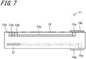
- FIG. 7 is a sectional view taken along the line B-B of FIG. 6A .
- the sensor board 11 achieves, as its feature, constructional simplicity and cost reduction while narrowing a gap between sensing electrodes when adopted in a sensor device.
- electrode terminals 14a and 14c, internal wiring lines 15a and 15c, and innerlayer wiring lines 16a and 16c are disposed at or embedded within the first layer or the second layer of the sensor board 11 corresponding to sensing electrodes 13a and 13b and sensing electrodes 13c and 13d.
- a heat-generating electrode 17 is embedded within the third layer of the sensor board 11, and, internal wiring lines 18a and 18b and connection pads 19a and 19b are disposed at or embedded within the third layer or the fourth layer corresponding to the positive and negative sides of the heat-generating electrode 17.
- the sensing electrodes 13a to 13d are each a cylindrical electrode having an upper surface thereof exposed at a first face 12a of an insulating substrate 12, and, each upper surface is flush with the first face 12a.
- the sensing electrodes 13a and 13b are connected to a positive electrode of an external DC power supply (not shown) set for 50 [V] for example, whereas the sensing electrodes 13c and 13d are connected to a negative electrode of the DC power supply.
- the sensing electrode 13a constitutes, in conjunction with the sensing electrode 13d, a pair of positive and negative sensing electrodes
- the sensing electrode 13b constitutes, in conjunction with the sensing electrode 13c, a pair of positive and negative sensing electrodes.
- a plurality of pairs of sensing electrodes have a common positive-negative electrode arrangement.
- FIGS. 8A to 8C are drawings each showing modified examples of the sensing electrodes 3a to 3d or sensing electrodes 13a to 13d in respect of electrode configuration and electrode arrangement.
- FIG. 8A is a view showing a modified example obtained by combining circular sensing electrodes having different diameters.
- a sensing electrode 51e and each of sensing electrodes 51a to 51d while being identically circular-shaped as seen from above, differ in diameter from each other (L11 is set at 50 ⁇ m, whereas L12 is set at 25 ⁇ m).
- the distance between the electrodes is set at 10 ⁇ m.
- FIG. 8A for example, where voltage application is effected in a manner such that the sensing electrode 51e becomes a positive electrode, and each of the sensing electrodes 51a to 51d becomes a negative electrode, four pairs of sensing electrodes are formed.
- FIG. 8B is a view showing a modified example obtained by changing the circular profile of each sensing electrode shown in FIG. 8A to an octagonal profile.
- electrode diameter and electrode distance for example, L21 is set at 50 ⁇ m, a21 is set at 10 ⁇ m, and b21 is set at 10 ⁇ m.
- FIG. 8C is a view showing a modified example obtained by changing the circular profile of the sensing electrode according to the first embodiment to a square profile.
- electrode size and electrode distance for example, L31 is set at 50 ⁇ m, a31 is set at 10 ⁇ m, and b31 is set at 10 ⁇ m.
- the profile of the sensing electrode of the above-described embodiment is not limited to this, but may be an elliptical profile or other polygonal profile.
- the functions of the first to sixth soot detecting sections 31 to 36 of the first embodiment may be integrated into a single first soot detecting section. In this case, detection of particulate matter (for example, measurement of leakage current, etc.) between the sensing electrodes is effected by operating switches provided in the first soot detecting section in a manner permitting sequential connection changeover.
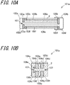
- FIGS. 9A to 9G and FIGS. 10A and 10B are drawings showing a structural example of a sensor board according to a third embodiment.
- FIG. 9A is a top view of a sensor board 101a according to this embodiment;
- FIGS. 9B and 9C are views showing wiring configurations in the second and third layers, respectively, of the sensor board 101a;
- FIG. 9D is a view showing a heat-generating electrode configuration in the fourth layer of the sensor board 101a;
- FIGS. 9E and 9F are views showing wiring configurations in the fifth and sixth layers, respectively, of the sensor board 101a;
- FIG. 9G is a bottom view of the sensor board 101a.
- FIG. 10A is a sectional view taken along the line C-C of FIG. 9A
- FIG. 10B is a sectional view taken along the line D-D of FIG. 9A .
- the sensor board 101a is also used in a sensor device designed for PM detection.
- sensing electrodes which are made at least as a pair of positive and negative electrodes, located at each of one surface of an insulating substrate in the form of a rectangular prism (for example, a top face corresponding to the first face of the sensor board according to the first embodiment) and other surface than the one surface thereof (for example, a back face).
- Part of each of the positive and negative electrodes constituting the pair of sensing electrodes is exposed at the one surface or the other surface of the insulating substrate. In the case shown in FIGS.
- sensing electrodes 103a to 103h each in the form of a column, constituting pairs of the positive and negative sensing electrodes, and innerlayer wiring lines 106a to 106h embedded within the insulating substrate 2 corresponding to the sensing electrodes 103a to 103h.
- the pairs of positive and negative sensing electrodes are electrodes in column form (hereafter also referred to as "columnar electrodes"), or comb-like electrodes in an interdigitated array form.
- the sensing electrodes may be constructed of a columnar electrode and interdigitated comb-like electrodes disposed in mutually corresponding relation.
- the sensing electrodes 103a to 103d there are provided the sensing electrodes 103a to 103d, and, electrode terminals 104a to 104d, internal wiring lines 105a to 105c, and the innerlayer wiring lines 106a to 106d corresponding to the sensing electrodes 103a to 103d.
- the fourth layer of the sensor board 101a has a heat-generating electrode 107 embedded therein, and also has the internal wiring lines 105b and 108a corresponding to the heat-generating electrode 107.
- a region including the sensing electrodes 103a to 103d for detection of particulate matter is defined as a sensing region 109.
- the heat-generating electrode 107 is embedded along the outer periphery of the sensing region 109 as seen in plan perspective view.
- the sensing electrodes 103e to 103h there are provided the sensing electrodes 103e to 103h, and, electrode terminals 104e to 104g, internal wiring lines 105e to 105g, and the innerlayer wiring lines 106e to 106h corresponding to the sensing electrodes 103e to 103h.
- the sensing electrodes 103a to 103d, as well as the sensing electrodes 103e to 103h, are connected, via the electrode terminals 104a to 104d, as well as the electrode terminals 104e to 104g, to a positive or negative electrode of an external DC power supply (not shown).
- the heat-generating electrode 107 is connected, via the electrode terminals 104b and 104d, to the external DC power supply.
- the electrode terminal 104b is connected to both of the negative electrode in the group of the sensing electrodes 103a to 103d and the negative side of the heat-generating electrode 107 as a common negative terminal, an extra terminal specific to the negative side of the heat-generating electrode 107 may be provided without shared use of the electrode terminal 104b.
- the electrode terminals 104a to 104g may be further provided with a connecting member such as a connection pad, not shown, to establish connection with an external power supply, a sensing circuit for measurement, etc. The following describes specifics of the individual constituent components of this embodiment.
- the sensing electrodes 103a to 103h are each a cylindrical electrode, part of which is exposed at one surface (first face) 2a or the other surface (second face) 2b of the insulating substrate 2. In this case, it is advisable that the upper surface of each of the sensing electrodes 103a to 103d is flush with the one surface 2a, and the upper surface of each of the sensing electrodes 103e to 103h is flush with the other surface 2b.
- the sensing electrode 103a, 103c is connected, via the internal wiring line 105a, 105c connected to the innerlayer wiring line 106a, 106c and the electrode terminal 104a, 104c, to a positive electrode of an external DC power supply set for 50 [V], for example.
- the sensing electrode 103b, 103d is connected, via the internal wiring line 105b connected to the innerlayer wiring line 106b and the electrode terminal 104b, to a negative electrode of the DC power supply.
- the sensing electrode 103e, 103g is connected, via the internal wiring line 105e, 105g connected to the innerlayer wiring line 106e, 106g and the electrode terminal 104e, 104g, to the positive electrode of the DC power supply.
- the sensing electrode 103f, 103h is connected, via the internal wiring line 105f connected to the innerlayer wiring line 106f and the electrode terminal 104f, to the negative electrode of the DC power supply.
- the sensing electrode 103a constitutes, in conjunction with the sensing electrode 103b or the sensing electrode 103d, a pair of positive and negative sensing electrodes
- the sensing electrode 103c constitutes, in conjunction with the sensing electrode 103b or the sensing electrode 103d, a pair of positive and negative sensing electrodes
- the sensing electrode 103e constitutes, in conjunction with the sensing electrode 103f or the sensing electrode 103h, a pair of positive and negative sensing electrodes
- the sensing electrode 103g constitutes, in conjunction with the sensing electrode 103f or the sensing electrode 103h, a pair of positive and negative sensing electrodes.
- the heat-generating electrode 107 is heated to, for example, 700 [°C] for decomposition and removal of particulate matter adherent to the vicinity of the sensing electrodes 103a to 103d, as well as the vicinity of the sensing electrodes 103e to 103h.
- the insulating substrate 2 in the form of, for example, a rectangular prism, serves as a base body in which the pair of sensing electrodes, as well as the pair of sensing electrodes and the heat-generating electrode, are disposed so as to be electrically insulated from each other.
- the sensing electrodes 103a to 103h are each made as a via (cylindrical) electrode.
- each sensing electrode is 50 ⁇ m in diameter, and, the distance between adjacent sensing electrodes is set at 10 ⁇ m.
- the diameter of each of the sensing electrodes 103a to 103h may be adjusted within the range of 20 ⁇ m to 100 ⁇ m, and the distance between adjacent sensing electrodes may be adjusted within the range of 5 ⁇ m to 50 ⁇ m.
- the insulating substrate 2 including such sensing electrodes 103a to 103h can be produced by using a method similar to a conventional via electrode-equipped circuit board manufacturing method.
- the sensing electrodes 103a to 103h serve to detect particulate matter in an environment where the sensor board is installed in the sensor device.
- particulate matter such as soot
- the electrical resistance between the pair of sensing electrodes varies, causing a change in leakage current flowing between the electrodes.
- the detection of the change in leakage current enables acquisition of information about particulate matter existing between the pair of sensing electrodes.
- the sensing electrodes 103a to 103h contain a metal material that allows detection of the change in leakage current.
- Oxidation-resistant platinum may be used as the metal material contained in the sensing electrodes 103a to 103h.
- a metal material similar to the metal material used for the earlier described sensing electrodes 3a to 3d may be used for the sensing electrodes 103a to 103h.
- a metallic plating layer similar to the metallic plating layer formed on the sensing electrodes 3a to 3d may be deposited on the surfaces of the sensing electrodes 103a to 103h, the electrode terminals 104a to 104g, etc. by electroplating or electroless plating.
- Each of the innerlayer wiring lines 106a to 106d is formed in the second or third layer of the insulating substrate 2 to provide electrical connection between the sensing electrodes 103a to 103d and the electrode terminals 104a to 104d in the first layer.
- each of the innerlayer wiring lines 106e to 106h is formed in the sixth or fifth layer of the insulating substrate 2 to provide electrical connection between the sensing electrodes 103e to 103h and the electrode terminals 104e to 104g in the seventh layer.
- the heat-generating electrode 107 is formed of a metal material similar to the metal material used for the heat-generating electrode 7, and may further contain an inorganic component.
- the sensing electrodes 103a to 103h can be formed by the same production method as that of the sensing electrodes 3a to 3d of the first embodiment.
- the electrode terminals 104a to 104g can be formed by the same production method as that of the electrode terminals 4a to 4d
- the internal wiring lines 105a to 105g can be formed by the same production method as that of the internal wiring lines 5a to 5d
- the innerlayer wiring lines 106a to 106h can be formed by the same production method as that of the innerlayer wiring lines 6a to 6d
- the heat-generating electrode 107 can be formed by the same production method as that of the heat-generating electrode 7.
- the sensor board 101a achieves an improvement in the degree of sensitivity for detection of particulate matter without the necessity of sensor resizing, and is also capable of long-duration continuous measurement. Moreover, the sensor board 101a achieves further improvement in the degree of sensitivity for detection by using very closely spaced-apart columnar sensing electrodes.
- FIG. 11 is a sectional view showing a structural example of a sensor device utilizing the sensor board according to the present embodiment.
- a sensor device 100 comprises the sensor board 101a, necessary power supplies 120 and 130, and a measurement detection circuit 140. Note that constituent components common to the construction shown in FIG. 11 and the construction shown in FIGS. 9A to 9G , etc. will be identified with the same reference symbol, and overlapping descriptions will be omitted.
- the measurement detection circuit 140 detects leakage current on the basis of particulate matter accumulated between the positive and negative electrodes, and calculates the resistance between the positive and negative electrodes, etc.
- the power supply 120, 130 and the measurement detection circuit 140 can be implemented by the application of the power supply and the measurement detection circuit (that is, the overall control section 20, the first to sixth soot detecting sections 31 to 36, the heater control section 40, the temperature detecting section 50, the display section 60, etc.) of the first embodiment.
- the measurement detection circuit 140 effects detection of leakage current, etc. for each pair of sensing electrodes on a time-division basis.
- a conductor for connection such as a conductive connecting member, used to provide electrical connection between a lead terminal 110a, 110b and the power supply 120, 130 is schematically shown by a phantom line (chain double-dashed line).
- the lead terminals 110a and 110b are not directly conducive to particulate matter detection.
- materials used to form the lead terminals 110a and 110b are suitably selected with consideration given to an environment where the sensor device is operated, the productivity of the sensor board 101a, cost effectiveness, and other conditions.
- the use of the lead terminals 110a and 110b formed of a highly oxidation-resistant metal material such as platinum or gold brings about an advantage in reliability to the sensor device 100.
- the lead terminals 110a and 110b may be formed of an iron-based alloy such as an iron-nickel-cobalt alloy, or may be constructed of a copper-made member, for example. Where the lead terminals 110a and 110b are formed of the iron-based alloy, their exposed surfaces may be formed with a plating layer such as a gold plating layer for protection.
- the lead terminal 110a, 110b is joined to the electrode terminal 104a, etc. by a brazing material (not marked with reference symbol) such as silver solder (silver-copper solder) or gold solder.
- a brazing material for use is suitably selected with consideration given to various conditions set for the manufacture or usage of the sensor board 101a.
- the sensing electrodes are formed from a 2 by 2 matrix of columnar electrodes (four electrodes in total) in the present embodiment, the number of the sensing electrodes is not limited to this.
- the sensing electrodes may be formed from an n by m matrix of electrodes (wherein n is greater than or equal to 2, and m is less than or equal to 200).
- sensing electrode is disposed at the back face opposed to the one surface as the other surface, for example, in addition to the back face, two side faces contiguous to the one surface may be provided with the sensing electrode.
- the columnar sensing electrode of the above-described embodiment is not limited to the cylindrical electrode, but may be given the form of an elliptical column or other polygonal column.
- FIGS. 12A to 12E are drawings showing a structural example of a sensor board according to a fourth embodiment.
- FIG. 12A is a top view of a sensor board 101b according to this embodiment
- FIGS. 12B and 12D are views showing an example of wiring configurations in the second and fourth layers, respectively, of the sensor board 101b
- FIG. 12C is a view showing an example of a heat-generating electrode configuration in the third layer of the sensor board 101b
- FIG. 12E is a bottom view of the sensor board 101b.
- FIG. 13A is a sectional view taken along the line E-E of FIG. 12A
- FIG. 13B is a sectional view taken along the line F-F of FIG. 12A .
- sensing electrodes 113a to 113i there are provided sensing electrodes 113a to 113i, and, electrode terminals 114a to 114c, internal wiring lines 115a, 115b, and 118a, and innerlayer wiring lines 116a to 116c corresponding to the sensing electrodes 113a to 113i.
- the third layer of the sensor board 101b has a heat-generating electrode 117 embedded therein, and also has the internal wiring lines 115b and 118a corresponding to the heat-generating electrode 117.
- sensing electrodes 113j to 113r there are provided sensing electrodes 113j to 113r, and, electrode terminals 114j and 114k, internal wiring lines 115j and 115k, and innerlayer wiring lines 116j to 1161 corresponding to the sensing electrodes 113j to 113r.
- the sensing electrodes 113a to 113i and the sensing electrodes 113j to 113r are each a cylindrical electrode having an upper surface thereof exposed at one surface 2a or the other surface 2b of an insulating substrate 2, and, each upper surface is flush with the one or other surface.
- the sensing electrodes 113d to 113f and the sensing electrodes 113m to 113o are connected to a positive electrode of an external DC power supply (not shown) set for 50 [V] for example, whereas the sensing electrodes 113a to 113c, those 113g to 113i, those 113j to 1131, and those 113p to 113r are connected to a negative electrode of the DC power supply.
- the sensing electrodes 113d to 113f constitute, in conjunction with the sensing electrodes 113a to 113c or the sensing electrodes 113g to 113i, a pair of positive and negative sensing electrodes
- the sensing electrodes 113m to 113o constitute, in conjunction with the sensing electrodes 113j to 1131 or the sensing electrodes 113p to 113r, a pair of positive and negative sensing electrodes.
- the sensing electrodes 113a to 113i and the sensing electrodes 113j to 113r are designed so that those aligned in a horizontal row are interchangeable.
- the sensor board 101b achieves an improvement in the degree of sensitivity for detection of particulate matter without the necessity of sensor resizing, and is also capable of long-duration continuous measurement. Moreover, the sensor board 101b has a larger number of columnar sensing electrodes, yet can achieve simplification in the configuration of the innerlayer wiring line provided within the insulating substrate with no increase in cost.
- a sensor device according to this embodiment (not shown) can be implemented by the application of the sensor device 100 according to the third embodiment. Thus, the description of operation of the sensor device will be omitted.
- FIGS. 14A to 14D are drawings showing a structural example of a sensor board according to a fifth embodiment.
- FIG. 14A is a top view of a sensor board 101c according to this embodiment;
- FIGS. 14B and 14C are views showing an example of heat-generating electrode configurations in the second and third layers, respectively, of the sensor board 101c;
- FIG. 14D is a bottom view of the sensor board 101c.
- FIG. 15A is a sectional view taken along the line G-G of FIG. 14A
- FIG. 15B is a sectional view taken along the line H-H of FIG. 14A .
- the sensor board 101c according to this embodiment comprising interdigitated comb-like electrodes serving as sensing electrodes can be produced by a conventional manufacturing method. Moreover, constituent components common to the embodiment shown in FIGS. 14A to 14D , 15A, and 15B and the preceding embodiment shown in FIGS. 9A to 9G , 10A, and 10B will be identified with the same reference symbol, and overlapping descriptions will be omitted.
- the first and fourth layers of the sensor board 101c are provided with sensing electrodes 123a and 123b and sensing electrodes 123c and 123d, respectively, and, the second and third layers of the sensor board 101c are provided with heat-generating electrodes 127a and 127b, respectively.
- a region including the sensing electrodes 123a and 123b or the sensing electrodes 123c and 123d is defined as a sensing region 129.
- the heat-generating electrode 127a or 127b is embedded along the outer periphery of the sensing region 129 as seen in plan perspective view.
- the sensing electrodes 123a to 123d in interdigitated array form are exposed at one surface 2a or the other surface 2b of an insulating substrate.
- the sensing electrode 123a constitutes, in conjunction with the sensing electrode 123b, a pair of positive and negative sensing electrodes
- the sensing electrode 123c constitutes, in conjunction with the sensing electrode 123d, a pair of positive and negative sensing electrodes.
- the sensing electrodes 123a and 123c are connected to a positive electrode of an external DC power supply (not shown) set for 50 [V], for example, and, the sensing electrodes 123b and 123d are connected to a negative electrode of the DC power supply.
- the sensor board 101c can achieve an improvement in the degree of sensitivity for detection of particulate matter without the necessity of sensor resizing, and is also capable of long-duration continuous measurement.
- an interdigitated array of comb-like electrodes in the first layer and an interdigitated array of comb-like electrodes in the fourth layer are disposed in symmetrical relation. This arrangement can suppress deformation caused by thermal stress during a firing process.
- a sensor device according to this embodiment (not shown) can be implemented by the application of the sensor device 100 according to the third embodiment, and the description of operation of the sensor device will thus be omitted.
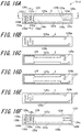
- FIGS. 16A to 16F are drawings showing a structural example of a sensor board according to a sixth embodiment.
- a sensor board 101d according to this embodiment is constructed by providing additional electrodes in column form (hereafter referred to as "columnar electrodes") 133a to 133e and 134a to 134d and columnar electrodes 135a to 135d and 136a to 134e in the sensor board 101c according to the fifth embodiment.
- the columnar electrodes 133a to 133e and the columnar electrodes 134a to 134d are connected to corresponding one of the interdigitated comb-like electrodes 123a and 123b above, and the columnar electrodes 135a to 135d and the columnar electrodes 136a to 134e are connected to corresponding one of the interdigitated comb-like electrodes 123c and 123d below.
- FIG. 16A is a top view of the sensor board 101d according to this embodiment
- FIG. 16B is a view showing an example of a wiring configuration in the second layer of the sensor board 101d according to this embodiment
- FIGS. 16C and 16D are views showing an example of heat-generating electrode configurations in the third and fourth layers, respectively, of the sensor board 101d
- FIG. 16E is a view showing an example of a wiring configuration in the fifth layer of the sensor board 101d
- FIG. 16F is a bottom view of the sensor board 101d.
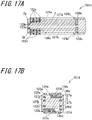
- FIG. 17A is a sectional view taken along the line I-I of FIG. 16A
- FIG. 17B is a sectional view taken along the line J-J of FIG. 16A .
- the sensor board 101d comprising the interdigitated comb-like electrodes 123a to 123d and the columnar electrodes 133a to 133e, 134a to 134d, 135a to 135d, and 136a to 136e can be produced by a conventional manufacturing method. Moreover, constituent components common to the embodiment shown in FIGS. 16A to 16F , 17A, and 17B and the preceding embodiment shown in FIGS. 14A to 14D , 15A, and 15B will be identified with the same reference symbol, and overlapping descriptions will be omitted.
- the second layer of the sensor board 101d has the columnar electrodes 133a to 133e corresponding to the comb-like electrode 123a and the columnar electrodes 134a to 134d corresponding to the comb-like electrode 123b.
- the fifth layer of the sensor board 101d has the columnar electrodes 135a to 135d corresponding to the comb-like electrode 123c, and the columnar electrodes 136a to 136e corresponding to the comb-like electrode 123d.
- the comb-like electrode 123a is securely held by the columnar electrodes 133a to 133e
- the comb-like electrode 123b is securely held by the columnar electrodes 134a to 134d
- the comb-like electrode 123c is securely held by the columnar electrodes 135a to 134d
- the comb-like electrode 123d is securely held by the columnar electrodes 136a to 136e.
- This arrangement can prevent separation of the interdigitated comb-like electrodes 123a to 123d.
- a sensor device according to this embodiment (not shown) can be implemented by the application of the sensor device 100 according to the third embodiment, and the description of operation of the sensor device will thus be omitted.
- FIGS. 18A to 18E and FIGS. 19A and 19B are drawings showing a structural example of a sensor board according to a seventh embodiment.
- FIG. 18A is a top view of a sensor board 201 according to this embodiment;
- FIGS. 18B and 18C are views showing wiring configurations in the second and third layers, respectively, of the sensor board 201;
- FIG. 18D is a view showing a heat-generating electrode configuration in the fourth layer of the sensor board 201;
- FIG. 18E is a bottom view of the sensor board 201.
- FIG. 19A is a sectional view taken along the line K-K of FIG. 18A
- FIG. 19B is a sectional view taken along the line L-L of FIG. 18A .
- the sensor board 201 is also used in a sensor device designed for PM detection.
- the sensor board 201 is constructed of an insulating substrate shaped in a flat plate, the surface of which is provided with a first positive sensing electrode and a first negative sensing electrode adjacent to the first positive sensing electrode, and a second positive sensing electrode and a second negative sensing electrode adjacent to the second positive sensing electrode, constituting pairs of positive and negative electrodes.
- the sensor board 201 is characterized in that, at least in one direction (for example, in a direction x shown in FIG.
- a distance between the first positive sensing electrode and the first negative sensing electrode, which is defined as a first electrode distance, and a distance between the second positive sensing electrode and the second negative sensing electrode, which is defined as a second electrode distance, differ from each other.
- the pairs of positive and negative sensing electrodes are not limited to the columnar electrodes, but may be of interdigitated comb-like electrodes.
- the sensing electrodes may be constructed of a columnar electrode and interdigitated comb-like electrodes disposed in mutually corresponding relation.
- the sensing electrodes 203a to 2031 there are provided the sensing electrodes 203a to 2031, and, electrode terminals 204a to 204d, internal wiring lines 205a to 205d, and the innerlayer wiring lines 206a to 206d corresponding to the sensing electrodes 203a to 2031.
- the fourth layer of the sensor board 201 has a heat-generating electrode 207 embedded therein, and also has internal wiring lines 208a and 208b and connection pads 209a and 209b corresponding to the heat-generating electrode 207.
- the sensing electrodes 203a to 2031 are connected, via the corresponding electrode terminals 204a to 204d, to a positive or negative electrode of an external DC power supply (not shown). Moreover, the heat-generating electrode 207 is connected, via the connection pads 209a and 209b, to the external DC power supply.
- the sensing electrodes 203a to 2031 are each a cylindrical electrode, part of which is exposed at one surface 2a of the insulating substrate 2. In this case, the upper surface of each of the sensing electrodes 203a to 2031 may be flush with the one surface 2a.
- the sensing electrode 203a, 203e, 203i is connected, via the internal wiring line 205a connected to the innerlayer wiring line 206a and the electrode terminal 204a, to the positive electrode of the external DC power supply set for 50 [V], for example, and also the sensing electrode 203c, 203g, 203k is connected, via the internal wiring line 205c connected to the innerlayer wiring line 206c and the electrode terminal 204c, to the positive electrode of the external DC power supply.
- the sensing electrode 203b, 203f, 203j is connected, via the internal wiring line 205b connected to the innerlayer wiring line 206b and the electrode terminal 204b, to the negative electrode of the external DC power supply, and also the sensing electrode 203d, 203h, 2031 is connected, via the internal wiring line 205d connected to the innerlayer wiring line 206d and the electrode terminal 204d, to the negative electrode of the external DC power supply.
- each of groups of three aligned in a vertical row exhibits one and the same positive or negative polarity.
- the electrode group A consisting of the sensing electrodes 203a, 203e, and 203i constitutes, in conjunction with the electrode group B consisting of the sensing electrodes 203b, 203f, and 203j, a pair of positive and negative sensing electrodes
- the electrode group C consisting of the sensing electrodes 203c, 203g, and 203k constitutes, in conjunction with the electrode group D consisting of the sensing electrodes 203d, 203h, and 2031, a pair of positive and negative sensing electrodes.
- the electrode groups A to D are disposed with a gradual increase in electrode distance in the x direction, that is; they are disposed with various spacings. For example, as shown in FIG. 18B , given that a distance between the electrode group A and the electrode group B is "d11", then a distance between the electrode group B and the electrode group C defined as "d12" is equal to a value corresponding to "2d11", and a distance between the electrode group C and the electrode group B defined as "d13" is equal to a value corresponding to "4d11".
- vertically-aligned three sensing electrodes are made as interchangeable electrodes of the same positive or negative polarity in the case given above, horizontally-aligned three sensing electrodes may be made similarly as interchangeable electrodes instead.
- the heat-generating electrode 207 is heated to, for example, 700 [°C] for decomposition and removal of particulate matter adherent to the vicinity of the sensing electrodes 203a to 2031.
- the insulating substrate 2 in the form of, for example, a flat plate, serves as a base body in which a pair of sensing electrodes, as well as a pair of sensing electrodes and the heat-generating electrode 207, are disposed so as to be electrically insulated from each other.
- the sensing electrodes 203a to 2031 are each made as a columnar electrode (for example, a cylindrical electrode).
- each sensing electrode has a diameter of 20 ⁇ m to 100 ⁇ m, and, the distance between adjacent sensing electrodes is adjusted within the range of 5 ⁇ m to 50 ⁇ m.
- the insulating substrate 2 including such sensing electrodes 203a to 2031 can be produced by using a method similar to a conventional via (through conductor)-equipped circuit board manufacturing method.
- the sensing electrodes 203a to 2031 serve to detect particulate matter in an environment where the sensor board is installed in the sensor device.
- particulate matter such as soot
- the electrical resistance between the pair of sensing electrodes varies, causing a change in leakage current flowing between the electrodes.
- the detection of the change in leakage current enables acquisition of information about particulate matter existing between the paired sensing electrodes.
- the sensing electrodes 203a to 2031 contain a metal material which allows detection of the change in leakage current.
- Oxidation-resistant platinum may be used as the metal material contained in the sensing electrodes 203a to 2031.
- a metal material similar to the metal material used for the earlier described sensing electrodes 3a to 3d may be used for the sensing electrodes 203a to 2031.
- a metallic plating layer similar to the metallic plating layer formed on the sensing electrodes 3a to 3d may be deposited on the surfaces of the sensing electrodes 203a to 2031, the electrode terminals 204a to 204d, etc. by electroplating or electroless plating.
- Each of the innerlayer wiring lines 206a to 206d is formed in the second or third layer of the insulating substrate 2 to provide electrical connection between the sensing electrodes 203a to 2031 and the electrode terminals 204a to 204d in the first layer.
- the heat-generating electrode 207 is formed of a metal material similar to the metal material used for the heat-generating electrode 7.
- the sensing electrodes 203a to 2031 can be formed by the same production method as that of the sensing electrodes 3a to 3d of the first embodiment.
- the electrode terminals 204a to 204d can be formed by the same production method as that of the electrode terminals 4a to 4d
- the internal wiring lines 205a to 205d can be formed by the same production method as that of the internal wiring lines 5a to 5d
- the innerlayer wiring lines 206a to 206d can be formed by the same production method as that of the innerlayer wiring lines 6a to 6d
- the heat-generating electrode 207 can be formed by the same production method as that of the heat-generating electrode 7.
- the sensor board 201 is capable of long-duration continuous detection while allowing responsivity regardless of the concentration of particulate matter contained in exhaust gas.
- FIG. 20 is a sectional view showing a structural example of a sensor device utilizing the sensor board according to the present embodiment.
- a sensor device 200 comprises the sensor board 201, necessary power supplies 220 and 230, and a measurement detection circuit 240.
- constituent components common to the construction shown in FIG. 20 and the construction shown in FIGS. 18A to 18E , etc. will be identified with the same reference symbol, and overlapping descriptions will be omitted.
- the measurement detection circuit 240 detects leakage current on the basis of particulate matter accumulated between the positive and negative electrodes, and calculates the resistance between the positive and negative electrodes, etc.
- the power supply 220, 230 and the measurement detection circuit 240 can be implemented by the application of the power supply and the measurement detection circuit (that is, the overall control section 20, the first to sixth soot detecting sections 31 to 36, the heater control section 40, the temperature detecting section 50, the display section 60, etc.) of the first embodiment.
- the measurement detection circuit 240 effects detection of leakage current, etc. for each pair of sensing electrodes on a time-division basis.
- a conductor for connection such as a conductive connecting member, used to provide electrical connection between a lead terminal 210a, 210b and the power supply 220, 230 is schematically shown by a phantom line (chain double-dashed line).
- the lead terminals 210a and 210b are not directly conducive to particulate matter detection.
- materials used to form the lead terminals 210a and 210b are suitably selected with consideration given to an environment where the sensor device is operated, the productivity of the sensor board 201, cost effectiveness, and other conditions.
- the use of the lead terminals 210a and 210b formed of a highly oxidation-resistant metal material such as platinum or gold brings about an advantage in reliability to the sensor device 200.
- the lead terminals 210a and 210b may be formed of an iron-based alloy such as an iron-nickel-cobalt alloy, or may be constructed of a copper-made member, for example. Where the lead terminals 210a and 210b are formed of the iron-based alloy, their exposed surfaces may be protected by a plating layer such as a gold plating layer.
- the lead terminal 210a, 210b is joined to the electrode terminal 204a, etc. by a brazing material (not marked with reference symbol) such as silver solder (silver-copper solder) or gold solder.
- a brazing material for use is suitably selected with consideration given to various conditions set for the manufacture or usage of the sensor board 201.
- the sensing electrodes are formed from a 3 by 4 matrix of columnar electrodes (twelve electrodes in total) in the present embodiment, the number of the sensing electrodes is not limited to this.
- the sensing electrodes may be formed from an n by m matrix of electrodes (wherein n is greater than or equal to 2, and m is less than or equal to 200).
- the columnar sensing electrode of the above-described embodiment is not limited to the cylindrical electrode, but may be given the form of an elliptical column or other polygonal column.
- FIGS. 21A to 21C are each a top view of a sensor board implemented as an example according to an eighth embodiment, illustrating an arrangement of sensing electrodes.
- the following description of this embodiment deals with arrangements of other sensing electrodes than those provided in the sensor board according to the seventh embodiment (columnar sensing electrodes, in particular).
- constituent components common to the implementation examples shown in FIGS. 21A to 21C and the preceding embodiment shown in FIGS. 18A to 18E , 19A, and 19B will be identified with the same reference symbol, and overlapping descriptions will be omitted.
- FIG. 21A is a top view of the sensor board implemented as a first example according to this embodiment.
- the sensor board 202A is also used in a sensor device designed for detection of particulate matter contained in exhaust gas, and its detection performance is equivalent to that of the sensor board 201.
- x and y axes there are provided.
- the sensor board 202A like the sensor board 201, there are successively disposed, in left-to-right order, an electrode group A, an electrode group B, an electrode group C, and an electrode group D.
- the electrode group A and the electrode group C are connected to a positive electrode of a power supply (not shown) whereas the electrode group B and the electrode group D are connected to a negative electrode of the power supply.
- the sensor boards shown in FIGS. 21B and 21C are each provided with an arrangement of electrode groups.
- a distance between the electrode group A and the electrode group B is set at d13 (equal to a value corresponding to 4d11)
- a distance between the electrode group B and the electrode group C is set at d12 (equal to a value corresponding to 2d11)
- a distance between the electrode group C and the electrode group D is set at d11. That is, in contrast to the sensor board 201 in which the sensing electrode groups are disposed with a gradual increase in electrode distance, in the sensor board 202A, the sensing electrode groups are disposed with a gradual decrease in electrode distance.
- the sensor board 202A serves a useful function when exhaust gas flows opposite in direction to the travel of exhaust gas through the sensor board 201.
- FIG. 21B is a top view of the sensor board implemented as a second example according to this embodiment.
- the sensor board 202B is also used in a sensor device designed for detection of particulate matter contained in exhaust gas, and performs detection as well as or better than the sensor board 201.
- the sensor board 202B is identical with the sensor board 201 in electrode distance in the x direction. In addition to this feature, in the sensor board 202B, in the y direction, a distance h22 between adjacent sensing electrodes of the electrode group C is longer than a distance h21 between adjacent sensing electrodes of the electrode group B, and a distance h23 between adjacent sensing electrodes of the electrode group D is longer than the distance h22.
- the sensor board 202B reduces uneven detection performance according to direction of travel of exhaust gas. Where the concentration of PM in exhaust gas is low, the sensor board 202B permits swift PM detection on the basis of accumulation of particulate matter between the closely spaced-apart sensing electrodes. On the other hand, where the concentration of PM in exhaust gas is high, much time is required for variation in electrical characteristics to occur due to accumulation of particulate matter between the widely spaced-apart sensing electrodes. This enables continuous detection for a longer period of time.
- FIG. 21C is a top view of the sensor board implemented as a third example according to this embodiment.
- the sensor board 202C is also used in a sensor device designed for detection of particulate matter contained in exhaust gas, and performs detection as well as or better than the sensor board 201.
- the sensor board 202C differs from the sensor board 201 in that an electrode group E is additionally disposed to the right of the electrode group D, and a distance between the electrode group D and the electrode group E in the x direction is set at d11 which is shorter than d13. That is, in the x direction, there are successively left, in left-to-right order, a shorter electrode distance, longer electrode distances, and a shorter electrode distance.
- the electrode group E is connected to the positive electrode of the power supply.
- the sensor board 202C serves a useful function when exhaust gas flows over a complex path as contrasted to the travel of exhaust gas through the sensor board 201.
- the sensing electrodes may be disposed so that, in the x direction, there are successively left, in left-to-right order, a longer electrode distance, shorter electrode distances, and a longer electrode distance.
- a sensor device equipped with each sensor board according to this embodiment can be implemented by the application of the sensor device 200 according to the seventh embodiment.
- the description of operation of the sensor device will be omitted.
- FIGS. 22A to 22D are each a top view of a sensor board implemented as an example according to a ninth embodiment, illustrating an arrangement of sensing electrodes.
- the following description of this embodiment deals with arrangements of other sensing electrodes than those provided in the sensor board according to the seventh embodiment (interdigitated comb-like electrodes, in particular).
- constituent components common to the implementation examples shown in FIGS. 22A to 22D and the preceding embodiment shown in FIGS. 18A to 18E , 19A, 19B , etc. will be identified with the same reference symbol, and overlapping descriptions will be omitted.
- FIG. 22A is a top view of the sensor board implemented as a first example according to this embodiment. Also in FIG. 22A , for purposes of convenience, there are provided x and y axes. Likewise, in FIGS. 22B to 22D to be hereafter referred to, though not shown, there are provided x and y axes.
- a sensor board 203A implemented as the first example, there is provided an arrangement of interdigitated comb-like electrodes that corresponds to the arrangement of the sensing electrodes 203a to 2031 of the seventh embodiment. More specifically, the sensor board 203A has a sensing electrode 223a and a sensing electrode 223b which are connected to a positive electrode of a power supply (not shown), and a negative electrode of the power supply, respectively.
- the positive sensing electrode 223a includes electrode fingers f0 and f12 extending in a negative direction along the y axis
- the negative sensing electrode 223b includes electrode fingers f11 and f13 extending in a positive direction along the y axis, i.e. the y direction. While the electrode fingers f11, f12, and f13 have the same length set at h31 in the y direction, a distance d31 between the electrode fingers f0 and f11, a distance d32 between the electrode fingers f11 and f12, and a distance d33 between the electrode fingers f12 and f13 are determined so that the following relationship holds: d31 ⁇ d32 ⁇ d33. That is, the electrode fingers are disposed with a gradual increase in electrode finger-to-electrode finger distance.
- FIG. 22B is a top view of the sensor board implemented as a second example according to this embodiment.
- a sensor board 203B implemented as the second example there is provided an arrangement of interdigitated comb-like electrodes which corresponds to the arrangement of the sensing electrodes of the sensor board 202B according to the seventh embodiment.
- the sensor board 203B has a sensing electrode 223c and a sensing electrode 223d which are connected to a positive electrode of a power supply (not shown), and a negative electrode of the power supply, respectively.
- the electrode finger-to-electrode finger distances in the sensor board 203B are identical with those (d31, d32, and d33) in the sensor board 203A.
- the positive sensing electrode 223c includes electrode fingers f0 and f22 extending in a negative direction along the y axis
- the negative sensing electrode 223d includes electrode fingers f21 and f23 extending in a positive direction along the y axis, i.e. the y direction.
- the electrode fingers f21, f22, and f23 have different lengths set at h31, h32, and h33, respectively, in the y direction, and, a distance d31 between the electrode fingers f0 and f21, a distance d32 between the electrode fingers f1 and f22, and a distance d33 between the electrode fingers f22 and f23 are determined so that the following relationship holds: d31 ⁇ d32 ⁇ d33. That is, the electrode fingers are disposed with a gradual increase in electrode finger-to-electrode finger distance both in the x direction and in the y direction.
- the sensor board 203B is designed so that the electrode fingers are disposed with various spacings both in the x direction and in the y direction.
- the sensor board 203B permits swift PM detection on the basis of accumulation of particulate matter between the closely spaced-apart sensing electrodes.
- the concentration of PM in exhaust gas is high, much time is required for variation in electrical characteristics to occur due to accumulation of particulate matter between the widely spaced-apart sensing electrodes. This enables continuous detection for a longer period of time.
- FIG. 22C is a top view of the sensor board implemented as a third example according to this embodiment.
- a sensor board 203C implemented as the third example differs from the sensor board 201 in that there are provided interdigitated comb-like electrodes 223e and 223f designed so that, with a center-to-center spacing, defined as an electrode pitch distance, between electrode fingers f0 and f31, an electrode pitch distance between electrode fingers f31 and f32, and an electrode pitch distance between electrode fingers f32 and f33 set at the same value (P0), the electrode fingers f31, f32, and f33 are given different electrode widths, namely d41, d42, and d43, respectively, that is; the electrode fingers are disposed in decreasing order of electrode width in plan configuration to achieve a gradual increase in electrode finger-to-electrode finger distance.
- the earlier described columnar electrodes (for example, cylindrical electrodes) may be adopted for use.
- the columnar electrodes are also placed with a uniform electrode pitch distance, and yet disposed in decreasing order of e.g. electrode diameter corresponding to the electrode width in plan configuration to achieve a gradual increase in electrode distance.
- the sensor board 203C reduces uneven detection performance according to direction of travel of exhaust gas. Where the concentration of PM in exhaust gas is low, the sensor board 203C permits swift PM detection on the basis of accumulation of particulate matter between the closely spaced-apart sensing electrodes. On the other hand, where the concentration of PM in exhaust gas is high, much time is required for variation in electrical characteristics to occur due to accumulation of particulate matter between the widely spaced-apart sensing electrodes. This enables continuous detection for a longer period of time.
- the sensor board 203C is advantageous for an electrode pitch-unadjustable sensor board manufacturing process.
- FIG. 22D is a top view of the sensor board implemented as a fourth example according to this embodiment.
- a sensor board 203D implemented as the fourth example differs from the sensor board 203A in that there are provided two separate groups of interdigitated comb-like electrodes for elaborate detection of particulate matter. More specifically, comb-like electrodes fall into two groups, namely a group of interdigitated comb-like electrodes 223g and 223h disposed with a shorter electrode finger-to-electrode finger distance, and a group of interdigitated comb-like electrodes 223i and 223j disposed with a longer electrode finger-to-electrode finger distance.
- the comb-like electrodes fall into two groups in the fourth example, the number of groups is not limited to this. Three or more separate groups of interdigitated comb-like electrodes may be provided instead for particulate matter detection.
- a sensor device equipped with each sensor board according to this embodiment can be implemented by the application of the sensor device 10 according to the first embodiment.
- the description of operation of the sensor device will be omitted.
- FIGS. 23A to 23C are drawings showing a structural example of a sensor board according to a tenth embodiment.
- a sensor board 204 according to this embodiment is constructed by providing additional interdigitated comb-like electrodes 233a and 233b in the sensor board 201 according to the seventh embodiment.
- the comb-like electrode 233a is connected corresponding to columnar electrodes 203a, 203e, 203i, 203c, 203g, and 203k below
- the comb-like electrode 233b is connected corresponding to columnar electrodes 203b, 203f, 203j, 203d, 203h, and 2031 below.
- the columnar electrodes 203a to 2031 can be implemented by the application of the columnar electrodes 203a to 2031 of the seventh embodiment.
- FIG. 23A is a top view of the sensor board 204 according to this embodiment.
- FIG. 23B is a sectional view taken along the line M-M of FIG. 23A
- FIG. 23C is a sectional view taken along the line N-N of FIG. 23A .
- the sensor board 204 according to this embodiment comprising the interdigitated comb-like electrodes 233a and 233b and the columnar electrodes 203a to 2031 can be produced by a conventional manufacturing method.
- the second to fifth layers of the sensor board according to this embodiment are similar in configuration to those of the sensor board 201 according to the seventh embodiment, and thus the description of them will be omitted.
- constituent components common to the embodiment shown in FIGS. 23A to 23C and the preceding embodiment shown in FIGS. 18A , 19A, and 19B will be identified with the same reference symbol, and overlapping descriptions will be omitted.
- the first layer of the sensor board 204 has the interdigitated comb-like electrodes 233a and 233b, of which the comb-like electrode 233a is joined corresponding to the columnar electrodes 203a, 203e, 203i, 203c, 203g, and 203k below, and similarly the comb-like electrode 233b is joined corresponding to the columnar electrodes 203b, 203f, 203j, 203d, 203h, and 2031 below.
- the interdigitated comb-like electrodes 233a and 233b are each securely held by six columnar electrodes. This arrangement can suppress separation of the interdigitated comb-like electrodes 233a and 233b.
- a sensor device can be implemented by the application of the sensor device 200 according to the seventh embodiment, and the description of operation of the sensor device will thus be omitted.
Landscapes
- Chemical & Material Sciences (AREA)
- Analytical Chemistry (AREA)
- Physics & Mathematics (AREA)
- Health & Medical Sciences (AREA)
- Life Sciences & Earth Sciences (AREA)
- Biochemistry (AREA)
- General Health & Medical Sciences (AREA)
- General Physics & Mathematics (AREA)
- Immunology (AREA)
- Pathology (AREA)
- Dispersion Chemistry (AREA)
- Electrochemistry (AREA)
- Chemical Kinetics & Catalysis (AREA)
- Investigating Or Analyzing Materials By The Use Of Electric Means (AREA)
Abstract
Description
- The present invention relates to a sensor board comprising an insulating substrate and an electrode disposed on the insulating substrate, and to a sensor device.
- In connection with the installation of a DPF (Diesel Particulate Filter), etc. to collect PM (Particulate Matter) composed predominantly of soot contained in exhaust gas from automobiles, a PM detection sensor which detects a failure of the DPF, etc has been used. For example,
Patent Literature 1 discloses, as such a PM detection sensor, a particulate matter detector comprising an insulating substrate formed of a ceramic sintered body such as an aluminum oxide sintered body, a sensing electrode formed on the surface of the insulating substrate by a thick-film printing technique (screen printing method), etc. This device detects particulate matter on the basis of variation in electrical characteristics resulting from accumulation of detection targets, such as PM contained in exhaust gas, between a pair of sensing electrodes. - Meanwhile, for example,
Patent Literature 2 discloses a method of manufacturing a PM detection sensor having a pair of electrodes, comprising forming a pair of sensing electrodes, etc. by other technique than the thick-film printing technique (more specifically, forming a layered structure by stacking sensing electrodes, etc. one after another in a width direction, and slicing the layered structure in a predetermined thickness by means of dicing saw or otherwise). At present, a sensor board capable of an improvement in the degree of sensitivity for detection of particulate matter contained in exhaust gas and a sensor device utilizing the sensor board are in increasing demand. -
- Patent Literature 1: Japanese Unexamined Patent Publication
JP-A 2012-47596 - Patent Literature 2: Japanese Unexamined
- A sensor board according to the present disclosure comprises: an insulating substrate; a pair of positive and negative sensing electrodes which is located in the insulating substrate, the pair of sensing electrodes including at least a pair of a positive columnar electrode and a negative columnar electrode, each of the pair of columnar electrodes comprising a part exposed at a first face of the insulating substrate; and innerlayer wiring lines that are embedded within the insulating substrate and correspond to each of the pair of sensing electrodes, respectively.
- A sensor device according to the present disclosure comprises: the sensor board mentioned above; and a power supply which supplies electric power to the pair of positive and negative sensing electrodes via the innerlayer wiring lines.
- Other objects, features, advantages of the invention will be apparent from the following detailed description and drawings.
-
FIG. 1A is a top view showing a sensor board in accordance with a first embodiment of the invention,FIG. 1B is a view showing an example of wiring configuration in the second layer of the sensor board according to the first embodiment,FIG. 1C is a view showing an example of wiring configuration in the third layer of the sensor board according to the first embodiment,FIG. 1D is a view showing an example of heat-generating electrode configuration in the fourth layer of the sensor board according to the first embodiment, andFIG. 1E is a bottom view showing an example of the sensor board according to the first embodiment; -
FIG. 2 is a sectional view taken along the line A-A ofFIG. 1A ; -
FIG. 3 is a block diagram showing the functional structure of the sensor device incorporating the sensor board according to the first embodiment; -
FIG. 4A is a schematic diagram for explaining leakage current variation under adhesion of minute soot to the sensor board,FIG. 4B is a schematic diagram for explaining leakage current variation under adhesion of medium-sized soot to the sensor board, andFIG. 4C is a schematic diagram for explaining leakage current variation under adhesion of large-sized soot to the sensor board; -
FIG. 5 is a flowchart showing an algorithm for determination of the distribution and size of detection targets in the sensor device according to the first embodiment; -
FIG. 6A is a top view showing a sensor board in accordance with a second embodiment of the invention,FIG. 6B is a view showing a wiring configuration in the second layer of the sensor board according to the second embodiment,FIG. 6C is a view showing a heat-generating electrode configuration in the third layer of the sensor board according to the second embodiment, andFIG. 6D is a bottom view showing an example of the sensor board according to the second embodiment; -
FIG. 7 is a sectional view taken along the line B-B ofFIG. 6A ; -
FIG. 8A is a view showing a modified example obtained by combining circular sensing electrodes having different diameters,FIG. 8B is a view showing a modified example obtained by changing the circular profile of each sensing electrode shown inFIG. 8A to an octagonal profile, andFIG. 8C is a view showing a modified example obtained by changing the circular profile of the sensing electrode according to the first embodiment to a square profile; -
FIG. 9A is a top view showing a sensor board in accordance with a third embodiment of the invention,FIG. 9B is a view showing an example of wiring configuration in the second layer of the sensor board according to the third embodiment,FIG. 9C is a view showing an example of wiring configuration in the third layer of the sensor board according to the third embodiment,FIG. 9D is a view showing an example of heat-generating electrode configuration in the fourth layer of the sensor board according to the third embodiment,FIG. 9E is a view showing an example of wiring configuration in the fifth layer of the sensor board according to the third embodiment,FIG. 9F is a view showing an example of wiring configuration in the sixth layer of the sensor board according to the third embodiment, andFIG. 9G is a bottom view showing an example of the sensor board according to the third embodiment; -
FIG. 10A is a sectional view taken along the line C-C ofFIG. 9A , andFIG. 10B is a sectional view taken along the line D-D ofFIG. 9A ; -
FIG. 11 is a sectional view showing an example of a sensor device comprising the sensor board according to the third embodiment; -
FIG. 12A is a top view showing a sensor board in accordance with a fourth embodiment of the invention,FIG. 12B is a view showing an example of wiring configuration in the second layer of the sensor board according to the fourth embodiment,FIG. 12C is a view showing an example of heat-generating electrode configuration in the third layer of the sensor board according to the fourth embodiment,FIG. 12D is a view showing an example of wiring configuration in the fourth layer of the sensor board according to the fourth embodiment, andFIG. 12E is a bottom view showing an example of the sensor board according to the fourth embodiment; -
FIG. 13A is a sectional view taken along the line E-E ofFIG. 12A , andFIG. 13B is a sectional view taken along the line F-F ofFIG. 12A ; -
FIG. 14A is a top view showing a sensor board in accordance with a fifth embodiment of the invention,FIG. 14B is a view showing an example of heat-generating electrode configuration in the second layer of the sensor board according to the fifth embodiment,FIG. 14C is a view showing an example of heat-generating electrode configuration in the third layer of the sensor board according to the fifth embodiment, andFIG. 14D is a bottom view showing an example of the sensor board according to the fifth embodiment; -
FIG. 15A is a sectional view taken along the line G-G ofFIG. 14A , andFIG. 15B is a sectional view taken along the line H-H ofFIG. 14A ; -
FIG. 16A is a top view showing a sensor board in accordance with a sixth embodiment of the invention,FIG. 16B is a view showing an example of wiring configuration in the second layer of the sensor board according to the sixth embodiment,FIG. 16C is a view showing an example of heat-generating electrode configuration in the third layer of the sensor board according to the sixth embodiment,FIG. 16D is a view showing an example of heat-generating electrode configuration in the fourth layer of the sensor board according to the sixth embodiment,FIG. 16E is a view showing an example of wiring configuration in the fifth layer of the sensor board according to the sixth embodiment, andFIG. 16F is a bottom view showing an example of the sensor board according to the sixth embodiment; -
FIG. 17A is a sectional view taken along the line I-I ofFIG. 16A , andFIG. 17B is a sectional view taken along the line J-J ofFIG. 16A ; -
FIG. 18A is a top view showing a sensor board in accordance with a seventh embodiment of the invention,FIG. 18B is a view showing an example of wiring configuration in the second layer of the sensor board according to the seventh embodiment,FIG. 18C is a view showing an example of wiring configuration in the third layer of the sensor board according to the seventh embodiment,FIG. 18D is a view showing an example of heat-generating electrode configuration in the fourth layer of the sensor board according to the seventh embodiment, andFIG. 18E is a bottom view showing an example of the sensor board according to the seventh embodiment; -
FIG. 19A is a sectional view taken along the line K-K ofFIG. 18A , andFIG. 19B is a sectional view taken along the line L-L ofFIG. 18A ; -
FIG. 20 is a sectional view showing an example of a sensor device comprising the sensor board according to the seventh embodiment; -
FIG. 21A is a top view showing a sensor board implemented as a first example according to an eighth embodiment,FIG. 21B is a top view showing a sensor board implemented as a second example according to the eighth embodiment, andFIG. 21C is a top view showing a sensor board implemented as a third example according to the eighth embodiment; -
FIG. 22A is a top view showing a sensor board implemented as a first example according to a ninth embodiment,FIG. 22B is a top view showing a sensor board implemented as a second example according to the ninth embodiment,FIG. 22C is a top view showing a sensor board implemented as a third example according to the ninth embodiment, andFIG. 22D is a top view showing a sensor board implemented as a fourth example according to the ninth embodiment; and -
FIG. 23A is a top view showing a sensor board in accordance with a tenth embodiment of the invention,FIG. 23B is a sectional view taken along the line M-M ofFIG. 23A, and FIG. 23C is a sectional view taken along the line N-N ofFIG. 23A . - The following describes a sensor board and a sensor device according to the present disclosure with reference to accompanying drawings. In the following description, opposite sides of the construction will be defined specifically as, for example, upper and lower surface for the purpose of convenience in explanation, it being understood that such a definition is not intended to be limiting of the orientation of the sensor board, etc. in actual use.
-
FIGS. 1A to 1E are drawings showing a structural example of a multilayer-structured sensor board according to a first embodiment in the present disclosure.FIG. 1A is a top view of asensor board 1;FIG. 1B is a view showing a wiring configuration in the second layer of thesensor board 1;FIG. 1C is a view showing a wiring configuration in the third layer of thesensor board 1;FIG. 1D is a view showing a heat-generating electrode configuration in the fourth layer of thesensor board 1; andFIG. 1E is a bottom view of thesensor board 1. In addition,FIG. 2 is a sectional view taken along the line A-A ofFIG. 1A . - For example, the
sensor board 1 is used in a sensor device which detects PM (Particulate Matter) such as soot contained in exhaust gas from a diesel engine vehicle or a gasoline engine vehicle (for example, the sensor board is disposed in an exhaust passage for automotive exhaust gas). Thesensor board 1 comprises: an insulatingsubstrate 2; at least a pair of positive and negativecolumnar sensing electrodes substrate 2; andinnerlayer wiring lines substrate 2 and correspond to thesensing electrodes - The
sensor board 1 achieves, as its feature, an improvement in the degree of sensitivity for detection of particulate matter, etc. by narrowing a gap between the sensing electrodes when adopted in a sensor device. - As shown in
FIGS. 1A to 1E andFIG. 2 , the first layer, the second layer, or the third layer of thesensor board 1, is provided withelectrode terminals 4a to 4d,internal wiring lines 5a to 5d, andinnerlayer wiring lines 6a to 6d corresponding to sensingelectrodes 3a to 3d. Moreover, a heat-generatingelectrode 7 is embedded within the fourth layer of thesensor board 1, and, the fourth layer or the fifth layer is provided withinternal wiring lines connection pads electrode 7. - In this embodiment, for example, the
sensing electrodes 3a to 3d are each a cylindrical electrode having an upper surface thereof exposed at afirst face 2a of the insulatingsubstrate 2. The upper surface and thefirst face 2a are flush with each other. Thesensing electrode 3a is connected, via theinternal wiring line 5a connected to theinnerlayer wiring line 6a of the third layer and theelectrode terminal 4a of the first layer, to a positive electrode of an external DC power supply (not shown) set for 50 [V], for example. Thesensing electrode 3b is connected, via theinternal wiring line 5b connected to theinnerlayer wiring line 6b of the second layer and theelectrode terminal 4b of the first layer, to a negative electrode of the external DC power supply. Like thesensing electrode 3a, thesensing electrode 3c is connected, via theinternal wiring line 5c, to the positive electrode of the DC power supply, and, like thesensing electrode 3b, thesensing electrode 3d is connected, via theinternal wiring line 5d, to the positive electrode of the DC power supply. Thus, thesensing electrode 3a constitutes, in conjunction with thesensing electrode 3b or thesensing electrode 3d, a pair of positive and negative sensing electrodes, and, thesensing electrode 3c constitutes, in conjunction with thesensing electrode 3b or thesensing electrode 3d, a pair of positive and negative sensing electrodes. - The heat-generating
electrode 7 is connected, via theconnection pads electrode 7 is heated to, for example, 700 [°C] for decomposition and removal of PM (Particulate Matter) adherent to thefirst face 2a. - The insulating
substrate 2 in the form of, for example, a rectangular flat plate, serves as a base body in which paired sensing electrodes, as well as a pair of sensing electrodes and the heat-generating electrode, are disposed so as to be electrically insulated from each other. For example, the insulatingsubstrate 2 is formed of a ceramic sintered body such as sintered aluminum oxide, sintered aluminum nitride, sintered mullite, sintered glass ceramic, or zirconia ceramic (sintered zirconium oxide). A stack of a plurality of insulating layers formed of such a ceramic sintered body constitutes the insulatingsubstrate 2. - For example, where the insulating
substrate 2 is constructed of a stack of a plurality of insulating layers formed of sintered aluminum oxide, the insulatingsubstrate 2 can be manufactured in the following manner. - That is, the insulating
substrate 2 is produced by adding raw powdery materials such as silicon oxide (SiO2), magnesium oxide (MgO), and manganese oxide (Mn2O3) serving as sintering aids to aluminum oxide (Al2O3) powder constituting inorganic particles, adding suitable binder, solvent, and plasticizer to the powder mixture, kneading the mixture into a slurry, shaping the slurry into a sheet by a heretofore known technique such as the doctor blade method or the calender roll method to obtain a ceramic green sheet, subjecting the ceramic green sheet to suitable punching operation, stacking a plurality of the ceramic green sheets together on an as needed basis, and firing the stack at a high temperature (about 1300°C to 1600°C). - The insulating
substrate 2 may include a crystal phase containing alumina and manganese, and a glass phase containing manganese. The crystal phase may contain, in addition to alumina, various ceramics such as mullite, zirconia, aluminum nitride, and glass ceramic. - The glass phase is an amorphous phase which contains at least Mn2O3, and may further contain one or more oxides selected from among Si, Mg, Ca, Sr, B, Nb, Cr, and Co. The glass phase may alternatively be an amorphous phase containing Mn2O3, SiO2, and MgO.
- The manganese-containing glass phase exhibits good wettability to an alumina crystal phase. Thus, it may be believed that, in a heating process subsequent to a firing process, the glass phase permeates the surface layer of the insulating
substrate 2 so as to cover the surfaces of crystal particles, and consequently most part of the glass phase remains in the surface layer. - With such a manganese-containing glass phase being present in exposed condition at the
first face 2a of the insulatingsubstrate 2, there is obtained a fracture-resistantinsulating substrate 2 which suffers little defect which provides origins of cracking. The glass phase is lower in Young's modulus than the alumina-containing crystal phase, and thus, for example, under exposure to exhaust gas, thermal shock occurring in the insulatingsubstrate 2 due to adhesion of water droplets can be lessened. This protects the insulatingsubstrate 2 from fracture. - The
sensing electrodes 3a to 3d are each made as a via (cylindrical) electrode. For example, each sensing electrode is 50 µm in diameter, and, the distance between adjacent sensing electrodes is set at 10 µm. Note that the diameter of each of thesensing electrodes 3a to 3d may be adjusted within the range of 20 µm to 100 µm, and the distance between adjacent sensing electrodes may be adjusted within the range of 5 µm to 50 µm. - Where the
sensing electrodes 3a to 3d are each made as a via electrode, the insulatingsubstrate 2 includingsuch sensing electrodes 3a to 3d can be produced by using a method similar to a conventional via electrode-equipped circuit board manufacturing method. - As described above, the
sensing electrodes 3a to 3d serve to detect particulate matter such as soot in an environment where the sensor board is installed in the sensor device. Upon adhesion of particulate matter such as soot to between a pair of electrodes (for example, between thesensing electrodes sensing electrodes - Thus, the
sensing electrodes 3a to 3d contain a metal material which allows detection of the change in leakage current. Oxidation-resistant platinum may be used as the metal material contained in thesensing electrodes 3a to 3d. - Moreover, the metal material used for the
sensing electrodes 3a to 3d may be a metal material which is highly resistant to oxidation in a high-temperature environment, for example, platinum, or a metal material capable of forming an oxide-containing passive film at a surface thereof. Examples of the metal material capable of forming an oxide-containing passive film at the surface thereof include a Fe-Ni-Cr-Ti-Al alloy and MoSi2 metal. - For example, a thickness of the passive film is set to about 0.1 to 5 µm. The passive film having this level of thickness covers the surface region of the
sensing electrodes 3a to 3d, and consequently the likelihood of oxidation of the whole or the most part of the sensing electrodes can be diminished. - About 90% of the surface region of the
sensing electrodes 3a to 3d in terms of area may be composed of a passive film. In other words, 90% or above of the area of the exposed surface region of thesensing electrodes 3a to 3d may be covered with a passive film. This reduces the likelihood that the whole of thesensing electrodes 3a to 3d will undergo oxidation. - Moreover, the surface region of the
sensing electrodes 3a to 3d may be entirely composed of a passive film. In other words, the entire area of the exposed surface region of thesensing electrodes 3a to 3d may be covered with a passive film. This minimizes the likelihood that the whole of thesensing electrodes 3a to 3d will undergo oxidation. - Moreover, the exposed surfaces of the
sensing electrodes 3a to 3d may be deposited with a metallic plating layer by electroplating or electroless plating. The metallic plating layer is formed of a metal which is highly resistant to corrosion and securely connectable with a connecting member, for example, nickel, copper, gold, or silver. For example, the exposed surface is deposited successively with an about 0.5 to 10 µm-thick nickel plating layer and an about 0.1 to 3 µm-thick gold plating layer, or, an about 1 to 10 µm-thick nickel plating layer and an about 0.1 to 1 µm-thick silver plating layer. This makes it possible to suppress corrosion of thesensing electrodes 3a to 3d. Note that a metallic plating layer formed of other metal than the aforementioned, for example, a palladium plating layer, may be interposed. - The surfaces of the
sensing electrodes 3a to 3d and theelectrode terminals 4a to 4d may be deposited with a metallic plating layer by electroplating or electroless plating. The metallic plating layer is formed of a metal which is highly resistant to corrosion and securely connectable with a connecting member, for example, nickel, copper, gold, or silver. For example, the surface is deposited successively with an about 0.5 to 10 µm-thick nickel plating layer and an about 0.1 to 3 µm-thick gold plating layer, or, an about 1 to 10 µm-thick nickel plating layer and an about 0.1 to 1 µm-thick silver plating layer. This makes it possible to suppress corrosion of thesensing electrodes 3a to 3d and theelectrode terminals 4a to 4d, and to strengthen the connection between an external electric circuit and theelectrode terminals 4a to 4d, or the connection between a metallic lead (not shown) and theelectrode terminals 4a to 4d. - The
internal wiring lines substrate 2 so as to be electrically connected to theconnection pads substrate 2. Theinnerlayer wiring lines 6a to 6d are embedded within the insulatingsubstrate 2 so as to lie between thefirst face 2a provided with thesensing electrodes 3a to 3d and the other opposite face (lower surface in the case shown inFIG. 1 ). This enables thesensing electrodes 3a to 3d to have external electrical connection via theinnerlayer wiring lines 6a to 6d disposed within the insulatingsubstrate 2. To leave a space for wiring corresponding to thesensing electrodes 3a to 3d, the connection of theinnerlayer wiring lines 6a to 6d to theelectrode terminals 4a to 4d of the first layer is made via different layers. Moreover, for example, theinnerlayer wiring lines 6a to 6d may include a circuit-patterned wiring conductor (not marked with reference symbol) which is provided between the layers constituting the insulatingsubstrate 2. - The heat-generating
electrode 7 is formed of, for example, a metal material similar to the metal material used for thesensing electrodes 3a to 3d, and in the interest of efficient heat generation in particular, examples thereof include a material containing iron, titanium, chromium, silicon, etc. having high electrical resistance. Moreover, the heat-generatingelectrode 7 may contain an oxidation-resistant metal, such as platinum or a Fe-Ni-Cr alloy, as a major constituent. - The metal material used for the heat-generating
electrode 7 is contained in an amount of, for example, about 80% by mass or above in the heat-generatingelectrode 7 as a major constituent of the heat-generatingelectrode 7. In addition to this metal material, an inorganic component such as glass or ceramic may be added to the heat-generatingelectrode 7. Such an inorganic component serves for shrinkage control in a firing step of the heat-generating electrode 7-forming process, which is effected concurrently with a firing step of the insulating substrate 2-forming process, - In forming the
sensing electrodes 3a to 3d, theelectrode terminals 4a to 4d, theinternal wiring lines 5a to 5d, theinnerlayer wiring lines 6a to 6d, and the heat-generatingelectrode 7, for example, powder of the aforenamed metal materials with an organic solvent and a binder added is kneaded to prepare a metallic paste, and, the metallic paste is applied, in a predetermined pattern, to the surface of the ceramic green sheet for forming the insulatingsubstrate 2, as well as embedded, in a predetermined pattern, in a through hole of the ceramic green sheet. The application or embedding of the metallic paste is effected by a printing technique such for example as the screen printing method. A plurality of the ceramic green sheets are stacked together so as to cover the printed patterns that define thesensing electrodes 3a to 3d, theelectrode terminals 4a to 4d, theinternal wiring lines 5a to 5d, theinnerlayer wiring lines 6a to 6d, and the heat-generatingelectrode 7, with subsequent concurrent firing of the metallic pastes and the ceramic green sheets. - The following describes the operation of a
sensor device 10 according to the present embodiment using thesensor board 1 thus constructed. -
FIG. 3 is a block diagram showing the functional structure of the sensor device incorporating the sensor board according to the first embodiment. As shown inFIG. 3 , thesensor device 10 according to this embodiment comprises thesensor board 1, anoverall control section 20, and first to sixthsoot detecting sections 31 to 36. In addition, aheater control section 40, atemperature detecting section 50, and adisplay section 60 may be provided in thesensor device 10. - The
overall control section 20 is, for example, a microcomputer which exercises overall control of thesensor device 10. More specifically, theoverall control section 20 controls the first to sixthsoot detecting sections 31 to 36 and theheater control section 40 on the basis of specified programs. Moreover, theoverall control section 20 determines the condition of particulate matter distribution and the size of particulate matter on the basis of current values measured by the first to sixthsoot detecting sections 31 to 36. - On a command from the
overall control section 20, the firstsoot detecting section 31 applies a predetermined voltage (for example, 50 [V]) supplied from an external DC power supply (not shown) to between thesensing electrodes soot detecting section 31 measures the value of electric current flowing between thesensing electrodes - Like the first
soot detecting section 31, on a command from theoverall control section 20, the secondsoot detecting section 32 measures the value of electric current flowing between thesensing electrodes sensing electrodes - Similarly, the third
soot detecting section 33, the fourthsoot detecting section 34, the fifthsoot detecting section 35, and the sixthsoot detecting section 36 perform current value measurement to detect particulate matter between thesensing electrodes sensing electrodes sensing electrodes sensing electrodes sensing electrode 3a and thesensing electrode 3c are each defined as a positive electrode, and thesensing electrode 3b and thesensing electrode 3d are each defined as a negative electrode, then the sensing electrodes corresponding to the fifthsoot detecting section 35, as well as the sensing electrodes corresponding to the sixthsoot detecting section 36, are identical in polarity. Thus, neither of the fifthsoot detecting section 35 and the sixthsoot detecting section 36 performs the above-described current value measurement. - The
heater control section 40 comprises, for example, a DC power supply set for 20 [V] to effect control of the heat-generatingelectrode 7 in a manner so as to heat to a predetermined temperature on a command from theoverall control section 20. - The
temperature detecting section 50 comprises a temperature sensor to measure the temperature of the heat-generatingelectrode 7 on a command from theheater control section 40. - The
display section 60 is built as, for example, a liquid crystal display that shows the current values detected by the first to sixthsoot detecting sections 31 to 36 on a command from theoverall control section 20, the condition of particulate matter distribution, and the size of particulate matter, etc. - The following describes a method for determining the condition of distribution of particulate matter adherent to the
sensing electrodes 3a to 3d and the size of the particulate matter. -
FIGS. 4A to 4C are schematic diagrams for explaining how leakage current varies according to the size of soot adherent to the sensor board.FIG. 4A is a schematic diagram for explaining leakage current variation under adhesion of minute soot to the sensor board.FIG. 4B is a schematic diagram for explaining leakage current variation under adhesion of medium-sized soot to the sensor board.FIG. 4C is a schematic diagram for explaining leakage current variation under adhesion of large-sized soot to the sensor board. - In
FIG. 4A , there is shown a case whereminute soot 51 has adhered to the sensor board. As seen from the right-hand graph, at a point of time T1, a leakage current flowing between electrodes A and B and a leakage current flowing between electrodes B and C have increased substantially equally (as indicated by Curve L1 and Curve L2). When the leakage current between the electrodes A and B and the leakage current between the electrodes B and C increase at different increasing rates (as indicated by Curve L3 and Curve L4), then it is determined that the soot distribution between the electrodes A and B and the soot distribution between the electrodes B and C differ from each other (lack of uniformity in soot distribution). - In
FIG. 4B , there is shown a case where medium-sized soot 52 has adhered to the sensor board. As seen from the right-hand graph, at a point of time T2, only the leakage current between the electrodes A and B has increased sharply (as indicated by Curve L5). In this case, it is determined that medium-sized soot has adhered to the sensor board in the electrode A-to-electrode B range at the point of time T2. - In
FIG. 4C , there is shown a case where large-sized soot 53 has adhered to the sensor board. As seen from the right-hand graph, at a point of time T3, both the leakage current between the electrodes A and B and the leakage current between the electrodes B and C have increased sharply. In this case, it is determined that large-sized soot has adhered to the sensor board both in the electrode A-to-electrode B range and in the electrode B-to-electrode C range at the point of time T3. -
FIG. 5 is a flowchart showing an algorithm for determination of the distribution and size of detection targets in the sensor device according to the first embodiment. - At the outset, the first to sixth
soot detecting sections 31 to 36 perform current value measurement on a regular basis on a command from the overall control section 20 (S100), and, after a lapse of a predetermined period of time ("YES" at S102), theoverall control section 20 effects a comparison of final current values on different electrode-to-electrode regions (S104). - When the result of the comparison showed that the final current value on each electrode-to-electrode region is less than or equal to a predetermined value ("YES" at S106), then the
overall control section 20 judges that soot is distributed uniformly (S108). - On the other hand, when the result showed that the final current value on each electrode-to-electrode region exceeds the predetermined value ("NO" at S106), then the
overall control section 20 judges that soot is distributed non-uniformly (S110). - Next, the
overall control section 20 calculates the rate of current increase in each electrode-to-electrode region (S112). When the calculated value is less than or equal to a predetermined value ("YES" at S114), then theoverall control section 20 judges that soot particle is minute (S116). - On the other hand, when the calculated value of current increase rate exceeds the predetermined value ("NO" at S114), then the
overall control section 20 judges that soot particle is coarse (S118). -
FIGS. 6A to 6D are drawings showing a structural example of a multilayer-structured sensor board according to a second embodiment in the present disclosure.FIG. 6A is a top view of asensor board 11;FIG. 6B is a view showing a wiring configuration in the second layer of thesensor board 11;FIG. 6C is a view showing a wiring configuration in the third layer of thesensor board 11; andFIG. 6D is a bottom view of thesensor board 11. In addition,FIG. 7 is a sectional view taken along the line B-B ofFIG. 6A . - The
sensor board 11 achieves, as its feature, constructional simplicity and cost reduction while narrowing a gap between sensing electrodes when adopted in a sensor device. - As shown in
FIGS. 6A to 6D andFIG. 7 ,electrode terminals internal wiring lines innerlayer wiring lines sensor board 11 corresponding to sensingelectrodes sensing electrodes electrode 17 is embedded within the third layer of thesensor board 11, and,internal wiring lines connection pads electrode 17. - For example, as is the case with the first embodiment, the
sensing electrodes 13a to 13d are each a cylindrical electrode having an upper surface thereof exposed at afirst face 12a of an insulatingsubstrate 12, and, each upper surface is flush with thefirst face 12a. Moreover, thesensing electrodes sensing electrodes - Thus, the
sensing electrode 13a constitutes, in conjunction with thesensing electrode 13d, a pair of positive and negative sensing electrodes, and, thesensing electrode 13b constitutes, in conjunction with thesensing electrode 13c, a pair of positive and negative sensing electrodes. In thesensor board 11, a plurality of pairs of sensing electrodes have a common positive-negative electrode arrangement. Thus, a sensor device according to this embodiment (not shown) can be implemented by the application of thesensor device 10 according to the first embodiment (more specifically, only the firstsoot detecting section 31 is actuated in the sensor device). That is, the sensor device is operated in common with thesensor device 10, and thus its detailed description will be omitted. - The following describes modified examples of the sensing electrode of the first and second embodiments.
-
FIGS. 8A to 8C are drawings each showing modified examples of thesensing electrodes 3a to 3d orsensing electrodes 13a to 13d in respect of electrode configuration and electrode arrangement. -
FIG. 8A is a view showing a modified example obtained by combining circular sensing electrodes having different diameters. InFIG. 8A , asensing electrode 51e and each ofsensing electrodes 51a to 51d, while being identically circular-shaped as seen from above, differ in diameter from each other (L11 is set at 50 µm, whereas L12 is set at 25 µm). The distance between the electrodes is set at 10 µm. InFIG. 8A , for example, where voltage application is effected in a manner such that thesensing electrode 51e becomes a positive electrode, and each of thesensing electrodes 51a to 51d becomes a negative electrode, four pairs of sensing electrodes are formed. -
FIG. 8B is a view showing a modified example obtained by changing the circular profile of each sensing electrode shown inFIG. 8A to an octagonal profile. InFIG. 8B , as to electrode diameter and electrode distance, for example, L21 is set at 50 µm, a21 is set at 10 µm, and b21 is set at 10 µm. -
FIG. 8C is a view showing a modified example obtained by changing the circular profile of the sensing electrode according to the first embodiment to a square profile. InFIG. 8C , as to electrode size and electrode distance, for example, L31 is set at 50 µm, a31 is set at 10 µm, and b31 is set at 10 µm. - The profile of the sensing electrode of the above-described embodiment is not limited to this, but may be an elliptical profile or other polygonal profile. Moreover, the functions of the first to sixth
soot detecting sections 31 to 36 of the first embodiment may be integrated into a single first soot detecting section. In this case, detection of particulate matter (for example, measurement of leakage current, etc.) between the sensing electrodes is effected by operating switches provided in the first soot detecting section in a manner permitting sequential connection changeover. -
FIGS. 9A to 9G andFIGS. 10A and 10B are drawings showing a structural example of a sensor board according to a third embodiment.FIG. 9A is a top view of asensor board 101a according to this embodiment;FIGS. 9B and 9C are views showing wiring configurations in the second and third layers, respectively, of thesensor board 101a;FIG. 9D is a view showing a heat-generating electrode configuration in the fourth layer of thesensor board 101a;FIGS. 9E and 9F are views showing wiring configurations in the fifth and sixth layers, respectively, of thesensor board 101a; andFIG. 9G is a bottom view of thesensor board 101a. In addition,FIG. 10A is a sectional view taken along the line C-C ofFIG. 9A , andFIG. 10B is a sectional view taken along the line D-D ofFIG. 9A . - Like the
sensor board 1 according to the first embodiment, thesensor board 101a is also used in a sensor device designed for PM detection. In thesensor board 101a, there are provided sensing electrodes, which are made at least as a pair of positive and negative electrodes, located at each of one surface of an insulating substrate in the form of a rectangular prism (for example, a top face corresponding to the first face of the sensor board according to the first embodiment) and other surface than the one surface thereof (for example, a back face). Part of each of the positive and negative electrodes constituting the pair of sensing electrodes is exposed at the one surface or the other surface of the insulating substrate. In the case shown inFIGS. 9A to 9G , there are providedsensing electrodes 103a to 103h, each in the form of a column, constituting pairs of the positive and negative sensing electrodes, andinnerlayer wiring lines 106a to 106h embedded within the insulatingsubstrate 2 corresponding to thesensing electrodes 103a to 103h. The pairs of positive and negative sensing electrodes are electrodes in column form (hereafter also referred to as "columnar electrodes"), or comb-like electrodes in an interdigitated array form. Alternatively, the sensing electrodes may be constructed of a columnar electrode and interdigitated comb-like electrodes disposed in mutually corresponding relation. - As shown in
FIGS. 9A to 9G andFIGS. 10A and 10B , in the first to third layers of thesensor board 101a, there are provided thesensing electrodes 103a to 103d, and,electrode terminals 104a to 104d,internal wiring lines 105a to 105c, and theinnerlayer wiring lines 106a to 106d corresponding to thesensing electrodes 103a to 103d. Moreover, the fourth layer of thesensor board 101a has a heat-generatingelectrode 107 embedded therein, and also has theinternal wiring lines electrode 107. - As shown in
FIGS. 9A, 9D, and 9G , a region including thesensing electrodes 103a to 103d for detection of particulate matter (that is, a region where particulate matter is expected to accumulate) is defined as asensing region 109. The heat-generatingelectrode 107 is embedded along the outer periphery of thesensing region 109 as seen in plan perspective view. - Likewise, in the seventh, sixth, and fifth layers of the
sensor board 101a, there are provided thesensing electrodes 103e to 103h, and,electrode terminals 104e to 104g,internal wiring lines 105e to 105g, and theinnerlayer wiring lines 106e to 106h corresponding to thesensing electrodes 103e to 103h. - The
sensing electrodes 103a to 103d, as well as thesensing electrodes 103e to 103h, are connected, via theelectrode terminals 104a to 104d, as well as theelectrode terminals 104e to 104g, to a positive or negative electrode of an external DC power supply (not shown). Moreover, the heat-generatingelectrode 107 is connected, via theelectrode terminals - Although the
electrode terminal 104b is connected to both of the negative electrode in the group of thesensing electrodes 103a to 103d and the negative side of the heat-generatingelectrode 107 as a common negative terminal, an extra terminal specific to the negative side of the heat-generatingelectrode 107 may be provided without shared use of theelectrode terminal 104b. Moreover, theelectrode terminals 104a to 104g may be further provided with a connecting member such as a connection pad, not shown, to establish connection with an external power supply, a sensing circuit for measurement, etc. The following describes specifics of the individual constituent components of this embodiment. - The
sensing electrodes 103a to 103h are each a cylindrical electrode, part of which is exposed at one surface (first face) 2a or the other surface (second face) 2b of the insulatingsubstrate 2. In this case, it is advisable that the upper surface of each of thesensing electrodes 103a to 103d is flush with the onesurface 2a, and the upper surface of each of thesensing electrodes 103e to 103h is flush with theother surface 2b. - The
sensing electrode internal wiring line innerlayer wiring line electrode terminal sensing electrode internal wiring line 105b connected to theinnerlayer wiring line 106b and theelectrode terminal 104b, to a negative electrode of the DC power supply. - Like the
sensing electrodes 103a to 103d, thesensing electrode internal wiring line innerlayer wiring line electrode terminal sensing electrode internal wiring line 105f connected to theinnerlayer wiring line 106f and theelectrode terminal 104f, to the negative electrode of the DC power supply. - Thus, the
sensing electrode 103a constitutes, in conjunction with thesensing electrode 103b or thesensing electrode 103d, a pair of positive and negative sensing electrodes, and, thesensing electrode 103c constitutes, in conjunction with thesensing electrode 103b or thesensing electrode 103d, a pair of positive and negative sensing electrodes. Moreover, thesensing electrode 103e constitutes, in conjunction with thesensing electrode 103f or thesensing electrode 103h, a pair of positive and negative sensing electrodes, and, thesensing electrode 103g constitutes, in conjunction with thesensing electrode 103f or thesensing electrode 103h, a pair of positive and negative sensing electrodes. - Like the heat-generating
electrode 7 of the first embodiment, the heat-generatingelectrode 107 is heated to, for example, 700 [°C] for decomposition and removal of particulate matter adherent to the vicinity of thesensing electrodes 103a to 103d, as well as the vicinity of thesensing electrodes 103e to 103h. - The insulating
substrate 2 in the form of, for example, a rectangular prism, serves as a base body in which the pair of sensing electrodes, as well as the pair of sensing electrodes and the heat-generating electrode, are disposed so as to be electrically insulated from each other. - The
sensing electrodes 103a to 103h are each made as a via (cylindrical) electrode. For example, each sensing electrode is 50 µm in diameter, and, the distance between adjacent sensing electrodes is set at 10 µm. Note that the diameter of each of thesensing electrodes 103a to 103h may be adjusted within the range of 20 µm to 100 µm, and the distance between adjacent sensing electrodes may be adjusted within the range of 5 µm to 50 µm. - Where the
sensing electrodes 103a to 103h are each made as a via electrode, the insulatingsubstrate 2 includingsuch sensing electrodes 103a to 103h can be produced by using a method similar to a conventional via electrode-equipped circuit board manufacturing method. - As described above, the
sensing electrodes 103a to 103h serve to detect particulate matter in an environment where the sensor board is installed in the sensor device. Upon adhesion of particulate matter such as soot to between a pair of electrodes (for example, between thesensing electrodes electrodes - Thus, the
sensing electrodes 103a to 103h contain a metal material that allows detection of the change in leakage current. Oxidation-resistant platinum may be used as the metal material contained in thesensing electrodes 103a to 103h. - Moreover, a metal material similar to the metal material used for the earlier described
sensing electrodes 3a to 3d may be used for thesensing electrodes 103a to 103h. - A metallic plating layer similar to the metallic plating layer formed on the
sensing electrodes 3a to 3d may be deposited on the surfaces of thesensing electrodes 103a to 103h, theelectrode terminals 104a to 104g, etc. by electroplating or electroless plating. - Each of the
innerlayer wiring lines 106a to 106d is formed in the second or third layer of the insulatingsubstrate 2 to provide electrical connection between thesensing electrodes 103a to 103d and theelectrode terminals 104a to 104d in the first layer. Likewise, each of theinnerlayer wiring lines 106e to 106h is formed in the sixth or fifth layer of the insulatingsubstrate 2 to provide electrical connection between thesensing electrodes 103e to 103h and theelectrode terminals 104e to 104g in the seventh layer. - The heat-generating
electrode 107 is formed of a metal material similar to the metal material used for the heat-generatingelectrode 7, and may further contain an inorganic component. - The
sensing electrodes 103a to 103h can be formed by the same production method as that of thesensing electrodes 3a to 3d of the first embodiment. Likewise, theelectrode terminals 104a to 104g can be formed by the same production method as that of theelectrode terminals 4a to 4d, theinternal wiring lines 105a to 105g can be formed by the same production method as that of theinternal wiring lines 5a to 5d, theinnerlayer wiring lines 106a to 106h can be formed by the same production method as that of theinnerlayer wiring lines 6a to 6d, and the heat-generatingelectrode 107 can be formed by the same production method as that of the heat-generatingelectrode 7. - The
sensor board 101a achieves an improvement in the degree of sensitivity for detection of particulate matter without the necessity of sensor resizing, and is also capable of long-duration continuous measurement. Moreover, thesensor board 101a achieves further improvement in the degree of sensitivity for detection by using very closely spaced-apart columnar sensing electrodes. -
FIG. 11 is a sectional view showing a structural example of a sensor device utilizing the sensor board according to the present embodiment. As shown inFIG. 11 , to detect particulate matter, asensor device 100 comprises thesensor board 101a,necessary power supplies measurement detection circuit 140. Note that constituent components common to the construction shown inFIG. 11 and the construction shown inFIGS. 9A to 9G , etc. will be identified with the same reference symbol, and overlapping descriptions will be omitted. - In the
sensor device 100, for example, when a DC voltage of about 50 volts [V] from thepower supply sensing electrodes 103a to 130d, 103e to 103h, then themeasurement detection circuit 140 detects leakage current on the basis of particulate matter accumulated between the positive and negative electrodes, and calculates the resistance between the positive and negative electrodes, etc. - The
power supply measurement detection circuit 140 can be implemented by the application of the power supply and the measurement detection circuit (that is, theoverall control section 20, the first to sixthsoot detecting sections 31 to 36, theheater control section 40, thetemperature detecting section 50, thedisplay section 60, etc.) of the first embodiment. Where a plurality of pairs of sensing electrodes are provided, just like thesensing electrodes 103a to 130d and thesensing electrodes 103e to 103h of the present embodiment, themeasurement detection circuit 140 effects detection of leakage current, etc. for each pair of sensing electrodes on a time-division basis. InFIG. 11 , a conductor for connection, such as a conductive connecting member, used to provide electrical connection between alead terminal power supply - In
FIG. 11 , like theelectrode terminal 104a, etc., thelead terminals lead terminals sensor board 101a, cost effectiveness, and other conditions. For example, the use of thelead terminals sensor device 100. Moreover, in the capital interest of economy, etc., thelead terminals lead terminals - For example, the
lead terminal electrode terminal 104a, etc. by a brazing material (not marked with reference symbol) such as silver solder (silver-copper solder) or gold solder. Like the materials used for thelead terminals sensor board 101a. - Although the sensing electrodes are formed from a 2 by 2 matrix of columnar electrodes (four electrodes in total) in the present embodiment, the number of the sensing electrodes is not limited to this. For example, the sensing electrodes may be formed from an n by m matrix of electrodes (wherein n is greater than or equal to 2, and m is less than or equal to 200).
- Although the preceding embodiment has been described with respect to the case where the sensing electrode is disposed at the back face opposed to the one surface as the other surface, for example, in addition to the back face, two side faces contiguous to the one surface may be provided with the sensing electrode.
- Moreover, the columnar sensing electrode of the above-described embodiment is not limited to the cylindrical electrode, but may be given the form of an elliptical column or other polygonal column.
-
FIGS. 12A to 12E are drawings showing a structural example of a sensor board according to a fourth embodiment.FIG. 12A is a top view of asensor board 101b according to this embodiment;FIGS. 12B and 12D are views showing an example of wiring configurations in the second and fourth layers, respectively, of thesensor board 101b;FIG. 12C is a view showing an example of a heat-generating electrode configuration in the third layer of thesensor board 101b; andFIG. 12E is a bottom view of thesensor board 101b. In addition,FIG. 13A is a sectional view taken along the line E-E ofFIG. 12A , andFIG. 13B is a sectional view taken along the line F-F ofFIG. 12A . - Note that constituent components common to the embodiment shown in
FIGS. 12A to 12E ,13A, and 13B and the preceding embodiment shown inFIGS. 9A to 9G ,10A, and 10B will be identified with the same reference symbol, and overlapping descriptions will be omitted. - As shown in
FIGS. 12A to 12E ,13A, and 13B , in the first or second layer of thesensor board 101b, there are providedsensing electrodes 113a to 113i, and,electrode terminals 114a to 114c,internal wiring lines sensing electrodes 113a to 113i. Moreover, the third layer of thesensor board 101b has a heat-generatingelectrode 117 embedded therein, and also has theinternal wiring lines electrode 117. - Likewise, in the fifth or fourth layer of the
sensor board 101b, there are providedsensing electrodes 113j to 113r, and,electrode terminals internal wiring lines innerlayer wiring lines 116j to 1161 corresponding to thesensing electrodes 113j to 113r. - As is the case with the first embodiment, for example, the
sensing electrodes 113a to 113i and thesensing electrodes 113j to 113r are each a cylindrical electrode having an upper surface thereof exposed at onesurface 2a or theother surface 2b of an insulatingsubstrate 2, and, each upper surface is flush with the one or other surface. Thesensing electrodes 113d to 113f and thesensing electrodes 113m to 113o are connected to a positive electrode of an external DC power supply (not shown) set for 50 [V] for example, whereas thesensing electrodes 113a to 113c, those 113g to 113i, those 113j to 1131, and those 113p to 113r are connected to a negative electrode of the DC power supply. - Thus, the
sensing electrodes 113d to 113f constitute, in conjunction with thesensing electrodes 113a to 113c or thesensing electrodes 113g to 113i, a pair of positive and negative sensing electrodes, and, thesensing electrodes 113m to 113o constitute, in conjunction with thesensing electrodes 113j to 1131 or thesensing electrodes 113p to 113r, a pair of positive and negative sensing electrodes. As seen fromFIGS. 9B and 9D , thesensing electrodes 113a to 113i and thesensing electrodes 113j to 113r are designed so that those aligned in a horizontal row are interchangeable. This makes it possible to simplify the configurations of the innerlayer wiring lines 116a to 116c corresponding to thesensing electrodes 113a to 113i and theinnerlayer wiring lines 116j to 1161 corresponding to thesensing electrodes 113j to 113r, and thereby achieve cost reduction. - Thus, like the third embodiment, the
sensor board 101b achieves an improvement in the degree of sensitivity for detection of particulate matter without the necessity of sensor resizing, and is also capable of long-duration continuous measurement. Moreover, thesensor board 101b has a larger number of columnar sensing electrodes, yet can achieve simplification in the configuration of the innerlayer wiring line provided within the insulating substrate with no increase in cost. - On account of being basically identical in workings with the sensor device incorporating the
sensor board 101a, a sensor device according to this embodiment (not shown) can be implemented by the application of thesensor device 100 according to the third embodiment. Thus, the description of operation of the sensor device will be omitted. -
FIGS. 14A to 14D are drawings showing a structural example of a sensor board according to a fifth embodiment.FIG. 14A is a top view of asensor board 101c according to this embodiment;FIGS. 14B and 14C are views showing an example of heat-generating electrode configurations in the second and third layers, respectively, of thesensor board 101c; andFIG. 14D is a bottom view of thesensor board 101c. In addition,FIG. 15A is a sectional view taken along the line G-G ofFIG. 14A , andFIG. 15B is a sectional view taken along the line H-H ofFIG. 14A . - The
sensor board 101c according to this embodiment comprising interdigitated comb-like electrodes serving as sensing electrodes can be produced by a conventional manufacturing method. Moreover, constituent components common to the embodiment shown inFIGS. 14A to 14D ,15A, and 15B and the preceding embodiment shown inFIGS. 9A to 9G ,10A, and 10B will be identified with the same reference symbol, and overlapping descriptions will be omitted. - As shown in
FIGS. 14A to 14D ,15A, and 15B , the first and fourth layers of thesensor board 101c are provided withsensing electrodes sensing electrodes sensor board 101c are provided with heat-generatingelectrodes FIGS. 14A and 14D , as is the case with the third embodiment, a region including thesensing electrodes sensing electrodes sensing region 129. The heat-generatingelectrode sensing region 129 as seen in plan perspective view. - The
sensing electrodes 123a to 123d in interdigitated array form are exposed at onesurface 2a or theother surface 2b of an insulating substrate. Thesensing electrode 123a constitutes, in conjunction with thesensing electrode 123b, a pair of positive and negative sensing electrodes, and, thesensing electrode 123c constitutes, in conjunction with thesensing electrode 123d, a pair of positive and negative sensing electrodes. Moreover, thesensing electrodes sensing electrodes - Thus, like the third embodiment, the
sensor board 101c can achieve an improvement in the degree of sensitivity for detection of particulate matter without the necessity of sensor resizing, and is also capable of long-duration continuous measurement. Moreover, an interdigitated array of comb-like electrodes in the first layer and an interdigitated array of comb-like electrodes in the fourth layer are disposed in symmetrical relation. This arrangement can suppress deformation caused by thermal stress during a firing process. - A sensor device according to this embodiment (not shown) can be implemented by the application of the
sensor device 100 according to the third embodiment, and the description of operation of the sensor device will thus be omitted. -
FIGS. 16A to 16F are drawings showing a structural example of a sensor board according to a sixth embodiment. Asensor board 101d according to this embodiment is constructed by providing additional electrodes in column form (hereafter referred to as "columnar electrodes") 133a to 133e and 134a to 134d andcolumnar electrodes 135a to 135d and 136a to 134e in thesensor board 101c according to the fifth embodiment. Thecolumnar electrodes 133a to 133e and thecolumnar electrodes 134a to 134d are connected to corresponding one of the interdigitated comb-like electrodes columnar electrodes 135a to 135d and thecolumnar electrodes 136a to 134e are connected to corresponding one of the interdigitated comb-like electrodes -
FIG. 16A is a top view of thesensor board 101d according to this embodiment, andFIG. 16B is a view showing an example of a wiring configuration in the second layer of thesensor board 101d according to this embodiment. Moreover,FIGS. 16C and 16D are views showing an example of heat-generating electrode configurations in the third and fourth layers, respectively, of thesensor board 101d, andFIG. 16E is a view showing an example of a wiring configuration in the fifth layer of thesensor board 101d.FIG. 16F is a bottom view of thesensor board 101d. In addition,FIG. 17A is a sectional view taken along the line I-I ofFIG. 16A , andFIG. 17B is a sectional view taken along the line J-J ofFIG. 16A . - The
sensor board 101d according to this embodiment comprising the interdigitated comb-like electrodes 123a to 123d and thecolumnar electrodes 133a to 133e, 134a to 134d, 135a to 135d, and 136a to 136e can be produced by a conventional manufacturing method. Moreover, constituent components common to the embodiment shown inFIGS. 16A to 16F ,17A, and 17B and the preceding embodiment shown inFIGS. 14A to 14D ,15A, and 15B will be identified with the same reference symbol, and overlapping descriptions will be omitted. - As shown in
FIG. 16B , the second layer of thesensor board 101d has thecolumnar electrodes 133a to 133e corresponding to the comb-like electrode 123a and thecolumnar electrodes 134a to 134d corresponding to the comb-like electrode 123b. Likewise, as shown inFIG. 16E , the fifth layer of thesensor board 101d has thecolumnar electrodes 135a to 135d corresponding to the comb-like electrode 123c, and thecolumnar electrodes 136a to 136e corresponding to the comb-like electrode 123d. - In the
sensor board 101d thereby constructed, the comb-like electrode 123a is securely held by thecolumnar electrodes 133a to 133e, and the comb-like electrode 123b is securely held by thecolumnar electrodes 134a to 134d, and also the comb-like electrode 123c is securely held by thecolumnar electrodes 135a to 134d, and the comb-like electrode 123d is securely held by thecolumnar electrodes 136a to 136e. This arrangement can prevent separation of the interdigitated comb-like electrodes 123a to 123d. - A sensor device according to this embodiment (not shown) can be implemented by the application of the
sensor device 100 according to the third embodiment, and the description of operation of the sensor device will thus be omitted. -
FIGS. 18A to 18E andFIGS. 19A and 19B are drawings showing a structural example of a sensor board according to a seventh embodiment.FIG. 18A is a top view of asensor board 201 according to this embodiment;FIGS. 18B and 18C are views showing wiring configurations in the second and third layers, respectively, of thesensor board 201;FIG. 18D is a view showing a heat-generating electrode configuration in the fourth layer of thesensor board 201; andFIG. 18E is a bottom view of thesensor board 201. In addition,FIG. 19A is a sectional view taken along the line K-K ofFIG. 18A , andFIG. 19B is a sectional view taken along the line L-L ofFIG. 18A . - Like the
sensor board 1 according to the first embodiment, thesensor board 201 is also used in a sensor device designed for PM detection. Thesensor board 201 is constructed of an insulating substrate shaped in a flat plate, the surface of which is provided with a first positive sensing electrode and a first negative sensing electrode adjacent to the first positive sensing electrode, and a second positive sensing electrode and a second negative sensing electrode adjacent to the second positive sensing electrode, constituting pairs of positive and negative electrodes. Thesensor board 201 is characterized in that, at least in one direction (for example, in a direction x shown inFIG. 18A ), a distance between the first positive sensing electrode and the first negative sensing electrode, which is defined as a first electrode distance, and a distance between the second positive sensing electrode and the second negative sensing electrode, which is defined as a second electrode distance, differ from each other. - In the case shown in
FIGS. 18A to 18E , there are providedcolumnar sensing electrodes 203a to 2031 constituting pairs of the positive and negative electrodes,innerlayer wiring lines 206a to 206d embedded within the insulatingsubstrate 2 corresponding to thesensing electrodes 203a to 2031. As will hereafter be described, the pairs of positive and negative sensing electrodes are not limited to the columnar electrodes, but may be of interdigitated comb-like electrodes. Alternatively, the sensing electrodes may be constructed of a columnar electrode and interdigitated comb-like electrodes disposed in mutually corresponding relation. - As shown in
FIGS. 18A to 18E andFIGS. 19A and 19B , in the first to third layers of thesensor board 201, there are provided thesensing electrodes 203a to 2031, and,electrode terminals 204a to 204d,internal wiring lines 205a to 205d, and theinnerlayer wiring lines 206a to 206d corresponding to thesensing electrodes 203a to 2031. Moreover, the fourth layer of thesensor board 201 has a heat-generatingelectrode 207 embedded therein, and also hasinternal wiring lines connection pads electrode 207. - The
sensing electrodes 203a to 2031 are connected, via the correspondingelectrode terminals 204a to 204d, to a positive or negative electrode of an external DC power supply (not shown). Moreover, the heat-generatingelectrode 207 is connected, via theconnection pads - The
sensing electrodes 203a to 2031 are each a cylindrical electrode, part of which is exposed at onesurface 2a of the insulatingsubstrate 2. In this case, the upper surface of each of thesensing electrodes 203a to 2031 may be flush with the onesurface 2a. - The
sensing electrode internal wiring line 205a connected to theinnerlayer wiring line 206a and theelectrode terminal 204a, to the positive electrode of the external DC power supply set for 50 [V], for example, and also thesensing electrode internal wiring line 205c connected to theinnerlayer wiring line 206c and theelectrode terminal 204c, to the positive electrode of the external DC power supply. Moreover, thesensing electrode internal wiring line 205b connected to theinnerlayer wiring line 206b and theelectrode terminal 204b, to the negative electrode of the external DC power supply, and also thesensing electrode internal wiring line 205d connected to theinnerlayer wiring line 206d and theelectrode terminal 204d, to the negative electrode of the external DC power supply. - Thus, in the
sensing electrodes 203a to 2031, each of groups of three aligned in a vertical row (for convenience these groups are defined, in left-to-right order, "electrode group A", "electrode group B", "electrode group C", and "electrode group D", respectively) exhibits one and the same positive or negative polarity. The electrode group A consisting of thesensing electrodes sensing electrodes sensing electrodes sensing electrodes - Moreover, the electrode groups A to D are disposed with a gradual increase in electrode distance in the x direction, that is; they are disposed with various spacings. For example, as shown in
FIG. 18B , given that a distance between the electrode group A and the electrode group B is "d11", then a distance between the electrode group B and the electrode group C defined as "d12" is equal to a value corresponding to "2d11", and a distance between the electrode group C and the electrode group B defined as "d13" is equal to a value corresponding to "4d11". By arranging the electrode groups with a gradual increase in electrode distance, it is possible to effect long-duration continuous detection while allowing responsivity regardless of the concentration of particulate matter contained in exhaust gas. - Although the vertically-aligned three sensing electrodes are made as interchangeable electrodes of the same positive or negative polarity in the case given above, horizontally-aligned three sensing electrodes may be made similarly as interchangeable electrodes instead.
- Like the heat-generating
electrode 7 of the first embodiment, the heat-generatingelectrode 207 is heated to, for example, 700 [°C] for decomposition and removal of particulate matter adherent to the vicinity of thesensing electrodes 203a to 2031. - The insulating
substrate 2 in the form of, for example, a flat plate, serves as a base body in which a pair of sensing electrodes, as well as a pair of sensing electrodes and the heat-generatingelectrode 207, are disposed so as to be electrically insulated from each other. - The
sensing electrodes 203a to 2031 are each made as a columnar electrode (for example, a cylindrical electrode). For example, each sensing electrode has a diameter of 20 µm to 100 µm, and, the distance between adjacent sensing electrodes is adjusted within the range of 5 µm to 50 µm. - Where the
sensing electrodes 203a to 2031 are each made as a columnar electrode, the insulatingsubstrate 2 includingsuch sensing electrodes 203a to 2031 can be produced by using a method similar to a conventional via (through conductor)-equipped circuit board manufacturing method. - As described above, the
sensing electrodes 203a to 2031 serve to detect particulate matter in an environment where the sensor board is installed in the sensor device. Upon adhesion of particulate matter such as soot to between a pair of electrodes (for example, between thesensing electrodes electrodes - Thus, the
sensing electrodes 203a to 2031 contain a metal material which allows detection of the change in leakage current. Oxidation-resistant platinum may be used as the metal material contained in thesensing electrodes 203a to 2031. - Moreover, a metal material similar to the metal material used for the earlier described
sensing electrodes 3a to 3d may be used for thesensing electrodes 203a to 2031. - A metallic plating layer similar to the metallic plating layer formed on the
sensing electrodes 3a to 3d may be deposited on the surfaces of thesensing electrodes 203a to 2031, theelectrode terminals 204a to 204d, etc. by electroplating or electroless plating. - Each of the
innerlayer wiring lines 206a to 206d is formed in the second or third layer of the insulatingsubstrate 2 to provide electrical connection between thesensing electrodes 203a to 2031 and theelectrode terminals 204a to 204d in the first layer. - The heat-generating
electrode 207 is formed of a metal material similar to the metal material used for the heat-generatingelectrode 7. - The
sensing electrodes 203a to 2031 can be formed by the same production method as that of thesensing electrodes 3a to 3d of the first embodiment. Likewise, theelectrode terminals 204a to 204d can be formed by the same production method as that of theelectrode terminals 4a to 4d, theinternal wiring lines 205a to 205d can be formed by the same production method as that of theinternal wiring lines 5a to 5d, theinnerlayer wiring lines 206a to 206d can be formed by the same production method as that of theinnerlayer wiring lines 6a to 6d, and the heat-generatingelectrode 207 can be formed by the same production method as that of the heat-generatingelectrode 7. - Thus, the
sensor board 201 is capable of long-duration continuous detection while allowing responsivity regardless of the concentration of particulate matter contained in exhaust gas. -
FIG. 20 is a sectional view showing a structural example of a sensor device utilizing the sensor board according to the present embodiment. As shown inFIG. 20 , to detect particulate matter, asensor device 200 comprises thesensor board 201,necessary power supplies measurement detection circuit 240. Note that constituent components common to the construction shown inFIG. 20 and the construction shown inFIGS. 18A to 18E , etc. will be identified with the same reference symbol, and overlapping descriptions will be omitted. - In the
sensor device 200, for example, when a DC voltage of about 50 volts [V] from thepower supply sensing electrodes 203a to 2031, then themeasurement detection circuit 240 detects leakage current on the basis of particulate matter accumulated between the positive and negative electrodes, and calculates the resistance between the positive and negative electrodes, etc. - The
power supply measurement detection circuit 240 can be implemented by the application of the power supply and the measurement detection circuit (that is, theoverall control section 20, the first to sixthsoot detecting sections 31 to 36, theheater control section 40, thetemperature detecting section 50, thedisplay section 60, etc.) of the first embodiment. Where a plurality of pairs of sensing electrodes are provided, just like thesensing electrodes 203a to 2031 of the present embodiment, themeasurement detection circuit 240 effects detection of leakage current, etc. for each pair of sensing electrodes on a time-division basis. InFIG. 20 , a conductor for connection, such as a conductive connecting member, used to provide electrical connection between alead terminal power supply - In
FIG. 20 , like theelectrode terminal 204a, etc., thelead terminals lead terminals sensor board 201, cost effectiveness, and other conditions. For example, the use of thelead terminals sensor device 200. Moreover, in the capital interest of economy, etc., thelead terminals lead terminals - For example, the
lead terminal electrode terminal 204a, etc. by a brazing material (not marked with reference symbol) such as silver solder (silver-copper solder) or gold solder. Like the materials used for thelead terminals 210a and 120b, a brazing material for use is suitably selected with consideration given to various conditions set for the manufacture or usage of thesensor board 201. - Although the sensing electrodes are formed from a 3 by 4 matrix of columnar electrodes (twelve electrodes in total) in the present embodiment, the number of the sensing electrodes is not limited to this. For example, the sensing electrodes may be formed from an n by m matrix of electrodes (wherein n is greater than or equal to 2, and m is less than or equal to 200).
- Moreover, the columnar sensing electrode of the above-described embodiment is not limited to the cylindrical electrode, but may be given the form of an elliptical column or other polygonal column.
-
FIGS. 21A to 21C are each a top view of a sensor board implemented as an example according to an eighth embodiment, illustrating an arrangement of sensing electrodes. The following description of this embodiment deals with arrangements of other sensing electrodes than those provided in the sensor board according to the seventh embodiment (columnar sensing electrodes, in particular). Note that constituent components common to the implementation examples shown inFIGS. 21A to 21C and the preceding embodiment shown inFIGS. 18A to 18E ,19A, and 19B will be identified with the same reference symbol, and overlapping descriptions will be omitted. -
FIG. 21A is a top view of the sensor board implemented as a first example according to this embodiment. Like thesensor board 201 according to the seventh embodiment, thesensor board 202A is also used in a sensor device designed for detection of particulate matter contained in exhaust gas, and its detection performance is equivalent to that of thesensor board 201. For purposes of convenience, as shown inFIG. 21A , there are provided x and y axes. Also inFIGS. 21B and 21C to be hereafter referred to, though not shown, there are provided x and y axes. - In the
sensor board 202A, like thesensor board 201, there are successively disposed, in left-to-right order, an electrode group A, an electrode group B, an electrode group C, and an electrode group D. The electrode group A and the electrode group C are connected to a positive electrode of a power supply (not shown) whereas the electrode group B and the electrode group D are connected to a negative electrode of the power supply. Likewise, the sensor boards shown inFIGS. 21B and 21C , respectively, are each provided with an arrangement of electrode groups. - As a point of difference, in the
sensor board 202A, a distance between the electrode group A and the electrode group B is set at d13 (equal to a value corresponding to 4d11), a distance between the electrode group B and the electrode group C is set at d12 (equal to a value corresponding to 2d11), and a distance between the electrode group C and the electrode group D is set at d11. That is, in contrast to thesensor board 201 in which the sensing electrode groups are disposed with a gradual increase in electrode distance, in thesensor board 202A, the sensing electrode groups are disposed with a gradual decrease in electrode distance. - For example, the
sensor board 202A serves a useful function when exhaust gas flows opposite in direction to the travel of exhaust gas through thesensor board 201. -
FIG. 21B is a top view of the sensor board implemented as a second example according to this embodiment. Like thesensor board 201, thesensor board 202B is also used in a sensor device designed for detection of particulate matter contained in exhaust gas, and performs detection as well as or better than thesensor board 201. - The
sensor board 202B is identical with thesensor board 201 in electrode distance in the x direction. In addition to this feature, in thesensor board 202B, in the y direction, a distance h22 between adjacent sensing electrodes of the electrode group C is longer than a distance h21 between adjacent sensing electrodes of the electrode group B, and a distance h23 between adjacent sensing electrodes of the electrode group D is longer than the distance h22. - On account of being designed so that the sensing electrodes are disposed with various spacings both in the x direction and in the y direction, the
sensor board 202B reduces uneven detection performance according to direction of travel of exhaust gas. Where the concentration of PM in exhaust gas is low, thesensor board 202B permits swift PM detection on the basis of accumulation of particulate matter between the closely spaced-apart sensing electrodes. On the other hand, where the concentration of PM in exhaust gas is high, much time is required for variation in electrical characteristics to occur due to accumulation of particulate matter between the widely spaced-apart sensing electrodes. This enables continuous detection for a longer period of time. -
FIG. 21C is a top view of the sensor board implemented as a third example according to this embodiment. Like thesensor board 201, thesensor board 202C is also used in a sensor device designed for detection of particulate matter contained in exhaust gas, and performs detection as well as or better than thesensor board 201. - The
sensor board 202C differs from thesensor board 201 in that an electrode group E is additionally disposed to the right of the electrode group D, and a distance between the electrode group D and the electrode group E in the x direction is set at d11 which is shorter than d13. That is, in the x direction, there are successively left, in left-to-right order, a shorter electrode distance, longer electrode distances, and a shorter electrode distance. The electrode group E is connected to the positive electrode of the power supply. - For example, the
sensor board 202C serves a useful function when exhaust gas flows over a complex path as contrasted to the travel of exhaust gas through thesensor board 201. Alternatively, the sensing electrodes may be disposed so that, in the x direction, there are successively left, in left-to-right order, a longer electrode distance, shorter electrode distances, and a longer electrode distance. - On account of being basically identical in workings with the sensor device incorporating the
sensor board 201, a sensor device equipped with each sensor board according to this embodiment (not shown) can be implemented by the application of thesensor device 200 according to the seventh embodiment. Thus, the description of operation of the sensor device will be omitted. -
FIGS. 22A to 22D are each a top view of a sensor board implemented as an example according to a ninth embodiment, illustrating an arrangement of sensing electrodes. The following description of this embodiment deals with arrangements of other sensing electrodes than those provided in the sensor board according to the seventh embodiment (interdigitated comb-like electrodes, in particular). Note that constituent components common to the implementation examples shown inFIGS. 22A to 22D and the preceding embodiment shown inFIGS. 18A to 18E ,19A, 19B , etc. will be identified with the same reference symbol, and overlapping descriptions will be omitted. -
FIG. 22A is a top view of the sensor board implemented as a first example according to this embodiment. Also inFIG. 22A , for purposes of convenience, there are provided x and y axes. Likewise, inFIGS. 22B to 22D to be hereafter referred to, though not shown, there are provided x and y axes. - In a
sensor board 203A implemented as the first example, there is provided an arrangement of interdigitated comb-like electrodes that corresponds to the arrangement of thesensing electrodes 203a to 2031 of the seventh embodiment. More specifically, thesensor board 203A has asensing electrode 223a and asensing electrode 223b which are connected to a positive electrode of a power supply (not shown), and a negative electrode of the power supply, respectively. - Moreover, the
positive sensing electrode 223a includes electrode fingers f0 and f12 extending in a negative direction along the y axis, and thenegative sensing electrode 223b includes electrode fingers f11 and f13 extending in a positive direction along the y axis, i.e. the y direction. While the electrode fingers f11, f12, and f13 have the same length set at h31 in the y direction, a distance d31 between the electrode fingers f0 and f11, a distance d32 between the electrode fingers f11 and f12, and a distance d33 between the electrode fingers f12 and f13 are determined so that the following relationship holds: d31 < d32 < d33. That is, the electrode fingers are disposed with a gradual increase in electrode finger-to-electrode finger distance. -
FIG. 22B is a top view of the sensor board implemented as a second example according to this embodiment. In asensor board 203B implemented as the second example, there is provided an arrangement of interdigitated comb-like electrodes which corresponds to the arrangement of the sensing electrodes of thesensor board 202B according to the seventh embodiment. More specifically, thesensor board 203B has asensing electrode 223c and asensing electrode 223d which are connected to a positive electrode of a power supply (not shown), and a negative electrode of the power supply, respectively. The electrode finger-to-electrode finger distances in thesensor board 203B are identical with those (d31, d32, and d33) in thesensor board 203A. - Moreover, the
positive sensing electrode 223c includes electrode fingers f0 and f22 extending in a negative direction along the y axis, and thenegative sensing electrode 223d includes electrode fingers f21 and f23 extending in a positive direction along the y axis, i.e. the y direction. The electrode fingers f21, f22, and f23 have different lengths set at h31, h32, and h33, respectively, in the y direction, and, a distance d31 between the electrode fingers f0 and f21, a distance d32 between the electrode fingers f1 and f22, and a distance d33 between the electrode fingers f22 and f23 are determined so that the following relationship holds: d31 < d32 < d33. That is, the electrode fingers are disposed with a gradual increase in electrode finger-to-electrode finger distance both in the x direction and in the y direction. - Like the
sensor board 202B according to the seventh embodiment, thesensor board 203B is designed so that the electrode fingers are disposed with various spacings both in the x direction and in the y direction. Thus, where the concentration of PM in exhaust gas is low, thesensor board 203B permits swift PM detection on the basis of accumulation of particulate matter between the closely spaced-apart sensing electrodes. On the other hand, where the concentration of PM in exhaust gas is high, much time is required for variation in electrical characteristics to occur due to accumulation of particulate matter between the widely spaced-apart sensing electrodes. This enables continuous detection for a longer period of time. -
FIG. 22C is a top view of the sensor board implemented as a third example according to this embodiment. Asensor board 203C implemented as the third example differs from thesensor board 201 in that there are provided interdigitated comb-like electrodes - On account of being designed so that the electrode fingers of the interdigitated comb-like electrodes are placed with a uniform electrode pitch distance and yet disposed in decreasing order of electrode width to achieve a gradual increase in sensing electrode-to-sensing electrode distance in the x direction, the
sensor board 203C reduces uneven detection performance according to direction of travel of exhaust gas. Where the concentration of PM in exhaust gas is low, thesensor board 203C permits swift PM detection on the basis of accumulation of particulate matter between the closely spaced-apart sensing electrodes. On the other hand, where the concentration of PM in exhaust gas is high, much time is required for variation in electrical characteristics to occur due to accumulation of particulate matter between the widely spaced-apart sensing electrodes. This enables continuous detection for a longer period of time. - For example, the
sensor board 203C is advantageous for an electrode pitch-unadjustable sensor board manufacturing process. -
FIG. 22D is a top view of the sensor board implemented as a fourth example according to this embodiment. Asensor board 203D implemented as the fourth example differs from thesensor board 203A in that there are provided two separate groups of interdigitated comb-like electrodes for elaborate detection of particulate matter. More specifically, comb-like electrodes fall into two groups, namely a group of interdigitated comb-like electrodes like electrodes - On account of being basically identical in workings with the sensor device incorporating the
sensor board 1, a sensor device equipped with each sensor board according to this embodiment (not shown) can be implemented by the application of thesensor device 10 according to the first embodiment. Thus, the description of operation of the sensor device will be omitted. It is also possible to provide a sensor board, etc. constructed of electrodes obtained by the combined use of the above-described embodiments or implementation examples. -
FIGS. 23A to 23C are drawings showing a structural example of a sensor board according to a tenth embodiment. Asensor board 204 according to this embodiment is constructed by providing additional interdigitated comb-like electrodes sensor board 201 according to the seventh embodiment. The comb-like electrode 233a is connected corresponding tocolumnar electrodes like electrode 233b is connected corresponding tocolumnar electrodes columnar electrodes 203a to 2031 can be implemented by the application of thecolumnar electrodes 203a to 2031 of the seventh embodiment. -
FIG. 23A is a top view of thesensor board 204 according to this embodiment.FIG. 23B is a sectional view taken along the line M-M ofFIG. 23A, and FIG. 23C is a sectional view taken along the line N-N ofFIG. 23A . Thesensor board 204 according to this embodiment comprising the interdigitated comb-like electrodes columnar electrodes 203a to 2031 can be produced by a conventional manufacturing method. The second to fifth layers of the sensor board according to this embodiment are similar in configuration to those of thesensor board 201 according to the seventh embodiment, and thus the description of them will be omitted. Moreover, constituent components common to the embodiment shown inFIGS. 23A to 23C and the preceding embodiment shown inFIGS. 18A ,19A, and 19B will be identified with the same reference symbol, and overlapping descriptions will be omitted. - As shown in
FIG. 23A , the first layer of thesensor board 204 has the interdigitated comb-like electrodes like electrode 233a is joined corresponding to thecolumnar electrodes like electrode 233b is joined corresponding to thecolumnar electrodes - In the
sensor board 204 thereby constructed, the interdigitated comb-like electrodes like electrodes - A sensor device according to this embodiment, not shown, can be implemented by the application of the
sensor device 200 according to the seventh embodiment, and the description of operation of the sensor device will thus be omitted. - The invention may be embodied in other specific forms without departing from the spirit or essential characteristics thereof. The present embodiments are therefore to be considered in all respects as illustrative and not restrictive, the scope of the invention being indicated by the appended claims rather than by the foregoing description and all changes which come within the meaning and the range of equivalency of the claims are therefore intended to be embraced therein.
-
- 1, 11, 101a, 101b, 101c: Sensor board
- 201, 202A, 202B, 202C: Sensor board
- 203A, 203B, 203C: Sensor board
- 2, 12, 102, 202: Insulating substrate
- 2a, 12a: First face
- 2a: One surface (first face)
- 2b: Other surface(second face)
- 3a, 3b, 3c, 3d: Sensing electrode
- 13a, 13b, 13c, 13d: Sensing electrode
- 103a, 103b, 103c, 103d: Sensing electrode
- 103e, 103f, 103g, 103h: Sensing electrode
- 113a, 113b, 113c, 113d, 113e: Sensing electrode
- 113f, 113g, 113h, 113i: Sensing electrode
- 113j, 113k, 1131, 113m, 113n: Sensing electrode
- 113o, 113p, 113q, 113r: Sensing electrode
- 123a, 123b, 123c, 123d: Sensing electrode (comb-like electrode)
- 133a, 133b, 133c, 133d, 133e: Columnar electrode
- 134a, 134b, 134c, 134d: Columnar electrode
- 135a, 135b, 135c, 135d: Columnar electrode
- 136a, 136b, 136c, 136d, 136e: Columnar electrode
- 203a, 203b, 203c, 203d: Sensing electrode (columnar electrode)
- 203e, 203f, 203g, 203h: Sensing electrode (columnar electrode)
- 203i, 203j, 203k, 2031: Sensing electrode (columnar electrode)
- 223a, 223b, 223c, 223d, 223e: Sensing electrode (comb-like electrode)
- 223f, 223g, 223h, 223i, 223j: Sensing electrode (comb-like electrode)
- 4a, 4b, 4c, 4d: Electrode terminal
- 14a, 14b, 14c, 14d: Electrode terminal
- 104a, 104b, 104c, 104d: Electrode terminal
- 104e, 104f, 104g: Electrode terminal
- 114a, 114b, 114c: Electrode terminal
- 124a, 124b, 124c: Electrode terminal
- 204a, 204b, 204c, 204d: Electrode terminal
- 5a, 5b, 5c, 5d: Internal wiring line
- 15a, 15c, 18a, 18b: Internal wiring line
- 105a, 105b, 105c: Internal wiring line
- 8a, 8b, 105e, 105f, 105g, 108a: Internal wiring line
- 115a, 115b, 118a: Internal wiring line
- 125a, 125b, 125e, 125f: Internal wiring line
- 205a, 205b, 205c, 205d: Internal wiring line
- 208a, 208b: Internal wiring line
- 6a, 6b, 6c, 6b, 16a, 16c: Innerlayer wiring line
- 106a, 106b, 106c, 106d: Innerlayer wiring line
- 106e, 106f, 106g, 106h: Innerlayer wiring line
- 116a, 116b, 116c: Innerlayer wiring line
- 116j, 116k, 1161: Innerlayer wiring line
- 206a, 206b, 206c, 206d: Innerlayer wiring line
- 7, 17, 107, 117, 127a, 127b, 207: Heat-generating electrode
- 10, 100, 200: Sensor device
- 20: Overall control section
- 31: First soot detecting section
- 32: Second soot detecting section
- 33: Third soot detecting section
- 34: Fourth soot detecting section
- 35: Fifth soot detecting section
- 36: Sixth soot detecting section
- 40: Heater control section
- 50: Temperature detecting section
- 60: Display section
- 109, 129: Sensing region
- 120, 130, 220, 230: Power supply
- 140, 240: Measurement detection circuit
Claims (20)
- A sensor board, comprising:an insulating substrate;a pair of a positive sensing electrode and a negative sensing electrode which is located in the insulating substrate, the pair of sensing electrodes including at least a pair of a positive columnar electrode and a negative columnar electrode, each of the pair of columnar electrodes comprising a part exposed at a first face of the insulating substrate; andinnerlayer wiring lines that are embedded within the insulating substrate and correspond to each of the pair of sensing electrodes, respectively.
- The sensor board according to claim 1, wherein
other part than the part is embedded within the insulating substrate, and
the part is an upper surface of each of the positive and negative columnar electrode, and the upper surface is an exposed surface which is flush with the first face of the insulating substrate. - The sensor board according to claim 1,
wherein each of the pair of columnar electrodes is shaped in a cylindrical column, a rectangular column, or an octagonal column. - The sensor board according to claim 3,
wherein parts of the pair of columnar electrodes which are exposed at the first face of the insulating substrate are geometrically similar to each other. - The sensor board according to claim 1, wherein
the insulating substrate is shaped in a rectangular prism, and
the pair of the sensing electrodes is located at each of the first face and a second face, which is other face than the first face, of the insulating substrate. - The sensor board according to claim 5,
wherein the first face and the second face are opposed to each other. - The sensor board according to claim 5 or claim 6,
wherein the innerlayer wiring lines correspond to each of the pair of sensing electrodes, respectively. - The sensor board according to any one of claims 5 to 7, wherein
the pair of sensing electrodes further comprises a pair of a positive interdigitated com-like electrode and a negative interdigitated comb-like electrode which is located at each of the first face and the second face of the insulating substrate, and
the pair of interdigitated comb-like electrodes is connected corresponding to the columnar electrodes. - The sensor board according to any one of claims 5 to 8, further comprising a heat-generating electrode embedded within the insulating substrate.
- The sensor board according to claim 9, wherein
a sensing region including the pair of sensing electrodes is defined in the first face or the second face, and
the heat-generating electrode is located along an outer periphery of the sensing region as seen in a transparent plan view of the sensor board. - The sensor board according to claim 9,
wherein the heat-generating electrode is located between the first face and the second face. - The sensor board according to claim 9, referring back to claim 6,
wherein the heat-generating electrode includes a first heat-generating electrode positioned corresponding to the pair of sensing electrodes which is located at the first face, and a second heat-generating electrode positioned corresponding to the pair of sensing electrodes which is located at the second face. - The sensor according to claim 1, wherein
the positive sensing electrode includes a first positive electrode and a second positive electrode which are located at a surface of the insulating substrate, and
the negative sensing electrode includes a first negative electrode disposed adjacent to the first positive electrode in one direction and a second negative electrode disposed adjacent to the second positive electrode in the one direction. - The sensor board according to claim 13,
wherein a first electrode distance between the first positive electrode and the first negative electrode and a second electrode distance between the second positive electrode and the second negative electrode are different from each other. - The sensor board according to claim 13,
wherein the first positive electrode, the first negative electrode, the second positive electrode, and the second negative electrode constituting the pair of sensing electrodes are each made as a columnar electrode, and
further comprises interdigitated comb-like electrodes each of which is connected to corresponding one of the first positive electrode, the second positive electrode, the first negative electrode, and the second negative electrode. - The sensor board according to claim 13,
further comprising:a third negative electrode disposed adjacent to the first positive electrode in a direction perpendicular to the one direction; anda fourth negative electrode disposed adjacent to the second positive electrode in the direction perpendicular to the one direction,wherein a third electrode distance between the first positive electrode and the third negative electrode and a fourth electrode distance between the second positive electrode and the fourth negative electrode are different from each other. - The sensor board according to claim 13, wherein
the first positive electrode, the first negative electrode, the second positive electrode, and the second negative electrode are juxtaposed in the one direction in such a manner that a first electrode pitch which is a center-to-center spacing between the first positive electrode and the second positive electrode, is equal to a second electrode pitch which is a center-to-center spacing between the first negative electrode and the second negative electrode, and
an electrode width of the first positive electrode and an electrode width of the first negative electrode are different from each other, or an electrode width of the first positive electrode and an electrode width of the second positive electrode are different from each other. - The sensor board according to claim 16, wherein
the first positive electrode, the first negative electrode and the third negative electrode constitute a pair of a positive columnar electrode and a negative columnar electrode, and the second positive electrode, the second negative electrode and the fourth negative electrode constitute a pair of a positive columnar electrode and a negative columnar electrode, and
an electrode width of each of the columnar electrodes corresponds to a diameter of the columnar electrode in a plan view of the sensor board. - The sensor board according to claim 13, wherein
the first positive electrode, the first negative electrode, the second positive electrode, and the second negative electrode constitute part of a pair of a positive interdigitated comb-like electrode and a negative interdigitated comb-like electrode, and
an electrode width of each of the interdigitated comb-like electrodes corresponds to a width of an electrode finger of the comb-like electrode in a plan view of the sensor board. - A sensor device, comprising:the sensor board according to any one of claims 1 to 19; anda power supply which supplies electric power to the pair of positive and negative sensing electrodes via the innerlayer wiring lines.
Applications Claiming Priority (4)
| Application Number | Priority Date | Filing Date | Title |
|---|---|---|---|
| JP2016101971 | 2016-05-20 | ||
| JP2016229589 | 2016-11-25 | ||
| JP2016229590 | 2016-11-25 | ||
| PCT/JP2017/018597 WO2017200028A1 (en) | 2016-05-20 | 2017-05-17 | Sensor board and sensor device |
Publications (3)
| Publication Number | Publication Date |
|---|---|
| EP3444596A1 true EP3444596A1 (en) | 2019-02-20 |
| EP3444596A4 EP3444596A4 (en) | 2019-04-10 |
| EP3444596B1 EP3444596B1 (en) | 2020-03-04 |
Family
ID=60325351
Family Applications (1)
| Application Number | Title | Priority Date | Filing Date |
|---|---|---|---|
| EP17799452.2A Active EP3444596B1 (en) | 2016-05-20 | 2017-05-17 | Sensor board and sensor device |
Country Status (3)
| Country | Link |
|---|---|
| EP (1) | EP3444596B1 (en) |
| JP (1) | JPWO2017200028A1 (en) |
| WO (1) | WO2017200028A1 (en) |
Family Cites Families (13)
| Publication number | Priority date | Publication date | Assignee | Title |
|---|---|---|---|---|
| JP2704190B2 (en) * | 1988-10-11 | 1998-01-26 | 日成ビルド工業株式会社 | Snowfall sensor |
| JP2714835B2 (en) * | 1989-01-04 | 1998-02-16 | 日成ビルド工業株式会社 | Electrode plate for detecting water droplets |
| JPH07248303A (en) * | 1994-03-09 | 1995-09-26 | Omron Corp | Electrode, liquid property measuring device and liquid property measuring method |
| JPH08278269A (en) * | 1995-04-05 | 1996-10-22 | Isao Kiyono | Precipitation detector |
| DE10053149A1 (en) * | 2000-10-26 | 2002-05-08 | Mann & Hummel Filter | Air inlet system protecting engine from water and spray ingress, includes valve with actuator operated by signal from moisture sensor |
| JP4028350B2 (en) * | 2002-10-24 | 2007-12-26 | サンポット株式会社 | Snowfall detection device |
| DE102005053120A1 (en) * | 2005-11-08 | 2007-05-10 | Robert Bosch Gmbh | Sensor element for gas sensors and method for operating the same |
| US8225640B2 (en) * | 2008-12-11 | 2012-07-24 | Delphi Technologies, Inc. | Soot sensor and method for sensing soot |
| JP5327152B2 (en) * | 2010-07-05 | 2013-10-30 | 株式会社デンソー | Particulate matter detection sensor element and particulate matter detection sensor |
| JP5542006B2 (en) | 2010-08-26 | 2014-07-09 | 日本碍子株式会社 | Particulate matter detector |
| JP5542007B2 (en) * | 2010-08-26 | 2014-07-09 | 日本碍子株式会社 | Particulate matter detector |
| JP5709808B2 (en) | 2012-08-02 | 2015-04-30 | 株式会社日本自動車部品総合研究所 | Particulate matter detection element manufacturing method and particulate matter detection sensor |
| EP2853889B1 (en) * | 2013-09-26 | 2016-03-02 | ams International AG | Integrated circuit with CO2 sensor, composition and manufacturing method of such an IC |
-
2017
- 2017-05-17 EP EP17799452.2A patent/EP3444596B1/en active Active
- 2017-05-17 WO PCT/JP2017/018597 patent/WO2017200028A1/en not_active Ceased
- 2017-05-17 JP JP2018518341A patent/JPWO2017200028A1/en active Pending
Also Published As
| Publication number | Publication date |
|---|---|
| EP3444596A4 (en) | 2019-04-10 |
| WO2017200028A1 (en) | 2017-11-23 |
| EP3444596B1 (en) | 2020-03-04 |
| JPWO2017200028A1 (en) | 2019-03-07 |
Similar Documents
| Publication | Publication Date | Title |
|---|---|---|
| JP5709808B2 (en) | Particulate matter detection element manufacturing method and particulate matter detection sensor | |
| US20130283886A1 (en) | Particulate matter detection element and method of manufacturing same | |
| US8225640B2 (en) | Soot sensor and method for sensing soot | |
| US10520415B2 (en) | Particulate matter detection element, particulate matter detection sensor, and method of manufacturing particulate matter detection element | |
| JP6536507B2 (en) | Particulate matter detection sensor | |
| US20110139618A1 (en) | Ceramic exhaust gas sensor | |
| JP2011102797A (en) | Gas sensor and method for manufacturing sensor element | |
| JP6999455B2 (en) | Sensor element and gas sensor | |
| EP3647777B1 (en) | Sensor substrate and sensor device | |
| US5421984A (en) | Oxygen concentration sensor | |
| EP3382379A1 (en) | Sensor substrate and sensor device | |
| EP3444596B1 (en) | Sensor board and sensor device | |
| WO2017090587A1 (en) | Particulate matter measuring device component and manufacturing method therefor | |
| EP3767285B1 (en) | Compound sensor | |
| WO2016178505A1 (en) | Particulate material sensor | |
| CN107532988A (en) | Particulate Matter Detection Sensors | |
| EP3450945B1 (en) | Sensor substrate and sensor apparatus | |
| EP0166445A2 (en) | Reinforced zirconia-base sintered body, process for producing the same, and plate-like zirconia-base electrolyte function element | |
| US9347806B2 (en) | Sensor having an embedded electrode, and method for manufacturing same | |
| US20210172903A1 (en) | Sensor element for gas sensor | |
| WO2016185841A1 (en) | Particulate matter detection sensor | |
| EP4559576A1 (en) | Heating element | |
| EP3531119A1 (en) | Sensor with bridge structure | |
| EP3396366A1 (en) | Component for particulate matter measurement device | |
| KR101761185B1 (en) | Particulate matter sensor |
Legal Events
| Date | Code | Title | Description |
|---|---|---|---|
| STAA | Information on the status of an ep patent application or granted ep patent |
Free format text: STATUS: THE INTERNATIONAL PUBLICATION HAS BEEN MADE |
|
| PUAI | Public reference made under article 153(3) epc to a published international application that has entered the european phase |
Free format text: ORIGINAL CODE: 0009012 |
|
| STAA | Information on the status of an ep patent application or granted ep patent |
Free format text: STATUS: REQUEST FOR EXAMINATION WAS MADE |
|
| 17P | Request for examination filed |
Effective date: 20181116 |
|
| AK | Designated contracting states |
Kind code of ref document: A1 Designated state(s): AL AT BE BG CH CY CZ DE DK EE ES FI FR GB GR HR HU IE IS IT LI LT LU LV MC MK MT NL NO PL PT RO RS SE SI SK SM TR |
|
| AX | Request for extension of the european patent |
Extension state: BA ME |
|
| A4 | Supplementary search report drawn up and despatched |
Effective date: 20190307 |
|
| RIC1 | Information provided on ipc code assigned before grant |
Ipc: G01N 15/10 20060101ALN20190301BHEP Ipc: G01N 15/06 20060101ALI20190301BHEP Ipc: G01N 27/04 20060101AFI20190301BHEP |
|
| DAV | Request for validation of the european patent (deleted) | ||
| DAX | Request for extension of the european patent (deleted) | ||
| GRAP | Despatch of communication of intention to grant a patent |
Free format text: ORIGINAL CODE: EPIDOSNIGR1 |
|
| STAA | Information on the status of an ep patent application or granted ep patent |
Free format text: STATUS: GRANT OF PATENT IS INTENDED |
|
| RIC1 | Information provided on ipc code assigned before grant |
Ipc: G01N 15/06 20060101ALI20190830BHEP Ipc: G01N 27/04 20060101AFI20190830BHEP Ipc: G01N 15/10 20060101ALN20190830BHEP |
|
| INTG | Intention to grant announced |
Effective date: 20190927 |
|
| GRAS | Grant fee paid |
Free format text: ORIGINAL CODE: EPIDOSNIGR3 |
|
| GRAA | (expected) grant |
Free format text: ORIGINAL CODE: 0009210 |
|
| STAA | Information on the status of an ep patent application or granted ep patent |
Free format text: STATUS: THE PATENT HAS BEEN GRANTED |
|
| AK | Designated contracting states |
Kind code of ref document: B1 Designated state(s): AL AT BE BG CH CY CZ DE DK EE ES FI FR GB GR HR HU IE IS IT LI LT LU LV MC MK MT NL NO PL PT RO RS SE SI SK SM TR |
|
| REG | Reference to a national code |
Ref country code: GB Ref legal event code: FG4D |
|
| REG | Reference to a national code |
Ref country code: CH Ref legal event code: EP |
|
| REG | Reference to a national code |
Ref country code: AT Ref legal event code: REF Ref document number: 1240985 Country of ref document: AT Kind code of ref document: T Effective date: 20200315 |
|
| REG | Reference to a national code |
Ref country code: DE Ref legal event code: R096 Ref document number: 602017012718 Country of ref document: DE |
|
| REG | Reference to a national code |
Ref country code: IE Ref legal event code: FG4D |
|
| PG25 | Lapsed in a contracting state [announced via postgrant information from national office to epo] |
Ref country code: NO Free format text: LAPSE BECAUSE OF FAILURE TO SUBMIT A TRANSLATION OF THE DESCRIPTION OR TO PAY THE FEE WITHIN THE PRESCRIBED TIME-LIMIT Effective date: 20200604 Ref country code: RS Free format text: LAPSE BECAUSE OF FAILURE TO SUBMIT A TRANSLATION OF THE DESCRIPTION OR TO PAY THE FEE WITHIN THE PRESCRIBED TIME-LIMIT Effective date: 20200304 Ref country code: FI Free format text: LAPSE BECAUSE OF FAILURE TO SUBMIT A TRANSLATION OF THE DESCRIPTION OR TO PAY THE FEE WITHIN THE PRESCRIBED TIME-LIMIT Effective date: 20200304 |
|
| REG | Reference to a national code |
Ref country code: NL Ref legal event code: MP Effective date: 20200304 |
|
| PG25 | Lapsed in a contracting state [announced via postgrant information from national office to epo] |
Ref country code: BG Free format text: LAPSE BECAUSE OF FAILURE TO SUBMIT A TRANSLATION OF THE DESCRIPTION OR TO PAY THE FEE WITHIN THE PRESCRIBED TIME-LIMIT Effective date: 20200604 Ref country code: HR Free format text: LAPSE BECAUSE OF FAILURE TO SUBMIT A TRANSLATION OF THE DESCRIPTION OR TO PAY THE FEE WITHIN THE PRESCRIBED TIME-LIMIT Effective date: 20200304 Ref country code: GR Free format text: LAPSE BECAUSE OF FAILURE TO SUBMIT A TRANSLATION OF THE DESCRIPTION OR TO PAY THE FEE WITHIN THE PRESCRIBED TIME-LIMIT Effective date: 20200605 Ref country code: LV Free format text: LAPSE BECAUSE OF FAILURE TO SUBMIT A TRANSLATION OF THE DESCRIPTION OR TO PAY THE FEE WITHIN THE PRESCRIBED TIME-LIMIT Effective date: 20200304 Ref country code: SE Free format text: LAPSE BECAUSE OF FAILURE TO SUBMIT A TRANSLATION OF THE DESCRIPTION OR TO PAY THE FEE WITHIN THE PRESCRIBED TIME-LIMIT Effective date: 20200304 |
|
| REG | Reference to a national code |
Ref country code: LT Ref legal event code: MG4D |
|
| PG25 | Lapsed in a contracting state [announced via postgrant information from national office to epo] |
Ref country code: NL Free format text: LAPSE BECAUSE OF FAILURE TO SUBMIT A TRANSLATION OF THE DESCRIPTION OR TO PAY THE FEE WITHIN THE PRESCRIBED TIME-LIMIT Effective date: 20200304 |
|
| PG25 | Lapsed in a contracting state [announced via postgrant information from national office to epo] |
Ref country code: PT Free format text: LAPSE BECAUSE OF FAILURE TO SUBMIT A TRANSLATION OF THE DESCRIPTION OR TO PAY THE FEE WITHIN THE PRESCRIBED TIME-LIMIT Effective date: 20200729 Ref country code: CZ Free format text: LAPSE BECAUSE OF FAILURE TO SUBMIT A TRANSLATION OF THE DESCRIPTION OR TO PAY THE FEE WITHIN THE PRESCRIBED TIME-LIMIT Effective date: 20200304 Ref country code: LT Free format text: LAPSE BECAUSE OF FAILURE TO SUBMIT A TRANSLATION OF THE DESCRIPTION OR TO PAY THE FEE WITHIN THE PRESCRIBED TIME-LIMIT Effective date: 20200304 Ref country code: ES Free format text: LAPSE BECAUSE OF FAILURE TO SUBMIT A TRANSLATION OF THE DESCRIPTION OR TO PAY THE FEE WITHIN THE PRESCRIBED TIME-LIMIT Effective date: 20200304 Ref country code: SK Free format text: LAPSE BECAUSE OF FAILURE TO SUBMIT A TRANSLATION OF THE DESCRIPTION OR TO PAY THE FEE WITHIN THE PRESCRIBED TIME-LIMIT Effective date: 20200304 Ref country code: IS Free format text: LAPSE BECAUSE OF FAILURE TO SUBMIT A TRANSLATION OF THE DESCRIPTION OR TO PAY THE FEE WITHIN THE PRESCRIBED TIME-LIMIT Effective date: 20200704 Ref country code: RO Free format text: LAPSE BECAUSE OF FAILURE TO SUBMIT A TRANSLATION OF THE DESCRIPTION OR TO PAY THE FEE WITHIN THE PRESCRIBED TIME-LIMIT Effective date: 20200304 Ref country code: SM Free format text: LAPSE BECAUSE OF FAILURE TO SUBMIT A TRANSLATION OF THE DESCRIPTION OR TO PAY THE FEE WITHIN THE PRESCRIBED TIME-LIMIT Effective date: 20200304 Ref country code: EE Free format text: LAPSE BECAUSE OF FAILURE TO SUBMIT A TRANSLATION OF THE DESCRIPTION OR TO PAY THE FEE WITHIN THE PRESCRIBED TIME-LIMIT Effective date: 20200304 |
|
| REG | Reference to a national code |
Ref country code: AT Ref legal event code: MK05 Ref document number: 1240985 Country of ref document: AT Kind code of ref document: T Effective date: 20200304 |
|
| REG | Reference to a national code |
Ref country code: DE Ref legal event code: R097 Ref document number: 602017012718 Country of ref document: DE |
|
| PLBE | No opposition filed within time limit |
Free format text: ORIGINAL CODE: 0009261 |
|
| STAA | Information on the status of an ep patent application or granted ep patent |
Free format text: STATUS: NO OPPOSITION FILED WITHIN TIME LIMIT |
|
| PG25 | Lapsed in a contracting state [announced via postgrant information from national office to epo] |
Ref country code: IT Free format text: LAPSE BECAUSE OF FAILURE TO SUBMIT A TRANSLATION OF THE DESCRIPTION OR TO PAY THE FEE WITHIN THE PRESCRIBED TIME-LIMIT Effective date: 20200304 Ref country code: CH Free format text: LAPSE BECAUSE OF NON-PAYMENT OF DUE FEES Effective date: 20200531 Ref country code: AT Free format text: LAPSE BECAUSE OF FAILURE TO SUBMIT A TRANSLATION OF THE DESCRIPTION OR TO PAY THE FEE WITHIN THE PRESCRIBED TIME-LIMIT Effective date: 20200304 Ref country code: MC Free format text: LAPSE BECAUSE OF FAILURE TO SUBMIT A TRANSLATION OF THE DESCRIPTION OR TO PAY THE FEE WITHIN THE PRESCRIBED TIME-LIMIT Effective date: 20200304 Ref country code: LI Free format text: LAPSE BECAUSE OF NON-PAYMENT OF DUE FEES Effective date: 20200531 Ref country code: DK Free format text: LAPSE BECAUSE OF FAILURE TO SUBMIT A TRANSLATION OF THE DESCRIPTION OR TO PAY THE FEE WITHIN THE PRESCRIBED TIME-LIMIT Effective date: 20200304 |
|
| 26N | No opposition filed |
Effective date: 20201207 |
|
| PG25 | Lapsed in a contracting state [announced via postgrant information from national office to epo] |
Ref country code: PL Free format text: LAPSE BECAUSE OF FAILURE TO SUBMIT A TRANSLATION OF THE DESCRIPTION OR TO PAY THE FEE WITHIN THE PRESCRIBED TIME-LIMIT Effective date: 20200304 Ref country code: SI Free format text: LAPSE BECAUSE OF FAILURE TO SUBMIT A TRANSLATION OF THE DESCRIPTION OR TO PAY THE FEE WITHIN THE PRESCRIBED TIME-LIMIT Effective date: 20200304 |
|
| REG | Reference to a national code |
Ref country code: BE Ref legal event code: MM Effective date: 20200531 |
|
| PG25 | Lapsed in a contracting state [announced via postgrant information from national office to epo] |
Ref country code: LU Free format text: LAPSE BECAUSE OF NON-PAYMENT OF DUE FEES Effective date: 20200517 |
|
| PG25 | Lapsed in a contracting state [announced via postgrant information from national office to epo] |
Ref country code: IE Free format text: LAPSE BECAUSE OF NON-PAYMENT OF DUE FEES Effective date: 20200517 Ref country code: FR Free format text: LAPSE BECAUSE OF NON-PAYMENT OF DUE FEES Effective date: 20200531 |
|
| PG25 | Lapsed in a contracting state [announced via postgrant information from national office to epo] |
Ref country code: BE Free format text: LAPSE BECAUSE OF NON-PAYMENT OF DUE FEES Effective date: 20200531 |
|
| GBPC | Gb: european patent ceased through non-payment of renewal fee |
Effective date: 20210517 |
|
| PG25 | Lapsed in a contracting state [announced via postgrant information from national office to epo] |
Ref country code: GB Free format text: LAPSE BECAUSE OF NON-PAYMENT OF DUE FEES Effective date: 20210517 |
|
| PG25 | Lapsed in a contracting state [announced via postgrant information from national office to epo] |
Ref country code: TR Free format text: LAPSE BECAUSE OF FAILURE TO SUBMIT A TRANSLATION OF THE DESCRIPTION OR TO PAY THE FEE WITHIN THE PRESCRIBED TIME-LIMIT Effective date: 20200304 Ref country code: MT Free format text: LAPSE BECAUSE OF FAILURE TO SUBMIT A TRANSLATION OF THE DESCRIPTION OR TO PAY THE FEE WITHIN THE PRESCRIBED TIME-LIMIT Effective date: 20200304 Ref country code: CY Free format text: LAPSE BECAUSE OF FAILURE TO SUBMIT A TRANSLATION OF THE DESCRIPTION OR TO PAY THE FEE WITHIN THE PRESCRIBED TIME-LIMIT Effective date: 20200304 |
|
| PG25 | Lapsed in a contracting state [announced via postgrant information from national office to epo] |
Ref country code: MK Free format text: LAPSE BECAUSE OF FAILURE TO SUBMIT A TRANSLATION OF THE DESCRIPTION OR TO PAY THE FEE WITHIN THE PRESCRIBED TIME-LIMIT Effective date: 20200304 Ref country code: AL Free format text: LAPSE BECAUSE OF FAILURE TO SUBMIT A TRANSLATION OF THE DESCRIPTION OR TO PAY THE FEE WITHIN THE PRESCRIBED TIME-LIMIT Effective date: 20200304 |
|
| P01 | Opt-out of the competence of the unified patent court (upc) registered |
Effective date: 20230508 |
|
| PGFP | Annual fee paid to national office [announced via postgrant information from national office to epo] |
Ref country code: DE Payment date: 20230331 Year of fee payment: 7 |
|
| REG | Reference to a national code |
Ref country code: DE Ref legal event code: R119 Ref document number: 602017012718 Country of ref document: DE |
|
| PG25 | Lapsed in a contracting state [announced via postgrant information from national office to epo] |
Ref country code: DE Free format text: LAPSE BECAUSE OF NON-PAYMENT OF DUE FEES Effective date: 20241203 |