EP3441730A1 - Light measuring apparatus - Google Patents
Light measuring apparatus Download PDFInfo
- Publication number
- EP3441730A1 EP3441730A1 EP18184817.7A EP18184817A EP3441730A1 EP 3441730 A1 EP3441730 A1 EP 3441730A1 EP 18184817 A EP18184817 A EP 18184817A EP 3441730 A1 EP3441730 A1 EP 3441730A1
- Authority
- EP
- European Patent Office
- Prior art keywords
- measuring apparatus
- housing
- electrical connection
- conductive part
- receiving device
- Prior art date
- Legal status (The legal status is an assumption and is not a legal conclusion. Google has not performed a legal analysis and makes no representation as to the accuracy of the status listed.)
- Granted
Links
Images






Classifications
-
- G—PHYSICS
- G01—MEASURING; TESTING
- G01N—INVESTIGATING OR ANALYSING MATERIALS BY DETERMINING THEIR CHEMICAL OR PHYSICAL PROPERTIES
- G01N21/00—Investigating or analysing materials by the use of optical means, i.e. using sub-millimetre waves, infrared, visible or ultraviolet light
- G01N21/84—Systems specially adapted for particular applications
- G01N21/8422—Investigating thin films, e.g. matrix isolation method
-
- G—PHYSICS
- G01—MEASURING; TESTING
- G01N—INVESTIGATING OR ANALYSING MATERIALS BY DETERMINING THEIR CHEMICAL OR PHYSICAL PROPERTIES
- G01N21/00—Investigating or analysing materials by the use of optical means, i.e. using sub-millimetre waves, infrared, visible or ultraviolet light
- G01N21/75—Systems in which material is subjected to a chemical reaction, the progress or the result of the reaction being investigated
- G01N21/76—Chemiluminescence; Bioluminescence
-
- G—PHYSICS
- G01—MEASURING; TESTING
- G01J—MEASUREMENT OF INTENSITY, VELOCITY, SPECTRAL CONTENT, POLARISATION, PHASE OR PULSE CHARACTERISTICS OF INFRARED, VISIBLE OR ULTRAVIOLET LIGHT; COLORIMETRY; RADIATION PYROMETRY
- G01J1/00—Photometry, e.g. photographic exposure meter
- G01J1/02—Details
- G01J1/0271—Housings; Attachments or accessories for photometers
-
- G—PHYSICS
- G01—MEASURING; TESTING
- G01J—MEASUREMENT OF INTENSITY, VELOCITY, SPECTRAL CONTENT, POLARISATION, PHASE OR PULSE CHARACTERISTICS OF INFRARED, VISIBLE OR ULTRAVIOLET LIGHT; COLORIMETRY; RADIATION PYROMETRY
- G01J1/00—Photometry, e.g. photographic exposure meter
- G01J1/02—Details
- G01J1/04—Optical or mechanical part supplementary adjustable parts
- G01J1/0407—Optical elements not provided otherwise, e.g. manifolds, windows, holograms, gratings
-
- G—PHYSICS
- G01—MEASURING; TESTING
- G01J—MEASUREMENT OF INTENSITY, VELOCITY, SPECTRAL CONTENT, POLARISATION, PHASE OR PULSE CHARACTERISTICS OF INFRARED, VISIBLE OR ULTRAVIOLET LIGHT; COLORIMETRY; RADIATION PYROMETRY
- G01J1/00—Photometry, e.g. photographic exposure meter
- G01J1/42—Photometry, e.g. photographic exposure meter using electric radiation detectors
- G01J1/44—Electric circuits
-
- G—PHYSICS
- G01—MEASURING; TESTING
- G01N—INVESTIGATING OR ANALYSING MATERIALS BY DETERMINING THEIR CHEMICAL OR PHYSICAL PROPERTIES
- G01N21/00—Investigating or analysing materials by the use of optical means, i.e. using sub-millimetre waves, infrared, visible or ultraviolet light
- G01N21/17—Systems in which incident light is modified in accordance with the properties of the material investigated
- G01N21/59—Transmissivity
-
- G—PHYSICS
- G01—MEASURING; TESTING
- G01N—INVESTIGATING OR ANALYSING MATERIALS BY DETERMINING THEIR CHEMICAL OR PHYSICAL PROPERTIES
- G01N21/00—Investigating or analysing materials by the use of optical means, i.e. using sub-millimetre waves, infrared, visible or ultraviolet light
- G01N21/84—Systems specially adapted for particular applications
- G01N21/88—Investigating the presence of flaws or contamination
- G01N21/95—Investigating the presence of flaws or contamination characterised by the material or shape of the object to be examined
- G01N21/958—Inspecting transparent materials or objects, e.g. windscreens
-
- G—PHYSICS
- G01—MEASURING; TESTING
- G01S—RADIO DIRECTION-FINDING; RADIO NAVIGATION; DETERMINING DISTANCE OR VELOCITY BY USE OF RADIO WAVES; LOCATING OR PRESENCE-DETECTING BY USE OF THE REFLECTION OR RERADIATION OF RADIO WAVES; ANALOGOUS ARRANGEMENTS USING OTHER WAVES
- G01S7/00—Details of systems according to groups G01S13/00, G01S15/00, G01S17/00
- G01S7/48—Details of systems according to groups G01S13/00, G01S15/00, G01S17/00 of systems according to group G01S17/00
- G01S7/481—Constructional features, e.g. arrangements of optical elements
- G01S7/4811—Constructional features, e.g. arrangements of optical elements common to transmitter and receiver
-
- H—ELECTRICITY
- H10—SEMICONDUCTOR DEVICES; ELECTRIC SOLID-STATE DEVICES NOT OTHERWISE PROVIDED FOR
- H10F—INORGANIC SEMICONDUCTOR DEVICES SENSITIVE TO INFRARED RADIATION, LIGHT, ELECTROMAGNETIC RADIATION OF SHORTER WAVELENGTH OR CORPUSCULAR RADIATION
- H10F77/00—Constructional details of devices covered by this subclass
- H10F77/50—Encapsulations or containers
-
- G—PHYSICS
- G01—MEASURING; TESTING
- G01J—MEASUREMENT OF INTENSITY, VELOCITY, SPECTRAL CONTENT, POLARISATION, PHASE OR PULSE CHARACTERISTICS OF INFRARED, VISIBLE OR ULTRAVIOLET LIGHT; COLORIMETRY; RADIATION PYROMETRY
- G01J1/00—Photometry, e.g. photographic exposure meter
- G01J1/02—Details
- G01J2001/0276—Protection
-
- G—PHYSICS
- G01—MEASURING; TESTING
- G01N—INVESTIGATING OR ANALYSING MATERIALS BY DETERMINING THEIR CHEMICAL OR PHYSICAL PROPERTIES
- G01N21/00—Investigating or analysing materials by the use of optical means, i.e. using sub-millimetre waves, infrared, visible or ultraviolet light
- G01N21/84—Systems specially adapted for particular applications
- G01N21/88—Investigating the presence of flaws or contamination
- G01N21/8806—Specially adapted optical and illumination features
- G01N2021/8829—Shadow projection or structured background, e.g. for deflectometry
- G01N2021/8832—Structured background, e.g. for transparent objects
Definitions
- Embodiments of the present disclosure relate to a measuring apparatus.
- Measurement of chemical substances using chemiluminescence or biochemical luminescence is proceeded in various fields because such measurement allows very low concentration measurement, specific measurement, and the like.
- the measuring apparatus includes a light receiving device, a housing, an optical window, an electrical connection line, and a line enclosure.
- the light receiving device receives light and output a signal.
- the housing made of a conductive material, covers the light receiving device.
- the optical window transmits the light.
- the optical window includes a conductive part having conductivity.
- the electrical connection line transmits the signal.
- the line enclosure is disposed around the electrical connection line and electrically connected to the conductive part and the housing.
- the measuring apparatus facilitates detection of weak light having a very low light intensity.
- FIG. 1 is a schematic view of the measuring apparatus 200 with an amplifying apparatus 201.
- the measuring apparatus 200 includes, e.g., a light receiving device 21, a housing 24, and an optical window 11.
- the light receiving device 21 receives weak detection light L and generates a signal.
- the housing 24 is made of a conductive material to cover at least the light receiving device 21.
- the optical window 11 is disposed as a part of the housing 24 to transmit the detection light L.
- the optical window 11 includes a conductive part 12 having conductivity.
- the measuring apparatus 200 further includes an external connector 30a, a guard ring 23, and electrical connection lines 28 such as electrical wires and cables that electrically connect components.
- the external connector 30a is connected to the light receiving device 21 via the electrical connection line 28.
- the guard ring 23 is disposed around an electrical connection line 28a as a signal line, thereby serving as a line enclosure.
- a cable 31 couples the measuring apparatus 200 to the amplifying apparatus 201.
- the light receiving device 21 is an element that outputs an electrical signal Sg upon reception of the detection light L.
- Examples of the light receiving device 21 include a photodiode, a phototransistor, and a photo integrated circuit (IC).
- the housing 24 is a conductive metal material disposed to cover at least the light receiving device 21.
- the housing 24 is a metal box in the present embodiment, the housing 24 is not particularly limited to a metal provided that the housing 24 is a material having conductivity.
- the optical window 11 is made of glass, resin, or the like spanning an opening of the housing 24 as illustrated in FIG. 1 , so as to transmit the detection light L.
- An indium tin oxide (ITO) film is vapor-deposited on a surface of the optical window 11.
- the optical window 11 has a surface provided with the conductive part 12 that is a portion subjected to a conductive treatment.
- housing 24 and the conductive part 12 are electrically connected to each other at identical electric potentials.
- the conductive part 12 is the ITO film vapor-deposited on the surface of the optical window 11.
- the conductive part 12 has conductivity and good transparency with respect to a wavelength band of the detection light L. That is, the conductive part 12 transmits the detection light L.
- the conductive part 12 is electrically connected to the housing 24 without disturbing the weak detection light L. Consequently, the measuring apparatus 200 is covered with grounds of identical electric potentials, thereby reducing noise due to the influence from outside. Note that the measuring apparatus 200 may be covered with any other forms of identical electric potentials.
- the present embodiment reduces the number of parts.
- the conductive treatment prevents distortion of the optical window 11, thereby retaining a suitable shape of the optical window 11.
- the conductive treatment includes vapor-deposition of the ITO film, but is not limited thereto.
- the conductive treatment may include vapor-deposition of a transparent conductive film such as fluorine doped tin oxide (FTO), antimony doped tin oxide (ATO), or gallium-doped zinc oxide (GZO).
- FTO fluorine doped tin oxide
- ATO antimony doped tin oxide
- GZO gallium-doped zinc oxide
- the conductive part 12 is the ITO film vapor-deposited on the surface of the optical window 11.
- a transparent conductive sheet or film such as ST-PET (registered trademark) transparent conductive sheet made by Achilles Corporation or a carbon nanotube (CNT) film made by Toray Industries, Inc., may be disposed in contact with the surface of the optical window 11 as the conductive part 12.
- Using such a transparent conductive film as the conductive part 12 reduces the number of man-hours for conductive treatment of the optical window 11 and facilitates covering of the optical window 11 spanning the opening of the housing 24, with a conductive material.
- the electrical connection lines 28 are disposed on a circuit board 27 on which the light receiving device 21 is disposed.
- the external connector 30a is coupled to the cable 31 that transmits the electrical signal Sg from the light receiving device 21 to the amplifying apparatus 201.
- the external connector 30a is a triaxial connector.
- the measuring apparatus 200 is coupled to the cable 31 via the external connector 30a.
- the cable 31 may be directly coupled to the circuit board 27 of the measuring apparatus 200.
- the amplifying apparatus 201 includes an external connector 30b, an amplifier 22, a housing 24b, a guard ring 23b, and electrical connection lines 29 such as electrical wires and cables that electrically connect components.
- the amplifier 22 is connected to the external connector 30b via the electrical connection line 29 to amplify the electrical signal Sg output by the measuring apparatus 200.
- the housing 24b is made of a conductive material to cover at least the amplifier 22.
- the guard ring 23b is disposed around an electrical connection line 29b as a signal line, thereby serving as a line enclosure.
- the external connector 30b is coupled to the cable 31 that transmits the electrical signal Sg output from the measuring apparatus 200 to the amplifying apparatus 201.
- the external connector 30b is a triaxial connector.
- the amplifying apparatus 201 is coupled to the cable 31 via the external connector 30b.
- the cable 31 may be directly coupled to a circuit board 27b of the amplifying apparatus 201.
- the electrical connection lines 29 are disposed on the circuit board 27b on which the amplifier 22 is disposed.
- the amplifier 22 is an operational amplifier. Upon receiving the electrical signal Sg from the light receiving device 21, the amplifier 22 amplifies the electrical signal Sg according to a current-voltage (I/V) conversion resistor 7.
- I/V current-voltage
- the amplifier 22 is capable of amplifying the electrical signal Sg about 10 9 times.
- the housing 24b is a conductive metal material disposed to cover at least the amplifier 22.
- the housing 24b is a metal box in the present embodiment, the housing 24b is not particularly limited to a metal provided that the housing 24b is a material having conductivity.
- the cable 31 produces substantially the same effect as surrounding or enclosing a signal line with a guard ring.
- the cable 31 is a triaxial connector.
- the guard ring 23 is a surround or an enclosure made of a conductive material and disposed around the electrical connection line 28a.
- the guard ring 23 surrounds at least the electrical connection line 28a of the electrical connection lines 28.
- the electrical connection line 28a connects the light receiving device 21 and the external connector 30a. That is, in the present embodiment, the guard ring 23 serves as a line enclosure.
- the guard ring 23b surrounds the electrical connection line 29b that connects the external connector 30b and the amplifier 22.
- the guard ring 23 is disposed around the electrical connection line 28a as a signal line so as to reduce leakage current from the electrical connection line 28a to the surroundings.
- the guard ring 23b is disposed around the electrical connection line 29b as a signal line so as to reduce leakage current from the electrical connection line 29b to the surroundings.
- the guard rings 23 and 23b surround, in a plane, the electrical connection lines 28a and 29a, respectively, on a surface of the respective circuit boards 27 and 27b to reduce adverse influence of noise.
- the guard rings 23 and 23b are conductive lines such as wires or cables made of substantially the same material as the material of the electrical connection lines 28 and 29, respectively, for example.
- the guard ring 23 is electrically connected to the housing 24 and the conductive part 12 at identical electric potentials.
- the conductive part 12, the housing 24, and the guard ring 23 have identical electric potentials.
- the guard ring 23 may be electrically connected to the housing 24 and the conductive part 12 via a ground G, which is a reference potential illustrated as an inverted triangle in FIG. 1 .
- noise sources for weak current signals are known such as superimposition on the signals by electrostatic induction from outside.
- electrostatic shielding In order to suppress such disturbance from outside, electrostatic shielding is well known. For example, by grounding the surroundings of a signal line, a shielded cable electrostatically shields the signal line, thereby reducing noise caused by electrostatic induction.
- FIG. 2 is a schematic view of a comparative measuring apparatus 1200 with a comparative amplifying apparatus 1201, simulating occurrence of common mode noise.
- simply grounding housings 124 and 124b as illustrated in FIG. 2 by using conventional technique may not prevent a common-mode noise current 4 from being generated in electrical connection lines 1, 2, 8, and 9 connected outside.
- the common-mode noise current 4 may be generated due to induction or electromagnetic waves caused by the surrounding environment.
- a stray capacitance C (i.e., stray capacitance 5 in FIG. 2 ) between a light receiving device 121 and the housing 124 as an electrostatic shield and an air resistance R (i.e., impedance 6 in FIG. 2 ) generate a loop of the common-mode noise current 4 that commonly flows through electrical connection lines 128 and 129 on the circuit boards from the ground and return to the ground from an opposite side, as illustrated by broken lines in FIG. 2 .
- the stray capacitance i.e., stray capacitance 5 in FIG. 2
- the impedance is relatively low, causing a flow of the common-mode noise current 4.
- a circuit is to be prepared while preventing the electrical connection line 28a as a signal line from being a flow path of the common-mode noise current 4.
- the guard ring 23 surrounds at least the electrical connection line 28a to prevent leakage current to the surroundings on the surface of the circuit board 27.
- the guard ring 23 is electrically connected to the housing 24 and the conductive part 12, thereby being equal in electric potential to the housing 24. As a consequence, the stray capacitance is further reduced.
- FIG. 3A is a partial view of the measuring apparatus 200 of FIG. 1 , illustrating the guard ring 23 surrounding the electrical connection line 28a.
- FIG. 3B is a cross-sectional view of the guard ring 23 surrounding the electrical connection line 28a illustrated in FIG. 3A , along a line AA.
- the guard ring 23 is disposed to surround the electrical connection line in a plane on the surface of the circuit board 27 as illustrated in FIGs. 3A and 3B .
- the guard ring 23 may surround the electrical connection line 28a, regarded as a shielded signal line, not only in a plane on the surface of the circuit board 27 but also in a depth direction (i.e., height direction) of the circuit board 27.
- the guard ring 23 disposed around the electrical connection line 28a and connected to the grounds suppresses the influence on the signals passing though the electrical connection line 28a, even when the common-mode noise current is generated.
- the measuring apparatus 200 accurately detects weak light having a very low light intensity.
- the optical window 11 spanning the opening of the housing 24 includes the conductive part 12.
- the conductive part 12, the housing 24, and the guard ring 23 are electrically connected to each other.
- the entire housing 24 has an electrostatic shielding effect against disturbance. Accordingly, the measuring apparatus 200 of the present embodiment accurately detects weak light having a very low light intensity while effectively reducing noise.
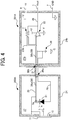
- FIG. 4 is a schematic view of a measuring apparatus 200A and an amplifying apparatus 201A.
- An offset may be provided between the guard ring 23, the housing 24, the conductive part 12, and the ground by using a direct current (DC) voltage source 26.
- DC direct current
- Such a configuration holds the entire measuring system including the light receiving device 21 at a constant voltage with respect to the housing 24 and the ground. Since the electric resistance and impedance of air between the housing 24 and the guard ring 23 are much larger than the electric resistance of portions connected as a circuit, a common-mode noise current does not flow, preventing generation of noise voltage. Accordingly, measurement accuracy is enhanced.
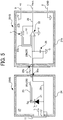
- FIG. 5 a description is given of a second variation of the measuring apparatus 200 and the amplifying apparatus 201 illustrated in FIG. 1 .
- FIG. 5 is a schematic view of a measuring apparatus 200B and an amplifying apparatus 201B.
- the guard ring 23, the housing 24, and the conductive part 12 are connected to each other via the DC voltage source 26.
- the DC voltage source 26 is disposed to offset the electric potentials of the guard ring 23 and a positive (+) side of the amplifier 22 from the ground.
- the disposition of the DC voltage source 26 is not limited thereto.
- Such a configuration holds the guard ring 23 at a constant voltage with respect to the housing 24 and the ground. In other words, a constant voltage is held between the guard ring 23 and the housing 24, and between the guard ring 23 and the ground. Therefore, a common-mode noise current does not flow to the guard ring 23, preventing generation of noise voltage. Accordingly, measurement accuracy is enhanced.
- Air resistance between the potential of the guard ring 23, the potential of the conductive part 12, and the potential of the housing 24 might generate a direct noise current.
- electrical resistance and impedance are much larger than the electrical resistance of portions connected as a circuit, and therefore a common-mode noise current does not flow, preventing generation of noise voltage. Accordingly, measurement accuracy is enhanced.
- a transparent conductive film may be used as the conductive part 12.
- FIG. 6 is a schematic view of the amplifying apparatus 201 and a measuring apparatus 200C incorporating a transparent conductive film 14 as an example of the conductive part 12 illustrated in FIG. 1 .
- the transparent conductive film 14 is disposed in contact with the surface of the optical window 11.
- Such a configuration reduces the number of manufacturing steps of the optical window 11 while facilitating electrostatic shielding with the housing 24 and the conductive part 12 of the optical window 11.
- FIG. 7 a description is given of a third variation of the measuring apparatus 200 and the amplifying apparatus 201 illustrated in FIG. 1 .
- FIG. 7 is a schematic view of a measuring apparatus 200D and an amplifying apparatus 201D.
- the amplifying apparatus 201 may include a buffer circuit 25.
- An input side of the buffer circuit 25 is connected to the electrical connection line 29b as a signal line.
- an output side of the buffer circuit 25 is connected to the guard ring 23b. Therefore, without affecting signals from the light receiving device 21, the buffer circuit 25 contributes to enhancement of the light receiving device 21 in response speed and in output dynamic range.
- the amplifying apparatus 201 is configured as an integrated part of the measuring apparatus (e.g., measuring apparatus 200).
- FIG. 8 is a schematic view of an integrated measuring apparatus 200E, as a fourth variation of the measuring apparatus 200 illustrated in FIG. 1 .
- FIG. 9 is a schematic view of an integrated measuring apparatus 200F, as a variation of the measuring apparatus 200A illustrated in FIG. 4 .
- FIG. 10 is a schematic view of an integrated measuring apparatus 200G, as a variation of the measuring apparatus 200B illustrated in FIG. 5 .
- FIG. 11 is a schematic view of an integrated measuring apparatus 200H, as a variation of the measuring apparatus 200C illustrated in FIG. 6 .
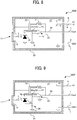
- FIG. 12 is a schematic view of an integrated measuring apparatus 2001, as a variation of the measuring apparatus 200D illustrated in FIG. 7 .
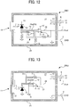
- FIG. 13 is a schematic view of an integrated measuring apparatus 200J, as a variation of the measuring apparatus 200E illustrated in FIG. 8 .
- FIG. 14 is a schematic view of an integrated measuring apparatus 200K, as another variation of the measuring apparatus 200E illustrated in FIG. 8 .
- the integrated measuring apparatuses 200E through 200K exclude the cable 31 and the external connectors 30a and 30b. Accordingly, the light receiving device 21 and the amplifier 22 are disposed closer to each other in the integrated measuring apparatuses 200E through 200K, compared to the measuring apparatuses 200 and 200A through 200D each being disposed independently from the amplifying apparatus 201. In other words, the amplifier 22 is connected to the light receiving device 21 via the electrical connection line 28a to amplify the electrical signal Sg output by the measuring apparatus 200. Therefore, the integrated measuring apparatuses 200E through 200K facilitates reduction of noise.
- the measuring apparatuses of the embodiments described above facilitates detection of weak light having a very low light intensity.
Landscapes
- Physics & Mathematics (AREA)
- General Physics & Mathematics (AREA)
- Spectroscopy & Molecular Physics (AREA)
- Chemical & Material Sciences (AREA)
- Biochemistry (AREA)
- Analytical Chemistry (AREA)
- General Health & Medical Sciences (AREA)
- Life Sciences & Earth Sciences (AREA)
- Immunology (AREA)
- Pathology (AREA)
- Health & Medical Sciences (AREA)
- Engineering & Computer Science (AREA)
- Radar, Positioning & Navigation (AREA)
- Computer Networks & Wireless Communication (AREA)
- Remote Sensing (AREA)
- Mathematical Physics (AREA)
- Chemical Kinetics & Catalysis (AREA)
- Plasma & Fusion (AREA)
- Measurement Of Radiation (AREA)
- Photometry And Measurement Of Optical Pulse Characteristics (AREA)
- Microelectronics & Electronic Packaging (AREA)
Abstract
Description
- Embodiments of the present disclosure relate to a measuring apparatus.
- Measurement of chemical substances using chemiluminescence or biochemical luminescence is proceeded in various fields because such measurement allows very low concentration measurement, specific measurement, and the like.
- In general, the light intensity of such chemiluminescence is relatively low. Therefore, there are strong demands for measuring apparatuses that detect weak light generated from light emitting substances.
- In light of such conventional circumstances, it is a general object of the present disclosure to provide a measuring apparatus for detecting light having a very low light intensity.
- In order to achieve the above-mentioned object, there is provided a measuring apparatus according to
claim 1. Advantageous embodiments are defined by the dependent claims. Advantageously, the measuring apparatus includes a light receiving device, a housing, an optical window, an electrical connection line, and a line enclosure. The light receiving device receives light and output a signal. The housing, made of a conductive material, covers the light receiving device. The optical window transmits the light. The optical window includes a conductive part having conductivity. The electrical connection line transmits the signal. The line enclosure is disposed around the electrical connection line and electrically connected to the conductive part and the housing. - Accordingly, the measuring apparatus facilitates detection of weak light having a very low light intensity.
- A more complete appreciation of the embodiments and many of the attendant advantages and features thereof can be readily obtained and understood from the following detailed description with reference to the accompanying drawings, wherein:
-
FIG. 1 is a schematic view of a measuring apparatus according to an embodiment of the present disclosure, with an amplifying apparatus; -
FIG. 2 is a schematic view of a comparative measuring apparatus with a comparative amplifying apparatus, simulating occurrence of common mode noise; -
FIG. 3A is a partial view of the measuring apparatus ofFIG. 1 , illustrating a guard ring surrounding an electrical connection line; -
FIG. 3B is a cross-sectional view of the guard ring surrounding the electrical connection line illustrated inFIG. 3A ; -
FIG. 4 is a schematic view of a first variation of the measuring apparatus and the amplifying apparatus illustrated inFIG. 1 ; -
FIG. 5 is a schematic view of a second variation of the measuring apparatus and the amplifying apparatus illustrated inFIG. 1 ; -
FIG. 6 is a schematic view of the amplifying apparatus and a measuring apparatus incorporating a transparent conductive film as an example of a conductive part illustrated inFIG. 1 ; -
FIG. 7 is a schematic view of a third variation of the measuring apparatus and the amplifying apparatus illustrated inFIG. 1 ; -
FIG. 8 is a schematic view of a fourth variation of the measuring apparatus illustrated inFIG. 1 ; -
FIG. 9 is a schematic view of a variation of the measuring apparatus illustrated inFIG. 4 ; -
FIG. 10 is a schematic view of a variation of the measuring apparatus illustrated inFIG. 5 ; -
FIG. 11 is a schematic view of a variation of the measuring apparatus illustrated inFIG. 6 ; -
FIG. 12 is a schematic view of a variation of the measuring apparatus illustrated inFIG. 7 ; -
FIG. 13 is a schematic view of a variation of the measuring apparatus illustrated inFIG. 8 ; and -
FIG. 14 is a schematic view of another variation of the measuring apparatus illustrated inFIG. 8 . - The accompanying drawings are intended to depict embodiments of the present disclosure and should not be interpreted to limit the scope thereof. Also, identical or similar reference numerals designate identical or similar components throughout the several views.
- In describing embodiments illustrated in the drawings, specific terminology is employed for the sake of clarity. However, the disclosure of the present specification is not intended to be limited to the specific terminology so selected and it is to be understood that each specific element includes all technical equivalents that have a similar function, operate in a similar manner, and achieve a similar result.
- Although the embodiments are described with technical limitations with reference to the attached drawings, such description is not intended to limit the scope of the disclosure and not all of the components or elements described in the embodiments of the present disclosure are indispensable to the present disclosure.
- In a later-described comparative example, embodiment, and exemplary variation, for the sake of simplicity like reference numerals are given to identical or corresponding constituent elements such as parts and materials having the same functions, and redundant descriptions thereof are omitted unless otherwise required.
- As used herein, the singular forms "a", "an", and "the" are intended to include the plural forms as well, unless the context clearly indicates otherwise.
- Referring to the drawings, wherein like reference numerals designate identical or corresponding parts throughout the several views, embodiments of the present disclosure are described below.
- Initially with reference to
FIG. 1 , a description is given of ameasuring apparatus 200 according to an embodiment of the present disclosure. -
FIG. 1 is a schematic view of themeasuring apparatus 200 with anamplifying apparatus 201. - The
measuring apparatus 200 includes, e.g., alight receiving device 21, ahousing 24, and anoptical window 11. Thelight receiving device 21 receives weak detection light L and generates a signal. Thehousing 24 is made of a conductive material to cover at least thelight receiving device 21. - The
optical window 11 is disposed as a part of thehousing 24 to transmit the detection light L. Theoptical window 11 includes aconductive part 12 having conductivity. - The
measuring apparatus 200 further includes anexternal connector 30a, aguard ring 23, andelectrical connection lines 28 such as electrical wires and cables that electrically connect components. Theexternal connector 30a is connected to thelight receiving device 21 via theelectrical connection line 28. Theguard ring 23 is disposed around anelectrical connection line 28a as a signal line, thereby serving as a line enclosure. - As illustrated in
FIG. 1 , acable 31 couples themeasuring apparatus 200 to the amplifyingapparatus 201. - The
light receiving device 21 is an element that outputs an electrical signal Sg upon reception of the detection light L. Examples of thelight receiving device 21 include a photodiode, a phototransistor, and a photo integrated circuit (IC). - The
housing 24 is a conductive metal material disposed to cover at least thelight receiving device 21. - Although the
housing 24 is a metal box in the present embodiment, thehousing 24 is not particularly limited to a metal provided that thehousing 24 is a material having conductivity. - The
optical window 11 is made of glass, resin, or the like spanning an opening of thehousing 24 as illustrated inFIG. 1 , so as to transmit the detection light L. An indium tin oxide (ITO) film is vapor-deposited on a surface of theoptical window 11. In other words, theoptical window 11 has a surface provided with theconductive part 12 that is a portion subjected to a conductive treatment. - Note that the
housing 24 and theconductive part 12 are electrically connected to each other at identical electric potentials. - The
conductive part 12 is the ITO film vapor-deposited on the surface of theoptical window 11. Theconductive part 12 has conductivity and good transparency with respect to a wavelength band of the detection light L. That is, theconductive part 12 transmits the detection light L. - With such a configuration, the
conductive part 12 is electrically connected to thehousing 24 without disturbing the weak detection light L. Consequently, the measuringapparatus 200 is covered with grounds of identical electric potentials, thereby reducing noise due to the influence from outside. Note that the measuringapparatus 200 may be covered with any other forms of identical electric potentials. - With the conductive treatment such as vapor deposition, the present embodiment reduces the number of parts.
- In addition, even if the
optical window 11 has a special shape such as a lens shape, the conductive treatment prevents distortion of theoptical window 11, thereby retaining a suitable shape of theoptical window 11. - Note that, in the present embodiment, the conductive treatment includes vapor-deposition of the ITO film, but is not limited thereto. Alternatively, the conductive treatment may include vapor-deposition of a transparent conductive film such as fluorine doped tin oxide (FTO), antimony doped tin oxide (ATO), or gallium-doped zinc oxide (GZO).
- In the present embodiment, the
conductive part 12 is the ITO film vapor-deposited on the surface of theoptical window 11. Alternatively, a transparent conductive sheet or film, such as ST-PET (registered trademark) transparent conductive sheet made by Achilles Corporation or a carbon nanotube (CNT) film made by Toray Industries, Inc., may be disposed in contact with the surface of theoptical window 11 as theconductive part 12. - Using such a transparent conductive film as the
conductive part 12 reduces the number of man-hours for conductive treatment of theoptical window 11 and facilitates covering of theoptical window 11 spanning the opening of thehousing 24, with a conductive material. - In the present embodiment, the
electrical connection lines 28 are disposed on acircuit board 27 on which thelight receiving device 21 is disposed. - The
external connector 30a is coupled to thecable 31 that transmits the electrical signal Sg from thelight receiving device 21 to theamplifying apparatus 201. In the present example, theexternal connector 30a is a triaxial connector. - As illustrated in
FIG. 1 , the measuringapparatus 200 is coupled to thecable 31 via theexternal connector 30a. Alternatively, for example, thecable 31 may be directly coupled to thecircuit board 27 of the measuringapparatus 200. - The amplifying
apparatus 201 includes anexternal connector 30b, anamplifier 22, ahousing 24b, aguard ring 23b, andelectrical connection lines 29 such as electrical wires and cables that electrically connect components. Theamplifier 22 is connected to theexternal connector 30b via theelectrical connection line 29 to amplify the electrical signal Sg output by the measuringapparatus 200. Thehousing 24b is made of a conductive material to cover at least theamplifier 22. Theguard ring 23b is disposed around anelectrical connection line 29b as a signal line, thereby serving as a line enclosure. Theexternal connector 30b is coupled to thecable 31 that transmits the electrical signal Sg output from the measuringapparatus 200 to theamplifying apparatus 201. In the present example, theexternal connector 30b is a triaxial connector. - As illustrated in
FIG. 1 , the amplifyingapparatus 201 is coupled to thecable 31 via theexternal connector 30b. Alternatively, for example, thecable 31 may be directly coupled to acircuit board 27b of the amplifyingapparatus 201. - In the present embodiment, the
electrical connection lines 29 are disposed on thecircuit board 27b on which theamplifier 22 is disposed. - In the present embodiment, the
amplifier 22 is an operational amplifier. Upon receiving the electrical signal Sg from thelight receiving device 21, theamplifier 22 amplifies the electrical signal Sg according to a current-voltage (I/V)conversion resistor 7. - In the present embodiment, the
amplifier 22 is capable of amplifying the electrical signal Sg about 109 times. - The
housing 24b is a conductive metal material disposed to cover at least theamplifier 22. Although thehousing 24b is a metal box in the present embodiment, thehousing 24b is not particularly limited to a metal provided that thehousing 24b is a material having conductivity. - The
cable 31 produces substantially the same effect as surrounding or enclosing a signal line with a guard ring. In the present example, thecable 31 is a triaxial connector. - In the measuring
apparatus 200, theguard ring 23 is a surround or an enclosure made of a conductive material and disposed around theelectrical connection line 28a. Theguard ring 23 surrounds at least theelectrical connection line 28a of the electrical connection lines 28. Theelectrical connection line 28a connects thelight receiving device 21 and theexternal connector 30a. That is, in the present embodiment, theguard ring 23 serves as a line enclosure. - Similarly, in the
amplifying apparatus 201, theguard ring 23b surrounds theelectrical connection line 29b that connects theexternal connector 30b and theamplifier 22. - In other words, the
guard ring 23 is disposed around theelectrical connection line 28a as a signal line so as to reduce leakage current from theelectrical connection line 28a to the surroundings. Similarly, theguard ring 23b is disposed around theelectrical connection line 29b as a signal line so as to reduce leakage current from theelectrical connection line 29b to the surroundings. Specifically, the guard rings 23 and 23b surround, in a plane, theelectrical connection lines 28a and 29a, respectively, on a surface of therespective circuit boards - The guard rings 23 and 23b are conductive lines such as wires or cables made of substantially the same material as the material of the
electrical connection lines - In the measuring
apparatus 200, theguard ring 23 is electrically connected to thehousing 24 and theconductive part 12 at identical electric potentials. In other words, theconductive part 12, thehousing 24, and theguard ring 23 have identical electric potentials. - The
guard ring 23 may be electrically connected to thehousing 24 and theconductive part 12 via a ground G, which is a reference potential illustrated as an inverted triangle inFIG. 1 . - A description is now given of how to reduce noise with the
guard ring 23 described above. - Typically, a large number of noise sources for weak current signals are known such as superimposition on the signals by electrostatic induction from outside.
- In order to suppress such disturbance from outside, electrostatic shielding is well known. For example, by grounding the surroundings of a signal line, a shielded cable electrostatically shields the signal line, thereby reducing noise caused by electrostatic induction.
-
FIG. 2 is a schematic view of acomparative measuring apparatus 1200 with acomparative amplifying apparatus 1201, simulating occurrence of common mode noise. - For example, simply grounding
housings FIG. 2 by using conventional technique may not prevent a common-mode noise current 4 from being generated inelectrical connection lines - A stray capacitance C (i.e.,
stray capacitance 5 inFIG. 2 ) between alight receiving device 121 and thehousing 124 as an electrostatic shield and an air resistance R (i.e., impedance 6 inFIG. 2 ) generate a loop of the common-mode noise current 4 that commonly flows throughelectrical connection lines FIG. 2 . - Since such a loop of the electric current via the ground is generated involving the
electrical connection lines - Normally, the stray capacitance (i.e.,
stray capacitance 5 inFIG. 2 ) between thelight receiving device 121 and thehousing 124 or a stray capacitance between the ground and theelectrical connection lines - Note that the flow of the common-mode noise current 4 as described above is an example of a noise generation mechanism. There are other paths where noise occurs.
- In order to reduce such common mode noise, a circuit is to be prepared while preventing the
electrical connection line 28a as a signal line from being a flow path of the common-mode noise current 4. - That is, the
guard ring 23 surrounds at least theelectrical connection line 28a to prevent leakage current to the surroundings on the surface of thecircuit board 27. In addition, theguard ring 23 is electrically connected to thehousing 24 and theconductive part 12, thereby being equal in electric potential to thehousing 24. As a consequence, the stray capacitance is further reduced. - Since a common-mode noise current passes through a path having the lowest impedance, the leakage current tends to flow most on the surface of the
circuit board 27. -
FIG. 3A is a partial view of the measuringapparatus 200 ofFIG. 1 , illustrating theguard ring 23 surrounding theelectrical connection line 28a.FIG. 3B is a cross-sectional view of theguard ring 23 surrounding theelectrical connection line 28a illustrated inFIG. 3A , along a line AA. - In order to prevent such leakage current, in the present embodiment, the
guard ring 23 is disposed to surround the electrical connection line in a plane on the surface of thecircuit board 27 as illustrated inFIGs. 3A and 3B . - Alternatively, for example, the
guard ring 23 may surround theelectrical connection line 28a, regarded as a shielded signal line, not only in a plane on the surface of thecircuit board 27 but also in a depth direction (i.e., height direction) of thecircuit board 27. - Even when the common-mode noise current is generated by, e.g., induction from outside as the
guard ring 23 is electrically connected to thehousing 24 and theconductive part 12 of theoptical window 11, the current flows to theguard ring 23, thereby ending the loop. Accordingly, the influence of noise on theelectrical connection line 28a is reduced. - Thus, the
guard ring 23 disposed around theelectrical connection line 28a and connected to the grounds suppresses the influence on the signals passing though theelectrical connection line 28a, even when the common-mode noise current is generated. - With such a configuration, the measuring
apparatus 200 accurately detects weak light having a very low light intensity. - Further, in the present embodiment, the
optical window 11 spanning the opening of thehousing 24 includes theconductive part 12. Theconductive part 12, thehousing 24, and theguard ring 23 are electrically connected to each other. With such a configuration, theentire housing 24 has an electrostatic shielding effect against disturbance. Accordingly, the measuringapparatus 200 of the present embodiment accurately detects weak light having a very low light intensity while effectively reducing noise. - A description is now given of variations of the measuring
apparatus 200 and the amplifyingapparatus 201 described above. - Initially with reference to
FIG. 4 , a description is now given of a first variation of the measuringapparatus 200 and the amplifyingapparatus 201 illustrated inFIG. 1 . -
FIG. 4 is a schematic view of a measuringapparatus 200A and anamplifying apparatus 201A. - An offset may be provided between the
guard ring 23, thehousing 24, theconductive part 12, and the ground by using a direct current (DC)voltage source 26. - Such a configuration holds the entire measuring system including the
light receiving device 21 at a constant voltage with respect to thehousing 24 and the ground. Since the electric resistance and impedance of air between thehousing 24 and theguard ring 23 are much larger than the electric resistance of portions connected as a circuit, a common-mode noise current does not flow, preventing generation of noise voltage. Accordingly, measurement accuracy is enhanced. - There is also an advantage that the
amplifier 22 is driven by a single power supply. - Referring now to
FIG. 5 , a description is given of a second variation of the measuringapparatus 200 and the amplifyingapparatus 201 illustrated inFIG. 1 . -
FIG. 5 is a schematic view of a measuringapparatus 200B and anamplifying apparatus 201B. - In
FIG. 5 , theguard ring 23, thehousing 24, and theconductive part 12 are connected to each other via theDC voltage source 26. - Note that, in the present variation, the
DC voltage source 26 is disposed to offset the electric potentials of theguard ring 23 and a positive (+) side of theamplifier 22 from the ground. The disposition of theDC voltage source 26 is not limited thereto. - Such a configuration holds the
guard ring 23 at a constant voltage with respect to thehousing 24 and the ground. In other words, a constant voltage is held between theguard ring 23 and thehousing 24, and between theguard ring 23 and the ground. Therefore, a common-mode noise current does not flow to theguard ring 23, preventing generation of noise voltage. Accordingly, measurement accuracy is enhanced. - Air resistance between the potential of the
guard ring 23, the potential of theconductive part 12, and the potential of thehousing 24 might generate a direct noise current. However, such electrical resistance and impedance are much larger than the electrical resistance of portions connected as a circuit, and therefore a common-mode noise current does not flow, preventing generation of noise voltage. Accordingly, measurement accuracy is enhanced. - With respect to the
conductive part 12, a transparent conductive film may be used as theconductive part 12. - Referring now to
FIG. 6 , a description is given of an example of theconductive part 12. -
FIG. 6 is a schematic view of the amplifyingapparatus 201 and a measuringapparatus 200C incorporating a transparentconductive film 14 as an example of theconductive part 12 illustrated inFIG. 1 . - As illustrated in
FIG. 6 , the transparentconductive film 14 is disposed in contact with the surface of theoptical window 11. - Such a configuration reduces the number of manufacturing steps of the
optical window 11 while facilitating electrostatic shielding with thehousing 24 and theconductive part 12 of theoptical window 11. - Referring now to
FIG. 7 , a description is given of a third variation of the measuringapparatus 200 and the amplifyingapparatus 201 illustrated inFIG. 1 . -
FIG. 7 is a schematic view of ameasuring apparatus 200D and anamplifying apparatus 201D. - The amplifying
apparatus 201 may include abuffer circuit 25. - An input side of the
buffer circuit 25 is connected to theelectrical connection line 29b as a signal line. On the other hand, an output side of thebuffer circuit 25 is connected to theguard ring 23b. Therefore, without affecting signals from thelight receiving device 21, thebuffer circuit 25 contributes to enhancement of thelight receiving device 21 in response speed and in output dynamic range. - Referring now to
FIGs. 8 through 14 , a description is given of a configuration in which theamplifying apparatus 201 is configured as an integrated part of the measuring apparatus (e.g., measuring apparatus 200). - Specifically,
FIG. 8 is a schematic view of anintegrated measuring apparatus 200E, as a fourth variation of the measuringapparatus 200 illustrated inFIG. 1 .FIG. 9 is a schematic view of anintegrated measuring apparatus 200F, as a variation of the measuringapparatus 200A illustrated inFIG. 4 .FIG. 10 is a schematic view of anintegrated measuring apparatus 200G, as a variation of the measuringapparatus 200B illustrated inFIG. 5 .FIG. 11 is a schematic view of anintegrated measuring apparatus 200H, as a variation of the measuringapparatus 200C illustrated inFIG. 6 .FIG. 12 is a schematic view of anintegrated measuring apparatus 2001, as a variation of the measuringapparatus 200D illustrated inFIG. 7 .FIG. 13 is a schematic view of anintegrated measuring apparatus 200J, as a variation of the measuringapparatus 200E illustrated inFIG. 8 .FIG. 14 is a schematic view of anintegrated measuring apparatus 200K, as another variation of the measuringapparatus 200E illustrated inFIG. 8 . - The
integrated measuring apparatuses 200E through 200K exclude thecable 31 and theexternal connectors light receiving device 21 and theamplifier 22 are disposed closer to each other in theintegrated measuring apparatuses 200E through 200K, compared to the measuringapparatuses apparatus 201. In other words, theamplifier 22 is connected to thelight receiving device 21 via theelectrical connection line 28a to amplify the electrical signal Sg output by the measuringapparatus 200. Therefore, theintegrated measuring apparatuses 200E through 200K facilitates reduction of noise. - Accordingly, the measuring apparatuses of the embodiments described above facilitates detection of weak light having a very low light intensity.
Claims (7)
- A measuring apparatus (200) comprising:a light receiving device (21) to receive light and output a signal;a housing (24), made of a conductive material, to cover the light receiving device (21);an optical window (11) to transmit the light, the optical window (11) including a conductive part (12) having conductivity;an electrical connection line (28a) to transmit the signal; anda line enclosure (23) disposed around the electrical connection line (28a) and electrically connected to the conductive part (12) and the housing (24).
- The measuring apparatus (200) according to claim 1, further comprising an amplifier (22) connected to the light receiving device (21) via the electrical connection line (28a) to amplify the signal output by the light receiving device (21).
- The measuring apparatus (200) according to claim 1 or 2,
wherein the conductive part (12), the housing (24), and the line enclosure (23) have identical electric potentials. - The measuring apparatus (200) according to any one of claims 1 to 3,
wherein the conductive part (12) includes a portion of the optical window (11) subjected to a conductive treatment. - The measuring apparatus (200) according to any one of claims 1 to 3,
wherein the conductive part (12) includes a conductive film (14) disposed in contact with the optical window (11). - The measuring apparatus (200) according to any one of claims 1 to 5, further comprising a ground (G),
wherein the conductive part (12), the housing (24), and the line enclosure (23) are connected to the ground (G). - The measuring apparatus (200) according to any one of claims 1 to 5, further comprising a ground (G),
wherein the housing (24) and the conductive part (12) are connected to the ground (G) to maintain a constant voltage between the line enclosure (23) and the ground (G).
Applications Claiming Priority (2)
| Application Number | Priority Date | Filing Date | Title |
|---|---|---|---|
| JP2017155413 | 2017-08-10 | ||
| JP2018121956A JP2019036715A (en) | 2017-08-10 | 2018-06-27 | Measuring apparatus |
Publications (2)
| Publication Number | Publication Date |
|---|---|
| EP3441730A1 true EP3441730A1 (en) | 2019-02-13 |
| EP3441730B1 EP3441730B1 (en) | 2020-10-21 |
Family
ID=63041803
Family Applications (1)
| Application Number | Title | Priority Date | Filing Date |
|---|---|---|---|
| EP18184817.7A Not-in-force EP3441730B1 (en) | 2017-08-10 | 2018-07-20 | Light measuring apparatus |
Country Status (3)
| Country | Link |
|---|---|
| US (1) | US10670532B2 (en) |
| EP (1) | EP3441730B1 (en) |
| CN (1) | CN109387502B (en) |
Families Citing this family (1)
| Publication number | Priority date | Publication date | Assignee | Title |
|---|---|---|---|---|
| CN113533219B (en) * | 2020-04-17 | 2026-04-07 | 深圳迈瑞生物医疗电子股份有限公司 | Measuring apparatus for sample testing and its installation method |
Citations (2)
| Publication number | Priority date | Publication date | Assignee | Title |
|---|---|---|---|---|
| JPH08172248A (en) * | 1994-12-20 | 1996-07-02 | Nikon Corp | Printed board |
| JP2010276407A (en) * | 2009-05-27 | 2010-12-09 | Spectratech Inc | Photodetection device and biological information measurement device |
Family Cites Families (12)
| Publication number | Priority date | Publication date | Assignee | Title |
|---|---|---|---|---|
| US4441023A (en) * | 1981-07-29 | 1984-04-03 | Eltec Instruments, Inc. | High output differential pyroelectric sensor |
| JPH05133892A (en) | 1991-11-14 | 1993-05-28 | Ricoh Co Ltd | Toner concentration sensor |
| JP3559998B2 (en) | 1994-06-28 | 2004-09-02 | 株式会社堀場製作所 | Chemiluminescence analyzer |
| JP4410900B2 (en) | 2000-02-29 | 2010-02-03 | 東亜ディーケーケー株式会社 | Luminescence detector |
| JP2004012411A (en) * | 2002-06-11 | 2004-01-15 | Hitachi Ltd | Emission detection device |
| CN101361191A (en) * | 2006-01-24 | 2009-02-04 | 株式会社理光 | Electronic components, current control devices, computing devices and display devices |
| CN1971245A (en) * | 2006-12-12 | 2007-05-30 | 冶金自动化研究设计院 | A measuring device for weak light photons |
| CN100494989C (en) * | 2007-01-11 | 2009-06-03 | 山西大学 | Method and device for measuring weak fluorescence spectrum |
| CN101718680B (en) * | 2009-11-26 | 2011-04-06 | 西南科技大学 | Photoacoustic gas detecting method and photoacoustic gas detecting device capable of reducing environmental noise |
| JP5834494B2 (en) * | 2011-05-27 | 2015-12-24 | 三菱電機株式会社 | Optical receiver |
| CN102967566A (en) * | 2012-11-14 | 2013-03-13 | 广东汉唐量子光电科技有限公司 | A high-precision rapid trace analysis device |
| JP6607678B2 (en) | 2015-02-10 | 2019-11-20 | 株式会社リコー | Urea concentration measuring method and urea concentration measuring device |
-
2018
- 2018-07-20 EP EP18184817.7A patent/EP3441730B1/en not_active Not-in-force
- 2018-08-01 CN CN201810859908.6A patent/CN109387502B/en not_active Expired - Fee Related
- 2018-08-07 US US16/057,065 patent/US10670532B2/en not_active Expired - Fee Related
Patent Citations (2)
| Publication number | Priority date | Publication date | Assignee | Title |
|---|---|---|---|---|
| JPH08172248A (en) * | 1994-12-20 | 1996-07-02 | Nikon Corp | Printed board |
| JP2010276407A (en) * | 2009-05-27 | 2010-12-09 | Spectratech Inc | Photodetection device and biological information measurement device |
Also Published As
| Publication number | Publication date |
|---|---|
| CN109387502B (en) | 2021-12-24 |
| CN109387502A (en) | 2019-02-26 |
| US20190049389A1 (en) | 2019-02-14 |
| US10670532B2 (en) | 2020-06-02 |
| EP3441730B1 (en) | 2020-10-21 |
Similar Documents
| Publication | Publication Date | Title |
|---|---|---|
| US10797388B2 (en) | Vehicle-mounted antenna device | |
| US5499281A (en) | Apparatus for shielding and grounding x-ray detectors of a CT scanner | |
| CN104121933B (en) | Rotary encoder | |
| CN211744554U (en) | Camera with a camera module | |
| EP3441730B1 (en) | Light measuring apparatus | |
| JP5355940B2 (en) | Radiation detector | |
| TW201714056A (en) | Touch sensing module and touch sensing display apparatus with the same | |
| CN110353708B (en) | Radiation imaging apparatus | |
| CN1303399C (en) | Detection system | |
| CN112087850B (en) | Light sensing module and electronic equipment | |
| CN105708483B (en) | Radiation detection apparatus and radiation imaging system | |
| JP2019036715A (en) | Measuring apparatus | |
| US7897913B2 (en) | Image sensing device having a shielding layer | |
| TWI506323B (en) | Photoelectric module | |
| US11968849B2 (en) | Radiation detector | |
| CN223402670U (en) | Flat panel detectors and testing equipment | |
| CN113056804B (en) | sensor | |
| JP2016197497A (en) | Operation detector | |
| JPH0365604A (en) | Optical sensor device | |
| CN112834489A (en) | A single photon counting device for chemiluminescence | |
| CN210293989U (en) | Laser dust detection device and laser dust detection mechanism | |
| US2345501A (en) | High gain amplifier | |
| CN111511068A (en) | Chip type photoelectric sensor and gesture recognition device | |
| US20250237744A1 (en) | Attenuation wall to reduce optical noise in an optical ranging sensor | |
| CN112987071B (en) | Sensors for X-ray machines that detect static electricity |
Legal Events
| Date | Code | Title | Description |
|---|---|---|---|
| PUAI | Public reference made under article 153(3) epc to a published international application that has entered the european phase |
Free format text: ORIGINAL CODE: 0009012 |
|
| STAA | Information on the status of an ep patent application or granted ep patent |
Free format text: STATUS: REQUEST FOR EXAMINATION WAS MADE |
|
| 17P | Request for examination filed |
Effective date: 20180720 |
|
| AK | Designated contracting states |
Kind code of ref document: A1 Designated state(s): AL AT BE BG CH CY CZ DE DK EE ES FI FR GB GR HR HU IE IS IT LI LT LU LV MC MK MT NL NO PL PT RO RS SE SI SK SM TR |
|
| AX | Request for extension of the european patent |
Extension state: BA ME |
|
| GRAP | Despatch of communication of intention to grant a patent |
Free format text: ORIGINAL CODE: EPIDOSNIGR1 |
|
| STAA | Information on the status of an ep patent application or granted ep patent |
Free format text: STATUS: GRANT OF PATENT IS INTENDED |
|
| INTG | Intention to grant announced |
Effective date: 20200713 |
|
| RAP1 | Party data changed (applicant data changed or rights of an application transferred) |
Owner name: RICOH COMPANY, LTD. |
|
| GRAS | Grant fee paid |
Free format text: ORIGINAL CODE: EPIDOSNIGR3 |
|
| GRAA | (expected) grant |
Free format text: ORIGINAL CODE: 0009210 |
|
| STAA | Information on the status of an ep patent application or granted ep patent |
Free format text: STATUS: THE PATENT HAS BEEN GRANTED |
|
| AK | Designated contracting states |
Kind code of ref document: B1 Designated state(s): AL AT BE BG CH CY CZ DE DK EE ES FI FR GB GR HR HU IE IS IT LI LT LU LV MC MK MT NL NO PL PT RO RS SE SI SK SM TR |
|
| REG | Reference to a national code |
Ref country code: GB Ref legal event code: FG4D |
|
| REG | Reference to a national code |
Ref country code: CH Ref legal event code: EP |
|
| REG | Reference to a national code |
Ref country code: IE Ref legal event code: FG4D |
|
| REG | Reference to a national code |
Ref country code: DE Ref legal event code: R096 Ref document number: 602018008856 Country of ref document: DE |
|
| REG | Reference to a national code |
Ref country code: AT Ref legal event code: REF Ref document number: 1326290 Country of ref document: AT Kind code of ref document: T Effective date: 20201115 |
|
| REG | Reference to a national code |
Ref country code: AT Ref legal event code: MK05 Ref document number: 1326290 Country of ref document: AT Kind code of ref document: T Effective date: 20201021 |
|
| REG | Reference to a national code |
Ref country code: NL Ref legal event code: MP Effective date: 20201021 |
|
| PG25 | Lapsed in a contracting state [announced via postgrant information from national office to epo] |
Ref country code: PT Free format text: LAPSE BECAUSE OF FAILURE TO SUBMIT A TRANSLATION OF THE DESCRIPTION OR TO PAY THE FEE WITHIN THE PRESCRIBED TIME-LIMIT Effective date: 20210222 Ref country code: RS Free format text: LAPSE BECAUSE OF FAILURE TO SUBMIT A TRANSLATION OF THE DESCRIPTION OR TO PAY THE FEE WITHIN THE PRESCRIBED TIME-LIMIT Effective date: 20201021 Ref country code: FI Free format text: LAPSE BECAUSE OF FAILURE TO SUBMIT A TRANSLATION OF THE DESCRIPTION OR TO PAY THE FEE WITHIN THE PRESCRIBED TIME-LIMIT Effective date: 20201021 Ref country code: NO Free format text: LAPSE BECAUSE OF FAILURE TO SUBMIT A TRANSLATION OF THE DESCRIPTION OR TO PAY THE FEE WITHIN THE PRESCRIBED TIME-LIMIT Effective date: 20210121 Ref country code: GR Free format text: LAPSE BECAUSE OF FAILURE TO SUBMIT A TRANSLATION OF THE DESCRIPTION OR TO PAY THE FEE WITHIN THE PRESCRIBED TIME-LIMIT Effective date: 20210122 |
|
| REG | Reference to a national code |
Ref country code: LT Ref legal event code: MG4D |
|
| PG25 | Lapsed in a contracting state [announced via postgrant information from national office to epo] |
Ref country code: BG Free format text: LAPSE BECAUSE OF FAILURE TO SUBMIT A TRANSLATION OF THE DESCRIPTION OR TO PAY THE FEE WITHIN THE PRESCRIBED TIME-LIMIT Effective date: 20210121 Ref country code: PL Free format text: LAPSE BECAUSE OF FAILURE TO SUBMIT A TRANSLATION OF THE DESCRIPTION OR TO PAY THE FEE WITHIN THE PRESCRIBED TIME-LIMIT Effective date: 20201021 Ref country code: IS Free format text: LAPSE BECAUSE OF FAILURE TO SUBMIT A TRANSLATION OF THE DESCRIPTION OR TO PAY THE FEE WITHIN THE PRESCRIBED TIME-LIMIT Effective date: 20210221 Ref country code: LV Free format text: LAPSE BECAUSE OF FAILURE TO SUBMIT A TRANSLATION OF THE DESCRIPTION OR TO PAY THE FEE WITHIN THE PRESCRIBED TIME-LIMIT Effective date: 20201021 Ref country code: SE Free format text: LAPSE BECAUSE OF FAILURE TO SUBMIT A TRANSLATION OF THE DESCRIPTION OR TO PAY THE FEE WITHIN THE PRESCRIBED TIME-LIMIT Effective date: 20201021 Ref country code: AT Free format text: LAPSE BECAUSE OF FAILURE TO SUBMIT A TRANSLATION OF THE DESCRIPTION OR TO PAY THE FEE WITHIN THE PRESCRIBED TIME-LIMIT Effective date: 20201021 Ref country code: ES Free format text: LAPSE BECAUSE OF FAILURE TO SUBMIT A TRANSLATION OF THE DESCRIPTION OR TO PAY THE FEE WITHIN THE PRESCRIBED TIME-LIMIT Effective date: 20201021 |
|
| PG25 | Lapsed in a contracting state [announced via postgrant information from national office to epo] |
Ref country code: HR Free format text: LAPSE BECAUSE OF FAILURE TO SUBMIT A TRANSLATION OF THE DESCRIPTION OR TO PAY THE FEE WITHIN THE PRESCRIBED TIME-LIMIT Effective date: 20201021 Ref country code: NL Free format text: LAPSE BECAUSE OF FAILURE TO SUBMIT A TRANSLATION OF THE DESCRIPTION OR TO PAY THE FEE WITHIN THE PRESCRIBED TIME-LIMIT Effective date: 20201021 |
|
| REG | Reference to a national code |
Ref country code: DE Ref legal event code: R097 Ref document number: 602018008856 Country of ref document: DE |
|
| PG25 | Lapsed in a contracting state [announced via postgrant information from national office to epo] |
Ref country code: LT Free format text: LAPSE BECAUSE OF FAILURE TO SUBMIT A TRANSLATION OF THE DESCRIPTION OR TO PAY THE FEE WITHIN THE PRESCRIBED TIME-LIMIT Effective date: 20201021 Ref country code: RO Free format text: LAPSE BECAUSE OF FAILURE TO SUBMIT A TRANSLATION OF THE DESCRIPTION OR TO PAY THE FEE WITHIN THE PRESCRIBED TIME-LIMIT Effective date: 20201021 Ref country code: SK Free format text: LAPSE BECAUSE OF FAILURE TO SUBMIT A TRANSLATION OF THE DESCRIPTION OR TO PAY THE FEE WITHIN THE PRESCRIBED TIME-LIMIT Effective date: 20201021 Ref country code: CZ Free format text: LAPSE BECAUSE OF FAILURE TO SUBMIT A TRANSLATION OF THE DESCRIPTION OR TO PAY THE FEE WITHIN THE PRESCRIBED TIME-LIMIT Effective date: 20201021 Ref country code: EE Free format text: LAPSE BECAUSE OF FAILURE TO SUBMIT A TRANSLATION OF THE DESCRIPTION OR TO PAY THE FEE WITHIN THE PRESCRIBED TIME-LIMIT Effective date: 20201021 Ref country code: SM Free format text: LAPSE BECAUSE OF FAILURE TO SUBMIT A TRANSLATION OF THE DESCRIPTION OR TO PAY THE FEE WITHIN THE PRESCRIBED TIME-LIMIT Effective date: 20201021 |
|
| PLBE | No opposition filed within time limit |
Free format text: ORIGINAL CODE: 0009261 |
|
| STAA | Information on the status of an ep patent application or granted ep patent |
Free format text: STATUS: NO OPPOSITION FILED WITHIN TIME LIMIT |
|
| PG25 | Lapsed in a contracting state [announced via postgrant information from national office to epo] |
Ref country code: DK Free format text: LAPSE BECAUSE OF FAILURE TO SUBMIT A TRANSLATION OF THE DESCRIPTION OR TO PAY THE FEE WITHIN THE PRESCRIBED TIME-LIMIT Effective date: 20201021 |
|
| 26N | No opposition filed |
Effective date: 20210722 |
|
| PG25 | Lapsed in a contracting state [announced via postgrant information from national office to epo] |
Ref country code: IT Free format text: LAPSE BECAUSE OF FAILURE TO SUBMIT A TRANSLATION OF THE DESCRIPTION OR TO PAY THE FEE WITHIN THE PRESCRIBED TIME-LIMIT Effective date: 20201021 Ref country code: AL Free format text: LAPSE BECAUSE OF FAILURE TO SUBMIT A TRANSLATION OF THE DESCRIPTION OR TO PAY THE FEE WITHIN THE PRESCRIBED TIME-LIMIT Effective date: 20201021 |
|
| PGFP | Annual fee paid to national office [announced via postgrant information from national office to epo] |
Ref country code: FR Payment date: 20210729 Year of fee payment: 4 |
|
| PG25 | Lapsed in a contracting state [announced via postgrant information from national office to epo] |
Ref country code: SI Free format text: LAPSE BECAUSE OF FAILURE TO SUBMIT A TRANSLATION OF THE DESCRIPTION OR TO PAY THE FEE WITHIN THE PRESCRIBED TIME-LIMIT Effective date: 20201021 |
|
| PGFP | Annual fee paid to national office [announced via postgrant information from national office to epo] |
Ref country code: DE Payment date: 20210721 Year of fee payment: 4 |
|
| REG | Reference to a national code |
Ref country code: CH Ref legal event code: PL |
|
| PG25 | Lapsed in a contracting state [announced via postgrant information from national office to epo] |
Ref country code: MC Free format text: LAPSE BECAUSE OF FAILURE TO SUBMIT A TRANSLATION OF THE DESCRIPTION OR TO PAY THE FEE WITHIN THE PRESCRIBED TIME-LIMIT Effective date: 20201021 |
|
| REG | Reference to a national code |
Ref country code: BE Ref legal event code: MM Effective date: 20210731 |
|
| PG25 | Lapsed in a contracting state [announced via postgrant information from national office to epo] |
Ref country code: LI Free format text: LAPSE BECAUSE OF NON-PAYMENT OF DUE FEES Effective date: 20210731 Ref country code: CH Free format text: LAPSE BECAUSE OF NON-PAYMENT OF DUE FEES Effective date: 20210731 |
|
| PG25 | Lapsed in a contracting state [announced via postgrant information from national office to epo] |
Ref country code: IS Free format text: LAPSE BECAUSE OF FAILURE TO SUBMIT A TRANSLATION OF THE DESCRIPTION OR TO PAY THE FEE WITHIN THE PRESCRIBED TIME-LIMIT Effective date: 20210221 Ref country code: LU Free format text: LAPSE BECAUSE OF NON-PAYMENT OF DUE FEES Effective date: 20210720 |
|
| PG25 | Lapsed in a contracting state [announced via postgrant information from national office to epo] |
Ref country code: IE Free format text: LAPSE BECAUSE OF NON-PAYMENT OF DUE FEES Effective date: 20210720 Ref country code: BE Free format text: LAPSE BECAUSE OF NON-PAYMENT OF DUE FEES Effective date: 20210731 |
|
| REG | Reference to a national code |
Ref country code: DE Ref legal event code: R119 Ref document number: 602018008856 Country of ref document: DE |
|
| GBPC | Gb: european patent ceased through non-payment of renewal fee |
Effective date: 20220720 |
|
| PG25 | Lapsed in a contracting state [announced via postgrant information from national office to epo] |
Ref country code: FR Free format text: LAPSE BECAUSE OF NON-PAYMENT OF DUE FEES Effective date: 20220731 |
|
| PG25 | Lapsed in a contracting state [announced via postgrant information from national office to epo] |
Ref country code: GB Free format text: LAPSE BECAUSE OF NON-PAYMENT OF DUE FEES Effective date: 20220720 Ref country code: DE Free format text: LAPSE BECAUSE OF NON-PAYMENT OF DUE FEES Effective date: 20230201 |
|
| PG25 | Lapsed in a contracting state [announced via postgrant information from national office to epo] |
Ref country code: CY Free format text: LAPSE BECAUSE OF FAILURE TO SUBMIT A TRANSLATION OF THE DESCRIPTION OR TO PAY THE FEE WITHIN THE PRESCRIBED TIME-LIMIT Effective date: 20201021 |
|
| PG25 | Lapsed in a contracting state [announced via postgrant information from national office to epo] |
Ref country code: HU Free format text: LAPSE BECAUSE OF FAILURE TO SUBMIT A TRANSLATION OF THE DESCRIPTION OR TO PAY THE FEE WITHIN THE PRESCRIBED TIME-LIMIT; INVALID AB INITIO Effective date: 20180720 |
|
| PG25 | Lapsed in a contracting state [announced via postgrant information from national office to epo] |
Ref country code: MK Free format text: LAPSE BECAUSE OF FAILURE TO SUBMIT A TRANSLATION OF THE DESCRIPTION OR TO PAY THE FEE WITHIN THE PRESCRIBED TIME-LIMIT Effective date: 20201021 |
|
| PG25 | Lapsed in a contracting state [announced via postgrant information from national office to epo] |
Ref country code: MT Free format text: LAPSE BECAUSE OF FAILURE TO SUBMIT A TRANSLATION OF THE DESCRIPTION OR TO PAY THE FEE WITHIN THE PRESCRIBED TIME-LIMIT Effective date: 20201021 |
|
| PG25 | Lapsed in a contracting state [announced via postgrant information from national office to epo] |
Ref country code: TR Free format text: LAPSE BECAUSE OF FAILURE TO SUBMIT A TRANSLATION OF THE DESCRIPTION OR TO PAY THE FEE WITHIN THE PRESCRIBED TIME-LIMIT Effective date: 20201021 |