EP3439444A1 - Electronic device - Google Patents
Electronic device Download PDFInfo
- Publication number
- EP3439444A1 EP3439444A1 EP17774443.0A EP17774443A EP3439444A1 EP 3439444 A1 EP3439444 A1 EP 3439444A1 EP 17774443 A EP17774443 A EP 17774443A EP 3439444 A1 EP3439444 A1 EP 3439444A1
- Authority
- EP
- European Patent Office
- Prior art keywords
- section
- inner part
- wall section
- electronic apparatus
- edge
- Prior art date
- Legal status (The legal status is an assumption and is not a legal conclusion. Google has not performed a legal analysis and makes no representation as to the accuracy of the status listed.)
- Granted
Links
Images







Classifications
-
- H—ELECTRICITY
- H05—ELECTRIC TECHNIQUES NOT OTHERWISE PROVIDED FOR
- H05K—PRINTED CIRCUITS; CASINGS OR CONSTRUCTIONAL DETAILS OF ELECTRIC APPARATUS; MANUFACTURE OF ASSEMBLAGES OF ELECTRICAL COMPONENTS
- H05K7/00—Constructional details common to different types of electric apparatus
- H05K7/14—Mounting supporting structure in casing or on frame or rack
- H05K7/1417—Mounting supporting structure in casing or on frame or rack having securing means for mounting boards, plates or wiring boards
-
- G—PHYSICS
- G06—COMPUTING OR CALCULATING; COUNTING
- G06F—ELECTRIC DIGITAL DATA PROCESSING
- G06F1/00—Details not covered by groups G06F3/00 - G06F13/00 and G06F21/00
- G06F1/16—Constructional details or arrangements
- G06F1/1613—Constructional details or arrangements for portable computers
- G06F1/1633—Constructional details or arrangements of portable computers not specific to the type of enclosures covered by groups G06F1/1615 - G06F1/1626
- G06F1/1656—Details related to functional adaptations of the enclosure, e.g. to provide protection against EMI, shock, water, or to host detachable peripherals like a mouse or removable expansions units like PCMCIA cards, or to provide access to internal components for maintenance or to removable storage supports like CDs or DVDs, or to mechanically mount accessories
-
- G—PHYSICS
- G11—INFORMATION STORAGE
- G11B—INFORMATION STORAGE BASED ON RELATIVE MOVEMENT BETWEEN RECORD CARRIER AND TRANSDUCER
- G11B33/00—Constructional parts, details or accessories not provided for in the other groups of this subclass
- G11B33/12—Disposition of constructional parts in the apparatus, e.g. of power supply, of modules
-
- H—ELECTRICITY
- H05—ELECTRIC TECHNIQUES NOT OTHERWISE PROVIDED FOR
- H05K—PRINTED CIRCUITS; CASINGS OR CONSTRUCTIONAL DETAILS OF ELECTRIC APPARATUS; MANUFACTURE OF ASSEMBLAGES OF ELECTRICAL COMPONENTS
- H05K5/00—Casings, cabinets or drawers for electric apparatus
-
- H—ELECTRICITY
- H05—ELECTRIC TECHNIQUES NOT OTHERWISE PROVIDED FOR
- H05K—PRINTED CIRCUITS; CASINGS OR CONSTRUCTIONAL DETAILS OF ELECTRIC APPARATUS; MANUFACTURE OF ASSEMBLAGES OF ELECTRICAL COMPONENTS
- H05K5/00—Casings, cabinets or drawers for electric apparatus
- H05K5/02—Details
- H05K5/0217—Mechanical details of casings
-
- H—ELECTRICITY
- H05—ELECTRIC TECHNIQUES NOT OTHERWISE PROVIDED FOR
- H05K—PRINTED CIRCUITS; CASINGS OR CONSTRUCTIONAL DETAILS OF ELECTRIC APPARATUS; MANUFACTURE OF ASSEMBLAGES OF ELECTRICAL COMPONENTS
- H05K5/00—Casings, cabinets or drawers for electric apparatus
- H05K5/10—Casings, cabinets or drawers for electric apparatus comprising several parts forming a closed casing
-
- H—ELECTRICITY
- H05—ELECTRIC TECHNIQUES NOT OTHERWISE PROVIDED FOR
- H05K—PRINTED CIRCUITS; CASINGS OR CONSTRUCTIONAL DETAILS OF ELECTRIC APPARATUS; MANUFACTURE OF ASSEMBLAGES OF ELECTRICAL COMPONENTS
- H05K5/00—Casings, cabinets or drawers for electric apparatus
- H05K5/10—Casings, cabinets or drawers for electric apparatus comprising several parts forming a closed casing
- H05K5/15—Casings, cabinets or drawers for electric apparatus comprising several parts forming a closed casing assembled by resilient members
-
- H—ELECTRICITY
- H05—ELECTRIC TECHNIQUES NOT OTHERWISE PROVIDED FOR
- H05K—PRINTED CIRCUITS; CASINGS OR CONSTRUCTIONAL DETAILS OF ELECTRIC APPARATUS; MANUFACTURE OF ASSEMBLAGES OF ELECTRICAL COMPONENTS
- H05K7/00—Constructional details common to different types of electric apparatus
- H05K7/14—Mounting supporting structure in casing or on frame or rack
-
- H—ELECTRICITY
- H05—ELECTRIC TECHNIQUES NOT OTHERWISE PROVIDED FOR
- H05K—PRINTED CIRCUITS; CASINGS OR CONSTRUCTIONAL DETAILS OF ELECTRIC APPARATUS; MANUFACTURE OF ASSEMBLAGES OF ELECTRICAL COMPONENTS
- H05K7/00—Constructional details common to different types of electric apparatus
- H05K7/14—Mounting supporting structure in casing or on frame or rack
- H05K7/1422—Printed circuit boards receptacles, e.g. stacked structures, electronic circuit modules or box like frames
-
- H—ELECTRICITY
- H05—ELECTRIC TECHNIQUES NOT OTHERWISE PROVIDED FOR
- H05K—PRINTED CIRCUITS; CASINGS OR CONSTRUCTIONAL DETAILS OF ELECTRIC APPARATUS; MANUFACTURE OF ASSEMBLAGES OF ELECTRICAL COMPONENTS
- H05K7/00—Constructional details common to different types of electric apparatus
- H05K7/20—Modifications to facilitate cooling, ventilating, or heating
- H05K7/20009—Modifications to facilitate cooling, ventilating, or heating using a gaseous coolant in electronic enclosures
- H05K7/20136—Forced ventilation, e.g. by fans
Definitions
- the present invention relates to a vent hole of an electronic apparatus.
- An electronic apparatus of PTL 1 set forth below includes a frame, an upper cover that covers the upper side of the frame, and a lower cover that covers the lower side of the frame.
- the frame has an outer peripheral section that surrounds various parts such as a cooling fan, a power supply unit, and an optical disk drive. These parts are mounted to the frame.
- the upper cover has a peripheral wall section that surrounds the outer peripheral section of the frame.
- the upper cover is formed at an inner surface of the peripheral wall section thereof with engaging section projecting to the inner side
- the frame is formed with engaged sections at an outer surface of the outer peripheral section thereof.
- the engaging sections of the upper cover are caught on the engaged sections of the frame.
- the lower cover also has a peripheral wall section that surrounds the outer peripheral section of the frame.
- the lower cover also is formed with the similar structure as that of the upper cover. Specifically, the lower cover is formed at an inner surface of the peripheral wall section thereof with engaging sections projecting to the inner side. The engaging sections of the lower cover are caught on engaged sections formed in the frame.
- An electronic apparatus for solving the above-mentioned problem includes an inner part, and an armor member disposed on one side in a first direction in relation to the inner part and covering the inner part.
- the inner part includes a first edge section and a guide section located on the one side in the first direction in relation to the first edge section.
- the armor member includes a peripheral wall section which includes in part thereof a first wall section located in a second direction intersecting the first direction in relation to the inner part and which surrounds an outer periphery of the inner part, and a first engaging section which is formed in the first wall section and which projects toward an inner side of the peripheral wall section.
- the first engaging section of the armor member is located on the other side in the first direction in relation to the first edge section of the inner part, in a state in which the inner part and the armor member are combined together in the first direction, and is disposed at such a position as to overlap with the first edge section of the inner part when the armor member and the inner part are viewed in the first direction, and is engaged with a first engaged section located on the inner side of the peripheral wall section.
- the guide section of the inner part is formed in such a manner that in a process in which the inner part and the armor member are combined together in the first direction, the guide section comes into contact with the first wall section located on the one side in the first direction in relation to the guide section to push the first wall section in the second direction, so as to cause the first engaging section to go over the first edge section of the inner part to reach the other side in the first direction.
- FIG. 1 is a perspective view of an electronic apparatus 1 according to an embodiment of the present invention.
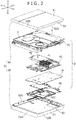
- FIG. 2 is an exploded perspective view of the electronic apparatus 1 depicted in FIG. 1 .
- FIG. 3 is a perspective view of a frame 20 and parts mounted to the frame 20, possessed by the electronic apparatus 1.
- FIG. 4 depicts perspective views depicting essential portions of the frame 20 and a lower chassis 30.
- FIG. 5 is a perspective view depicting an essential portion of a lower cover 50.
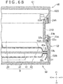
- FIG. 6A is a sectional view of the electronic apparatus 1 in a disassembled state, taken along line VI-VI of FIG. 1 .
- FIG. 6B is a sectional view depicting a state in which the parts depicted in FIG.
- FIG. 7 is a sectional view of the electronic apparatus in a disassembled state, taken along line VII-VIIB of FIG. 1 .
- FIG. 8A is a sectional view of the frame 20 and the covers 50 and 60 constituting the electronic apparatus, taken along line VIII-VIII of FIG. 1 .
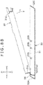
- FIG. 8B is a sectional view depicting the posture of the frame 20 in a process of combining the frame 20 and the lower cover 50 together.
- X1 and X2 depicted in FIG. 1 will respectively be a rightward direction and a leftward direction
- Y1 and Y2 will respectively be forward and rearward
- Z1 and Z2 will respectively be upward and downward.
- An electronic apparatus 1 is an entertainment device that functions as a game device or an audio/visual apparatus, for example.
- the electronic apparatus 1 outputs moving picture data produced by execution of a game program, video/audio data acquired from a recording medium such as an optical disk, and/or video/audio data acquired through a network, to a display device such as a television.
- the electronic apparatus 1 is not limited to the entertainment device such as a game device, but may be a personal computer.
- the electronic apparatus 1 has an inner part B and an armor member A that covers the inner part B.
- the armor member A includes a lower cover 50 that constitutes a lower surface of the electronic apparatus 1 and covers the lower side of the inner part B, and an upper cover 60 that constitutes an upper surface of the electronic apparatus 1 and covers the upper side of the inner part B.
- the upper cover 60, the lower cover 50 and the inner part B are combined together in the vertical direction.
- the upper cover 60, the lower cover 50 and a frame 20, which will be described later, are formed, for example, from a resin such as a plastic.
- the inner part B includes the frame 20, and various parts mounted to the frame 20, specifically a circuit board 10 and chassis 30 and 40.
- the electronic apparatus 1 has the upper chassis 40 covering the upper side of the circuit board 10, and the lower chassis 30 covering the lower side of the circuit board 10.
- the chassis 30 and 40 are formed from a metal, and have a function of securing rigidity of the frame 20, as well as a function of shielding electromagnetic waves generated from the circuit board 10 and shielding electromagnetic waves generated from external devices.
- a heat sink 41 for cooling an integrated circuit mounted on the circuit board may be mounted to the upper chassis 40.
- the upper chassis 40 may be provided with an accommodating section 42 for accommodating a hard disk device.
- the electronic apparatus 1 may not necessarily have the two chassis 30 and 40. In other words, the electronic apparatus 1 may have only either one of the chassis.
- the chassis 30 and 40 and the circuit board 10 are mounted to the lower side of the frame 20. More specifically, as depicted in FIG. 3 , the frame 20 has an outer peripheral section 21 configured by a front wall section 21A and a right wall section 21B and a rear wall section 21C and a left wall section 21D. The inside of the outer peripheral section 21 is open to the upper side and the lower side.
- the chassis 30 and 40 and the circuit board 10 are disposed on the lower side of the outer peripheral section 21, and are mounted to the outer peripheral section 21.
- the chassis 30 and 40 and the circuit board 10 are mounted to the outer peripheral section 21 by fixtures such as screws, for example.
- the lower chassis 30 has a guide section 31 (see FIG. 4 ) for facilitating assembly of the lower cover 50 and the inner part B and for increasing the degree of freedom in layout of parts.
- the guide section 31 will be described in detail later.
- the parts mounted to the frame 20 are not limited to these parts.
- an optical disk drive 7 for driving an optical disk a power supply unit 4 supplying driving electric power for the various parts possessed by the electronic apparatus 1, and the like may be mounted to the frame 20.
- These parts are disposed on the inside of the outer peripheral section 21, for example.
- a panel 6 covering the cooling fan 5 and the optical disk drive 7 is mounted to the frame 20.
- the lower cover 50 includes a lower panel section 51 located under the inner part B and covering the lower side of the inner part B, and a peripheral wall section 52 formed at an outer peripheral edge of the lower panel section 51.
- the peripheral wall section 52 extends upward from the outer peripheral edge of the lower panel section 51, and surrounds the outer periphery of the inner part B.
- the lower panel section 51 is substantially rectangular in shape, and the peripheral wall section 52 has four wall sections.
- the peripheral wall section 52 includes: a front wall section 52A formed at a front edge of the lower panel section 51 and located on the front side of the inner part B; a right wall section 52B formed at a right edge of the lower panel section 51 and located on the right side of the inner part B; a rear wall section 52C formed at a rear edge of the lower panel section 51 and located on the rear side of the inner part B; and a left wall section 52D forming at a left edge of the lower panel section 51 and located on the left side of the inner part B.
- the lower cover 50 is in the shape of a box opening to the upper side.
- the peripheral wall section 52 may not necessarily have the four wall sections.
- the peripheral wall section 52 may be configured by only three wall sections (for example, the front wall section 52A, the right wall section 52B, and the left wall section 52D).
- first engaging sections 53A (see FIG. 5 ) are formed at the right wall section 52B, as will be described in detail later.
- the first engaging sections 53A may be formed at any one of the wall sections.
- a second engaging section 53B (see FIG. 7 ) is formed at the left wall section 52D, as will be described in detail later.
- the second engaging section 53B may be formed at the wall section on the side opposite to the wall section at which the first engaging sections 53A are formed, and the position of the second engaging section 53B may be changed according to the wall section at which the first engaging sections 53A are formed.
- the upper cover 60 includes an upper panel section 61 located above the inner part B and covering the upper side of the inner part B, and a peripheral wall section 62 formed at an outer peripheral edge of the upper panel section 61.
- the peripheral wall section 62 extends downward from the outer peripheral edge of the upper panel section 61, and surrounds the outer periphery of the inner part B.
- the upper panel section 61 is substantially rectangular in shape, and the peripheral wall section 62 has four wall sections.
- the peripheral wall section 62 includes: a front wall section 62A formed at a front edge of the upper panel section 61 and located on the front side of the inner part B; a right wall section 62B formed at a right edge of the upper panel section 61 and located on the right side of the inner part B; a rear wall section 62C (see FIG. 8A ) formed at a rear edge of the upper panel section 61 and located on the rear side of the inner part B; and a left wall section 62D (see FIG. 7 ) formed at a left edge of the upper panel section 61 and located on the left side of the inner part B.
- the peripheral wall section 62 may not necessarily have the four wall sections.
- the peripheral wall section 62 may be configured by only three wall sections (the front wall section 62A, the right wall section 62B, and the left wall section 62D) .
- the right wall section 52B of the lower cover 50 has the first engaging sections 53A.
- the first engaging sections 53A are formed at an inner surface of the right wall section 52B, and project toward the inner side of the peripheral wall section 52 from the right wall section 52B.
- the inner part B has a first engaged section 23A.
- the first engaged section 23A is formed at an outer surface of the right wall section 21B of the frame 20, and projects toward the outer side (the right side) of the frame 20.
- the first engaged section 23A is located on the inner side of the peripheral wall section 52 in relation to the first engaging sections 53A in a state in which the inner part B and the lower cover 50 are combined together.
- an upper end of the right wall section 52B of the lower cover 50 is located above a lower end of the right wall section 21B of the frame 20. Therefore, an uppermost portion of the right wall section 52B and a lowermost portion of the right wall section 21B face each other.
- the first engaging sections 53A are formed at the uppermost portion of the right wall section 52B of the lower cover 50, and the first engaged section 23A is formed at the lowermost portion of the right wall section 21B of the frame 20.
- the first engaged section 23A is located on the inner side of the peripheral wall section 52 in relation to the first engaging sections 53A.
- the first engaged section 23A is engaged with the first engaging sections 53A.
- the inner part B has a first edge section S1 at an outer peripheral section thereof.
- the first edge section S1 is located below the first engaging sections 53A of the lower cover 50 in a state in which the inner part B and the lower cover 50 are combined together.
- the first edge section S1 is a part that overlaps with the first engaging sections 53A of the lower cover 50 when the inner part B and the lower cover 50 are viewed in the vertical direction.
- a part of an outer peripheral section of the inner part B overlaps with the first engaging sections 53A of the lower cover 50, and the overlapping part is the first edge section S1.
- the first edge section S1 is located between an outer surface of the frame 20 and an inner surface of the peripheral wall section 52 of the lower cover 50 when the inner part B and the lower cover 50 are viewed in the vertical direction.
- the circuit board 10 and the chassis 30 and 40 and the lower cover 50 are laid out in such a manner that outer peripheral sections of the circuit board 10 and the upper chassis 40 and the lower chassis 30 have the first edge section S1.
- the circuit board 10 and the chassis 30 and 40 are mounted to the frame 20 in such a manner that a part of their outer peripheral sections constitutes the first edge section S1.
- an end face 10b of the circuit board 10 is located on an outer side in relation to end surfaces (surfaces facing toward the inner side of the peripheral wall section 52) of the first engaging sections 53A of the lower cover 50 and an outer surface of the right wall section 21B of the frame 20.
- outer peripheral sections 30a and 40a of the chassis 30 and 40 extend to the end face 10b of the circuit board 10, and are in contact with a surface of the circuit board 10.
- the outer peripheral sections 30a and 40a of the chassis 30 and 40 may be electrically connected to a ground line provided at an outer peripheral section of the circuit board 10.
- the first edge section S1 is confirmed by only one or two of the three members consisting of the circuit board 10 and the chassis 30 and 40.
- the first edge section S1 may be composed of only an outer peripheral section of the circuit board 10, and the chassis 30 and 40 may not have a part constituting the first edge section S1.
- the first edge section S1 may be composed of only the outer peripheral section 30a or 40a of the upper chassis 40 or the lower chassis 30, and the circuit board 10 may not have a part constituting the first edge section S1.
- the first engaged section 23A projects outward (in the example of the electronic apparatus 1, rightward) from an outer surface of the right wall section 21B of the frame 20.
- the first engaged section 23A is located on the upper side of the first edge section S1. Besides, the first engaged section 23A overlaps with the first edge section S1 when the inner part B is viewed in the vertical direction.
- the first engaging sections 53A of the lower cover 50 and the first edge section S1 would collide on each other, in a process of combining the inner part B and the lower cover 50 together in the vertical direction, which would make the combining work troublesome.
- the inner part B is provided with a guide section 31.
- the guide section 31 is located below the first edge section S1.
- the first engaging sections 53A are located below the guide section 31. Therefore, in the process of combining the lower cover 50 and the inner part B together in the vertical direction, the first engaging sections 53A of the lower cover 50 come into contact with the guide section 31 earlier than the first edge section S1. Specifically, the guide section 31 comes into contact with the first engaging sections 53A located on the lower side of the guide section 31.
- the right wall section 52B of the cover 50 is pressed to the outer side thereof (rightward), and is elastically bent.
- the first engaging sections 53A are also moved to the outer side, and are moved beyond the first edge section S1 to the upper side of the first edge section S1.
- the first engaging sections 53A moved beyond the first edge section S1 are engaged with the first engaged section 23A.
- the guide section 31 prevents the first engaging sections 53A of the lower cover 50 and the first edge section S1 from colliding on each other in the process of combining the lower cover 50 and the inner part B together in the vertical direction. As a result, the work of combining the lower cover 50 and the inner part B together can be facilitated.
- the outer peripheral sections of the circuit board 10 and the chassis 30 and 40 can be disposed under the first engaging sections 53A, the degree of freedom in layout of them can be increased.
- the circuit board 10 and the chassis 30 and 40 can be disposed in extreme proximity to the right wall section 52B of the lower cover 50.
- the guide section 31 overlaps with the first engaging sections 53A of the lower cover 50 when the lower cover 50 and the inner part B are viewed in the vertical direction. Besides, the guide section 31 is formed such as to press the first engaging sections 53A, of the right wall section 52B of the lower cover 50.
- the guide section 31 has a slant surface 31a.
- the slant surface 31a is formed in such a manner that the right wall section 52b (more specifically, the first engaging sections 53A) having come into contact with the surface of the slant surface 31a is guided toward the outer side of the peripheral wall section 52.
- the slant surface 31a is inclined such as to extend toward the inner side and the lower side of the outer peripheral section 21 of the frame 20. In other words, the slant surface 31a approaches the end surface of the inner part B (the end face 10b of the circuit board 10) gradually in going from its lower edge toward its upper edge.
- the first engaging sections 53a first make contact with a position near the lower edge of the slant surface 31a, and then move toward the upper edge of the slant surface 31a.
- a guide section 31 in the process of combining the lower cover 50 and the inner part B together in the vertical direction, the first engaging sections 53A of the lower cover 50 come into contact with the guide section 31, and are pressed toward the outer side (the right side) of the peripheral wall section 53. Then, the first engaging sections 53A move beyond the first edge section S1 to the upper side of the first edge section S1.
- the lower chassis 30 is formed of a metallic sheet.
- the guide section 31 is formed in the lower chassis 30. Specifically, as depicted in FIG. 6A , an end portion of the lower chassis 30 is bent toward the side opposite to the first edge section S1, and the bent part constitutes the guide section 31. With a part of the lower chassis 30 thus utilized as the guide section 31, the guide section 31 can be formed comparatively easily, and an increase in the number of parts can be restrained.
- the guide section 31 is not limited to that in the example of the electronic apparatus 1.
- the guide section may be formed in the upper chassis 40.
- a right end portion of the upper chassis 40 may be bent toward the lower side, and may be disposed such as to be located on the lower side of a right end portion of the circuit board 10 (in other words, the first edge section S1).
- the guide section may be formed in other part possessed by the inner part B.
- the guide section may be configured by a part mounted on the circuit board 10.
- the right wall section 52B of the lower cover 50 has the plurality of first engaging sections 53A which are aligned in the front-rear direction (see FIG. 5 ).
- the guide section 31 also extends in the front-rear direction, and has a length corresponding to the positions of the plurality of first engaging sections 53A (see FIG. 4 ). According to such a guide section 31, it is easier to secure the strength of the guide section 31, as compared to the case where a plurality of guide sections 31 corresponding to the positions of the plurality of engaging sections 53 of the right wall section 52 are formed in the lower chassis 30.
- the guide section 31 may be partly cut between its front end and its rear end, as depicted in an example of FIG. 4 . In place of the example of FIG. 4 , the guide section 31 may be continuous from its front end to the rear end. In addition, a plurality of guide sections 31 corresponding to the positions of the plurality of first engaging sections 53 may be provided in the inner part B.
- the length of the guide section 31 is not particularly limited, so long as the guide section 31 is present on the lower side of one of the first engaging sections 53A.
- the first engaging sections 53A of the lower cover 50 are engaged with the first engaged section 23A in such a manner that the right wall section 52B is not separated from the first engaged section 23A toward the outer side (the right side) of the peripheral wall section 52.
- the first engaged section 23A is provided in the inner part B (more specifically, the frame 20), as aforementioned.
- the first engaging sections 53A of the lower cover 50 are engaged with the first engaged section 23A such that the right wall section 52B will not be separated from the frame 20 to the outer side (the right side).
- the first engaging sections 53A of the lower cover 50 have projections 53a projecting upward.
- the first engaged section 23A projects rightward from the right wall section 52B of the frame 20.
- the first engaged section 23A has a projection 23a projecting downward.
- the projections 53a of the first engaging sections 53A are engaged with the projection 23a of the first engaged section 23A.
- the projections 53a of the first engaging sections 53A are fitted between the projection 23a of the first engaged section 23A and an outer surface of the right wall section 21B of the frame 20, and the projection 23a of the first engaged section 23A is fitted between the projections 53a of the first engaging sections 53A and an inner surface of the right wall section 52B of the lower cover 50.
- the first engaged section 23A extends in the front-rear direction along the right wall section 21B of the frame 20.
- the length of the first engaged section 23A corresponds to the length of the right wall section 21B of the frame 20.
- the projection 23a extends in the front-rear direction, and a groove is formed between the projection 23a and an outer surface of the right wall section 21B.
- the shape of the first engaged section 23A is not restricted to that in the example of the electronic apparatus 1.
- the electronic apparatus 1 may have a plurality of first engaged sections 23A corresponding to the plurality of first engaging sections 53A.
- the first engaged section 23A is formed with holes 23b which penetrate the first engaged section 23A in the vertical direction.
- the holes 23b may function as ventilation holes for taking in external air into the electronic apparatus 1 therethrough.
- the first engaged section 23A may not be formed with the holes 23b for ventilation.
- the peripheral wall section 52 of the lower cover 50 has the left wall section 52D.
- the left wall section 52D has second engaging sections 53B projecting toward the inner side of the peripheral wall section 52, like the right wall section 52B.
- the inner part B has a second engaged section 23B.
- the second engaged section 23B is located on the inner side of the peripheral wall section 52 of the lower cover 50, and is engaged with the second engaging sections 53B.
- the second engaged section 23B is engaged with the second engaging sections 53B, to thereby restrict the left wall section 52D of the lower cover 50 from moving toward the outer side (the left side) of the peripheral wall section 52.
- the second engaged section 23B is formed in the left wall section 21D of the frame 20. Therefore, the second engaged section 23B restricts the left wall section 52D of the lower cover 50 from being separated leftward from the left wall section 21D of the frame 20.
- the second engaging sections 53B have the similar structure as the aforementioned first engaging sections 53A, and the second engaged section 23B has the similar structure as the aforementioned first engaged section 23A.
- the second engaging sections 53B of the lower cover 50 have projections 53a projecting upward.
- the second engaged section 23B projects leftward from the left wall section 52D of the frame 20.
- the second engaged section 23B has a projection 23a projecting downward.
- the projections 53a of the second engaging sections 53B are engaged with the projection 23a of the second engaged section 23B.
- the projections 53a of the second engaging sections 53B are fitted between the projection 23a of the second engaged section 23B and an outer surface of the left wall section 21D of the frame 20, and the projection 23a of the second engaged section 23B is fitted between the projections 53a of the second engaging sections 53B and an inner surface of the left wall section 52D of the lower cover 50.
- the first edge section S1 depicted in FIG. 6A and the like is not provided on the left side of the electronic apparatus 1. Therefore, in the process of combining the inner part B and the lower cover 50 together in the vertical direction, the second engaging sections 53B of the lower cover 50 are fitted to the second engaged section 23B without undergoing a process in which the left wall section 52D is pushed leftward.
- first edge section S1 may be provided also on the electronic apparatus, unlike in the example of the electronic apparatus 1.
- the front wall section 52A of the lower cover 50 has a projecting portion 54 projecting toward the inner side of the peripheral wall section 52, in other words, projecting toward the rear side.
- the projecting portion 54 is formed at an upper edge of the front wall section 52A.
- the projecting portion 54 extends in the left-right direction along the upper edge of the front wall section 52A.
- the projecting portion 54 extends from the left wall section 52D to the right wall section 52B of the lower cover 50.
- the inner part B has a second edge section S2 on the front side thereof.
- the second edge section S2 is located below the projecting portion 54 of the lower cover 50 in a state in which the inner part B and the lower cover 50 are combined together.
- the second edge section S2 is a part which is located beneath the projecting portion 54 of the lower cover 50 in the state in which the inner part B and the lower cover 50 are combined together and which overlaps with the projecting portion 54 of the lower cover 50 when the inner part B and the lower cover 50 are viewed in the vertical direction.
- a part of an outer peripheral section of the inner part B overlaps with the projecting portion 54 of the lower cover 50, and the overlapping part constitutes the second edge section S2.
- the inner part B and the lower cover 50 can be restrained from being separated from each other in the vertical direction. Specifically, the second edge section S2 is caught on the projecting portion 54 of the lower cover 50 in such a manner that the inner part B is not separated upward from the lower cover 50.
- the second edge section S2 is provided in the frame 20. Specifically, as depicted in FIG. 8A , a lower portion 21a of the front wall section 21A of the frame 20 protrudes forward. The lower portion 21a constitutes the second edge section S2.
- the lower portion 21 (the second edge section S2) of the front wall section 21A is formed to be along inner surfaces of the projecting portion 54 and the front wall section 52A of the lower cover 50. According to such a front wall section 21A, the parts possessed by the electronic apparatus 1 can be disposed in a space surrounded by the projecting portion 54 and the lower panel section 51 and the front wall section 52A, so that effective utilization of space can be achieved.
- the edge sections S1 and S2 are provided on the right side and the front side of the inner part B.
- the second edge section S2 is located in a direction intersecting the direction D1. More specifically, the second edge section S2 is located in the direction orthogonal to the direction D1. In other words, the first edge section S1 and the second edge section S2 are located at mutually intersecting two sides, of four sides of a rectangle.
- the electronic apparatus 1 having such edge sections S1 and S2 can be assembled, for example, in the following manner.
- the inner part B in FIG. 8B , only the frame 20 is depicted
- the second edge section S2 of the inner part B is fitted in between the projecting portion 54 and the lower panel section 51 of the lower cover 50.
- the rear side of the inner part B is lowered toward the lower cover 50.
- the first engaging sections 53A of the lower cover 50 come into contact with the guide section 31 of the inner part B (more specifically, the lower chassis 30). Consequently, the right wall section 52B of the lower cover 50 is bulged rightward.
- the first engaging sections 53A pass the outer side (the right side) of the first edge section S1 of the inner part B to move to the upper side of the first edge section S1 while being guided by the guide section 31, and are engaged with the first engaged section 23A.
- the second engaging sections 53B of the lower cover 50 are engaged with the second engaged section 23B of the inner part B, without coming into contact with the inner part B.
- the inner part B and the lower cover 50 are combined together.
- the lower cover 50 may be mounted to the inner part B by fixtures such as screws.
- the rear wall section 52C of the lower cover 50 may be mounted to the rear wall section 21C of the frame 20 by a fixture.
- the electronic apparatus 1 has the upper cover 60.
- the right wall section 62B of the upper cover 60 may also have an engaging section or sections 63A.
- the right wall section 21B of the frame 20 may have an engaged section 24A (see FIG. 4 ) for engagement with the engaging section or sections 63A.
- the left wall section 62D of the upper cover 60 may also have an engaging section or sections 63B (see FIG. 7 ).
- the left wall section 21D of the frame 20 may have an engaged section 24B for engagement with the engaging section or sections 63B.
- FIGS. 9 to 12 are figures for explaining the structure of a button member 70 possessed by the electronic apparatus 1.
- FIG. 9 is a perspective view of a portion where a button member 70 is disposed.
- FIG. 10 is a sectional view taken along line X-X of FIG. 9 .
- FIG. 11 is a perspective view of the button member 70.
- FIG. 12 is a perspective view of the lower cover 50 at which the button member 70 is disposed, as viewed from inside.
- the button member 70 is disposed at the lower cover 50.
- the lower cover 50 includes the lower panel section 51, the front wall section 52A formed at the front edge of the lower panel section 51, and the projecting portion 54 formed at the upper edge of the front wall section 52A and projecting to the rear side.
- the button member 70 is disposed on the lower side of the projecting portion 54. Specifically, the button member 70 is disposed in a space surrounded by the lower panel section 51 and the front wall section 52 and the projecting portion 54.
- the projecting portion 54 is formed with holes 54a and 54b (see FIG. 12 ), and top portions 70a and 70b (see FIG. 11 ) of the button member 70 are exposed through the holes 54a and 54b.
- the button member 70 includes a first button section 70A and a second button section 70B.
- the first button section 70A and the second button section 70B are formed integrally.
- the top portion 70a of the first button section 70A and the top portion 70b of the second button section 70B are exposed through the holes 54a and 54b, respectively.
- the first button section 70A and the second button section 70B are, for example, a power supply button for turning ON or OFF a power supply for the electronic apparatus 1 and an ejection button for ejecting an optical disk from the optical disk drive 7.
- a switch board (not depicted) on which switches are mounted is disposed on the lower side of the top portions 70a and 70b of the button sections 70A and 70B. When the button section 70A or 70B is depressed, the button section 70A or 70B turns a switch ON or OFF.
- the button member 70 has spring sections 71A and 71B.
- the spring sections 71A and 71B are disposed on the lower panel section 51, and bias the button sections 70A and 70B upward, or toward the projecting portion 54.
- the first button section 70A has a flange section 70c at a lower edge of the top portion 70a.
- the second button section 70B has a flange section 70d at a lower edge of the top portion 70b.
- the button sections 70A and 70B are being biased upward by the spring sections 71A and 71B, and the flange sections 70a and 70b are being pressed against the edges of the holes 54a and 54b, respectively.
- the spring sections 71A and 71B can be temporarily shrunk in a process of mounting the button member 70 to the lower cover 50, and, therefore, the work of mounting the button member 70 to the lower cover 50 can be facilitated.
- the button sections 70A and 70B are being biased upward by the spring sections 71A and 71B and being pressed against the edges of the holes 54a and 54b, the button sections 70A and 70B can be disposed at positions suitable for the holes 54a and 54b.
- the spring section 71A or 71B returns the button section 70A or 70B into an initial position. Therefore, the spring sections 70A and 70B of the button member 70 have two functions, namely, a function of facilitating the work of mounting the button member 70 and a function of returning the button sections 70A and 70B into initial positions.
- the two spring sections 71A and 71B have a connection section 71g at lower ends thereof.
- the connection section 71g has an extension section 71h extending rearward.
- a rear end of the extension section 71h is supported by, for example, a support portion formed in the lower panel section 51.
- the lower panel section 51 is formed with a recess 51f (see FIG. 12 ) in which to fit the rear end of the extension section 71h. According to such a structure, the posture of the button member 70 can be stabilized.
- the extension section 71h and the recess 51f may not necessarily be provided.
- the flange sections 70c and 70d of the button sections 70A and 70B have drooping sections 70e and 70f extending downward, on the front side thereof.
- One end (upper end) of the spring section 71A and one end (upper end) of the spring section 71B are connected to the drooping sections 70e and 70f, respectively.
- the other end (lower end) of the spring section 71A and the other end (lower end) of the spring section 71B are connected to each other.
- the spring sections 71A and 71B have curved sections 70m and 70n which are curved such as to bulge to opposite sides.
- the spring section 71A or 71B When the button section 70A or 70B is depressed, the spring section 71A or 71B exhibits an elastic force by flexure of the curved section 70m or 70n. As depicted in FIG. 12 , the lower panel section 51 is formed with ribs 51a and 51b projecting upward. The spring sections 71A and 71B are located respectively over the ribs 51a and 51b, and are supported by the ribs 51a and 51b when the button sections 70A and 70B are depressed.
- the front wall section 52A of the lower cover 50 has a rib 52f formed along an inner surface thereof.
- the rib 52f is located between the two button sections 70A and 70B. The posture of the two button sections 70A and 70B can be stabilized by the rib 52f.
- the lower cover 50 has the first engaging sections 53A, and the inner part B has the first edge section S1.
- the inner part B has the guide section 31 located below the first edge section S1.
- the guide section 31 is formed in such a manner that in the process of combining the lower cover 50 and the inner part B together in the vertical direction, it comes into contact with the right wall section 52B of the lower cover 50 to push the right wall section 52B rightward, and the first engaging sections 53A move beyond the first edge section S1 to the upper side of the first edge section S1.
- the electronic apparatus 1 has had the frame 20, and the circuit board 10 and the chassis 30 and 40 have been mounted to the frame 20.
- the electronic apparatus 1 may not necessarily have the frame 20.
- the electronic apparatus 1 may have an upper housing and a lower housing which are combined with each other in the vertical direction to form a box.
- the circuit board 10 and the chassis 30 and 40 may be fixed to the lower housing.
- the circuit board 10 and the chassis 30 and 40 may have the first edge section S1
- the upper housing may be formed with the first engaging sections
- the lower housing may be formed with the first engaged section.
- the upper chassis 40 may be formed with a guide section for pressing the first engaging sections of the upper housing to the outer side.
- the outer peripheral sections of the circuit board 10 and the chassis 30 and 40 have constituted the first edge section S1.
- the first edge section S1 may be configured by other part. Specifically, a part of the other part may be disposed such as to overlap with the first engaging sections 53A of the lower cover 50 in the vertical direction.
Landscapes
- Engineering & Computer Science (AREA)
- Microelectronics & Electronic Packaging (AREA)
- Computer Hardware Design (AREA)
- Physics & Mathematics (AREA)
- General Engineering & Computer Science (AREA)
- Theoretical Computer Science (AREA)
- Thermal Sciences (AREA)
- Human Computer Interaction (AREA)
- General Physics & Mathematics (AREA)
- Casings For Electric Apparatus (AREA)
- Mounting Of Printed Circuit Boards And The Like (AREA)
Abstract
Description
- The present invention relates to a vent hole of an electronic apparatus.
- An electronic apparatus of
PTL 1 set forth below includes a frame, an upper cover that covers the upper side of the frame, and a lower cover that covers the lower side of the frame. The frame has an outer peripheral section that surrounds various parts such as a cooling fan, a power supply unit, and an optical disk drive. These parts are mounted to the frame. - The upper cover has a peripheral wall section that surrounds the outer peripheral section of the frame. The upper cover is formed at an inner surface of the peripheral wall section thereof with engaging section projecting to the inner side, and the frame is formed with engaged sections at an outer surface of the outer peripheral section thereof. The engaging sections of the upper cover are caught on the engaged sections of the frame. By this, the peripheral wall section of the upper cover is restrained from being separated from the frame when a force of pulling the peripheral wall section of the upper cover to the outer side (a force for separating the peripheral wall section of the upper cover from the outer peripheral section of the frame) is exerted. The lower cover also has a peripheral wall section that surrounds the outer peripheral section of the frame. The lower cover also is formed with the similar structure as that of the upper cover. Specifically, the lower cover is formed at an inner surface of the peripheral wall section thereof with engaging sections projecting to the inner side. The engaging sections of the lower cover are caught on engaged sections formed in the frame.
-
- In the structure of the electronic apparatus disclosed in
PTL 1, if a portion of the parts mounted to the frame is protruding to the outside of an outer peripheral edge of the frame (in other words, if a portion of the parts mounted to the frame is located immediately over or beneath the engaging section of the cover), the engaging section of the cover would come into contact with the protruding parts, in a process of combining the frame and the cover together in the vertical direction, so that it would be impossible to smoothly perform the assembling work. Therefore, the parts mounted to the frame should be laid out in such a manner as not to have any portion protruding to the outside from the outer peripheral edge of the frame. - An electronic apparatus for solving the above-mentioned problem includes an inner part, and an armor member disposed on one side in a first direction in relation to the inner part and covering the inner part. The inner part includes a first edge section and a guide section located on the one side in the first direction in relation to the first edge section. The armor member includes a peripheral wall section which includes in part thereof a first wall section located in a second direction intersecting the first direction in relation to the inner part and which surrounds an outer periphery of the inner part, and a first engaging section which is formed in the first wall section and which projects toward an inner side of the peripheral wall section. The first engaging section of the armor member is located on the other side in the first direction in relation to the first edge section of the inner part, in a state in which the inner part and the armor member are combined together in the first direction, and is disposed at such a position as to overlap with the first edge section of the inner part when the armor member and the inner part are viewed in the first direction, and is engaged with a first engaged section located on the inner side of the peripheral wall section. The guide section of the inner part is formed in such a manner that in a process in which the inner part and the armor member are combined together in the first direction, the guide section comes into contact with the first wall section located on the one side in the first direction in relation to the guide section to push the first wall section in the second direction, so as to cause the first engaging section to go over the first edge section of the inner part to reach the other side in the first direction.
- According to this electronic apparatus, it is possible to increase the degree of freedom in layout of parts.
-
- [
FIG. 1 ]
FIG. 1 is a perspective view of an electronic apparatus according to an embodiment of the present invention. - [
FIG. 2 ]
FIG. 2 is an exploded perspective view of the electronic apparatus depicted inFIG. 1 . - [
FIG. 3 ]
FIG. 3 is a perspective view of a frame and parts mounted to the frame, possessed by the electronic apparatus. - [
FIG. 4 ]
FIG. 4 depicts perspective views depicting essential portions of the frame and a lower chassis, possessed by the electronic apparatus. - [
FIG. 5 ]
FIG. 5 is a perspective view depicting an essential portion of a lower cover possessed by the electronic apparatus. - [
FIG. 6A ]
FIG. 6A is a sectional view of the electronic apparatus in a disassembled state, taken along line VI-VI ofFIG. 1 . - [
FIG. 6B ]
FIG. 6B is a sectional view depicting a state in which the parts depicted inFIG. 6A are combined together. - [
FIG. 7 ]
FIG. 7 is a sectional view of the electronic apparatus in a disassembled state, taken along line VII-VIIB ofFIG. 1 . - [
FIG. 8A ]
FIG. 8A is a sectional view of the electronic apparatus in a disassembled state, taken along line VIII-VIII ofFIG. 1 . - [
FIG. 8B ]
FIG. 8B is a sectional view depicting the posture of the frame in a process of uniting the frame and the lower cover, possessed by the electronic apparatus. - [
FIG. 9 ]
FIG. 9 is a perspective view of a portion where a button member is disposed. - [
FIG. 10 ]
FIG. 10 is a sectional view taken along line X-X ofFIG. 9 . - [
FIG. 11 ]
FIG. 11 is a perspective view of the button member. - [
FIG. 12 ]
FIG. 12 is a perspective view of the lower cover at which the button member is disposed, as viewed from inside. - An embodiment of the present invention will be described below, referring to the drawings.
FIG. 1 is a perspective view of anelectronic apparatus 1 according to an embodiment of the present invention.FIG. 2 is an exploded perspective view of theelectronic apparatus 1 depicted inFIG. 1 .FIG. 3 is a perspective view of aframe 20 and parts mounted to theframe 20, possessed by theelectronic apparatus 1.FIG. 4 depicts perspective views depicting essential portions of theframe 20 and alower chassis 30.FIG. 5 is a perspective view depicting an essential portion of alower cover 50.FIG. 6A is a sectional view of theelectronic apparatus 1 in a disassembled state, taken along line VI-VI ofFIG. 1 .FIG. 6B is a sectional view depicting a state in which the parts depicted inFIG. 6A are combined together.FIG. 7 is a sectional view of the electronic apparatus in a disassembled state, taken along line VII-VIIB ofFIG. 1 .FIG. 8A is a sectional view of theframe 20 and thecovers FIG. 1 .FIG. 8B is a sectional view depicting the posture of theframe 20 in a process of combining theframe 20 and thelower cover 50 together. - In the following description, X1 and X2 depicted in
FIG. 1 will respectively be a rightward direction and a leftward direction, Y1 and Y2 will respectively be forward and rearward, and Z1 and Z2 will respectively be upward and downward. - An
electronic apparatus 1 is an entertainment device that functions as a game device or an audio/visual apparatus, for example. Theelectronic apparatus 1 outputs moving picture data produced by execution of a game program, video/audio data acquired from a recording medium such as an optical disk, and/or video/audio data acquired through a network, to a display device such as a television. Theelectronic apparatus 1 is not limited to the entertainment device such as a game device, but may be a personal computer. - As depicted in
FIG. 2 , theelectronic apparatus 1 has an inner part B and an armor member A that covers the inner part B. In the example of theelectronic apparatus 1, the armor member A includes alower cover 50 that constitutes a lower surface of theelectronic apparatus 1 and covers the lower side of the inner part B, and anupper cover 60 that constitutes an upper surface of theelectronic apparatus 1 and covers the upper side of the inner part B. As will be described later, theupper cover 60, thelower cover 50 and the inner part B are combined together in the vertical direction. Theupper cover 60, thelower cover 50 and aframe 20, which will be described later, are formed, for example, from a resin such as a plastic. - In addition, in the example of the
electronic apparatus 1, as depicted inFIG. 2 , the inner part B includes theframe 20, and various parts mounted to theframe 20, specifically acircuit board 10 andchassis electronic apparatus 1 has theupper chassis 40 covering the upper side of thecircuit board 10, and thelower chassis 30 covering the lower side of thecircuit board 10. Thechassis frame 20, as well as a function of shielding electromagnetic waves generated from thecircuit board 10 and shielding electromagnetic waves generated from external devices. - As depicted in
FIG. 3 , aheat sink 41 for cooling an integrated circuit mounted on the circuit board may be mounted to theupper chassis 40. In addition, theupper chassis 40 may be provided with anaccommodating section 42 for accommodating a hard disk device. Besides, theelectronic apparatus 1 may not necessarily have the twochassis electronic apparatus 1 may have only either one of the chassis. - In the example of the
electronic apparatus 1, thechassis circuit board 10 are mounted to the lower side of theframe 20. More specifically, as depicted inFIG. 3 , theframe 20 has an outerperipheral section 21 configured by afront wall section 21A and aright wall section 21B and arear wall section 21C and aleft wall section 21D. The inside of the outerperipheral section 21 is open to the upper side and the lower side. Thechassis circuit board 10 are disposed on the lower side of the outerperipheral section 21, and are mounted to the outerperipheral section 21. Thechassis circuit board 10 are mounted to the outerperipheral section 21 by fixtures such as screws, for example. In the example of theelectronic apparatus 1, thelower chassis 30 has a guide section 31 (seeFIG. 4 ) for facilitating assembly of thelower cover 50 and the inner part B and for increasing the degree of freedom in layout of parts. Theguide section 31 will be described in detail later. - The parts mounted to the
frame 20 are not limited to these parts. For example, as depicted inFIG. 3 , a coolingfan 5 for cooling the integrated circuit mounted on thecircuit board 10, anoptical disk drive 7 for driving an optical disk, apower supply unit 4 supplying driving electric power for the various parts possessed by theelectronic apparatus 1, and the like may be mounted to theframe 20. These parts are disposed on the inside of the outerperipheral section 21, for example. In the example of theelectronic apparatus 1, apanel 6 covering the coolingfan 5 and theoptical disk drive 7 is mounted to theframe 20. - As depicted in
FIG. 2 , thelower cover 50 includes alower panel section 51 located under the inner part B and covering the lower side of the inner part B, and aperipheral wall section 52 formed at an outer peripheral edge of thelower panel section 51. Theperipheral wall section 52 extends upward from the outer peripheral edge of thelower panel section 51, and surrounds the outer periphery of the inner part B. In the example of theelectronic apparatus 1, thelower panel section 51 is substantially rectangular in shape, and theperipheral wall section 52 has four wall sections. Specifically, theperipheral wall section 52 includes: afront wall section 52A formed at a front edge of thelower panel section 51 and located on the front side of the inner part B; aright wall section 52B formed at a right edge of thelower panel section 51 and located on the right side of the inner part B; arear wall section 52C formed at a rear edge of thelower panel section 51 and located on the rear side of the inner part B; and aleft wall section 52D forming at a left edge of thelower panel section 51 and located on the left side of the inner part B. In other words, in the example of theelectronic apparatus 1, thelower cover 50 is in the shape of a box opening to the upper side. Theperipheral wall section 52 may not necessarily have the four wall sections. For example, theperipheral wall section 52 may be configured by only three wall sections (for example, thefront wall section 52A, theright wall section 52B, and theleft wall section 52D). In theelectronic apparatus 1, first engagingsections 53A (seeFIG. 5 ) are formed at theright wall section 52B, as will be described in detail later. However, the first engagingsections 53A may be formed at any one of the wall sections. In addition, in theelectronic apparatus 1, a secondengaging section 53B (seeFIG. 7 ) is formed at theleft wall section 52D, as will be described in detail later. However, the second engagingsection 53B may be formed at the wall section on the side opposite to the wall section at which the first engagingsections 53A are formed, and the position of the second engagingsection 53B may be changed according to the wall section at which the first engagingsections 53A are formed. - As depicted in
FIG. 2 , theupper cover 60 includes anupper panel section 61 located above the inner part B and covering the upper side of the inner part B, and aperipheral wall section 62 formed at an outer peripheral edge of theupper panel section 61. Theperipheral wall section 62 extends downward from the outer peripheral edge of theupper panel section 61, and surrounds the outer periphery of the inner part B. In the example of theelectronic apparatus 1, theupper panel section 61 is substantially rectangular in shape, and theperipheral wall section 62 has four wall sections. Specifically, theperipheral wall section 62 includes: afront wall section 62A formed at a front edge of theupper panel section 61 and located on the front side of the inner part B; aright wall section 62B formed at a right edge of theupper panel section 61 and located on the right side of the inner part B; arear wall section 62C (seeFIG. 8A ) formed at a rear edge of theupper panel section 61 and located on the rear side of the inner part B; and aleft wall section 62D (seeFIG. 7 ) formed at a left edge of theupper panel section 61 and located on the left side of the inner part B. Theperipheral wall section 62 may not necessarily have the four wall sections. For example, theperipheral wall section 62 may be configured by only three wall sections (thefront wall section 62A, theright wall section 62B, and theleft wall section 62D) . - As depicted in
FIG. 6A , theright wall section 52B of thelower cover 50 has the first engagingsections 53A. The firstengaging sections 53A are formed at an inner surface of theright wall section 52B, and project toward the inner side of theperipheral wall section 52 from theright wall section 52B. On the other hand, the inner part B has a firstengaged section 23A. In the example of theelectronic apparatus 1, the firstengaged section 23A is formed at an outer surface of theright wall section 21B of theframe 20, and projects toward the outer side (the right side) of theframe 20. - As depicted in
FIG. 6B , the firstengaged section 23A is located on the inner side of theperipheral wall section 52 in relation to the first engagingsections 53A in a state in which the inner part B and thelower cover 50 are combined together. In the example of theelectronic apparatus 1, in the state in which the inner part B and thelower cover 50 are combined together, an upper end of theright wall section 52B of thelower cover 50 is located above a lower end of theright wall section 21B of theframe 20. Therefore, an uppermost portion of theright wall section 52B and a lowermost portion of theright wall section 21B face each other. The firstengaging sections 53A are formed at the uppermost portion of theright wall section 52B of thelower cover 50, and the firstengaged section 23A is formed at the lowermost portion of theright wall section 21B of theframe 20. As a result, the firstengaged section 23A is located on the inner side of theperipheral wall section 52 in relation to the first engagingsections 53A. Besides, in the state in which the inner part B and thelower cover 50 are combined together, the firstengaged section 23A is engaged with the first engagingsections 53A. By the engagement between the firstengaged section 23A and the first engagingsections 53A, a rightward relative movement of theright wall section 52B of thelower cover 50, or a deformation such as bulging of theright wall section 52B toward the outer side of theperipheral wall section 52, is restrained. - As depicted in
FIG. 6B , the inner part B has a first edge section S1 at an outer peripheral section thereof. The first edge section S1 is located below the first engagingsections 53A of thelower cover 50 in a state in which the inner part B and thelower cover 50 are combined together. The first edge section S1 is a part that overlaps with the first engagingsections 53A of thelower cover 50 when the inner part B and thelower cover 50 are viewed in the vertical direction. Specifically, a part of an outer peripheral section of the inner part B overlaps with the first engagingsections 53A of thelower cover 50, and the overlapping part is the first edge section S1. The first edge section S1 is located between an outer surface of theframe 20 and an inner surface of theperipheral wall section 52 of thelower cover 50 when the inner part B and thelower cover 50 are viewed in the vertical direction. - In the example of the
electronic apparatus 1, thecircuit board 10 and thechassis lower cover 50 are laid out in such a manner that outer peripheral sections of thecircuit board 10 and theupper chassis 40 and thelower chassis 30 have the first edge section S1. In other words, thecircuit board 10 and thechassis frame 20 in such a manner that a part of their outer peripheral sections constitutes the first edge section S1. In the example of theelectronic apparatus 1, anend face 10b of thecircuit board 10 is located on an outer side in relation to end surfaces (surfaces facing toward the inner side of the peripheral wall section 52) of the first engagingsections 53A of thelower cover 50 and an outer surface of theright wall section 21B of theframe 20. - As depicted in
FIG. 6A , outerperipheral sections chassis end face 10b of thecircuit board 10, and are in contact with a surface of thecircuit board 10. The outerperipheral sections chassis circuit board 10. - Note that a configuration may be adopted in which, unlike in the example of the
electronic apparatus 1, the first edge section S1 is confirmed by only one or two of the three members consisting of thecircuit board 10 and thechassis circuit board 10, and thechassis peripheral section upper chassis 40 or thelower chassis 30, and thecircuit board 10 may not have a part constituting the first edge section S1. - As depicted in
FIG. 6A , the firstengaged section 23A projects outward (in the example of theelectronic apparatus 1, rightward) from an outer surface of theright wall section 21B of theframe 20. The firstengaged section 23A is located on the upper side of the first edge section S1. Besides, the firstengaged section 23A overlaps with the first edge section S1 when the inner part B is viewed in the vertical direction. - According to the structure in which the inner part B has the first edge section S1, the first engaging
sections 53A of thelower cover 50 and the first edge section S1 would collide on each other, in a process of combining the inner part B and thelower cover 50 together in the vertical direction, which would make the combining work troublesome. - In view of this, in the example of the
electronic apparatus 1, as depicted inFIG. 6A , the inner part B is provided with aguide section 31. Theguide section 31 is located below the first edge section S1. In a state before thelower cover 50 and the inner part B are combined together, the first engagingsections 53A are located below theguide section 31. Therefore, in the process of combining thelower cover 50 and the inner part B together in the vertical direction, the first engagingsections 53A of thelower cover 50 come into contact with theguide section 31 earlier than the first edge section S1. Specifically, theguide section 31 comes into contact with the first engagingsections 53A located on the lower side of theguide section 31. As a result, theright wall section 52B of thecover 50 is pressed to the outer side thereof (rightward), and is elastically bent. In this instance, the first engagingsections 53A are also moved to the outer side, and are moved beyond the first edge section S1 to the upper side of the first edge section S1. As depicted inFIG. 6B , the first engagingsections 53A moved beyond the first edge section S1 are engaged with the firstengaged section 23A. In this way, theguide section 31 prevents the first engagingsections 53A of thelower cover 50 and the first edge section S1 from colliding on each other in the process of combining thelower cover 50 and the inner part B together in the vertical direction. As a result, the work of combining thelower cover 50 and the inner part B together can be facilitated. In addition, since the outer peripheral sections of thecircuit board 10 and thechassis sections 53A, the degree of freedom in layout of them can be increased. In other words, thecircuit board 10 and thechassis right wall section 52B of thelower cover 50. - In the example of the
electronic apparatus 1, theguide section 31 overlaps with the first engagingsections 53A of thelower cover 50 when thelower cover 50 and the inner part B are viewed in the vertical direction. Besides, theguide section 31 is formed such as to press the first engagingsections 53A, of theright wall section 52B of thelower cover 50. - As depicted in
FIG. 6A , theguide section 31 has aslant surface 31a. Theslant surface 31a is formed in such a manner that the right wall section 52b (more specifically, the first engagingsections 53A) having come into contact with the surface of theslant surface 31a is guided toward the outer side of theperipheral wall section 52. Specifically, theslant surface 31a is inclined such as to extend toward the inner side and the lower side of the outerperipheral section 21 of theframe 20. In other words, theslant surface 31a approaches the end surface of the inner part B (theend face 10b of the circuit board 10) gradually in going from its lower edge toward its upper edge. The firstengaging sections 53a first make contact with a position near the lower edge of theslant surface 31a, and then move toward the upper edge of theslant surface 31a. According to such aguide section 31, in the process of combining thelower cover 50 and the inner part B together in the vertical direction, the first engagingsections 53A of thelower cover 50 come into contact with theguide section 31, and are pressed toward the outer side (the right side) of the peripheral wall section 53. Then, the first engagingsections 53A move beyond the first edge section S1 to the upper side of the first edge section S1. - As aforementioned, the
lower chassis 30 is formed of a metallic sheet. In the example of theelectronic apparatus 1, theguide section 31 is formed in thelower chassis 30. Specifically, as depicted inFIG. 6A , an end portion of thelower chassis 30 is bent toward the side opposite to the first edge section S1, and the bent part constitutes theguide section 31. With a part of thelower chassis 30 thus utilized as theguide section 31, theguide section 31 can be formed comparatively easily, and an increase in the number of parts can be restrained. - The
guide section 31 is not limited to that in the example of theelectronic apparatus 1. For example, the guide section may be formed in theupper chassis 40. In this case, a right end portion of theupper chassis 40 may be bent toward the lower side, and may be disposed such as to be located on the lower side of a right end portion of the circuit board 10 (in other words, the first edge section S1). In addition, the guide section may be formed in other part possessed by the inner part B. For example, the guide section may be configured by a part mounted on thecircuit board 10. - In the example of the
electronic apparatus 1, theright wall section 52B of thelower cover 50 has the plurality of firstengaging sections 53A which are aligned in the front-rear direction (seeFIG. 5 ). Theguide section 31 also extends in the front-rear direction, and has a length corresponding to the positions of the plurality of firstengaging sections 53A (seeFIG. 4 ). According to such aguide section 31, it is easier to secure the strength of theguide section 31, as compared to the case where a plurality ofguide sections 31 corresponding to the positions of the plurality of engaging sections 53 of theright wall section 52 are formed in thelower chassis 30. - The
guide section 31 may be partly cut between its front end and its rear end, as depicted in an example ofFIG. 4 . In place of the example ofFIG. 4 , theguide section 31 may be continuous from its front end to the rear end. In addition, a plurality ofguide sections 31 corresponding to the positions of the plurality of first engaging sections 53 may be provided in the inner part B. The length of theguide section 31 is not particularly limited, so long as theguide section 31 is present on the lower side of one of the first engagingsections 53A. - The first
engaging sections 53A of thelower cover 50 are engaged with the firstengaged section 23A in such a manner that theright wall section 52B is not separated from the firstengaged section 23A toward the outer side (the right side) of theperipheral wall section 52. In the example of theelectronic apparatus 1, the firstengaged section 23A is provided in the inner part B (more specifically, the frame 20), as aforementioned. The firstengaging sections 53A of thelower cover 50 are engaged with the firstengaged section 23A such that theright wall section 52B will not be separated from theframe 20 to the outer side (the right side). - In the example of the
electronic apparatus 1, as depicted inFIG. 6A , the first engagingsections 53A of thelower cover 50 haveprojections 53a projecting upward. The firstengaged section 23A projects rightward from theright wall section 52B of theframe 20. Besides, the firstengaged section 23A has aprojection 23a projecting downward. As depicted inFIG. 6B , theprojections 53a of the first engagingsections 53A are engaged with theprojection 23a of the firstengaged section 23A. Specifically, theprojections 53a of the first engagingsections 53A are fitted between theprojection 23a of the firstengaged section 23A and an outer surface of theright wall section 21B of theframe 20, and theprojection 23a of the firstengaged section 23A is fitted between theprojections 53a of the first engagingsections 53A and an inner surface of theright wall section 52B of thelower cover 50. - In the example of the
electronic apparatus 1, as depicted inFIG. 4 , the firstengaged section 23A extends in the front-rear direction along theright wall section 21B of theframe 20. The length of the firstengaged section 23A corresponds to the length of theright wall section 21B of theframe 20. Theprojection 23a extends in the front-rear direction, and a groove is formed between theprojection 23a and an outer surface of theright wall section 21B. The shape of the firstengaged section 23A is not restricted to that in the example of theelectronic apparatus 1. For example, theelectronic apparatus 1 may have a plurality of firstengaged sections 23A corresponding to the plurality of firstengaging sections 53A. - As depicted in
FIG. 4 , in the example of theelectronic apparatus 1, the firstengaged section 23A is formed withholes 23b which penetrate the firstengaged section 23A in the vertical direction. Theholes 23b may function as ventilation holes for taking in external air into theelectronic apparatus 1 therethrough. The firstengaged section 23A may not be formed with theholes 23b for ventilation. - As aforementioned, the
peripheral wall section 52 of thelower cover 50 has theleft wall section 52D. As depicted inFIG. 7 , theleft wall section 52D has second engagingsections 53B projecting toward the inner side of theperipheral wall section 52, like theright wall section 52B. The inner part B has a secondengaged section 23B. The secondengaged section 23B is located on the inner side of theperipheral wall section 52 of thelower cover 50, and is engaged with the secondengaging sections 53B. The secondengaged section 23B is engaged with the secondengaging sections 53B, to thereby restrict theleft wall section 52D of thelower cover 50 from moving toward the outer side (the left side) of theperipheral wall section 52. In the example of theelectronic apparatus 1, the secondengaged section 23B is formed in theleft wall section 21D of theframe 20. Therefore, the secondengaged section 23B restricts theleft wall section 52D of thelower cover 50 from being separated leftward from theleft wall section 21D of theframe 20. - The second
engaging sections 53B have the similar structure as the aforementioned first engagingsections 53A, and the secondengaged section 23B has the similar structure as the aforementioned firstengaged section 23A. Specifically, in the example of theelectronic apparatus 1, the secondengaging sections 53B of thelower cover 50 haveprojections 53a projecting upward. The secondengaged section 23B projects leftward from theleft wall section 52D of theframe 20. The secondengaged section 23B has aprojection 23a projecting downward. Theprojections 53a of the secondengaging sections 53B are engaged with theprojection 23a of the secondengaged section 23B. Specifically, theprojections 53a of the secondengaging sections 53B are fitted between theprojection 23a of the secondengaged section 23B and an outer surface of theleft wall section 21D of theframe 20, and theprojection 23a of the secondengaged section 23B is fitted between theprojections 53a of the secondengaging sections 53B and an inner surface of theleft wall section 52D of thelower cover 50. - In one example, the first edge section S1 depicted in
FIG. 6A and the like is not provided on the left side of theelectronic apparatus 1. Therefore, in the process of combining the inner part B and thelower cover 50 together in the vertical direction, the secondengaging sections 53B of thelower cover 50 are fitted to the secondengaged section 23B without undergoing a process in which theleft wall section 52D is pushed leftward. - Note that the first edge section S1 may be provided also on the electronic apparatus, unlike in the example of the
electronic apparatus 1. In this case, it is desirable for thelower chassis 30 to have theguide section 31 also at a left edge portion thereof. - As depicted in
FIGS. 5 and8A , thefront wall section 52A of thelower cover 50 has a projectingportion 54 projecting toward the inner side of theperipheral wall section 52, in other words, projecting toward the rear side. In the example of theelectronic apparatus 1, the projectingportion 54 is formed at an upper edge of thefront wall section 52A. The projectingportion 54 extends in the left-right direction along the upper edge of thefront wall section 52A. In the example of theelectronic apparatus 1, the projectingportion 54 extends from theleft wall section 52D to theright wall section 52B of thelower cover 50. - As depicted in
FIGS. 3 and8A , the inner part B has a second edge section S2 on the front side thereof. The second edge section S2 is located below the projectingportion 54 of thelower cover 50 in a state in which the inner part B and thelower cover 50 are combined together. The second edge section S2 is a part which is located beneath the projectingportion 54 of thelower cover 50 in the state in which the inner part B and thelower cover 50 are combined together and which overlaps with the projectingportion 54 of thelower cover 50 when the inner part B and thelower cover 50 are viewed in the vertical direction. Specifically, a part of an outer peripheral section of the inner part B overlaps with the projectingportion 54 of thelower cover 50, and the overlapping part constitutes the second edge section S2. By such a second edge section S2, the inner part B and thelower cover 50 can be restrained from being separated from each other in the vertical direction. Specifically, the second edge section S2 is caught on the projectingportion 54 of thelower cover 50 in such a manner that the inner part B is not separated upward from thelower cover 50. - In the example of the
electronic apparatus 1, the second edge section S2 is provided in theframe 20. Specifically, as depicted inFIG. 8A , alower portion 21a of thefront wall section 21A of theframe 20 protrudes forward. Thelower portion 21a constitutes the second edge section S2. In the example of theelectronic apparatus 1, the lower portion 21 (the second edge section S2) of thefront wall section 21A is formed to be along inner surfaces of the projectingportion 54 and thefront wall section 52A of thelower cover 50. According to such afront wall section 21A, the parts possessed by theelectronic apparatus 1 can be disposed in a space surrounded by the projectingportion 54 and thelower panel section 51 and thefront wall section 52A, so that effective utilization of space can be achieved. - In this way, in the example of the
electronic apparatus 1, the edge sections S1 and S2 are provided on the right side and the front side of the inner part B. Specifically, when the direction where the first edge section S1 is located relative to the inner part B is defined as the direction D1, the second edge section S2 is located in a direction intersecting the direction D1. More specifically, the second edge section S2 is located in the direction orthogonal to the direction D1. In other words, the first edge section S1 and the second edge section S2 are located at mutually intersecting two sides, of four sides of a rectangle. - The
electronic apparatus 1 having such edge sections S1 and S2 can be assembled, for example, in the following manner. As depicted inFIG. 8B , first, the inner part B (inFIG. 8B , only theframe 20 is depicted) is inclined relative to thelower cover 50, and the second edge section S2 of the inner part B is fitted in between the projectingportion 54 and thelower panel section 51 of thelower cover 50. Thereafter, as indicated by arrow H inFIG. 8B , the rear side of the inner part B is lowered toward thelower cover 50. In this instance, the first engagingsections 53A of thelower cover 50 come into contact with theguide section 31 of the inner part B (more specifically, the lower chassis 30). Consequently, theright wall section 52B of thelower cover 50 is bulged rightward. Then, the first engagingsections 53A pass the outer side (the right side) of the first edge section S1 of the inner part B to move to the upper side of the first edge section S1 while being guided by theguide section 31, and are engaged with the firstengaged section 23A. On the other hand, the secondengaging sections 53B of thelower cover 50 are engaged with the secondengaged section 23B of the inner part B, without coming into contact with the inner part B. By such a procedure, the inner part B and thelower cover 50 are combined together. Note that thelower cover 50 may be mounted to the inner part B by fixtures such as screws. For example, therear wall section 52C of thelower cover 50 may be mounted to therear wall section 21C of theframe 20 by a fixture. - As aforementioned, the
electronic apparatus 1 has theupper cover 60. As depicted inFIG. 6A , theright wall section 62B of theupper cover 60 may also have an engaging section orsections 63A. In addition, theright wall section 21B of theframe 20 may have an engagedsection 24A (seeFIG. 4 ) for engagement with the engaging section orsections 63A. Similarly, theleft wall section 62D of theupper cover 60 may also have an engaging section orsections 63B (seeFIG. 7 ). Besides, theleft wall section 21D of theframe 20 may have an engagedsection 24B for engagement with the engaging section orsections 63B. -
FIGS. 9 to 12 are figures for explaining the structure of abutton member 70 possessed by theelectronic apparatus 1.FIG. 9 is a perspective view of a portion where abutton member 70 is disposed.FIG. 10 is a sectional view taken along line X-X ofFIG. 9 .FIG. 11 is a perspective view of thebutton member 70.FIG. 12 is a perspective view of thelower cover 50 at which thebutton member 70 is disposed, as viewed from inside. - As depicted in
FIG. 9 , in the example of theelectronic apparatus 1, thebutton member 70 is disposed at thelower cover 50. As aforementioned, thelower cover 50 includes thelower panel section 51, thefront wall section 52A formed at the front edge of thelower panel section 51, and the projectingportion 54 formed at the upper edge of thefront wall section 52A and projecting to the rear side. Thebutton member 70 is disposed on the lower side of the projectingportion 54. Specifically, thebutton member 70 is disposed in a space surrounded by thelower panel section 51 and thefront wall section 52 and the projectingportion 54. - The projecting
portion 54 is formed withholes FIG. 12 ), andtop portions FIG. 11 ) of thebutton member 70 are exposed through theholes electronic apparatus 1, thebutton member 70 includes afirst button section 70A and asecond button section 70B. Thefirst button section 70A and thesecond button section 70B are formed integrally. Thetop portion 70a of thefirst button section 70A and thetop portion 70b of thesecond button section 70B are exposed through theholes first button section 70A and thesecond button section 70B are, for example, a power supply button for turning ON or OFF a power supply for theelectronic apparatus 1 and an ejection button for ejecting an optical disk from theoptical disk drive 7. A switch board (not depicted) on which switches are mounted is disposed on the lower side of thetop portions button sections button section button section - As depicted in
FIG. 11 , thebutton member 70 hasspring sections spring sections lower panel section 51, and bias thebutton sections portion 54. Thefirst button section 70A has aflange section 70c at a lower edge of thetop portion 70a. Thesecond button section 70B has aflange section 70d at a lower edge of thetop portion 70b. Thebutton sections spring sections flange sections holes - According to the structure of the
button member 70 as just-described, thespring sections button member 70 to thelower cover 50, and, therefore, the work of mounting thebutton member 70 to thelower cover 50 can be facilitated. In addition, since thebutton sections spring sections holes button sections holes top portion button section spring section button section spring sections button member 70 have two functions, namely, a function of facilitating the work of mounting thebutton member 70 and a function of returning thebutton sections - As depicted in
FIG. 11 , the twospring sections connection section 71g at lower ends thereof. Theconnection section 71g has anextension section 71h extending rearward. A rear end of theextension section 71h is supported by, for example, a support portion formed in thelower panel section 51. In the example described here, thelower panel section 51 is formed with arecess 51f (seeFIG. 12 ) in which to fit the rear end of theextension section 71h. According to such a structure, the posture of thebutton member 70 can be stabilized. Theextension section 71h and therecess 51f may not necessarily be provided. - As depicted in
FIG. 11 , theflange sections button sections sections spring section 71A and one end (upper end) of thespring section 71B are connected to the droopingsections spring section 71A and the other end (lower end) of thespring section 71B are connected to each other. Thespring sections button section spring section FIG. 12 , thelower panel section 51 is formed withribs spring sections ribs ribs button sections - As depicted in
FIG. 12 , thefront wall section 52A of thelower cover 50 has arib 52f formed along an inner surface thereof. Therib 52f is located between the twobutton sections button sections rib 52f. - As has been described above, the
lower cover 50 has the first engagingsections 53A, and the inner part B has the first edge section S1. In addition, the inner part B has theguide section 31 located below the first edge section S1. Theguide section 31 is formed in such a manner that in the process of combining thelower cover 50 and the inner part B together in the vertical direction, it comes into contact with theright wall section 52B of thelower cover 50 to push theright wall section 52B rightward, and the first engagingsections 53A move beyond the first edge section S1 to the upper side of the first edge section S1. By thisguide section 31, the work of combining thelower cover 50 and the inner part B together can be facilitated. - Note that the present invention is not limited to the
electronic apparatus 1 as described above, and various modifications are possible. - For example, the
electronic apparatus 1 has had theframe 20, and thecircuit board 10 and thechassis frame 20. However, theelectronic apparatus 1 may not necessarily have theframe 20. For instance, theelectronic apparatus 1 may have an upper housing and a lower housing which are combined with each other in the vertical direction to form a box. In this case, thecircuit board 10 and thechassis circuit board 10 and thechassis upper chassis 40 may be formed with a guide section for pressing the first engaging sections of the upper housing to the outer side. - In addition, in the
electronic apparatus 1, the outer peripheral sections of thecircuit board 10 and thechassis sections 53A of thelower cover 50 in the vertical direction.
Claims (10)
- An electronic apparatus comprising:an inner part; andan armor member disposed on one side in a first direction in relation to the inner part and covering the inner part, wherein the inner part includes a first edge section and a guide section located on the one side in the first direction in relation to the first edge section,the armor member includes a peripheral wall section which includes in part thereof a first wall section located in a second direction intersecting the first direction in relation to the inner part and which surrounds an outer periphery of the inner part, and a first engaging section which is formed in the first wall section and which projects toward an inner side of the peripheral wall section,the first engaging section of the armor member is located on the other side in the first direction in relation to the first edge section of the inner part, in a state wherein the inner part and the armor member are combined together in the first direction, and is disposed at such a position as to overlap with the first edge section of the inner part when the armor member and the inner part are viewed in the first direction, and is engaged with a first engaged section located on the inner side of the peripheral wall section, andthe guide section of the inner part is formed in such a manner that in a process wherein the inner part and the armor member are combined together in the first direction, the guide section comes into contact with the first wall section located on the one side in the first direction in relation to the guide section to push the first wall section in the second direction, so as to cause the first engaging section to go over the first edge section of the inner part to reach the other side in the first direction.
- The electronic apparatus according to claim 1,
wherein the guide section is formed in such a manner that in the process wherein the inner part and the armor member are combined together in the first direction, the guide section comes into contact with the first engaging section located on the one side in the first direction in relation to the guide section and pushes the first engaging section in the second direction. - The electronic apparatus according to claim 1,
wherein the first engaging section of the armor member is engaged with the first engaged section in such a manner as to prevent the first wall section from being separated from the first engaged section in the second direction. - The electronic apparatus according to claim 1,
wherein the inner part includes a first part including the first edge section, and a second part located on the one side in the first direction in relation to the first part and having the guide section. - The electronic apparatus according to claim 4,
wherein the first part includes a circuit board. - The electronic apparatus according to claim 5,
wherein the second part is a chassis covering the circuit board. - The electronic apparatus according to claim 1,
wherein the guide section is formed from a metal. - The electronic apparatus according to claim 1,
wherein the peripheral wall section of the armor member includes a second wall section which is located in a third direction, intersecting both the first direction and the second direction, in relation to the inner part;
the second wall section of the armor member has a projecting portion projecting toward an inner side of the peripheral wall section; and
the inner part has a second edge section which overlaps with the projecting portion of the armor member when the armor member and the inner part are viewed in the first direction and which is located on the one side in the first direction in relation to the projecting portion of the armor member. - The electronic apparatus according to claim 1,
wherein the peripheral wall section of the armor member includes a third wall section located on a side opposite to the first wall section; and
the third wall section has a second engaging section which projects toward an inner side of the peripheral wall section and which is engaged with a second engaged section located on the inner side of the peripheral wall section in a state wherein the armor member and the inner part are combined together. - The electronic apparatus according to claim 1,
wherein the armor member has a plurality of first engaging sections aligned along the first wall section, as the first engaging section.
Applications Claiming Priority (2)
| Application Number | Priority Date | Filing Date | Title |
|---|---|---|---|
| JP2016073351 | 2016-03-31 | ||
| PCT/JP2017/010926 WO2017169902A1 (en) | 2016-03-31 | 2017-03-17 | Electronic device |
Publications (3)
| Publication Number | Publication Date |
|---|---|
| EP3439444A1 true EP3439444A1 (en) | 2019-02-06 |
| EP3439444A4 EP3439444A4 (en) | 2019-12-11 |
| EP3439444B1 EP3439444B1 (en) | 2021-03-03 |
Family
ID=59964314
Family Applications (1)
| Application Number | Title | Priority Date | Filing Date |
|---|---|---|---|
| EP17774443.0A Active EP3439444B1 (en) | 2016-03-31 | 2017-03-17 | Electronic device |
Country Status (5)
| Country | Link |
|---|---|
| US (1) | US10405449B2 (en) |
| EP (1) | EP3439444B1 (en) |
| JP (1) | JP6616493B2 (en) |
| CN (1) | CN108886879B (en) |
| WO (1) | WO2017169902A1 (en) |
Families Citing this family (3)
| Publication number | Priority date | Publication date | Assignee | Title |
|---|---|---|---|---|
| JP2019102545A (en) * | 2017-11-29 | 2019-06-24 | 株式会社デンソー | Electronic device |
| KR20240160234A (en) | 2020-03-27 | 2024-11-08 | 주식회사 소니 인터랙티브 엔터테인먼트 | Electronic instrument and exterior panel thereof |
| JP7203784B2 (en) | 2020-03-27 | 2023-01-13 | 株式会社ソニー・インタラクティブエンタテインメント | Electronic equipment and its outer panel |
Family Cites Families (14)
| Publication number | Priority date | Publication date | Assignee | Title |
|---|---|---|---|---|
| JPH0617286U (en) * | 1992-08-05 | 1994-03-04 | ホーチキ株式会社 | Grounding structure for high frequency equipment |
| CA2160854A1 (en) * | 1995-10-18 | 1997-04-19 | Robert L. Romerein | Top exit coupler |
| JP2837391B2 (en) * | 1996-06-03 | 1998-12-16 | 富士通テン株式会社 | Resin case fitting structure |
| US6111760A (en) * | 1998-12-30 | 2000-08-29 | Ericsson, Inc. | Simple enclosure for electronic components |
| TW572220U (en) * | 2003-01-08 | 2004-01-11 | Hannstar Display Corp | Liquid crystal display module and its fixing structure |
| CN2636368Y (en) * | 2003-05-24 | 2004-08-25 | 鸿富锦精密工业(深圳)有限公司 | optical drive housing |
| US7113410B2 (en) * | 2004-04-01 | 2006-09-26 | Lucent Technologies, Inc. | Electromagnetic shield assembly with opposed hook flanges |
| JP4299794B2 (en) * | 2005-02-02 | 2009-07-22 | 埼玉日本電気株式会社 | Cover member mounting structure for portable electronic device, cover member, portable electronic device, and cover member mounting method |
| US8101859B2 (en) * | 2008-01-03 | 2012-01-24 | Apple Inc. | Metal retaining features for handheld electronic device casing |
| JP5440599B2 (en) * | 2011-12-28 | 2014-03-12 | 株式会社デンソー | Electronic equipment |
| WO2014020761A1 (en) * | 2012-08-03 | 2014-02-06 | 三菱電機株式会社 | Chassis assembly structure |
| JP6140818B2 (en) * | 2013-05-17 | 2017-05-31 | 株式会社ソニー・インタラクティブエンタテインメント | Electronic device and manufacturing method thereof |
| JP5800859B2 (en) * | 2013-06-07 | 2015-10-28 | 株式会社ソニー・コンピュータエンタテインメント | Electronics |
| JP6122372B2 (en) * | 2013-09-27 | 2017-04-26 | 新光電気工業株式会社 | Electronic component case and electronic component device |
-
2017
- 2017-03-17 EP EP17774443.0A patent/EP3439444B1/en active Active
- 2017-03-17 WO PCT/JP2017/010926 patent/WO2017169902A1/en not_active Ceased
- 2017-03-17 CN CN201780019164.0A patent/CN108886879B/en active Active
- 2017-03-17 US US16/086,455 patent/US10405449B2/en active Active
- 2017-03-17 JP JP2018509048A patent/JP6616493B2/en active Active
Also Published As
| Publication number | Publication date |
|---|---|
| CN108886879A (en) | 2018-11-23 |
| EP3439444B1 (en) | 2021-03-03 |
| US10405449B2 (en) | 2019-09-03 |
| EP3439444A4 (en) | 2019-12-11 |
| JPWO2017169902A1 (en) | 2019-02-07 |
| US20190104631A1 (en) | 2019-04-04 |
| WO2017169902A1 (en) | 2017-10-05 |
| JP6616493B2 (en) | 2019-12-04 |
| CN108886879B (en) | 2020-11-24 |
Similar Documents
| Publication | Publication Date | Title |
|---|---|---|
| US11013129B2 (en) | Electronic apparatus and fabrication method therefor | |
| US9629274B2 (en) | Electronic apparatus and fabrication method therefor | |
| EP3439444B1 (en) | Electronic device | |
| JP2013038135A (en) | Electronic apparatus | |
| JP2018022752A (en) | Electronic apparatus | |
| JP5518806B2 (en) | Electronics | |
| JP7660558B2 (en) | Electronics | |
| JP5395924B2 (en) | Electronics | |
| JP6517490B2 (en) | Housing distribution board case | |
| US8811000B2 (en) | Electronic device | |
| JP5314740B2 (en) | Electronics | |
| JP7161593B2 (en) | cover | |
| JP2017117802A (en) | Pushbutton switch and operation device having the pushbutton switch | |
| JP7789535B2 (en) | display device | |
| US20070177337A1 (en) | Electronic device | |
| JP7134612B2 (en) | electrical equipment | |
| JP2013195978A (en) | Display apparatus | |
| JP2010028333A (en) | Remote controller housing | |
| JP2002314259A (en) | Cabinet for electric equipment | |
| JP6695628B2 (en) | Ventilation | |
| JP6585368B2 (en) | Electronics | |
| JP5515805B2 (en) | Electronics | |
| JP6115125B2 (en) | Pushbutton switch and operation device having the pushbutton switch | |
| JP2007208090A (en) | Escutcheon attaching structure for electronic apparatus | |
| JP2006120704A (en) | Electronic equipment |
Legal Events
| Date | Code | Title | Description |
|---|---|---|---|
| STAA | Information on the status of an ep patent application or granted ep patent |
Free format text: STATUS: THE INTERNATIONAL PUBLICATION HAS BEEN MADE |
|
| PUAI | Public reference made under article 153(3) epc to a published international application that has entered the european phase |
Free format text: ORIGINAL CODE: 0009012 |
|
| STAA | Information on the status of an ep patent application or granted ep patent |
Free format text: STATUS: REQUEST FOR EXAMINATION WAS MADE |
|
| 17P | Request for examination filed |
Effective date: 20180920 |
|
| AK | Designated contracting states |
Kind code of ref document: A1 Designated state(s): AL AT BE BG CH CY CZ DE DK EE ES FI FR GB GR HR HU IE IS IT LI LT LU LV MC MK MT NL NO PL PT RO RS SE SI SK SM TR |
|
| AX | Request for extension of the european patent |
Extension state: BA ME |
|
| DAV | Request for validation of the european patent (deleted) | ||
| DAX | Request for extension of the european patent (deleted) | ||
| A4 | Supplementary search report drawn up and despatched |
Effective date: 20191112 |
|
| RIC1 | Information provided on ipc code assigned before grant |
Ipc: H05K 5/00 20060101ALI20191106BHEP Ipc: G11B 33/12 20060101ALI20191106BHEP Ipc: H05K 5/02 20060101AFI20191106BHEP Ipc: H05K 7/14 20060101ALI20191106BHEP |
|
| GRAP | Despatch of communication of intention to grant a patent |
Free format text: ORIGINAL CODE: EPIDOSNIGR1 |
|
| STAA | Information on the status of an ep patent application or granted ep patent |
Free format text: STATUS: GRANT OF PATENT IS INTENDED |
|
| INTG | Intention to grant announced |
Effective date: 20201104 |
|
| GRAS | Grant fee paid |
Free format text: ORIGINAL CODE: EPIDOSNIGR3 |
|
| GRAA | (expected) grant |
Free format text: ORIGINAL CODE: 0009210 |
|
| STAA | Information on the status of an ep patent application or granted ep patent |
Free format text: STATUS: THE PATENT HAS BEEN GRANTED |
|
| AK | Designated contracting states |
Kind code of ref document: B1 Designated state(s): AL AT BE BG CH CY CZ DE DK EE ES FI FR GB GR HR HU IE IS IT LI LT LU LV MC MK MT NL NO PL PT RO RS SE SI SK SM TR |
|
| REG | Reference to a national code |
Ref country code: GB Ref legal event code: FG4D |
|
| REG | Reference to a national code |
Ref country code: AT Ref legal event code: REF Ref document number: 1368714 Country of ref document: AT Kind code of ref document: T Effective date: 20210315 Ref country code: CH Ref legal event code: EP |
|
| REG | Reference to a national code |
Ref country code: DE Ref legal event code: R096 Ref document number: 602017033891 Country of ref document: DE |
|
| REG | Reference to a national code |
Ref country code: IE Ref legal event code: FG4D |
|
| REG | Reference to a national code |
Ref country code: LT Ref legal event code: MG9D |
|
| PG25 | Lapsed in a contracting state [announced via postgrant information from national office to epo] |
Ref country code: BG Free format text: LAPSE BECAUSE OF FAILURE TO SUBMIT A TRANSLATION OF THE DESCRIPTION OR TO PAY THE FEE WITHIN THE PRESCRIBED TIME-LIMIT Effective date: 20210603 Ref country code: LT Free format text: LAPSE BECAUSE OF FAILURE TO SUBMIT A TRANSLATION OF THE DESCRIPTION OR TO PAY THE FEE WITHIN THE PRESCRIBED TIME-LIMIT Effective date: 20210303 Ref country code: NO Free format text: LAPSE BECAUSE OF FAILURE TO SUBMIT A TRANSLATION OF THE DESCRIPTION OR TO PAY THE FEE WITHIN THE PRESCRIBED TIME-LIMIT Effective date: 20210603 Ref country code: HR Free format text: LAPSE BECAUSE OF FAILURE TO SUBMIT A TRANSLATION OF THE DESCRIPTION OR TO PAY THE FEE WITHIN THE PRESCRIBED TIME-LIMIT Effective date: 20210303 Ref country code: FI Free format text: LAPSE BECAUSE OF FAILURE TO SUBMIT A TRANSLATION OF THE DESCRIPTION OR TO PAY THE FEE WITHIN THE PRESCRIBED TIME-LIMIT Effective date: 20210303 Ref country code: GR Free format text: LAPSE BECAUSE OF FAILURE TO SUBMIT A TRANSLATION OF THE DESCRIPTION OR TO PAY THE FEE WITHIN THE PRESCRIBED TIME-LIMIT Effective date: 20210604 |
|
| REG | Reference to a national code |
Ref country code: NL Ref legal event code: MP Effective date: 20210303 |
|
| REG | Reference to a national code |
Ref country code: AT Ref legal event code: MK05 Ref document number: 1368714 Country of ref document: AT Kind code of ref document: T Effective date: 20210303 |
|
| PG25 | Lapsed in a contracting state [announced via postgrant information from national office to epo] |
Ref country code: SE Free format text: LAPSE BECAUSE OF FAILURE TO SUBMIT A TRANSLATION OF THE DESCRIPTION OR TO PAY THE FEE WITHIN THE PRESCRIBED TIME-LIMIT Effective date: 20210303 Ref country code: LV Free format text: LAPSE BECAUSE OF FAILURE TO SUBMIT A TRANSLATION OF THE DESCRIPTION OR TO PAY THE FEE WITHIN THE PRESCRIBED TIME-LIMIT Effective date: 20210303 Ref country code: PL Free format text: LAPSE BECAUSE OF FAILURE TO SUBMIT A TRANSLATION OF THE DESCRIPTION OR TO PAY THE FEE WITHIN THE PRESCRIBED TIME-LIMIT Effective date: 20210303 Ref country code: RS Free format text: LAPSE BECAUSE OF FAILURE TO SUBMIT A TRANSLATION OF THE DESCRIPTION OR TO PAY THE FEE WITHIN THE PRESCRIBED TIME-LIMIT Effective date: 20210303 |
|
| PG25 | Lapsed in a contracting state [announced via postgrant information from national office to epo] |
Ref country code: NL Free format text: LAPSE BECAUSE OF FAILURE TO SUBMIT A TRANSLATION OF THE DESCRIPTION OR TO PAY THE FEE WITHIN THE PRESCRIBED TIME-LIMIT Effective date: 20210303 |
|
| PG25 | Lapsed in a contracting state [announced via postgrant information from national office to epo] |
Ref country code: AT Free format text: LAPSE BECAUSE OF FAILURE TO SUBMIT A TRANSLATION OF THE DESCRIPTION OR TO PAY THE FEE WITHIN THE PRESCRIBED TIME-LIMIT Effective date: 20210303 Ref country code: SM Free format text: LAPSE BECAUSE OF FAILURE TO SUBMIT A TRANSLATION OF THE DESCRIPTION OR TO PAY THE FEE WITHIN THE PRESCRIBED TIME-LIMIT Effective date: 20210303 Ref country code: CZ Free format text: LAPSE BECAUSE OF FAILURE TO SUBMIT A TRANSLATION OF THE DESCRIPTION OR TO PAY THE FEE WITHIN THE PRESCRIBED TIME-LIMIT Effective date: 20210303 Ref country code: EE Free format text: LAPSE BECAUSE OF FAILURE TO SUBMIT A TRANSLATION OF THE DESCRIPTION OR TO PAY THE FEE WITHIN THE PRESCRIBED TIME-LIMIT Effective date: 20210303 |
|
| REG | Reference to a national code |
Ref country code: CH Ref legal event code: PL |
|
| PG25 | Lapsed in a contracting state [announced via postgrant information from national office to epo] |
Ref country code: IS Free format text: LAPSE BECAUSE OF FAILURE TO SUBMIT A TRANSLATION OF THE DESCRIPTION OR TO PAY THE FEE WITHIN THE PRESCRIBED TIME-LIMIT Effective date: 20210703 Ref country code: PT Free format text: LAPSE BECAUSE OF FAILURE TO SUBMIT A TRANSLATION OF THE DESCRIPTION OR TO PAY THE FEE WITHIN THE PRESCRIBED TIME-LIMIT Effective date: 20210705 Ref country code: RO Free format text: LAPSE BECAUSE OF FAILURE TO SUBMIT A TRANSLATION OF THE DESCRIPTION OR TO PAY THE FEE WITHIN THE PRESCRIBED TIME-LIMIT Effective date: 20210303 Ref country code: SK Free format text: LAPSE BECAUSE OF FAILURE TO SUBMIT A TRANSLATION OF THE DESCRIPTION OR TO PAY THE FEE WITHIN THE PRESCRIBED TIME-LIMIT Effective date: 20210303 |
|
| REG | Reference to a national code |
Ref country code: DE Ref legal event code: R097 Ref document number: 602017033891 Country of ref document: DE |
|
| REG | Reference to a national code |
Ref country code: BE Ref legal event code: MM Effective date: 20210331 |
|
| PLBE | No opposition filed within time limit |
Free format text: ORIGINAL CODE: 0009261 |
|
| STAA | Information on the status of an ep patent application or granted ep patent |
Free format text: STATUS: NO OPPOSITION FILED WITHIN TIME LIMIT |
|
| PG25 | Lapsed in a contracting state [announced via postgrant information from national office to epo] |
Ref country code: ES Free format text: LAPSE BECAUSE OF FAILURE TO SUBMIT A TRANSLATION OF THE DESCRIPTION OR TO PAY THE FEE WITHIN THE PRESCRIBED TIME-LIMIT Effective date: 20210303 Ref country code: LI Free format text: LAPSE BECAUSE OF NON-PAYMENT OF DUE FEES Effective date: 20210331 Ref country code: MC Free format text: LAPSE BECAUSE OF FAILURE TO SUBMIT A TRANSLATION OF THE DESCRIPTION OR TO PAY THE FEE WITHIN THE PRESCRIBED TIME-LIMIT Effective date: 20210303 Ref country code: AL Free format text: LAPSE BECAUSE OF FAILURE TO SUBMIT A TRANSLATION OF THE DESCRIPTION OR TO PAY THE FEE WITHIN THE PRESCRIBED TIME-LIMIT Effective date: 20210303 Ref country code: CH Free format text: LAPSE BECAUSE OF NON-PAYMENT OF DUE FEES Effective date: 20210331 Ref country code: DK Free format text: LAPSE BECAUSE OF FAILURE TO SUBMIT A TRANSLATION OF THE DESCRIPTION OR TO PAY THE FEE WITHIN THE PRESCRIBED TIME-LIMIT Effective date: 20210303 Ref country code: IE Free format text: LAPSE BECAUSE OF NON-PAYMENT OF DUE FEES Effective date: 20210317 Ref country code: LU Free format text: LAPSE BECAUSE OF NON-PAYMENT OF DUE FEES Effective date: 20210317 |
|
| 26N | No opposition filed |
Effective date: 20211206 |
|
| PG25 | Lapsed in a contracting state [announced via postgrant information from national office to epo] |
Ref country code: SI Free format text: LAPSE BECAUSE OF FAILURE TO SUBMIT A TRANSLATION OF THE DESCRIPTION OR TO PAY THE FEE WITHIN THE PRESCRIBED TIME-LIMIT Effective date: 20210303 |
|
| PG25 | Lapsed in a contracting state [announced via postgrant information from national office to epo] |
Ref country code: IT Free format text: LAPSE BECAUSE OF FAILURE TO SUBMIT A TRANSLATION OF THE DESCRIPTION OR TO PAY THE FEE WITHIN THE PRESCRIBED TIME-LIMIT Effective date: 20210303 |
|
| PG25 | Lapsed in a contracting state [announced via postgrant information from national office to epo] |
Ref country code: IS Free format text: LAPSE BECAUSE OF FAILURE TO SUBMIT A TRANSLATION OF THE DESCRIPTION OR TO PAY THE FEE WITHIN THE PRESCRIBED TIME-LIMIT Effective date: 20210703 |
|
| PG25 | Lapsed in a contracting state [announced via postgrant information from national office to epo] |
Ref country code: BE Free format text: LAPSE BECAUSE OF NON-PAYMENT OF DUE FEES Effective date: 20210331 |
|
| P01 | Opt-out of the competence of the unified patent court (upc) registered |
Effective date: 20230519 |
|
| PG25 | Lapsed in a contracting state [announced via postgrant information from national office to epo] |
Ref country code: CY Free format text: LAPSE BECAUSE OF FAILURE TO SUBMIT A TRANSLATION OF THE DESCRIPTION OR TO PAY THE FEE WITHIN THE PRESCRIBED TIME-LIMIT Effective date: 20210303 |
|
| P02 | Opt-out of the competence of the unified patent court (upc) changed |
Effective date: 20230528 |
|
| PG25 | Lapsed in a contracting state [announced via postgrant information from national office to epo] |
Ref country code: HU Free format text: LAPSE BECAUSE OF FAILURE TO SUBMIT A TRANSLATION OF THE DESCRIPTION OR TO PAY THE FEE WITHIN THE PRESCRIBED TIME-LIMIT; INVALID AB INITIO Effective date: 20170317 |
|
| PG25 | Lapsed in a contracting state [announced via postgrant information from national office to epo] |
Ref country code: MK Free format text: LAPSE BECAUSE OF FAILURE TO SUBMIT A TRANSLATION OF THE DESCRIPTION OR TO PAY THE FEE WITHIN THE PRESCRIBED TIME-LIMIT Effective date: 20210303 |
|
| PG25 | Lapsed in a contracting state [announced via postgrant information from national office to epo] |
Ref country code: MT Free format text: LAPSE BECAUSE OF FAILURE TO SUBMIT A TRANSLATION OF THE DESCRIPTION OR TO PAY THE FEE WITHIN THE PRESCRIBED TIME-LIMIT Effective date: 20210303 |
|
| PG25 | Lapsed in a contracting state [announced via postgrant information from national office to epo] |
Ref country code: TR Free format text: LAPSE BECAUSE OF FAILURE TO SUBMIT A TRANSLATION OF THE DESCRIPTION OR TO PAY THE FEE WITHIN THE PRESCRIBED TIME-LIMIT Effective date: 20210303 |
|
| PGFP | Annual fee paid to national office [announced via postgrant information from national office to epo] |
Ref country code: GB Payment date: 20260220 Year of fee payment: 10 |
|
| PGFP | Annual fee paid to national office [announced via postgrant information from national office to epo] |
Ref country code: DE Payment date: 20260219 Year of fee payment: 10 |
|
| PGFP | Annual fee paid to national office [announced via postgrant information from national office to epo] |
Ref country code: FR Payment date: 20260219 Year of fee payment: 10 |