EP3439134A1 - Charging device and charging method - Google Patents
Charging device and charging method Download PDFInfo
- Publication number
- EP3439134A1 EP3439134A1 EP18179064.3A EP18179064A EP3439134A1 EP 3439134 A1 EP3439134 A1 EP 3439134A1 EP 18179064 A EP18179064 A EP 18179064A EP 3439134 A1 EP3439134 A1 EP 3439134A1
- Authority
- EP
- European Patent Office
- Prior art keywords
- current
- alternating current
- charging
- conversion circuit
- power supply
- Prior art date
- Legal status (The legal status is an assumption and is not a legal conclusion. Google has not performed a legal analysis and makes no representation as to the accuracy of the status listed.)
- Ceased
Links
Images


Classifications
-
- H—ELECTRICITY
- H02—GENERATION; CONVERSION OR DISTRIBUTION OF ELECTRIC POWER
- H02J—CIRCUIT ARRANGEMENTS OR SYSTEMS FOR SUPPLYING OR DISTRIBUTING ELECTRIC POWER; SYSTEMS FOR STORING ELECTRIC ENERGY
- H02J7/00—Circuit arrangements for charging or depolarising batteries or for supplying loads from batteries
- H02J7/02—Circuit arrangements for charging or depolarising batteries or for supplying loads from batteries for charging batteries from ac mains by converters
-
- H—ELECTRICITY
- H01—ELECTRIC ELEMENTS
- H01M—PROCESSES OR MEANS, e.g. BATTERIES, FOR THE DIRECT CONVERSION OF CHEMICAL ENERGY INTO ELECTRICAL ENERGY
- H01M10/00—Secondary cells; Manufacture thereof
- H01M10/42—Methods or arrangements for servicing or maintenance of secondary cells or secondary half-cells
- H01M10/44—Methods for charging or discharging
- H01M10/441—Methods for charging or discharging for several batteries or cells simultaneously or sequentially
-
- H—ELECTRICITY
- H02—GENERATION; CONVERSION OR DISTRIBUTION OF ELECTRIC POWER
- H02J—CIRCUIT ARRANGEMENTS OR SYSTEMS FOR SUPPLYING OR DISTRIBUTING ELECTRIC POWER; SYSTEMS FOR STORING ELECTRIC ENERGY
- H02J7/00—Circuit arrangements for charging or depolarising batteries or for supplying loads from batteries
- H02J7/007—Regulation of charging or discharging current or voltage
- H02J7/0071—Regulation of charging or discharging current or voltage with a programmable schedule
-
- H—ELECTRICITY
- H02—GENERATION; CONVERSION OR DISTRIBUTION OF ELECTRIC POWER
- H02J—CIRCUIT ARRANGEMENTS OR SYSTEMS FOR SUPPLYING OR DISTRIBUTING ELECTRIC POWER; SYSTEMS FOR STORING ELECTRIC ENERGY
- H02J7/00—Circuit arrangements for charging or depolarising batteries or for supplying loads from batteries
- H02J7/007—Regulation of charging or discharging current or voltage
- H02J7/00712—Regulation of charging or discharging current or voltage the cycle being controlled or terminated in response to electric parameters
- H02J7/00714—Regulation of charging or discharging current or voltage the cycle being controlled or terminated in response to electric parameters in response to battery charging or discharging current
-
- H—ELECTRICITY
- H02—GENERATION; CONVERSION OR DISTRIBUTION OF ELECTRIC POWER
- H02J—CIRCUIT ARRANGEMENTS OR SYSTEMS FOR SUPPLYING OR DISTRIBUTING ELECTRIC POWER; SYSTEMS FOR STORING ELECTRIC ENERGY
- H02J7/00—Circuit arrangements for charging or depolarising batteries or for supplying loads from batteries
- H02J7/02—Circuit arrangements for charging or depolarising batteries or for supplying loads from batteries for charging batteries from ac mains by converters
- H02J7/04—Regulation of charging current or voltage
-
- H—ELECTRICITY
- H02—GENERATION; CONVERSION OR DISTRIBUTION OF ELECTRIC POWER
- H02M—APPARATUS FOR CONVERSION BETWEEN AC AND AC, BETWEEN AC AND DC, OR BETWEEN DC AND DC, AND FOR USE WITH MAINS OR SIMILAR POWER SUPPLY SYSTEMS; CONVERSION OF DC OR AC INPUT POWER INTO SURGE OUTPUT POWER; CONTROL OR REGULATION THEREOF
- H02M7/00—Conversion of ac power input into dc power output; Conversion of dc power input into ac power output
- H02M7/02—Conversion of ac power input into dc power output without possibility of reversal
- H02M7/04—Conversion of ac power input into dc power output without possibility of reversal by static converters
- H02M7/043—Conversion of ac power input into dc power output without possibility of reversal by static converters using transformers or inductors only
-
- H—ELECTRICITY
- H02—GENERATION; CONVERSION OR DISTRIBUTION OF ELECTRIC POWER
- H02J—CIRCUIT ARRANGEMENTS OR SYSTEMS FOR SUPPLYING OR DISTRIBUTING ELECTRIC POWER; SYSTEMS FOR STORING ELECTRIC ENERGY
- H02J2207/00—Indexing scheme relating to details of circuit arrangements for charging or depolarising batteries or for supplying loads from batteries
- H02J2207/20—Charging or discharging characterised by the power electronics converter
-
- H—ELECTRICITY
- H02—GENERATION; CONVERSION OR DISTRIBUTION OF ELECTRIC POWER
- H02J—CIRCUIT ARRANGEMENTS OR SYSTEMS FOR SUPPLYING OR DISTRIBUTING ELECTRIC POWER; SYSTEMS FOR STORING ELECTRIC ENERGY
- H02J7/00—Circuit arrangements for charging or depolarising batteries or for supplying loads from batteries
-
- Y—GENERAL TAGGING OF NEW TECHNOLOGICAL DEVELOPMENTS; GENERAL TAGGING OF CROSS-SECTIONAL TECHNOLOGIES SPANNING OVER SEVERAL SECTIONS OF THE IPC; TECHNICAL SUBJECTS COVERED BY FORMER USPC CROSS-REFERENCE ART COLLECTIONS [XRACs] AND DIGESTS
- Y02—TECHNOLOGIES OR APPLICATIONS FOR MITIGATION OR ADAPTATION AGAINST CLIMATE CHANGE
- Y02B—CLIMATE CHANGE MITIGATION TECHNOLOGIES RELATED TO BUILDINGS, e.g. HOUSING, HOUSE APPLIANCES OR RELATED END-USER APPLICATIONS
- Y02B40/00—Technologies aiming at improving the efficiency of home appliances, e.g. induction cooking or efficient technologies for refrigerators, freezers or dish washers
-
- Y—GENERAL TAGGING OF NEW TECHNOLOGICAL DEVELOPMENTS; GENERAL TAGGING OF CROSS-SECTIONAL TECHNOLOGIES SPANNING OVER SEVERAL SECTIONS OF THE IPC; TECHNICAL SUBJECTS COVERED BY FORMER USPC CROSS-REFERENCE ART COLLECTIONS [XRACs] AND DIGESTS
- Y02—TECHNOLOGIES OR APPLICATIONS FOR MITIGATION OR ADAPTATION AGAINST CLIMATE CHANGE
- Y02E—REDUCTION OF GREENHOUSE GAS [GHG] EMISSIONS, RELATED TO ENERGY GENERATION, TRANSMISSION OR DISTRIBUTION
- Y02E60/00—Enabling technologies; Technologies with a potential or indirect contribution to GHG emissions mitigation
- Y02E60/10—Energy storage using batteries
Landscapes
- Engineering & Computer Science (AREA)
- Power Engineering (AREA)
- Manufacturing & Machinery (AREA)
- Chemical & Material Sciences (AREA)
- Chemical Kinetics & Catalysis (AREA)
- Electrochemistry (AREA)
- General Chemical & Material Sciences (AREA)
- Charge And Discharge Circuits For Batteries Or The Like (AREA)
- Secondary Cells (AREA)
Abstract
Description
- The present disclosure relates to a charging device, and in particular, relates to a charging device for charging an electric energy storage.
- The existing charging devices, which are used for charging an electric energy storage such as a battery pack, usually use a large electrolytic capacitor to smooth the voltage from the power grid to which the charging devices are connected and charge the battery pack with the smooth direct current.
- On the one hand, the large electrolytic capacitor ages easily with the increase of the current load and the number of use, and has a short service life. Therefore, the service life of the charging device is affected. On the other hand, the high cost of the large electrolytic capacitor leads to the high cost of the charging device.
- In order to solve the deficiencies in the related art, the object of the present disclosure is to provide a charging device with a long service life and a low cost.
- In order to achieve the above object, the present disclosure adopts the following technical solutions.
- A charging device for charging an electric energy storage includes: a power supply circuit connected to a power supply; an alternating current conversion circuit configured to convert a current from the power supply connected to the power supply circuit to a first alternating current with a preset frequency value; a transformer configured to convert the first alternating current to a second alternating current, a voltage value corresponding to the second alternating current being less than a voltage value corresponding to the first alternating current; and a direct current voltage conversion circuit configured to convert the second alternating current to a direct current with a waveform fluctuating in a preset range, so as to charge the electric energy storage; the alternating current conversion circuit is connected to the power supply circuit; the transformer is connected to the alternating current conversion circuit; and the direct current voltage conversion circuit is connected to the transformer.
- Further, the alternating current conversion circuit includes: a switching arrangement configured to switch on and switch off a connection between the power supply circuit and the alternating current conversion circuit; and a controller configured to control a frequency of the switch-on and switch-off of the switching arrangement, so as to convert the current from the power supply connected to the power supply circuit to the first alternating current with the preset frequency value.
- Further, the charging device also includes: a detection module configured to detect an output current of the direct current voltage conversion circuit; and a controller configured to output a control signal with a constant duty cycle to the switching arrangement when the output current reaches a preset current value.
- Further, the charging device also includes: a detection module configured to detect an output current of the direct current voltage conversion circuit; and a controller configured to output a control signal with a varying duty cycle to the switching arrangement according to a variation in the output current, so as to maintain the output current at a preset value.
- Further, the direct current voltage conversion circuit includes: a rectifier unit configured to convert the second alternating current to a pulsating direct current; a filter circuit configured to convert the pulsating direct current to a smooth direct current, so as to charge the electric energy storage.
- Further, the alternating current conversion circuit includes: a switching arrangement configured to switch on a connection between the power supply circuit and the alternating current conversion circuit; and a capacitor configured to constitute a current loop with the switching arrangement and the transformer during the switch-on of the switching arrangement.
- Further, the current from the power supply connected to the power supply circuit is an alternating current.
- Further, the transformer is a high-frequency transformer. The high frequency ranges from 5 kHz to 1 MHz.
- A method for charging an electric energy storage includes: detecting an effective charging current value; comparing the effective charging current value with a preset reference current value; if the effective charging current value is larger than the preset reference current value, decreasing a duty cycle; if the effective charging current value is less than the preset reference current value, increasing the duty cycle.
- A method for charging an electric energy storage includes: detecting an effective charging current peak; comparing the effective charging current peak with a preset reference current peak; if the effective charging current peak is larger than the preset reference current peak, decreasing a duty cycle; if the effective charging current peak is less than the preset reference current peak, increasing the duty cycle.
- The present disclosure has advantages of providing a charging device and a charging method with low cost, long service life, and high charging efficiency.
-
-
FIG. 1 is a structure diagram of a charging device according to an embodiment of the present disclosure; -
FIG. 2 is a charging circuit diagram according to an embodiment of the present disclosure; -
FIG. 3 is a charging circuit diagram according to another embodiment of the present disclosure; -
FIG. 4 is a charging circuit diagram according to another embodiment of the present disclosure; -
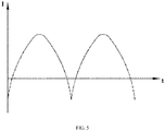
FIG. 5 is an output waveform diagram of a direct current voltage conversion circuit in a charging circuit; -
FIG. 6 is a flowchart of a charging method according to an embodiment of the present disclosure; -
FIG. 7 is a flowchart of a charging method according to another embodiment of the present disclosure; -
FIG. 8 is a line chart of charging time of a charging device according to an embodiment of the present disclosure; and -
FIG. 9 is a line chart of charging time of the existing charging device. - The present disclosure is described below in detail with reference to the accompanying drawings and specific embodiments.
-
FIG.1 exemplarily illustrates a structure diagram of acharging device 100. Abattery pack 200 is detachably connected to thecharging device 100, and is connected to an external power supply through thecharging device 100 to charge thebattery pack 200. Thecharging device 100 includes an alternatingcurrent plug 10 connected to an alternating current mains supply. The current coming from the alternating current mains supply is converted to a direct current by acharging circuit 120 in thecharging device 100 to charge thebattery pack 200. - The
charging circuit 120 illustrated inFIG. 2 includes apower supply circuit 130, an alternatingcircuit conversion circuit 140, atransformer 150 and a direct currentvoltage conversion circuit 160. - The
charging device 100 includes afirst access terminal 111 and asecond access terminal 112. Thefirst access terminal 111 and thesecond access terminal 112 constitute an input end of thecharging device 100. Thecharging device 100 further includes afirst outlet terminal 113 and asecond outlet terminal 114. Thefirst outlet terminal 113 and thesecond outlet terminal 114 constitute an output end of thecharging device 100. Thefirst access terminal 111 and thesecond access terminal 112 are connected to an alternating current voltage source, and the input alternating current voltage is loaded between thefirst access terminal 111 and thesecond access terminal 112. Specifically, the input alternating current voltage is the voltage of a power grid. Thefirst access terminal 111 and thesecond access terminal 112 are respectively connected to the alternating current plug 110. An input current is supplied to thecharging device 100 through thefirst access terminal 111 and thesecond access terminal 112, and the input current is a sinusoidal alternating current. - The
first outlet terminal 113 and thesecond outlet terminal 114 are connected to the electric energy storage or thebattery pack 200 which needs to be charged, so as to charge the electric energy storage or thebattery pack 200 accordingly. - The
first access terminal 111 and thesecond access terminal 112 are connected to thepower supply circuit 130, and thepower supply circuit 130 is connected to a first alternatingcurrent access terminal 141 and a second alternatingcurrent access terminal 142 at the output side of thepower supply circuit 130. The alternating current voltage loaded between thefirst access terminal 111 and thesecond access terminal 112 is rectified by thepower supply circuit 130 and converted to a unidirectional pulsating direct current voltage. Thepower supply circuit 130 outputs the pulsating direct current voltage at the output side. That is, the unidirectional pulsating direct current voltage is loaded between the first alternatingcurrent access terminal 141 and the second alternatingcurrent access terminal 142. Thepower supply circuit 130 is a bridge rectifier circuit, a half-wave rectifier circuit or a full wave rectifier circuit. Thepower supply circuit 130 in the embodiment is a bridge rectifier circuit. - The
charging device 100 further includes an alternatingcurrent conversion circuit 140 and acontroller 170. The alternatingcurrent conversion circuit 140 includes the first alternatingcurrent access terminal 141 and the second alternatingcurrent access terminal 142. The first alternatingcurrent access terminal 141 and the second alternatingcurrent access terminal 142, serving as the input side of the alternatingcurrent conversion circuit 140, are connected to the output side of thepower supply circuit 130. The alternatingcurrent conversion circuit 140 further includes a first alternatingcurrent outlet terminal 143 and a second alternatingcurrent outlet terminal 144. The first alternatingcurrent outlet terminal 143 and the second alternatingcurrent outlet terminal 144, serving as the output side of the alternatingcurrent conversion circuit 140, output a first alternating current with a preset frequency value. The alternatingcurrent conversion circuit 140, under the control of acontroller 170, converts the unidirectional pulsating direct current loaded between the first alternatingcurrent access terminal 141 and the second alternatingcurrent access terminal 142 to the first alternating current with a preset frequency value. - Specifically, the alternating
current conversion circuit 140 includes a first capacitor C1, a second capacitor C2, a first semiconductor switch Q1 and a second semiconductor switch Q2. One terminal of the first capacitor C1 is connected to the first alternatingcurrent access terminal 141. The other terminal of the first capacitor C1 is connected to one terminal of the second capacitor C2. The other end of the second capacitor C2 is connected to the second alternatingcurrent access terminal 142. A first terminal of the first semiconductor switch Q1 is connected to the first alternatingcurrent access terminal 141. A second terminal of the first semiconductor switch Q1 is connected to a first terminal of the second semiconductor switch Q2. A second terminal of the second semiconductor switch Q2 is connected to the second alternatingcurrent access terminal 142. The first alternatingcurrent outlet terminal 143 is connected to a node between the first capacitor C1 and the second capacitor C2 and the second alternatingcurrent outlet terminal 144 is connected to a node between the second terminal of the first semiconductor switch Q1 and the first terminal of the second semiconductor switch Q2. Each of the first semiconductor switch Q1 and the second semiconductor switch Q2 has a third terminal configured to receive the control signal from thecontroller 170. Thecontroller 170 sends a control signal to switch on one of the first semiconductor switch Q1 and the second semiconductor switch Q2 and switch off the other one. As such, the alternatingcurrent conversion circuit 140 converts the unidirectional pulsating direct current voltage to the first alternating current with the preset frequency value. The first semiconductor switch Q1 and the second semiconductor switch Q2 are MOSFETs or IGBTs. - Specifically, the
controller 170 first sends a first control signal to switch on the first semiconductor switch Q1 and switch off the second semiconductor switch Q2, and then sends a second control signal to switch off the first semiconductor switch Q1 and switch on the second semiconductor switch Q2. Thecontroller 170 alternately sends the first control signal and the second control signal to convert the pulse power supply to the first alternating current. - In a possible embodiment illustrated in
FIG.3 , a small electrolytic capacitor CY is connected between thepower supply circuit 130 and the alternating currentvoltage conversion circuit 140. The value range of the small electrolytic capacitor CY is 330 nF < CY < (0.5*output power) nF, and the output power here refers to the output power of the charging device. For example, if the output power of the charging device is 45W, the value of the small electrolytic capacitor ranges from 330 nF to 22.5 nF. - Compared with the existing
charging device 100, the difference is that there's no need to use a large electrolytic capacitor with a short service life and a large volume between thepower supply circuit 130 and the alternating current voltage conversion circuit in the embodiment, which reduces the cost of production and makes thecharging device 100 more compact. - The charging
device 100 also includes atransformer 150. Thetransformer 150 includes a primary coil M1 and a secondary coil M2. The primary coil M1 includes a firstprimary terminal 151 and a secondprimary terminal 152. The firstprimary terminal 151 is connected to the first alternatingcurrent outlet terminal 143, and the secondprimary terminal 152 is connected to the second alternatingcurrent outlet terminal 144. That is, the first alternating current is loaded between the firstprimary terminal 151 and the secondprimary terminal 152. The secondary coil M2 includes a firstsecondary terminal 153 and a secondsecondary terminal 154. The firstsecondary terminal 153 and the secondsecondary terminal 154, serving as the output side of thetransformer 150, are connected to an alternating currentvoltage conversion circuit 160. Thetransformer 150 is configured to convert the first alternating current to the second alternating current. The voltage value corresponding to the second alternating current is less than the voltage value corresponding to the first alternating current. Specifically, thetransformer 150 has two secondary coils M2, which are connected with each other head-to-tail. Specifically, thetransformer 150 is an electronic isolation transformer. - The charging
device 100 also includes the direct currentvoltage conversion circuit 160. The direct currentvoltage conversion circuit 160 includes a first directcurrent access terminal 161 and a second directcurrent access terminal 162. The first directcurrent access terminal 161 is connected to the firstsecondary terminal 153, and the second directcurrent access terminal 162 is connected to the secondsecondary terminal 154. That is, the second alternating current is loaded between the first directcurrent access terminal 161 and the second directcurrent access terminal 162. Specifically, the direct currentvoltage conversion circuit 160 includes a filter circuit and a rectifier unit. The rectifier unit consists of a first diode D1 and a second diode D2. The filter circuit includes an inductor L and a third capacitor C3. The anode of the first diode D1 is connected to the firstsecondary terminal 153. The cathode of the first diode D1 is connected to one terminal of the inductor L. The other terminal of the inductor L is connected to thefirst outlet terminal 113. The anode of the second diode D2 is connected to the secondsecondary terminal 154 and the cathode of the first diode D2 is connected to one terminal of the inductor L. One terminal of the third capacitor C3 is connected to the other terminal of the capacitor L and the other terminal of the third capacitor C3 is connected to a node between two primary coils M2. That is, the other terminal of the third capacitor C3 is connected to thesecond outlet terminal 114. The second alternating current is filtered by the unidirectional conduction characteristic of the first diode D1 and the second diode D2, and the filter circuit consisting of the inductor L and the third capacitor C3 enables the second alternating current to be filtered, such that thefirst outlet terminal 113 and thesecond outlet terminal 114 output a direct current voltage with a fluctuating waveform to charge thebattery pack 200. - It should be illustrated that the direct current with a fluctuating waveform here indicates that the waveform of the direct current output by the
first outlet terminal 113 and thesecond outlet terminal 114 is a waveform which fluctuates within a preset range, such as a sinusoidal half-wave waveform or a direct current waveform illustrated inFIG.4 . - Because the voltage of the
battery pack 200 is set with respect to thebattery pack 200 in advance, the output voltage between thefirst outlet terminal 113 and thesecond outlet terminal 114 remains substantially stable, while the output current is variable. Therefore, the output power, which is output to thebattery pack 200 by the chargingdevice 100, can be dynamically adjusted by adjusting the output current of the direct currentvoltage conversion circuit 160. - The charging
device 100 includes adetection module 180. Thedetection module 180 is connected to a node between the inductor L and thefirst outlet terminal 113, and is configured to detect the output current of the chargingcircuit 120. Thecontroller 170 outputs a corresponding control signal to the first semiconductor switch Q1 and the second semiconductor switch Q2 according to the output current detected by thedetection module 180. Alternatively, thedetection module 180 may be connected to thebattery pack 200 to detect the charging current for thebattery pack 200. Thecontroller 170 outputs a corresponding control signal according to the charging current detected by thedetection module 180 to switch on or switch off the first semiconductor switch Q1 and the second semiconductor switch Q2. - In one embodiment of the present disclosure, the
detection module 180 collects the charging current. Thecontroller 170 presets an allowable charging current reference value. Thecontroller 170 receives the effective charging current value collected by thedetection module 180, and compares the effective charging current value collected by thedetection module 180 with the preset charging current reference value, so as to compensate, rectify and output the control signal with a constant duty cycle to the first semiconductor switch Q1 and the second semiconductor switch Q2. Specifically, thecontroller 170 simultaneously outputs a control signal to switch on the first semiconductor switch Q1 and switch off the second semiconductor switch Q2. The frequency the switch-on and switch off of the first semiconductor switch Q1 is controlled in a manner of pulse width modulation with a constant duty cycle. - As illustrated in
FIG.6 , the charging method for the charging device includes steps described below. - In step S601, an effective charging current value is detected.
- In step S602, the effective charging current value is compared with a preset reference current value; if the effective charging current value is larger than the preset reference current value, going to step S603; if the effective charging current value is less than the preset reference current value, going to step S604.
- In step S603, a control signal with a decreased duty cycle is output to the first semiconductor switch Q1 and the second semiconductor switch Q2.
- In step S604, the control signal with an increased duty cycle is output to the first semiconductor switch Q1 and the second semiconductor switch Q2.
- In step S605, it is judged whether the effective charging current value is equal to the preset reference current value or not; if the effective charging current value is equal to the preset reference current value, going to step S606; if not, returning to S602;
- In step S606, the charging is performed with the preset reference current value.
- In step S601, specifically, the sampling frequency of collecting the charging current value of the battery pack by the detection module is 100HZ. The effective charging current value may be collected by the detection module from the charging device, or may be collected from the battery pack.
- In another embodiment of the present disclosure, the
detection module 180 collects the charging current peak. Thecontroller 170 presets a reference current peak. Thecontroller 170 receives the charging current peak connected by thedetection module 180 and compares the charging current peak collected by thedetection module 180 with the preset reference current peak to compensate, rectify and output the control signal with a varying duty cycle to the first semiconductor Q1 and the second semiconductor Q2, so as to output the charging current with a value close to the preset reference current peak. - As illustrated in
FIG.7 , another charging method for the charging device includes the steps described below. - In step S701, an effective charging current peak is detected.
- In step S702, the effective charging current peak is compared with a preset reference current peak; if the effective charging current peak is larger than the preset reference current peak, going to step S603; if the effective charging current peak is less than the preset reference current peak, going to step S604.
- In step S703, a control signal with a decreased duty cycle is output to the first semiconductor switch Q1 and the second semiconductor switch Q2.
- In step S704, the control signal with an increased duty cycle is output to the first semiconductor switch Q1 and the second semiconductor switch Q2.
- In step S705, it is judged whether the effective charging current peak is equal to the preset reference current peak or not; if the effective charging current peak is equal to the preset reference current peak, going to step S706; if not, returning to step S702.
- In step S706, the charging is performed with the preset reference peak.
- In step S701, specifically, the sampling frequency of collecting the charging current value of the battery pack by the detection module is 50 kHz. The effective charging current peak may be collected by the detection module from the charging device, or may be collected from the battery pack.
- The the circuit diagram of another charging
circuit 220 illustrated inFIG.4 differs from a chargingcircuit 120 illustrated inFIG. 4 is that an alternating currentvoltage conversion circuit 240 includes four semiconductor switches k1, k2, k3 and k4. Asecond outlet terminal 224 is connected to a secondsecondary terminal 254. Acontroller 270 outputs a corresponding control signal for controlling the four semiconductor switches, such that the alternating currentvoltage conversion circuit 240 converts the unidirectional pulsating direct current to the first alternating current with a preset frequency value. - A charging method for charging the electric energy storage includes the steps described below.
- In step S1, an alternating current power supply is accessed.
- In step S2, a current from the alternating current power supply is converted to a first alternating current with a preset frequency value.
- In step S3, the first alternating current is converted to a direct current with a fluctuating waveform, so as to charge the electric energy storage.
- In step S2, the alternating current power supply is converted to the first alternating current with a preset frequency by adjusting the duty cycle.
-
FIG.8 illustrates a line chart illustrating the charging of the charging device using the above charging circuit and charging method. In the line chart, the horizontal coordinate represents the charging time and the vertical coordinate represents the charging current and charging voltage. -
FIG.9 illustrates a line chart illustrating the charging of the existing charging device. In the line chart, the horizontal coordinate represents the charging time and the vertical coordinate represents the charging current and charging voltage. - Compared
FIG.8 withFIG.9 , when charging the charging device of the present disclosure and the existing charging device with a same charging current, the charging time of the charging device of the present disclosure is 4320s, while the charging time of the existing charging device is 5220s. Apparently, the charging device of the present disclosure has a high charging efficiency. - The above illustrates and describes the basic principle, main features and advantages of the present disclosure. The skilled person in the art should understand that the above embodiments does not limit the present disclosure in any form, and any technical solutions obtained by using equivalent substitution or equivalent transformation all fall within the protection scope of the present disclosure.
Claims (10)
- A charging device for charging an electric energy storage, comprising:a power supply circuit, which is connected to a power supply;an alternating current conversion circuit, which is configured to convert a current from the power supply connected to the power supply circuit to a first alternating current with a preset frequency value;a transformer, which is configured to convert the first alternating current to a second alternating current, wherein a voltage value corresponding to the second alternating current is less than a voltage value corresponding to the first alternating current; anda direct current voltage conversion circuit, which is configured to convert the second alternating current to a direct current with a waveform fluctuating in a preset range, so as to charge the electric energy storage,wherein the alternating current conversion circuit is connected to the power supply circuit, the transformer is connected to the alternating current conversion circuit, and the direct current voltage conversion circuit is connected to the transformer.
- The charging device according to claim 1, wherein the alternating current conversion circuit comprises a switching arrangement, the switching arrangement is configured to switch on or switch off a connection between the power supply circuit and the alternating current conversion circuit;
wherein the charging device further comprises a controller, the controller is configured to control a frequency of the switch-on and switch-off of the switching arrangement, so as to convert the current from the power supply connected to the power supply circuit to the first alternating current with the preset frequency value. - The charging device according to claim 2, further comprising:a detection module, which is configured to detect an output current of the direct current voltage conversion circuit; anda controller, which is configured to output a control signal with a constant duty cycle to the switching arrangement when the output current reaches a preset current value.
- The charging device according to claim 2, further comprising:a detection module, which is configured to detect an output current of the direct current voltage conversion circuit; anda controller, which is configured to output a control signal with a varying duty cycle to the switching arrangement according to a variation in the output current, so as to maintain the output current at a preset value.
- The charging device according to claim 2, wherein the direct current voltage conversion circuit comprises:a rectifier unit, which is configured to convert the second alternating current to a pulsating direct current; anda filter circuit, which is configured to convert the pulsating direct current to a smooth direct current, so as to charge the electric energy storage.
- The charging device according to claim 2, wherein the alternating current conversion circuit further comprises:a switching arrangement, which is configured to switch on a connection between the power supply circuit and the alternating current conversion circuit; anda capacitor, which is configured to constitute a current loop with the switching arrangement and the transformer during the switch-on of the switching arrangement.
- The charging device according to claim 1, wherein the current from the power supply connected to the power supply circuit is an alternating current.
- The charging device according to claim 1, wherein the transformer is a high-frequency transformer, the high-frequency ranges from 5 kHz to 1 MHz.
- A charging method for charging an electric energy storage, comprising:detecting an effective charging current value; andcomparing the effective charging current value with a preset reference current value; when the effective charging current value is larger than the preset reference current value, decreasing a duty cycle; when the effective charging current value is less than the preset reference current value, increasing the duty cycle.
- A charging method for charging an electric energy storage, comprising:detecting an effective charging current peak; andcomparing the effective charging current peak with a preset reference current peak; when the effective charging current peak is larger than the preset reference current peak, decreasing a duty cycle; when the effective charging current peak is less than the preset reference current peak, increasing the duty cycle.
Applications Claiming Priority (1)
| Application Number | Priority Date | Filing Date | Title |
|---|---|---|---|
| CN201710654317.0A CN109391016B (en) | 2017-08-03 | 2017-08-03 | Charging device and charging method |
Publications (1)
| Publication Number | Publication Date |
|---|---|
| EP3439134A1 true EP3439134A1 (en) | 2019-02-06 |
Family
ID=62748826
Family Applications (1)
| Application Number | Title | Priority Date | Filing Date |
|---|---|---|---|
| EP18179064.3A Ceased EP3439134A1 (en) | 2017-08-03 | 2018-06-21 | Charging device and charging method |
Country Status (3)
| Country | Link |
|---|---|
| US (1) | US10923938B2 (en) |
| EP (1) | EP3439134A1 (en) |
| CN (1) | CN109391016B (en) |
Citations (5)
| Publication number | Priority date | Publication date | Assignee | Title |
|---|---|---|---|---|
| US20020060552A1 (en) * | 2000-11-17 | 2002-05-23 | Hitachi Koki Co., Ltd. | Battery charger capable of accurately determining fully charged condition regardless of batteries with different charge chracteristics |
| EP1919070A2 (en) * | 2006-10-31 | 2008-05-07 | TDK Corporation | Switching power supply unit |
| EP2568569A2 (en) * | 2011-09-12 | 2013-03-13 | Panasonic Corporation | Charger |
| US20130113439A1 (en) * | 2010-04-08 | 2013-05-09 | Juergen Mack | Method and Device for Charging a Battery |
| US20130221903A1 (en) * | 2012-02-28 | 2013-08-29 | Samsung Sdi Co., Ltd. | Battery charging device and method |
Family Cites Families (10)
| Publication number | Priority date | Publication date | Assignee | Title |
|---|---|---|---|---|
| CN2502442Y (en) * | 2001-07-21 | 2002-07-24 | 常州市拓时电器有限公司 | Fast charger |
| CN1688076A (en) * | 2005-03-11 | 2005-10-26 | 周熙文 | Negative pulse charging emergency power supply |
| JP2008295172A (en) * | 2007-05-23 | 2008-12-04 | Canon Inc | Battery pack, charger and electronic apparatus |
| CN100496849C (en) * | 2007-06-18 | 2009-06-10 | 华南理工大学 | High frequency inverted direct-current spot-welding power supply device and its application |
| CN203722492U (en) * | 2014-01-14 | 2014-07-16 | 华北电力大学 | Novel switch stabilized voltage power supply |
| CN104333231A (en) * | 2014-10-31 | 2015-02-04 | 北京无线电测量研究所 | LCC serial-parallel resonant power supply and method for increasing switching frequency by power supply |
| CN105486101B (en) * | 2016-01-19 | 2017-11-17 | 河南三特炉业科技有限公司 | A kind of controllable inversion high temperature furnace |
| CN105811785A (en) * | 2016-05-23 | 2016-07-27 | 镇江天力变压器有限公司 | Transformer distribution parameter based LCC resonant type electrostatic precipitator high-frequency high-voltage power supply |
| CN106385092A (en) * | 2016-10-31 | 2017-02-08 | 江苏华航威泰机器人科技有限公司 | Robot intelligent charging system |
| US10447090B1 (en) * | 2016-11-17 | 2019-10-15 | Apple Inc. | Inductive power receiver |
-
2017
- 2017-08-03 CN CN201710654317.0A patent/CN109391016B/en active Active
-
2018
- 2018-06-21 EP EP18179064.3A patent/EP3439134A1/en not_active Ceased
- 2018-06-21 US US16/014,603 patent/US10923938B2/en active Active
Patent Citations (5)
| Publication number | Priority date | Publication date | Assignee | Title |
|---|---|---|---|---|
| US20020060552A1 (en) * | 2000-11-17 | 2002-05-23 | Hitachi Koki Co., Ltd. | Battery charger capable of accurately determining fully charged condition regardless of batteries with different charge chracteristics |
| EP1919070A2 (en) * | 2006-10-31 | 2008-05-07 | TDK Corporation | Switching power supply unit |
| US20130113439A1 (en) * | 2010-04-08 | 2013-05-09 | Juergen Mack | Method and Device for Charging a Battery |
| EP2568569A2 (en) * | 2011-09-12 | 2013-03-13 | Panasonic Corporation | Charger |
| US20130221903A1 (en) * | 2012-02-28 | 2013-08-29 | Samsung Sdi Co., Ltd. | Battery charging device and method |
Also Published As
| Publication number | Publication date |
|---|---|
| CN109391016A (en) | 2019-02-26 |
| US10923938B2 (en) | 2021-02-16 |
| US20190044364A1 (en) | 2019-02-07 |
| CN109391016B (en) | 2021-10-22 |
Similar Documents
| Publication | Publication Date | Title |
|---|---|---|
| US9214854B2 (en) | Total harmonic current distortion control circuit and method thereof | |
| CN108736727B (en) | Power converter and control method thereof | |
| US10847999B2 (en) | Wireless power receiver, wireless power transmission system using the same, and rectifier | |
| CN101499675A (en) | Charging circuit and power supply system | |
| CN110995025A (en) | Switching power supply circuit | |
| EP4175151A1 (en) | Power source providing apparatus, and charging method and system | |
| EP4047805B1 (en) | Controller and control system for dc/dc converter | |
| WO2022142803A1 (en) | Power supply apparatus, and charging method and system | |
| CN102223064B (en) | Serial resonant converter having overload delay mechanism and short-circuit protection mechanism | |
| WO2020051775A1 (en) | Power supply providing device and charging control method | |
| CN110380619B (en) | Direct current conversion circuit, control method thereof and direct current conversion device | |
| CN112803780A (en) | Converter and power adapter | |
| JP2021035267A (en) | Non-contact power supply device | |
| CN210351019U (en) | Direct current transformation circuit and inverter | |
| TWI551024B (en) | Ac-dc power conversion device and control method thereof | |
| KR101564004B1 (en) | AC-DC converter | |
| EP3439134A1 (en) | Charging device and charging method | |
| CN201656537U (en) | Accumulator charger | |
| TW202315289A (en) | Control method, controller, and control system | |
| CN211266788U (en) | Switching power supply circuit | |
| US10673322B1 (en) | Power factor correction zero current detection | |
| CN210075087U (en) | Direct current conversion circuit and direct current conversion device with high conversion efficiency | |
| CN203801099U (en) | Power circuit and microwave oven | |
| CN110572043B (en) | Direct current voltage transformation control method, direct current voltage transformation circuit and inverter | |
| KR20130001031U (en) | Power adjustable and transformerless ac to dc power circuit |
Legal Events
| Date | Code | Title | Description |
|---|---|---|---|
| PUAI | Public reference made under article 153(3) epc to a published international application that has entered the european phase |
Free format text: ORIGINAL CODE: 0009012 |
|
| STAA | Information on the status of an ep patent application or granted ep patent |
Free format text: STATUS: THE APPLICATION HAS BEEN PUBLISHED |
|
| AK | Designated contracting states |
Kind code of ref document: A1 Designated state(s): AL AT BE BG CH CY CZ DE DK EE ES FI FR GB GR HR HU IE IS IT LI LT LU LV MC MK MT NL NO PL PT RO RS SE SI SK SM TR |
|
| AX | Request for extension of the european patent |
Extension state: BA ME |
|
| STAA | Information on the status of an ep patent application or granted ep patent |
Free format text: STATUS: REQUEST FOR EXAMINATION WAS MADE |
|
| 17P | Request for examination filed |
Effective date: 20190314 |
|
| RBV | Designated contracting states (corrected) |
Designated state(s): AL AT BE BG CH CY CZ DE DK EE ES FI FR GB GR HR HU IE IS IT LI LT LU LV MC MK MT NL NO PL PT RO RS SE SI SK SM TR |
|
| STAA | Information on the status of an ep patent application or granted ep patent |
Free format text: STATUS: EXAMINATION IS IN PROGRESS |
|
| 17Q | First examination report despatched |
Effective date: 20190426 |
|
| STAA | Information on the status of an ep patent application or granted ep patent |
Free format text: STATUS: EXAMINATION IS IN PROGRESS |
|
| STAA | Information on the status of an ep patent application or granted ep patent |
Free format text: STATUS: EXAMINATION IS IN PROGRESS |
|
| STAA | Information on the status of an ep patent application or granted ep patent |
Free format text: STATUS: THE APPLICATION HAS BEEN REFUSED |
|
| 18R | Application refused |
Effective date: 20221105 |