EP3439054A1 - Display device and method for manufacturing the same - Google Patents
Display device and method for manufacturing the same Download PDFInfo
- Publication number
- EP3439054A1 EP3439054A1 EP18186697.1A EP18186697A EP3439054A1 EP 3439054 A1 EP3439054 A1 EP 3439054A1 EP 18186697 A EP18186697 A EP 18186697A EP 3439054 A1 EP3439054 A1 EP 3439054A1
- Authority
- EP
- European Patent Office
- Prior art keywords
- substrate
- layer
- display device
- buffer layer
- substrates
- Prior art date
- Legal status (The legal status is an assumption and is not a legal conclusion. Google has not performed a legal analysis and makes no representation as to the accuracy of the status listed.)
- Granted
Links
Images





Classifications
-
- H—ELECTRICITY
- H10—SEMICONDUCTOR DEVICES; ELECTRIC SOLID-STATE DEVICES NOT OTHERWISE PROVIDED FOR
- H10K—ORGANIC ELECTRIC SOLID-STATE DEVICES
- H10K71/00—Manufacture or treatment specially adapted for the organic devices covered by this subclass
- H10K71/80—Manufacture or treatment specially adapted for the organic devices covered by this subclass using temporary substrates
-
- H—ELECTRICITY
- H10—SEMICONDUCTOR DEVICES; ELECTRIC SOLID-STATE DEVICES NOT OTHERWISE PROVIDED FOR
- H10K—ORGANIC ELECTRIC SOLID-STATE DEVICES
- H10K50/00—Organic light-emitting devices
- H10K50/80—Constructional details
- H10K50/84—Passivation; Containers; Encapsulations
- H10K50/841—Self-supporting sealing arrangements
-
- H—ELECTRICITY
- H10—SEMICONDUCTOR DEVICES; ELECTRIC SOLID-STATE DEVICES NOT OTHERWISE PROVIDED FOR
- H10K—ORGANIC ELECTRIC SOLID-STATE DEVICES
- H10K50/00—Organic light-emitting devices
- H10K50/80—Constructional details
- H10K50/84—Passivation; Containers; Encapsulations
- H10K50/842—Containers
- H10K50/8426—Peripheral sealing arrangements, e.g. adhesives, sealants
-
- H—ELECTRICITY
- H10—SEMICONDUCTOR DEVICES; ELECTRIC SOLID-STATE DEVICES NOT OTHERWISE PROVIDED FOR
- H10K—ORGANIC ELECTRIC SOLID-STATE DEVICES
- H10K50/00—Organic light-emitting devices
- H10K50/80—Constructional details
- H10K50/84—Passivation; Containers; Encapsulations
- H10K50/844—Encapsulations
-
- H—ELECTRICITY
- H10—SEMICONDUCTOR DEVICES; ELECTRIC SOLID-STATE DEVICES NOT OTHERWISE PROVIDED FOR
- H10K—ORGANIC ELECTRIC SOLID-STATE DEVICES
- H10K59/00—Integrated devices, or assemblies of multiple devices, comprising at least one organic light-emitting element covered by group H10K50/00
- H10K59/10—OLED displays
- H10K59/12—Active-matrix OLED [AMOLED] displays
-
- H—ELECTRICITY
- H10—SEMICONDUCTOR DEVICES; ELECTRIC SOLID-STATE DEVICES NOT OTHERWISE PROVIDED FOR
- H10K—ORGANIC ELECTRIC SOLID-STATE DEVICES
- H10K59/00—Integrated devices, or assemblies of multiple devices, comprising at least one organic light-emitting element covered by group H10K50/00
- H10K59/30—Devices specially adapted for multicolour light emission
- H10K59/35—Devices specially adapted for multicolour light emission comprising red-green-blue [RGB] subpixels
-
- H—ELECTRICITY
- H10—SEMICONDUCTOR DEVICES; ELECTRIC SOLID-STATE DEVICES NOT OTHERWISE PROVIDED FOR
- H10K—ORGANIC ELECTRIC SOLID-STATE DEVICES
- H10K59/00—Integrated devices, or assemblies of multiple devices, comprising at least one organic light-emitting element covered by group H10K50/00
- H10K59/80—Constructional details
- H10K59/87—Passivation; Containers; Encapsulations
- H10K59/871—Self-supporting sealing arrangements
- H10K59/8722—Peripheral sealing arrangements, e.g. adhesives, sealants
-
- H—ELECTRICITY
- H10—SEMICONDUCTOR DEVICES; ELECTRIC SOLID-STATE DEVICES NOT OTHERWISE PROVIDED FOR
- H10K—ORGANIC ELECTRIC SOLID-STATE DEVICES
- H10K59/00—Integrated devices, or assemblies of multiple devices, comprising at least one organic light-emitting element covered by group H10K50/00
- H10K59/80—Constructional details
- H10K59/87—Passivation; Containers; Encapsulations
- H10K59/873—Encapsulations
-
- H—ELECTRICITY
- H10—SEMICONDUCTOR DEVICES; ELECTRIC SOLID-STATE DEVICES NOT OTHERWISE PROVIDED FOR
- H10K—ORGANIC ELECTRIC SOLID-STATE DEVICES
- H10K71/00—Manufacture or treatment specially adapted for the organic devices covered by this subclass
-
- H—ELECTRICITY
- H10—SEMICONDUCTOR DEVICES; ELECTRIC SOLID-STATE DEVICES NOT OTHERWISE PROVIDED FOR
- H10K—ORGANIC ELECTRIC SOLID-STATE DEVICES
- H10K77/00—Constructional details of devices covered by this subclass and not covered by groups H10K10/80, H10K30/80, H10K50/80 or H10K59/80
- H10K77/10—Substrates, e.g. flexible substrates
- H10K77/111—Flexible substrates
-
- B—PERFORMING OPERATIONS; TRANSPORTING
- B32—LAYERED PRODUCTS
- B32B—LAYERED PRODUCTS, i.e. PRODUCTS BUILT-UP OF STRATA OF FLAT OR NON-FLAT, e.g. CELLULAR OR HONEYCOMB, FORM
- B32B2307/00—Properties of the layers or laminate
- B32B2307/40—Properties of the layers or laminate having particular optical properties
- B32B2307/412—Transparent
-
- B—PERFORMING OPERATIONS; TRANSPORTING
- B32—LAYERED PRODUCTS
- B32B—LAYERED PRODUCTS, i.e. PRODUCTS BUILT-UP OF STRATA OF FLAT OR NON-FLAT, e.g. CELLULAR OR HONEYCOMB, FORM
- B32B2307/00—Properties of the layers or laminate
- B32B2307/70—Other properties
- B32B2307/726—Permeability to liquids, absorption
- B32B2307/7265—Non-permeable
-
- B—PERFORMING OPERATIONS; TRANSPORTING
- B32—LAYERED PRODUCTS
- B32B—LAYERED PRODUCTS, i.e. PRODUCTS BUILT-UP OF STRATA OF FLAT OR NON-FLAT, e.g. CELLULAR OR HONEYCOMB, FORM
- B32B2457/00—Electrical equipment
- B32B2457/20—Displays, e.g. liquid crystal displays, plasma displays
- B32B2457/206—Organic displays, e.g. OLED
-
- B—PERFORMING OPERATIONS; TRANSPORTING
- B32—LAYERED PRODUCTS
- B32B—LAYERED PRODUCTS, i.e. PRODUCTS BUILT-UP OF STRATA OF FLAT OR NON-FLAT, e.g. CELLULAR OR HONEYCOMB, FORM
- B32B27/00—Layered products comprising a layer of synthetic resin
- B32B27/28—Layered products comprising a layer of synthetic resin comprising synthetic resins not wholly covered by any one of the sub-groups B32B27/30 - B32B27/42
- B32B27/281—Layered products comprising a layer of synthetic resin comprising synthetic resins not wholly covered by any one of the sub-groups B32B27/30 - B32B27/42 comprising polyimides
-
- B—PERFORMING OPERATIONS; TRANSPORTING
- B32—LAYERED PRODUCTS
- B32B—LAYERED PRODUCTS, i.e. PRODUCTS BUILT-UP OF STRATA OF FLAT OR NON-FLAT, e.g. CELLULAR OR HONEYCOMB, FORM
- B32B7/00—Layered products characterised by the relation between layers; Layered products characterised by the relative orientation of features between layers, or by the relative values of a measurable parameter between layers, i.e. products comprising layers having different physical, chemical or physicochemical properties; Layered products characterised by the interconnection of layers
- B32B7/04—Interconnection of layers
- B32B7/12—Interconnection of layers using interposed adhesives or interposed materials with bonding properties
-
- H—ELECTRICITY
- H10—SEMICONDUCTOR DEVICES; ELECTRIC SOLID-STATE DEVICES NOT OTHERWISE PROVIDED FOR
- H10K—ORGANIC ELECTRIC SOLID-STATE DEVICES
- H10K2102/00—Constructional details relating to the organic devices covered by this subclass
- H10K2102/301—Details of OLEDs
- H10K2102/311—Flexible OLED
-
- H—ELECTRICITY
- H10—SEMICONDUCTOR DEVICES; ELECTRIC SOLID-STATE DEVICES NOT OTHERWISE PROVIDED FOR
- H10K—ORGANIC ELECTRIC SOLID-STATE DEVICES
- H10K50/00—Organic light-emitting devices
- H10K50/80—Constructional details
- H10K50/84—Passivation; Containers; Encapsulations
- H10K50/842—Containers
- H10K50/8423—Metallic sealing arrangements
-
- H—ELECTRICITY
- H10—SEMICONDUCTOR DEVICES; ELECTRIC SOLID-STATE DEVICES NOT OTHERWISE PROVIDED FOR
- H10K—ORGANIC ELECTRIC SOLID-STATE DEVICES
- H10K59/00—Integrated devices, or assemblies of multiple devices, comprising at least one organic light-emitting element covered by group H10K50/00
- H10K59/10—OLED displays
- H10K59/12—Active-matrix OLED [AMOLED] displays
- H10K59/1201—Manufacture or treatment
-
- H—ELECTRICITY
- H10—SEMICONDUCTOR DEVICES; ELECTRIC SOLID-STATE DEVICES NOT OTHERWISE PROVIDED FOR
- H10K—ORGANIC ELECTRIC SOLID-STATE DEVICES
- H10K59/00—Integrated devices, or assemblies of multiple devices, comprising at least one organic light-emitting element covered by group H10K50/00
- H10K59/80—Constructional details
- H10K59/87—Passivation; Containers; Encapsulations
- H10K59/871—Self-supporting sealing arrangements
- H10K59/8721—Metallic sealing arrangements
-
- H—ELECTRICITY
- H10—SEMICONDUCTOR DEVICES; ELECTRIC SOLID-STATE DEVICES NOT OTHERWISE PROVIDED FOR
- H10K—ORGANIC ELECTRIC SOLID-STATE DEVICES
- H10K71/00—Manufacture or treatment specially adapted for the organic devices covered by this subclass
- H10K71/851—Division of substrate
-
- Y—GENERAL TAGGING OF NEW TECHNOLOGICAL DEVELOPMENTS; GENERAL TAGGING OF CROSS-SECTIONAL TECHNOLOGIES SPANNING OVER SEVERAL SECTIONS OF THE IPC; TECHNICAL SUBJECTS COVERED BY FORMER USPC CROSS-REFERENCE ART COLLECTIONS [XRACs] AND DIGESTS
- Y02—TECHNOLOGIES OR APPLICATIONS FOR MITIGATION OR ADAPTATION AGAINST CLIMATE CHANGE
- Y02E—REDUCTION OF GREENHOUSE GAS [GHG] EMISSIONS, RELATED TO ENERGY GENERATION, TRANSMISSION OR DISTRIBUTION
- Y02E10/00—Energy generation through renewable energy sources
- Y02E10/50—Photovoltaic [PV] energy
- Y02E10/549—Organic PV cells
-
- Y—GENERAL TAGGING OF NEW TECHNOLOGICAL DEVELOPMENTS; GENERAL TAGGING OF CROSS-SECTIONAL TECHNOLOGIES SPANNING OVER SEVERAL SECTIONS OF THE IPC; TECHNICAL SUBJECTS COVERED BY FORMER USPC CROSS-REFERENCE ART COLLECTIONS [XRACs] AND DIGESTS
- Y02—TECHNOLOGIES OR APPLICATIONS FOR MITIGATION OR ADAPTATION AGAINST CLIMATE CHANGE
- Y02P—CLIMATE CHANGE MITIGATION TECHNOLOGIES IN THE PRODUCTION OR PROCESSING OF GOODS
- Y02P70/00—Climate change mitigation technologies in the production process for final industrial or consumer products
- Y02P70/50—Manufacturing or production processes characterised by the final manufactured product
Definitions
- the present disclosure relates to a display device and a method for manufacturing the same.
- LCD liquid crystal display
- OLED organic light emitting display
- Such a display device includes a display panel comprised of a substrate.
- a glass substrate is generally used to withstand high heat generated during a manufacturing process, there is a limitation in making properties of a thin profile, a light weight, and flexibility. Therefore, a flexible display device manufactured using flexible materials such as plastic, instead of an inflexible glass substrate, so as to maintain the same display property even when being bent like paper has recently emerged as a display device for a new generation and its research and development is actively in progress.
- a cutting process for cutting the substrate into cell units is required.
- a flexible substrate is formed on a base substrate made of glass or quartz material due to a flexible property of the flexible substrate. Afterwards, the flexible substrate is cut on the basis of the cell unit and the flexible substrate is separated from the base substrate, whereby the flexible display device is completed.
- defects of a display panel such as excitation of the flexible substrate and side permeability of the flexible substrate may be caused due to a difference in a margin between the process of cutting the flexible substrate and the process of cutting the base substrate.
- the present disclosure is directed to a display device and a method for manufacturing the same, which substantially obviate one or more problems due to limitations and disadvantages of the related art.
- An advantage of the present disclosure is to provide a display device and a method for manufacturing the same, in which excitation and side permeability of a flexible substrate are minimized to prevent defects of a display panel from occurring.
- a display device comprises a first substrate; a buffer layer arranged on the first substrate; a pixel array layer arranged on the buffer layer; and an encapsulation layer covering the pixel array layer, wherein the buffer layer surrounds a front surface and a side of the first substrate.
- a method for manufacturing a display device comprises the steps of (A) preparing a supporting substrate; (b) forming a plurality of first substrates spaced apart from one another on the supporting substrate; (C) forming a buffer layer covering the plurality of first substrates; (D) forming a pixel array layer on an area of the buffer layer overlapped with each of the plurality of first substrates; (E) forming an encapsulation layer covering the pixel array layer; and (F) forming a plurality of display panels by cutting the supporting substrate and the buffer layer based on cutting lines defined among the plurality of first substrates.
- one or more portions may be arranged between two other portions unless 'just' or 'direct' is used.
- a first horizontal-axis direction should not be construed to entail absolute directions, but rather only relative directions, and may have broader directionality within the range that elements of the present disclosure may functionally enable.
- the term "at least one” includes all combinations related with one or more items.
- “at least one among a first item, a second item and a third item” may include all combinations of two or more items selected from the first, second and third items as well as each item of the first, second and third items.
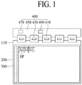
- FIG. 1 is a view illustrating a configuration of a display device according to one embodiment.
- the light emitting diode display apparatus includes a first substrate 110, and a second substrate 200.
- the first substrate 110 is a thin film transistor array substrate, and may be made of a glass or plastic material.
- the first substrate 110 includes a plurality of pixels SP.
- Each of the plurality of pixels SP is a minimum unit area where light is actually emitted, and may be defined as a sub pixel. At least three adjacent pixels SP may constitute one unit pixel for color display.
- one unit pixel may include a red pixel, a green pixel and a blue pixel, which are adjacent to one another, and may further include a white pixel for improvement of luminance.
- the second substrate 200 is arranged to cover the first substrate 110, and may be defined as an opposing substrate, a color filter array substrate, or an encapsulation substrate.
- the second substrate 200 may be bonded to the first substrate 110 by a sealant.
- the light emitting diode display apparatus further includes a gate driving circuit 300, and a panel driver 400.
- the gate driving circuit 300 generates a gate pulse in accordance with a gate signal input from the panel driver 400 and supplies the generated gate pulse to the gate line.
- the gate driving circuit 300 according to one example is built in the third non-display area of the first substrate 110 by the same process as that of the thin film transistor provided in each pixel SP.
- the gate driving circuit 300 may be provided in, but not limited to, the non-display area at a left side and/or right side of the display area.
- the gate driving circuit 300 may be provided in a random non-display area that may supply a gate pulse to the gate line.
- the gate driving circuit 300 may be manufactured in the form of a driving integrated circuit.
- the gate driving circuit 300 according to one example may be packaged in the third and/or fourth non-display area of the first substrate 110 to be connected with the plurality of gate lines one to one.
- the gate driving circuit 300 according to another example may be packaged in a gate flexible circuit film.
- the gate flexible circuit film may be attached to a gate pad portion provided in the third and/or fourth non-display area of the first substrate 110, whereby the gate driving circuit 300 may be connected to the plurality of gate lines through the gate flexible circuit film and the gate pad portion one to one.
- the panel driver 400 is connected to the pad portion provided in the first non-display area of the first substrate 110 and displays an image corresponding to image data supplied from a display driving system on the display area.
- the panel driver 400 according to one example includes a plurality of data flexible circuit films 410, a plurality of data driving integrated circuits 430, a printed circuit board 450, a timing controller 470, and a power circuit 490.
- Each of the plurality of data flexible circuit films 410 is attached to the pad portion of the first substrate 110 by a film attachment process.
- Each of the plurality of data driving integrated circuits 430 is individually packaged in each of the plurality of data flexible circuit films 410.
- the data driving integrated circuit 430 receives pixel data and data control signal provided from the timing controller 470, converts the pixel data to an analog type data voltage per pixel in accordance with the data control signal, and supplies the converted data voltage to the corresponding data line.
- the printed circuit board 450 is connected with the plurality of data flexible circuit films 410.
- the printed circuit board 450 supports the timing controller 470 and the power circuit 490, and serves to deliver a signal and a power source between elements of the panel driver 400.
- the timing controller 470 is packaged in the printed circuit board 450, and receives image data and a timing synchronization signal provided from the display driving system through a user connector provided in the printed circuit board 450.
- the timing controller 470 generates pixel data by aligning the image data to be suitable for a pixel arrangement structure of the display area on the basis of the timing synchronization signal, and provides the generated pixel data to the data driving integrated circuit 430.
- the timing controller 470 controls each driving timing of the plurality of data driving integrated circuits 430 and the gate driving circuits 300 by generating each of the data control signal and the gate control signal on the basis of the timing synchronization signal.
- the power circuit 490 is packaged in the printed circuit board 450, generates various voltages required to display an image on the display area by using externally input power source and supplies the generated voltages to the corresponding element.
- the panel driver 400 may further include a control board connected to the printed circuit board 450.
- the timing controller 470 and the power circuit 490 are packaged in the control board without being packaged in the printed circuit board 450. Therefore, the printed circuit board 450 serves to deliver a signal and a power source between the plurality of data flexible circuit films 410 and the control board.
- FIG. 2 is a cross-sectional view illustrating a display device according to one embodiment.
- the display device displays an image corresponding to a data signal provided from a driving circuit, and comprises a first substrate 110, a buffer layer 120, a passivation film 125, a pixel array layer 130, an encapsulation layer 140, a second substrate 160, and a light-transmitting film 180.
- the first substrate 110 is a base substrate, and may include a plastic material.
- the first substrate 110 may include an opaque or colored polyimide material.
- the first substrate 110 made of a polyimide material may be a hardened polyimide resin coated with a constant thickness on a front surface of a delamination layer arranged on a supporting substrate which is relatively thick.
- the supporting substrate is separated from the first substrate 110 by delamination of the delamination layer using a laser delamination process.
- the supporting substrate may also be referred to as a base substrate herein.
- the buffer layer 120 is arranged on the first substrate 110.
- the buffer layer 120 according to one embodiment serves to prevent water from being permeated into the buffer layer 120 and the pixel array layer 130.
- the buffer layer 120 may be made of an inorganic insulating material, for example, but not limited to, a silicon dioxide (SiO 2 ), a silicon nitride (SiNx) or a multi-layer of SiO 2 and SiNx.
- the buffer layer according to one embodiment is formed to surround a front surface and a side of the first substrate 110.
- the front surface is an upper surface.
- the front surface is a surface of the first substrate 110 that is closest to the second substrate 160 and/or that is closest to the pixel array layer (130).
- the front surface of the first substrate 110 is the surface of the first substrate 110 that faces the second substrate 160. If the buffer layer 120 is formed to cover only the front surface of the first substrate 110, permeability to the side of the first substrate 110 occurs, which causes a defect of the display panel. However, since the buffer layer 120 according to one embodiment is formed to surround even the side of the first substrate 110, side permeability of the first substrate 110 may be avoided, whereby the defect of the display panel may be prevented from occurring.
- the first substrate 110 is in the form of rectangular cube, also called a rectangular prism. As such, it has six sides, the front and back sides and the sidewalls that extend between the front and back sides.
- the buffer layer will surround five of these six walls. In a preferred embodiment, the buffer layer is in abutting contact with each of the five sides, which may also be called surfaces of the first substrate 110.
- the passivation film 125 is formed at the side of the first substrate 110.
- the passivation film 125 may be made of an inorganic material or metal material.
- the passivation film 125 may be formed to have a same height as that of the buffer layer 120 surrounding the side and the front surface of the first substrate 110.
- the passivation film 125 may prevent side permeability of the first substrate 110 from occurring in a similar manner to the buffer layer 120, and may serve as a dam that prevents particles such as dust from being permeated into the first substrate 110.
- the buffer layer 120 together with the passivation film 125 may protect the first substrate 110, a defect ratio of the display panel may be reduced remarkably, and therefore reliability of the display device may be improved.
- the pixel array layer 130 is arranged on the buffer layer 120 and includes a plurality of pixels for displaying an image.
- the plurality of pixels may include various kinds of elements such as a thin film transistor, a light emitting diode, a pixel electrode, etc., to provide display by the display device according to the present disclosure.
- the plurality of pixels are minimum units of area from which a light is emitted and may each comprise a light emitting diode emitting light based on a pixel driving power source provided from a driving power line.
- the light emitting diode may be an organic light emitting diode OLED, and light generated from the organic light emitting diode is emitted to the outside to display an image.
- the encapsulation layer 140 is formed to cover the pixel array layer 130 to prevent water permeation to each pixel and protect the light emitting diode vulnerable to external water or oxygen.
- the encapsulation layer 140 may be formed of an inorganic material or organic material, or may be formed of a deposition structure where an inorganic material and an organic material are deposited alternately.
- the second substrate 160 is arranged on the encapsulation layer 140 to protect the light emitting diode like the encapsulation layer 140.
- the second substrate 160 may be formed of metal with a reflective material.
- the second substrate 160 may be attached to the encapsulation layer 140 using an adhesive layer 150 disposed between the second substrate 160 and the encapsulation layer 140, which may prevent water permeation into the entire surface of the display panel.
- the second substrate 160 according to one embodiment may be formed to have a larger area than the pixel array layer 130 to effectively prevent water permeation into the entire surface of the light emitting diode.
- the adhesive layer 150 is formed to adhere and fix the encapsulation layer 140 and the second substrate 160 to each other.
- the adhesive layer 150 may perform adhesion using a hardening method of high energy such as heat, ultraviolet, and laser, or a physical pressure using a pressure-sensitive adhesive (PSA) material.
- a hardening method of high energy such as heat, ultraviolet, and laser
- PSA pressure-sensitive adhesive
- the light-transmitting film 180 is attached to a rear surface of the first substrate 110 by using a transparent adhesive material as a medium.
- the rear surface corresponds to an opposite direction to the front surface.
- the light-transmitting film 180 may be made of a flexible film, for example, at least one of a polyethylene terephthalate film, an anti-reflective film, a polarizing film, and a transmittance controllable film.
- the light-transmitting film 180 may be attached to the rear surface of the first substrate 110 that is separated from the supporting substrate.
- the transparent adhesive material may be an optically clear resin (OCR) or an optically clear adhesive (OCA).
- OCR optically clear resin
- OCA optically clear adhesive
- FIG. 3 is cross-sectional view illustrating a display device according to another embodiment, wherein the display device shown in FIG. 2 additionally includes an inorganic layer.
- the display device includes an inorganic layer 170 formed on the rear surface of the first substrate 110.
- an inorganic layer 170 formed on the rear surface of the first substrate 110.
- the inorganic layer 170 is formed on the rear surface of the first substrate 110 and protects the first substrate 110 and the light emitting diode from permeation of external particles, impact, water, and oxygen.
- the inorganic layer 170 may be formed of a single layer or a plurality of layers.
- the inorganic layer 170 may be made of an inorganic insulating material, which enables low temperature deposition, such as a silicon nitride (SiNx), a silicon oxide (SiOx), and an aluminum oxide (AlOx).
- the inorganic layer 170 is formed to prevent defects of the display panel caused by the first substrate 110 being damaged by external particles, water, etc. after being exposed to the outside when the supporting substrate is separated from the first substrate 110 by the delamination during the process of forming the display panel.
- the inorganic layer 170 is not arranged on the rear surface of the first substrate 110 separately after the display panel is formed, but arranged during the process of forming the display panel.
- the inorganic film 170 will be described later in more detail.
- FIG. 4 is a cross-sectional view illustrating a display device according to still another embodiment, wherein the display device shown in FIG. 2 includes a barrier film instead of a light-transmitting film.
- the display device includes a barrier film 190 attached to the rear surface of the first substrate 110.
- a barrier film 190 attached to the rear surface of the first substrate 110.
- the barrier film 190 is attached to the rear surface of the first substrate 110 by using a transparent adhesive material as a medium.
- the barrier film 190 may be a phase difference film or optically isotropic film. If the barrier film has optically isotropic property, light entering the barrier film 190 is transmitted without a phase delay.
- more inorganic films may be arranged on the upper surface of the barrier film.
- the inorganic film may include a silicon nitride (SiNx) and a silicon oxide (SiOx).
- SiNx silicon nitride
- SiOx silicon oxide
- the inorganic film formed on the upper surface of the barrier film 190 serves to block permeation of external water or oxygen.
- the buffer film 190 may prevent the first substrate 110 and the light emitting diode from being damaged.
- the barrier film 190 includes a liquid moisture absorbing material, and if external water is permeated into the barrier film 190, water particles are combined with the liquid moisture absorbing material and are kept in an empty space in the barrier film 190, whereby the barrier film 190 may have properties of water permeation prevention or water permeation delay.
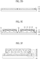
- FIGS. 5a to 5h are cross-sectional views illustrating a method for manufacturing a display device according to one embodiment. Therefore, the same reference numerals are given to the same elements, and redundant description of the repeated parts regarding elements and the structure of each element will be omitted.
- the supporting substrate 100 serves to securely support a flexible substrate so that a thin flexible substrate is not easily bent or distorted and its shape is fixed during the process of manufacturing the display device. Through such a supporting substrate 100, the flexible substrate may be used easily, and a subsequent process may be performed more precisely and securely.
- the supporting substrate 100 may be made of a transparent inorganic material such as a plate shaped glass or quartz, which has excellent heat-resistance. Although not shown, the supporting substrate 100 may have a cutting line defined among a plurality of flexible substrates.
- the first substrate 110 may be a flexible substrate including plastic materials. Since the first substrates 110 according to one embodiment are not formed on the supporting substrate 100 in a single body but formed to be spaced apart from one another, cutting of the first substrate 110 is not required when the display panel is formed through the cutting process. Therefore, the process is more simplified than the related art process that includes two steps of a process of cutting the first substrate 110 and a process of cutting the supporting substrate 100, and defects may be prevented from occurring in the cutting process due to a margin difference between the two processes.
- the passivation film 125 is formed on the supporting substrate 100.
- the passivation film 125 may be formed to be spaced apart on every side of the first substrate 110 to protect the sides of the first substrate 110.
- the passivation film 125 may serve as a dam that prevents particles such as dust generated in the cutting process for forming the display panel from being permeated into the first substrate 110.
- the buffer layer 120 surrounding the front surface and the sides of the plurality of the first substrates 110 and the passivation film 125 is formed.
- the buffer layer 120 according to one embodiment is formed to surround the side as well as the front surface of a first substrate 110. Therefore, since the side of the first substrate 110 is not exposed in the process of cutting the supporting substrate 100 and the buffer layer 120, excitation and side permeability of the first substrate 110 may be minimized.
- the buffer layer 120 protects the first substrate 110 from external damages together with the passivation film 125.
- Each substrate 110 has six sides, a large area front side, a large area back side and four sides, which are the sidewalls that extend from the front side to the back side. As can be appreciate, only four of the sides can be seen in Figure 5d , the other two sides being located behind and in front of the image shown in Figure 5d .
- the buffer layer therefore surrounds the substrate 110 on five sides. In one embodiment, the buffer layer 120 is in contact with five of the six sides of the substrate 110.
- the pixel array layer 130, the encapsulation layer 140, the adhesive layer 150, and the second substrate 160 are sequentially formed on the buffer layer 120.
- Each of the pixel array layer 130, the encapsulation layer 140, the adhesive layer 150, and the second substrate 160 may be formed on an area overlapped with each of the plurality of first substrates 110. Therefore, each of the pixel array layer 130, the encapsulation layer 140, the adhesive layer 150, and the second substrate 160 is not cut by the cutting process.
- the second substrate 160 may be attached to the encapsulation layer 140 by using an adhesive material.
- an adhesive material may be the adhesive layer 150, and may be made of resin.
- the supporting substrate 100 and the buffer layer 120 have cutting lines CL defined among the plurality of the first substrates 110.
- the cutting lines CL are lines arranged among the plurality of the first substrates 110 to designate a plurality of display panels, and a display panel cell cutting process is performed along the cutting lines CL.
- a display panel on a cell basis is formed by cutting the supporting substrate 100 and the buffer layer 120 along the cutting line(s).
- the display panel according to one embodiment does not permit permeation of water and particles into the first substrate 110 in the cutting process, a display panel having no defects may be obtained through the process according to one embodiment.
- the first substrate 110 formed on the supporting substrate 100 is separated from the supporting substrate 100 through a delamination process.
- a delamination process may comprise a laser beam being irradiated onto a silicon film provided on the supporting substrate 100, heat treatment being applied to the silicon film and then the heat-treated silicon film being subjected to dehydrogenation.
- the first substrate 110 may be separated from the supporting substrate 100.
- the light-transmitting film 180 is attached to the rear surface of the first substrate 110 that is separated from the supporting substrate 100.
- the light-transmitting film 180 may be attached to the rear surface of the first substrate 110 by a transparent adhesive material.
- the light-transmitting film 180 according to one embodiment is attached to the rear surface of the first substrate that is separated from the supporting substrate 100 to avoid deterioration of visibility due to reflection by metals inside the display panel, and has the advantage of protecting the rear surface of the first substrate 110 from the outside.
- the conventional cutting process of the first substrate 110 may be omitted, whereby the number of entire processes and time for production may be reduced, and defects in the cutting process due to a margin difference between the cutting process of the supporting substrate 100 and the cutting process of the first substrate 110 may be prevented from occurring. Also, since cracks and damage that may occur in the conventional cutting process of the first substrate 110 may be avoided, a display panel with a low defect ratio and an improved yield may be formed.
- the buffer layer covers the front surface and the sides of the plurality of the first substrates 110 formed on the supporting substrate 100, the sides of the first substrates 110 are not exposed to the outside during the cutting process, whereby excitation and permeability of the first substrate 100 may be minimized. Therefore, entire permeability of the display panel is avoided and reliability of the display panel may be improved.
- FIGS. 6a to 6h are cross-sectional views illustrating a method for manufacturing a display device according to another embodiment. Since the process of additionally forming an inorganic layer is added to the method for manufacturing the display device according to FIGS 5a to 5h , in FIGS. 6a to 6h description repeated from the FIGS 5a to 5h will be omitted and the additional process will be described.
- the inorganic layer 170 is formed on the supporting substrate 100, and a plurality of first substrates 110 is formed on the inorganic layer 170.
- the inorganic layer 170 is formed in a single body unlike the plurality of first substrates 110. This is to allow the inorganic layer 170 to have a width greater than the first substrates 110 to protect the rear surface of the first substrate 110 from the outside even if the supporting substrate 100 is separated later through the cutting process and the delamination process.
- the inorganic layer 170 serves to protect the first substrate(s) 110 by being formed on the supporting substrate 100 in advance before the first substrate(s) 110 is/are formed in order to prevent the first substrate(s) 110 from being damaged by external particles and water when the first substrate(s) 110 is/are separated from the supporting substrate 100.
- the inorganic layer 170 is formed on the supporting substrate 100, the plurality of first substrates are formed on the inorganic layer 170, and the buffer layer 120, the pixel array layer 130, the encapsulation layer 140, the adhesive layer 150, and the second substrate 160 are sequentially formed on the plurality of first substrates 110.
- the supporting substrate 100, the inorganic layer 170, and the buffer layer 120 are cut based on the cutting lines CL defined among the plurality of first substrates 110. Since the inorganic layer 170 is cut along with the supporting substrate 100 and the buffer layer 120 after being formed in a single body, the inorganic layer 170 may have a larger width than the first substrate(s) 110 and may later protect the rear surface of the first substrate(s) 110 from the outside even when the supporting substrate 100 is separated.
- the light-transmitting film 180 is attached to the rear surface of the inorganic layer 170 from which the supporting substrate 100 is separated.
- the light-transmitting film 180 may be attached to the rear surface of the inorganic layer 170 by using a transparent adhesive material.
- the light-transmitting film 180 according to one embodiment may avoid deterioration of visibility and have an advantage in protecting the rear surface of the first substrate 110 from the outside like the inorganic layer 170.
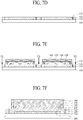
- FIGS. 7a to 7h are cross-sectional views illustrating a method for manufacturing a display device according to another embodiment. Since a barrier film, instead of the light-transmitting film described in the method according to FIGS. 5a to 5h , is attached in FIGS. 7a to 7h , description repeated from FIGS. 5a to 5h will be omitted, and the changed process will be described.
- the barrier film 190 is attached to the rear surface of the first substrate 110 separated from the supporting substrate 100.
- the barrier film 190 is attached the rear surface of the first substrate 110 using a transparent adhesive material. Since the barrier film 190 according to one embodiment has properties of being an excellent water barrier and providing impact mitigation, damage to the first substrate 110 may be avoided.
- an additional inorganic film may be arranged on the upper surface of the barrier film. The inorganic film serves to block permeation of external water or oxygen, and may be attached to the rear surface of the first substrate 110 using a transparent adhesive material. If the barrier film 190 according to one embodiment includes an inorganic film, an effect of preventing water permeation into the first substrate 110 may be improved, and reliability of the display panel may be improved.
- the display device according to the present disclosure has the following advantages.
- the display device has an advantage in preventing defects in the display panel by minimizing excitation and side permeability of the first substrate.
- the display device has an advantage in improving reliability and reducing costs for production by preventing defects in the display panel from occurring.
- the display device has an advantage in simplifying a module process and improving yield by omitting the process of cutting the first substrate.
Landscapes
- Engineering & Computer Science (AREA)
- Manufacturing & Machinery (AREA)
- Physics & Mathematics (AREA)
- Optics & Photonics (AREA)
- Microelectronics & Electronic Packaging (AREA)
- Electroluminescent Light Sources (AREA)
- Devices For Indicating Variable Information By Combining Individual Elements (AREA)
Abstract
Description
- This application claims the benefit of the Korean Patent Application No.
10-2017-0097344 filed on July, 31, 2017 - The present disclosure relates to a display device and a method for manufacturing the same.
- Recently, with the advancement of the information age, a display field for processing and displaying large amounts of information has been rapidly developed. In response to this trend, various display devices have been developed and used. Among such display devices, there is a trend that liquid crystal display (LCD) devices and organic light emitting display (OLED) devices having excellent properties of a thin profile, a light weight, and low power consumption have been widely used.
- Such a display device includes a display panel comprised of a substrate. In this case, since a glass substrate is generally used to withstand high heat generated during a manufacturing process, there is a limitation in making properties of a thin profile, a light weight, and flexibility. Therefore, a flexible display device manufactured using flexible materials such as plastic, instead of an inflexible glass substrate, so as to maintain the same display property even when being bent like paper has recently emerged as a display device for a new generation and its research and development is actively in progress.
- In order to manufacture the flexible display device, after a display element forming process is performed for forming a display element such as a thin film transistor on a large area of the flexible substrate on a basis of unit area, a cutting process for cutting the substrate into cell units is required. A flexible substrate is formed on a base substrate made of glass or quartz material due to a flexible property of the flexible substrate. Afterwards, the flexible substrate is cut on the basis of the cell unit and the flexible substrate is separated from the base substrate, whereby the flexible display device is completed.
- However, in the process of cutting the flexible substrate and the base substrate on the basis of the cell unit, defects of a display panel such as excitation of the flexible substrate and side permeability of the flexible substrate may be caused due to a difference in a margin between the process of cutting the flexible substrate and the process of cutting the base substrate.
- Aspects of the invention are set out in the independent claims.
- Accordingly, the present disclosure is directed to a display device and a method for manufacturing the same, which substantially obviate one or more problems due to limitations and disadvantages of the related art.
- An advantage of the present disclosure is to provide a display device and a method for manufacturing the same, in which excitation and side permeability of a flexible substrate are minimized to prevent defects of a display panel from occurring.
- Additional advantages and features of the disclosure will be set forth in part in the description which follows and in part will become apparent to those having ordinary skill in the art upon examination of the following or may be learned from practice of the disclosure. The objectives and other advantages of the disclosure may be realized and attained by the structure particularly pointed out in the written description and claims hereof as well as the appended drawings.
- To achieve these objects and other advantages and in accordance with the purpose of the disclosure, as embodied and broadly described herein, a display device according to the present disclosure comprises a first substrate; a buffer layer arranged on the first substrate; a pixel array layer arranged on the buffer layer; and an encapsulation layer covering the pixel array layer, wherein the buffer layer surrounds a front surface and a side of the first substrate.
- In another aspect of the present disclosure, a method for manufacturing a display device comprises the steps of (A) preparing a supporting substrate; (b) forming a plurality of first substrates spaced apart from one another on the supporting substrate; (C) forming a buffer layer covering the plurality of first substrates; (D) forming a pixel array layer on an area of the buffer layer overlapped with each of the plurality of first substrates; (E) forming an encapsulation layer covering the pixel array layer; and (F) forming a plurality of display panels by cutting the supporting substrate and the buffer layer based on cutting lines defined among the plurality of first substrates.
- It is to be understood that both the foregoing general description and the following detailed description of the present disclosure are exemplary and explanatory and are intended to provide further explanation of the disclosure.
-
- The accompanying drawings, which are included to provide a further understanding of the disclosure and are incorporated in and constitute a part of this application, illustrate embodiment(s) of the disclosure and together with the description serve to explain the principle of the disclosure. In the drawings:
-
FIG. 1 is a view illustrating a display device according to one embodiment. -
FIG. 2 is a cross-sectional view illustrating a display device according to one embodiment; -
FIG. 3 is cross-sectional view illustrating a display device according to another embodiment, wherein the display device shown inFIG. 1 additionally includes an inorganic layer; -
FIG. 4 is a cross-sectional view illustrating a display device according to still another embodiment, wherein the display device shown inFIG. 1 includes a barrier film instead of a light-transmitting film; -
FIGS. 5a to 5h are cross-sectional views illustrating a method for manufacturing a display device according to one embodiment; -
FIGS. 6a to 6h are cross-sectional views illustrating a method for manufacturing a display device according to another embodiment; and -
FIGS. 7a to 7h are cross-sectional views illustrating a method for manufacturing a display device according to another embodiment. - Advantages and features of the present disclosure, and implementation methods thereof, will be clarified through the following embodiments described with reference to the accompanying drawings. The present disclosure may, however, be embodied in different forms and should not be construed as limited to the embodiments set forth herein. Rather, these embodiments are provided so that this disclosure will be thorough and complete, and will fully convey the scope of the present disclosure to those skilled in the art.
- A shape, a size, a ratio, an angle, and a number disclosed in the drawings for describing embodiments are merely examples, and thus, the present disclosure is not limited to the illustrated details. Like reference numerals refer to like elements throughout. In the following description, when the detailed description of the relevant known function or configuration is determined to unnecessarily obscure an important point of the present disclosure, the detailed description will be omitted.
- In a case where 'comprise', 'have', and 'include' described in the present specification are used, another part may be added unless 'only∼' is used. The terms of a singular form may include plural forms unless referred to the contrary.
- In construing an element, the element is construed as including an error range although there is no explicit description.
- In describing a position relationship, for example, when the position relationship is described as 'upon∼', 'above∼', 'below∼', and 'next to∼', one or more portions may be arranged between two other portions unless 'just' or 'direct' is used.
- In describing a time relationship, for example, when the temporal order is described as 'after∼', 'subsequent∼', 'next∼', and 'before∼', a case which is not continuous may be included unless 'just' or 'direct' is used.
- It will be understood that, although the terms "first", "second", etc. may be used herein to describe various elements, these elements should not be limited by these terms. These terms are only used to distinguish one element from another element. Therefore, a first element mentioned hereinafter could be termed a second element, without departing from the scope of the present disclosure.
- "A first horizontal-axis direction", "a second horizontal-axis direction" and "a vertical-axis direction" should not be construed to entail absolute directions, but rather only relative directions, and may have broader directionality within the range that elements of the present disclosure may functionally enable.
- It should be understood that the term "at least one" includes all combinations related with one or more items. For example, "at least one among a first item, a second item and a third item" may include all combinations of two or more items selected from the first, second and third items as well as each item of the first, second and third items.
- Features of various embodiments may be partially or completely coupled to or combined with each other, and may be variously inter-operated with each other and driven technically as those skilled in the art can sufficiently understand. The embodiments may be carried out independently from each other, or may be carried out together in co-dependent relationships.
- Hereinafter, the preferred embodiments will be described in detail with reference to the accompanying drawings. In adding reference numerals to elements of respective drawings, it is to be understood that the same reference elements may have the same reference numerals if possible even though the same reference elements are shown on different drawings.
-
FIG. 1 is a view illustrating a configuration of a display device according to one embodiment. - Referring to
FIGS. 1 , the light emitting diode display apparatus according to this embodiment includes afirst substrate 110, and asecond substrate 200. - The
first substrate 110 is a thin film transistor array substrate, and may be made of a glass or plastic material. - The
first substrate 110 according to one example includes a plurality of pixels SP. - Each of the plurality of pixels SP is a minimum unit area where light is actually emitted, and may be defined as a sub pixel. At least three adjacent pixels SP may constitute one unit pixel for color display. For example, one unit pixel may include a red pixel, a green pixel and a blue pixel, which are adjacent to one another, and may further include a white pixel for improvement of luminance.
- The
second substrate 200 is arranged to cover thefirst substrate 110, and may be defined as an opposing substrate, a color filter array substrate, or an encapsulation substrate. Thesecond substrate 200 may be bonded to thefirst substrate 110 by a sealant. - Additionally, the light emitting diode display apparatus according to one example of the present invention further includes a
gate driving circuit 300, and apanel driver 400. - The
gate driving circuit 300 generates a gate pulse in accordance with a gate signal input from thepanel driver 400 and supplies the generated gate pulse to the gate line. Thegate driving circuit 300 according to one example is built in the third non-display area of thefirst substrate 110 by the same process as that of the thin film transistor provided in each pixel SP. For example, thegate driving circuit 300 may be provided in, but not limited to, the non-display area at a left side and/or right side of the display area. Thegate driving circuit 300 may be provided in a random non-display area that may supply a gate pulse to the gate line. - Selectively, the
gate driving circuit 300 may be manufactured in the form of a driving integrated circuit. In this case, thegate driving circuit 300 according to one example may be packaged in the third and/or fourth non-display area of thefirst substrate 110 to be connected with the plurality of gate lines one to one. Thegate driving circuit 300 according to another example may be packaged in a gate flexible circuit film. In this case, the gate flexible circuit film may be attached to a gate pad portion provided in the third and/or fourth non-display area of thefirst substrate 110, whereby thegate driving circuit 300 may be connected to the plurality of gate lines through the gate flexible circuit film and the gate pad portion one to one. - The
panel driver 400 is connected to the pad portion provided in the first non-display area of thefirst substrate 110 and displays an image corresponding to image data supplied from a display driving system on the display area. Thepanel driver 400 according to one example includes a plurality of dataflexible circuit films 410, a plurality of data drivingintegrated circuits 430, a printedcircuit board 450, atiming controller 470, and apower circuit 490. - Each of the plurality of data
flexible circuit films 410 is attached to the pad portion of thefirst substrate 110 by a film attachment process. - Each of the plurality of data driving
integrated circuits 430 is individually packaged in each of the plurality of dataflexible circuit films 410. The data drivingintegrated circuit 430 receives pixel data and data control signal provided from thetiming controller 470, converts the pixel data to an analog type data voltage per pixel in accordance with the data control signal, and supplies the converted data voltage to the corresponding data line. - The printed
circuit board 450 is connected with the plurality of dataflexible circuit films 410. The printedcircuit board 450 supports thetiming controller 470 and thepower circuit 490, and serves to deliver a signal and a power source between elements of thepanel driver 400. - The
timing controller 470 is packaged in the printedcircuit board 450, and receives image data and a timing synchronization signal provided from the display driving system through a user connector provided in the printedcircuit board 450. Thetiming controller 470 generates pixel data by aligning the image data to be suitable for a pixel arrangement structure of the display area on the basis of the timing synchronization signal, and provides the generated pixel data to the data drivingintegrated circuit 430. Also, thetiming controller 470 controls each driving timing of the plurality of data drivingintegrated circuits 430 and thegate driving circuits 300 by generating each of the data control signal and the gate control signal on the basis of the timing synchronization signal. - The
power circuit 490 is packaged in the printedcircuit board 450, generates various voltages required to display an image on the display area by using externally input power source and supplies the generated voltages to the corresponding element. - Additionally, the
panel driver 400 may further include a control board connected to the printedcircuit board 450. In this case, thetiming controller 470 and thepower circuit 490 are packaged in the control board without being packaged in the printedcircuit board 450. Therefore, the printedcircuit board 450 serves to deliver a signal and a power source between the plurality of dataflexible circuit films 410 and the control board. -
FIG. 2 is a cross-sectional view illustrating a display device according to one embodiment. - Referring to
FIG. 2 , the display device according to one embodiment displays an image corresponding to a data signal provided from a driving circuit, and comprises afirst substrate 110, abuffer layer 120, apassivation film 125, apixel array layer 130, anencapsulation layer 140, asecond substrate 160, and a light-transmittingfilm 180. - The
first substrate 110 is a base substrate, and may include a plastic material. In this case, if thefirst substrate 110 includes a plastic material, thefirst substrate 110 may include an opaque or colored polyimide material. For example, thefirst substrate 110 made of a polyimide material may be a hardened polyimide resin coated with a constant thickness on a front surface of a delamination layer arranged on a supporting substrate which is relatively thick. In this case, the supporting substrate is separated from thefirst substrate 110 by delamination of the delamination layer using a laser delamination process. The supporting substrate may also be referred to as a base substrate herein. - The
buffer layer 120 is arranged on thefirst substrate 110. Thebuffer layer 120 according to one embodiment serves to prevent water from being permeated into thebuffer layer 120 and thepixel array layer 130. Thebuffer layer 120 may be made of an inorganic insulating material, for example, but not limited to, a silicon dioxide (SiO2), a silicon nitride (SiNx) or a multi-layer of SiO2 and SiNx. - The buffer layer according to one embodiment is formed to surround a front surface and a side of the
first substrate 110. In this case, the front surface is an upper surface. In other words, the front surface is a surface of thefirst substrate 110 that is closest to thesecond substrate 160 and/or that is closest to the pixel array layer (130). Put another way, the front surface of thefirst substrate 110 is the surface of thefirst substrate 110 that faces thesecond substrate 160. If thebuffer layer 120 is formed to cover only the front surface of thefirst substrate 110, permeability to the side of thefirst substrate 110 occurs, which causes a defect of the display panel. However, since thebuffer layer 120 according to one embodiment is formed to surround even the side of thefirst substrate 110, side permeability of thefirst substrate 110 may be avoided, whereby the defect of the display panel may be prevented from occurring. - As can be appreciated, the
first substrate 110 is in the form of rectangular cube, also called a rectangular prism. As such, it has six sides, the front and back sides and the sidewalls that extend between the front and back sides. The buffer layer will surround five of these six walls. In a preferred embodiment, the buffer layer is in abutting contact with each of the five sides, which may also be called surfaces of thefirst substrate 110. - The
passivation film 125 is formed at the side of thefirst substrate 110. Thepassivation film 125 according to one embodiment may be made of an inorganic material or metal material. Thepassivation film 125 may be formed to have a same height as that of thebuffer layer 120 surrounding the side and the front surface of thefirst substrate 110. Thepassivation film 125 according to one embodiment may prevent side permeability of thefirst substrate 110 from occurring in a similar manner to thebuffer layer 120, and may serve as a dam that prevents particles such as dust from being permeated into thefirst substrate 110. - Since the
buffer layer 120 together with thepassivation film 125 according to one embodiment may protect thefirst substrate 110, a defect ratio of the display panel may be reduced remarkably, and therefore reliability of the display device may be improved. - The
pixel array layer 130 is arranged on thebuffer layer 120 and includes a plurality of pixels for displaying an image. The plurality of pixels according to one embodiment may include various kinds of elements such as a thin film transistor, a light emitting diode, a pixel electrode, etc., to provide display by the display device according to the present disclosure. The plurality of pixels are minimum units of area from which a light is emitted and may each comprise a light emitting diode emitting light based on a pixel driving power source provided from a driving power line. The light emitting diode according to one embodiment may be an organic light emitting diode OLED, and light generated from the organic light emitting diode is emitted to the outside to display an image. - The
encapsulation layer 140 is formed to cover thepixel array layer 130 to prevent water permeation to each pixel and protect the light emitting diode vulnerable to external water or oxygen. Theencapsulation layer 140 according to one embodiment may be formed of an inorganic material or organic material, or may be formed of a deposition structure where an inorganic material and an organic material are deposited alternately. - The
second substrate 160 is arranged on theencapsulation layer 140 to protect the light emitting diode like theencapsulation layer 140. Thesecond substrate 160 according to one embodiment may be formed of metal with a reflective material. Thesecond substrate 160 may be attached to theencapsulation layer 140 using anadhesive layer 150 disposed between thesecond substrate 160 and theencapsulation layer 140, which may prevent water permeation into the entire surface of the display panel. Thesecond substrate 160 according to one embodiment may be formed to have a larger area than thepixel array layer 130 to effectively prevent water permeation into the entire surface of the light emitting diode. - The
adhesive layer 150 is formed to adhere and fix theencapsulation layer 140 and thesecond substrate 160 to each other. Theadhesive layer 150 may perform adhesion using a hardening method of high energy such as heat, ultraviolet, and laser, or a physical pressure using a pressure-sensitive adhesive (PSA) material. - The light-transmitting
film 180 is attached to a rear surface of thefirst substrate 110 by using a transparent adhesive material as a medium. In this case, the rear surface corresponds to an opposite direction to the front surface. The light-transmittingfilm 180 according to one embodiment may be made of a flexible film, for example, at least one of a polyethylene terephthalate film, an anti-reflective film, a polarizing film, and a transmittance controllable film. The light-transmittingfilm 180 may be attached to the rear surface of thefirst substrate 110 that is separated from the supporting substrate. The transparent adhesive material may be an optically clear resin (OCR) or an optically clear adhesive (OCA). The light-transmittingfilm 180 according to one embodiment is formed to avoid deterioration of visibility due to reflection by metals inside the display panel, and has advantages in improving visibility and in reducing fatigue of a user. -
FIG. 3 is cross-sectional view illustrating a display device according to another embodiment, wherein the display device shown inFIG. 2 additionally includes an inorganic layer. - Referring to
FIG. 3 , the display device according to another embodiment of the present disclosure includes aninorganic layer 170 formed on the rear surface of thefirst substrate 110. Hereinafter, description of elements repeated fromFIG. 2 will be omitted, and only properties of theinorganic layer 170 will described. - The
inorganic layer 170 is formed on the rear surface of thefirst substrate 110 and protects thefirst substrate 110 and the light emitting diode from permeation of external particles, impact, water, and oxygen. Theinorganic layer 170 according to one embodiment may be formed of a single layer or a plurality of layers. For example, theinorganic layer 170 may be made of an inorganic insulating material, which enables low temperature deposition, such as a silicon nitride (SiNx), a silicon oxide (SiOx), and an aluminum oxide (AlOx). - The
inorganic layer 170 according to one embodiment is formed to prevent defects of the display panel caused by thefirst substrate 110 being damaged by external particles, water, etc. after being exposed to the outside when the supporting substrate is separated from thefirst substrate 110 by the delamination during the process of forming the display panel. Theinorganic layer 170 is not arranged on the rear surface of thefirst substrate 110 separately after the display panel is formed, but arranged during the process of forming the display panel. Theinorganic film 170 will be described later in more detail. -
FIG. 4 is a cross-sectional view illustrating a display device according to still another embodiment, wherein the display device shown inFIG. 2 includes a barrier film instead of a light-transmitting film. - Referring to
FIG. 4 , the display device according to this embodiment includes abarrier film 190 attached to the rear surface of thefirst substrate 110. Hereinafter, description of elements repeated fromFIG. 2 will be omitted, and only properties of thebarrier film 190 will described. - The
barrier film 190 is attached to the rear surface of thefirst substrate 110 by using a transparent adhesive material as a medium. Thebarrier film 190 according to one embodiment may be a phase difference film or optically isotropic film. If the barrier film has optically isotropic property, light entering thebarrier film 190 is transmitted without a phase delay. Also, more inorganic films may be arranged on the upper surface of the barrier film. In this case, the inorganic film may include a silicon nitride (SiNx) and a silicon oxide (SiOx). The inorganic film formed on the upper surface of thebarrier film 190 serves to block permeation of external water or oxygen. - Since the
barrier film 190 according to one embodiment has properties of being an excellent water barrier and providing impact mitigation, thebuffer film 190 may prevent thefirst substrate 110 and the light emitting diode from being damaged. Thebarrier film 190 includes a liquid moisture absorbing material, and if external water is permeated into thebarrier film 190, water particles are combined with the liquid moisture absorbing material and are kept in an empty space in thebarrier film 190, whereby thebarrier film 190 may have properties of water permeation prevention or water permeation delay. -
FIGS. 5a to 5h are cross-sectional views illustrating a method for manufacturing a display device according to one embodiment. Therefore, the same reference numerals are given to the same elements, and redundant description of the repeated parts regarding elements and the structure of each element will be omitted. - First of all, as shown in
FIG. 5a , a process of preparing the supportingsubstrate 100 is performed. In this case, the supportingsubstrate 100 serves to securely support a flexible substrate so that a thin flexible substrate is not easily bent or distorted and its shape is fixed during the process of manufacturing the display device. Through such a supportingsubstrate 100, the flexible substrate may be used easily, and a subsequent process may be performed more precisely and securely. The supportingsubstrate 100 may be made of a transparent inorganic material such as a plate shaped glass or quartz, which has excellent heat-resistance. Although not shown, the supportingsubstrate 100 may have a cutting line defined among a plurality of flexible substrates. - Next, as shown in
FIG. 5b , a plurality of thefirst substrates 110 are formed to be spaced apart from one another on the supportingsubstrate 100. In this case, thefirst substrate 110 may be a flexible substrate including plastic materials. Since thefirst substrates 110 according to one embodiment are not formed on the supportingsubstrate 100 in a single body but formed to be spaced apart from one another, cutting of thefirst substrate 110 is not required when the display panel is formed through the cutting process. Therefore, the process is more simplified than the related art process that includes two steps of a process of cutting thefirst substrate 110 and a process of cutting the supportingsubstrate 100, and defects may be prevented from occurring in the cutting process due to a margin difference between the two processes. - Next, as shown in
FIG. 5c , thepassivation film 125 is formed on the supportingsubstrate 100. Thepassivation film 125 according to one embodiment may be formed to be spaced apart on every side of thefirst substrate 110 to protect the sides of thefirst substrate 110. Thepassivation film 125 may serve as a dam that prevents particles such as dust generated in the cutting process for forming the display panel from being permeated into thefirst substrate 110. - Next, as shown in
FIG. 5d , thebuffer layer 120 surrounding the front surface and the sides of the plurality of thefirst substrates 110 and thepassivation film 125 is formed. Thebuffer layer 120 according to one embodiment is formed to surround the side as well as the front surface of afirst substrate 110. Therefore, since the side of thefirst substrate 110 is not exposed in the process of cutting the supportingsubstrate 100 and thebuffer layer 120, excitation and side permeability of thefirst substrate 110 may be minimized. Thebuffer layer 120 protects thefirst substrate 110 from external damages together with thepassivation film 125. - Each
substrate 110 has six sides, a large area front side, a large area back side and four sides, which are the sidewalls that extend from the front side to the back side. As can be appreciate, only four of the sides can be seen inFigure 5d , the other two sides being located behind and in front of the image shown inFigure 5d . The buffer layer therefore surrounds thesubstrate 110 on five sides. In one embodiment, thebuffer layer 120 is in contact with five of the six sides of thesubstrate 110. - Next, as shown in
FIG. 5e , thepixel array layer 130, theencapsulation layer 140, theadhesive layer 150, and thesecond substrate 160 are sequentially formed on thebuffer layer 120. Each of thepixel array layer 130, theencapsulation layer 140, theadhesive layer 150, and thesecond substrate 160 may be formed on an area overlapped with each of the plurality offirst substrates 110. Therefore, each of thepixel array layer 130, theencapsulation layer 140, theadhesive layer 150, and thesecond substrate 160 is not cut by the cutting process. Thesecond substrate 160 according to one embodiment may be attached to theencapsulation layer 140 by using an adhesive material. Such an adhesive material may be theadhesive layer 150, and may be made of resin. - Referring to
FIG. 5e again, the supportingsubstrate 100 and thebuffer layer 120 have cutting lines CL defined among the plurality of thefirst substrates 110. The cutting lines CL are lines arranged among the plurality of thefirst substrates 110 to designate a plurality of display panels, and a display panel cell cutting process is performed along the cutting lines CL. - Next, as shown in
FIGS. 5e and 5f , a display panel on a cell basis is formed by cutting the supportingsubstrate 100 and thebuffer layer 120 along the cutting line(s). As described above, since the display panel according to one embodiment does not permit permeation of water and particles into thefirst substrate 110 in the cutting process, a display panel having no defects may be obtained through the process according to one embodiment. - Next, as shown in
FIG. 5g , thefirst substrate 110 formed on the supportingsubstrate 100 is separated from the supportingsubstrate 100 through a delamination process. Such a delamination process may comprise a laser beam being irradiated onto a silicon film provided on the supportingsubstrate 100, heat treatment being applied to the silicon film and then the heat-treated silicon film being subjected to dehydrogenation. Through this process, thefirst substrate 110 may be separated from the supportingsubstrate 100. - Next, as shown in
FIG. 5h , the light-transmittingfilm 180 is attached to the rear surface of thefirst substrate 110 that is separated from the supportingsubstrate 100. The light-transmittingfilm 180 may be attached to the rear surface of thefirst substrate 110 by a transparent adhesive material. The light-transmittingfilm 180 according to one embodiment is attached to the rear surface of the first substrate that is separated from the supportingsubstrate 100 to avoid deterioration of visibility due to reflection by metals inside the display panel, and has the advantage of protecting the rear surface of thefirst substrate 110 from the outside. - As described above, as the display device is manufactured in accordance with the method for manufacturing the display device according to one embodiment, the conventional cutting process of the
first substrate 110 may be omitted, whereby the number of entire processes and time for production may be reduced, and defects in the cutting process due to a margin difference between the cutting process of the supportingsubstrate 100 and the cutting process of thefirst substrate 110 may be prevented from occurring. Also, since cracks and damage that may occur in the conventional cutting process of thefirst substrate 110 may be avoided, a display panel with a low defect ratio and an improved yield may be formed. - Also, since the buffer layer covers the front surface and the sides of the plurality of the
first substrates 110 formed on the supportingsubstrate 100, the sides of thefirst substrates 110 are not exposed to the outside during the cutting process, whereby excitation and permeability of thefirst substrate 100 may be minimized. Therefore, entire permeability of the display panel is avoided and reliability of the display panel may be improved. -
FIGS. 6a to 6h are cross-sectional views illustrating a method for manufacturing a display device according to another embodiment. Since the process of additionally forming an inorganic layer is added to the method for manufacturing the display device according toFIGS 5a to 5h , inFIGS. 6a to 6h description repeated from theFIGS 5a to 5h will be omitted and the additional process will be described. - Referring to
FIGS. 6a to 6e , theinorganic layer 170 is formed on the supportingsubstrate 100, and a plurality offirst substrates 110 is formed on theinorganic layer 170. Theinorganic layer 170 is formed in a single body unlike the plurality offirst substrates 110. This is to allow theinorganic layer 170 to have a width greater than thefirst substrates 110 to protect the rear surface of thefirst substrate 110 from the outside even if the supportingsubstrate 100 is separated later through the cutting process and the delamination process. - The
inorganic layer 170 according to one embodiment serves to protect the first substrate(s) 110 by being formed on the supportingsubstrate 100 in advance before the first substrate(s) 110 is/are formed in order to prevent the first substrate(s) 110 from being damaged by external particles and water when the first substrate(s) 110 is/are separated from the supportingsubstrate 100. - Therefore, the
inorganic layer 170 is formed on the supportingsubstrate 100, the plurality of first substrates are formed on theinorganic layer 170, and thebuffer layer 120, thepixel array layer 130, theencapsulation layer 140, theadhesive layer 150, and thesecond substrate 160 are sequentially formed on the plurality offirst substrates 110. - Referring to
FIG. 6e again, the supportingsubstrate 100, theinorganic layer 170, and thebuffer layer 120 are cut based on the cutting lines CL defined among the plurality offirst substrates 110. Since theinorganic layer 170 is cut along with the supportingsubstrate 100 and thebuffer layer 120 after being formed in a single body, theinorganic layer 170 may have a larger width than the first substrate(s) 110 and may later protect the rear surface of the first substrate(s) 110 from the outside even when the supportingsubstrate 100 is separated. - Referring to
FIGS. 6f to 6h , the light-transmittingfilm 180 is attached to the rear surface of theinorganic layer 170 from which the supportingsubstrate 100 is separated. The light-transmittingfilm 180 may be attached to the rear surface of theinorganic layer 170 by using a transparent adhesive material. The light-transmittingfilm 180 according to one embodiment may avoid deterioration of visibility and have an advantage in protecting the rear surface of thefirst substrate 110 from the outside like theinorganic layer 170. -
FIGS. 7a to 7h are cross-sectional views illustrating a method for manufacturing a display device according to another embodiment. Since a barrier film, instead of the light-transmitting film described in the method according toFIGS. 5a to 5h , is attached inFIGS. 7a to 7h , description repeated fromFIGS. 5a to 5h will be omitted, and the changed process will be described. - Referring to
FIGS. 7a to 7g , up to the process of separating the supportingsubstrate 100, the process is the same as that ofFIGS. 5a to 5g . Therefore, repeated descriptions regarding this will be omitted. - Referring to
FIG. 7h , thebarrier film 190 is attached to the rear surface of thefirst substrate 110 separated from the supportingsubstrate 100. Thebarrier film 190 is attached the rear surface of thefirst substrate 110 using a transparent adhesive material. Since thebarrier film 190 according to one embodiment has properties of being an excellent water barrier and providing impact mitigation, damage to thefirst substrate 110 may be avoided. Also, an additional inorganic film may be arranged on the upper surface of the barrier film. The inorganic film serves to block permeation of external water or oxygen, and may be attached to the rear surface of thefirst substrate 110 using a transparent adhesive material. If thebarrier film 190 according to one embodiment includes an inorganic film, an effect of preventing water permeation into thefirst substrate 110 may be improved, and reliability of the display panel may be improved. - As described above, the display device according to the present disclosure has the following advantages.
- The display device according to the present disclosure has an advantage in preventing defects in the display panel by minimizing excitation and side permeability of the first substrate.
- Also, the display device according to the present disclosure has an advantage in improving reliability and reducing costs for production by preventing defects in the display panel from occurring.
- Also, the display device according to the present disclosure has an advantage in simplifying a module process and improving yield by omitting the process of cutting the first substrate.
- It will be appreciated by persons skilled in the art that that the advantageous effects that can be achieved through the present disclosure are not limited to what has been particularly described hereinabove and other advantages of the present disclosure will be more clearly understood from the aforementioned detailed description.
- It will be apparent to those skilled in the art that various modifications and variations can be made in the present disclosure without departing from the scope of the disclosure. Thus, it is intended that the present disclosure covers the modifications and variations of this disclosure provided they come within the scope of the appended claims and their equivalents.
- The following items are also disclosed:
- 1. A display device comprising:
- a first substrate;
- a buffer layer arranged on the first substrate;
- a pixel array layer arranged on the buffer layer; and
- an encapsulation layer covering the pixel array layer,
- 2. The display device of clause 1, further comprising a second substrate attached on the encapsulation layer.
- 3. The display device of clause 1 or 2, further comprising a passivation film formed at the side of the first substrate, wherein the buffer layer surrounds a side of the passivation film.
- 4. The display device of any one clause of the clauses 1 to 3, further comprising a light-transmitting film attached to a rear surface of the first substrate.
- 5. The display device of any one clause of the clauses 1 to 3, further comprising an inorganic layer formed on the rear surface of the first substrate.
- 6. The display device of clause 5, further comprising a light-transmitting film attached on a rear surface of the inorganic layer.
- 7. The display device of any one clause of the clauses 1 to 3, further comprising a barrier film attached to the rear surface of the first substrate.
- 8. A method for manufacturing a display device, the device comprising the steps of:
- (A) preparing a supporting substrate;
- (b) forming a plurality of first substrates spaced apart from one another on the supporting substrate;
- (C) forming a buffer layer covering the plurality of first substrates;
- (D) forming a pixel array layer on an area of the buffer layer overlapped with each of the plurality of first substrates;
- (E) forming an encapsulation layer covering the pixel array layer; and
- (F) forming a plurality of display panels by cutting the supporting substrate and the buffer layer based on cutting lines defined among the plurality of first substrates.
- 9. The method of clause 8, further comprising the step of attaching a second substrate on an area of the encapsulation layer overlapped with each of the plurality of first substrates using an adhesive material.
- 10. The method of clause 8 or 9, wherein the buffer layer surrounds a front surface and a side of the plurality of first substrates.
- 11. The method of any of clauses 8-10, further comprising the step of forming a passivation film on the supporting substrate, wherein the buffer layer is formed to surround the passivation film.
- 12. The method of any of clauses 8-11, further comprising the step of separating the supporting substrate from the plurality of display panels.
- 13. The method of clause 12, further comprising the step of attaching a light-transmitting film to a rear surface of the display panel using a transparent adhesive material.
- 14. The method of any one clause of the claims 8 to 13, further comprising the step of forming an inorganic layer on the supporting substrate, wherein the plurality of first substrates are formed on the inorganic layer and the step (F) includes cutting the supporting substrate, the inorganic layer and the buffer layer.
- 15. The method of clause 12, further comprising the step of attaching a barrier film to the rear surface of the display panel using a transparent adhesive material.
Claims (15)
- A display device comprising:a first substrate (110);a buffer layer (120) arranged on the first substrate;a pixel array layer (130) arranged on the buffer layer; andan encapsulation layer (140) covering the pixel array layer,wherein the buffer layer surrounds a front surface and a side of the first substrate.
- The display device of claim 1, further comprising a second substrate (160) attached to the encapsulation layer (140).
- The display device of claim 1 or claim 2, further comprising a passivation film (125) formed at the side of the first substrate (110), wherein the buffer layer (120) surrounds a side of the passivation film.
- The display device of any of claims 1 to 3, further comprising a light-transmitting film (180) attached to a rear surface of the first substrate (110).
- The display device of any of claims 1 to 3, further comprising an inorganic layer (170) formed on a rear surface of the first substrate (110).
- The display device of claim 5, further comprising a light-transmitting film (180) attached on a rear surface of the inorganic layer (170).
- The display device of any of claims 1 to 3, further comprising a barrier film (190) attached to a rear surface of the first substrate (110).
- A method for manufacturing a display device, the method comprising:preparing a supporting substrate (100);forming a plurality of first substrates (110) spaced apart from one another on the supporting substrate;forming a buffer layer (120) covering the plurality of first substrates;forming a pixel array layer (130) on areas of the buffer layer that overlap with the plurality of first substrates;forming an encapsulation layer (140) covering the pixel array layer; andforming a plurality of display panels by cutting the supporting substrate and the buffer layer along at least one cutting line defined between the plurality of first substrates.
- The method of claim 8, further comprising attaching a second substrate (160) to areas of the encapsulation layer (140) overlapped with each of the plurality of first substrates (110) using an adhesive material.
- The method of claim 8 or claim 9, wherein the buffer layer (120) surrounds a front surface and a side of the plurality of first substrates (110).
- The method of any of claims 8-10, further comprising forming a passivation film (125) on the supporting substrate (100), wherein the buffer layer (120) is formed to surround the passivation film.
- The method of any of claims 8-11, further comprising separating the supporting substrate (100) from the plurality of display panels.
- The method of claim 12, further comprising attaching a light-transmitting film (180) to a rear surface of the display panel using a transparent adhesive material.
- The method of any one of 8 to 13, further comprising forming an inorganic layer (170) on the supporting substrate (100), wherein the plurality of first substrates (110) are formed on the inorganic layer and the forming the plurality of display panels includes cutting the supporting substrate, the inorganic layer and the buffer layer (120).
- The method of claim 12, further comprising attaching a barrier film (190) to a rear surface of the display panel using a transparent adhesive material.
Applications Claiming Priority (1)
| Application Number | Priority Date | Filing Date | Title |
|---|---|---|---|
| KR1020170097344A KR102326221B1 (en) | 2017-07-31 | 2017-07-31 | DISPLAY DEVICE and METHOD FOR MANUFACTURING THE SAME |
Publications (2)
| Publication Number | Publication Date |
|---|---|
| EP3439054A1 true EP3439054A1 (en) | 2019-02-06 |
| EP3439054B1 EP3439054B1 (en) | 2025-08-27 |
Family
ID=63254515
Family Applications (1)
| Application Number | Title | Priority Date | Filing Date |
|---|---|---|---|
| EP18186697.1A Active EP3439054B1 (en) | 2017-07-31 | 2018-07-31 | Display device and method for manufacturing the same |
Country Status (4)
| Country | Link |
|---|---|
| US (1) | US10897017B2 (en) |
| EP (1) | EP3439054B1 (en) |
| KR (1) | KR102326221B1 (en) |
| CN (1) | CN109326626B (en) |
Cited By (1)
| Publication number | Priority date | Publication date | Assignee | Title |
|---|---|---|---|---|
| GB2569218A (en) * | 2017-12-11 | 2019-06-12 | Lg Display Co Ltd | Display apparatus |
Families Citing this family (5)
| Publication number | Priority date | Publication date | Assignee | Title |
|---|---|---|---|---|
| US10490758B2 (en) * | 2017-10-30 | 2019-11-26 | Wuhan China Star Optoelectronics Semiconductor Display Technology Co., Ltd. | Flexible OLED display panel and manufacturing method thereof |
| KR102687694B1 (en) * | 2018-12-13 | 2024-07-24 | 삼성디스플레이 주식회사 | Method of manufacturing organic light emitting display device using protection film |
| KR102811552B1 (en) * | 2019-10-28 | 2025-05-22 | 삼성디스플레이 주식회사 | Method of manufacturing display device, display device manufactured by the same, and acf attaching apparatus |
| TWI816144B (en) * | 2021-06-22 | 2023-09-21 | 友達光電股份有限公司 | Display apparatus |
| CN115691350A (en) * | 2021-07-30 | 2023-02-03 | 京东方科技集团股份有限公司 | A driving substrate, its preparation method, and a light emitting device |
Citations (3)
| Publication number | Priority date | Publication date | Assignee | Title |
|---|---|---|---|---|
| US20110291544A1 (en) * | 2010-05-31 | 2011-12-01 | Industrial Technology Research Institute | Gas barrier substrate, package of organic electro-luminenscent device and packaging method thereof |
| US20150280172A1 (en) * | 2014-03-31 | 2015-10-01 | Japan Display Inc. | Display device |
| US20170040569A1 (en) * | 2015-08-07 | 2017-02-09 | Japan Display Inc. | Display device and method of manufacturing the same |
Family Cites Families (10)
| Publication number | Priority date | Publication date | Assignee | Title |
|---|---|---|---|---|
| NZ507874A (en) * | 1996-05-10 | 2003-01-31 | Wallace J | Dressing with one or more elastic sections and adhesive on one side |
| JP2003228302A (en) * | 2002-02-04 | 2003-08-15 | Toshiba Electronic Engineering Corp | Display device and method of manufacturing the same |
| KR101308480B1 (en) * | 2011-06-14 | 2013-09-16 | 엘지디스플레이 주식회사 | Plastic organic light emitting display panel and method of fabricating the same |
| KR101908501B1 (en) * | 2011-12-07 | 2018-10-17 | 엘지디스플레이 주식회사 | Integrated Touch Screen With Organic Emitting Display Device and Method for Manufacturing the Same |
| US9853243B2 (en) * | 2013-07-05 | 2017-12-26 | Industrial Technology Research Institute | Flexible display and method for fabricating the same |
| KR102067422B1 (en) | 2013-08-30 | 2020-01-17 | 엘지디스플레이 주식회사 | Manufacturing method of flexible display device |
| KR102402606B1 (en) * | 2015-10-19 | 2022-05-27 | 삼성디스플레이 주식회사 | Flexible display apparatus and manufacturing method thereof |
| KR102552272B1 (en) * | 2015-11-20 | 2023-07-07 | 삼성디스플레이 주식회사 | Organic light emitting display and manufacturing method using the same |
| KR101765103B1 (en) * | 2015-12-18 | 2017-08-04 | 엘지디스플레이 주식회사 | Organic light emitting display device |
| KR102220780B1 (en) * | 2015-12-30 | 2021-02-25 | 코오롱인더스트리 주식회사 | Flexible device, and method for manufacturing the same |
-
2017
- 2017-07-31 KR KR1020170097344A patent/KR102326221B1/en active Active
-
2018
- 2018-07-26 CN CN201810834339.XA patent/CN109326626B/en active Active
- 2018-07-30 US US16/049,425 patent/US10897017B2/en active Active
- 2018-07-31 EP EP18186697.1A patent/EP3439054B1/en active Active
Patent Citations (3)
| Publication number | Priority date | Publication date | Assignee | Title |
|---|---|---|---|---|
| US20110291544A1 (en) * | 2010-05-31 | 2011-12-01 | Industrial Technology Research Institute | Gas barrier substrate, package of organic electro-luminenscent device and packaging method thereof |
| US20150280172A1 (en) * | 2014-03-31 | 2015-10-01 | Japan Display Inc. | Display device |
| US20170040569A1 (en) * | 2015-08-07 | 2017-02-09 | Japan Display Inc. | Display device and method of manufacturing the same |
Cited By (3)
| Publication number | Priority date | Publication date | Assignee | Title |
|---|---|---|---|---|
| GB2569218A (en) * | 2017-12-11 | 2019-06-12 | Lg Display Co Ltd | Display apparatus |
| GB2569218B (en) * | 2017-12-11 | 2020-12-23 | Lg Display Co Ltd | Display apparatus |
| US10957875B2 (en) | 2017-12-11 | 2021-03-23 | Lg Display Co., Ltd. | Display apparatus |
Also Published As
| Publication number | Publication date |
|---|---|
| CN109326626B (en) | 2023-05-19 |
| KR102326221B1 (en) | 2021-11-12 |
| US20190036050A1 (en) | 2019-01-31 |
| US10897017B2 (en) | 2021-01-19 |
| CN109326626A (en) | 2019-02-12 |
| EP3439054B1 (en) | 2025-08-27 |
| KR20190013174A (en) | 2019-02-11 |
Similar Documents
| Publication | Publication Date | Title |
|---|---|---|
| EP3439054B1 (en) | Display device and method for manufacturing the same | |
| KR102603601B1 (en) | Display device and manufacturing method of it | |
| EP2704196B1 (en) | Organic light emitting display and method for manufacturing the same | |
| US10908646B2 (en) | Flexible display device | |
| KR102690264B1 (en) | Organic light emitting display device | |
| US11532797B2 (en) | Display apparatus including glass substrates | |
| KR102348956B1 (en) | Multi vision display apparatus using a flexible display device | |
| KR102596946B1 (en) | Display apparatus | |
| US10672858B2 (en) | Display apparatus and multi-screen display apparatus including the same | |
| US10879213B2 (en) | Display apparatus and multi screen display apparatus comprising the same | |
| US10754211B2 (en) | Display device and manufacturing method thereof | |
| US11137635B2 (en) | Display device including an adhesive layer and a non-adhesive layer | |
| US11910644B2 (en) | Display apparatus having zero bezel by bending bezel area | |
| KR101686096B1 (en) | DUAL DISPLAY DEVICE and MANUFACTURING METHOD OF THE SAME | |
| KR102674786B1 (en) | Multi screen display apparatus and method of manufacturing the same | |
| US20240172531A1 (en) | Display device | |
| US12063811B2 (en) | Electroluminescence display having external light reflection preventing film | |
| US20250008817A1 (en) | Display Device and Mobility to which Display Device is Applied | |
| US20260104737A1 (en) | Foldable display device | |
| KR101278628B1 (en) | Method of fabricating liquid crystal display device |
Legal Events
| Date | Code | Title | Description |
|---|---|---|---|
| PUAI | Public reference made under article 153(3) epc to a published international application that has entered the european phase |
Free format text: ORIGINAL CODE: 0009012 |
|
| STAA | Information on the status of an ep patent application or granted ep patent |
Free format text: STATUS: REQUEST FOR EXAMINATION WAS MADE |
|
| 17P | Request for examination filed |
Effective date: 20180731 |
|
| AK | Designated contracting states |
Kind code of ref document: A1 Designated state(s): AL AT BE BG CH CY CZ DE DK EE ES FI FR GB GR HR HU IE IS IT LI LT LU LV MC MK MT NL NO PL PT RO RS SE SI SK SM TR |
|
| AX | Request for extension of the european patent |
Extension state: BA ME |
|
| RBV | Designated contracting states (corrected) |
Designated state(s): AL AT BE BG CH CY CZ DE DK EE ES FI FR GB GR HR HU IE IS IT LI LT LU LV MC MK MT NL NO PL PT RO RS SE SI SK SM TR |
|
| STAA | Information on the status of an ep patent application or granted ep patent |
Free format text: STATUS: EXAMINATION IS IN PROGRESS |
|
| 17Q | First examination report despatched |
Effective date: 20201215 |
|
| REG | Reference to a national code |
Ref country code: DE Ref legal event code: R079 Free format text: PREVIOUS MAIN CLASS: H01L0051000000 Ipc: H10K0059800000 Ref document number: 602018084921 Country of ref document: DE |
|
| GRAP | Despatch of communication of intention to grant a patent |
Free format text: ORIGINAL CODE: EPIDOSNIGR1 |
|
| STAA | Information on the status of an ep patent application or granted ep patent |
Free format text: STATUS: GRANT OF PATENT IS INTENDED |
|
| RIC1 | Information provided on ipc code assigned before grant |
Ipc: H10K 77/10 20230101ALN20240531BHEP Ipc: H10K 71/80 20230101ALN20240531BHEP Ipc: H10K 50/842 20230101ALI20240531BHEP Ipc: H10K 59/80 20230101AFI20240531BHEP |
|
| INTG | Intention to grant announced |
Effective date: 20240626 |
|
| GRAJ | Information related to disapproval of communication of intention to grant by the applicant or resumption of examination proceedings by the epo deleted |
Free format text: ORIGINAL CODE: EPIDOSDIGR1 |
|
| STAA | Information on the status of an ep patent application or granted ep patent |
Free format text: STATUS: EXAMINATION IS IN PROGRESS |
|
| INTC | Intention to grant announced (deleted) | ||
| GRAP | Despatch of communication of intention to grant a patent |
Free format text: ORIGINAL CODE: EPIDOSNIGR1 |
|
| STAA | Information on the status of an ep patent application or granted ep patent |
Free format text: STATUS: GRANT OF PATENT IS INTENDED |
|
| RIC1 | Information provided on ipc code assigned before grant |
Ipc: H10K 77/10 20230101ALN20250205BHEP Ipc: H10K 71/80 20230101ALN20250205BHEP Ipc: H10K 50/842 20230101ALI20250205BHEP Ipc: H10K 59/80 20230101AFI20250205BHEP |
|
| INTG | Intention to grant announced |
Effective date: 20250305 |
|
| GRAS | Grant fee paid |
Free format text: ORIGINAL CODE: EPIDOSNIGR3 |
|
| GRAA | (expected) grant |
Free format text: ORIGINAL CODE: 0009210 |
|
| STAA | Information on the status of an ep patent application or granted ep patent |
Free format text: STATUS: THE PATENT HAS BEEN GRANTED |
|
| AK | Designated contracting states |
Kind code of ref document: B1 Designated state(s): AL AT BE BG CH CY CZ DE DK EE ES FI FR GB GR HR HU IE IS IT LI LT LU LV MC MK MT NL NO PL PT RO RS SE SI SK SM TR |
|
| REG | Reference to a national code |
Ref country code: GB Ref legal event code: FG4D |
|
| REG | Reference to a national code |
Ref country code: CH Ref legal event code: EP |
|
| REG | Reference to a national code |
Ref country code: DE Ref legal event code: R096 Ref document number: 602018084921 Country of ref document: DE |
|
| REG | Reference to a national code |
Ref country code: IE Ref legal event code: FG4D |
|
| REG | Reference to a national code |
Ref country code: NL Ref legal event code: MP Effective date: 20250827 |
|
| PG25 | Lapsed in a contracting state [announced via postgrant information from national office to epo] |
Ref country code: IS Free format text: LAPSE BECAUSE OF FAILURE TO SUBMIT A TRANSLATION OF THE DESCRIPTION OR TO PAY THE FEE WITHIN THE PRESCRIBED TIME-LIMIT Effective date: 20251227 |
|
| PG25 | Lapsed in a contracting state [announced via postgrant information from national office to epo] |
Ref country code: NO Free format text: LAPSE BECAUSE OF FAILURE TO SUBMIT A TRANSLATION OF THE DESCRIPTION OR TO PAY THE FEE WITHIN THE PRESCRIBED TIME-LIMIT Effective date: 20251127 |
|
| REG | Reference to a national code |
Ref country code: LT Ref legal event code: MG9D |
|
| PG25 | Lapsed in a contracting state [announced via postgrant information from national office to epo] |
Ref country code: PT Free format text: LAPSE BECAUSE OF FAILURE TO SUBMIT A TRANSLATION OF THE DESCRIPTION OR TO PAY THE FEE WITHIN THE PRESCRIBED TIME-LIMIT Effective date: 20251229 |
|
| PG25 | Lapsed in a contracting state [announced via postgrant information from national office to epo] |
Ref country code: FI Free format text: LAPSE BECAUSE OF FAILURE TO SUBMIT A TRANSLATION OF THE DESCRIPTION OR TO PAY THE FEE WITHIN THE PRESCRIBED TIME-LIMIT Effective date: 20250827 |
|
| PG25 | Lapsed in a contracting state [announced via postgrant information from national office to epo] |
Ref country code: HR Free format text: LAPSE BECAUSE OF FAILURE TO SUBMIT A TRANSLATION OF THE DESCRIPTION OR TO PAY THE FEE WITHIN THE PRESCRIBED TIME-LIMIT Effective date: 20250827 Ref country code: NL Free format text: LAPSE BECAUSE OF FAILURE TO SUBMIT A TRANSLATION OF THE DESCRIPTION OR TO PAY THE FEE WITHIN THE PRESCRIBED TIME-LIMIT Effective date: 20250827 |
|
| PG25 | Lapsed in a contracting state [announced via postgrant information from national office to epo] |
Ref country code: GR Free format text: LAPSE BECAUSE OF FAILURE TO SUBMIT A TRANSLATION OF THE DESCRIPTION OR TO PAY THE FEE WITHIN THE PRESCRIBED TIME-LIMIT Effective date: 20251128 |
|
| PG25 | Lapsed in a contracting state [announced via postgrant information from national office to epo] |
Ref country code: SE Free format text: LAPSE BECAUSE OF FAILURE TO SUBMIT A TRANSLATION OF THE DESCRIPTION OR TO PAY THE FEE WITHIN THE PRESCRIBED TIME-LIMIT Effective date: 20250827 |
|
| PG25 | Lapsed in a contracting state [announced via postgrant information from national office to epo] |
Ref country code: LV Free format text: LAPSE BECAUSE OF FAILURE TO SUBMIT A TRANSLATION OF THE DESCRIPTION OR TO PAY THE FEE WITHIN THE PRESCRIBED TIME-LIMIT Effective date: 20250827 |
|
| PG25 | Lapsed in a contracting state [announced via postgrant information from national office to epo] |
Ref country code: PL Free format text: LAPSE BECAUSE OF FAILURE TO SUBMIT A TRANSLATION OF THE DESCRIPTION OR TO PAY THE FEE WITHIN THE PRESCRIBED TIME-LIMIT Effective date: 20250827 Ref country code: BG Free format text: LAPSE BECAUSE OF FAILURE TO SUBMIT A TRANSLATION OF THE DESCRIPTION OR TO PAY THE FEE WITHIN THE PRESCRIBED TIME-LIMIT Effective date: 20250827 |
|
| PG25 | Lapsed in a contracting state [announced via postgrant information from national office to epo] |
Ref country code: RS Free format text: LAPSE BECAUSE OF FAILURE TO SUBMIT A TRANSLATION OF THE DESCRIPTION OR TO PAY THE FEE WITHIN THE PRESCRIBED TIME-LIMIT Effective date: 20251127 |
|
| PG25 | Lapsed in a contracting state [announced via postgrant information from national office to epo] |
Ref country code: ES Free format text: LAPSE BECAUSE OF FAILURE TO SUBMIT A TRANSLATION OF THE DESCRIPTION OR TO PAY THE FEE WITHIN THE PRESCRIBED TIME-LIMIT Effective date: 20250827 |
|
| REG | Reference to a national code |
Ref country code: AT Ref legal event code: MK05 Ref document number: 1831745 Country of ref document: AT Kind code of ref document: T Effective date: 20250827 |
|
| PG25 | Lapsed in a contracting state [announced via postgrant information from national office to epo] |
Ref country code: SM Free format text: LAPSE BECAUSE OF FAILURE TO SUBMIT A TRANSLATION OF THE DESCRIPTION OR TO PAY THE FEE WITHIN THE PRESCRIBED TIME-LIMIT Effective date: 20250827 |
|
| PG25 | Lapsed in a contracting state [announced via postgrant information from national office to epo] |
Ref country code: DK Free format text: LAPSE BECAUSE OF FAILURE TO SUBMIT A TRANSLATION OF THE DESCRIPTION OR TO PAY THE FEE WITHIN THE PRESCRIBED TIME-LIMIT Effective date: 20250827 |
|
| PG25 | Lapsed in a contracting state [announced via postgrant information from national office to epo] |
Ref country code: AT Free format text: LAPSE BECAUSE OF FAILURE TO SUBMIT A TRANSLATION OF THE DESCRIPTION OR TO PAY THE FEE WITHIN THE PRESCRIBED TIME-LIMIT Effective date: 20250827 |
|
| PG25 | Lapsed in a contracting state [announced via postgrant information from national office to epo] |
Ref country code: IT Free format text: LAPSE BECAUSE OF FAILURE TO SUBMIT A TRANSLATION OF THE DESCRIPTION OR TO PAY THE FEE WITHIN THE PRESCRIBED TIME-LIMIT Effective date: 20250827 |
|
| PG25 | Lapsed in a contracting state [announced via postgrant information from national office to epo] |
Ref country code: CZ Free format text: LAPSE BECAUSE OF FAILURE TO SUBMIT A TRANSLATION OF THE DESCRIPTION OR TO PAY THE FEE WITHIN THE PRESCRIBED TIME-LIMIT Effective date: 20250827 |
|
| PG25 | Lapsed in a contracting state [announced via postgrant information from national office to epo] |
Ref country code: SK Free format text: LAPSE BECAUSE OF FAILURE TO SUBMIT A TRANSLATION OF THE DESCRIPTION OR TO PAY THE FEE WITHIN THE PRESCRIBED TIME-LIMIT Effective date: 20250827 Ref country code: EE Free format text: LAPSE BECAUSE OF FAILURE TO SUBMIT A TRANSLATION OF THE DESCRIPTION OR TO PAY THE FEE WITHIN THE PRESCRIBED TIME-LIMIT Effective date: 20250827 |