EP3439031A1 - A method for forming a multi-level interconnect structure and a multi-level interconnect structure - Google Patents
A method for forming a multi-level interconnect structure and a multi-level interconnect structure Download PDFInfo
- Publication number
- EP3439031A1 EP3439031A1 EP17184398.0A EP17184398A EP3439031A1 EP 3439031 A1 EP3439031 A1 EP 3439031A1 EP 17184398 A EP17184398 A EP 17184398A EP 3439031 A1 EP3439031 A1 EP 3439031A1
- Authority
- EP
- European Patent Office
- Prior art keywords
- level
- sub
- interconnection
- lines
- interconnection level
- Prior art date
- Legal status (The legal status is an assumption and is not a legal conclusion. Google has not performed a legal analysis and makes no representation as to the accuracy of the status listed.)
- Granted
Links
Images







Classifications
-
- H—ELECTRICITY
- H10—SEMICONDUCTOR DEVICES; ELECTRIC SOLID-STATE DEVICES NOT OTHERWISE PROVIDED FOR
- H10W—GENERIC PACKAGES, INTERCONNECTIONS, CONNECTORS OR OTHER CONSTRUCTIONAL DETAILS OF DEVICES COVERED BY CLASS H10
- H10W20/00—Interconnections in chips, wafers or substrates
- H10W20/40—Interconnections external to wafers or substrates, e.g. back-end-of-line [BEOL] metallisations or vias connecting to gate electrodes
- H10W20/41—Interconnections external to wafers or substrates, e.g. back-end-of-line [BEOL] metallisations or vias connecting to gate electrodes characterised by their conductive parts
- H10W20/43—Layouts of interconnections
-
- H—ELECTRICITY
- H10—SEMICONDUCTOR DEVICES; ELECTRIC SOLID-STATE DEVICES NOT OTHERWISE PROVIDED FOR
- H10W—GENERIC PACKAGES, INTERCONNECTIONS, CONNECTORS OR OTHER CONSTRUCTIONAL DETAILS OF DEVICES COVERED BY CLASS H10
- H10W20/00—Interconnections in chips, wafers or substrates
- H10W20/40—Interconnections external to wafers or substrates, e.g. back-end-of-line [BEOL] metallisations or vias connecting to gate electrodes
- H10W20/41—Interconnections external to wafers or substrates, e.g. back-end-of-line [BEOL] metallisations or vias connecting to gate electrodes characterised by their conductive parts
- H10W20/42—Vias, e.g. via plugs
-
- H—ELECTRICITY
- H10—SEMICONDUCTOR DEVICES; ELECTRIC SOLID-STATE DEVICES NOT OTHERWISE PROVIDED FOR
- H10W—GENERIC PACKAGES, INTERCONNECTIONS, CONNECTORS OR OTHER CONSTRUCTIONAL DETAILS OF DEVICES COVERED BY CLASS H10
- H10W20/00—Interconnections in chips, wafers or substrates
- H10W20/40—Interconnections external to wafers or substrates, e.g. back-end-of-line [BEOL] metallisations or vias connecting to gate electrodes
- H10W20/41—Interconnections external to wafers or substrates, e.g. back-end-of-line [BEOL] metallisations or vias connecting to gate electrodes characterised by their conductive parts
- H10W20/42—Vias, e.g. via plugs
- H10W20/421—Skip vias, i.e. vias that do not connect all metallization layers that they pass through
Definitions
- the present inventive concept relates to a method for forming a multi-level interconnect structure for a semiconductor device and a multi-level interconnect structure for a semiconductor device.
- a multi-level interconnect structure may include a number of vertically stacked interconnection levels arranged in a dielectric layer. Adjacent interconnection levels may be interconnected by vertically extending connections known as vias.
- An interconnection level may be formed by forming a pattern of conductive lines in the dielectric layer.
- a mask layer arranged on the dielectric layer may be patterned using lithographic techniques and etching. The pattern of the mask layer may subsequently be transferred into the dielectric layer by etching.
- a single patterning technique involving a single step of litho-etch may be used.
- Multiple patterning techniques like (litho-etch) x , or pitch splitting techniques such as self-aligned double patterning (SADP) or quadruple patterning (SAQP) may also be used.
- Multi patterning techniques enables further down-scaling of the pitch of the line patterns (i.e. a reduction of the line widths and line spacing) to sub-lithographic dimensions.
- the reduced pitches of the interconnection levels may cause an increased resistance of the interconnect structure. This may have a negative impact on overall power efficiency and performance of the circuit.
- An objective of the present inventive concept is to address this issue. Further and/or alternatives objectives may be understood from the following.
- a method for forming a multi-level interconnect structure for a semiconductor device comprising:
- a method for forming a multi-level interconnect structure for a semiconductor device comprising:
- a multi-level interconnect structure for a semiconductor device comprising:
- a multi-level interconnect structure for a semiconductor device comprising:
- the present inventive concept is based on the technical insight that a conventional single interconnection level may be split into, or replaced with, two sub-interconnection levels including sets of parallel lines. This split design allows the pitches of the lines of the sub-levels to be relaxed compared to a conventional single interconnection level as the lines may be distributed between two levels.
- pitch is hereby meant a line width and a line spacing within a horizontal plane.
- an interconnection level to include two sub-levels per se could cause a reduced overall routing density of the interconnection structure.
- the present inventive concept however enables the routing density to be maintained by a vertical via providing a direct interconnection between a pair of lines of two interconnection levels (at least one being a sub-level of a first or second interconnection level).
- the interconnection provided by the via may be referred to as a "direct" vertical interconnection:
- a line of said set of lines of the first interconnection level and a line of said set of lines of the second sub-level of the second interconnection level may be interconnected by the via while the via (electrically) bypasses the first sub-level of the second interconnection level.
- a line of said set of lines of the first sub-level of the first interconnection level and a line of said set of lines of the second interconnection level may be interconnected by the via while the via (electrically) bypasses the second sub-level of the first interconnection level.
- Said vertical vias may accordingly be referred to as “multilayer vias” or “supervias” since it has a physical extension exceeding the separation between two adjacent (sub-)levels.
- the set of lines of the two sub-levels By the set of lines of the two sub-levels being horizontally displaced in relation to each other the set of lines of the two sub-levels may be arranged in an interleaved manner. This facilitates forming of a vertical via to extend through a sub-level without interfering with the lines of sub-level. That is, a via may be formed to extend in a vertical straight-line path from a line of one sub-level through a space or gap formed between a pair of consecutive lines of the other the sub-level and to a connecting line.
- a further merit of the present inventive concept is that introduction of sub-levels need not result in any significant increased of the complexity of the process or the number of litho-etch steps. Since the sub-levels allows forming of the lines of the sub-levels at relaxed pitches, there may be less need to use multi-patterning techniques forming the lines of the sub-levels. For instance, even single patterning techniques may be used.
- the term “horizontal” direction or “horizontal” plane denotes a direction or plane being parallel to a main plane of extension of any of the interconnection levels.
- the multi-layer interconnection structure may be supported by a substrate wherein the term “horizontal” direction or “horizontal” plane equivalently may be understood as a direction parallel to a main plane of extension of the substrate.
- vertical direction or “vertical” plane denotes a direction or plane being perpendicular to a horizontal direction or horizontal plane.
- vertical direction or “vertical plane” denotes a direction or plane being perpendicular to a main plane of extension of any of the interconnection levels, or of a substrate supporting the interconnection structure.
- interconnection level is hereby meant a level, or a tier, of an interconnection structure of the device.
- An interconnection level may also be referred to as a metallization or a routing level.
- Each interconnection level includes at least one set of parallel conductive lines arranged in a common horizontal plane.
- the set of conductive lines of each interconnection level may be arranged to provide a horizontal routing of (electrical) signals, i.e. a routing within the common horizontal plane of the set of conductive lines.
- Each set of conductive lines may be regularly spaced lines.
- the material lines may be spaced apart such that longitudinal gaps are formed between the lines.
- the gaps may present a regular width and spacing.
- the lines may, at least along a portion thereof, extend in a straight line and present a uniform width or substantially uniform width. This applies accordingly to the gaps between the lines.
- Each set of lines may be arranged in a dielectric layer of the respective interconnection (sub-)level.
- a dielectric layer may be formed as a single material layer, or as a compound layer including a stack of sub-layers formed of different materials.
- via as used herein is meant a conductive structure extending in a vertical direction between lines of different interconnection levels.
- the interconnect structure may, in addition to the afore-mentioned multi-level vias, also include vertical "single-level” vias.
- single-level via is hereby meant a via for interconnecting lines of two consecutive interconnection (sub-)levels. Vias of the interconnect structure may hence be arranged to provide a vertical routing of (electrical) signals, i.e. a routing perpendicular to the set of conductive lines.
- forming the via comprises:
- Forming the via prior to forming the set of lines of the second sub-level of the second interconnection level facilitates the via formation since the set of lines of the second sub-level of the second interconnection level may then not interfere with the via hole formation and the filling of the via hole.
- the set of lines of the second sub-level of the second interconnection level may subsequently be formed such that said line of said set of lines of the second sub-level of the second interconnection level is formed on a top portion of the via.
- forming the second sub-level of the second interconnection level may comprise:
- forming the second sub-level of the second interconnection level may comprise:
- said line of the second sub-level of the second interconnection level may enclose the top portion of the via. This enables a good galvanic contact between the via and the line.
- forming the via comprises:
- the set of lines of the second interconnection level may subsequently be formed such that said line of said set of lines of the second interconnection level is formed on a top portion of the via.
- forming the second interconnection level may comprise:
- forming the second interconnection level may comprise:
- said line of the second interconnection level may enclose the top portion of the via.
- filling the via hole includes depositing the conductive via material in the via hole by an electro-less deposition process. This enables selective deposition of the conductive via material in the via hole. Reliable filling of the via hole may hence be provided even in case of via holes with comparably high aspect ratios.
- the via hole may be filled completely with the conductive via material.
- the via hole may be over-filled wherein excess conductive via material may be removed subsequently.
- the via hole may be partially filled wherein a thickness of the dielectric layer (through which the via hole extends) may be reduced such that an upper surface of the dielectric layer becomes flush with an upper surface of the via.
- the method may further comprise forming a dielectric liner in the via hole prior to filling the via hole with the conductive via material.
- a dielectric liner may provide a double-function of acting as a diffusion barrier for the conductive via material and enabling an improved time-dependent dielectric breakdown performance.
- the first and second aspect on the one hand, and the third and fourth aspect on the other hand represent alternative methods for forming multi-level interconnect structures and alternative multi-level interconnect structures, consistent with the general inventive concept.
- both the first and the second interconnection levels may be formed or arranged to include a first and a second sub-level.
- a method for forming a multi-level interconnect structure comprising:
- the method may further comprise:
- the multi-level interconnect structure may further comprise:
- the merits of the split level design and multi-level via may hence be provided in both the first and the second interconnection level.
- a line width of the set of lines of the first and second sub-levels of the second interconnection level may be greater than a line width of the set of lines of the first interconnection level .
- a horizontal spacing of the set of lines of the first sub-level of the second interconnection level and a horizontal spacing of the set of lines of the second sub-level of the second interconnection level may be greater than a horizontal spacing of the set of lines of the first interconnection level .
- a line width of the set of lines of the first and second sub-levels of the first interconnection level may be greater than a line width of the set of lines of the second interconnection level .
- a horizontal spacing of the set of lines of the first sub-level of the first interconnection level and a horizontal spacing of the set of lines of the second sub-level of the first interconnection level may be greater than a horizontal spacing of the set of lines of the second interconnection level
- a multi-level interconnect structure including a combination of a non-split tight pitch interconnection levels and split-level interconnection levels may hence be provided.
- a line width and/or line spacing of the lines of the sub-levels is preferably twice that of the non-split level.
- a method for forming an integrated circuit comprising:
- an integrated circuit comprising:
- This aspect may generally convey the same or corresponding advantages as the former aspects to an integrated circuit.
- FIG 1A there is shown a schematic top-view of a multi-level interconnect structure 1.
- Figure 1B shows the interconnect structure 1 along the plane of section AA' indicated in Figure 1A .
- the indicated directions X, Y and Z consistently refer to a first horizontal direction, a second horizontal direction and a vertical direction, respectively.
- the structure 1 may extend laterally or horizontally beyond the illustrated portions.
- the relative dimensions of the various structures and layers are not drawn to scale. Rather, the dimensions have been adapted for illustrational clarity and to facilitate understanding of the following description.
- the interconnect structure 1 may as schematically indicated be arranged on a substrate 10.
- the substrate 10 may be a semiconductor wafer or substrate, for instance a Si substrate, a Ge substrate, a SiGe substrate, a SiC substrate, a SOI substrate, a GeOI substrate, a SiGeOI substrate to name a few examples.
- the substrate 10 may support an active device layer including active devices, for instance semiconductor devices such as transistors and other solid state devices.
- active devices may have been formed using conventional front-end-of-line (FEOL) processing.
- FEOL front-end-of-line
- the interconnect structure 1 together with the substrate 10 and the active devices may form part of an integrated circuit.
- the multi-level interconnect structure 1 comprises in a bottom-up direction a first interconnection level 100 and a second interconnection level 200.
- the first interconnection level 100 and the second interconnection level 200 form consecutive levels of the interconnect structure 1.
- the first interconnection level 100 includes a set of conductive lines 111-114 arranged in a first common horizontal plane (indicated by P11 in figure 1 B) of the first interconnection level 100.
- the set of lines 111-114 are mutually parallel and extend in parallel to the first direction X.
- the first interconnection level 100 extends between the horizontal planes indicated by P10 and P11.
- P11 coincides with the top-most surface of the set of conductive lines 111, 112 of the first interconnection level 100.
- P11 represents an interface between the first interconnection level 100 and the second interconnection level 200.
- the first interconnection level 100 includes only a single co-planar set of conductive lines.
- the first interconnection level 100 may hence be referred to as a single-level interconnection level or non-split interconnection level.
- the second interconnection level 200 includes two co-planar sets of conductive lines, the set of lines 211, 212 and the set of lines 221, 222.
- the two sets of lines are arranged at different levels within the second interconnection level 200.
- the second interconnection level 200 hence includes, or is split into, a first sub-level 210 including the set of lines 211, 212 and a second consecutive sub-level 220 including the set of lines 221, 222.
- the second interconnection level 200 may hence be referred to as a dual-level interconnection level or split interconnection level.
- the first sub-level 210 of the second interconnection level 200 is arranged directly on the first interconnection level 100.
- the second sub-level 220 is arranged directly on the first sub-level 210 of the second interconnection level 200.
- the second interconnection level 200 extends between the horizontal planes P11 and P22.
- the first sub-level 210 of the second interconnection level 200 extends between the horizontal planes P11 and P21.
- the second sub-level 220 of the second interconnection level 200 extends between the horizontal planes P21 and P22.
- the plane P21 coincides with the top-most surface of the set of conductive lines 211, 212 of the first sub-level 210.
- P21 represents an interface between the first sub-level 210 and the second sub-level 220.
- the plane P22 coincides with the top-most surface of the set of conductive lines 221, 222 of the second sub-level 220.
- the first sub-level 210 includes a set of conductive lines 211, 212 arranged in a first common horizontal plane (indicated by P21 in figure 1 B) of the second interconnection level 200.
- the set of lines 211, 212 are mutually parallel and extend in parallel to the second direction Y, which is perpendicular to the first direction X.
- the second sub-level 220 includes a set of conductive lines 221, 222 arranged in a second common horizontal plane (indicated by P22 in figure 1 B) of the second interconnection level 200.
- the set of lines 221, 222 are mutually parallel and extend in parallel to the second direction Y.
- the set of lines 211, 212 of the first sub-level 210 and the set of lines 221, 222 of the second sub-level 220 are horizontally displaced in relation to each other, along the first horizontal direction X.
- the interleaved and nonoverlapping arrangement of the two sets of lines 211, 212 and 221, 222 may be seen in figure 1A and 1B .
- the pitch of the set of lines 211, 212 of the first sub-level 210 is greater than the pitch of the set of lines 111-114 of the first interconnection level 100.
- the pitch of the set of lines 221, 222 of the second sub-level 220 is greater than the pitch of the set of lines 111-114 of the first interconnection level 100.
- the increased pitch also allows an increased height or thickness of the lines 211, 212.
- the set of conductive lines 111-114 of the first interconnection level 100 and the set of conductive lines 211, 212, 221, 222 may be formed by a metal or an alloy, or some other suitable conductive material.
- the sets of lines may for instance be formed by Cu, Al or W.
- the set of conductive lines 111-114 are embedded in a dielectric layer 101 of the first interconnection level 100.
- the set of conductive lines 211, 212 are embedded in a dielectric layer 201 of the first sub-level 210 of the second interconnection level 200.
- the set of conductive lines 221, 222 are embedded in a dielectric layer 202 of the second sub-level 220 of the second interconnection level 200.
- Each of the dielectric layers 102, 202, 204 may include or be formed of silicon dioxide or some other low-K material.
- the dielectric layer may also include a stack of sub-layers of different dielectric materials.
- the dielectric layer may for instance include sub-layers forming interface layers, diffusion layers and/or capping layers.
- the interconnect structure 1 includes a vertical via 320 for interconnecting the line 112 of the first interconnection level 100 and the line 221 of the second sub-level 220 of the second interconnection level 200.
- the via 320 extends from the line 221 of the second sub-level 220, in the vertical direction Z, to the line 112 of the first interconnection level 100.
- the via 320 extends through the first sub-level 210 of the second interconnection level 200 and past the set of lines 211, 212 of the first sub-level 210 in a space between the lines 211, 212.
- the via 320 is horizontally spaced apart from the lines 211, 212.
- the via 320 accordingly provides a direct electrical interconnection between a line 221 of the second sub-level 220 and a line 112 of the first interconnection level 100 without any intermediate electrical connection with lines of the first sub-level 210. Accordingly, the via 320 is electrically insulated from the set of lines 211, 212.
- the interconnect strucure 1 may further include a single-level via 305 for interconnecting a line 211 of the first sub-level 210 of the second interconnection level 200 with a line 112 of the first interconnection level 100.
- the second interconnection level 200 is arranged as a split interconnection level and the first interconnection level 100 is arranged as a non-split interconnection level
- the first interconnection level 100 may be arranged as a split interconnection level
- the second interconnection level 200 may be arranged as a non-split interconnection level.
- the interconnect structure may include a vertical via for interconnecting a line of a set of lines of the first sub-level of the first interconnection level 100 and a line of a set of lines of the second interconnection level 200, wherein the via extends past a set of lines of the second sub-level of the first interconnection level 100.
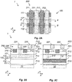
- FIG 2A With reference to figure 2A there is shown a schematic top-view of a multi-level interconnect structure 1 wherein both the first interconnection level 100 and the second interconnection level 200 are split into two sub-levels 110, 120 and 210, 220 respectively.
- Figure 2B shows the interconnect structure 1 along the plane of section AA' indicated in Figure 2A.
- Figure 2C shows the interconnect structure 1 along the plane of section BB' indicated in Figure 2A .
- the first interconnection level 100 comprises a first sub-level 110 and a second sub-level 120.
- the first sub-level 110 includes a set of conductive lines 111, 112 arranged in a first common horizontal plane (indicated by P11 in figure 2B and 2C ) of the first interconnection level 100.
- the set of lines 111, 112 are mutually parallel and extend in parallel to the first direction X.
- the second sub-level 120 is arranged directly on the first sub-level 110 of the first interconnection level 100.
- the second sub-level 120 includes a set of conductive lines 121, 122 arranged in a second common horizontal plane (indicated by P12 in figures 2B and 2C ) of the first interconnection level 100.
- the set of lines 121, 122 are mutually parallel and extend in parallel to the first direction X.
- the set of lines 111, 112 of the first sub-level 110 and the set of lines 121, 122 of the second sub-level 120 are horizontally displaced in relation to each other, along the second horizontal direction Y.
- the interleaved and nonoverlapping arrangement of the two sets of lines 111, 112 and 121, 122 may be seen in figure 2B and 2C .
- the first interconnection level 100 extends between the horizontal planes P10 and P12.
- the first sub-level 110 of the first interconnection level 100 extends between the horizontal planes P10 and P11.
- the second sub-level 120 of the first interconnection level 100 extends between the horizontal planes P11 and P12.
- the plane P11 coincides with the top-most surface of the set of conductive lines 111, 112 of the first sub-level 110.
- P11 represents an interface between the first sub-level 110 and the second sub-level 120.
- the plane P12 coincides with the top-most surface of the set of conductive lines 121, 122 of the second sub-level 120.
- the set of conductive lines 111, 112 are embedded in a dielectric layer 101 of the first sub-level 110 of the first interconnection level 100.
- the set of conductive lines 121, 122 are embedded in a dielectric layer 102 of the second sub-level 210 of the first interconnection level 100.
- the interconnect structure 1 includes a via 310 for interconnecting a line 112 of the set of lines 111, 112 of the first sub-level 110 of the first interconnection level 100 and a line 211 of the set of lines 211, 212 of the first sub-level 210 of the second interconnection level 200.
- the via 310 extends through the second sub-level 120 of the first interconnection level 100 and past the set of lines 121, 122 of the second sub-level 120 in a space between the lines 121, 222. Thus the via 310 is horizontally spaced apart from the lines 121, 122.
- the via 310 accordingly provides a direct electrical interconnection between a line 112 of the first sub-level 110 of the first interconnection level 100 and a line 211 of the first sub-level 210 of the second interconnection level 200 without any intermediate electrical connection with lines of the second sub-level 120. Accordingly, the via 310 is electrically insulated from the set of lines 121, 122. Although not shown in the figures, a corresponding via may be formed to interconnect the line 212 of the first sub-level 210 of the second interconnection level 200 and the line 111 of the first sub-level 110 of the first interconnection level 100.
- the interconnect structure 1 includes a via 320 corresponding to the via 320 shown in Figure 1B .
- the via 320 interconnects a line 121 of the set of lines 121, 122 of the second sub-level 120 of the first interconnection level 100 and a line 221 of the set of lines 221, 222 of the second sub-level 220 of the second interconnection level 200.
- the via 320 extends through the first sub-level 210 of the second interconnection level 200.
- a corresponding via may be formed to interconnect the line 222 of the second sub-level 220 of the second interconnection level 200 and the line 122 of the second sub-level 120 of the first interconnection level 100.
- FIG. 1 A method for forming an interconnection structure 1 as shown in figures 2A-C will now be described with reference to figures 3A-C through 19A-C .
- a sub-set of the following method steps may be performed to form an interconnection structure 1 as shown in figures 1A-B .
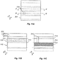
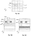
- partial-view A corresponds to the top-view shown in figure 2A
- partial-view B corresponds to the section along the plane AA'
- partial-view C corresponds to the section along the plane BB'.
- a dielectric layer 101 has been formed on the substrate 10.
- a mask layer 402 has been formed on the dielectric layer 101 and patterned to include trenches exposing the dielectric layer 101.
- the mask layer 402 may be patterned using single or multi-patterning techniques.
- the mask layer 402 may be a hard mask layer, for instance of a hard mask material such as titanium nitride, titanium oxide, hafnium oxide, zirconium oxide or a ruthenium or aluminum alloy, deposited by any suitable deposition method such as atomic layer deposition (ALD), chemical vapor deposition (CVD) or physical vapor deposition (PVD).
- the mask layer 402 may also be a layer of a-C, a-Si, spin-on-carbon (SOC), SiCN or even a photoresist.
- the trenches in the mask layer 402 have been transferred into the dielectric layer 101 by etching while using the mask layer 402 as an etch mask.
- Trenches for accommodating a set of lines of a first sub-level 110 of a first interconnection level 100 have thereby been formed in the dielectric layer 101.
- the pattern transfer may be performed by an anisotropic etch process.
- the etch process may be a plasma-based etching process.
- the etch process may be a reactive ion etching (RIE) process.
- RIE reactive ion etching
- F-based plasmas may be used for selectively etching a silicon oxide-based dielectric layer 101 with respect to a hard mask layer.
- the trenches in the dielectric layer 101 have been filled with a conductive line material, to form the set of lines 111, 112 of the first sub-level 110 of the first interconnection level 100.
- the conductive line material may for instance be Al, Cu or W.
- the trenches may be filled using an electro-plating process, or a deposition process such as CVD or ALD. Any conductive material overfilling the trenches may be removed by etch back and/or chemical mechanical polishing (CMP).
- a dielectric layer 102 has been formed on the first sub-level 110.
- a mask layer 404 has been formed on the dielectric layer 102 and patterned to include trenches exposing the dielectric layer 102.
- the mask layer 404 may be formed and patterned using any of the materials and techniques discussed in connection with the mask layer 402.
- the trenches in the mask layer 404 have been transferred into the dielectric layer 102 by etching while using the mask layer 404 as an etch mask. Trenches for accommodating a set of lines of a second sub-level 120 of the first interconnection level 100 have thereby been formed in the dielectric layer 102.
- the dielectric layer 102 may be etched using any of the etching processes discussed in connection with the patterning of the dielectric layer 101.
- the trenches in the dielectric layer 102 have subsequently been filled with a conductive line material, to form the set of lines 121, 122 of the second sub-level 120 of the first interconnection level 100.
- the conductive line material may be any of the materials discussed in connection with the filling of the trenches in the dielectric layer 101.
- the positions of the set of lines 111, 112 of the first sub-level 110 are indicated by dashed lines.
- a dielectric layer 2010 has been formed to cover the second sub-level 120 of the first interconnection level 100.
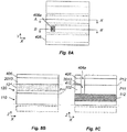
- a mask layer 406 has been formed to cover the dielectric layer 2010.
- the mask layer 406 may for instance be a hard mask layer of any of the afore-mentioned hard mask materials.
- a photo resist layer 408 has been formed on the mask layer 406 and patterned to include an opening 408a.
- the opening 408a defines a position of a via hole, to be transferred into the below layers.
- the opening 408a has been transferred into the mask layer 406 to form an opening 406a in the mask layer 406.
- the opening 406a has subsequently been further transferred into the dielectric layer 2010 and the dielectric layer 102 to form a via hole 412 exposing an upper surface of the line 112 of the first sub-level 110 of the first interconnection level 100.
- the photo resist layer 408 may as shown be consumed.
- the via hole 412 may be formed using an anisotropic etching process, such as a RIE-process.
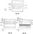
- the via hole 412 has been filled with a conductive via material.
- the via hole 412 may be filled by depositing the conductive via material in the via hole 412 by an electro-less deposition (ELD) process.
- ELD electro-less deposition
- Co, Ru or Ni may be deposited using ELD.
- An ELD process may result in a bottom-up growth of the conductive via material from the exposed surface of the line 112.
- An intermediate via structure 310a, protruding from the via hole 412 has accordingly been formed.
- the via hole 412 may be filled by depositing a conductive via material by CVD and removing material deposited outside the via hole 412 by CMP.
- the via hole 412 need not be filled completely with the conductive via material but a partial filling is also possible provided the via hole 412 is filled to a level matching at least an intended final via height.
- a dielectric liner may be formed on the sidewalls in the via hole 412 (not shown in the figures).
- the liner may for instance be formed by SiOx, SiN, SiCN or SiCO.
- the liner may be deposited as a conformal layer, for instance by ALD.
- the structure has been planarized wherein the protruding portion of the intermediate via structure 310a has been removed.
- the planarization may include etch back and/or CMP.
- the planarization may further result in the removal of the mask layer 406 and removal of portions of the liner (if deposited) outside the via hole 412.
- the planarization may also result in a thickness reduction of the dielectric layer 2010.
- the remaining part of the intermediate via structure 310a forms the final via 310. If the via hole 412 only has been partially filled with the conductive via material, the thickness of the dielectric layer 2010 may be reduced until an upper surface of the dielectric layer 2010 is coplanar with an upper surface of the via structure 310.
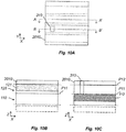
- an additional dielectric layer 2011 has been formed to cover the dielectric layer 2010.
- the additional dielectric layer 2011 may include a silicon dioxide layer or some other low- ⁇ material layer.
- the dielectric layer 2011 may include a protection layer of for instance SiCN formed below the low- ⁇ material layer.
- the layers 2010 and 2011 form part of a compound dielectric layer 201 of a first sub-level 210 of a second interconnection level 200.
- a mask layer 414 has been formed on the dielectric layer 201 of the first sub-level 210 of a second interconnection level 200 and patterned to include trenches exposing the dielectric layer 201.
- the mask layer 414 may be formed and patterned using any of the materials and techniques discussed in connection with the mask layer 402.
- Fig. 12A the positions of the set of lines 111, 112 of the first sub-level 110, the set of lines 121, 122 of the second sub-level 120 as well as the position of the via 310 are indicated by dashed lines.
- the trenches in the mask layer 414 have been transferred into the dielectric layer 201 by etching while using the mask layer 414 as an etch mask. Trenches for accommodating a set of lines of a first sub-level 210 of a second interconnection level 200 have thereby been formed in the dielectric layer 201.
- the dielectric layer 201 may be etched using any of the etching processes discussed in connection with the patterning of the dielectric layer 101 of the first sub-level 110 of the first interconnection level 100.
- the trenches extend through the dielectric layer 2011 and into the dielectric layer 2010.
- the set of trenches are formed such that one of the trenches thereof (i.e. the trench for accommodating the line 211) is aligned along the vertical direction with the via 310.
- a top portion of the via 310 may accordingly protrude from a bottom of said trench.
- the trenches may be formed to extend only through the dielectric layer 2011 such that an upper surface of the top portion of the via 310 is exposed at a bottom of the trench.
- the trenches in the dielectric layer 201 have been filled with a conductive line material, to form the set of lines 211, 212 of the first sub-level 210 of the second interconnection level 200.
- the conductive line material may be any of the materials discussed in connection with the filling of the trenches in the dielectric layer 101.
- the line 211 is hence formed on the top portion of the via 310.
- a dielectric layer 2020 has been formed to cover the first sub-level 210 of the second interconnection level 200.
- a mask layer 416 has been formed to cover the dielectric layer 2020.
- the mask layer 416 may for instance be a hard mask layer of any of the afore-mentioned hard mask materials.
- a photo resist layer 417 has been formed on the mask layer 416 and patterned to include an opening 417a.
- the opening 417a defines a position of a via hole, to be transferred into the below layers.
- the opening 417a has been transferred into the mask layer 416 to form an opening 416a in the mask layer 416.
- the opening 416a has subsequently been further transferred into the dielectric layer 2020 and the dielectric layer 201 of a first sub-level 210 of a second interconnection level 200 to form a via hole 418 exposing an upper surface of the line 121 of the second sub-level 120 of the first interconnection level 100.
- the photo resist layer 417 may as shown be consumed.
- the via hole 418 may be formed using any of the etching processes discussed in connection with the via hole 412.
- the via hole 418 has been filled with a conductive via material.
- the via hole 418 may be filled by depositing the conductive via material in the via hole 418 in a same manner as the via hole 412, as disclosed in connection with figures 9A-C .
- An intermediate via structure 320a, protruding from the via hole 418 has accordingly been formed.
- a dielectric liner may be formed also in the via hole 418 prior to the filling thereof.
- the structure has been planarized wherein the protruding portion of the intermediate via structure 320a has been removed.
- the planarization may include etch back and/or CMP.
- the planarization may further result in the removal of the mask layer 416 and removal of portions of the liner (if deposited) outside the via hole 418.
- the planarization may also result in a thickness reduction of the dielectric layer 2020.
- the remaining part of the intermediate via structure 320a forms the final via 320.
- the above method steps may be repeated to form further interconnection levels such as third and fourth interconnection levels above the second interconnection level 200.
- further interconnection levels such as third and fourth interconnection levels above the second interconnection level 200.
- the figures only illustrate a first and a second interconnection level 100, 200 it should be noted that the multi-level interconnect structure 1 may include further interconnection levels arranged below the first interconnection level 100.
- the further lower interconnection levels may include non-split tight pitch interconnection levels and/or interconnection levels split into two sub-levels.
Landscapes
- Design And Manufacture Of Integrated Circuits (AREA)
- Internal Circuitry In Semiconductor Integrated Circuit Devices (AREA)
Abstract
forming a first interconnection level including a set of conductive lines arranged in a first common horizontal plane of the first interconnection level and extending parallel to a first direction,
forming a second interconnection level, wherein forming the second interconnection level comprises:
forming, on the first interconnection level, a first sub-level of the second interconnection level, the first sub-level including a set of conductive lines arranged in a first common horizontal plane of the second interconnection level and extending parallel to a second direction transverse to the first direction, and
forming, on the first sub-level of the second interconnection level, a second sub-level of the second interconnection level, the second sub-level including a set of conductive lines arranged in a second common horizontal plane of the second interconnection level and extending parallel to the second direction,
wherein the first and the second sub-levels of the second interconnection level are formed as consecutive sub-levels and wherein said set of lines of the first sub-level of the second interconnection level and said set of lines of the second sub-level of the second interconnection level are horizontally displaced in relation to each other, and
forming a vertical via for interconnecting a line of said set of lines of the first interconnection level and a line of said set of lines of the second sub-level of the second interconnection level, wherein the via extends past said set of lines of the first sub-level of the second interconnection level in a space between a pair of adjacent lines of said set of lines of the first sub-level of the second interconnection level.
Description
- The present inventive concept relates to a method for forming a multi-level interconnect structure for a semiconductor device and a multi-level interconnect structure for a semiconductor device.
- To provide dense semiconductor integrated circuits, modern circuit design typically includes multi-level interconnect structures. A multi-level interconnect structure may include a number of vertically stacked interconnection levels arranged in a dielectric layer. Adjacent interconnection levels may be interconnected by vertically extending connections known as vias.
- An interconnection level may be formed by forming a pattern of conductive lines in the dielectric layer. A mask layer arranged on the dielectric layer may be patterned using lithographic techniques and etching. The pattern of the mask layer may subsequently be transferred into the dielectric layer by etching. A single patterning technique involving a single step of litho-etch may be used. Multiple patterning techniques like (litho-etch)x, or pitch splitting techniques such as self-aligned double patterning (SADP) or quadruple patterning (SAQP) may also be used. Multi patterning techniques enables further down-scaling of the pitch of the line patterns (i.e. a reduction of the line widths and line spacing) to sub-lithographic dimensions.
- Although dense lines patterns, in combination with modern semiconductor device fabrication, allow increasingly advanced, compact and power efficient integrated circuits, the reduced pitches of the interconnection levels may cause an increased resistance of the interconnect structure. This may have a negative impact on overall power efficiency and performance of the circuit.
- An objective of the present inventive concept is to address this issue. Further and/or alternatives objectives may be understood from the following.
- According to a first aspect of the present inventive concept there is provided a method for forming a multi-level interconnect structure for a semiconductor device, the method comprising:
- forming a first interconnection level including a set of conductive lines arranged in a first common horizontal plane of the first interconnection level and extending parallel to a first direction,
- forming a second interconnection level, wherein forming the second interconnection level comprises:
- forming, on the first interconnection level, a first sub-level of the second interconnection level, the first sub-level including a set of conductive lines arranged in a first common horizontal plane of the second interconnection level and extending parallel to a second direction transverse to the first direction, and
- forming, on the first sub-level of the second interconnection level, a second sub-level of the second interconnection level, the second sub-level including a set of conductive lines arranged in a second common horizontal plane of the second interconnection level and extending parallel to the second direction,
- wherein the first and the second sub-levels of the second interconnection level are formed as consecutive sub-levels and wherein said set of lines of the first sub-level of the second interconnection level and said set of lines of the second sub-level of the second interconnection level are horizontally displaced in relation to each other, and
- forming a vertical via for interconnecting a line of said set of lines of the first interconnection level and a line of said set of lines of the second sub-level of the second interconnection level, wherein the via extends past said set of lines of the first sub-level of the second interconnection level in a space between a pair of adjacent lines of said set of lines of the first sub-level of the second interconnection level.
- According to a second aspect of the present inventive concept there is provided a method for forming a multi-level interconnect structure for a semiconductor device, the method comprising:
- forming a first interconnection level, wherein forming the first interconnection level comprises:
- forming a first sub-level of the first interconnection level, the first sub-level including a set of conductive lines arranged in a first common horizontal plane of the first interconnection level and extending parallel to a first direction, and
- forming, on the first sub-level of the first interconnection level, a second sub-level of the first interconnection level, the second sub-level including a set of conductive lines arranged in a second common horizontal plane of the first interconnection level and extending parallel to the first direction,
- wherein the first and the second sub-levels of the first interconnection level are formed as consecutive sub-levels and wherein said set of lines of the first sub-level of the first interconnection level and said set of lines of the second sub-level of the first interconnection level are horizontally displaced in relation to each other,
- forming, on the second sub-level of the first interconnection level, a second interconnection level including a set of conductive lines arranged in a first common horizontal plane of the second interconnection level and extending parallel to a second direction transverse to the first direction, and
- forming a vertical via for interconnecting a line of said set of lines of the first sub-level of the first interconnection level and a line of said set of lines of the second interconnection level, wherein the via extends past said set of lines of the second sub-level of the first interconnection level in a space between a pair of adjacent lines of said set of lines of the second sub-level of the first interconnection level.
- According to a third aspect of the present inventive concept there is provided a multi-level interconnect structure for a semiconductor device, comprising:
- a first interconnection level including a set of conductive lines arranged in a first common horizontal plane of the first interconnection level and extending parallel to a first direction,
- a second interconnection level comprising:
- a first sub-level arranged on the first interconnection level, the first sub-level including a set of conductive lines arranged in a first common horizontal plane of the second interconnection level and extending parallel to a second direction transverse to the first direction, and
- a second sub-level arranged on the first sub-level of the second interconnection level, the second sub-level including a set of conductive lines arranged in a second common horizontal plane of the second interconnection level and extending parallel to the second direction,
- wherein the first and the second sub-levels of the second interconnection level are arranged as consecutive sub-levels and wherein said set of lines of the first sub-level of the second interconnection level and said set of lines of the second sub-level of the second interconnection level are horizontally displaced in relation to each other, and
- a vertical via for interconnecting a line of said set of lines of the first interconnection level and a line of said set of lines of the second sub-level of the second interconnection level, wherein the via extends past said set of lines of the first sub-level of the second interconnection level in a space between a pair of adjacent lines of said set of lines of the first sub-level of the second interconnection level.
- According to a fourth aspect of the present inventive concept there is provided a multi-level interconnect structure for a semiconductor device, comprising:
- a first interconnection level comprising:
- a first sub-level, the first sub-level including a set of conductive lines arranged in a first common horizontal plane of the first interconnection level and extending parallel to a first direction, and
- a second sub-level arranged on the first sub-level of the first interconnection level, the second sub-level including a set of conductive lines arranged in a second common horizontal plane of the first interconnection level and extending parallel to the first direction,
- wherein the first and the second sub-levels of the first interconnection level are arranged as consecutive sub-levels and wherein said set of lines of the first sub-level of the first interconnection level and said set of lines of the second sub-level of the first interconnection level are horizontally displaced in relation to each other,
- a second interconnection level arranged on the second sub-level of the first interconnection level, the second interconnection level including a set of conductive lines arranged in a first common horizontal plane of the second interconnection level and extending parallel to a second direction transverse to the first direction, and
- a vertical via for interconnecting a line of said set of lines of the first sub-level of the first interconnection level and a line of said set of lines of the second interconnection level, wherein the via extends past said set of lines of the second sub-level of the first interconnection level in a space between a pair of adjacent lines of said set of lines of the second sub-level of the first interconnection level.
- The present inventive concept is based on the technical insight that a conventional single interconnection level may be split into, or replaced with, two sub-interconnection levels including sets of parallel lines. This split design allows the pitches of the lines of the sub-levels to be relaxed compared to a conventional single interconnection level as the lines may be distributed between two levels. By "pitch" is hereby meant a line width and a line spacing within a horizontal plane.
- Merely arranging an interconnection level to include two sub-levels per se could cause a reduced overall routing density of the interconnection structure. The present inventive concept however enables the routing density to be maintained by a vertical via providing a direct interconnection between a pair of lines of two interconnection levels (at least one being a sub-level of a first or second interconnection level).
- The interconnection provided by the via may be referred to as a "direct" vertical interconnection: In accordance with the first and third aspect, a line of said set of lines of the first interconnection level and a line of said set of lines of the second sub-level of the second interconnection level may be interconnected by the via while the via (electrically) bypasses the first sub-level of the second interconnection level. In accordance with the second and fourth aspect, a line of said set of lines of the first sub-level of the first interconnection level and a line of said set of lines of the second interconnection level may be interconnected by the via while the via (electrically) bypasses the second sub-level of the first interconnection level.
- Said vertical vias may accordingly be referred to as "multilayer vias" or "supervias" since it has a physical extension exceeding the separation between two adjacent (sub-)levels.
- By the set of lines of the two sub-levels being horizontally displaced in relation to each other the set of lines of the two sub-levels may be arranged in an interleaved manner. This facilitates forming of a vertical via to extend through a sub-level without interfering with the lines of sub-level. That is, a via may be formed to extend in a vertical straight-line path from a line of one sub-level through a space or gap formed between a pair of consecutive lines of the other the sub-level and to a connecting line.
- A further merit of the present inventive concept is that introduction of sub-levels need not result in any significant increased of the complexity of the process or the number of litho-etch steps. Since the sub-levels allows forming of the lines of the sub-levels at relaxed pitches, there may be less need to use multi-patterning techniques forming the lines of the sub-levels. For instance, even single patterning techniques may be used.
- As used herein, the term "horizontal" direction or "horizontal" plane denotes a direction or plane being parallel to a main plane of extension of any of the interconnection levels. The multi-layer interconnection structure may be supported by a substrate wherein the term "horizontal" direction or "horizontal" plane equivalently may be understood as a direction parallel to a main plane of extension of the substrate.
- As used herein, the term "vertical" direction or "vertical" plane denotes a direction or plane being perpendicular to a horizontal direction or horizontal plane. I.e. the term "vertical" direction or "vertical plane" denotes a direction or plane being perpendicular to a main plane of extension of any of the interconnection levels, or of a substrate supporting the interconnection structure.
- Accordingly, the terms "above" and "below" refer to directions along the vertical direction and opposite to the vertical direction, respectively.
- By "interconnection level" is hereby meant a level, or a tier, of an interconnection structure of the device. An interconnection level may also be referred to as a metallization or a routing level.
- Each interconnection level includes at least one set of parallel conductive lines arranged in a common horizontal plane. The set of conductive lines of each interconnection level may be arranged to provide a horizontal routing of (electrical) signals, i.e. a routing within the common horizontal plane of the set of conductive lines.
- Each set of conductive lines may be regularly spaced lines. The material lines may be spaced apart such that longitudinal gaps are formed between the lines. The gaps may present a regular width and spacing. Advantageously, the lines may, at least along a portion thereof, extend in a straight line and present a uniform width or substantially uniform width. This applies accordingly to the gaps between the lines.
- Each set of lines may be arranged in a dielectric layer of the respective interconnection (sub-)level. A dielectric layer may be formed as a single material layer, or as a compound layer including a stack of sub-layers formed of different materials.
- By "via" as used herein is meant a conductive structure extending in a vertical direction between lines of different interconnection levels. The interconnect structure may, in addition to the afore-mentioned multi-level vias, also include vertical "single-level" vias. By "single-level" via is hereby meant a via for interconnecting lines of two consecutive interconnection (sub-)levels. Vias of the interconnect structure may hence be arranged to provide a vertical routing of (electrical) signals, i.e. a routing perpendicular to the set of conductive lines.
- According to one embodiment of the first aspect, forming the via comprises:
- subsequent to forming the first sub-level of the second interconnection level and prior to forming the set of lines of the second sub-level of the second interconnection level, covering the first sub-level of the second interconnection level with a dielectric layer,
- forming a via hole extending through said dielectric layer and the first sub-level of the second interconnection level to said line of said set of lines of the first interconnection level, and
- filling the via hole with a conductive via material.
- Forming the via prior to forming the set of lines of the second sub-level of the second interconnection level facilitates the via formation since the set of lines of the second sub-level of the second interconnection level may then not interfere with the via hole formation and the filling of the via hole.
- The set of lines of the second sub-level of the second interconnection level may subsequently be formed such that said line of said set of lines of the second sub-level of the second interconnection level is formed on a top portion of the via.
- More specifically, forming the second sub-level of the second interconnection level may comprise:
- covering said dielectric layer with an additional dielectric layer,
- forming a set of trenches for accommodating said set of lines of the second sub-level of the second interconnection level, wherein said set of trenches extends through said additional dielectric layer, and wherein said set of trenches are formed such that the top portion of the via is exposed at a bottom of a trench of said set of trenches, and
- filling said set of trenches with a conductive line material to form said set of lines of the second sub-level.
- Preferably, forming the second sub-level of the second interconnection level may comprise:
- covering said dielectric layer with an additional dielectric layer,
- forming a set of trenches for accommodating said set of lines of the second sub-level of the second interconnection level, wherein said set of trenches extends through said additional dielectric layer and into said dielectric layer, wherein said set of trenches are formed such that the top portion of the via protrudes from a bottom of a trench of said set of trenches, and
- filling said set of trenches with a conductive line material to form said set of lines of the second sub-level.
- Thereby (the conductive line material forming) said line of the second sub-level of the second interconnection level may enclose the top portion of the via. This enables a good galvanic contact between the via and the line.
- The above-mentioned embodiments and options of the first aspect, may apply corresponding to the second aspect and hence provide corresponding advantages.
- Accordingly, according to one embodiment of the second aspect, forming the via comprises:
- subsequent to forming the second sub-level of the first interconnection level and prior to forming the set of lines of the second interconnection level, covering the second sub-level of the first interconnection level with a dielectric layer,
- forming a via hole extending through said dielectric layer and the second sub-level of the first interconnection level to said line of the first sub-level of the first interconnection level, and
- filling the via hole with a conductive via material.
- The set of lines of the second interconnection level may subsequently be formed such that said line of said set of lines of the second interconnection level is formed on a top portion of the via.
- More specifically, forming the second interconnection level may comprise:
- covering said dielectric layer with an additional dielectric layer of the second interconnection level,
- forming a set of trenches for accommodating said set of lines of the second interconnection level, wherein said set of trenches extends through said additional dielectric layer, and wherein said set of trenches are formed such that the top portion of the via is exposed at a bottom of a trench of said set of trenches, and
- filling said set of trenches with a conductive line material to form said set of lines of the second sub-level.
- Preferably, forming the second interconnection level may comprise:
- covering said dielectric layer with an additional dielectric layer of the second interconnection level,
- forming a set of trenches for accommodating said set of lines of the second interconnection level, wherein said set of trenches extends through said additional dielectric layer and into said dielectric layer, wherein said set of trenches are formed such that the top portion of the via protrudes from a bottom of a trench of said set of trenches, and
- filling said set of trenches with a conductive line material to form said set of lines of the second sub-level.
- Thereby (the conductive line material forming) said line of the second interconnection level may enclose the top portion of the via.
- According to embodiments of the first and the second aspect, filling the via hole includes depositing the conductive via material in the via hole by an electro-less deposition process. This enables selective deposition of the conductive via material in the via hole. Reliable filling of the via hole may hence be provided even in case of via holes with comparably high aspect ratios.
- The via hole may be filled completely with the conductive via material. The via hole may be over-filled wherein excess conductive via material may be removed subsequently. The via hole may be partially filled wherein a thickness of the dielectric layer (through which the via hole extends) may be reduced such that an upper surface of the dielectric layer becomes flush with an upper surface of the via.
- According to embodiments of the first and the second aspect, the method may further comprise forming a dielectric liner in the via hole prior to filling the via hole with the conductive via material. A dielectric liner may provide a double-function of acting as a diffusion barrier for the conductive via material and enabling an improved time-dependent dielectric breakdown performance.
- As may be understood from the above, the first and second aspect on the one hand, and the third and fourth aspect on the other hand, represent alternative methods for forming multi-level interconnect structures and alternative multi-level interconnect structures, consistent with the general inventive concept.
- According to advantageous embodiments, both the first and the second interconnection levels may be formed or arranged to include a first and a second sub-level.
- Accordingly, there is provided a method method for forming a multi-level interconnect structure, the method comprising:
- forming a first interconnection level , wherein forming the first interconnection level comprises:
- forming a first sub-level of the first interconnection level , the first sub-level including a set of conductive lines arranged in a first common horizontal plane of the first interconnection level and extending parallel to a first direction, and
- forming, on the first sub-level of the first interconnection level, a second sub-level of the first interconnection level , the second sub-level including a set of conductive lines arranged in a second common horizontal plane of the first interconnection level and extending parallel to the first direction,
- wherein the first and the second sub-levels of the first interconnection level are formed as consecutive sub-levels and wherein said set of lines of the first sub-level of the first interconnection level and said set of lines of the second sub-level of the first interconnection level are horizontally displaced in relation to each other, and
- forming a second interconnection level, wherein forming the second interconnection level comprises:
- forming, on the first interconnection level, a first sub-level of the second interconnection level , the first sub-level including a set of conductive lines arranged in a first common horizontal plane of the second interconnection level and extending parallel to a second direction transverse to the first direction, and
- forming, on the first sub-level of the second interconnection level, a second sub-level of the second interconnection level, the second sub-level including a set of conductive lines arranged in a second common horizontal plane of the second interconnection level and extending parallel to the second direction,
- wherein the first and the second sub-levels of the second interconnection level are formed as consecutive sub-levels and wherein said set of lines of the first sub-level of the second interconnection level and said set of lines of the second sub-level of the second interconnection level are horizontally displaced in relation to each other.
- The method may further comprise:
- forming a (first) vertical via for interconnecting a line of said set of lines of the first sub-level of the first interconnection level and a line of said set of lines of the first sub-level of the second interconnection level , wherein the via extends past said set of lines of the second sub-level of the first interconnection level in a space between a pair of adjacent lines of said set of lines of the second sub-level of the first interconnection level , and/or
- forming a (second) vertical via for interconnecting a line of said set of lines of the second sub-level of the the first interconnection level and a line of said set of lines of the second sub-level of the second interconnection level , wherein the via extends past said set of lines of the first sub-level of the second interconnection level in a space between a pair of adjacent lines of said set of lines of the first sub-level of the second interconnection level .
- There is further provided a corresponding multi-level interconnect structure comprising:
- a first interconnection level comprising:
- a first sub-level, the first sub-level including a set of conductive lines arranged in a first common horizontal plane of the first interconnection level and extending parallel to a first direction, and
- a second sub-level arranged on the first sub-level of the first interconnection level, the second sub-level including a set of conductive lines arranged in a second common horizontal plane of the first interconnection level and extending parallel to the first direction,
- wherein the first and the second sub-levels of the first interconnection level are arranged as consecutive sub-levels and wherein said set of lines of the first sub-level of the first interconnection level and said set of lines of the second sub-level of the first interconnection level are horizontally displaced in relation to each other, and
- a second interconnection level comprising:
- a first sub-level arranged on the first interconnection level, the first sub-level including a set of conductive lines arranged in a first common horizontal plane of the second interconnection level and extending parallel to a second direction transverse to the first direction, and
- a second sub-level arranged on the first sub-level of the second interconnection level, the second sub-level including a set of conductive lines arranged in a second common horizontal plane of the second interconnection level and extending parallel to the second direction,
- wherein the first and the second sub-levels of the second interconnection level are arranged as consecutive sub-levels and wherein said set of lines of the first sub-level of the second interconnection level and said set of lines of the second sub-level of the second interconnection level are horizontally displaced in relation to each other.
- The multi-level interconnect structure may further comprise:
- a (first) vertical via for interconnecting a line of said set of lines of the first sub-level of the first interconnection level and a line of said set of lines of the first sub-level of the second interconnection level, wherein the via extends past said set of lines of the second sub-level of the first interconnection level in a space between a pair of adjacent lines of said set of lines of the second sub-level of the first interconnection level, and/or
- a (second) vertical via for interconnecting a line of said set of lines of the second sub-level of the the first interconnection level and a line of said set of lines of the second sub-level of the second interconnection level , wherein the via extends past said set of lines of the first sub-level of the second interconnection level in a space between a pair of adjacent lines of said set of lines of the first sub-level of the second interconnection level.
- The merits of the split level design and multi-level via may hence be provided in both the first and the second interconnection level.
- According to an alternative embodiment of any of the first and third aspects, a line width of the set of lines of the first and second sub-levels of the second interconnection level may be greater than a line width of the set of lines of the first interconnection level .
- Additionally, a horizontal spacing of the set of lines of the first sub-level of the second interconnection level and a horizontal spacing of the set of lines of the second sub-level of the second interconnection level may be greater than a horizontal spacing of the set of lines of the first interconnection level .
- According to an alternative embodiment of any of the second and fourth aspects, a line width of the set of lines of the first and second sub-levels of the first interconnection level may be greater than a line width of the set of lines of the second interconnection level .
- Additionally, a horizontal spacing of the set of lines of the first sub-level of the first interconnection level and a horizontal spacing of the set of lines of the second sub-level of the first interconnection level may be greater than a horizontal spacing of the set of lines of the second interconnection level
- According to the above, a multi-level interconnect structure including a combination of a non-split tight pitch interconnection levels and split-level interconnection levels may hence be provided. A line width and/or line spacing of the lines of the sub-levels is preferably twice that of the non-split level.
- According to a fifth aspect there is provided a method for forming an integrated circuit comprising:
- forming on a substrate a multi-level interconnect structure in accordance with the first and/or second aspect.
- According to a sixth aspect there is provided an integrated circuit comprising:
- a substrate, and
- a multi-level interconnect structure in accordance with the third and/or fourth aspect.
- This aspect may generally convey the same or corresponding advantages as the former aspects to an integrated circuit.
- The above, as well as additional objects, features and advantages of the present inventive concept, will be better understood through the following illustrative and non-limiting detailed description, with reference to the appended drawings. In the drawings like reference numerals will be used for like elements unless stated otherwise.
-
Figures 1A-B are schematic illustrations of a multi-level interconnect structure. -
Figures 2A-C are schematic illustrations of an alternative multi-level interconnect structure. -
Figures 3A-C through 19A-C schematically illustrate a method for forming a multi-level interconnect structure. - With reference to
figure 1A there is shown a schematic top-view of amulti-level interconnect structure 1.Figure 1B shows theinterconnect structure 1 along the plane of section AA' indicated inFigure 1A . Infigures 1A and 1B , as well as the further figures, the indicated directions X, Y and Z consistently refer to a first horizontal direction, a second horizontal direction and a vertical direction, respectively. It should be noted that thestructure 1 may extend laterally or horizontally beyond the illustrated portions. It should further be noted that, owing to the schematic nature of the drawings, the relative dimensions of the various structures and layers are not drawn to scale. Rather, the dimensions have been adapted for illustrational clarity and to facilitate understanding of the following description. - The
interconnect structure 1 may as schematically indicated be arranged on asubstrate 10. Thesubstrate 10 may be a semiconductor wafer or substrate, for instance a Si substrate, a Ge substrate, a SiGe substrate, a SiC substrate, a SOI substrate, a GeOI substrate, a SiGeOI substrate to name a few examples. - The
substrate 10 may support an active device layer including active devices, for instance semiconductor devices such as transistors and other solid state devices. The active devices may have been formed using conventional front-end-of-line (FEOL) processing. Theinterconnect structure 1 together with thesubstrate 10 and the active devices may form part of an integrated circuit. - The
multi-level interconnect structure 1 comprises in a bottom-up direction afirst interconnection level 100 and asecond interconnection level 200. Thefirst interconnection level 100 and thesecond interconnection level 200 form consecutive levels of theinterconnect structure 1. - The
first interconnection level 100 includes a set of conductive lines 111-114 arranged in a first common horizontal plane (indicated by P11 infigure 1 B) of thefirst interconnection level 100. The set of lines 111-114 are mutually parallel and extend in parallel to the first direction X. Thefirst interconnection level 100 extends between the horizontal planes indicated by P10 and P11. P11 coincides with the top-most surface of the set ofconductive lines first interconnection level 100. P11 represents an interface between thefirst interconnection level 100 and thesecond interconnection level 200. Thefirst interconnection level 100 includes only a single co-planar set of conductive lines. Thefirst interconnection level 100 may hence be referred to as a single-level interconnection level or non-split interconnection level. Although the figures only show interconnection levels including sets of four conductive lines, each interconnection level may in practice include a much greater number of lines than four. - The
second interconnection level 200 includes two co-planar sets of conductive lines, the set oflines lines second interconnection level 200. Thesecond interconnection level 200 hence includes, or is split into, a first sub-level 210 including the set oflines consecutive sub-level 220 including the set oflines second interconnection level 200 may hence be referred to as a dual-level interconnection level or split interconnection level. - The
first sub-level 210 of thesecond interconnection level 200 is arranged directly on thefirst interconnection level 100. Thesecond sub-level 220 is arranged directly on thefirst sub-level 210 of thesecond interconnection level 200. - The
second interconnection level 200 extends between the horizontal planes P11 and P22. Thefirst sub-level 210 of thesecond interconnection level 200 extends between the horizontal planes P11 and P21. Thesecond sub-level 220 of thesecond interconnection level 200 extends between the horizontal planes P21 and P22. The plane P21 coincides with the top-most surface of the set ofconductive lines first sub-level 210. P21 represents an interface between thefirst sub-level 210 and thesecond sub-level 220. The plane P22 coincides with the top-most surface of the set ofconductive lines second sub-level 220. - The
first sub-level 210 includes a set ofconductive lines figure 1 B) of thesecond interconnection level 200. The set oflines - The
second sub-level 220 includes a set ofconductive lines figure 1 B) of thesecond interconnection level 200. The set oflines - The set of
lines first sub-level 210 and the set oflines second sub-level 220 are horizontally displaced in relation to each other, along the first horizontal direction X. The interleaved and nonoverlapping arrangement of the two sets oflines figure 1A and 1B . - As indicated in
Fig. 1A , the pitch of the set oflines first sub-level 210 is greater than the pitch of the set of lines 111-114 of thefirst interconnection level 100. Correspondingly, the pitch of the set oflines second sub-level 220 is greater than the pitch of the set of lines 111-114 of thefirst interconnection level 100. The increased pitch also allows an increased height or thickness of thelines - The set of conductive lines 111-114 of the
first interconnection level 100 and the set ofconductive lines - The set of conductive lines 111-114 are embedded in a
dielectric layer 101 of thefirst interconnection level 100. The set ofconductive lines dielectric layer 201 of thefirst sub-level 210 of thesecond interconnection level 200. Correspondingly, the set ofconductive lines dielectric layer 202 of thesecond sub-level 220 of thesecond interconnection level 200. Each of thedielectric layers - With reference to
figure 1B , theinterconnect structure 1 includes a vertical via 320 for interconnecting theline 112 of thefirst interconnection level 100 and theline 221 of thesecond sub-level 220 of thesecond interconnection level 200. The via 320 extends from theline 221 of thesecond sub-level 220, in the vertical direction Z, to theline 112 of thefirst interconnection level 100. The via 320 extends through thefirst sub-level 210 of thesecond interconnection level 200 and past the set oflines lines lines line 221 of thesecond sub-level 220 and aline 112 of thefirst interconnection level 100 without any intermediate electrical connection with lines of thefirst sub-level 210. Accordingly, the via 320 is electrically insulated from the set oflines - As shown, the
interconnect strucure 1 may further include a single-level via 305 for interconnecting aline 211 of thefirst sub-level 210 of thesecond interconnection level 200 with aline 112 of thefirst interconnection level 100. - Although in
figure 1A and 1B thesecond interconnection level 200 is arranged as a split interconnection level and thefirst interconnection level 100 is arranged as a non-split interconnection level, the opposite arrangement is also possible. Accordingly, thefirst interconnection level 100 may be arranged as a split interconnection level and thesecond interconnection level 200 may be arranged as a non-split interconnection level. In that case, the interconnect structure may include a vertical via for interconnecting a line of a set of lines of the first sub-level of thefirst interconnection level 100 and a line of a set of lines of thesecond interconnection level 200, wherein the via extends past a set of lines of the second sub-level of thefirst interconnection level 100. - With reference to
figure 2A there is shown a schematic top-view of amulti-level interconnect structure 1 wherein both thefirst interconnection level 100 and thesecond interconnection level 200 are split into twosub-levels Figure 2B shows theinterconnect structure 1 along the plane of section AA' indicated inFigure 2A. Figure 2C shows theinterconnect structure 1 along the plane of section BB' indicated inFigure 2A . - The description of the
second interconnection level 200 in connection withfigure 1A and 1B applies correspondingly to thesecond interconnection level 200 shown infigures 2A-C . - The
first interconnection level 100 comprises afirst sub-level 110 and asecond sub-level 120. Thefirst sub-level 110 includes a set ofconductive lines figure 2B and 2C ) of thefirst interconnection level 100. The set oflines second sub-level 120 is arranged directly on thefirst sub-level 110 of thefirst interconnection level 100. Thesecond sub-level 120 includes a set ofconductive lines figures 2B and 2C ) of thefirst interconnection level 100. The set oflines - The set of
lines first sub-level 110 and the set oflines second sub-level 120 are horizontally displaced in relation to each other, along the second horizontal direction Y. The interleaved and nonoverlapping arrangement of the two sets oflines figure 2B and 2C . - The
first interconnection level 100 extends between the horizontal planes P10 and P12. Thefirst sub-level 110 of thefirst interconnection level 100 extends between the horizontal planes P10 and P11. Thesecond sub-level 120 of thefirst interconnection level 100 extends between the horizontal planes P11 and P12. The plane P11 coincides with the top-most surface of the set ofconductive lines first sub-level 110. P11 represents an interface between thefirst sub-level 110 and thesecond sub-level 120. The plane P12 coincides with the top-most surface of the set ofconductive lines second sub-level 120. - The set of
conductive lines dielectric layer 101 of thefirst sub-level 110 of thefirst interconnection level 100. The set ofconductive lines dielectric layer 102 of thesecond sub-level 210 of thefirst interconnection level 100. - The
interconnect structure 1 includes a via 310 for interconnecting aline 112 of the set oflines first sub-level 110 of thefirst interconnection level 100 and aline 211 of the set oflines first sub-level 210 of thesecond interconnection level 200. The via 310 extends through thesecond sub-level 120 of thefirst interconnection level 100 and past the set oflines lines lines line 112 of thefirst sub-level 110 of thefirst interconnection level 100 and aline 211 of thefirst sub-level 210 of thesecond interconnection level 200 without any intermediate electrical connection with lines of thesecond sub-level 120. Accordingly, the via 310 is electrically insulated from the set oflines line 212 of thefirst sub-level 210 of thesecond interconnection level 200 and theline 111 of thefirst sub-level 110 of thefirst interconnection level 100. - The
interconnect structure 1 includes a via 320 corresponding to the via 320 shown inFigure 1B . The via 320 interconnects aline 121 of the set oflines second sub-level 120 of thefirst interconnection level 100 and aline 221 of the set oflines second sub-level 220 of thesecond interconnection level 200. The via 320 extends through thefirst sub-level 210 of thesecond interconnection level 200. Although not shown in the figures, a corresponding via may be formed to interconnect theline 222 of thesecond sub-level 220 of thesecond interconnection level 200 and theline 122 of thesecond sub-level 120 of thefirst interconnection level 100. - A method for forming an
interconnection structure 1 as shown infigures 2A-C will now be described with reference tofigures 3A-C through 19A-C . As may be understood, a sub-set of the following method steps may be performed to form aninterconnection structure 1 as shown infigures 1A-B . In the following, partial-view A corresponds to the top-view shown infigure 2A , partial-view B corresponds to the section along the plane AA' and partial-view C corresponds to the section along the plane BB'. - In
figures 3A-C , adielectric layer 101 has been formed on thesubstrate 10. Amask layer 402 has been formed on thedielectric layer 101 and patterned to include trenches exposing thedielectric layer 101. Themask layer 402 may be patterned using single or multi-patterning techniques. Themask layer 402 may be a hard mask layer, for instance of a hard mask material such as titanium nitride, titanium oxide, hafnium oxide, zirconium oxide or a ruthenium or aluminum alloy, deposited by any suitable deposition method such as atomic layer deposition (ALD), chemical vapor deposition (CVD) or physical vapor deposition (PVD). Themask layer 402 may also be a layer of a-C, a-Si, spin-on-carbon (SOC), SiCN or even a photoresist. - In
figures 4A-C the trenches in themask layer 402 have been transferred into thedielectric layer 101 by etching while using themask layer 402 as an etch mask. Trenches for accommodating a set of lines of afirst sub-level 110 of afirst interconnection level 100 have thereby been formed in thedielectric layer 101. The pattern transfer may be performed by an anisotropic etch process. The etch process may be a plasma-based etching process. The etch process may be a reactive ion etching (RIE) process. For instance, F-based plasmas may be used for selectively etching a silicon oxide-baseddielectric layer 101 with respect to a hard mask layer. - The trenches in the
dielectric layer 101 have been filled with a conductive line material, to form the set oflines first sub-level 110 of thefirst interconnection level 100. The conductive line material may for instance be Al, Cu or W. The trenches may be filled using an electro-plating process, or a deposition process such as CVD or ALD. Any conductive material overfilling the trenches may be removed by etch back and/or chemical mechanical polishing (CMP). - In
figures 5A-C adielectric layer 102 has been formed on thefirst sub-level 110. Amask layer 404 has been formed on thedielectric layer 102 and patterned to include trenches exposing thedielectric layer 102. Themask layer 404 may be formed and patterned using any of the materials and techniques discussed in connection with themask layer 402. - In
figures 6A-C the trenches in themask layer 404 have been transferred into thedielectric layer 102 by etching while using themask layer 404 as an etch mask. Trenches for accommodating a set of lines of asecond sub-level 120 of thefirst interconnection level 100 have thereby been formed in thedielectric layer 102. Thedielectric layer 102 may be etched using any of the etching processes discussed in connection with the patterning of thedielectric layer 101. The trenches in thedielectric layer 102 have subsequently been filled with a conductive line material, to form the set oflines second sub-level 120 of thefirst interconnection level 100. The conductive line material may be any of the materials discussed in connection with the filling of the trenches in thedielectric layer 101. InFig. 6A the positions of the set oflines first sub-level 110 are indicated by dashed lines. - In
figures 7A-C adielectric layer 2010 has been formed to cover thesecond sub-level 120 of thefirst interconnection level 100. Amask layer 406 has been formed to cover thedielectric layer 2010. Themask layer 406 may for instance be a hard mask layer of any of the afore-mentioned hard mask materials. A photo resistlayer 408 has been formed on themask layer 406 and patterned to include anopening 408a. Theopening 408a defines a position of a via hole, to be transferred into the below layers. - In
figures 8A-C theopening 408a has been transferred into themask layer 406 to form anopening 406a in themask layer 406. Theopening 406a has subsequently been further transferred into thedielectric layer 2010 and thedielectric layer 102 to form a viahole 412 exposing an upper surface of theline 112 of thefirst sub-level 110 of thefirst interconnection level 100. During the etching of the viahole 412 the photo resistlayer 408 may as shown be consumed. The viahole 412 may be formed using an anisotropic etching process, such as a RIE-process. - In
figures 9A-C , the viahole 412 has been filled with a conductive via material. The viahole 412 may be filled by depositing the conductive via material in the viahole 412 by an electro-less deposition (ELD) process. For instance, Co, Ru or Ni may be deposited using ELD. An ELD process may result in a bottom-up growth of the conductive via material from the exposed surface of theline 112. An intermediate viastructure 310a, protruding from the viahole 412 has accordingly been formed. As an alternative to ELD, the viahole 412 may be filled by depositing a conductive via material by CVD and removing material deposited outside the viahole 412 by CMP. The viahole 412 need not be filled completely with the conductive via material but a partial filling is also possible provided the viahole 412 is filled to a level matching at least an intended final via height. - Prior to filling the via
hole 412 with a conductive via material, a dielectric liner may be formed on the sidewalls in the via hole 412 (not shown in the figures). The liner may for instance be formed by SiOx, SiN, SiCN or SiCO. The liner may be deposited as a conformal layer, for instance by ALD. - In
figures 10A-C , the structure has been planarized wherein the protruding portion of the intermediate viastructure 310a has been removed. The planarization may include etch back and/or CMP. The planarization may further result in the removal of themask layer 406 and removal of portions of the liner (if deposited) outside the viahole 412. The planarization may also result in a thickness reduction of thedielectric layer 2010. The remaining part of the intermediate viastructure 310a forms the final via 310. If the viahole 412 only has been partially filled with the conductive via material, the thickness of thedielectric layer 2010 may be reduced until an upper surface of thedielectric layer 2010 is coplanar with an upper surface of the viastructure 310. - In
figures 11A-C anadditional dielectric layer 2011 has been formed to cover thedielectric layer 2010. Theadditional dielectric layer 2011 may include a silicon dioxide layer or some other low-κ material layer. To avoid direct contact between low-κ material layer and a top surface of the via 310, thedielectric layer 2011 may include a protection layer of for instance SiCN formed below the low-κ material layer. Thelayers compound dielectric layer 201 of afirst sub-level 210 of asecond interconnection level 200. - In
figures 12A-C amask layer 414 has been formed on thedielectric layer 201 of thefirst sub-level 210 of asecond interconnection level 200 and patterned to include trenches exposing thedielectric layer 201. Themask layer 414 may be formed and patterned using any of the materials and techniques discussed in connection with themask layer 402. InFig. 12A the positions of the set oflines first sub-level 110, the set oflines - In
figures 13A-C the trenches in themask layer 414 have been transferred into thedielectric layer 201 by etching while using themask layer 414 as an etch mask. Trenches for accommodating a set of lines of afirst sub-level 210 of asecond interconnection level 200 have thereby been formed in thedielectric layer 201. Thedielectric layer 201 may be etched using any of the etching processes discussed in connection with the patterning of thedielectric layer 101 of thefirst sub-level 110 of thefirst interconnection level 100. - The trenches extend through the
dielectric layer 2011 and into thedielectric layer 2010. The set of trenches are formed such that one of the trenches thereof (i.e. the trench for accommodating the line 211) is aligned along the vertical direction with the via 310. Following the trench formation, a top portion of the via 310 may accordingly protrude from a bottom of said trench. Alternatively, the trenches may be formed to extend only through thedielectric layer 2011 such that an upper surface of the top portion of thevia 310 is exposed at a bottom of the trench. - In
figures 13A-C , the trenches in thedielectric layer 201 have been filled with a conductive line material, to form the set oflines first sub-level 210 of thesecond interconnection level 200. The conductive line material may be any of the materials discussed in connection with the filling of the trenches in thedielectric layer 101. Theline 211 is hence formed on the top portion of thevia 310. - In
figures 14A-C adielectric layer 2020 has been formed to cover thefirst sub-level 210 of thesecond interconnection level 200. Amask layer 416 has been formed to cover thedielectric layer 2020. Themask layer 416 may for instance be a hard mask layer of any of the afore-mentioned hard mask materials. A photo resistlayer 417 has been formed on themask layer 416 and patterned to include anopening 417a. Theopening 417a defines a position of a via hole, to be transferred into the below layers. - In
figures 15A-C theopening 417a has been transferred into themask layer 416 to form anopening 416a in themask layer 416. Theopening 416a has subsequently been further transferred into thedielectric layer 2020 and thedielectric layer 201 of afirst sub-level 210 of asecond interconnection level 200 to form a viahole 418 exposing an upper surface of theline 121 of thesecond sub-level 120 of thefirst interconnection level 100. During the etching of the viahole 418 the photo resistlayer 417 may as shown be consumed. The viahole 418 may be formed using any of the etching processes discussed in connection with the viahole 412. - In
figures 16A-C , the viahole 418 has been filled with a conductive via material. The viahole 418 may be filled by depositing the conductive via material in the viahole 418 in a same manner as the viahole 412, as disclosed in connection withfigures 9A-C . An intermediate viastructure 320a, protruding from the viahole 418 has accordingly been formed. Analogous to the viahole 412, a dielectric liner may be formed also in the viahole 418 prior to the filling thereof. - In
figures 17A-C , the structure has been planarized wherein the protruding portion of the intermediate viastructure 320a has been removed. The planarization may include etch back and/or CMP. The planarization may further result in the removal of themask layer 416 and removal of portions of the liner (if deposited) outside the viahole 418. The planarization may also result in a thickness reduction of thedielectric layer 2020. The remaining part of the intermediate viastructure 320a forms the final via 320. - In
figures 18A-C and19A-C , process steps corresponding to those described in connection withfigures 11A-C through 13A-C have been performed. More specifically, an additional dielectric layer 2021 (corresponding to the dielectric layer 2011) has been formed to cover thedielectric layer 2020 to form acompound dielectric layer 202 of asecond sub-level 220 of thesecond interconnection level 200. Amask layer 420 has been formed on thedielectric layer 202 and patterned to include trenches exposing thedielectric layer 202. - The trenches in the
mask layer 420 have been transferred into thedielectric layer 202 by etching while using themask layer 420 as an etch mask. Trenches for accommodating a set of lines of thesecond sub-level 220 have thereby been formed in thedielectric layer 202. The set of trenches are formed such that one of the trenches thereof (i.e. the trench for accommodating the line 221) is aligned in the vertical direction with the via 320. Following the trench formation, a top portion of the via 310 may accordingly protrude from a bottom of said trench. The trenches in thedielectric layer 202 have subsequently been filled with a conductive line material, to form the set oflines second sub-level 220. Theline 221 is hence formed on the top portion of thevia 320. - The above method steps may be repeated to form further interconnection levels such as third and fourth interconnection levels above the
second interconnection level 200. Although the figures only illustrate a first and asecond interconnection level multi-level interconnect structure 1 may include further interconnection levels arranged below thefirst interconnection level 100. The further lower interconnection levels may include non-split tight pitch interconnection levels and/or interconnection levels split into two sub-levels. - In the above the inventive concept has mainly been described with reference to a limited number of examples. However, as is readily appreciated by a person skilled in the art, other examples than the ones disclosed above are equally possible within the scope of the inventive concept, as defined by the appended claims.
Claims (15)
- A method for forming a multi-level interconnect structure for a semiconductor device, the method comprising:forming a first interconnection level (100) including a set of conductive lines (111, 112, 113, 114) arranged in a first common horizontal plane of the first interconnection level (100) and extending parallel to a first direction,forming a second interconnection level (200), wherein forming the second interconnection level (200) comprises:forming, on the first interconnection level (100), a first sub-level (210) of the second interconnection level (200), the first sub-level (210) including a set of conductive lines (211,212) arranged in a first common horizontal plane of the second interconnection level (200) and extending parallel to a second direction transverse to the first direction, andforming, on the first sub-level (210) of the second interconnection level (200), a second sub-level (220) of the second interconnection level (200), the second sub-level (220) including a set of conductive lines (221, 222) arranged in a second common horizontal plane of the second interconnection level (200) and extending parallel to the second direction,wherein the first and the second sub-levels (210, 220) of the second interconnection level (200) are formed as consecutive sub-levels and wherein said set of lines (211, 212) of the first sub-level (210) of the second interconnection level (200) and said set of lines (221, 222) of the second sub-level (220) of the second interconnection level (200) are horizontally displaced in relation to each other, andforming a vertical via (320) for interconnecting a line (112) of said set of lines of the first interconnection level (100) and a line (221) of said set of lines of the second sub-level (220) of the second interconnection level (200), wherein the via (320) extends past said set of lines (211, 212) of the first sub-level (210) of the second interconnection level (200) in a space between a pair of adjacent lines (211, 212) of said set of lines (211, 212) of the first sub-level (210) of the second interconnection level (200).
- A method according to claim 1, wherein forming the via (320) comprises:subsequent to forming the first sub-level (210) of the second interconnection level (200) and prior to forming the set of lines of the second sub-level (220) of the second interconnection level (200), covering the first sub-level (210) of the second interconnection level (200) with a dielectric layer (2020),forming a via hole (418) extending through said dielectric layer (2020) and the first sub-level (210) of the second interconnection level (200) to said line (112) of said set of lines of the first interconnection level (100), andfilling the via hole (418) with a conductive via material.
- A method according to claim 2, wherein said line (221) of said set of lines of the second sub-level (220) of the second interconnection level (200) is formed on a top portion of the via (320).
- A method according to claim 3, wherein forming the second sub-level (220) of the second interconnection level (220) comprises:covering said dielectric layer (2020) with an additional dielectric layer (2021),forming a set of trenches for accommodating said set of lines of the second sub-level (220) of the second interconnection level (220), wherein said set of trenches extends through said additional dielectric layer (2021) and into said dielectric layer (2020), wherein said set of trenches are formed such that the top portion of the via (320) protrudes from a bottom of a trench of said set of trenches, andfilling said set of trenches with a conductive line material to form said set of lines of the second sub-level (220).
- A method for forming a multi-level interconnect structure for a semiconductor device, the method comprising:forming a first interconnection level (100), wherein forming the first interconnection level (100) comprises:forming a first sub-level (110) of the first interconnection level (100), the first sub-level (110) including a set of conductive lines (111, 112) arranged in a first common horizontal plane of the first interconnection level (100) and extending parallel to a first direction, andforming, on the first sub-level (110) of the first interconnection level (100), a second sub-level (120) of the first interconnection level (100), the second sub-level (120) including a set of conductive lines (121, 122) arranged in a second common horizontal plane of the first interconnection level (100) and extending parallel to the first direction,wherein the first and the second sub-levels (110, 120) of the first interconnection level (100) are formed as consecutive sub-levels and wherein said set of lines (111, 112) of the first sub-level (110) of the first interconnection level (100) and said set of lines (121, 122) of the second sub-level (120) of the first interconnection level (100) are horizontally displaced in relation to each other,forming, on the second sub-level (120) of the first interconnection level (100), a second interconnection level (200) including a set of conductive lines (211, 212) arranged in a first common horizontal plane of the second interconnection level (200) and extending parallel to a second direction transverse to the first direction, andforming a vertical via (310) for interconnecting a line (112) of said set of lines of the first sub-level (110) of the first interconnection level (100) and a line (211) of said set of lines of the second interconnection level (200), wherein the via (310) extends past said set of lines (121, 122) of the second sub-level (120) of the first interconnection level (100) in a space between a pair of adjacent lines (121, 122) of said set of lines (121, 122) of the second sub-level (120) of the first interconnection level (100).
- A method according to claim 5, wherein forming the via (310) comprises:subsequent to forming the second sub-level (120) of the first interconnection level (100) and prior to forming the set of lines of the second interconnection level (200), covering the second sub-level (120) of the first interconnection level (100) with a dielectric layer (2010),forming a via hole (412) extending through said dielectric layer (2010) and the second sub-level (120) of the first interconnection level (100) to said line (112) of the first sub-level (110) of the first interconnection level (100), andfilling the via hole (412) with a conductive via material.
- A method according to claim 6, wherein said line (211) of said set of lines of the second interconnection level (200) is formed on a top portion of the via (310).
- A method according to claim 7, wherein forming the second interconnection level (220) comprises:covering said dielectric layer (2010) with an additional dielectric layer (2011) of the second interconnection level (200),forming a set of trenches for accommodating said set of lines of the second interconnection level (220), wherein said set of trenches extends through said additional dielectric layer (2011) and into said dielectric layer (2010), wherein said set of trenches are formed such that the top portion of the via (320) protrudes from a bottom of a trench of said set of trenches, andfilling said set of trenches with a conductive line material to form said set of lines of the second interconnection level (200).
- A method according to any of claims 2-4 or 6-8, wherein filling the via hole (412, 418) includes depositing the conductive via material in the via hole by an electro-less deposition process.
- A method according to any of claims 2-4, 6-8 or 9, further comprising forming a dielectric liner in the via hole (412, 418) prior to filling the via hole with the conductive via material.
- A method according to any of the preceding claims, wherein forming the first interconnection level (100) and forming the second interconnection level (200) both include forming a respective first and second sub-level (110, 120, 210, 220), andwherein the first sub-level (110) and the second sub-level (120) of the first interconnection level (100) include respective sets of conductive lines (111, 112, 121, 122) extending parallel to the first direction and being horizontally displaced in relation to each other, andwherein the first sub-level (210) and the second sub-level (220) of the second interconnection level (200) include respective sets of conductive lines (211, 212, 221, 222) extending parallel to the second direction and being horizontally displaced in relation to each other.
- A method according to claim 11, wherein both a vertical via (310) for interconnecting a line (112) of the first sub-level (110) of the first interconection level (100) and a line (211) of the first sub-level (210) of the second interconnection level (200), and a vertical via (320) for interconnecting a line (121) of the second sub-level (120) of the first interconection level (100) and a line (221) of the second sub-level (220) of the second interconnection level (200) are formed.
- A method according to any of claims 1-10, wherein a line width of the set of lines of the first and second sub-levels (210, 220) of the second interconnection level (200) is greater than a line width of the set of lines of the first interconnection level (100), or wherein a line width of the set of lines of the first and second sub-levels (210, 220) of the first interconnection level (100) is greater than a line width of the set of lines of the second interconnection level (200).
- A multi-level interconnect structure for a semiconductor device comprising:a first interconnection level (100) including a set of conductive lines (111, 112, 113, 114) arranged in a first common horizontal plane of the first interconnection level (100) and extending parallel to a first direction,a second interconnection level (200) comprising:a first sub-level (210) arranged on the first interconnection level (100), the first sub-level (210) including a set of conductive lines (211, 212) arranged in a first common horizontal plane of the second interconnection level (200) and extending parallel to a second direction transverse to the first direction, anda second sub-level (220) arranged on the first sub-level (210) of the second interconnection level (200), the second sub-level (220) including a set of conductive lines (221, 222) arranged in a second common horizontal plane of the second interconnection level (200) and extending parallel to the second direction,wherein the first and the second sub-levels (210, 220) of the second interconnection level (200) are arranged as consecutive sub-levels and wherein said set of lines (211, 212) of the first sub-level (210) of the second interconnection level (200) and said set of lines (221, 222) of the second sub-level (220) of the second interconnection level (200) are horizontally displaced in relation to each other, anda vertical via (320) for interconnecting a line (112) of said set of lines of the first interconnection level (100) and a line (221) of said set of lines of the second sub-level (220) of the second interconnection level (200), wherein the via (320) extends past said set of lines (211, 212) of the first sub-level (210) of the second interconnection level (200) in a space between a pair of adjacent lines (211, 212) of said set of lines (211, 212) of the first sub-level (210) of the second interconnection level (200).
- A multi-level interconnect structure for a semiconductor device, comprising:a first interconnection level (100) comprising:a first sub-level (110), the first sub-level (110) including a set of conductive lines (111, 112) arranged in a first common horizontal plane of the first interconnection level (100) and extending parallel to a first direction, anda second sub-level (120) arranged on the first sub-level (110) of the first interconnection level (100), the second sub-level (120) including a set of conductive lines (121, 122) arranged in a second common horizontal plane of the first interconnection level (100) and extending parallel to the first direction,wherein the first and the second sub-levels (110, 120) of the first interconnection level (100) are arranged as consecutive sub-levels and wherein said set of lines (111, 112) of the first sub-level (110) of the first interconnection level (100) and said set of lines (121, 122) of the second sub-level (120) of the first interconnection level (100) are horizontally displaced in relation to each other,a second interconnection level (200) arranged on the second sub-level (120) of the first interconnection level (100), the second interconnection level (200) including a set of conductive lines (211, 212) arranged in a first common horizontal plane of the second interconnection level (200) and extending parallel to a second direction transverse to the first direction, anda vertical via (310) for interconnecting a line (112) of said set of lines of the first sub-level (110) of the first interconnection level (100) and a line (211) of said set of lines of the second interconnection level (200), wherein the via (310) extends past said set of lines (121, 122) of the second sub-level (120) of the first interconnection level (100) in a space between a pair of adjacent lines (121, 122) of said set of lines (121, 122) of the second sub-level (120) of the first interconnection level (100).
Priority Applications (1)
| Application Number | Priority Date | Filing Date | Title |
|---|---|---|---|
| EP17184398.0A EP3439031B1 (en) | 2017-08-02 | 2017-08-02 | Method for forming a multi-level interconnect structure |
Applications Claiming Priority (1)
| Application Number | Priority Date | Filing Date | Title |
|---|---|---|---|
| EP17184398.0A EP3439031B1 (en) | 2017-08-02 | 2017-08-02 | Method for forming a multi-level interconnect structure |
Publications (2)
| Publication Number | Publication Date |
|---|---|
| EP3439031A1 true EP3439031A1 (en) | 2019-02-06 |
| EP3439031B1 EP3439031B1 (en) | 2021-12-08 |
Family
ID=59686733
Family Applications (1)
| Application Number | Title | Priority Date | Filing Date |
|---|---|---|---|
| EP17184398.0A Active EP3439031B1 (en) | 2017-08-02 | 2017-08-02 | Method for forming a multi-level interconnect structure |
Country Status (1)
| Country | Link |
|---|---|
| EP (1) | EP3439031B1 (en) |
Cited By (2)
| Publication number | Priority date | Publication date | Assignee | Title |
|---|---|---|---|---|
| EP3968364A1 (en) * | 2020-09-11 | 2022-03-16 | INTEL Corporation | Metallization stacks with self-aligned staggered metal lines |
| EP4027376A3 (en) * | 2020-09-24 | 2022-09-07 | Intel Corporation | Via connections for staggered interconnect lines |
Citations (4)
| Publication number | Priority date | Publication date | Assignee | Title |
|---|---|---|---|---|
| US5517060A (en) * | 1993-08-03 | 1996-05-14 | Nec Corporation | Semiconductor device having improved backing conductive layers |
| US20040140569A1 (en) * | 2002-09-30 | 2004-07-22 | Hisataka Meguro | Semiconductor memory device |
| US20060017162A1 (en) * | 1999-03-12 | 2006-01-26 | Shoji Seta | Semiconductor device and manufacturing method of the same |
| US20080315348A1 (en) * | 2007-06-25 | 2008-12-25 | Jeffrey Junhao Xu | Pitch by Splitting Bottom Metallization Layer |
-
2017
- 2017-08-02 EP EP17184398.0A patent/EP3439031B1/en active Active
Patent Citations (4)
| Publication number | Priority date | Publication date | Assignee | Title |
|---|---|---|---|---|
| US5517060A (en) * | 1993-08-03 | 1996-05-14 | Nec Corporation | Semiconductor device having improved backing conductive layers |
| US20060017162A1 (en) * | 1999-03-12 | 2006-01-26 | Shoji Seta | Semiconductor device and manufacturing method of the same |
| US20040140569A1 (en) * | 2002-09-30 | 2004-07-22 | Hisataka Meguro | Semiconductor memory device |
| US20080315348A1 (en) * | 2007-06-25 | 2008-12-25 | Jeffrey Junhao Xu | Pitch by Splitting Bottom Metallization Layer |
Cited By (3)
| Publication number | Priority date | Publication date | Assignee | Title |
|---|---|---|---|---|
| EP3968364A1 (en) * | 2020-09-11 | 2022-03-16 | INTEL Corporation | Metallization stacks with self-aligned staggered metal lines |
| US12261114B2 (en) | 2020-09-11 | 2025-03-25 | Intel Corporation | Metallization stacks with self-aligned staggered metal lines |
| EP4027376A3 (en) * | 2020-09-24 | 2022-09-07 | Intel Corporation | Via connections for staggered interconnect lines |
Also Published As
| Publication number | Publication date |
|---|---|
| EP3439031B1 (en) | 2021-12-08 |
Similar Documents
| Publication | Publication Date | Title |
|---|---|---|
| US11031337B2 (en) | Forming dual metallization interconnect structures in single metallization level | |
| US20220208749A1 (en) | Semiconductor devices and methods of manufacture thereof | |
| CN108461477B (en) | Metal Interconnects for Ultra (Jump) Via Integration | |
| KR101857915B1 (en) | Interconnect structure and method for forming interconnect structure | |
| JP5366833B2 (en) | Conductive via formation using electroplating | |
| TW202205638A (en) | Tridimensional memory cell array | |
| US10147637B2 (en) | Methods for forming conductive paths and vias | |
| KR20190087843A (en) | Semiconductor device | |
| CN104916578A (en) | Air-gap scheme for BEOL process | |
| TWI708353B (en) | Method for forming interconnections and forming semiconductor structure | |
| EP3979303B1 (en) | Via structure including self-aligned supervia and method for manufacturing the same | |
| JP2022535790A (en) | Three-dimensional memory device with source contacts connected by adhesion layers and method for forming the same | |
| US10593549B2 (en) | Method for defining patterns for conductive paths in a dielectric layer | |
| US10651076B2 (en) | Method for defining patterns for conductive paths in dielectric layer | |
| CN101471285B (en) | Semiconductor device and method for manufacturing the device | |
| EP3439031B1 (en) | Method for forming a multi-level interconnect structure | |
| US20230170255A1 (en) | Interconnection Structure for a Semiconductor Device | |
| CN115995426A (en) | Method for forming interconnect structure | |
| EP4050644A1 (en) | A method for forming an interconnect structure | |
| US10395978B2 (en) | Method of patterning target layer | |
| CN115513133A (en) | A kind of semiconductor structure and its manufacturing method | |
| US12389811B2 (en) | Multi function single via patterning | |
| US20240170328A1 (en) | Method for Forming an Interconnection Structure | |
| CN114678345A (en) | Semiconductor structure and method of making the same | |
| CN116190308A (en) | Interconnect Structures for Semiconductor Devices |
Legal Events
| Date | Code | Title | Description |
|---|---|---|---|
| PUAI | Public reference made under article 153(3) epc to a published international application that has entered the european phase |
Free format text: ORIGINAL CODE: 0009012 |
|
| STAA | Information on the status of an ep patent application or granted ep patent |
Free format text: STATUS: THE APPLICATION HAS BEEN PUBLISHED |
|
| AK | Designated contracting states |
Kind code of ref document: A1 Designated state(s): AL AT BE BG CH CY CZ DE DK EE ES FI FR GB GR HR HU IE IS IT LI LT LU LV MC MK MT NL NO PL PT RO RS SE SI SK SM TR |
|
| AX | Request for extension of the european patent |
Extension state: BA ME |
|
| STAA | Information on the status of an ep patent application or granted ep patent |
Free format text: STATUS: REQUEST FOR EXAMINATION WAS MADE |
|
| 17P | Request for examination filed |
Effective date: 20190724 |
|
| RBV | Designated contracting states (corrected) |
Designated state(s): AL AT BE BG CH CY CZ DE DK EE ES FI FR GB GR HR HU IE IS IT LI LT LU LV MC MK MT NL NO PL PT RO RS SE SI SK SM TR |
|
| GRAP | Despatch of communication of intention to grant a patent |
Free format text: ORIGINAL CODE: EPIDOSNIGR1 |
|
| STAA | Information on the status of an ep patent application or granted ep patent |
Free format text: STATUS: GRANT OF PATENT IS INTENDED |
|
| INTG | Intention to grant announced |
Effective date: 20210823 |
|
| GRAS | Grant fee paid |
Free format text: ORIGINAL CODE: EPIDOSNIGR3 |
|
| GRAA | (expected) grant |
Free format text: ORIGINAL CODE: 0009210 |
|
| STAA | Information on the status of an ep patent application or granted ep patent |
Free format text: STATUS: THE PATENT HAS BEEN GRANTED |
|
| AK | Designated contracting states |
Kind code of ref document: B1 Designated state(s): AL AT BE BG CH CY CZ DE DK EE ES FI FR GB GR HR HU IE IS IT LI LT LU LV MC MK MT NL NO PL PT RO RS SE SI SK SM TR |
|
| REG | Reference to a national code |
Ref country code: GB Ref legal event code: FG4D |
|
| REG | Reference to a national code |
Ref country code: AT Ref legal event code: REF Ref document number: 1454410 Country of ref document: AT Kind code of ref document: T Effective date: 20211215 Ref country code: CH Ref legal event code: EP |
|
| REG | Reference to a national code |
Ref country code: DE Ref legal event code: R096 Ref document number: 602017050496 Country of ref document: DE |
|
| REG | Reference to a national code |
Ref country code: IE Ref legal event code: FG4D |
|
| REG | Reference to a national code |
Ref country code: LT Ref legal event code: MG9D |
|
| REG | Reference to a national code |
Ref country code: NL Ref legal event code: MP Effective date: 20211208 |
|
| PG25 | Lapsed in a contracting state [announced via postgrant information from national office to epo] |
Ref country code: RS Free format text: LAPSE BECAUSE OF FAILURE TO SUBMIT A TRANSLATION OF THE DESCRIPTION OR TO PAY THE FEE WITHIN THE PRESCRIBED TIME-LIMIT Effective date: 20211208 Ref country code: LT Free format text: LAPSE BECAUSE OF FAILURE TO SUBMIT A TRANSLATION OF THE DESCRIPTION OR TO PAY THE FEE WITHIN THE PRESCRIBED TIME-LIMIT Effective date: 20211208 Ref country code: FI Free format text: LAPSE BECAUSE OF FAILURE TO SUBMIT A TRANSLATION OF THE DESCRIPTION OR TO PAY THE FEE WITHIN THE PRESCRIBED TIME-LIMIT Effective date: 20211208 Ref country code: BG Free format text: LAPSE BECAUSE OF FAILURE TO SUBMIT A TRANSLATION OF THE DESCRIPTION OR TO PAY THE FEE WITHIN THE PRESCRIBED TIME-LIMIT Effective date: 20220308 |
|
| REG | Reference to a national code |
Ref country code: AT Ref legal event code: MK05 Ref document number: 1454410 Country of ref document: AT Kind code of ref document: T Effective date: 20211208 |
|
| PG25 | Lapsed in a contracting state [announced via postgrant information from national office to epo] |
Ref country code: SE Free format text: LAPSE BECAUSE OF FAILURE TO SUBMIT A TRANSLATION OF THE DESCRIPTION OR TO PAY THE FEE WITHIN THE PRESCRIBED TIME-LIMIT Effective date: 20211208 Ref country code: NO Free format text: LAPSE BECAUSE OF FAILURE TO SUBMIT A TRANSLATION OF THE DESCRIPTION OR TO PAY THE FEE WITHIN THE PRESCRIBED TIME-LIMIT Effective date: 20220308 Ref country code: LV Free format text: LAPSE BECAUSE OF FAILURE TO SUBMIT A TRANSLATION OF THE DESCRIPTION OR TO PAY THE FEE WITHIN THE PRESCRIBED TIME-LIMIT Effective date: 20211208 Ref country code: HR Free format text: LAPSE BECAUSE OF FAILURE TO SUBMIT A TRANSLATION OF THE DESCRIPTION OR TO PAY THE FEE WITHIN THE PRESCRIBED TIME-LIMIT Effective date: 20211208 Ref country code: GR Free format text: LAPSE BECAUSE OF FAILURE TO SUBMIT A TRANSLATION OF THE DESCRIPTION OR TO PAY THE FEE WITHIN THE PRESCRIBED TIME-LIMIT Effective date: 20220309 Ref country code: ES Free format text: LAPSE BECAUSE OF FAILURE TO SUBMIT A TRANSLATION OF THE DESCRIPTION OR TO PAY THE FEE WITHIN THE PRESCRIBED TIME-LIMIT Effective date: 20211208 |
|
| PG25 | Lapsed in a contracting state [announced via postgrant information from national office to epo] |
Ref country code: NL Free format text: LAPSE BECAUSE OF FAILURE TO SUBMIT A TRANSLATION OF THE DESCRIPTION OR TO PAY THE FEE WITHIN THE PRESCRIBED TIME-LIMIT Effective date: 20211208 |
|
| PG25 | Lapsed in a contracting state [announced via postgrant information from national office to epo] |
Ref country code: SM Free format text: LAPSE BECAUSE OF FAILURE TO SUBMIT A TRANSLATION OF THE DESCRIPTION OR TO PAY THE FEE WITHIN THE PRESCRIBED TIME-LIMIT Effective date: 20211208 Ref country code: SK Free format text: LAPSE BECAUSE OF FAILURE TO SUBMIT A TRANSLATION OF THE DESCRIPTION OR TO PAY THE FEE WITHIN THE PRESCRIBED TIME-LIMIT Effective date: 20211208 Ref country code: RO Free format text: LAPSE BECAUSE OF FAILURE TO SUBMIT A TRANSLATION OF THE DESCRIPTION OR TO PAY THE FEE WITHIN THE PRESCRIBED TIME-LIMIT Effective date: 20211208 Ref country code: PT Free format text: LAPSE BECAUSE OF FAILURE TO SUBMIT A TRANSLATION OF THE DESCRIPTION OR TO PAY THE FEE WITHIN THE PRESCRIBED TIME-LIMIT Effective date: 20220408 Ref country code: EE Free format text: LAPSE BECAUSE OF FAILURE TO SUBMIT A TRANSLATION OF THE DESCRIPTION OR TO PAY THE FEE WITHIN THE PRESCRIBED TIME-LIMIT Effective date: 20211208 Ref country code: CZ Free format text: LAPSE BECAUSE OF FAILURE TO SUBMIT A TRANSLATION OF THE DESCRIPTION OR TO PAY THE FEE WITHIN THE PRESCRIBED TIME-LIMIT Effective date: 20211208 |
|
| PG25 | Lapsed in a contracting state [announced via postgrant information from national office to epo] |
Ref country code: PL Free format text: LAPSE BECAUSE OF FAILURE TO SUBMIT A TRANSLATION OF THE DESCRIPTION OR TO PAY THE FEE WITHIN THE PRESCRIBED TIME-LIMIT Effective date: 20211208 Ref country code: AT Free format text: LAPSE BECAUSE OF FAILURE TO SUBMIT A TRANSLATION OF THE DESCRIPTION OR TO PAY THE FEE WITHIN THE PRESCRIBED TIME-LIMIT Effective date: 20211208 |
|
| REG | Reference to a national code |
Ref country code: DE Ref legal event code: R097 Ref document number: 602017050496 Country of ref document: DE |
|
| PG25 | Lapsed in a contracting state [announced via postgrant information from national office to epo] |
Ref country code: IS Free format text: LAPSE BECAUSE OF FAILURE TO SUBMIT A TRANSLATION OF THE DESCRIPTION OR TO PAY THE FEE WITHIN THE PRESCRIBED TIME-LIMIT Effective date: 20220408 |
|
| PLBE | No opposition filed within time limit |
Free format text: ORIGINAL CODE: 0009261 |
|
| STAA | Information on the status of an ep patent application or granted ep patent |
Free format text: STATUS: NO OPPOSITION FILED WITHIN TIME LIMIT |
|
| PG25 | Lapsed in a contracting state [announced via postgrant information from national office to epo] |
Ref country code: DK Free format text: LAPSE BECAUSE OF FAILURE TO SUBMIT A TRANSLATION OF THE DESCRIPTION OR TO PAY THE FEE WITHIN THE PRESCRIBED TIME-LIMIT Effective date: 20211208 Ref country code: AL Free format text: LAPSE BECAUSE OF FAILURE TO SUBMIT A TRANSLATION OF THE DESCRIPTION OR TO PAY THE FEE WITHIN THE PRESCRIBED TIME-LIMIT Effective date: 20211208 |
|
| 26N | No opposition filed |
Effective date: 20220909 |
|
| PG25 | Lapsed in a contracting state [announced via postgrant information from national office to epo] |
Ref country code: SI Free format text: LAPSE BECAUSE OF FAILURE TO SUBMIT A TRANSLATION OF THE DESCRIPTION OR TO PAY THE FEE WITHIN THE PRESCRIBED TIME-LIMIT Effective date: 20211208 |
|
| PG25 | Lapsed in a contracting state [announced via postgrant information from national office to epo] |
Ref country code: MC Free format text: LAPSE BECAUSE OF FAILURE TO SUBMIT A TRANSLATION OF THE DESCRIPTION OR TO PAY THE FEE WITHIN THE PRESCRIBED TIME-LIMIT Effective date: 20211208 |
|
| REG | Reference to a national code |
Ref country code: CH Ref legal event code: PL |
|
| GBPC | Gb: european patent ceased through non-payment of renewal fee |
Effective date: 20220802 |
|
| PG25 | Lapsed in a contracting state [announced via postgrant information from national office to epo] |
Ref country code: LU Free format text: LAPSE BECAUSE OF NON-PAYMENT OF DUE FEES Effective date: 20220802 Ref country code: LI Free format text: LAPSE BECAUSE OF NON-PAYMENT OF DUE FEES Effective date: 20220831 Ref country code: CH Free format text: LAPSE BECAUSE OF NON-PAYMENT OF DUE FEES Effective date: 20220831 |
|
| REG | Reference to a national code |
Ref country code: BE Ref legal event code: MM Effective date: 20220831 |
|
| PG25 | Lapsed in a contracting state [announced via postgrant information from national office to epo] |
Ref country code: IT Free format text: LAPSE BECAUSE OF FAILURE TO SUBMIT A TRANSLATION OF THE DESCRIPTION OR TO PAY THE FEE WITHIN THE PRESCRIBED TIME-LIMIT Effective date: 20211208 |
|
| P01 | Opt-out of the competence of the unified patent court (upc) registered |
Effective date: 20230513 |
|
| PG25 | Lapsed in a contracting state [announced via postgrant information from national office to epo] |
Ref country code: IE Free format text: LAPSE BECAUSE OF NON-PAYMENT OF DUE FEES Effective date: 20220802 Ref country code: FR Free format text: LAPSE BECAUSE OF NON-PAYMENT OF DUE FEES Effective date: 20220831 |
|
| PG25 | Lapsed in a contracting state [announced via postgrant information from national office to epo] |
Ref country code: BE Free format text: LAPSE BECAUSE OF NON-PAYMENT OF DUE FEES Effective date: 20220831 |
|
| PG25 | Lapsed in a contracting state [announced via postgrant information from national office to epo] |
Ref country code: GB Free format text: LAPSE BECAUSE OF NON-PAYMENT OF DUE FEES Effective date: 20220802 |
|
| PG25 | Lapsed in a contracting state [announced via postgrant information from national office to epo] |
Ref country code: HU Free format text: LAPSE BECAUSE OF FAILURE TO SUBMIT A TRANSLATION OF THE DESCRIPTION OR TO PAY THE FEE WITHIN THE PRESCRIBED TIME-LIMIT; INVALID AB INITIO Effective date: 20170802 |
|
| PG25 | Lapsed in a contracting state [announced via postgrant information from national office to epo] |
Ref country code: MK Free format text: LAPSE BECAUSE OF FAILURE TO SUBMIT A TRANSLATION OF THE DESCRIPTION OR TO PAY THE FEE WITHIN THE PRESCRIBED TIME-LIMIT Effective date: 20211208 Ref country code: CY Free format text: LAPSE BECAUSE OF FAILURE TO SUBMIT A TRANSLATION OF THE DESCRIPTION OR TO PAY THE FEE WITHIN THE PRESCRIBED TIME-LIMIT Effective date: 20211208 |
|
| PG25 | Lapsed in a contracting state [announced via postgrant information from national office to epo] |
Ref country code: TR Free format text: LAPSE BECAUSE OF FAILURE TO SUBMIT A TRANSLATION OF THE DESCRIPTION OR TO PAY THE FEE WITHIN THE PRESCRIBED TIME-LIMIT Effective date: 20211208 |
|
| PG25 | Lapsed in a contracting state [announced via postgrant information from national office to epo] |
Ref country code: MT Free format text: LAPSE BECAUSE OF FAILURE TO SUBMIT A TRANSLATION OF THE DESCRIPTION OR TO PAY THE FEE WITHIN THE PRESCRIBED TIME-LIMIT Effective date: 20211208 |
|
| PGFP | Annual fee paid to national office [announced via postgrant information from national office to epo] |
Ref country code: DE Payment date: 20250724 Year of fee payment: 9 |
|
| REG | Reference to a national code |
Ref country code: DE Ref legal event code: R079 Ref document number: 602017050496 Country of ref document: DE Free format text: PREVIOUS MAIN CLASS: H01L0023528000 Ipc: H10W0020430000 |