EP3438757B1 - Image forming apparatus - Google Patents
Image forming apparatus Download PDFInfo
- Publication number
- EP3438757B1 EP3438757B1 EP18185490.2A EP18185490A EP3438757B1 EP 3438757 B1 EP3438757 B1 EP 3438757B1 EP 18185490 A EP18185490 A EP 18185490A EP 3438757 B1 EP3438757 B1 EP 3438757B1
- Authority
- EP
- European Patent Office
- Prior art keywords
- image
- image forming
- pattern
- streak
- developing
- Prior art date
- Legal status (The legal status is an assumption and is not a legal conclusion. Google has not performed a legal analysis and makes no representation as to the accuracy of the status listed.)
- Active
Links
- 238000012360 testing method Methods 0.000 claims description 86
- 238000012546 transfer Methods 0.000 claims description 68
- 238000001514 detection method Methods 0.000 claims description 14
- 230000007547 defect Effects 0.000 description 63
- 238000012545 processing Methods 0.000 description 34
- 230000003287 optical effect Effects 0.000 description 32
- 238000000034 method Methods 0.000 description 29
- 238000004140 cleaning Methods 0.000 description 23
- 239000003086 colorant Substances 0.000 description 19
- 239000003795 chemical substances by application Substances 0.000 description 12
- 230000008569 process Effects 0.000 description 12
- 230000007423 decrease Effects 0.000 description 11
- 230000000295 complement effect Effects 0.000 description 10
- 238000011161 development Methods 0.000 description 10
- 230000006870 function Effects 0.000 description 10
- 230000002950 deficient Effects 0.000 description 9
- 238000012423 maintenance Methods 0.000 description 8
- 230000004044 response Effects 0.000 description 8
- 230000001364 causal effect Effects 0.000 description 7
- 239000011521 glass Substances 0.000 description 7
- 230000008859 change Effects 0.000 description 5
- 230000000694 effects Effects 0.000 description 5
- 238000005259 measurement Methods 0.000 description 5
- 239000000284 extract Substances 0.000 description 4
- 238000010438 heat treatment Methods 0.000 description 4
- 239000002245 particle Substances 0.000 description 4
- 230000033228 biological regulation Effects 0.000 description 3
- 238000006243 chemical reaction Methods 0.000 description 3
- 238000004891 communication Methods 0.000 description 3
- 230000015556 catabolic process Effects 0.000 description 2
- 230000003247 decreasing effect Effects 0.000 description 2
- 238000006731 degradation reaction Methods 0.000 description 2
- 230000000007 visual effect Effects 0.000 description 2
- 241000280258 Dyschoriste linearis Species 0.000 description 1
- 230000005856 abnormality Effects 0.000 description 1
- 239000000654 additive Substances 0.000 description 1
- 230000000996 additive effect Effects 0.000 description 1
- 238000004458 analytical method Methods 0.000 description 1
- 238000003705 background correction Methods 0.000 description 1
- 230000015572 biosynthetic process Effects 0.000 description 1
- 238000012937 correction Methods 0.000 description 1
- 230000001419 dependent effect Effects 0.000 description 1
- 238000013461 design Methods 0.000 description 1
- 239000000428 dust Substances 0.000 description 1
- 239000004579 marble Substances 0.000 description 1
- 230000007246 mechanism Effects 0.000 description 1
- 239000002184 metal Substances 0.000 description 1
- 229910052751 metal Inorganic materials 0.000 description 1
- 239000000203 mixture Substances 0.000 description 1
- 229920001296 polysiloxane Polymers 0.000 description 1
- 239000000843 powder Substances 0.000 description 1
- 238000003825 pressing Methods 0.000 description 1
- 230000035945 sensitivity Effects 0.000 description 1
- 239000002344 surface layer Substances 0.000 description 1
- 238000011144 upstream manufacturing Methods 0.000 description 1
Images


Classifications
-
- G—PHYSICS
- G03—PHOTOGRAPHY; CINEMATOGRAPHY; ANALOGOUS TECHNIQUES USING WAVES OTHER THAN OPTICAL WAVES; ELECTROGRAPHY; HOLOGRAPHY
- G03G—ELECTROGRAPHY; ELECTROPHOTOGRAPHY; MAGNETOGRAPHY
- G03G15/00—Apparatus for electrographic processes using a charge pattern
- G03G15/50—Machine control of apparatus for electrographic processes using a charge pattern, e.g. regulating differents parts of the machine, multimode copiers, microprocessor control
- G03G15/5054—Machine control of apparatus for electrographic processes using a charge pattern, e.g. regulating differents parts of the machine, multimode copiers, microprocessor control by measuring the characteristics of an intermediate image carrying member or the characteristics of an image on an intermediate image carrying member, e.g. intermediate transfer belt or drum, conveyor belt
- G03G15/5058—Machine control of apparatus for electrographic processes using a charge pattern, e.g. regulating differents parts of the machine, multimode copiers, microprocessor control by measuring the characteristics of an intermediate image carrying member or the characteristics of an image on an intermediate image carrying member, e.g. intermediate transfer belt or drum, conveyor belt using a test patch
-
- G—PHYSICS
- G03—PHOTOGRAPHY; CINEMATOGRAPHY; ANALOGOUS TECHNIQUES USING WAVES OTHER THAN OPTICAL WAVES; ELECTROGRAPHY; HOLOGRAPHY
- G03G—ELECTROGRAPHY; ELECTROPHOTOGRAPHY; MAGNETOGRAPHY
- G03G15/00—Apparatus for electrographic processes using a charge pattern
- G03G15/50—Machine control of apparatus for electrographic processes using a charge pattern, e.g. regulating differents parts of the machine, multimode copiers, microprocessor control
- G03G15/5062—Machine control of apparatus for electrographic processes using a charge pattern, e.g. regulating differents parts of the machine, multimode copiers, microprocessor control by measuring the characteristics of an image on the copy material
-
- G—PHYSICS
- G03—PHOTOGRAPHY; CINEMATOGRAPHY; ANALOGOUS TECHNIQUES USING WAVES OTHER THAN OPTICAL WAVES; ELECTROGRAPHY; HOLOGRAPHY
- G03G—ELECTROGRAPHY; ELECTROPHOTOGRAPHY; MAGNETOGRAPHY
- G03G15/00—Apparatus for electrographic processes using a charge pattern
- G03G15/01—Apparatus for electrographic processes using a charge pattern for producing multicoloured copies
- G03G15/0105—Details of unit
- G03G15/0121—Details of unit for developing
-
- G—PHYSICS
- G03—PHOTOGRAPHY; CINEMATOGRAPHY; ANALOGOUS TECHNIQUES USING WAVES OTHER THAN OPTICAL WAVES; ELECTROGRAPHY; HOLOGRAPHY
- G03G—ELECTROGRAPHY; ELECTROPHOTOGRAPHY; MAGNETOGRAPHY
- G03G15/00—Apparatus for electrographic processes using a charge pattern
- G03G15/04—Apparatus for electrographic processes using a charge pattern for exposing, i.e. imagewise exposure by optically projecting the original image on a photoconductive recording material
-
- G—PHYSICS
- G03—PHOTOGRAPHY; CINEMATOGRAPHY; ANALOGOUS TECHNIQUES USING WAVES OTHER THAN OPTICAL WAVES; ELECTROGRAPHY; HOLOGRAPHY
- G03G—ELECTROGRAPHY; ELECTROPHOTOGRAPHY; MAGNETOGRAPHY
- G03G15/00—Apparatus for electrographic processes using a charge pattern
- G03G15/06—Apparatus for electrographic processes using a charge pattern for developing
- G03G15/08—Apparatus for electrographic processes using a charge pattern for developing using a solid developer, e.g. powder developer
- G03G15/0806—Apparatus for electrographic processes using a charge pattern for developing using a solid developer, e.g. powder developer on a donor element, e.g. belt, roller
- G03G15/0808—Apparatus for electrographic processes using a charge pattern for developing using a solid developer, e.g. powder developer on a donor element, e.g. belt, roller characterised by the developer supplying means, e.g. structure of developer supply roller
-
- G—PHYSICS
- G03—PHOTOGRAPHY; CINEMATOGRAPHY; ANALOGOUS TECHNIQUES USING WAVES OTHER THAN OPTICAL WAVES; ELECTROGRAPHY; HOLOGRAPHY
- G03G—ELECTROGRAPHY; ELECTROPHOTOGRAPHY; MAGNETOGRAPHY
- G03G15/00—Apparatus for electrographic processes using a charge pattern
- G03G15/50—Machine control of apparatus for electrographic processes using a charge pattern, e.g. regulating differents parts of the machine, multimode copiers, microprocessor control
- G03G15/5016—User-machine interface; Display panels; Control console
-
- G—PHYSICS
- G03—PHOTOGRAPHY; CINEMATOGRAPHY; ANALOGOUS TECHNIQUES USING WAVES OTHER THAN OPTICAL WAVES; ELECTROGRAPHY; HOLOGRAPHY
- G03G—ELECTROGRAPHY; ELECTROPHOTOGRAPHY; MAGNETOGRAPHY
- G03G15/00—Apparatus for electrographic processes using a charge pattern
- G03G15/55—Self-diagnostics; Malfunction or lifetime display
-
- G—PHYSICS
- G03—PHOTOGRAPHY; CINEMATOGRAPHY; ANALOGOUS TECHNIQUES USING WAVES OTHER THAN OPTICAL WAVES; ELECTROGRAPHY; HOLOGRAPHY
- G03G—ELECTROGRAPHY; ELECTROPHOTOGRAPHY; MAGNETOGRAPHY
- G03G15/00—Apparatus for electrographic processes using a charge pattern
- G03G15/02—Apparatus for electrographic processes using a charge pattern for laying down a uniform charge, e.g. for sensitising; Corona discharge devices
- G03G15/0266—Arrangements for controlling the amount of charge
-
- G—PHYSICS
- G03—PHOTOGRAPHY; CINEMATOGRAPHY; ANALOGOUS TECHNIQUES USING WAVES OTHER THAN OPTICAL WAVES; ELECTROGRAPHY; HOLOGRAPHY
- G03G—ELECTROGRAPHY; ELECTROPHOTOGRAPHY; MAGNETOGRAPHY
- G03G15/00—Apparatus for electrographic processes using a charge pattern
- G03G15/06—Apparatus for electrographic processes using a charge pattern for developing
- G03G15/065—Arrangements for controlling the potential of the developing electrode
-
- G—PHYSICS
- G03—PHOTOGRAPHY; CINEMATOGRAPHY; ANALOGOUS TECHNIQUES USING WAVES OTHER THAN OPTICAL WAVES; ELECTROGRAPHY; HOLOGRAPHY
- G03G—ELECTROGRAPHY; ELECTROPHOTOGRAPHY; MAGNETOGRAPHY
- G03G2215/00—Apparatus for electrophotographic processes
- G03G2215/00025—Machine control, e.g. regulating different parts of the machine
- G03G2215/00029—Image density detection
- G03G2215/00033—Image density detection on recording member
- G03G2215/00037—Toner image detection
- G03G2215/00042—Optical detection
Definitions
- the present invention relates to an image forming apparatus.
- Japanese Patent Laid-Open No. 2017-83544 A technique for controlling an image forming apparatus to form a pattern image of a predetermined density on a sheet, causing a reader device to read the pattern image, and identifying a unit that needs replacement based on read data of the pattern image is known (Japanese Patent Laid-Open No. 2017-83544 ).
- the method recited in Japanese Patent Laid-Open No. 2017-83544 analyzes the read data to obtain the density of the streak or the position of the streak in the pattern image, and decides the unit where the fault occurred based on an analysis result. Further prior art can be found in document US 2017/219979 A1 , disclosing an image forming apparatus and a control method for the image forming apparatus.
- the image forming apparatus is configured to appropriately determine that an abnormality has occurred in a component.
- the image forming apparatus includes a charging device configured to charge a photosensitive drum, an exposure device configured to form an electrostatic latent image on the photosensitive drum charged by the charging device, a developing device including a carrying member configured to carry a toner and being configured to develop the electrostatic latent image using the toner to form a toner image, and a transfer portion configured to transfer the toner image onto a sheet.
- the image forming apparatus is configured to form a measurement image on the sheet, and to determine a unit that needs to be replaced based on a result of measuring the measurement image formed on the sheet.
- the measurement image includes a first measurement image and a second measurement image.
- the present invention is realized by an image forming apparatus as specified in claims 1 and 7.
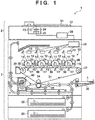
- FIG. 1 is an overview cross-sectional view of an image forming apparatus 1.
- the image forming apparatus 1 has an image reader 2 and a printer 3.
- the image reader 2 is a reader device for reading an original or a test chart.
- a light source 23 irradiates light on an original 21 placed on a platen glass 22.
- An optical system 24 guides a reflected light from the original 21 to a CCD sensor 25 causing an image to be formed.
- CCD is an abbreviation for charge-coupled device.
- the CCD sensor 25 generates color component signals for red, green, and blue.
- An image processing unit 28 executes image processing (example: shading correction or the like) on an image signal obtained by the CCD sensor 25, and outputs it to a printer controller 29 of the printer 3.
- the printer 3 forms toner images on a sheet S based on the image data.
- the printer 3 has an image forming unit 10 for forming toner images of each color out of Y (yellow), M (magenta), C (cyan), and Bk (black).
- the image forming unit 10 is provided with an image forming station for forming a yellow image, an image forming station for forming a magenta image, an image forming station for forming a cyan image, and an image forming station for forming a black image.
- the printer 3 of the present invention is not limited to a color printer for forming a full-color image, and may be a monochrome printer for forming a monochrome image, for example. As illustrated by FIG.
- the image forming station is provided with a photosensitive drum 11.
- the photosensitive drum 11 functions as a photosensitive member.
- a charger unit 12, an exposure unit 13, a developing unit 14, a primary transfer unit 17, and a drum cleaner 15 are arranged around the photosensitive drum 11.
- the charger unit 12 is provided with a charging roller for charging the surface potential of the photosensitive drum 11 to a predetermined charging potential.
- the exposure unit 13 is provided with a light source, a mirror, and a lens.
- the developing unit 14 is provided with a housing for housing a developing agent (toner), and a developing roller for carrying the developing agent in the housing. A developing voltage is applied to the developing roller.
- the primary transfer unit 17 is provided with a transfer blade to which a transfer bias (primary) is supplied. Note that configuration may be such that the primary transfer unit 17 is provided with a transfer roller instead of a transfer blade.
- the drum cleaner 15 is provided with a cleaning blade for removing toner from the surface of the photosensitive drum 11.
- the black image forming station forms a toner image. Note that because processes in which image forming stations for colors other than black form toner images are similar processes, description thereof is omitted here.
- the charger unit 12 causes the surface of the photosensitive drum 11 to be charged uniformly.
- the exposure unit 13 exposes the surface of the photosensitive drum 11 based on image data outputted from the printer controller 29. Thereby, an electrostatic latent image is formed on the photosensitive drum 11.
- the developing unit 14 forms a toner image by developing by causing toner to adhere to the electrostatic latent image.
- the primary transfer unit 17 transfers the toner image carried on the photosensitive drum 11 to an intermediate transfer belt 31.
- the intermediate transfer belt 31 functions as an intermediate transfer member to which the toner image is transferred.
- the intermediate transfer belt 31 is turned by three rollers 34, 36, and 37.
- the drum cleaner 15 removes toner remaining on the photosensitive drum 11 that was not transferred to the intermediate transfer belt 31 by the primary transfer unit 17.
- Sheets S are stacked on a feeding cassette 20 or a multi-feed tray 30.
- Feeding rollers feed a sheet S from the feeding cassette 20 or the multi-feed tray 30.
- a sheet S fed by the feeding roller is conveyed toward registration rollers 26 by conveyance rollers.
- the registration rollers 26 convey the sheet S to a transferring nip portion (transfer portion) between the intermediate transfer belt 31 and a secondary transfer unit 27 so that the toner image on the intermediate transfer belt 31 is transferred to a target position of the sheet S.
- the secondary transfer unit 27 is provided with a secondary transfer roller to which a (secondary) transfer bias is supplied.
- the secondary transfer unit 27 transfers the toner image on the intermediate transfer belt 31 to the sheet S at the transferring nip portion.
- a transfer cleaner 35 is provided with a cleaning blade for removing toner from the surface of the intermediate transfer belt 31.
- the transfer cleaner 35 removes toner remaining on the intermediate transfer belt 31 that was not transferred to the sheet S at the transferring nip portion.
- a fixing device 40 is provided with a heating roller having a heater and a pressure roller for pressing the sheet S to the heating roller.
- a fixing nip portion for fixing the toner image to the sheet S is formed between the heating roller and the pressure roller. The sheet S to which the toner image has been transferred passes through the fixing nip portion.
- the fixing device 40 uses the heat of the heating roller and the pressure of the fixing nip portion to fix the toner image to the sheet S.
- the photosensitive drum 11, the charger unit 12, and the drum cleaner 15 provided in the printer 3 of the present embodiment are integrated as one process cartridge 50.
- the process cartridge 50 can be attached/released with respect to the printer 3.
- a user or a service person can easily replace the photosensitive drum 11, the charger unit 12, and the drum cleaner 15.
- the developing unit 14 can also be attached/released with respect to the printer 3.
- the primary transfer unit 17 and the intermediate transfer belt 31 are integrated as a transfer cartridge.
- the transfer cartridge can also be attached/released with respect to the printer 3.
- a user or a service person can easily replace the primary transfer unit 17 and the intermediate transfer belt 31.
- the transfer cleaner 35 may also be made capable of being attached/released with respect to the printer 3.
- Replacement parts of the present embodiment are the process cartridge 50, the developing unit 14 and a transfer cartridge.
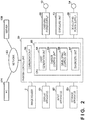
- FIG. 2 illustrates a control system of the image forming apparatus 1.
- the image forming apparatus 1 can be connected via a network to an external device such as a PC 124 or a server 128, via a network 123.
- PC is an abbreviation for personal computer.
- the printer controller 29 controls the image reader 2 and the printer 3.
- the printer controller 29 may be separated into an image processing unit for executing image processing, and a device controller for controlling the image reader 2 and the printer 3.
- a communication IF 55 is a communication circuit for receiving image data transferred from an external device (the PC 124 or the server 128) connected via a network, or transmitting various pieces of data from the image forming apparatus 1 to an external device (the PC 124 or the server 128).
- a CPU 60 is a control circuit for comprehensively controlling each unit of the image forming apparatus 1.
- the CPU 60 realizes each kind of function by executing control programs stored in a storage apparatus 63.
- some or all of the functions of the CPU 60 may be realized by hardware such as an ASIC, an FPGA or the like.
- ASIC is an abbreviation for application specific integrated circuit.
- FPGA is an abbreviation for field-programmable gate array.
- a display apparatus 61 is provided with a display for displaying various pieces of information such as a message, an image, or a moving image.
- An input apparatus 62 is provided with a numeric keypad, a start key, a stop key, and a read start button.
- the storage apparatus 63 is a memory such as a ROM or a RAM, and encompasses a bulk storage unit such as a hard disk drive.
- the CPU 60 performs image processing (data conversion processing, tone correction processing) on image data transferred from an external device or the image reader 2.
- the CPU 60 outputs the image data to which image processing has been performed to the exposure unit 13.
- a chart generation unit 64 controls the printer 3 to form a test image for identifying a replacement part on a sheet S.
- a sheet S to which a test image is formed is referred to as a test chart or simply as a chart.
- image data (pattern image data) for forming a test image is stored in the storage apparatus 63.
- a charging controller 65 controls a charging power supply 68 to apply a charging voltage to the charger unit 12.
- a developing controller 66 controls a developing power supply 69 to apply a developing voltage to the developing unit 14.
- a diagnostic unit 67 obtains a result of reading (read data) a chart read by the image reader 2, and determines a fault location based on the read data. Furthermore, the diagnostic unit 67 identifies a replacement part based on the determination result for the fault location.
- a vertical streak occurs in an output image.
- a vertical streak is a straight line image that extends parallel to a conveyance direction of the sheet S.
- the diagnostic unit 67 analyzes read data of a test image outputted from the image reader 2, and identifies a replacement part based on the density of the streak or the position of the streak that occurred in the test image. A test chart of the present embodiment is described below.
- the size of the test chart is assumed to be an A4 size (widthwise length 297 mm, conveyance-direction length 210 mm), for example. Note that the size of a test chart is not limited to the A4 size, and may be another size.
- the image forming apparatus 1 of the present embodiment outputs three test charts, for example, to determine a fault location (a causal part that causes a streak). However, the number of test charts may be one and may be a plurality of sheets, that is two or more.
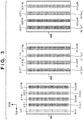
- FIG. 3 is a schematic view of three charts 301, 302, and 303 printed by the printer 3.
- the charts 301, 302, and 303 have a plain region W-P, digital patterns D-P, and analog patterns A1-P and A2-P.
- the digital patterns D-P and the analog patterns A1-P and A2-P are referred to as image patterns.
- the plain region W-P is referred to as a plain pattern.
- the color of toner used when forming each image pattern is a monochrome (a predetermined color), and is any one color of yellow, magenta, cyan, and black. As a result, it is possible to determine in which image forming station a fault location (a causal part that causes a streak) is present, from a result of reading an image pattern in which a streak image occurred.
- the length of each image pattern in the conveyance direction of the test charts is 30 mm, for example.
- the external diameter of a photosensitive drum 11 is 30 mm.
- An outer circumference of the photosensitive drum 11 is approximately 94.2 mm.
- the exposure unit 13 exposes the photosensitive drum 11.
- the digital patterns D-P are exposure images (toner images).
- the absolute value of the developing potential of the developing unit 14 is larger than the absolute value of the potential of an exposure region (a bright portion) in the photosensitive drum 11.
- the absolute value of the developing potential of the developing unit 14 is smaller than the absolute value of the potential of an exposure region (a dark portion) in the photosensitive drum 11.
- the relationship of potentials described above is the same as the relationship of potentials in a case where the printer 3 copies an original, for example.
- the exposure unit 13 does not expose the photosensitive drum 11.
- the analog patterns A1-P are non-exposure images (toner images).
- the absolute value of the developing potential of the developing unit 14 is larger than the absolute value of the surface potential of the photosensitive drum 11.
- a developing potential of the developing unit 14 is controlled to a negative value.
- the developing potential is lower than the surface potential of the photosensitive drum 11. For example, if the surface potential of the photosensitive drum 11 is greater than or equal to -100V and less than 0V, the developing potential is -300V.
- Camouflage patterns are formed on image patterns and the plain pattern.
- a camouflage pattern is a pattern for obscuring an image defect that occurs on the test chart.
- a camouflage pattern is formed on both of the image patterns and the plain pattern, but the present invention is not limited to this configuration.
- a configuration in which a camouflage pattern is formed on image patterns and a camouflage pattern is not formed on plain patterns may be employed.
- the present invention is not limited to a configuration where a camouflage pattern is formed on all image patterns.
- a configuration in which a camouflage pattern is not formed on an image pattern for yellow which it difficult to identify with visual observation, and a camouflage pattern is formed on image patterns of other colors (magenta, cyan, and black) may be employed.
- An image pattern on which a camouflage pattern is formed corresponds to a pattern image for detecting a fault location (a causal part where a streak occurs).
- a camouflage pattern W-Ca is formed on the plain region W-P.
- Camouflage patterns A1-Ca are formed on the analog patterns A1-P.
- Camouflage patterns A2-Ca are formed on the analog patterns A2-P.
- letters of Y, M, C, Bk added to the end of reference symbols indicating camouflage patterns indicate the color of the image pattern.
- An analog pattern A1-P-Y is formed by yellow toner.
- a camouflage pattern A1-Ca-Y indicates a camouflage pattern formed on an analog pattern A1-P-Y which is formed by yellow toner.
- the camouflage pattern A1-Ca-Y is a blue (mixed color) camouflage pattern, for example.
- the camouflage pattern may be a pattern so that another image defect different from an image defect for identifying a replacement part is obscured.
- camouflage A definition of camouflage is described here.
- Conventionally a technique where text or an image hidden in a copy of an original appears in order to prevent forgery of the original is known. With this technique, text or an image that is difficult for a human eye to distinguish is formed on an original.
- the text or image that appears on a copy of the original corresponds to a camouflage pattern.
- differences between a camouflage pattern and an image portion or differences between a camouflage pattern and a background portion where toner has not adhered are emphasized over differences between an image portion other than a camouflage pattern and a background portion. Accordingly, because the camouflage pattern will be relatively noticeable, the image portion or an outline of the image portion will be relatively obscured.
- FIG. 4 exemplifies various camouflage patterns added to image patterns. These are merely examples of camouflage patterns, and may be other patterns in the case of a pattern that obscures an image defect of an image pattern (a test image). Typically, an image pattern is formed based on a predetermined image signal value for all regions of the image pattern so that the density of the image pattern becomes a predetermined density. This is to cause an image defect to be apparent.
- a camouflage pattern is a specific pattern that is arranged regularly. For an image signal value for forming the specific pattern, an image signal value different from the predetermined image signal value is set, for example. As a result, the density of the specific pattern is different from the density of the image pattern (the predetermined density).
- the camouflage pattern is not limited to a regular specific patterns, and may be a random pattern.
- a camouflage pattern may be any of dotted line 1, dotted line 2, dotted line 3, polka dots, diagonal line 1, diagonal line 2, or intersecting lines.
- a camouflage pattern may be a diagonal dotted line pattern that combines dotted line 1 and diagonal line 1, for example.
- parameters for defining a camouflage pattern there are line intervals, dot intervals, line thickness, line density, contrast between lines and image pattern, or the like.
- a difference in density between the image pattern and the camouflage pattern and the shape of the pattern can be freely set.
- an image frequency of a random pattern can also be freely set.
- a camouflage pattern is not limited to a geometric pattern.
- a camouflage pattern may be a pattern that causes a viewer to envision image such as marble or a blue sky, and is referred to as a texture pattern, for example.
- a texture pattern uses changes in a color difference, a brightness difference and a density difference between a high density region and a low density region to obscure an image defect of a chart.
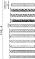
- FIG. 5 is an enlarged view of an image pattern on which a camouflage pattern is formed.
- a camouflage pattern Ca corresponding to dotted line 1 is formed with respect to an image pattern P.
- the width of the image pattern (P-Width) is 30 [mm].
- the camouflage pattern Ca is configured from a plurality of rectangular patterns.
- a distance (Space-X) between two rectangular patterns adjacent in the X direction (a sub scanning direction) is 1.8 [mm].
- a distance (Space-Y) between two rectangular patterns adjacent in the Y direction (a main scanning direction) is 0.7 [mm].
- the X direction (the sub scanning direction) is parallel to the conveyance direction of the sheet S, and is orthogonal to the Y direction (a main scanning direction).
- the width of the rectangular pattern (Ca-Width) is 0.25 [mm].
- the length of the rectangular pattern (Ca-Length) is 0.7 [mm].
- the width Ca-Width and the length Ca-Length may be 0.1 [mm] or more in order to make the camouflage pattern stand out visually.
- a camouflage effect increases.
- the camouflage effect increases, the area of a vertical streak detection region decreases.
- the width Ca-Width and the length Ca-Length of the rectangular pattern are decided so that it is possible to detect a vertical streak from read data of a test image on which rectangular patterns are formed. From experimentation, it is possible to detect a vertical streak from read data if the width Ca-Width and the length Ca-Length were less than or equal to 5.0 [mm].
- a vertical streak is an image defect for identifying a replacement part.
- two rectangular patterns adjacent in the X direction are shifted by a predetermined amount ⁇ Y in the Y direction.
- ⁇ Y is 0.3 [mm], for example.
- a longer side direction of the rectangular pattern is orthogonal with the X direction (the sub scanning direction). In other words, the longer side direction of the rectangular pattern and the longer side direction of a vertical streak differ. This is to suppress an increase of the camouflage effect, and a decrease of the area of a vertical streak detection region.
- the distance Space-X between rectangular patterns in the X direction and the distance Space-Y between rectangular patterns in the Y direction are decided to be distances having high sensitivity with respect to vision characteristics of a human.
- the distance Space-X and the distance Space-Y shorten, the area of a vertical streak detection region decreases. For this reason, the distances Space-X and Space-Y are decided so that it is possible to detect a vertical streak from read data of a chart on which rectangular patterns are formed.
- the color of the camouflage pattern Ca is set so that a color difference ⁇ E00 in visual observation is 3.0 or more with respect to a digital pattern D-P or analog patterns A1-P and A2-P. As the color difference ⁇ E00 increases, the camouflage effect also increases.
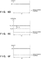
- FIG. 6A illustrates the potential of each position in the Y direction on the photosensitive drum 11 in a case where the printer 3 forms a digital pattern D-P.
- the potential of a position where the camouflage pattern D-Ca of the photosensitive drum 11 is formed is omitted.
- FIG. 6B illustrates a density dD of the digital pattern D-P formed on the sheet S, and a density d0 of a plain region W-P.
- the density d0 is the optical density of the sheet S.
- the charging controller 65 controls the charging power supply 68 so that the surface potential of the photosensitive drum 11, which is charged by the charger unit 12, becomes a potential Vd_D.
- the exposure unit 13 exposes the photosensitive drum 11 based on the pattern image data.
- the potential of the exposure region of the photosensitive drum 11 (a light portion potential) changes to V1_D.
- the potential of a non-exposure region of the photosensitive drum 11 is maintained at Vd_D.
- the developing controller 66 controls the developing power supply 69 so that the potential of the developing sleeve of the developing unit 14 becomes a developing potential Vdc_D which is a developing bias.
- the developing potential Vdc_D is set between a dark portion potential Vd_D and the light portion potential V1_D.
- a potential difference Vb corresponds to a potential difference between the developing potential Vdc D and the dark portion potential Vd_D.
- An image signal value of the pattern image data is decided in advance so that the optical density dD of the digital pattern D becomes 0.6, for example.
- the optical density dD of the digital pattern D-P may be any density if it is a density where a vertical streak is easy to detect.
- An image signal value of a digital pattern D-P is 50%, for example.
- FIG. 6C illustrates the potential of each position in the Y direction on the photosensitive drum 11 in a case where the printer 3 forms a first analog pattern A1-P.
- the potential of a position where the camouflage pattern Ca of the photosensitive drum 11 is formed is omitted.
- FIG. 6D illustrates a density dA1 of an analog pattern A1-P formed on the sheet S.
- the charging controller 65 controls the charging power supply 68 so that the surface potential of the photosensitive drum 11, which is charged by the charger unit 12, becomes a potential Vd_A1.
- the developing controller 66 controls the developing power supply 69 so that the potential of the developing sleeve of the developing unit 14 becomes a developing potential Vdc_A1.
- An absolute value of the developing potential Vdc_A1 is larger than an absolute value of a charging potential Vd_A1. Note that, when an analog pattern A1-P is formed, the exposure unit 13 does not irradiate a laser beam onto the photosensitive drum 11.
- a potential difference Vc_A1 (a development contrast Vc_A1) arises between the photosensitive drum 11 and the developing sleeve.
- the analog pattern A1-P is formed on the photosensitive drum 11. Note that margins are not formed on both sides of the analog pattern A1-P.
- the density of the analog pattern A1-P is decided based on the development contrast Vc_A1.
- An optical density dA1 of the analog pattern A1 is 0.6, for example.
- FIG. 6E illustrates the potential of each position in the Y direction on the photosensitive drum 11 in a case where the printer 3 forms a second analog pattern A2-P.
- the potential of a position where the camouflage pattern Ca of the photosensitive drum 11 is formed is omitted.
- FIG. 6F illustrates a density d1 of an analog pattern A2 formed on the sheet S.
- the charging controller 65 controls the charging power supply 68 so that the potential of the surface of the photosensitive drum 11 becomes a charging potential Vd_A2.
- the developing controller 66 controls the developing power supply 69 so that the potential of the developing sleeve of the developing unit 14 becomes a developing potential Vdc_A2.
- An absolute value of the developing potential Vdc_A2 is larger than an absolute value of the charging potential Vd_A2. Note that, when an analog pattern A2-P is formed, the exposure unit 13 does not irradiate a laser beam. As illustrated by FIG. 6F , a development contrast Vc_A2 arises between the photosensitive drum 11 and the developing sleeve.
- the analog pattern A2-P is formed on the photosensitive drum 11. Margins are not formed on both sides of the analog pattern A2-P.
- the density of the analog pattern A2-P is decided based on the development contrast Vc_A2.
- An optical density dA2 of the analog pattern A1 is 0.6, for example.
- the CPU 60 controls the developing controller 66 and the developing power supply 69 to adjust the development contrast Vc_A2.
- the second charging potential Vd_A2 for forming the analog pattern A2-P is set lower than the charging potential Vd_A1 for forming the analog pattern A1-P (
- a contribution rate of the charger unit 12 with respect to an image defect decreases for the analog pattern A2-P in comparison to the analog pattern A1-P.
- the diagnostic unit 67 compares streaks occurring with the analog pattern A1-P and the analog pattern A2-P to determine whether the cause of a streak is the charger unit 12 or the developing unit 14.
- the development contrast Vc_A1 of an analog pattern A1 and the development contrast Vc_A2 of an analog pattern A2 are the same. Accordingly, the optical density of the analog pattern A1-P and the optical density of the analog pattern A2-P are the same.
- the development contrast Vc_A1 of an analog pattern A1 and the development contrast Vc_A2 of an analog pattern A2 may differ.
- image forming conditions are controlled so that the optical density dD of the digital pattern D-P, the optical density dA1 of the analog pattern A1-P, and the optical density dA2 of the analog pattern A2-P become a predetermined density.
- the optical density dD of the digital pattern D-P, the optical density dA1 of the analog pattern A1-P, and the optical density dA2 of the analog pattern A2-P may each be different densities.
- the diagnostic unit 67 corrects the density of the streak occurring in each image pattern to determine a fault location (the causal part that generated the streak).
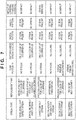
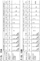
- FIG. 7 indicates vertical streak types, a replacement part or response method, a state of a plain portion, the color of the pattern where a streak occurs, the existence or absence of the occurrence of a streak for each of a digital pattern and an analog pattern, and an impact of reducing a charging potential for an analog pattern.
- a streak whose optical density is thinner than a predetermined density (0.6) is referred to as a white streak
- a streak whose optical density is thicker than the predetermined density (0.6) is referred to as a black streak.
- a developing coat defect streak indicated in FIG. 7 is a vertical streak that occurs because a developing coat is insufficient.
- FIG. 8A and FIG. 8B are views for describing a cause for a streak occurring due to a developing coat defect.
- the developing coat means that a developing agent is caused to adhere to the surface of a developing sleeve 142 at a uniform thickness.
- a magnet 141 functioning as a developing agent carrier is provided inside the developing sleeve 142.
- the developing sleeve 142 is supported by a developing container 143 to be able to rotate freely.
- a closest part 145 is a part at which the distance between the developing sleeve 142 and the photosensitive drum 11 is the closest.
- a regulation blade 146 is provided upstream of the closest part 145.
- the regulation blade 146 is arranged so that the distance in relation to the developing sleeve 142 is fixed, and regulates the amount of two-component developing agent supplied to the closest part 145.
- a foreign particle 148 such as dust or a hair may be clogged between the developing sleeve 142 and the regulation blade 146. In such a case, the foreign particle 148 impedes flow of the developing agent.
- FIG. 8C a vertical streak 151 where developing agent is not carried occurs on the developing sleeve 142.
- the developing agent is not supplied to the part facing the vertical streak 151 in the surface of the photosensitive drum 11 because there is no developing agent in the vertical streak 151. Therefore, a vertical streak 152 is such that a straight line which continues on the surface of the photosensitive drum 11 occurs.
- the unit to replace in order to resolve such a developing coat defect streak is the developing unit 14.
- a streak does not occur in a plain region W-P where an image pattern is not formed. Also, a color for which a streak occurs is only the color of the developing unit for which the developing coat defect occurred.
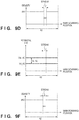
- FIG. 9A illustrates potentials at each main scanning position of the photosensitive drum 11 when a digital pattern D-P is formed.
- FIG. 9B illustrates optical density at each main scanning position of a sheet S when the digital pattern D is formed.
- FIG. 9C illustrates potentials at each main scanning position of the photosensitive drum 11 when an analog pattern A1-P is formed.
- FIG. 9D illustrates optical density at each main scanning position of a sheet S when an analog pattern A1-P is formed.
- FIG. 9E illustrates potentials at each main scanning position of the photosensitive drum 11 when an analog pattern A2-P is formed.
- FIG. 9F illustrates optical density at each main scanning position of a sheet S when an analog pattern A2-P is formed.
- a developing coat defect streak is due to developing agent not being supplied on the developing sleeve 142. Accordingly, a vertical streak occurs for all of the digital patterns D-P, and the analog patterns A1-P and A2-P. Furthermore, there is no difference between the density of a streak that occurs in the analog pattern A1-P, and the density of a streak that occurs in the analog pattern A2-P.
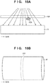
- FIG. 10A is a view for describing a mechanism where a white streak due to an exposure defect occurs.
- a dustproof glass 132 is provided in a light path along which a laser beam outputted from the exposure unit 13 passes.
- a foreign particle 135 such as a hair or toner adheres to a portion of the dustproof glass 132
- a laser beam irradiated onto the surface of the photosensitive drum 11 is blocked. That is, a vertical streak occurs when the potential of the electrostatic latent image of a part at which the laser beam is not irradiated due to the foreign particle 135 on the surface of the photosensitive drum 11 decreasing.
- This vertical streak becomes a white streak because it occurs due to the amount of adhered toner decreasing.
- the response method for reducing a white streak caused by an exposure defect is to perform cleaning work on the dustproof glass 132, or to replace the exposure unit 13.
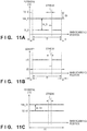
- FIG. 7 Characteristics of a white streak due to an exposure defect are described using FIG. 7 . Firstly, a streak does not occur in a plain region W-P where an image pattern is not formed. The color where a streak occurs in the digital pattern D-P is the color the exposure unit 13 that caused an exposure defect is responsible for.
- FIG. 11A illustrates potentials at each main scanning position of the photosensitive drum 11 when a digital pattern D-P is formed.
- FIG. 11B illustrates optical density at each main scanning position of a sheet S when the digital pattern D-P is formed.
- FIG. 11C illustrates potentials at each main scanning position of the photosensitive drum 11 when an analog pattern A1-P is formed.
- FIG. 11D illustrates optical density at each main scanning position of a sheet S when an analog pattern A1-P is formed.
- FIG. 11E illustrates potentials at each main scanning position of the photosensitive drum 11 when an analog pattern A2-P is formed.
- FIG. 11F illustrates optical density at each main scanning position of a sheet S when an analog pattern A2-P is formed.
- a white streak occurs due to an exposure defect (an amount of exposure light getting smaller). Accordingly, in the digital pattern D-P, a white streak occurs by a surface potential at a portion of main scanning positions of the photosensitive drum 11 getting higher than V1_D. In contrast, as illustrated by FIG. 11C through FIG. 11F , a streak does not occur for the analog patterns A1-P and A2-P because the analog patterns A1-P and A2-P are formed without applying exposure.
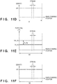
- FIG. 12A is a view that illustrates the surface potential (the charging potential) of the photosensitive drum 11.
- FIG. 12B is a view for illustrating a relationship between an image signal and optical density.
- the resistance of a charging member increases at main scanning positions for a portion of surface of the photosensitive drum 11, and the charging potential for these positions increases.
- a main scanning region at which the resistance became larger is called a high resistance portion.
- the resistance of the charging member gradually increases due to endurance, but the resistance of the charging member becomes partially lower even if a surface layer of the charging member is stripped off.
- FIG. 12A the resistance of a charging member at a portion of the main scanning region partially decreases, and the charging potential decreases. This portion is called a low resistance portion.
- the charging potential decreases as illustrated by FIG. 12B , even if each main scanning position of the photosensitive drum 11 is exposed using the same image signal, the density of the low resistance portion becomes higher than the predetermined density (0.6), and a black streak occurs.
- Characteristics of a charge defect streak are described using FIG. 7 . Firstly, a streak does not occur in a plain region W-P where an image pattern is not formed. The color out of YMCBk where a streak occurs is the color the charger unit 12 that caused a charge defect is responsible for.
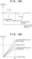
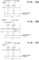
- FIG. 13A illustrates potentials at each main scanning position of the photosensitive drum 11 when a digital pattern D-P is formed.
- FIG. 13B illustrates optical density at each main scanning position of a sheet S when the digital pattern D is formed.
- FIG. 13C illustrates potentials at each main scanning position of the photosensitive drum 11 when an analog pattern A1-P is formed.
- FIG. 13D illustrates optical density at each main scanning position of a sheet S when an analog pattern A1-P is formed.
- FIG. 13E illustrates potentials at each main scanning position of the photosensitive drum 11 when an analog pattern A2-P is formed.
- FIG. 13F illustrates optical density at each main scanning position of a sheet S when an analog pattern A2-P is formed.
- the charging potential at the main scanning positions of a portion of the photosensitive drum 11, which is exposed by the digital pattern D-P differs from V1_D.
- a black streak occurs at a position where the charging potential is lower than V1_D
- a white streak occurs at a position where the charging potential is higher than V1_D.
- FIG. 13C and FIG. 13D a black streak or a white streak occur even with the analog pattern A1-P because the charging potential at a portion in the main scanning direction differs from Vd_A1. Because the charge defect occurs due to a charging member resistance difference, the charge defect is reduced by causing the charging potential of the charger unit 12 to decrease.
- the impact of a charge defect is smaller with the analog pattern A2-P, in comparison to the analog pattern A1-P. That is, the streak improves.
- a streak improving means that the difference between the optical density of the streak and the surrounding optical density (0.6) decreases. That is, when a streak improves, it becomes more difficult to notice the streak visually.
- FIG. 7 An inner surface of the intermediate transfer belt 31 that is used for a long period may be scraped, producing a powder.
- a portion of a part that configures the transfer cartridge may adhere to the surface of the rollers 36 and 37.
- FIG. 10B a portion of the intermediate transfer belt 31 is subject to a plasticity deformation to become a convex shape. Such a portion is called a convex portion 311.
- the convex portion 311 occurs on the intermediate transfer belt 31 in this way, it becomes difficult for both sides of the convex portion 311 to be in contact with the photosensitive drum 11 or a sheet S.
- a black streak occurs for the convex portion 311 because a lot of toner secondary transfers to the sheet S. Accordingly, the part to be replaced in order to resolve a streak due to a plasticity deformation of the intermediate transfer belt 31 is the transfer cartridge. Note that a white streak is not a streak of a white color, but rather is a pale streak where the density is low (there is less toner). Also, a black streak is a dense streak where the density is high (there is more toner).
- FIG. 7 Characteristics of a streak due to a plasticity deformation are described using FIG. 7 .
- a streak does not occur in a plain region W-P where an image pattern is not formed. Colors out of YMCBk where a streak occurs are all colors. This is because a streak of this type occurs in a secondary transfer unit.
- streaks occur even with the analog patterns A1-P and A2-P in addition to the digital pattern D-P.
- a streak caused by a defect in cleaning of the photosensitive drum 11 is a black streak.
- a portion of the cleaning blade of the drum cleaner 15 is defective. This defective part cannot scrape off toner remaining on the photosensitive drum 11 after the primary transfer. This becomes the cause of a black streak.
- This black streak occurs for a color that the drum cleaner 15, in which the cleaning defect occurred, is responsible for.
- a black streak caused by a cleaning defect occurs as an approximately straight line shaped streak in the plain region W-P. Accordingly, the part to be replaced in order to reduce streaks due to a cleaning defect of the photosensitive drum 11 is the process cartridge 50.
- FIG. 7 Characteristics of a streak due to a cleaning defect are described using FIG. 7 . Because streaks due to a cleaning defect occur, streaks also occur in the plain region W-P in which an image pattern is not formed.
- the color of a streak that occurs in the plain region W-P is the same color as the color of toner accumulated on the drum cleaner 15. Thus the type of the streak is a monochrome streak. Because the streak occurs even for a color for which an image is not formed, it occurs in patterns of all of the colors of yellow, magenta, cyan, and black. For example, when the drum cleaner 15 responsible for yellow is defective, a yellow streak occurs across all regions in the sub scanning direction of the sheet S, and thus a streak occurs in patterns of all colors. In addition, because there is no relationship between the existence or absence of exposure and a charging potential, streaks occur with any of the analog patterns A1-P and A2-P and the digital patterns D-P.
- a black streak that occurs due to a cleaning defect of the intermediate transfer belt 31 is described using FIG. 7 .
- a black streak occurs. This occurs because toner remaining on the intermediate transfer belt 31 after the secondary transfer cannot be scraped off.
- the color of a streak of this type is a color in which yellow, magenta, cyan, and black toner is mixed (a mixed color).
- the unit that should be replaced to reduce a black streak that occurs due to a defect in cleaning the intermediate transfer belt 31 is the transfer cleaner 35.
- FIG. 7 Characteristics of a streak that occurs due to a cleaning defect of the intermediate transfer belt 31 are described using FIG. 7 . Because a cleaning defect is the cause, streaks also occur in the plain region W-P in which an image pattern is not formed. A streak that occurs in the plain region W-P is in accordance with toner that has accumulated on the transfer cleaner 35, and thus the color of the streak is a mixture of colors of yellow, magenta, cyan, and black. In addition, because there is no relationship between the existence or absence of exposure and a charging potential, streaks occur with any of the analog patterns A1-P and A2-P and the digital patterns D-P.
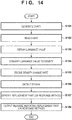
- FIG. 14 Processing for generating a chart and replacement part identification processing for identifying a replacement part are described using FIG. 14 .
- the CPU 60 Upon being input with an instruction for identifying a replacement part or an instruction for generating the charts 301, 302, and 303 from the input apparatus 62, the CPU 60 executes the following processing.
- step S101 the CPU 60 (the chart generation unit 64) controls the printer 3 to generate the charts 301 through 303.
- the CPU 60 controls the printer 3 to cause the digital patterns D-P, the analog patterns A1-P, the analog patterns A2-P, and the camouflage patterns W-Ca, D-Ca, A1-Ca, and A2-Ca to be formed on sheets S.
- the charging controller 65 controls the charging power supply 68 so that the surface potential of the photosensitive drum 11 becomes the charging potential Vd_D.
- the developing controller 66 controls the developing power supply 69 so that the potential of the developing sleeve of the developing unit 14 becomes a developing potential Vdc_D.
- the exposure unit 13 exposes the photosensitive drum 11 based on the camouflage pattern W-Ca. The exposure unit 13 does not exposure a position where the camouflage pattern is not to be formed in the plain region W-P. By this, the plain region W-P to which the camouflage pattern W-Ca has been added is formed on a sheet S (the chart 301).
- the charging controller 65 controls the charging power supply 68 so that the surface potential of the photosensitive drum 11y becomes the charging potential Vd_D.
- the exposure unit 13y exposes the photosensitive drum 11y based on pattern image data for forming the digital pattern D-P-Y.
- the developing controller 66 controls the developing power supply 69 so that the potential of the developing sleeve of the developing unit 14y becomes the developing potential Vdc D.
- the charging controller 65 controls the charging power supply 68 so that the surface potentials of the photosensitive drums 11m and 11c become the charging potential Vd_D.
- the exposure units 13m and 13c expose the photosensitive drums 11m and 11c based on pattern image data for forming the camouflage pattern D-Ca-Y.
- the developing controller 66 controls the developing power supply 69 so that the potential of the developing sleeves of the developing units 14m and 14c become the developing potential Vdc_D.
- the blue which is a complementary color for yellow, camouflage pattern D-Ca-Y (a mixed color pattern) is added to the digital pattern D-P-Y.
- the magenta digital pattern D-P-M, the cyan digital pattern D-P-C, and the black digital pattern D-P-Bk are similarly formed.
- a green camouflage pattern D-Ca-M (a mixed color pattern) is formed on the magenta digital pattern D-P-M
- a red camouflage pattern D-Ca-C (a mixed color pattern) is formed on the cyan digital pattern D-P-C.
- the green camouflage pattern D-Ca-Bk (a mixed color pattern) is formed on the black digital pattern D-P-Bk. This is because green is a color that has ⁇ E00 ⁇ 3.0 or more with respect to black.
- the charging controller 65 controls the charging power supply 68 so that the surface potential of the photosensitive drum 11y becomes the charging potential Vd_A1.
- the developing controller 66 controls the developing power supply 69 so that the potential of the developing sleeve of the yellow developing unit 14y becomes the developing potential Vdc_A1.
- the charging controller 65 controls the charging power supply 68 so that the surface potentials of the photosensitive drums 11m and 11c become the charging potential Vd Ca.
- the charging potential Vd Ca is set to a value that is the same as the charging potential Vd_D, for example.
- the exposure units 13m and 13c expose the photosensitive drums 11m and 11c, based on the pattern image data for forming the camouflage pattern A1-Ca-Y.
- the developing controller 66 controls the developing power supply 69 so that the potential of the developing sleeves of the developing units 14m and 14c becomes the developing potential Vdc_Ca.
- the developing potential Vdc Ca is set to a value that is the same as the developing potential Vdc_D, for example.
- camouflage pattern A1-Ca-Y When the camouflage pattern A1-Ca-Y is formed, the absolute value of the developing potential Vdc Ca is smaller than the absolute value of the charging potential Vd Ca. As a result, the blue, which is a complementary color for yellow, camouflage pattern A1-Ca-Y (a mixed color pattern) is added to the analog pattern A1-P-Y.
- the magenta analog pattern A1-P-M, the cyan analog pattern A1-P-C, and the black analog pattern A1-P-Bk are similarly formed.
- a green camouflage pattern A1-Ca-M (a mixed color pattern) is formed on the magenta analog pattern A1-P-M
- a red camouflage pattern A1-Ca-C (a mixed color pattern) is formed on the cyan analog pattern A1-P-C.
- the green camouflage pattern A1-Ca-Bk (a mixed color pattern) is formed on the black analog pattern A1-P-Bk. This is because green is a color that has ⁇ E00 ⁇ 3.0 or more with respect to black.
- the charging controller 65 controls the charging power supply 68 so that the surface potential of the photosensitive drum 11y becomes the charging potential Vd_A2.
- the developing controller 66 controls the developing power supply 69 so that the potential of the developing sleeve of the yellow developing unit 14y becomes the developing potential Vdc_A2.
- the charging controller 65 controls the charging power supply 68 so that the surface potentials of the photosensitive drums 11m and 11c become the charging potential Vd Ca.
- the exposure units 13m and 13c expose the photosensitive drums 11m and 11c, based on the pattern image data for forming the camouflage pattern A2-Ca-Y.
- the developing controller 66 controls the developing power supply 69 so that the potential of the developing sleeves of the developing units 14m and 14c becomes the developing potential Vdc_Ca.
- the absolute value of the developing potential Vdc Ca is smaller than the absolute value of the charging potential Vd Ca.
- the blue which is a complementary color for yellow, camouflage pattern A2-Ca-Y (a mixed color pattern) is added to the analog pattern A2-P-Y.
- the magenta analog pattern A2-P-M, the cyan analog pattern A2-P-C, and the black analog pattern A2-P-Bk are similarly formed.
- a green camouflage pattern A2-Ca-M (a mixed color pattern) is formed on the magenta analog pattern A2-P-M
- a red camouflage pattern A2-Ca-C (a mixed color pattern) is formed on the cyan analog pattern A2-P-C.
- the green camouflage pattern A2-Ca-Bk (a mixed color pattern) is formed on the black analog pattern A2-P-Bk. This is because green is a color that has ⁇ E00 ⁇ 3.0 or more with respect to black.
- step S102 the CPU 60 (the diagnostic unit 67) controls the image reader 2 to read the charts 301, 302, and 303.
- a user or a service person places the chart 301 on the platen glass 22, and presses the read start button of the input apparatus 62.
- the image reader 2 outputs the read data of the chart 301 to the diagnostic unit 67.
- the diagnostic unit 67 obtains the read data of the chart 301 outputted from the image reader 2.
- a user or a service person places the chart 302 and the chart 303 on the platen glass 22 and presses the read start button.
- the diagnostic unit 67 obtains the read data of the charts 302 and 303 outputted from the image reader 2.
- the read data for the charts 301, 302, and 303 is stored in the storage apparatus 63.
- step S103 the CPU 60 (the diagnostic unit 67) obtains luminance values from the read data.
- the position of the plain region W-P in the chart 301 and the positions of the digital patterns D-P-Y, D-P-M, D-P-C, and D-P-Bk are decided in advance.
- the diagnostic unit 67 extracts, from the read data of the chart 301 stored in the storage apparatus 63, read data for a detection range corresponding to the plain region W-P, and read data of detection ranges respectively corresponding to the digital patterns D-P-Y, D-P-M, D-P-C, and D-P-Bk.
- the positions of the analog patterns A1-P-Y, A1-P-M, A1-P-C, and A1-P-Bk in the chart 302 are decided in advance.
- the diagnostic unit 67 extracts, from the read data of the chart 302 stored in the storage apparatus 63, the read data of detection ranges respectively corresponding to the analog patterns A1-P-Y, A1-P-M, A1-P-C, and A1-P-Bk.
- the positions of the analog patterns A2-P-Y, A2-P-M, A2-P-C, and A2-P-Bk in the chart 303 are decided in advance.
- the diagnostic unit 67 extracts, from the read data of the chart 303 stored in the storage apparatus 63, the read data of detection ranges respectively corresponding to the analog patterns A2-P-Y, A2-P-M, A2-P-C, and A2-P-Bk.
- the diagnostic unit 67 extracts results of reading pixels in a complementary color relationship with the color of an image pattern.
- Read results for R pixels are extracted for a cyan image pattern.
- Read results for G pixels are extracted for a magenta image pattern.
- Read results for B pixels are extracted for a yellow image pattern.
- Read results for G pixels are extracted for black because it does not have a complementary color.
- These read results are luminance values.
- the image sensor of the image reader 2 is a CCD sensor, a CMOS sensor, or the like, and has R pixels, G pixels, and B pixels. Because a red filter is provided for an R pixel, it cannot read a camouflage pattern formed by red. By this, the diagnostic unit 67 can obtain read data in which the camouflage pattern has been removed or reduced from the image pattern read result. By a similar principle for magenta, yellow, and black, camouflage patterns are removed or reduced in image pattern read results.
- the diagnostic unit 67 obtains an average value of luminance values of each row of n pixels that configure a detection range. For example, assume that a detection range is configured by a pixel group having n rows ⁇ m columns. This pixel group has n pixels lined up in an X direction (the sub scanning direction), and m pixels lined up in a Y direction (the main scanning direction). Firstly, the diagnostic unit 67 obtains a sum of respective luminance values of the n pixels included in a first column, and divides this sum by n. As a result, an average luminance value of the first column in the detection range is obtained. The diagnostic unit 67 obtains an average luminance value for each of the second column to the m-th column, similarly to for the first column.
- step S104 the CPU 60 (the diagnostic unit 67) uses a density conversion table stored in the storage apparatus 63 to convert the m luminance values (averages) to densities.
- the density conversion table is stored in a ROM of the storage apparatus 63 at a time of shipment from a factory of the image forming apparatus 1.
- step S105 the CPU 60 (the diagnostic unit 67) decides a density change rate for each column.
- the density of the other column different from the target column is, for example, the density of a column adjacent to the target column.
- a column adjacent to an i-th column is an (i-1)-th column (i > 1).
- step S106 the CPU 60 (the diagnostic unit 67) detects a streak from a result of reading the charts 301 through 303. For example, the diagnostic unit 67 determines that there is a streak in a target column if the density change rate of the target column is greater than a threshold value.
- the threshold value is 7%, for example.
- a vertical streak may occur across a plurality of columns lined up in the Y direction (the main scanning direction).
- the diagnostic unit 67 does not detect a vertical streak in the i-1-th column, but detects a vertical streak in the subsequent i-th target column.
- the diagnostic unit 67 obtains the density change rate of the i+1-th target column after keeping the i-1-th column as the other column for the i+1-th target column in Equation (1). By this, it is possible to detect a vertical streak that occurs in the i+1-th column.
- step S105 and step S106 are repeatedly executed for each column from the first column until the m-th column.
- the diagnostic unit 67 distinguishes a streak whose density is greater than the predetermined density (0.6) as a black streak, and distinguishes a streak whose density is lower than the predetermined density (0.6) as a white streak.
- the diagnostic unit 67 stores, in the storage apparatus 63, the position at which the streak was detected in the Y direction (the main scanning direction), the color of the streak, and a luminance difference between a luminance corresponding to the predetermined density and the luminance of the streak as feature amounts of the streak. Note that the position where the streak was detected indicates where the streak occurred among the plain region W-P, the digital patterns D-P, and the analog patterns A1-P and A2-P.
- a charging potential for forming the analog patterns A1-P is higher than a charging potential for forming the analog patterns A2-P. Accordingly, if a luminance difference for a streak that occurs in the analog patterns A2-P is less than a luminance difference for a streak that occurs in the analog patterns A1-P, it is determined that the streak is due to a charge defect of the charger unit 12. In contrast, if a luminance difference for a streak that occurs in the analog patterns A2-P is greater than a luminance difference for a streak that occurs in the analog patterns A1-P, it is determined that the streak is due to a developing defect of the developing unit 14.
- the CPU 60 calculates an average value of the luminance values of each row for each of R pixels, G pixel, and B pixels.
- the average luminance value of the R pixels is converted to a density Dr.
- the average luminance value of the G pixels is converted to a density Dg.
- the average luminance value of the B pixels is converted to a density Db.
- the CPU 60 determines that a streak has occurred if at least one the densities Dr, Dg, and Db is greater than a predetermined density.
- the CPU 60 determines whether the color of the streak is a monochrome or a mixed color, based on a combination of the densities Dr, Dg, and Db.
- step S107 the CPU 60 (the diagnostic unit 67) identifies the cause of the streak and a replacement part (or a response method) based on a result of reading the charts 301 through 303 (a streak detection result).
- the diagnostic unit 67 determines a fault location (a causal part that generated a streak) based on the read data.
- the diagnostic unit 67 distinguishes the existence or absence of a streak and the color (monochrome (YMCBk) / mixed color, or the like) of the streak for each image pattern or plain region W-P based on streak feature amounts stored in the storage apparatus 63.
- the diagnostic unit 67 identifies the cause and the replacement part by comparing the result of distinguishing with an identification condition for identifying the cause and replacement part.
- step S108 the CPU 60 (the diagnostic unit 67) displays on the display apparatus 61 a message indicating the replacement part or the response method or transmits this message to the PC 124 or the server 128 via the communication IF 55. For example, a causal part that generated a streak is displayed on a display of the display apparatus 61.
- FIG. 15 illustrates an example of a message indicating a replacement part or a response method.
- the message includes information such as that a vertical streak (a streak that extends in the sub scanning direction) has occurred in the charts 301 through 303, a code indicated a cause, and a name of a replacement part.
- a user or a service person can easily understand what the cause of the streak is and what the replacement part is by referring to the message.
- the diagnostic unit 67 displays on the display apparatus 61 a message indicating that the image forming apparatus 1 is normal. In this way, a user, a service person or the like can easily comprehend what the replacement part is because they can know that a vertical streak occurred and what the replacement part is by the specific information.
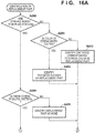
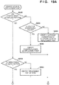
- FIGS. 16A and 16B are flowcharts illustrating details of processing for identifying a replacement part and a response method.
- the CPU 60 (the diagnostic unit 67) attempts to detect a vertical streak at each main scanning position (example: every 1 mm). Accordingly, a vertical streak may be detected at a plurality of main scanning positions. In addition, there is the possibility that the causes of a plurality of vertical streaks are respectively different. Accordingly, the CPU 60 (the diagnostic unit 67) identifies the cause and the replacement part for each streak. Note that the replacement part may be identified by identifying the cause of the occurrence of the streak.
- the determination processing illustrated in FIGS. 16A and 16B may be a set of identification conditions for identifying a replacement part or a cause.
- step S200 the CPU 60 reads feature amounts from the storage apparatus 63, and determines whether a streak is not present in the plain region W-P.
- the coordinates of the plain region W-P in the chart 301 are known beforehand.
- the CPU 60 compares the position of a streak and the coordinates of the plain region W-P to distinguish existence or absence of a streak in the plain region W-P. If there is a streak in the plain region W-P, the CPU 60 proceeds to step S201.
- step S201 the CPU 60 determines whether or not the color of the streak is a mixed color. If the color of the streak is a mixed color, the CPU 60 advances to step S202. In step S202, the CPU 60 distinguishes that the cause of the streak is a defect in cleaning the intermediate transfer belt 31, and identifies the transfer cleaner 35 as the replacement part. Meanwhile, if the color of the streak is a monochrome of any of YMCBk, the CPU 60 advances to step S203.
- step S203 the CPU 60 distinguishes the cause of the streak to be a cleaning defect of the photosensitive drum 11, and identifies the process cartridge 50 corresponding to the color of the streak as the replacement part. If a streak in the plain region W-P was not detected in step S200, the CPU 60 advances to step S204.
- step S204 the CPU 60 reads feature amounts from the storage apparatus 63, and determines whether a streak is present in the digital patterns D-P-Y through D-P-Bk.
- the coordinates of the digital patterns D-P-Y through D-P-Bk in the charts 301 through 303 are known beforehand.
- the CPU 60 compares the coordinates of the digital patterns D-P-Y through D-P-Bk with the position of a streak to distinguish existence or absence of a streak in the digital patterns D-P-Y through D-P-Bk. If there is no streak in any of the digital patterns D-P-Y through D-P-Bk, the CPU 60 advances to step S205.
- step S205 the CPU 60 identifies that there is no replacement part (normal). Meanwhile, upon detecting a streak in any of the digital patterns D-P-Y through D-P-Bk, the CPU 60 advances to step S206.
- step S206 the CPU 60 reads feature amounts from the storage apparatus 63, and determines whether or not a streak occurs in a particular color. This is the same as determining whether a streak occurs in all colors (all of the digital patterns D-P-Y through D-P-Bk). If a streak is occurring for all colors, the CPU 60 advances to step S207.
- step S207 the CPU 60 distinguishes that the cause of the streak is a plasticity deformation of the intermediate transfer belt 31, and identifies a transfer cartridge which includes the intermediate transfer belt 31 as the replacement part. Meanwhile, if a streak is occurring for a particular color, the CPU 60 advances to step S208.
- step S208 the CPU 60 determines whether a streak has occurred in an analog pattern A1-P of the same color as the color of a digital pattern D-P where a streak occurred. If there is no streak in the analog pattern A1-P, the CPU 60 advances to step S209.
- step S209 the CPU 60 distinguishes that the cause of the streak is an exposure defect, and identifies the exposure unit 13 corresponding to the color of the streak as the replacement part. Note that the CPU 60 may identify cleaning of the exposure unit 13 corresponding to the color of the streak as the response method.
- the CPU 60 advances to step S210.
- step S210 the CPU 60 determines whether a streak in an analog pattern A2-P has improved with respect to a streak in an analog pattern A1-P.
- the analog pattern A1 and the analog pattern A2 are of the same color.
- the CPU 60 may read feature amounts from the storage apparatus 63 and compare a luminance difference (a density difference) for a streak in the analog pattern A1-P with a luminance difference (a density difference) for a streak in the analog pattern A2. If the streak in the analog pattern A2-P has not improved in comparison to the streak in the analog pattern A1-P, the CPU 60 advances to step S211.
- step S211 the CPU 60 distinguishes that the cause of the streak is a developing coat defect, and identifies the developing unit 14 corresponding to the color of the streak as the replacement part. Meanwhile, if the density difference of the streak in the analog pattern A2-P is less than the density difference of the streak in the analog pattern A1-P, the streak has improved and the CPU 60 advances to step S212. In step S212, the CPU 60 distinguishes the cause of a streak to be a charge defect, and identifies the process cartridge 50 corresponding to the color of the streak as the replacement part.
- the CPU 60 generates the charts 301 through 303 and analyzes streaks that occur in the charts 301 through 303 to identify a replacement part and a cause of the streaks. Also, the CPU 60 may output a message indicating the cause of the streak and the replacement part to the display apparatus 61 or the like.
- the work time (downtime) necessary for maintenance may be significantly shortened. Also, because a part involved in the streak is identified, it may be that the replacement of a part that is not involved in the streak may be avoided. Thereby, maintenance costs may also be reduced as well as maintenance time.
- the message indicating the cause of the streak and the replacement part may be transmitted to the server 128 of the service person via the network. Because the service person can know what the replacement part is in advance, he or she can reliably bring the replacement part to perform the maintenance. Processing illustrated in FIGS. 16A and 16B for identifying, for example, a replacement part or a cause of a streak may be executed with a user or a service person visually observing the charts 301 through 303.
- a color printer is employed as an example, but the present embodiment may be applied to a monochrome printer.
- the CPU 60 generates the charts 301 through 303 and analyzes streaks that occur in the charts 301 through 303 to identify a replacement part and a cause of the streaks. Also, the CPU 60 may output a message indicating the cause of the streak and the replacement part to the display apparatus 61 or the like.
- the work time (downtime) necessary for maintenance may be significantly shortened. Also, because a part involved in the streak is identified, it may be that the replacement of a part that is not involved in the streak may be avoided. Thereby, maintenance costs may also be reduced as well as maintenance time.
- the message indicating the cause of the streak and the replacement part may be transmitted to the server 128 of the service person via the network. Because the service person can know what the replacement part is in advance, he or she can reliably bring the replacement part to perform the maintenance. Processing for identifying, for example, a replacement part or a cause of a streak may be executed with a user or a service person visually observing the charts 301 through 303.
- a color printer is employed as an example, but the present embodiment may be applied to a monochrome printer.
- the charts 301 through 303 illustrated in FIG. 3 are merely an example.
- the order of the plain region W-P, the digital pattern D-P, and the analog patterns A1-P and A2-P in the charts 301 through 303 may be another order. It is sufficient if the plain region W-P, the digital pattern D, and the analog patterns A1-P and A2-P are included in a chart. In particular, to identify whether the cause of a streak is the charger unit 12 or the developing unit 14, it is sufficient if the analog patterns A1-P and A2-P are included in a chart.
- a pattern image formed on a sheet S in accordance with the first embodiment is an example of a test image.
- the analog pattern A1 is an example of a first non-exposure image which is a toner image formed with a first charging potential (example: Vd_A1) being applied and without exposure being applied.
- the analog pattern A2 is an example of a second non-exposure image which is a toner image formed with a second charging potential different from the first charging potential (example: Vd_A2) being applied and without exposure being applied. It becomes possible to easily distinguish which of the charger unit 12 and the developing unit 14 to replace by using the two analog patterns having different charging potentials in this way.
- the image forming apparatus 1 which forms a test image by which it is possible to identify which of a charging unit and a developing unit should be replaced is provided.
- a user or service person may use the charts 301 through 303 to identify a replacement part visually, and the image forming apparatus 1 may read the charts 301 through 303 to identify a replacement part.
- camouflage patterns which are for obscuring an image defect that a user or a service person is not interested in, are added to the test images. Consequently, an image defect that is not necessary to identify the replacement part is obscured.
- a test image is formed by using toner of a single color.
- the color of a non-black test image and the color of a camouflage pattern added to the test image are in a complementary color relationship. This is because the camouflage pattern stands out with respect to the test image, and leads to a large camouflage effect.
- a green camouflage pattern may be added to a black test image. This is because there is no complementary color for black.
- the CCD sensor 25 is an example of a reader device that has R pixels, G pixels, and B pixels, and reads a test image.
- the diagnostic unit 67 of the CPU 60 compares a result of reading a test image with identification conditions for identifying a replacement part to thereby identify the replacement part.
- the CCD sensor 25 uses a result of reading G pixels for a black test image, uses a result of reading B pixels for a yellow test image, uses a result of reading G pixels for a magenta test image, and uses a result of reading R pixels for a cyan test image. Consequently, an impact of the camouflage pattern on a result of reading a test image is reduced.
- the image forming apparatus 1 performs charge processing in accordance with the charger unit 12 to form an analog pattern A1-P, but forms an analog pattern A2-P without performing charge processing in accordance with the charger unit 12. Consequently, the analog pattern A2-P becomes an image pattern that is not affected by the impact of a charge defect. For this reason, it is possible to detect even a slight charge defect by comparing an analog pattern A1-P formed by applying charge processing, and an analog pattern A2-P formed without applying charge processing. That is, it becomes possible to distinguish whether the cause of the streak is a charge defect or a developing coat defect.
- the second embodiment is similar to the first embodiment except for a method for forming an analog pattern A2-P and processing for identifying a replacement part. Accordingly description of portions already described is omitted.
- the charging controller 65 sets an applied voltage Vin to be applied to a charging member of the charger unit 12 to a discharge start voltage Vth or less
- the charging potential Vd of the photosensitive drum 11 becomes approximately 0 [V].
- the surface potential of the photosensitive drum 11 is controlled to be approximately 0[V] by setting the applied voltage Vin to a voltage (example: 0[V]) less than or equal to the discharge start voltage Vth (example: 400[V]).
- Charge on the surface of the photosensitive drum 11 may be removed in order to further reduce an impact of the charger unit 12 on the analog pattern A2-P.
- a pre-exposure light source (not shown) may expose the photosensitive drum 11 in relation to the surface of the photosensitive drum 11 which is cleaned by the drum cleaner 15. As a result the surface potential of the photosensitive drum 11 decreases to 0V.
- configuration may be taken such that charge processing is not applied to the photosensitive drum 11, by controlling the charging power supply 68 so that the charging controller 65 does not supply current to a metal wire.
- FIG. 17 illustrates an arrangement of analog patterns A1-P and A2-P in the second embodiment.
- the charts 302 and 303 are substituted by the charts 302' and 303'.
- the analog patterns A1-P-Y and A1-P-M for which charging is applied, and the analog patterns A2-P-C and A2-P-Bk for which charging is not applied are formed.
- the analog patterns A2-P-Y and A2-P-M for which charging is applied and the analog patterns A1-P-C and A1-P-Bk for which charging is not applied are formed.
- Two constraint conditions are imposed for colors that can be used for forming a camouflage pattern in the second embodiment.
- the first is that the color of a camouflage pattern must be a different color to the color of an analog pattern.
- toner of color other than yellow must be used for the camouflage pattern A1-Ca-Y added to the yellow analog pattern A1-P-Y for which charging is applied in the chart 302'.
- a camouflage pattern must be formed using colors for one or more types of toner that are different from the color of toner used to form an analog pattern.
- the second is that, so that time for switching charging potentials is sufficiently guaranteed, a color of toner of an analog pattern A2-P formed without charging being applied for the same sheet (page) must not be used.
- cyan and black are used for the analog patterns A2-P-C and A2-P-Bk for which charging is not applied. Accordingly, cyan and black must not be used for the camouflage pattern A1-Ca-Y. Therefore, only magenta can be used for the camouflage pattern A1-Ca-Y.
- FIG. 18A is a table illustrating combinations of image pattern colors and camouflage pattern colors. Based on the above constraint conditions, only yellow can be used for the camouflage pattern A1-Ca-M that is added to the magenta analog pattern A1-P-M of the chart 302'. Only black can be used for the camouflage pattern A1-Ca-C that is added to the cyan analog pattern A1-P-C of the chart 303'. Only cyan can be used for the camouflage pattern A1-Ca-Bk that is added to the black analog pattern A1-P-Bk of the chart 303'.
- camouflage pattern A2-Ca-C that is added to the cyan analog pattern A2-P-C for which charging is not applied with the chart 302', toner of a color other than cyan must be used based on the first condition.
- the camouflage pattern A2-Ca-C which is added onto the analog pattern A2-P-C must not be cyan or black. Accordingly it must be a yellow monochrome or a magenta monochrome.
- a yellow monochrome or a magenta monochrome must be used.
- camouflage pattern A2-Ca-Y that is added to the yellow analog pattern A2-P-Y for which charging is not applied with the chart 303', a cyan monochrome or a black monochrome must be used.
- camouflage pattern A2-Ca-M that is added to the magenta analog pattern A2-P-M for which charging is not applied with the chart 303', a cyan monochrome or a black monochrome must be used.
- analog patterns A1-P-Y, A1-P-M, A1-P-C, and A2-P-Bk may be formed on the chart 302', and the analog patterns A2-P-Y, A2-P-M, A2-P-C, and A1-P-Bk may be formed on the chart 303'.
- the above two constraint conditions are imposed even in this case.
- FIG. 18B is a table illustrating combinations of image pattern colors and camouflage pattern colors. As illustrated by FIG. 18B , there are respective toner colors that can be formed on each camouflage pattern in the chart 302'. However, there is no toner color that can form the camouflage pattern A1-Ca-Bk in the chart 303'. In other words, it is not possible to add a camouflage pattern to the analog pattern A1-P-Bk. Accordingly, in a case of arranging the analog patterns A1-P for which charging is applied and the analog patterns A2-P for which charging is not applied on two charts, it should be advantageous to divide YMCBk into two groups of two colors.
- FIGS. 19A and 19B are flowcharts illustrating details of processing for identifying a replacement part and a response method.
- step S210 is substituted with step S300.
- step S300 the CPU 60 reads feature amounts from the storage apparatus 63, and determines whether a streak is not present in the analog patterns A2-P. If there is a streak in the analog patterns A2-P, the CPU 60 advances to step S211. If there is no streak in the analog patterns A2-P, the CPU 60 advances to step S212.
- the CPU 60 identifies a charge defect as the cause of the streak, and identifies the process cartridge 50 including the charger unit 12 as the replacement part.
- the replacement part is a replacement part corresponding to the color of the streak. For example, if there is a streak in a yellow analog pattern A1-P but there is no streak in a yellow analog pattern A2-P, the process cartridge 50 that is responsible for yellow is identified as a replacement part.
- the charts 302' and 303' which include the analog patterns A1-P formed by applying charging, and the analog patterns A2-P formed without charging being applied are generated.
- the charts 302' and 303' which include the analog patterns A1-P formed by applying charging, and the analog patterns A2-P formed without charging being applied are generated.
- the CPU 60 uses toner of a color different from the color of toner of a first non-exposure image (for example: an analog pattern A1-P) to add to the first non-exposure image a camouflage pattern for obscuring an image defect that is not of interest.
- the CPU 60 uses toner of a color different from the color of toner of a second non-exposure image (for example: an analog pattern A2-P) to add a camouflage pattern to the second non-exposure image.
- the CPU 60 may form on the chart 302', which is a first sheet, the first non-exposure image of a first color, the first non-exposure image of a second color, the second non-exposure image of a third color, and the second non-exposure image of the fourth color. Furthermore, by controlling the image forming unit 10, the CPU 60 may form on the chart 303', which is a second sheet, the first non-exposure image of a first color, the first non-exposure image of a second color, the second non-exposure image of a third color, and the second non-exposure image of the fourth color.
- the colors of the camouflage patterns A1-Ca and A2-Ca are restricted.
- the color of the camouflage pattern A1-Ca-Y added to the first non-exposure image of the first color is the second color.
- the color of the camouflage pattern A1-Ca-M added to the first non-exposure image of the second color is the first color.
- the color of the camouflage pattern A2-Ca-C added to the second non-exposure image of the third color is the first color or the second color.
- the color of the camouflage pattern A2-Ca-Bk added to the second non-exposure image of the fourth color is the first color or the second color.
- the color of the camouflage pattern A2-Ca-Y added to the second non-exposure image of the first color is the third color or the fourth color.
- the color of the camouflage pattern A2-Ca-M added to the second non-exposure image of the second color is the third color or the fourth color.
- the color of the camouflage pattern A1-Ca-C added to the first non-exposure image of the third color is the fourth color.
- the color of the camouflage pattern A1-Ca-Bk added to the first non-exposure image of the fourth color is the third color.
- the image forming unit 10 has a first image forming unit for forming a toner image using toner of the first color, and a second image forming unit for forming a toner image using toner of the second color.
- the image forming unit 10 has a third image forming unit for forming a toner image using toner of the third color, and a fourth image forming unit for forming a toner image using toner of the fourth color.
- the first color is yellow
- the second color is magenta
- the third color is cyan
- the fourth color is black.
- Each image forming unit has a photosensitive drum 11, a charger unit 12, a developing unit 14, and a first cleaning unit (for example: the drum cleaner 15).
- An exposure unit (for example: the exposure unit 13) may be provided in each image forming unit, or a common exposure unit (for example: the exposure unit 13) may be provided for the four image forming units.
- Each developing unit 14 has a developing sleeve 142 for carrying a developing agent.
- the CPU 60 may form, on a first sheet, the first non-exposure image of the first color, the first non-exposure image of the second color, the first non-exposure image of the third color, and the first non-exposure image of the fourth color.
- the CPU 60 may form, on a second sheet, the second non-exposure image of the first color, the second non-exposure image of the second color, the second non-exposure image of the third color, and the second non-exposure image of the fourth color.
- the image forming apparatus 1 is not limited to a configuration in which the image reader 2 reads a chart. It may have a configuration where the printer 3 has a sensor for reading a chart on a conveyance path for conveying a sheet. The sensor is provided downstream of the fixing device 40 in the conveyance direction of the sheet. The CPU 60 conveys the chart along the conveyance path to the sensor, and reads the chart by the sensor. By this configuration, there is no burden where a user or a service person places a chart on the platen glass 22 of the image reader 2.
- Embodiment(s) of the present invention can also be realized by a computer of a system or apparatus that reads out and executes computer executable instructions (e.g., one or more programs) recorded on a storage medium (which may also be referred to more fully as a 'non-transitory computer-readable storage medium') to perform the functions of one or more of the above-described embodiment(s) and/or that includes one or more circuits (e.g., application specific integrated circuit (ASIC)) for performing the functions of one or more of the above-described embodiment(s), and by a method performed by the computer of the system or apparatus by, for example, reading out and executing the computer executable instructions from the storage medium to perform the functions of one or more of the above-described embodiment(s) and/or controlling the one or more circuits to perform the functions of one or more of the above-described embodiment(s).
- computer executable instructions e.g., one or more programs
- a storage medium which may also be referred to more fully as
- the computer may comprise one or more processors (e.g., central processing unit (CPU), micro processing unit (MPU)) and may include a network of separate computers or separate processors to read out and execute the computer executable instructions.
- the computer executable instructions may be provided to the computer, for example, from a network or the storage medium.
- the storage medium may include, for example, one or more of a hard disk, a random-access memory (RAM), a read only memory (ROM), a storage of distributed computing systems, an optical disk (such as a compact disc (CD), digital versatile disc (DVD), or Blu-ray Disc (BD)TM), a flash memory device, a memory card, and the like.
Description
- The present invention relates to an image forming apparatus.
- When an image forming apparatus such as a printer is subject to use that applies stress over a long time, there is a possibility of a "defective image", which is an image different from a normal one due to degradation or the like of parts, occurring. Because it is difficult to auto-detect by sensors a "defective image" that occurs due to degradation or the like, there are many cases where these are pointed out by a user, and attempts to resolve the cause are made. Furthermore, it is difficult to describe a "defective image" with words. For example, if detailed information such as the color, direction, and size of a streak is not known, it is not possible to identify the cause of the streak. Accordingly, it is necessary for a service person to whom a user pointed out the "defective image" to directly confirm an output image that includes the "defective image". The service person will estimate a faulty location in the image forming apparatus, and must first return to a service location bringing a unit that is to be replaced. When such an exchange is performed, a cost is incurred by the travel of the service person. Furthermore, the user cannot use the image forming apparatus until the cause is resolved. Accordingly, the user's productivity will greatly decrease.
- A technique for controlling an image forming apparatus to form a pattern image of a predetermined density on a sheet, causing a reader device to read the pattern image, and identifying a unit that needs replacement based on read data of the pattern image is known (Japanese Patent Laid-Open No.
2017-83544 2017-83544
Further prior art can be found in documentUS 2017/219979 A1 , disclosing an image forming apparatus and a control method for the image forming apparatus. The image forming apparatus is configured to appropriately determine that an abnormality has occurred in a component. The image forming apparatus includes a charging device configured to charge a photosensitive drum, an exposure device configured to form an electrostatic latent image on the photosensitive drum charged by the charging device, a developing device including a carrying member configured to carry a toner and being configured to develop the electrostatic latent image using the toner to form a toner image, and a transfer portion configured to transfer the toner image onto a sheet. The image forming apparatus is configured to form a measurement image on the sheet, and to determine a unit that needs to be replaced based on a result of measuring the measurement image formed on the sheet. The measurement image includes a first measurement image and a second measurement image.
Further prior art can be found in documentUS 2015/192884 A1 , disclosing a further image forming apparatus and a causal part determination method. - The present invention is realized by an image forming apparatus as specified in
claims 1 and 7. - Further features of the present invention will become apparent from the dependent claims and the following description of exemplary embodiments (with reference to the attached drawings).
-
-
FIG. 1 is a view for describing an image forming apparatus. -
FIG. 2 is a view for describing a control system. -
FIG. 3 is a view for describing a chart. -
FIG. 4 is a view for describing a camouflage pattern. -
FIG. 5 is a view for describing a camouflage pattern. -
FIGS. 6A to 6F are views for describing a relationship among latent image potential, charging potential, and developing potential. -
FIG. 7 is a view for describing a relationship between types of streaks and replacement parts. -
FIGS. 8A to 8C are views for describing a defect of a developing coat. -
FIGS. 9A to 9F are views for describing a relationship among streaks, latent image potential, charging potential, and developing potential. -
FIGS. 10A and 10B are views for describing an exposure defect and a plasticity deformation. -
FIGS. 11A to 11F are views for describing a relationship among streaks, latent image potential, charging potential, and developing potential. -
FIGS. 12A to 12B are views for describing a relationship between a streak and a cleaning defect of a photosensitive drum. -
FIGS. 13A to 13F are views for describing a relationship among streaks, latent image potential, charging potential, and developing potential. -
FIG. 14 is a flowchart for illustrating processing for generating a chart and processing for identifying a replacement part. -
FIG. 15 is a view for describing an example of a message indicating a replacement part. -
FIGS. 16A and16B are flowcharts illustrating processing for identifying a replacement part. -
FIG. 17 is a view for describing arrangement of analog patterns. -
FIGS. 18A and 18B are tables for describing toner colors that can be used for camouflage patterns. -
FIGS. 19A and19B are flowcharts illustrating processing for identifying a replacement part. -
FIG. 1 is an overview cross-sectional view of animage forming apparatus 1. Theimage forming apparatus 1 has animage reader 2 and aprinter 3. Theimage reader 2 is a reader device for reading an original or a test chart. A light source 23 irradiates light on an original 21 placed on aplaten glass 22. Anoptical system 24 guides a reflected light from the original 21 to aCCD sensor 25 causing an image to be formed. CCD is an abbreviation for charge-coupled device. TheCCD sensor 25 generates color component signals for red, green, and blue. Animage processing unit 28 executes image processing (example: shading correction or the like) on an image signal obtained by theCCD sensor 25, and outputs it to aprinter controller 29 of theprinter 3. - The
printer 3 forms toner images on a sheet S based on the image data. Theprinter 3 has animage forming unit 10 for forming toner images of each color out of Y (yellow), M (magenta), C (cyan), and Bk (black). Note that theimage forming unit 10 is provided with an image forming station for forming a yellow image, an image forming station for forming a magenta image, an image forming station for forming a cyan image, and an image forming station for forming a black image. In addition, theprinter 3 of the present invention is not limited to a color printer for forming a full-color image, and may be a monochrome printer for forming a monochrome image, for example. As illustrated byFIG. 1 , the four image forming stations corresponding to each color of Y, M, C, Bk are arranged in order from the left side of theimage forming unit 10. The configurations of the four image forming station are all the same, and thus the image forming station for forming a black image is described here. The image forming station is provided with aphotosensitive drum 11. Thephotosensitive drum 11 functions as a photosensitive member. Acharger unit 12, anexposure unit 13, a developingunit 14, aprimary transfer unit 17, and adrum cleaner 15 are arranged around thephotosensitive drum 11. Thecharger unit 12 is provided with a charging roller for charging the surface potential of thephotosensitive drum 11 to a predetermined charging potential. Theexposure unit 13 is provided with a light source, a mirror, and a lens. The developingunit 14 is provided with a housing for housing a developing agent (toner), and a developing roller for carrying the developing agent in the housing. A developing voltage is applied to the developing roller. Theprimary transfer unit 17 is provided with a transfer blade to which a transfer bias (primary) is supplied. Note that configuration may be such that theprimary transfer unit 17 is provided with a transfer roller instead of a transfer blade. Thedrum cleaner 15 is provided with a cleaning blade for removing toner from the surface of thephotosensitive drum 11. - Next, a process in which the black image forming station forms a toner image is described. Note that because processes in which image forming stations for colors other than black form toner images are similar processes, description thereof is omitted here. When image formation is started, the
photosensitive drum 11 rotates in the arrow symbol direction. Thecharger unit 12 causes the surface of thephotosensitive drum 11 to be charged uniformly. Theexposure unit 13 exposes the surface of thephotosensitive drum 11 based on image data outputted from theprinter controller 29. Thereby, an electrostatic latent image is formed on thephotosensitive drum 11. The developingunit 14 forms a toner image by developing by causing toner to adhere to the electrostatic latent image. Theprimary transfer unit 17 transfers the toner image carried on thephotosensitive drum 11 to anintermediate transfer belt 31. Theintermediate transfer belt 31 functions as an intermediate transfer member to which the toner image is transferred. Theintermediate transfer belt 31 is turned by threerollers drum cleaner 15 removes toner remaining on thephotosensitive drum 11 that was not transferred to theintermediate transfer belt 31 by theprimary transfer unit 17. - Sheets S are stacked on a feeding
cassette 20 or amulti-feed tray 30. Feeding rollers feed a sheet S from the feedingcassette 20 or themulti-feed tray 30. A sheet S fed by the feeding roller is conveyed towardregistration rollers 26 by conveyance rollers. Theregistration rollers 26 convey the sheet S to a transferring nip portion (transfer portion) between theintermediate transfer belt 31 and asecondary transfer unit 27 so that the toner image on theintermediate transfer belt 31 is transferred to a target position of the sheet S. Thesecondary transfer unit 27 is provided with a secondary transfer roller to which a (secondary) transfer bias is supplied. Thesecondary transfer unit 27 transfers the toner image on theintermediate transfer belt 31 to the sheet S at the transferring nip portion. Atransfer cleaner 35 is provided with a cleaning blade for removing toner from the surface of theintermediate transfer belt 31. Thetransfer cleaner 35 removes toner remaining on theintermediate transfer belt 31 that was not transferred to the sheet S at the transferring nip portion. A fixingdevice 40 is provided with a heating roller having a heater and a pressure roller for pressing the sheet S to the heating roller. A fixing nip portion for fixing the toner image to the sheet S is formed between the heating roller and the pressure roller. The sheet S to which the toner image has been transferred passes through the fixing nip portion. The fixingdevice 40 uses the heat of the heating roller and the pressure of the fixing nip portion to fix the toner image to the sheet S. - The
photosensitive drum 11, thecharger unit 12, and thedrum cleaner 15 provided in theprinter 3 of the present embodiment are integrated as oneprocess cartridge 50. Theprocess cartridge 50 can be attached/released with respect to theprinter 3. As a result, a user or a service person can easily replace thephotosensitive drum 11, thecharger unit 12, and thedrum cleaner 15. In addition, the developingunit 14 can also be attached/released with respect to theprinter 3. Furthermore, theprimary transfer unit 17 and theintermediate transfer belt 31 are integrated as a transfer cartridge. The transfer cartridge can also be attached/released with respect to theprinter 3. A user or a service person can easily replace theprimary transfer unit 17 and theintermediate transfer belt 31. Note that thetransfer cleaner 35 may also be made capable of being attached/released with respect to theprinter 3. Replacement parts of the present embodiment are theprocess cartridge 50, the developingunit 14 and a transfer cartridge. -
FIG. 2 illustrates a control system of theimage forming apparatus 1. Theimage forming apparatus 1 can be connected via a network to an external device such as aPC 124 or aserver 128, via anetwork 123. PC is an abbreviation for personal computer. Theprinter controller 29 controls theimage reader 2 and theprinter 3. Theprinter controller 29 may be separated into an image processing unit for executing image processing, and a device controller for controlling theimage reader 2 and theprinter 3. A communication IF 55 is a communication circuit for receiving image data transferred from an external device (thePC 124 or the server 128) connected via a network, or transmitting various pieces of data from theimage forming apparatus 1 to an external device (thePC 124 or the server 128). ACPU 60 is a control circuit for comprehensively controlling each unit of theimage forming apparatus 1. TheCPU 60 realizes each kind of function by executing control programs stored in astorage apparatus 63. Note that some or all of the functions of theCPU 60 may be realized by hardware such as an ASIC, an FPGA or the like. ASIC is an abbreviation for application specific integrated circuit. FPGA is an abbreviation for field-programmable gate array. Adisplay apparatus 61 is provided with a display for displaying various pieces of information such as a message, an image, or a moving image. Aninput apparatus 62 is provided with a numeric keypad, a start key, a stop key, and a read start button. Thestorage apparatus 63 is a memory such as a ROM or a RAM, and encompasses a bulk storage unit such as a hard disk drive. TheCPU 60 performs image processing (data conversion processing, tone correction processing) on image data transferred from an external device or theimage reader 2. TheCPU 60 outputs the image data to which image processing has been performed to theexposure unit 13. - The
CPU 60 realizes various functions, but a representative function related to the present embodiment is described here. Achart generation unit 64 controls theprinter 3 to form a test image for identifying a replacement part on a sheet S. In the following description, a sheet S to which a test image is formed is referred to as a test chart or simply as a chart. Note that image data (pattern image data) for forming a test image is stored in thestorage apparatus 63. A chargingcontroller 65 controls a chargingpower supply 68 to apply a charging voltage to thecharger unit 12. A developingcontroller 66 controls a developingpower supply 69 to apply a developing voltage to the developingunit 14. Adiagnostic unit 67 obtains a result of reading (read data) a chart read by theimage reader 2, and determines a fault location based on the read data. Furthermore, thediagnostic unit 67 identifies a replacement part based on the determination result for the fault location. - When a replacement time period is reached for a
process cartridge 50, a developingunit 14, or the like, a vertical streak occurs in an output image. A vertical streak is a straight line image that extends parallel to a conveyance direction of the sheet S. Thediagnostic unit 67 analyzes read data of a test image outputted from theimage reader 2, and identifies a replacement part based on the density of the streak or the position of the streak that occurred in the test image. A test chart of the present embodiment is described below. - The size of the test chart is assumed to be an A4 size (widthwise length 297 mm, conveyance-
direction length 210 mm), for example. Note that the size of a test chart is not limited to the A4 size, and may be another size. In addition, theimage forming apparatus 1 of the present embodiment outputs three test charts, for example, to determine a fault location (a causal part that causes a streak). However, the number of test charts may be one and may be a plurality of sheets, that is two or more. -
FIG. 3 is a schematic view of threecharts printer 3. Thecharts - The length of each image pattern in the conveyance direction of the test charts is 30 mm, for example. Note that the external diameter of a
photosensitive drum 11 is 30 mm. An outer circumference of thephotosensitive drum 11 is approximately 94.2 mm. - When the
printer 3 forms the digital patterns D-P, theexposure unit 13 exposes thephotosensitive drum 11. In other words, the digital patterns D-P are exposure images (toner images). The absolute value of the developing potential of the developingunit 14 is larger than the absolute value of the potential of an exposure region (a bright portion) in thephotosensitive drum 11. Note that the absolute value of the developing potential of the developingunit 14 is smaller than the absolute value of the potential of an exposure region (a dark portion) in thephotosensitive drum 11. The relationship of potentials described above is the same as the relationship of potentials in a case where theprinter 3 copies an original, for example. In contrast, when theprinter 3 forms the analog patterns A1-P and A2-P theexposure unit 13 does not expose thephotosensitive drum 11. In other words, the analog patterns A1-P are non-exposure images (toner images). In order to cause toner to adhere to thephotosensitive drum 11, the absolute value of the developing potential of the developingunit 14 is larger than the absolute value of the surface potential of thephotosensitive drum 11. For example, in a case where the image forming apparatus, which develops an electrostatic latent image using toner that is charged to a negative polarity, forms an analog pattern A1-P, a developing potential of the developingunit 14 is controlled to a negative value. In such a case, the developing potential is lower than the surface potential of thephotosensitive drum 11. For example, if the surface potential of thephotosensitive drum 11 is greater than or equal to -100V and less than 0V, the developing potential is -300V. - Camouflage patterns are formed on image patterns and the plain pattern. A camouflage pattern is a pattern for obscuring an image defect that occurs on the test chart. In the present embodiment a camouflage pattern is formed on both of the image patterns and the plain pattern, but the present invention is not limited to this configuration. For example, a configuration in which a camouflage pattern is formed on image patterns and a camouflage pattern is not formed on plain patterns may be employed. In addition, the present invention is not limited to a configuration where a camouflage pattern is formed on all image patterns. For example, a configuration in which a camouflage pattern is not formed on an image pattern for yellow which it difficult to identify with visual observation, and a camouflage pattern is formed on image patterns of other colors (magenta, cyan, and black) may be employed. An image pattern on which a camouflage pattern is formed corresponds to a pattern image for detecting a fault location (a causal part where a streak occurs).
- A camouflage pattern W-Ca is formed on the plain region W-P. Camouflage patterns A1-Ca are formed on the analog patterns A1-P. Camouflage patterns A2-Ca are formed on the analog patterns A2-P. Note that letters of Y, M, C, Bk added to the end of reference symbols indicating camouflage patterns indicate the color of the image pattern. An analog pattern A1-P-Y is formed by yellow toner. A camouflage pattern A1-Ca-Y indicates a camouflage pattern formed on an analog pattern A1-P-Y which is formed by yellow toner. Here, the camouflage pattern A1-Ca-Y is a blue (mixed color) camouflage pattern, for example. The camouflage pattern may be a pattern so that another image defect different from an image defect for identifying a replacement part is obscured.
- A definition of camouflage is described here. Conventionally, a technique where text or an image hidden in a copy of an original appears in order to prevent forgery of the original is known. With this technique, text or an image that is difficult for a human eye to distinguish is formed on an original. The text or image that appears on a copy of the original corresponds to a camouflage pattern. In a macro sense, differences between a camouflage pattern and an image portion or differences between a camouflage pattern and a background portion where toner has not adhered are emphasized over differences between an image portion other than a camouflage pattern and a background portion. Accordingly, because the camouflage pattern will be relatively noticeable, the image portion or an outline of the image portion will be relatively obscured.
-
FIG. 4 exemplifies various camouflage patterns added to image patterns. These are merely examples of camouflage patterns, and may be other patterns in the case of a pattern that obscures an image defect of an image pattern (a test image). Typically, an image pattern is formed based on a predetermined image signal value for all regions of the image pattern so that the density of the image pattern becomes a predetermined density. This is to cause an image defect to be apparent. A camouflage pattern is a specific pattern that is arranged regularly. For an image signal value for forming the specific pattern, an image signal value different from the predetermined image signal value is set, for example. As a result, the density of the specific pattern is different from the density of the image pattern (the predetermined density). In addition, the camouflage pattern is not limited to a regular specific patterns, and may be a random pattern. - A camouflage pattern may be any of dotted
line 1, dottedline 2, dottedline 3, polka dots,diagonal line 1,diagonal line 2, or intersecting lines. In addition, a camouflage pattern may be a diagonal dotted line pattern that combines dottedline 1 anddiagonal line 1, for example. As parameters for defining a camouflage pattern, there are line intervals, dot intervals, line thickness, line density, contrast between lines and image pattern, or the like. In addition, for a random pattern, a difference in density between the image pattern and the camouflage pattern and the shape of the pattern can be freely set. In addition, an image frequency of a random pattern can also be freely set. - A camouflage pattern is not limited to a geometric pattern. A camouflage pattern may be a pattern that causes a viewer to envision image such as marble or a blue sky, and is referred to as a texture pattern, for example. A texture pattern uses changes in a color difference, a brightness difference and a density difference between a high density region and a low density region to obscure an image defect of a chart.
-
FIG. 5 is an enlarged view of an image pattern on which a camouflage pattern is formed. In the image pattern illustrated inFIG. 5 , a camouflage pattern Ca corresponding to dottedline 1 is formed with respect to an image pattern P. The width of the image pattern (P-Width) is 30 [mm]. The camouflage pattern Ca is configured from a plurality of rectangular patterns. A distance (Space-X) between two rectangular patterns adjacent in the X direction (a sub scanning direction) is 1.8 [mm]. A distance (Space-Y) between two rectangular patterns adjacent in the Y direction (a main scanning direction) is 0.7 [mm]. Note that the X direction (the sub scanning direction) is parallel to the conveyance direction of the sheet S, and is orthogonal to the Y direction (a main scanning direction). The width of the rectangular pattern (Ca-Width) is 0.25 [mm]. The length of the rectangular pattern (Ca-Length) is 0.7 [mm]. The width Ca-Width and the length Ca-Length may be 0.1 [mm] or more in order to make the camouflage pattern stand out visually. As the width Ca-Width and the length Ca-Length increase, a camouflage effect increases. However, when the camouflage effect increases, the area of a vertical streak detection region decreases. For this reason, the width Ca-Width and the length Ca-Length of the rectangular pattern are decided so that it is possible to detect a vertical streak from read data of a test image on which rectangular patterns are formed. From experimentation, it is possible to detect a vertical streak from read data if the width Ca-Width and the length Ca-Length were less than or equal to 5.0 [mm]. - A vertical streak is an image defect for identifying a replacement part. As illustrated in
FIG. 5 , two rectangular patterns adjacent in the X direction are shifted by a predetermined amount ΔY in the Y direction. ΔY is 0.3 [mm], for example. A longer side direction of the rectangular pattern is orthogonal with the X direction (the sub scanning direction). In other words, the longer side direction of the rectangular pattern and the longer side direction of a vertical streak differ. This is to suppress an increase of the camouflage effect, and a decrease of the area of a vertical streak detection region. The distance Space-X between rectangular patterns in the X direction and the distance Space-Y between rectangular patterns in the Y direction are decided to be distances having high sensitivity with respect to vision characteristics of a human. However, as the distance Space-X and the distance Space-Y shorten, the area of a vertical streak detection region decreases. For this reason, the distances Space-X and Space-Y are decided so that it is possible to detect a vertical streak from read data of a chart on which rectangular patterns are formed. - The color of the camouflage pattern Ca is set so that a color difference ΔE00 in visual observation is 3.0 or more with respect to a digital pattern D-P or analog patterns A1-P and A2-P. As the color difference ΔE00 increases, the camouflage effect also increases.
-
FIG. 6A illustrates the potential of each position in the Y direction on thephotosensitive drum 11 in a case where theprinter 3 forms a digital pattern D-P. InFIG. 6A , the potential of a position where the camouflage pattern D-Ca of thephotosensitive drum 11 is formed is omitted.FIG. 6B illustrates a density dD of the digital pattern D-P formed on the sheet S, and a density d0 of a plain region W-P. The density d0 is the optical density of the sheet S. - The charging
controller 65 controls the chargingpower supply 68 so that the surface potential of thephotosensitive drum 11, which is charged by thecharger unit 12, becomes a potential Vd_D. Theexposure unit 13 exposes thephotosensitive drum 11 based on the pattern image data. As a result, the potential of the exposure region of the photosensitive drum 11 (a light portion potential) changes to V1_D. Note that the potential of a non-exposure region of the photosensitive drum 11 (a dark portion potential) is maintained at Vd_D. The developingcontroller 66 controls the developingpower supply 69 so that the potential of the developing sleeve of the developingunit 14 becomes a developing potential Vdc_D which is a developing bias. The developing potential Vdc_D is set between a dark portion potential Vd_D and the light portion potential V1_D. A potential difference Vb corresponds to a potential difference between the developing potential Vdc D and the dark portion potential Vd_D. As a result, toner does not adhere to a margin region. An image signal value of the pattern image data is decided in advance so that the optical density dD of the digital pattern D becomes 0.6, for example. The optical density dD of the digital pattern D-P may be any density if it is a density where a vertical streak is easy to detect. An image signal value of a digital pattern D-P is 50%, for example. -
FIG. 6C illustrates the potential of each position in the Y direction on thephotosensitive drum 11 in a case where theprinter 3 forms a first analog pattern A1-P. InFIG. 6C , the potential of a position where the camouflage pattern Ca of thephotosensitive drum 11 is formed is omitted.FIG. 6D illustrates a density dA1 of an analog pattern A1-P formed on the sheet S. - The charging
controller 65 controls the chargingpower supply 68 so that the surface potential of thephotosensitive drum 11, which is charged by thecharger unit 12, becomes a potential Vd_A1. The developingcontroller 66 controls the developingpower supply 69 so that the potential of the developing sleeve of the developingunit 14 becomes a developing potential Vdc_A1. An absolute value of the developing potential Vdc_A1 is larger than an absolute value of a charging potential Vd_A1. Note that, when an analog pattern A1-P is formed, theexposure unit 13 does not irradiate a laser beam onto thephotosensitive drum 11. As illustrated byFIG. 6C , a potential difference Vc_A1 (a development contrast Vc_A1) arises between thephotosensitive drum 11 and the developing sleeve. By this, the analog pattern A1-P is formed on thephotosensitive drum 11. Note that margins are not formed on both sides of the analog pattern A1-P. In addition, because thephotosensitive drum 11 is not exposed, the density of the analog pattern A1-P is decided based on the development contrast Vc_A1. An optical density dA1 of the analog pattern A1 is 0.6, for example. TheCPU 60 controls the developingcontroller 66 and the developingpower supply 69 to adjust the development contrast Vc_A1. As illustrated byFIG. 6D , an analog pattern A1 of the optical density dA1 (= 0.6) is formed on the sheet S. -
FIG. 6E illustrates the potential of each position in the Y direction on thephotosensitive drum 11 in a case where theprinter 3 forms a second analog pattern A2-P. InFIG. 6E , the potential of a position where the camouflage pattern Ca of thephotosensitive drum 11 is formed is omitted. -
FIG. 6F illustrates a density d1 of an analog pattern A2 formed on the sheet S. The chargingcontroller 65 controls the chargingpower supply 68 so that the potential of the surface of thephotosensitive drum 11 becomes a charging potential Vd_A2. The developingcontroller 66 controls the developingpower supply 69 so that the potential of the developing sleeve of the developingunit 14 becomes a developing potential Vdc_A2. An absolute value of the developing potential Vdc_A2 is larger than an absolute value of the charging potential Vd_A2. Note that, when an analog pattern A2-P is formed, theexposure unit 13 does not irradiate a laser beam. As illustrated byFIG. 6F , a development contrast Vc_A2 arises between thephotosensitive drum 11 and the developing sleeve. By this, the analog pattern A2-P is formed on thephotosensitive drum 11. Margins are not formed on both sides of the analog pattern A2-P. In addition, because exposure of thephotosensitive drum 11 is not applied, the density of the analog pattern A2-P is decided based on the development contrast Vc_A2. An optical density dA2 of the analog pattern A1 is 0.6, for example. TheCPU 60 controls the developingcontroller 66 and the developingpower supply 69 to adjust the development contrast Vc_A2. As illustrated byFIG. 6F , an analog pattern A2 of the optical density dA2 (= 0.6) is formed on the sheet S. - Here, the second charging potential Vd_A2 for forming the analog pattern A2-P is set lower than the charging potential Vd_A1 for forming the analog pattern A1-P (|Vd_A1|>|Vd_A2|). As a result, a contribution rate of the
charger unit 12 with respect to an image defect decreases for the analog pattern A2-P in comparison to the analog pattern A1-P. This is because thediagnostic unit 67 compares streaks occurring with the analog pattern A1-P and the analog pattern A2-P to determine whether the cause of a streak is thecharger unit 12 or the developingunit 14. In addition the development contrast Vc_A1 of an analog pattern A1 and the development contrast Vc_A2 of an analog pattern A2 are the same. Accordingly, the optical density of the analog pattern A1-P and the optical density of the analog pattern A2-P are the same. However, the development contrast Vc_A1 of an analog pattern A1 and the development contrast Vc_A2 of an analog pattern A2 may differ. - For the above description, image forming conditions are controlled so that the optical density dD of the digital pattern D-P, the optical density dA1 of the analog pattern A1-P, and the optical density dA2 of the analog pattern A2-P become a predetermined density. However, the optical density dD of the digital pattern D-P, the optical density dA1 of the analog pattern A1-P, and the optical density dA2 of the analog pattern A2-P may each be different densities. However, in this case the density of a streak that occurs for each image pattern differs. In a case of having this configuration, the
diagnostic unit 67 corrects the density of the streak occurring in each image pattern to determine a fault location (the causal part that generated the streak). - Using
FIG. 7 , vertical streaks that occur in a chart of the present embodiment are described.FIG. 7 indicates vertical streak types, a replacement part or response method, a state of a plain portion, the color of the pattern where a streak occurs, the existence or absence of the occurrence of a streak for each of a digital pattern and an analog pattern, and an impact of reducing a charging potential for an analog pattern. Note that a streak whose optical density is thinner than a predetermined density (0.6) is referred to as a white streak, and a streak whose optical density is thicker than the predetermined density (0.6) is referred to as a black streak. - A developing coat defect streak indicated in
FIG. 7 is a vertical streak that occurs because a developing coat is insufficient.FIG. 8A and FIG. 8B are views for describing a cause for a streak occurring due to a developing coat defect. The developing coat means that a developing agent is caused to adhere to the surface of a developingsleeve 142 at a uniform thickness. Amagnet 141 functioning as a developing agent carrier is provided inside the developingsleeve 142. The developingsleeve 142 is supported by a developingcontainer 143 to be able to rotate freely. Aclosest part 145 is a part at which the distance between the developingsleeve 142 and thephotosensitive drum 11 is the closest. In the rotation direction of the developingsleeve 142, aregulation blade 146 is provided upstream of theclosest part 145. Theregulation blade 146 is arranged so that the distance in relation to the developingsleeve 142 is fixed, and regulates the amount of two-component developing agent supplied to theclosest part 145. - As illustrated by
FIG. 8B , aforeign particle 148 such as dust or a hair may be clogged between the developingsleeve 142 and theregulation blade 146. In such a case, theforeign particle 148 impedes flow of the developing agent. As illustrated byFIG. 8C , avertical streak 151 where developing agent is not carried occurs on the developingsleeve 142. The developing agent is not supplied to the part facing thevertical streak 151 in the surface of thephotosensitive drum 11 because there is no developing agent in thevertical streak 151. Therefore, avertical streak 152 is such that a straight line which continues on the surface of thephotosensitive drum 11 occurs. As indicated byFIG. 7 , the unit to replace in order to resolve such a developing coat defect streak is the developingunit 14. - Furthermore, characteristics of a white streak that occurs due to a developing coat defect are described using
FIG. 7 . Firstly, a streak does not occur in a plain region W-P where an image pattern is not formed. Also, a color for which a streak occurs is only the color of the developing unit for which the developing coat defect occurred. -
FIG. 9A illustrates potentials at each main scanning position of thephotosensitive drum 11 when a digital pattern D-P is formed.FIG. 9B illustrates optical density at each main scanning position of a sheet S when the digital pattern D is formed.FIG. 9C illustrates potentials at each main scanning position of thephotosensitive drum 11 when an analog pattern A1-P is formed.FIG. 9D illustrates optical density at each main scanning position of a sheet S when an analog pattern A1-P is formed.FIG. 9E illustrates potentials at each main scanning position of thephotosensitive drum 11 when an analog pattern A2-P is formed.FIG. 9F illustrates optical density at each main scanning position of a sheet S when an analog pattern A2-P is formed. As these illustrate, a developing coat defect streak is due to developing agent not being supplied on the developingsleeve 142. Accordingly, a vertical streak occurs for all of the digital patterns D-P, and the analog patterns A1-P and A2-P. Furthermore, there is no difference between the density of a streak that occurs in the analog pattern A1-P, and the density of a streak that occurs in the analog pattern A2-P. - Next, a white streak due to an exposure defect indicated by
FIG. 7 is described.FIG. 10A is a view for describing a mechanism where a white streak due to an exposure defect occurs. Adustproof glass 132 is provided in a light path along which a laser beam outputted from theexposure unit 13 passes. When aforeign particle 135 such as a hair or toner adheres to a portion of thedustproof glass 132, a laser beam irradiated onto the surface of thephotosensitive drum 11 is blocked. That is, a vertical streak occurs when the potential of the electrostatic latent image of a part at which the laser beam is not irradiated due to theforeign particle 135 on the surface of thephotosensitive drum 11 decreasing. This vertical streak becomes a white streak because it occurs due to the amount of adhered toner decreasing. The response method for reducing a white streak caused by an exposure defect is to perform cleaning work on thedustproof glass 132, or to replace theexposure unit 13. - Characteristics of a white streak due to an exposure defect are described using
FIG. 7 . Firstly, a streak does not occur in a plain region W-P where an image pattern is not formed. The color where a streak occurs in the digital pattern D-P is the color theexposure unit 13 that caused an exposure defect is responsible for. -
FIG. 11A illustrates potentials at each main scanning position of thephotosensitive drum 11 when a digital pattern D-P is formed.FIG. 11B illustrates optical density at each main scanning position of a sheet S when the digital pattern D-P is formed.FIG. 11C illustrates potentials at each main scanning position of thephotosensitive drum 11 when an analog pattern A1-P is formed.FIG. 11D illustrates optical density at each main scanning position of a sheet S when an analog pattern A1-P is formed.FIG. 11E illustrates potentials at each main scanning position of thephotosensitive drum 11 when an analog pattern A2-P is formed.FIG. 11F illustrates optical density at each main scanning position of a sheet S when an analog pattern A2-P is formed. - As illustrated by
FIG. 11A or FIG. 11B , a white streak occurs due to an exposure defect (an amount of exposure light getting smaller). Accordingly, in the digital pattern D-P, a white streak occurs by a surface potential at a portion of main scanning positions of thephotosensitive drum 11 getting higher than V1_D. In contrast, as illustrated byFIG. 11C through FIG. 11F , a streak does not occur for the analog patterns A1-P and A2-P because the analog patterns A1-P and A2-P are formed without applying exposure. - A contact charging scheme in which the
photosensitive drum 11 is caused to be in contact with a charging member to perform charging is employed for thecharger unit 12 of the present embodiment. In the contact charging scheme, an additive agent such as silicone may adhere to the charging member due to insufficient cleaning at a position in the main scanning direction on the surface of thephotosensitive drum 11.FIG. 12A is a view that illustrates the surface potential (the charging potential) of thephotosensitive drum 11.FIG. 12B is a view for illustrating a relationship between an image signal and optical density. As illustrated byFIG. 12A , the resistance of a charging member increases at main scanning positions for a portion of surface of thephotosensitive drum 11, and the charging potential for these positions increases. A main scanning region at which the resistance became larger is called a high resistance portion. When the charging potential increases, as illustrated byFIG. 12B , even if each main scanning position of thephotosensitive drum 11 is exposed using the same image signal, the density of the high resistance portion becomes less than the predetermined density (0.6), and a white streak occurs. - Meanwhile, toner adheres to the charging member when a cleaning defect occurs in the main scanning position in a portion of the surface of the
photosensitive drum 11. The resistance of a part at which toner adheres in the surface of the charging member becomes lower. The resistance of the charging member gradually increases due to endurance, but the resistance of the charging member becomes partially lower even if a surface layer of the charging member is stripped off. As a result, as illustrated byFIG. 12A , the resistance of a charging member at a portion of the main scanning region partially decreases, and the charging potential decreases. This portion is called a low resistance portion. When the charging potential decreases, as illustrated byFIG. 12B , even if each main scanning position of thephotosensitive drum 11 is exposed using the same image signal, the density of the low resistance portion becomes higher than the predetermined density (0.6), and a black streak occurs. - Characteristics of a charge defect streak are described using
FIG. 7 . Firstly, a streak does not occur in a plain region W-P where an image pattern is not formed. The color out of YMCBk where a streak occurs is the color thecharger unit 12 that caused a charge defect is responsible for. -
FIG. 13A illustrates potentials at each main scanning position of thephotosensitive drum 11 when a digital pattern D-P is formed.FIG. 13B illustrates optical density at each main scanning position of a sheet S when the digital pattern D is formed.FIG. 13C illustrates potentials at each main scanning position of thephotosensitive drum 11 when an analog pattern A1-P is formed.FIG. 13D illustrates optical density at each main scanning position of a sheet S when an analog pattern A1-P is formed.FIG. 13E illustrates potentials at each main scanning position of thephotosensitive drum 11 when an analog pattern A2-P is formed.FIG. 13F illustrates optical density at each main scanning position of a sheet S when an analog pattern A2-P is formed. - As illustrated by
FIG. 13A and FIG. 13B , the charging potential at the main scanning positions of a portion of thephotosensitive drum 11, which is exposed by the digital pattern D-P, differs from V1_D. A black streak occurs at a position where the charging potential is lower than V1_D, and a white streak occurs at a position where the charging potential is higher than V1_D. As illustrated byFIG. 13C andFIG. 13D , a black streak or a white streak occur even with the analog pattern A1-P because the charging potential at a portion in the main scanning direction differs from Vd_A1. Because the charge defect occurs due to a charging member resistance difference, the charge defect is reduced by causing the charging potential of thecharger unit 12 to decrease. As illustrated byFIG. 13E and FIG. 13F , the impact of a charge defect is smaller with the analog pattern A2-P, in comparison to the analog pattern A1-P. That is, the streak improves. A streak improving means that the difference between the optical density of the streak and the surrounding optical density (0.6) decreases. That is, when a streak improves, it becomes more difficult to notice the streak visually. - Next, a streak due to a plasticity deformation of the
intermediate transfer belt 31 indicated byFIG. 7 is described. An inner surface of theintermediate transfer belt 31 that is used for a long period may be scraped, producing a powder. For example, a portion of a part that configures the transfer cartridge may adhere to the surface of therollers FIG. 10B , a portion of theintermediate transfer belt 31 is subject to a plasticity deformation to become a convex shape. Such a portion is called aconvex portion 311. When theconvex portion 311 occurs on theintermediate transfer belt 31 in this way, it becomes difficult for both sides of theconvex portion 311 to be in contact with thephotosensitive drum 11 or a sheet S. Accordingly, it becomes difficult to secondary transfer a toner image to the sheet S at both side portions, and white streaks occur. A black streak occurs for theconvex portion 311 because a lot of toner secondary transfers to the sheet S. Accordingly, the part to be replaced in order to resolve a streak due to a plasticity deformation of theintermediate transfer belt 31 is the transfer cartridge. Note that a white streak is not a streak of a white color, but rather is a pale streak where the density is low (there is less toner). Also, a black streak is a dense streak where the density is high (there is more toner). - Characteristics of a streak due to a plasticity deformation are described using
FIG. 7 . Firstly, a streak does not occur in a plain region W-P where an image pattern is not formed. Colors out of YMCBk where a streak occurs are all colors. This is because a streak of this type occurs in a secondary transfer unit. In addition, because there is no relationship between the existence or absence of exposure and a charging potential, streaks occur even with the analog patterns A1-P and A2-P in addition to the digital pattern D-P. - A streak caused by a defect in cleaning of the
photosensitive drum 11 is a black streak. A portion of the cleaning blade of thedrum cleaner 15 is defective. This defective part cannot scrape off toner remaining on thephotosensitive drum 11 after the primary transfer. This becomes the cause of a black streak. This black streak occurs for a color that thedrum cleaner 15, in which the cleaning defect occurred, is responsible for. Note that a black streak caused by a cleaning defect occurs as an approximately straight line shaped streak in the plain region W-P. Accordingly, the part to be replaced in order to reduce streaks due to a cleaning defect of thephotosensitive drum 11 is theprocess cartridge 50. - Characteristics of a streak due to a cleaning defect are described using
FIG. 7 . Because streaks due to a cleaning defect occur, streaks also occur in the plain region W-P in which an image pattern is not formed. The color of a streak that occurs in the plain region W-P is the same color as the color of toner accumulated on thedrum cleaner 15. Thus the type of the streak is a monochrome streak. Because the streak occurs even for a color for which an image is not formed, it occurs in patterns of all of the colors of yellow, magenta, cyan, and black. For example, when thedrum cleaner 15 responsible for yellow is defective, a yellow streak occurs across all regions in the sub scanning direction of the sheet S, and thus a streak occurs in patterns of all colors. In addition, because there is no relationship between the existence or absence of exposure and a charging potential, streaks occur with any of the analog patterns A1-P and A2-P and the digital patterns D-P. - A black streak that occurs due to a cleaning defect of the
intermediate transfer belt 31 is described usingFIG. 7 . When a portion of a member (a blade or the like) that makes contact with theintermediate transfer belt 31 in thetransfer cleaner 35 is defective, a black streak occurs. This occurs because toner remaining on theintermediate transfer belt 31 after the secondary transfer cannot be scraped off. The color of a streak of this type is a color in which yellow, magenta, cyan, and black toner is mixed (a mixed color). Thus, the unit that should be replaced to reduce a black streak that occurs due to a defect in cleaning theintermediate transfer belt 31 is thetransfer cleaner 35. - Characteristics of a streak that occurs due to a cleaning defect of the
intermediate transfer belt 31 are described usingFIG. 7 . Because a cleaning defect is the cause, streaks also occur in the plain region W-P in which an image pattern is not formed. A streak that occurs in the plain region W-P is in accordance with toner that has accumulated on thetransfer cleaner 35, and thus the color of the streak is a mixture of colors of yellow, magenta, cyan, and black. In addition, because there is no relationship between the existence or absence of exposure and a charging potential, streaks occur with any of the analog patterns A1-P and A2-P and the digital patterns D-P. - Processing for generating a chart and replacement part identification processing for identifying a replacement part are described using
FIG. 14 . Upon being input with an instruction for identifying a replacement part or an instruction for generating thecharts input apparatus 62, theCPU 60 executes the following processing. - In step S101, the CPU 60 (the chart generation unit 64) controls the
printer 3 to generate thecharts 301 through 303. TheCPU 60 controls theprinter 3 to cause the digital patterns D-P, the analog patterns A1-P, the analog patterns A2-P, and the camouflage patterns W-Ca, D-Ca, A1-Ca, and A2-Ca to be formed on sheets S. - In the case of forming a plain region W-P, the charging
controller 65 controls the chargingpower supply 68 so that the surface potential of thephotosensitive drum 11 becomes the charging potential Vd_D. In a case of forming the plain region W-P, the developingcontroller 66 controls the developingpower supply 69 so that the potential of the developing sleeve of the developingunit 14 becomes a developing potential Vdc_D. To form the camouflage pattern W-Ca on the plain region W-P, theexposure unit 13 exposes thephotosensitive drum 11 based on the camouflage pattern W-Ca. Theexposure unit 13 does not exposure a position where the camouflage pattern is not to be formed in the plain region W-P. By this, the plain region W-P to which the camouflage pattern W-Ca has been added is formed on a sheet S (the chart 301). - Next, in a case of forming the yellow digital pattern D-P-Y, the charging
controller 65 controls the chargingpower supply 68 so that the surface potential of the photosensitive drum 11y becomes the charging potential Vd_D. The exposure unit 13y exposes the photosensitive drum 11y based on pattern image data for forming the digital pattern D-P-Y. In a case of forming the digital pattern D-P-Y, the developingcontroller 66 controls the developingpower supply 69 so that the potential of the developing sleeve of the developing unit 14y becomes the developing potential Vdc D. In order to superimpose the blue camouflage pattern D-Ca-Y (a mixed color pattern) on the digital pattern D-P-Y, the chargingcontroller 65 controls the chargingpower supply 68 so that the surface potentials of the photosensitive drums 11m and 11c become the charging potential Vd_D. The exposure units 13m and 13c expose the photosensitive drums 11m and 11c based on pattern image data for forming the camouflage pattern D-Ca-Y. In order to form the camouflage pattern D-Ca-Y, the developingcontroller 66 controls the developingpower supply 69 so that the potential of the developing sleeves of the developing units 14m and 14c become the developing potential Vdc_D. As a result, the blue, which is a complementary color for yellow, camouflage pattern D-Ca-Y (a mixed color pattern) is added to the digital pattern D-P-Y. - The magenta digital pattern D-P-M, the cyan digital pattern D-P-C, and the black digital pattern D-P-Bk are similarly formed. Here, a green camouflage pattern D-Ca-M (a mixed color pattern) is formed on the magenta digital pattern D-P-M, and a red camouflage pattern D-Ca-C (a mixed color pattern) is formed on the cyan digital pattern D-P-C. However, because there is no complementary color for black, the green camouflage pattern D-Ca-Bk (a mixed color pattern) is formed on the black digital pattern D-P-Bk. This is because green is a color that has ΔE00 ≥ 3.0 or more with respect to black.
- In a case of forming a yellow analog pattern A1-P-Y, the charging
controller 65 controls the chargingpower supply 68 so that the surface potential of the photosensitive drum 11y becomes the charging potential Vd_A1. In a case of forming the yellow analog pattern A1-P-Y, the developingcontroller 66 controls the developingpower supply 69 so that the potential of the developing sleeve of the yellow developing unit 14y becomes the developing potential Vdc_A1. In order to superimpose the blue camouflage pattern A1-Ca-Y (a mixed color pattern) on the yellow analog pattern A1-P-Y, the chargingcontroller 65 controls the chargingpower supply 68 so that the surface potentials of the photosensitive drums 11m and 11c become the charging potential Vd Ca. The charging potential Vd Ca is set to a value that is the same as the charging potential Vd_D, for example. The exposure units 13m and 13c expose the photosensitive drums 11m and 11c, based on the pattern image data for forming the camouflage pattern A1-Ca-Y. In order to form the camouflage pattern Al-Ca-Y, the developingcontroller 66 controls the developingpower supply 69 so that the potential of the developing sleeves of the developing units 14m and 14c becomes the developing potential Vdc_Ca. The developing potential Vdc Ca is set to a value that is the same as the developing potential Vdc_D, for example. When the camouflage pattern A1-Ca-Y is formed, the absolute value of the developing potential Vdc Ca is smaller than the absolute value of the charging potential Vd Ca. As a result, the blue, which is a complementary color for yellow, camouflage pattern A1-Ca-Y (a mixed color pattern) is added to the analog pattern A1-P-Y. - The magenta analog pattern A1-P-M, the cyan analog pattern A1-P-C, and the black analog pattern A1-P-Bk are similarly formed. Here, a green camouflage pattern A1-Ca-M (a mixed color pattern) is formed on the magenta analog pattern A1-P-M, and a red camouflage pattern A1-Ca-C (a mixed color pattern) is formed on the cyan analog pattern A1-P-C. However, because there is no complementary color for black, the green camouflage pattern A1-Ca-Bk (a mixed color pattern) is formed on the black analog pattern A1-P-Bk. This is because green is a color that has ΔE00 ≥3.0 or more with respect to black.
- In a case of forming a yellow analog pattern A2-P-Y, the charging
controller 65 controls the chargingpower supply 68 so that the surface potential of the photosensitive drum 11y becomes the charging potential Vd_A2. In a case of forming the yellow analog pattern A2-P-Y, the developingcontroller 66 controls the developingpower supply 69 so that the potential of the developing sleeve of the yellow developing unit 14y becomes the developing potential Vdc_A2. In order to superimpose the blue camouflage pattern A2-Ca-Y (a mixed color pattern) on the yellow analog pattern A2-P-Y, the chargingcontroller 65 controls the chargingpower supply 68 so that the surface potentials of the photosensitive drums 11m and 11c become the charging potential Vd Ca. The exposure units 13m and 13c expose the photosensitive drums 11m and 11c, based on the pattern image data for forming the camouflage pattern A2-Ca-Y. In order to form the camouflage pattern A2-Ca-Y, the developingcontroller 66 controls the developingpower supply 69 so that the potential of the developing sleeves of the developing units 14m and 14c becomes the developing potential Vdc_Ca. When the camouflage pattern A2-Ca-Y is formed, the absolute value of the developing potential Vdc Ca is smaller than the absolute value of the charging potential Vd Ca. As a result, the blue, which is a complementary color for yellow, camouflage pattern A2-Ca-Y (a mixed color pattern) is added to the analog pattern A2-P-Y. - The magenta analog pattern A2-P-M, the cyan analog pattern A2-P-C, and the black analog pattern A2-P-Bk are similarly formed. Here, a green camouflage pattern A2-Ca-M (a mixed color pattern) is formed on the magenta analog pattern A2-P-M, and a red camouflage pattern A2-Ca-C (a mixed color pattern) is formed on the cyan analog pattern A2-P-C. However, because there is no complementary color for black, the green camouflage pattern A2-Ca-Bk (a mixed color pattern) is formed on the black analog pattern A2-P-Bk. This is because green is a color that has ΔE00 ≥ 3.0 or more with respect to black.
- In step S102, the CPU 60 (the diagnostic unit 67) controls the
image reader 2 to read thecharts chart 301 on theplaten glass 22, and presses the read start button of theinput apparatus 62. As a result, theimage reader 2 outputs the read data of thechart 301 to thediagnostic unit 67. Thediagnostic unit 67 obtains the read data of thechart 301 outputted from theimage reader 2. Similarly a user or a service person places thechart 302 and thechart 303 on theplaten glass 22 and presses the read start button. Thediagnostic unit 67 obtains the read data of thecharts image reader 2. The read data for thecharts storage apparatus 63. - In step S103, the CPU 60 (the diagnostic unit 67) obtains luminance values from the read data. The position of the plain region W-P in the
chart 301 and the positions of the digital patterns D-P-Y, D-P-M, D-P-C, and D-P-Bk are decided in advance. Thediagnostic unit 67 extracts, from the read data of thechart 301 stored in thestorage apparatus 63, read data for a detection range corresponding to the plain region W-P, and read data of detection ranges respectively corresponding to the digital patterns D-P-Y, D-P-M, D-P-C, and D-P-Bk. In addition, the positions of the analog patterns A1-P-Y, A1-P-M, A1-P-C, and A1-P-Bk in thechart 302 are decided in advance. Thediagnostic unit 67 extracts, from the read data of thechart 302 stored in thestorage apparatus 63, the read data of detection ranges respectively corresponding to the analog patterns A1-P-Y, A1-P-M, A1-P-C, and A1-P-Bk. Similarly, the positions of the analog patterns A2-P-Y, A2-P-M, A2-P-C, and A2-P-Bk in thechart 303 are decided in advance. Thediagnostic unit 67 extracts, from the read data of thechart 303 stored in thestorage apparatus 63, the read data of detection ranges respectively corresponding to the analog patterns A2-P-Y, A2-P-M, A2-P-C, and A2-P-Bk. - Next, the
diagnostic unit 67 extracts results of reading pixels in a complementary color relationship with the color of an image pattern. Read results for R pixels are extracted for a cyan image pattern. Read results for G pixels are extracted for a magenta image pattern. Read results for B pixels are extracted for a yellow image pattern. Read results for G pixels are extracted for black because it does not have a complementary color. These read results are luminance values. Note that the image sensor of theimage reader 2 is a CCD sensor, a CMOS sensor, or the like, and has R pixels, G pixels, and B pixels. Because a red filter is provided for an R pixel, it cannot read a camouflage pattern formed by red. By this, thediagnostic unit 67 can obtain read data in which the camouflage pattern has been removed or reduced from the image pattern read result. By a similar principle for magenta, yellow, and black, camouflage patterns are removed or reduced in image pattern read results. - The
diagnostic unit 67 obtains an average value of luminance values of each row of n pixels that configure a detection range. For example, assume that a detection range is configured by a pixel group having n rows × m columns. This pixel group has n pixels lined up in an X direction (the sub scanning direction), and m pixels lined up in a Y direction (the main scanning direction). Firstly, thediagnostic unit 67 obtains a sum of respective luminance values of the n pixels included in a first column, and divides this sum by n. As a result, an average luminance value of the first column in the detection range is obtained. Thediagnostic unit 67 obtains an average luminance value for each of the second column to the m-th column, similarly to for the first column. - In step S104, the CPU 60 (the diagnostic unit 67) uses a density conversion table stored in the
storage apparatus 63 to convert the m luminance values (averages) to densities. The density conversion table is stored in a ROM of thestorage apparatus 63 at a time of shipment from a factory of theimage forming apparatus 1. - In step S105, the CPU 60 (the diagnostic unit 67) decides a density change rate for each column. The density change rate is decided based on the following equation, for example.

- Here, the density of the other column different from the target column is, for example, the density of a column adjacent to the target column. For example, a column adjacent to an i-th column is an (i-1)-th column (i > 1).
- In step S106, the CPU 60 (the diagnostic unit 67) detects a streak from a result of reading the
charts 301 through 303. For example, thediagnostic unit 67 determines that there is a streak in a target column if the density change rate of the target column is greater than a threshold value. The threshold value is 7%, for example. - A vertical streak may occur across a plurality of columns lined up in the Y direction (the main scanning direction). In a case where there is a vertical streak in both an i-th target column and an i+1-th target column, it is not possible to determine a vertical streak when Equation (1) is applied unchanged. Accordingly, a design as below is necessary. Assume that the
diagnostic unit 67 does not detect a vertical streak in the i-1-th column, but detects a vertical streak in the subsequent i-th target column. In such a case, thediagnostic unit 67 obtains the density change rate of the i+1-th target column after keeping the i-1-th column as the other column for the i+1-th target column in Equation (1). By this, it is possible to detect a vertical streak that occurs in the i+1-th column. Note that step S105 and step S106 are repeatedly executed for each column from the first column until the m-th column. - The
diagnostic unit 67 distinguishes a streak whose density is greater than the predetermined density (0.6) as a black streak, and distinguishes a streak whose density is lower than the predetermined density (0.6) as a white streak. Thediagnostic unit 67 stores, in thestorage apparatus 63, the position at which the streak was detected in the Y direction (the main scanning direction), the color of the streak, and a luminance difference between a luminance corresponding to the predetermined density and the luminance of the streak as feature amounts of the streak. Note that the position where the streak was detected indicates where the streak occurred among the plain region W-P, the digital patterns D-P, and the analog patterns A1-P and A2-P. A charging potential for forming the analog patterns A1-P is higher than a charging potential for forming the analog patterns A2-P. Accordingly, if a luminance difference for a streak that occurs in the analog patterns A2-P is less than a luminance difference for a streak that occurs in the analog patterns A1-P, it is determined that the streak is due to a charge defect of thecharger unit 12. In contrast, if a luminance difference for a streak that occurs in the analog patterns A2-P is greater than a luminance difference for a streak that occurs in the analog patterns A1-P, it is determined that the streak is due to a developing defect of the developingunit 14. - Processing as below is executed for a detection region of the plain region W-P. The
CPU 60 calculates an average value of the luminance values of each row for each of R pixels, G pixel, and B pixels. The average luminance value of the R pixels is converted to a density Dr. The average luminance value of the G pixels is converted to a density Dg. The average luminance value of the B pixels is converted to a density Db. TheCPU 60 determines that a streak has occurred if at least one the densities Dr, Dg, and Db is greater than a predetermined density. Furthermore, theCPU 60 determines whether the color of the streak is a monochrome or a mixed color, based on a combination of the densities Dr, Dg, and Db. - In step S107, the CPU 60 (the diagnostic unit 67) identifies the cause of the streak and a replacement part (or a response method) based on a result of reading the
charts 301 through 303 (a streak detection result). In other words, thediagnostic unit 67 determines a fault location (a causal part that generated a streak) based on the read data. For example, thediagnostic unit 67 distinguishes the existence or absence of a streak and the color (monochrome (YMCBk) / mixed color, or the like) of the streak for each image pattern or plain region W-P based on streak feature amounts stored in thestorage apparatus 63. Thediagnostic unit 67 identifies the cause and the replacement part by comparing the result of distinguishing with an identification condition for identifying the cause and replacement part. - In step S108, the CPU 60 (the diagnostic unit 67) displays on the display apparatus 61 a message indicating the replacement part or the response method or transmits this message to the
PC 124 or theserver 128 via the communication IF 55. For example, a causal part that generated a streak is displayed on a display of thedisplay apparatus 61. -
FIG. 15 illustrates an example of a message indicating a replacement part or a response method. The message includes information such as that a vertical streak (a streak that extends in the sub scanning direction) has occurred in thecharts 301 through 303, a code indicated a cause, and a name of a replacement part. A user or a service person can easily understand what the cause of the streak is and what the replacement part is by referring to the message. Note that if a vertical streak is not detected, thediagnostic unit 67 displays on the display apparatus 61 a message indicating that theimage forming apparatus 1 is normal. In this way, a user, a service person or the like can easily comprehend what the replacement part is because they can know that a vertical streak occurred and what the replacement part is by the specific information. -
FIGS. 16A and16B are flowcharts illustrating details of processing for identifying a replacement part and a response method. The CPU 60 (the diagnostic unit 67) attempts to detect a vertical streak at each main scanning position (example: every 1 mm). Accordingly, a vertical streak may be detected at a plurality of main scanning positions. In addition, there is the possibility that the causes of a plurality of vertical streaks are respectively different. Accordingly, the CPU 60 (the diagnostic unit 67) identifies the cause and the replacement part for each streak. Note that the replacement part may be identified by identifying the cause of the occurrence of the streak. The determination processing illustrated inFIGS. 16A and16B may be a set of identification conditions for identifying a replacement part or a cause. - In step S200, the
CPU 60 reads feature amounts from thestorage apparatus 63, and determines whether a streak is not present in the plain region W-P. The coordinates of the plain region W-P in thechart 301 are known beforehand. TheCPU 60 compares the position of a streak and the coordinates of the plain region W-P to distinguish existence or absence of a streak in the plain region W-P. If there is a streak in the plain region W-P, theCPU 60 proceeds to step S201. - In step S201, the
CPU 60 determines whether or not the color of the streak is a mixed color. If the color of the streak is a mixed color, theCPU 60 advances to step S202. In step S202, theCPU 60 distinguishes that the cause of the streak is a defect in cleaning theintermediate transfer belt 31, and identifies thetransfer cleaner 35 as the replacement part. Meanwhile, if the color of the streak is a monochrome of any of YMCBk, theCPU 60 advances to step S203. - In step S203, the
CPU 60 distinguishes the cause of the streak to be a cleaning defect of thephotosensitive drum 11, and identifies theprocess cartridge 50 corresponding to the color of the streak as the replacement part. If a streak in the plain region W-P was not detected in step S200, theCPU 60 advances to step S204. - In step S204, the
CPU 60 reads feature amounts from thestorage apparatus 63, and determines whether a streak is present in the digital patterns D-P-Y through D-P-Bk. The coordinates of the digital patterns D-P-Y through D-P-Bk in thecharts 301 through 303 are known beforehand. TheCPU 60 compares the coordinates of the digital patterns D-P-Y through D-P-Bk with the position of a streak to distinguish existence or absence of a streak in the digital patterns D-P-Y through D-P-Bk. If there is no streak in any of the digital patterns D-P-Y through D-P-Bk, theCPU 60 advances to step S205. - In step S205, the
CPU 60 identifies that there is no replacement part (normal). Meanwhile, upon detecting a streak in any of the digital patterns D-P-Y through D-P-Bk, theCPU 60 advances to step S206. - In step S206, the
CPU 60 reads feature amounts from thestorage apparatus 63, and determines whether or not a streak occurs in a particular color. This is the same as determining whether a streak occurs in all colors (all of the digital patterns D-P-Y through D-P-Bk). If a streak is occurring for all colors, theCPU 60 advances to step S207. - In step S207, the
CPU 60 distinguishes that the cause of the streak is a plasticity deformation of theintermediate transfer belt 31, and identifies a transfer cartridge which includes theintermediate transfer belt 31 as the replacement part. Meanwhile, if a streak is occurring for a particular color, theCPU 60 advances to step S208. - In step S208, the
CPU 60 determines whether a streak has occurred in an analog pattern A1-P of the same color as the color of a digital pattern D-P where a streak occurred. If there is no streak in the analog pattern A1-P, theCPU 60 advances to step S209. - In step S209, the
CPU 60 distinguishes that the cause of the streak is an exposure defect, and identifies theexposure unit 13 corresponding to the color of the streak as the replacement part. Note that theCPU 60 may identify cleaning of theexposure unit 13 corresponding to the color of the streak as the response method. When a streak has occurred in an analog pattern A1-P of the same color as the color where a streak occurred in the digital pattern D-P, theCPU 60 advances to step S210. - In step S210, the
CPU 60 determines whether a streak in an analog pattern A2-P has improved with respect to a streak in an analog pattern A1-P. Note that the analog pattern A1 and the analog pattern A2 are of the same color. For example, theCPU 60 may read feature amounts from thestorage apparatus 63 and compare a luminance difference (a density difference) for a streak in the analog pattern A1-P with a luminance difference (a density difference) for a streak in the analog pattern A2. If the streak in the analog pattern A2-P has not improved in comparison to the streak in the analog pattern A1-P, theCPU 60 advances to step S211. - In step S211, the
CPU 60 distinguishes that the cause of the streak is a developing coat defect, and identifies the developingunit 14 corresponding to the color of the streak as the replacement part. Meanwhile, if the density difference of the streak in the analog pattern A2-P is less than the density difference of the streak in the analog pattern A1-P, the streak has improved and theCPU 60 advances to step S212. In step S212, theCPU 60 distinguishes the cause of a streak to be a charge defect, and identifies theprocess cartridge 50 corresponding to the color of the streak as the replacement part. - In this way, the
CPU 60 generates thecharts 301 through 303 and analyzes streaks that occur in thecharts 301 through 303 to identify a replacement part and a cause of the streaks. Also, theCPU 60 may output a message indicating the cause of the streak and the replacement part to thedisplay apparatus 61 or the like. By this, it becomes possible for a user or a service person to easily recognize the cause of the streak and the replacement part. Thereby, the work time (downtime) necessary for maintenance may be significantly shortened. Also, because a part involved in the streak is identified, it may be that the replacement of a part that is not involved in the streak may be avoided. Thereby, maintenance costs may also be reduced as well as maintenance time. The message indicating the cause of the streak and the replacement part may be transmitted to theserver 128 of the service person via the network. Because the service person can know what the replacement part is in advance, he or she can reliably bring the replacement part to perform the maintenance. Processing illustrated inFIGS. 16A and16B for identifying, for example, a replacement part or a cause of a streak may be executed with a user or a service person visually observing thecharts 301 through 303. Here, a color printer is employed as an example, but the present embodiment may be applied to a monochrome printer. - In this way, the
CPU 60 generates thecharts 301 through 303 and analyzes streaks that occur in thecharts 301 through 303 to identify a replacement part and a cause of the streaks. Also, theCPU 60 may output a message indicating the cause of the streak and the replacement part to thedisplay apparatus 61 or the like. By this, it becomes possible for a user or a service person to easily recognize the cause of the streak and the replacement part. Thereby, the work time (downtime) necessary for maintenance may be significantly shortened. Also, because a part involved in the streak is identified, it may be that the replacement of a part that is not involved in the streak may be avoided. Thereby, maintenance costs may also be reduced as well as maintenance time. The message indicating the cause of the streak and the replacement part may be transmitted to theserver 128 of the service person via the network. Because the service person can know what the replacement part is in advance, he or she can reliably bring the replacement part to perform the maintenance. Processing for identifying, for example, a replacement part or a cause of a streak may be executed with a user or a service person visually observing thecharts 301 through 303. Here, a color printer is employed as an example, but the present embodiment may be applied to a monochrome printer. - The
charts 301 through 303 illustrated inFIG. 3 are merely an example. The order of the plain region W-P, the digital pattern D-P, and the analog patterns A1-P and A2-P in thecharts 301 through 303 may be another order. It is sufficient if the plain region W-P, the digital pattern D, and the analog patterns A1-P and A2-P are included in a chart. In particular, to identify whether the cause of a streak is thecharger unit 12 or the developingunit 14, it is sufficient if the analog patterns A1-P and A2-P are included in a chart. - A pattern image formed on a sheet S in accordance with the first embodiment is an example of a test image. The analog pattern A1 is an example of a first non-exposure image which is a toner image formed with a first charging potential (example: Vd_A1) being applied and without exposure being applied. The analog pattern A2 is an example of a second non-exposure image which is a toner image formed with a second charging potential different from the first charging potential (example: Vd_A2) being applied and without exposure being applied. It becomes possible to easily distinguish which of the
charger unit 12 and the developingunit 14 to replace by using the two analog patterns having different charging potentials in this way. That is, by the present embodiment, theimage forming apparatus 1 which forms a test image by which it is possible to identify which of a charging unit and a developing unit should be replaced is provided. Note that a user or service person may use thecharts 301 through 303 to identify a replacement part visually, and theimage forming apparatus 1 may read thecharts 301 through 303 to identify a replacement part. In particular, camouflage patterns, which are for obscuring an image defect that a user or a service person is not interested in, are added to the test images. Consequently, an image defect that is not necessary to identify the replacement part is obscured. - Basically, a test image is formed by using toner of a single color. The color of a non-black test image and the color of a camouflage pattern added to the test image are in a complementary color relationship. This is because the camouflage pattern stands out with respect to the test image, and leads to a large camouflage effect. A green camouflage pattern may be added to a black test image. This is because there is no complementary color for black. Note that the
CCD sensor 25 is an example of a reader device that has R pixels, G pixels, and B pixels, and reads a test image. Thediagnostic unit 67 of theCPU 60 compares a result of reading a test image with identification conditions for identifying a replacement part to thereby identify the replacement part. TheCCD sensor 25 uses a result of reading G pixels for a black test image, uses a result of reading B pixels for a yellow test image, uses a result of reading G pixels for a magenta test image, and uses a result of reading R pixels for a cyan test image. Consequently, an impact of the camouflage pattern on a result of reading a test image is reduced. - In the first embodiment, by generating the
charts 301 through 303 that include a plurality of analog patterns A1-P and A2-P having the same optical density but different charging potentials, it is identified whether the cause of a streak is thecharger unit 12 or the developingunit 14. However, it is difficult to detect a slight charge defect simply by causing the charging potential to differ. This is because with a slight charge defect, a difference between a streak in an analog pattern A1-P and a streak in an analog pattern A2-P does not become sufficiently large. - Accordingly, in the second embodiment, the
image forming apparatus 1 performs charge processing in accordance with thecharger unit 12 to form an analog pattern A1-P, but forms an analog pattern A2-P without performing charge processing in accordance with thecharger unit 12. Consequently, the analog pattern A2-P becomes an image pattern that is not affected by the impact of a charge defect. For this reason, it is possible to detect even a slight charge defect by comparing an analog pattern A1-P formed by applying charge processing, and an analog pattern A2-P formed without applying charge processing. That is, it becomes possible to distinguish whether the cause of the streak is a charge defect or a developing coat defect. Note that the second embodiment is similar to the first embodiment except for a method for forming an analog pattern A2-P and processing for identifying a replacement part. Accordingly description of portions already described is omitted. - When forming an analog pattern A2-P without performing charge processing in accordance with the
charger unit 12, it is difficult to add a camouflage pattern A2-Ca onto the analog pattern A2-P. This is because time for switching voltages is necessary. Accordingly, in the second embodiment, a pattern arrangement where it is possible to form an analog pattern A2-P without performing charge processing in accordance with thecharger unit 12, and add a camouflage pattern A2-Ca is proposed. - In a contact charging scheme, when the charging
controller 65 sets an applied voltage Vin to be applied to a charging member of thecharger unit 12 to a discharge start voltage Vth or less, the charging potential Vd of thephotosensitive drum 11 becomes approximately 0 [V]. In this way, in the second embodiment, the surface potential of thephotosensitive drum 11 is controlled to be approximately 0[V] by setting the applied voltage Vin to a voltage (example: 0[V]) less than or equal to the discharge start voltage Vth (example: 400[V]). - Charge on the surface of the
photosensitive drum 11 may be removed in order to further reduce an impact of thecharger unit 12 on the analog pattern A2-P. For example, a pre-exposure light source (not shown) may expose thephotosensitive drum 11 in relation to the surface of thephotosensitive drum 11 which is cleaned by thedrum cleaner 15. As a result the surface potential of thephotosensitive drum 11 decreases to 0V. In a case where a non-contact charging scheme is used, configuration may be taken such that charge processing is not applied to thephotosensitive drum 11, by controlling the chargingpower supply 68 so that the chargingcontroller 65 does not supply current to a metal wire. -
FIG. 17 illustrates an arrangement of analog patterns A1-P and A2-P in the second embodiment. In the second embodiment, differences with the first embodiment are that thecharts - Two constraint conditions are imposed for colors that can be used for forming a camouflage pattern in the second embodiment. The first is that the color of a camouflage pattern must be a different color to the color of an analog pattern. For example, for the camouflage pattern A1-Ca-Y added to the yellow analog pattern A1-P-Y for which charging is applied in the chart 302', toner of color other than yellow must be used. In other words, a camouflage pattern must be formed using colors for one or more types of toner that are different from the color of toner used to form an analog pattern. The second is that, so that time for switching charging potentials is sufficiently guaranteed, a color of toner of an analog pattern A2-P formed without charging being applied for the same sheet (page) must not be used. For example, cyan and black are used for the analog patterns A2-P-C and A2-P-Bk for which charging is not applied. Accordingly, cyan and black must not be used for the camouflage pattern A1-Ca-Y. Therefore, only magenta can be used for the camouflage pattern A1-Ca-Y.
-
FIG. 18A is a table illustrating combinations of image pattern colors and camouflage pattern colors. Based on the above constraint conditions, only yellow can be used for the camouflage pattern A1-Ca-M that is added to the magenta analog pattern A1-P-M of the chart 302'. Only black can be used for the camouflage pattern A1-Ca-C that is added to the cyan analog pattern A1-P-C of the chart 303'. Only cyan can be used for the camouflage pattern A1-Ca-Bk that is added to the black analog pattern A1-P-Bk of the chart 303'. - For the camouflage pattern A2-Ca-C that is added to the cyan analog pattern A2-P-C for which charging is not applied with the chart 302', toner of a color other than cyan must be used based on the first condition. In addition, based on the second condition, the camouflage pattern A2-Ca-C which is added onto the analog pattern A2-P-C must not be cyan or black. Accordingly it must be a yellow monochrome or a magenta monochrome. For the camouflage pattern A2-Ca-Bk that is added to the black analog pattern A2-P-Bk for which charging is not applied with the chart 302', a yellow monochrome or a magenta monochrome must be used. For the camouflage pattern A2-Ca-Y that is added to the yellow analog pattern A2-P-Y for which charging is not applied with the chart 303', a cyan monochrome or a black monochrome must be used. For the camouflage pattern A2-Ca-M that is added to the magenta analog pattern A2-P-M for which charging is not applied with the chart 303', a cyan monochrome or a black monochrome must be used.
- Incidentally, the analog patterns A1-P-Y, A1-P-M, A1-P-C, and A2-P-Bk may be formed on the chart 302', and the analog patterns A2-P-Y, A2-P-M, A2-P-C, and A1-P-Bk may be formed on the chart 303'. However, the above two constraint conditions are imposed even in this case.
-
FIG. 18B is a table illustrating combinations of image pattern colors and camouflage pattern colors. As illustrated byFIG. 18B , there are respective toner colors that can be formed on each camouflage pattern in the chart 302'. However, there is no toner color that can form the camouflage pattern A1-Ca-Bk in the chart 303'. In other words, it is not possible to add a camouflage pattern to the analog pattern A1-P-Bk. Accordingly, in a case of arranging the analog patterns A1-P for which charging is applied and the analog patterns A2-P for which charging is not applied on two charts, it should be advantageous to divide YMCBk into two groups of two colors. -
FIGS. 19A and19B are flowcharts illustrating details of processing for identifying a replacement part and a response method. InFIGS. 19A and16B , a difference withFIGS. 16A and16B is that step S210 is substituted with step S300. In step S300, theCPU 60 reads feature amounts from thestorage apparatus 63, and determines whether a streak is not present in the analog patterns A2-P. If there is a streak in the analog patterns A2-P, theCPU 60 advances to step S211. If there is no streak in the analog patterns A2-P, theCPU 60 advances to step S212. That is, if there is no streak in the analog patterns A2, theCPU 60 identifies a charge defect as the cause of the streak, and identifies theprocess cartridge 50 including thecharger unit 12 as the replacement part. Also, the replacement part is a replacement part corresponding to the color of the streak. For example, if there is a streak in a yellow analog pattern A1-P but there is no streak in a yellow analog pattern A2-P, theprocess cartridge 50 that is responsible for yellow is identified as a replacement part. - In the second embodiment with such a configuration, the charts 302' and 303' which include the analog patterns A1-P formed by applying charging, and the analog patterns A2-P formed without charging being applied are generated. By this, it is possible to distinguish a streak caused by a slight charge defect and a streak caused by the developing
unit 14. In this way, in the second embodiment, it becomes possible to reliably distinguish even if there is a slight charge defect that is difficult to distinguish by the first embodiment. In other words, it is possible to determine with high precision whether the cause of a streak is thecharger unit 12 or the developingunit 14. - The second embodiment can also be applied to a case where charging is off (Vd_A2 = 0V), and not just a case where charging is on. As illustrated by
FIG. 18A , by controlling theexposure unit 13, theCPU 60 uses toner of a color different from the color of toner of a first non-exposure image (for example: an analog pattern A1-P) to add to the first non-exposure image a camouflage pattern for obscuring an image defect that is not of interest. Furthermore, by controlling theexposure unit 13, theCPU 60 uses toner of a color different from the color of toner of a second non-exposure image (for example: an analog pattern A2-P) to add a camouflage pattern to the second non-exposure image. By this, it is possible to add a camouflage pattern to an analog pattern even with a low cost power supply that has a low speed for switching a charging potential or a developing potential. - Furthermore, by controlling the
image forming unit 10, theCPU 60 may form on the chart 302', which is a first sheet, the first non-exposure image of a first color, the first non-exposure image of a second color, the second non-exposure image of a third color, and the second non-exposure image of the fourth color. Furthermore, by controlling theimage forming unit 10, theCPU 60 may form on the chart 303', which is a second sheet, the first non-exposure image of a first color, the first non-exposure image of a second color, the second non-exposure image of a third color, and the second non-exposure image of the fourth color. - As illustrated by
FIG. 18A , the colors of the camouflage patterns A1-Ca and A2-Ca are restricted. In the chart 302', the color of the camouflage pattern A1-Ca-Y added to the first non-exposure image of the first color is the second color. In the chart 302', the color of the camouflage pattern A1-Ca-M added to the first non-exposure image of the second color is the first color. In the chart 302', the color of the camouflage pattern A2-Ca-C added to the second non-exposure image of the third color is the first color or the second color. In the chart 302', the color of the camouflage pattern A2-Ca-Bk added to the second non-exposure image of the fourth color is the first color or the second color. - Similarly, in the chart 303', the color of the camouflage pattern A2-Ca-Y added to the second non-exposure image of the first color is the third color or the fourth color. In the chart 303', the color of the camouflage pattern A2-Ca-M added to the second non-exposure image of the second color is the third color or the fourth color. In the chart 303', the color of the camouflage pattern A1-Ca-C added to the first non-exposure image of the third color is the fourth color. In the chart 303', the color of the camouflage pattern A1-Ca-Bk added to the first non-exposure image of the fourth color is the third color.
- The
image forming unit 10 has a first image forming unit for forming a toner image using toner of the first color, and a second image forming unit for forming a toner image using toner of the second color. Theimage forming unit 10 has a third image forming unit for forming a toner image using toner of the third color, and a fourth image forming unit for forming a toner image using toner of the fourth color. For example, the first color is yellow, the second color is magenta, the third color is cyan, and the fourth color is black. Each image forming unit has aphotosensitive drum 11, acharger unit 12, a developingunit 14, and a first cleaning unit (for example: the drum cleaner 15). An exposure unit (for example: the exposure unit 13) may be provided in each image forming unit, or a common exposure unit (for example: the exposure unit 13) may be provided for the four image forming units. Each developingunit 14 has a developingsleeve 142 for carrying a developing agent. As exemplified by thechart 302 ofFIG. 3 or the like, by controlling theimage forming unit 10, theCPU 60 may form, on a first sheet, the first non-exposure image of the first color, the first non-exposure image of the second color, the first non-exposure image of the third color, and the first non-exposure image of the fourth color. In addition, as illustrated by thechart 303 or the like, by controlling theimage forming unit 10, theCPU 60 may form, on a second sheet, the second non-exposure image of the first color, the second non-exposure image of the second color, the second non-exposure image of the third color, and the second non-exposure image of the fourth color. - In addition, the
image forming apparatus 1 is not limited to a configuration in which theimage reader 2 reads a chart. It may have a configuration where theprinter 3 has a sensor for reading a chart on a conveyance path for conveying a sheet. The sensor is provided downstream of the fixingdevice 40 in the conveyance direction of the sheet. TheCPU 60 conveys the chart along the conveyance path to the sensor, and reads the chart by the sensor. By this configuration, there is no burden where a user or a service person places a chart on theplaten glass 22 of theimage reader 2. - Embodiment(s) of the present invention can also be realized by a computer of a system or apparatus that reads out and executes computer executable instructions (e.g., one or more programs) recorded on a storage medium (which may also be referred to more fully as a 'non-transitory computer-readable storage medium') to perform the functions of one or more of the above-described embodiment(s) and/or that includes one or more circuits (e.g., application specific integrated circuit (ASIC)) for performing the functions of one or more of the above-described embodiment(s), and by a method performed by the computer of the system or apparatus by, for example, reading out and executing the computer executable instructions from the storage medium to perform the functions of one or more of the above-described embodiment(s) and/or controlling the one or more circuits to perform the functions of one or more of the above-described embodiment(s). The computer may comprise one or more processors (e.g., central processing unit (CPU), micro processing unit (MPU)) and may include a network of separate computers or separate processors to read out and execute the computer executable instructions. The computer executable instructions may be provided to the computer, for example, from a network or the storage medium. The storage medium may include, for example, one or more of a hard disk, a random-access memory (RAM), a read only memory (ROM), a storage of distributed computing systems, an optical disk (such as a compact disc (CD), digital versatile disc (DVD), or Blu-ray Disc (BD)™), a flash memory device, a memory card, and the like.
- While the present invention has been described with reference to exemplary embodiments, it is to be understood that the invention is not limited to the disclosed exemplary embodiments and defined by the appended claims.
Claims (11)
- An image forming apparatus (1) comprising:first image forming means (10) configured to form a first image, the first image forming means including a first photosensitive member (11), first charging means (12) that charges the first photosensitive member, first exposure means (13) that exposes the first photosensitive member to form an electrostatic latent image, and a first developing sleeve (142) that develops the electrostatic latent image on the first photosensitive member by using a developing agent of a first color (Y);second image forming means (10) configured to form a second image, the second image forming means including a second photosensitive member (11), second charging means (12) that charges the second photosensitive member, second exposure means (13) that exposes the second photosensitive member to form an electrostatic latent image, and a second developing sleeve (142) that develops the electrostatic latent image on the second photosensitive member by using a developing agent of a second color (M) different from first color;a transfer portion (34; 27) at which the first image and the second image are transferred onto a sheet;a memory (63) configured to store image data related to a test image for detecting a part of the image forming apparatus, the part causing a streak which is included in the image formed by the image forming apparatus,a sensor (25) configured to read the test image formed on the sheet, anda controller (60), in a detection mode for detecting the part of the image forming apparatus causing the streak which is a straight line,characterized in that the controller (60) is configured to:control the first image forming means and the second image forming means to form, based on the image data stored in the memory, the test image including a first test image and a second test image so that the second test image is superimposed on the first test image,wherein the first test image is formed by the first image forming means based on a first image forming condition in which an absolute value of a developing potential of the first developing sleeve is greater than an absolute value of a charging potential of the first photosensitive member, andwherein the second test image is formed by the second image forming means based on a second image forming condition in which an absolute value of a developing potential of the second developing sleeve is smaller than an absolute value of a charging potential of the second photosensitive member; andcontrol the sensor to read the test image for detecting the part of the image forming apparatus causing the streak.
- The image forming apparatus according to claim 1, whereinthe controller is further configured to control the first image forming means and the second image forming means to form another test image including another first test image and another second test image so that the another first test image is superimposed on the another second test image,the another second test image is formed by the second image forming means based on another second image forming condition in which the absolute value of the developing potential of the second developing sleeve is greater than the absolute value of the charging potential of the second photosensitive member, andthe another first test image is formed by the first image forming means based on another first image forming condition in which the absolute value of the developing potential of the first developing sleeve is smaller than the absolute value of the charging potential of the first photosensitive member.
- The image forming apparatus according to claim 1, further comprisingthird image forming means configured to form a third image, the third image forming means including a third photosensitive member, third charging means that charges the third photosensitive member, third exposure means that exposes the third photosensitive member to form an electrostatic latent image, and a third developing sleeve that develops the electrostatic latent image on the third photosensitive member by using a developing agent of a third color,wherein the third color differs from the first color and differs from the second color,the controller is further configured to control the first image forming means and the third image forming means to form another test image including a third test image and a fourth test image so that the third test image is superimposed on the fourth test image,the fourth test image is formed by the first image forming means based on a fourth image forming condition so that the developing potential of the first developing sleeve becomes a predetermined developing potential without charging by the first charging means, andthe third test image is formed by the third image forming means based on a third image forming condition in which an absolute value of a developing potential of the third developing sleeve is smaller than an absolute value of a charging potential of the third photosensitive member.
- The image forming apparatus according to claim 1, wherein
the test image includes a region where the second test image is superimposed on the first test image and a region where the second test image is not superimposed on the first test image. - The image forming apparatus according to claim 1, wherein
the controller is further configured to detect the part based on a result of reading the test image. - The image forming apparatus according to claim 1, further comprisinga display,wherein the controller is further configured todetect, based on the test image, the part of the image forming apparatus causing the streak, and todisplay the detected part on the display.
- An image forming apparatus (1) comprising:first image forming means (10) configured to form a first image, the first image forming means including a first photosensitive member (11), first charging means (12) that charges the first photosensitive member, first exposure means (13) that exposes the first photosensitive member to form an electrostatic latent image, and a first developing sleeve (142) that develops the electrostatic latent image on the first photosensitive member by using a developing agent of a first color (Y);second image forming means (10) configured to form a second image, the second image forming means including a second photosensitive member (11), second charging means (12) that charges the second photosensitive member, second exposure means (13) that exposes the second photosensitive member to form an electrostatic latent image, and a second developing sleeve (142) that develops the electrostatic latent image on the second photosensitive member by using a developing agent of a second color (M) different from first color;a transfer portion (27; 34) at which the first image and the second image are transferred onto a sheet;a memory (63) configured to store image data related to a test image for detecting a part of the image forming apparatus, the part causing a streak which is included in the image formed by the image forming apparatus,a sensor (25) configured to read the test image formed on the sheet, anda controller (60), in a detection mode for detecting the part of the image forming apparatus causing the streak which is a straight line,characterized in that the controller (60) is configured to:control the first image forming means and the second image forming means to form, based on the image data stored in the memory, the test image including a first test image and a second test image so that the second test image is superimposed on the first test image,wherein the first test image is formed by the first image forming means based on a first image forming condition so that a developing potential of the first developing sleeve becomes a predetermined developing potential, without charging by the first charging means, andwherein the second test image is formed by the second image forming means based on a second image forming condition in which an absolute value of a developing potential of the second developing sleeve is smaller than an absolute value of a charging potential of the second photosensitive member; andcontrol the sensor to read the test image for detecting the part of the image forming apparatus causing the streak.
- The image forming apparatus according to claim 7, whereinthe controller is further configured to control the first image forming means and the second image forming means to form another test image including another first test image and another second test image so that the another first test image is superimposed on the another second test image,the another second test image is formed by the second image forming means based on another second image forming condition in which the absolute value of the developing potential of the second developing sleeve is greater than an absolute value of a surface potential of the second photosensitive member without charging by the second charging means, andthe another first test image is formed by the first image forming means based on another first image forming condition in which the absolute value of the developing potential of the first developing sleeve is smaller than the absolute value of the charging potential of the first photosensitive member.
- The image forming apparatus according to claim 7, wherein
the test image includes a region where the second test image is superimposed on the first test image and a region where the second test image is not superimposed on the first test image. - The image forming apparatus according to claim 7, wherein
the controller is further configured to detect the part based on a result of reading the test image. - The image forming apparatus according to claim 7, further comprisinga display,wherein the controller is further configured todetect, based on the test image, the part of the image forming apparatus causing the streak, and todisplay the detected part on the display.
Applications Claiming Priority (1)
| Application Number | Priority Date | Filing Date | Title |
|---|---|---|---|
| JP2017151758 | 2017-08-04 |
Publications (2)
| Publication Number | Publication Date |
|---|---|
| EP3438757A1 EP3438757A1 (en) | 2019-02-06 |
| EP3438757B1 true EP3438757B1 (en) | 2021-03-24 |
Family
ID=63047215
Family Applications (1)
| Application Number | Title | Priority Date | Filing Date |
|---|---|---|---|
| EP18185490.2A Active EP3438757B1 (en) | 2017-08-04 | 2018-07-25 | Image forming apparatus |
Country Status (4)
| Country | Link |
|---|---|
| US (1) | US10678176B2 (en) |
| EP (1) | EP3438757B1 (en) |
| JP (1) | JP7170451B2 (en) |
| CN (1) | CN109388039B (en) |
Families Citing this family (6)
| Publication number | Priority date | Publication date | Assignee | Title |
|---|---|---|---|---|
| EP3438756B1 (en) * | 2017-08-04 | 2021-09-08 | Canon Kabushiki Kaisha | Image forming apparatus |
| EP3438755B1 (en) | 2017-08-04 | 2022-06-22 | Canon Kabushiki Kaisha | Image forming apparatus |
| JP6952583B2 (en) | 2017-11-14 | 2021-10-20 | キヤノン株式会社 | Image forming device |
| US10969723B2 (en) | 2018-04-06 | 2021-04-06 | Canon Kabushiki Kaisha | Method for detecting fault location of image forming apparatus |
| KR20210039878A (en) * | 2019-10-02 | 2021-04-12 | 휴렛-팩커드 디벨롭먼트 컴퍼니, 엘.피. | Remove vertical streak in scanned images based on server |
| US11954382B2 (en) | 2022-06-30 | 2024-04-09 | Canon Kabushiki Kaisha | Inspection apparatus and control method of inspection apparatus |
Family Cites Families (24)
| Publication number | Priority date | Publication date | Assignee | Title |
|---|---|---|---|---|
| US5481337A (en) | 1991-05-13 | 1996-01-02 | Canon Kabushiki Kaisha | Method and apparatus for correcting image formation in accordance with a potential measurement and a density measurement selected along an axial direction of a photosensitive drum |
| JP3139381B2 (en) * | 1996-01-18 | 2001-02-26 | 富士電機株式会社 | Electrophotographic photoreceptor and method of manufacturing the same |
| JP2004042449A (en) * | 2002-07-11 | 2004-02-12 | Ricoh Co Ltd | Image formation apparatus, image formation method and record medium |
| US8607102B2 (en) * | 2006-09-15 | 2013-12-10 | Palo Alto Research Center Incorporated | Fault management for a printing system |
| US7991311B2 (en) | 2006-10-26 | 2011-08-02 | Aetas Technology Incorporated | Image forming apparatus and method for controlling developing bias voltage |
| JP2008111885A (en) * | 2006-10-27 | 2008-05-15 | Canon Inc | Image forming apparatus and image forming method |
| US7773901B2 (en) | 2006-12-18 | 2010-08-10 | Samsung Electronics Co., Ltd. | Image forming apparatus and control method thereof |
| JP5262315B2 (en) * | 2008-06-06 | 2013-08-14 | 株式会社リコー | Image forming apparatus and process cartridge |
| JP2010139607A (en) | 2008-12-10 | 2010-06-24 | Seiko Epson Corp | Image forming apparatus and image forming method |
| US20100278548A1 (en) * | 2009-04-30 | 2010-11-04 | Xerox Corporation | Automated cleaner for a charging device |
| WO2011077586A1 (en) | 2009-12-26 | 2011-06-30 | キヤノン株式会社 | Image forming device |
| JP5803268B2 (en) * | 2010-07-23 | 2015-11-04 | 株式会社リコー | Image forming apparatus, image forming method, and program |
| JP2014048390A (en) * | 2012-08-30 | 2014-03-17 | Canon Inc | Image forming device |
| JP5977716B2 (en) | 2013-07-23 | 2016-08-24 | 富士フイルム株式会社 | Threshold data setting device, method and program, and image forming system |
| JP5856594B2 (en) | 2013-08-30 | 2016-02-10 | 富士フイルム株式会社 | Color separation apparatus, color separation method, and color separation program |
| JP5999113B2 (en) * | 2014-01-09 | 2016-09-28 | コニカミノルタ株式会社 | Image forming apparatus |
| JP6123736B2 (en) | 2014-05-30 | 2017-05-10 | コニカミノルタ株式会社 | Image forming apparatus and exposure position adjusting method |
| JP2016018200A (en) * | 2014-07-11 | 2016-02-01 | キヤノン株式会社 | Image forming apparatus |
| JP6417869B2 (en) * | 2014-11-07 | 2018-11-07 | 株式会社リコー | Image forming apparatus |
| JP6445871B2 (en) | 2015-01-07 | 2018-12-26 | キヤノン株式会社 | Image forming apparatus |
| JP2017083544A (en) | 2015-10-23 | 2017-05-18 | キヤノン株式会社 | Image processing device, image processing method, and program |
| JP6700817B2 (en) * | 2016-02-03 | 2020-05-27 | キヤノン株式会社 | Image forming apparatus and method of controlling image forming apparatus |
| JP6700933B2 (en) | 2016-04-20 | 2020-05-27 | キヤノン株式会社 | Image forming device |
| JP2018025643A (en) | 2016-08-09 | 2018-02-15 | 富士ゼロックス株式会社 | Cleaning device and image forming apparatus |
-
2018
- 2018-07-25 EP EP18185490.2A patent/EP3438757B1/en active Active
- 2018-07-31 US US16/049,844 patent/US10678176B2/en active Active
- 2018-08-03 JP JP2018146847A patent/JP7170451B2/en active Active
- 2018-08-03 CN CN201810874000.2A patent/CN109388039B/en active Active
Non-Patent Citations (1)
| Title |
|---|
| None * |
Also Published As
| Publication number | Publication date |
|---|---|
| EP3438757A1 (en) | 2019-02-06 |
| CN109388039B (en) | 2022-02-18 |
| JP7170451B2 (en) | 2022-11-14 |
| CN109388039A (en) | 2019-02-26 |
| US10678176B2 (en) | 2020-06-09 |
| JP2019032528A (en) | 2019-02-28 |
| US20190041785A1 (en) | 2019-02-07 |
Similar Documents
| Publication | Publication Date | Title |
|---|---|---|
| EP3438757B1 (en) | Image forming apparatus | |
| EP3438756B1 (en) | Image forming apparatus | |
| US10386767B2 (en) | Image forming apparatus and method of controlling image forming apparatus and detecting streaks | |
| US9885991B2 (en) | Image forming apparatus and control method for an image forming apparatus | |
| EP3438755B1 (en) | Image forming apparatus | |
| US10474082B2 (en) | Image forming apparatus and method for controlling image forming apparatus | |
| JP2017173000A (en) | Inspection device, inspection method, and program | |
| EP3088960A1 (en) | Image forming device | |
| US9973651B2 (en) | Image processing apparatus and computer-readable recording medium storing program | |
| US10969723B2 (en) | Method for detecting fault location of image forming apparatus | |
| US10203642B2 (en) | Image forming apparatus and a recording medium for determining image defects based on development current | |
| JP2017096835A (en) | Image inspection device and image forming system | |
| JP7129197B2 (en) | image forming device | |
| JP7183867B2 (en) | Image forming apparatus and image forming method | |
| JP6555580B2 (en) | Image quality change detection apparatus, image quality change detection method, and image quality change detection program | |
| JP2021051158A (en) | Image forming apparatus | |
| JP2019184957A (en) | Image formation device | |
| JP2021117323A (en) | Image forming apparatus | |
| JP2012203362A (en) | Image forming system and control program | |
| JP2010170027A (en) | Image forming apparatus |
Legal Events
| Date | Code | Title | Description |
|---|---|---|---|
| PUAI | Public reference made under article 153(3) epc to a published international application that has entered the european phase |
Free format text: ORIGINAL CODE: 0009012 |
|
| STAA | Information on the status of an ep patent application or granted ep patent |
Free format text: STATUS: THE APPLICATION HAS BEEN PUBLISHED |
|
| AK | Designated contracting states |
Kind code of ref document: A1 Designated state(s): AL AT BE BG CH CY CZ DE DK EE ES FI FR GB GR HR HU IE IS IT LI LT LU LV MC MK MT NL NO PL PT RO RS SE SI SK SM TR |
|
| AX | Request for extension of the european patent |
Extension state: BA ME |
|
| STAA | Information on the status of an ep patent application or granted ep patent |
Free format text: STATUS: REQUEST FOR EXAMINATION WAS MADE |
|
| 17P | Request for examination filed |
Effective date: 20190806 |
|
| RBV | Designated contracting states (corrected) |
Designated state(s): AL AT BE BG CH CY CZ DE DK EE ES FI FR GB GR HR HU IE IS IT LI LT LU LV MC MK MT NL NO PL PT RO RS SE SI SK SM TR |
|
| STAA | Information on the status of an ep patent application or granted ep patent |
Free format text: STATUS: EXAMINATION IS IN PROGRESS |
|
| 17Q | First examination report despatched |
Effective date: 20191213 |
|
| RIC1 | Information provided on ipc code assigned before grant |
Ipc: G03G 15/02 20060101ALN20200827BHEP Ipc: G03G 15/00 20060101AFI20200827BHEP Ipc: G03G 15/06 20060101ALN20200827BHEP |
|
| GRAP | Despatch of communication of intention to grant a patent |
Free format text: ORIGINAL CODE: EPIDOSNIGR1 |
|
| STAA | Information on the status of an ep patent application or granted ep patent |
Free format text: STATUS: GRANT OF PATENT IS INTENDED |
|
| INTG | Intention to grant announced |
Effective date: 20201006 |
|
| GRAS | Grant fee paid |
Free format text: ORIGINAL CODE: EPIDOSNIGR3 |
|
| GRAA | (expected) grant |
Free format text: ORIGINAL CODE: 0009210 |
|
| STAA | Information on the status of an ep patent application or granted ep patent |
Free format text: STATUS: THE PATENT HAS BEEN GRANTED |
|
| AK | Designated contracting states |
Kind code of ref document: B1 Designated state(s): AL AT BE BG CH CY CZ DE DK EE ES FI FR GB GR HR HU IE IS IT LI LT LU LV MC MK MT NL NO PL PT RO RS SE SI SK SM TR |
|
| REG | Reference to a national code |
Ref country code: GB Ref legal event code: FG4D |
|
| REG | Reference to a national code |
Ref country code: CH Ref legal event code: EP |
|
| REG | Reference to a national code |
Ref country code: IE Ref legal event code: FG4D |
|
| REG | Reference to a national code |
Ref country code: AT Ref legal event code: REF Ref document number: 1375096 Country of ref document: AT Kind code of ref document: T Effective date: 20210415 Ref country code: DE Ref legal event code: R096 Ref document number: 602018014268 Country of ref document: DE |
|
| REG | Reference to a national code |
Ref country code: LT Ref legal event code: MG9D |
|
| PG25 | Lapsed in a contracting state [announced via postgrant information from national office to epo] |
Ref country code: NO Free format text: LAPSE BECAUSE OF FAILURE TO SUBMIT A TRANSLATION OF THE DESCRIPTION OR TO PAY THE FEE WITHIN THE PRESCRIBED TIME-LIMIT Effective date: 20210624 Ref country code: BG Free format text: LAPSE BECAUSE OF FAILURE TO SUBMIT A TRANSLATION OF THE DESCRIPTION OR TO PAY THE FEE WITHIN THE PRESCRIBED TIME-LIMIT Effective date: 20210624 Ref country code: GR Free format text: LAPSE BECAUSE OF FAILURE TO SUBMIT A TRANSLATION OF THE DESCRIPTION OR TO PAY THE FEE WITHIN THE PRESCRIBED TIME-LIMIT Effective date: 20210625 Ref country code: FI Free format text: LAPSE BECAUSE OF FAILURE TO SUBMIT A TRANSLATION OF THE DESCRIPTION OR TO PAY THE FEE WITHIN THE PRESCRIBED TIME-LIMIT Effective date: 20210324 Ref country code: HR Free format text: LAPSE BECAUSE OF FAILURE TO SUBMIT A TRANSLATION OF THE DESCRIPTION OR TO PAY THE FEE WITHIN THE PRESCRIBED TIME-LIMIT Effective date: 20210324 |
|
| PG25 | Lapsed in a contracting state [announced via postgrant information from national office to epo] |
Ref country code: SE Free format text: LAPSE BECAUSE OF FAILURE TO SUBMIT A TRANSLATION OF THE DESCRIPTION OR TO PAY THE FEE WITHIN THE PRESCRIBED TIME-LIMIT Effective date: 20210324 Ref country code: RS Free format text: LAPSE BECAUSE OF FAILURE TO SUBMIT A TRANSLATION OF THE DESCRIPTION OR TO PAY THE FEE WITHIN THE PRESCRIBED TIME-LIMIT Effective date: 20210324 Ref country code: LV Free format text: LAPSE BECAUSE OF FAILURE TO SUBMIT A TRANSLATION OF THE DESCRIPTION OR TO PAY THE FEE WITHIN THE PRESCRIBED TIME-LIMIT Effective date: 20210324 |
|
| REG | Reference to a national code |
Ref country code: NL Ref legal event code: MP Effective date: 20210324 |
|
| REG | Reference to a national code |
Ref country code: AT Ref legal event code: MK05 Ref document number: 1375096 Country of ref document: AT Kind code of ref document: T Effective date: 20210324 |
|
| PG25 | Lapsed in a contracting state [announced via postgrant information from national office to epo] |
Ref country code: NL Free format text: LAPSE BECAUSE OF FAILURE TO SUBMIT A TRANSLATION OF THE DESCRIPTION OR TO PAY THE FEE WITHIN THE PRESCRIBED TIME-LIMIT Effective date: 20210324 |
|
| PG25 | Lapsed in a contracting state [announced via postgrant information from national office to epo] |
Ref country code: CZ Free format text: LAPSE BECAUSE OF FAILURE TO SUBMIT A TRANSLATION OF THE DESCRIPTION OR TO PAY THE FEE WITHIN THE PRESCRIBED TIME-LIMIT Effective date: 20210324 Ref country code: EE Free format text: LAPSE BECAUSE OF FAILURE TO SUBMIT A TRANSLATION OF THE DESCRIPTION OR TO PAY THE FEE WITHIN THE PRESCRIBED TIME-LIMIT Effective date: 20210324 Ref country code: LT Free format text: LAPSE BECAUSE OF FAILURE TO SUBMIT A TRANSLATION OF THE DESCRIPTION OR TO PAY THE FEE WITHIN THE PRESCRIBED TIME-LIMIT Effective date: 20210324 Ref country code: SM Free format text: LAPSE BECAUSE OF FAILURE TO SUBMIT A TRANSLATION OF THE DESCRIPTION OR TO PAY THE FEE WITHIN THE PRESCRIBED TIME-LIMIT Effective date: 20210324 Ref country code: AT Free format text: LAPSE BECAUSE OF FAILURE TO SUBMIT A TRANSLATION OF THE DESCRIPTION OR TO PAY THE FEE WITHIN THE PRESCRIBED TIME-LIMIT Effective date: 20210324 |
|
| PG25 | Lapsed in a contracting state [announced via postgrant information from national office to epo] |
Ref country code: IS Free format text: LAPSE BECAUSE OF FAILURE TO SUBMIT A TRANSLATION OF THE DESCRIPTION OR TO PAY THE FEE WITHIN THE PRESCRIBED TIME-LIMIT Effective date: 20210724 Ref country code: RO Free format text: LAPSE BECAUSE OF FAILURE TO SUBMIT A TRANSLATION OF THE DESCRIPTION OR TO PAY THE FEE WITHIN THE PRESCRIBED TIME-LIMIT Effective date: 20210324 Ref country code: SK Free format text: LAPSE BECAUSE OF FAILURE TO SUBMIT A TRANSLATION OF THE DESCRIPTION OR TO PAY THE FEE WITHIN THE PRESCRIBED TIME-LIMIT Effective date: 20210324 Ref country code: PT Free format text: LAPSE BECAUSE OF FAILURE TO SUBMIT A TRANSLATION OF THE DESCRIPTION OR TO PAY THE FEE WITHIN THE PRESCRIBED TIME-LIMIT Effective date: 20210726 Ref country code: PL Free format text: LAPSE BECAUSE OF FAILURE TO SUBMIT A TRANSLATION OF THE DESCRIPTION OR TO PAY THE FEE WITHIN THE PRESCRIBED TIME-LIMIT Effective date: 20210324 |
|
| REG | Reference to a national code |
Ref country code: DE Ref legal event code: R097 Ref document number: 602018014268 Country of ref document: DE |
|
| PG25 | Lapsed in a contracting state [announced via postgrant information from national office to epo] |
Ref country code: ES Free format text: LAPSE BECAUSE OF FAILURE TO SUBMIT A TRANSLATION OF THE DESCRIPTION OR TO PAY THE FEE WITHIN THE PRESCRIBED TIME-LIMIT Effective date: 20210324 Ref country code: DK Free format text: LAPSE BECAUSE OF FAILURE TO SUBMIT A TRANSLATION OF THE DESCRIPTION OR TO PAY THE FEE WITHIN THE PRESCRIBED TIME-LIMIT Effective date: 20210324 Ref country code: AL Free format text: LAPSE BECAUSE OF FAILURE TO SUBMIT A TRANSLATION OF THE DESCRIPTION OR TO PAY THE FEE WITHIN THE PRESCRIBED TIME-LIMIT Effective date: 20210324 |
|
| PLBE | No opposition filed within time limit |
Free format text: ORIGINAL CODE: 0009261 |
|
| STAA | Information on the status of an ep patent application or granted ep patent |
Free format text: STATUS: NO OPPOSITION FILED WITHIN TIME LIMIT |
|
| PG25 | Lapsed in a contracting state [announced via postgrant information from national office to epo] |
Ref country code: SI Free format text: LAPSE BECAUSE OF FAILURE TO SUBMIT A TRANSLATION OF THE DESCRIPTION OR TO PAY THE FEE WITHIN THE PRESCRIBED TIME-LIMIT Effective date: 20210324 |
|
| REG | Reference to a national code |
Ref country code: CH Ref legal event code: PL |
|
| 26N | No opposition filed |
Effective date: 20220104 |
|
| PG25 | Lapsed in a contracting state [announced via postgrant information from national office to epo] |
Ref country code: MC Free format text: LAPSE BECAUSE OF FAILURE TO SUBMIT A TRANSLATION OF THE DESCRIPTION OR TO PAY THE FEE WITHIN THE PRESCRIBED TIME-LIMIT Effective date: 20210324 |
|
| REG | Reference to a national code |
Ref country code: BE Ref legal event code: MM Effective date: 20210731 |
|
| PG25 | Lapsed in a contracting state [announced via postgrant information from national office to epo] |
Ref country code: LI Free format text: LAPSE BECAUSE OF NON-PAYMENT OF DUE FEES Effective date: 20210731 Ref country code: CH Free format text: LAPSE BECAUSE OF NON-PAYMENT OF DUE FEES Effective date: 20210731 |
|
| PG25 | Lapsed in a contracting state [announced via postgrant information from national office to epo] |
Ref country code: IS Free format text: LAPSE BECAUSE OF FAILURE TO SUBMIT A TRANSLATION OF THE DESCRIPTION OR TO PAY THE FEE WITHIN THE PRESCRIBED TIME-LIMIT Effective date: 20210724 Ref country code: LU Free format text: LAPSE BECAUSE OF NON-PAYMENT OF DUE FEES Effective date: 20210725 Ref country code: FR Free format text: LAPSE BECAUSE OF NON-PAYMENT OF DUE FEES Effective date: 20210731 |
|
| PG25 | Lapsed in a contracting state [announced via postgrant information from national office to epo] |
Ref country code: IE Free format text: LAPSE BECAUSE OF NON-PAYMENT OF DUE FEES Effective date: 20210725 Ref country code: BE Free format text: LAPSE BECAUSE OF NON-PAYMENT OF DUE FEES Effective date: 20210731 |
|
| PG25 | Lapsed in a contracting state [announced via postgrant information from national office to epo] |
Ref country code: IT Free format text: LAPSE BECAUSE OF FAILURE TO SUBMIT A TRANSLATION OF THE DESCRIPTION OR TO PAY THE FEE WITHIN THE PRESCRIBED TIME-LIMIT Effective date: 20210324 |
|
| PG25 | Lapsed in a contracting state [announced via postgrant information from national office to epo] |
Ref country code: CY Free format text: LAPSE BECAUSE OF FAILURE TO SUBMIT A TRANSLATION OF THE DESCRIPTION OR TO PAY THE FEE WITHIN THE PRESCRIBED TIME-LIMIT Effective date: 20210324 |
|
| PG25 | Lapsed in a contracting state [announced via postgrant information from national office to epo] |
Ref country code: HU Free format text: LAPSE BECAUSE OF FAILURE TO SUBMIT A TRANSLATION OF THE DESCRIPTION OR TO PAY THE FEE WITHIN THE PRESCRIBED TIME-LIMIT; INVALID AB INITIO Effective date: 20180725 |
|
| PGFP | Annual fee paid to national office [announced via postgrant information from national office to epo] |
Ref country code: GB Payment date: 20230620 Year of fee payment: 6 |
|
| PGFP | Annual fee paid to national office [announced via postgrant information from national office to epo] |
Ref country code: DE Payment date: 20230620 Year of fee payment: 6 |