EP3437140B1 - Thin-film transistor and manufacturing method thereof, array substrate, and display apparatus - Google Patents
Thin-film transistor and manufacturing method thereof, array substrate, and display apparatus Download PDFInfo
- Publication number
- EP3437140B1 EP3437140B1 EP16869379.4A EP16869379A EP3437140B1 EP 3437140 B1 EP3437140 B1 EP 3437140B1 EP 16869379 A EP16869379 A EP 16869379A EP 3437140 B1 EP3437140 B1 EP 3437140B1
- Authority
- EP
- European Patent Office
- Prior art keywords
- layer
- etch stopper
- forming
- over
- insulating layer
- Prior art date
- Legal status (The legal status is an assumption and is not a legal conclusion. Google has not performed a legal analysis and makes no representation as to the accuracy of the status listed.)
- Active
Links
Images




Classifications
-
- H—ELECTRICITY
- H10—SEMICONDUCTOR DEVICES; ELECTRIC SOLID-STATE DEVICES NOT OTHERWISE PROVIDED FOR
- H10D—INORGANIC ELECTRIC SEMICONDUCTOR DEVICES
- H10D30/00—Field-effect transistors [FET]
- H10D30/01—Manufacture or treatment
- H10D30/021—Manufacture or treatment of FETs having insulated gates [IGFET]
- H10D30/031—Manufacture or treatment of FETs having insulated gates [IGFET] of thin-film transistors [TFT]
- H10D30/0312—Manufacture or treatment of FETs having insulated gates [IGFET] of thin-film transistors [TFT] characterised by the gate electrodes
- H10D30/0314—Manufacture or treatment of FETs having insulated gates [IGFET] of thin-film transistors [TFT] characterised by the gate electrodes of lateral top-gate TFTs comprising only a single gate
-
- H—ELECTRICITY
- H10—SEMICONDUCTOR DEVICES; ELECTRIC SOLID-STATE DEVICES NOT OTHERWISE PROVIDED FOR
- H10D—INORGANIC ELECTRIC SEMICONDUCTOR DEVICES
- H10D30/00—Field-effect transistors [FET]
- H10D30/60—Insulated-gate field-effect transistors [IGFET]
- H10D30/67—Thin-film transistors [TFT]
-
- H—ELECTRICITY
- H10—SEMICONDUCTOR DEVICES; ELECTRIC SOLID-STATE DEVICES NOT OTHERWISE PROVIDED FOR
- H10D—INORGANIC ELECTRIC SEMICONDUCTOR DEVICES
- H10D30/00—Field-effect transistors [FET]
- H10D30/01—Manufacture or treatment
- H10D30/021—Manufacture or treatment of FETs having insulated gates [IGFET]
- H10D30/031—Manufacture or treatment of FETs having insulated gates [IGFET] of thin-film transistors [TFT]
- H10D30/0312—Manufacture or treatment of FETs having insulated gates [IGFET] of thin-film transistors [TFT] characterised by the gate electrodes
- H10D30/0316—Manufacture or treatment of FETs having insulated gates [IGFET] of thin-film transistors [TFT] characterised by the gate electrodes of lateral bottom-gate TFTs comprising only a single gate
-
- H—ELECTRICITY
- H10—SEMICONDUCTOR DEVICES; ELECTRIC SOLID-STATE DEVICES NOT OTHERWISE PROVIDED FOR
- H10D—INORGANIC ELECTRIC SEMICONDUCTOR DEVICES
- H10D30/00—Field-effect transistors [FET]
- H10D30/01—Manufacture or treatment
- H10D30/021—Manufacture or treatment of FETs having insulated gates [IGFET]
- H10D30/031—Manufacture or treatment of FETs having insulated gates [IGFET] of thin-film transistors [TFT]
- H10D30/0321—Manufacture or treatment of FETs having insulated gates [IGFET] of thin-film transistors [TFT] comprising silicon, e.g. amorphous silicon or polysilicon
-
- H—ELECTRICITY
- H10—SEMICONDUCTOR DEVICES; ELECTRIC SOLID-STATE DEVICES NOT OTHERWISE PROVIDED FOR
- H10D—INORGANIC ELECTRIC SEMICONDUCTOR DEVICES
- H10D30/00—Field-effect transistors [FET]
- H10D30/60—Insulated-gate field-effect transistors [IGFET]
- H10D30/67—Thin-film transistors [TFT]
- H10D30/6729—Thin-film transistors [TFT] characterised by the electrodes
-
- H—ELECTRICITY
- H10—SEMICONDUCTOR DEVICES; ELECTRIC SOLID-STATE DEVICES NOT OTHERWISE PROVIDED FOR
- H10D—INORGANIC ELECTRIC SEMICONDUCTOR DEVICES
- H10D30/00—Field-effect transistors [FET]
- H10D30/60—Insulated-gate field-effect transistors [IGFET]
- H10D30/67—Thin-film transistors [TFT]
- H10D30/6729—Thin-film transistors [TFT] characterised by the electrodes
- H10D30/673—Thin-film transistors [TFT] characterised by the electrodes characterised by the shapes, relative sizes or dispositions of the gate electrodes
- H10D30/6731—Top-gate only TFTs
-
- H—ELECTRICITY
- H10—SEMICONDUCTOR DEVICES; ELECTRIC SOLID-STATE DEVICES NOT OTHERWISE PROVIDED FOR
- H10D—INORGANIC ELECTRIC SEMICONDUCTOR DEVICES
- H10D30/00—Field-effect transistors [FET]
- H10D30/60—Insulated-gate field-effect transistors [IGFET]
- H10D30/67—Thin-film transistors [TFT]
- H10D30/6729—Thin-film transistors [TFT] characterised by the electrodes
- H10D30/673—Thin-film transistors [TFT] characterised by the electrodes characterised by the shapes, relative sizes or dispositions of the gate electrodes
- H10D30/6732—Bottom-gate only TFTs
-
- H—ELECTRICITY
- H10—SEMICONDUCTOR DEVICES; ELECTRIC SOLID-STATE DEVICES NOT OTHERWISE PROVIDED FOR
- H10D—INORGANIC ELECTRIC SEMICONDUCTOR DEVICES
- H10D30/00—Field-effect transistors [FET]
- H10D30/60—Insulated-gate field-effect transistors [IGFET]
- H10D30/67—Thin-film transistors [TFT]
- H10D30/6729—Thin-film transistors [TFT] characterised by the electrodes
- H10D30/6737—Thin-film transistors [TFT] characterised by the electrodes characterised by the electrode materials
-
- H—ELECTRICITY
- H10—SEMICONDUCTOR DEVICES; ELECTRIC SOLID-STATE DEVICES NOT OTHERWISE PROVIDED FOR
- H10D—INORGANIC ELECTRIC SEMICONDUCTOR DEVICES
- H10D30/00—Field-effect transistors [FET]
- H10D30/60—Insulated-gate field-effect transistors [IGFET]
- H10D30/67—Thin-film transistors [TFT]
- H10D30/674—Thin-film transistors [TFT] characterised by the active materials
- H10D30/6741—Group IV materials, e.g. germanium or silicon carbide
- H10D30/6743—Silicon
-
- H—ELECTRICITY
- H10—SEMICONDUCTOR DEVICES; ELECTRIC SOLID-STATE DEVICES NOT OTHERWISE PROVIDED FOR
- H10D—INORGANIC ELECTRIC SEMICONDUCTOR DEVICES
- H10D30/00—Field-effect transistors [FET]
- H10D30/60—Insulated-gate field-effect transistors [IGFET]
- H10D30/67—Thin-film transistors [TFT]
- H10D30/674—Thin-film transistors [TFT] characterised by the active materials
- H10D30/6741—Group IV materials, e.g. germanium or silicon carbide
- H10D30/6743—Silicon
- H10D30/6745—Polycrystalline or microcrystalline silicon
-
- H—ELECTRICITY
- H10—SEMICONDUCTOR DEVICES; ELECTRIC SOLID-STATE DEVICES NOT OTHERWISE PROVIDED FOR
- H10D—INORGANIC ELECTRIC SEMICONDUCTOR DEVICES
- H10D30/00—Field-effect transistors [FET]
- H10D30/60—Insulated-gate field-effect transistors [IGFET]
- H10D30/67—Thin-film transistors [TFT]
- H10D30/674—Thin-film transistors [TFT] characterised by the active materials
- H10D30/6741—Group IV materials, e.g. germanium or silicon carbide
- H10D30/6743—Silicon
- H10D30/6746—Amorphous silicon
-
- H—ELECTRICITY
- H10—SEMICONDUCTOR DEVICES; ELECTRIC SOLID-STATE DEVICES NOT OTHERWISE PROVIDED FOR
- H10D—INORGANIC ELECTRIC SEMICONDUCTOR DEVICES
- H10D86/00—Integrated devices formed in or on insulating or conducting substrates, e.g. formed in silicon-on-insulator [SOI] substrates or on stainless steel or glass substrates
- H10D86/40—Integrated devices formed in or on insulating or conducting substrates, e.g. formed in silicon-on-insulator [SOI] substrates or on stainless steel or glass substrates characterised by multiple TFTs
-
- H—ELECTRICITY
- H10—SEMICONDUCTOR DEVICES; ELECTRIC SOLID-STATE DEVICES NOT OTHERWISE PROVIDED FOR
- H10D—INORGANIC ELECTRIC SEMICONDUCTOR DEVICES
- H10D86/00—Integrated devices formed in or on insulating or conducting substrates, e.g. formed in silicon-on-insulator [SOI] substrates or on stainless steel or glass substrates
- H10D86/40—Integrated devices formed in or on insulating or conducting substrates, e.g. formed in silicon-on-insulator [SOI] substrates or on stainless steel or glass substrates characterised by multiple TFTs
- H10D86/411—Integrated devices formed in or on insulating or conducting substrates, e.g. formed in silicon-on-insulator [SOI] substrates or on stainless steel or glass substrates characterised by multiple TFTs characterised by materials, geometry or structure of the substrates
-
- H—ELECTRICITY
- H10—SEMICONDUCTOR DEVICES; ELECTRIC SOLID-STATE DEVICES NOT OTHERWISE PROVIDED FOR
- H10D—INORGANIC ELECTRIC SEMICONDUCTOR DEVICES
- H10D86/00—Integrated devices formed in or on insulating or conducting substrates, e.g. formed in silicon-on-insulator [SOI] substrates or on stainless steel or glass substrates
- H10D86/40—Integrated devices formed in or on insulating or conducting substrates, e.g. formed in silicon-on-insulator [SOI] substrates or on stainless steel or glass substrates characterised by multiple TFTs
- H10D86/451—Integrated devices formed in or on insulating or conducting substrates, e.g. formed in silicon-on-insulator [SOI] substrates or on stainless steel or glass substrates characterised by multiple TFTs characterised by the compositions or shapes of the interlayer dielectrics
-
- H—ELECTRICITY
- H10—SEMICONDUCTOR DEVICES; ELECTRIC SOLID-STATE DEVICES NOT OTHERWISE PROVIDED FOR
- H10D—INORGANIC ELECTRIC SEMICONDUCTOR DEVICES
- H10D86/00—Integrated devices formed in or on insulating or conducting substrates, e.g. formed in silicon-on-insulator [SOI] substrates or on stainless steel or glass substrates
- H10D86/40—Integrated devices formed in or on insulating or conducting substrates, e.g. formed in silicon-on-insulator [SOI] substrates or on stainless steel or glass substrates characterised by multiple TFTs
- H10D86/60—Integrated devices formed in or on insulating or conducting substrates, e.g. formed in silicon-on-insulator [SOI] substrates or on stainless steel or glass substrates characterised by multiple TFTs wherein the TFTs are in active matrices
-
- H—ELECTRICITY
- H10—SEMICONDUCTOR DEVICES; ELECTRIC SOLID-STATE DEVICES NOT OTHERWISE PROVIDED FOR
- H10W—GENERIC PACKAGES, INTERCONNECTIONS, CONNECTORS OR OTHER CONSTRUCTIONAL DETAILS OF DEVICES COVERED BY CLASS H10
- H10W20/00—Interconnections in chips, wafers or substrates
- H10W20/01—Manufacture or treatment
- H10W20/071—Manufacture or treatment of dielectric parts thereof
- H10W20/074—Manufacture or treatment of dielectric parts thereof of dielectric parts comprising thin functional dielectric layers, e.g. dielectric etch-stop, barrier, capping or liner layers
- H10W20/075—Manufacture or treatment of dielectric parts thereof of dielectric parts comprising thin functional dielectric layers, e.g. dielectric etch-stop, barrier, capping or liner layers of multilayered thin functional dielectric layers
-
- H—ELECTRICITY
- H10—SEMICONDUCTOR DEVICES; ELECTRIC SOLID-STATE DEVICES NOT OTHERWISE PROVIDED FOR
- H10K—ORGANIC ELECTRIC SOLID-STATE DEVICES
- H10K59/00—Integrated devices, or assemblies of multiple devices, comprising at least one organic light-emitting element covered by group H10K50/00
- H10K59/10—OLED displays
- H10K59/12—Active-matrix OLED [AMOLED] displays
Definitions
- the present disclosure relates generally to display technologies, and more specifically to a thin-film transistor and its manufacturing method, an array substrate, and a display apparatus.
- Thin-film transistors are employed to produce high-end display apparatuses with high-quality display effects.
- Each pixel on a display panel in a display apparatus is driven to emit light by a thin-film transistor integrated in the display panel.
- the manufacturing method of a thin-film transistor typically comprises the following steps:
- the conventional manufacturing method of a thin-film transistor as described above includes at least the following issues: At present, due to the difficulty to control the etching process, issues such as over-etching and under-etching with regard to the contact vias often arise during etching of the insulating layer to form contact vias. Both the issue of over-etching and the issue of under-etching can have adverse effects to the thin-film transistors that are manufactured this way, which can ultimately lead to reduced yield of the thin-film transistors.
- the present disclosure provides a method for manufacturing a thin-film transistor and a thin-film transistor manufactured thereby.
- the method comprises: forming a first layer; forming at least one etch stopper over the first layer; forming a second layer over the first layer and the at least one etch stopper; forming at least one contact via in the second layer, such that a bottom opening of each contact via contacts with a top surface of one etch stopper; and forming at least one electrode in the at least one contact via, such that each electrode extends in one contact via respectively, and is in contact with, and electrically coupled with, the one etch stopper.
- the at least one etch stopper comprises a composition.
- the composition is capable of blocking etching to the first layer during formation of the at least one contact via in the second layer; and the composition also has one of the following characteristics: an oxidization product of the composition is readily removable by a solution; an oxidization product is conductive; or the composition is resistant to oxidization.
- the thin-film transistor comprises a first layer; at least one etch stopper, disposed over the first layer; a second layer, disposed over the first layer and the at least one etch stopper; at least one contact via, disposed in the second layer and configured such that a bottom opening of each contact via is in contact with a top surface of one etch stopper; and at least one electrode, disposed in the at least one contact via and configured such that each electrode extends in one contact via respectively, and is in contact with, and electrically coupled with, the one etch stopper.
- the at least one etch stopper comprises a composition.
- the composition is capable of blocking etching to the first layer during formation of the at least one contact via in the second layer; and the composition also has one of the following characteristics: an oxidization product of the composition is readily removable by a solution; an oxidization product is conductive; or the composition is resistant to oxidization.
- the present disclosure provides a thin-film transistor.
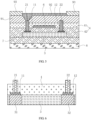
- the thin-film transistor according to some embodiments of the present disclosure as illustrated in FIG 1-FIG. 6 , comprises a first etch stopper 11, a second etch stopper 12, a source electrode 21, a drain electrode 22, an insulating layer 4, and an active layer 3.
- the first etch stopper 11 and the second etch stopper 12 are disposed over the active layer 3.
- the insulating layer 4 is disposed over, and cover, the active layer 3, the first etch stopper 11, and the second etch stopper 12.
- the insulating layer 4 is provided with a first contact via 51 and a second contact via 52.
- the source electrode 21 is electrically coupled with the active layer 3 through the first contact via 51, and the drain electrode 22 is electrically coupled with the active layer 3 through the second contact via 52.
- the first etch stopper 11 is disposed between the active layer 3 and the source electrode 21, and the second etch stopper 12 is disposed between the active layer 3 and the drain electrode 22.
- the insulating layer 4 when forming the first contact via 51 and the second contact via 52, the insulating layer 4 can be directly etched onto the first etch stopper 11 and the second etch stopper 12. The issue of under-etching can thereby be effectively solved.
- the presence of the first etch stopper 11 and the second etch stopper 12 substantially blocks the etching to the active layer 3, thereby effectively solving the issue of over-etching. As such, the production yield of thin-film transistors can thus be improved.
- the thin-film transistor according to the embodiments of the present disclosure as described above can optionally have the following features.
- the thin-film transistor according to the embodiments can be a thin-film transistor of any structure.
- the thin-film transistor can be a bottom-gate thin-film transistor, or can be a top-gate thin-film transistor.
- the insulating layer 4 can be of a single-layer structure, or can be of a double-layer structure.
- FIG 2 and FIG 4 illustrate a thin-film transistor with an insulating layer 4 having a single-layer structure, wherein the insulating layer 4 comprises an interlayer insulating layer 41.
- the thin-film transistor as such further includes a gate electrode 6 and a gate insulating layer 42.
- the gate electrode 6 is disposed over a glass substrate 8.
- the gate insulating layer 42 is disposed over the glass substrate 8 and the gate electrode 6.
- the active layer 3, the first etch stopper 11 and the second etch stopper 12 are disposed between the gate insulating layer 42 and the interlayer insulating layer 41.
- the first etch stopper 11 and the second etch stopper 12 are disposed to be closer to the interlayer insulating layer 41.
- the interlayer insulating layer 41 needs to be thoroughly etched to thereby expose the first etch stopper 11 and the second etch stopper 12 to complete the etching process to form the contact vias.
- FIG 3 and FIG 5 illustrate a thin-film transistor with an insulating layer 4 having a double-layer structure, wherein the insulating layer 4 comprises an interlayer insulating layer 41 and a gate insulating layer 42.
- a thin-film transistor as such further includes a gate electrode 6.
- a buffer layer 7 can be disposed over the glass substrate 8 prior to forming an active layer 3, and after that, the active layer 3 can be disposed over the buffer layer 7.
- the gate insulating layer 42 is disposed over the active layer 3, the first etch stopper 11, the second etch stopper 12, and the buffer layer 7.
- the interlayer insulating layer 41 is disposed over the gate insulating layer 42, and the gate electrode 6 is sandwiched between the interlayer insulating layer 41 and the gate insulating layer 42.
- the interlayer insulating layer 41 and the gate insulating layer 42 need to be etched thoroughly to thereby expose the first etch stopper 11 and the second etch stopper 12 to complete the etching process to form the contact vias.
- the buffer layer 7 can have a composition of silicon oxide and/or silicon nitride;
- the active layer 3 can have a composition of polycrystalline silicon;
- the gate insulating layer can have a composition of silicon oxide, and the interlayer insulating layer 41 can have a composition of silicon oxide or silicon nitride.
- the thickness of the gate insulating layer 42 can be around 800 ⁇ - 1200 ⁇ . If the gate electrode 6 has a composition of molybdenum, the thickness of the gate electrode 6 can be around 2000 ⁇ .
- the thickness of the interlayer insulating layer 41 can be around 1500 ⁇ . If the interlayer insulating layer 41 has a composition of silicon nitride, the thickness of the interlayer insulating layer 41 can be around 3000 ⁇ .
- FIG 4 and FIG 5 illustrate a thin-film transistor employed in an Organic Light-Emitting Diode (OLED) display panel.
- the OLED display panel further comprises a planarizing layer 91, an anode layer 92, and a pixel defining layer 93.
- the planarizing layer 91 can be disposed over the insulating layer 4, the source electrode 21, and the drain electrode 22.
- the anode layer 92 is disposed over the planarizing layer 91 and the source electrode 21.
- the pixel defining layer 93 is disposed over the planarizing layer 91 and between the anode layers 92 of neighboring pixels.
- the planarizing layer 91 can have a composition of acrylic, and can have a thickness of around 20000 ⁇ ;
- the anode layer 92 can have a composition of an indium zinc oxide or an indium tin oxide, and can have a thickness of around 1500 ⁇ .
- the pixel defining layer 93 can have a composition of polyimide, and can have a thickness of around 10000 ⁇ .
- the source electrode 21 can be of an N-layer structure, where N is an integer greater than 0.
- a first layer of the source electrode 21 can be configured to contact with, and electrically couple with, the first etch stopper 11.
- the first etch stopper 11 can have a same composition as the first layer in the source electrode 21.
- the second etch stopper 12 can have a same composition as the first etch stopper 11.
- the drain electrode 22 and the source electrode 21 can have a same composition and a same structure.
- the first etch stopper 11 and the first layer in the source electrode 21 can have a same composition.
- the second etch stopper 12 and the first layer in the drain electrode 22 can have a same composition. Such a configuration ensures that the presence of the first etch stopper 11 and the second etch stopper 12 would not reduce the electrical conductivity between the active layer 3 and the source electrode 21 and the drain electrode 22.
- N can be 1, 2 or 3. If the number of layers of the source electrode 21 is 2 or 3, neighboring layers have different compositions.
- the source electrode 21 and the drain electrode 22 can have a composition of a metal.
- the source electrode 21 and the drain electrode 22 can comprise at least one of molybdenum, titanium, and aluminum.
- the first etch stopper 11 can have a composition of a metal
- the second etch stopper 12 can have a same composition as the first etch stopper 11.
- the first etch stopper 11 can comprise molybdenum
- the second etch stopper 12 can have a same composition as the first etch stopper 11. If the first etch stopper 11 and the second etch stopper 12 both have a composition of a conductive metal, after completing the etching process to form contact vias, the portions of the first etch stopper 11 and the second etch stopper 12 that are exposed can be oxidized.
- first etch stopper 11 and the second etch stopper 12 comprise molybdenum
- the molybdenum oxides can be removed by direct cleansing using water. As such, the subsequent fabrication processes can be simplified.
- the first etch stopper 11 and the second etch stopper 12 can also comprise titanium or aluminum.
- the thicknesses of the first etch stopper 11 and the second etch stopper 12 can be between 220 ⁇ and 400 ⁇ .
- the active layer 3 can comprise low temperature poly-silicon (LTPS).
- LTPS low temperature poly-silicon
- the active layer 3 comprises low temperature poly-silicon (LTPS), as shown in FIG 6 , the active layer 3 optionally further comprises a first doping region 31 and a second doping region 32, and the first etch stopper 11 is disposed over the first doping region 31, and the second etch stopper 12 is disposed over the second doping region 32.
- LTPS low temperature poly-silicon
- the first doping region 31 and the second doping region 32 can both be heavily doped regions.
- the insulating layer 4 can be directly and thoroughly etched when the insulating layer 4 is etched to form contact vias. Because of the blocking by the first etch stopper 11 and the second etch stopper 12, the active layer 3 cannot be etched in the etching process. As such, this embodiment solves the issues of under-etching and over-etching in the etching process to form contact vias, which can thus lead to an improved production yield of thin-film transistors.
- the first etch stopper 11 has a same composition as, and is configured to contact with, the first layer in the source electrode 21.
- the first etch stopper 11 and the second etch stopper 12 are configured to have a same composition.
- the source electrode 21 and the drain electrode 22 are configured to have a same composition and a same structure. All these above configurations ensure that the presence of the first etch stopper 11 and the second etch stopper 12 would not affect the electrical conductivity between the active layer 3 and the source electrode 21 and the drain electrode 22.
- the present disclosure further provides an array substrate.
- the array substrate comprises a thin-film transistor according to any of the embodiments as described above, which thus solves the issues of under-etching and over-etching in the etching process to form contact vias and improves the yield rate of thin-film transistors.
- the first etch stopper 11 has a same composition as, and is configured to contact with, the first layer in the source electrode 21.
- the first etch stopper 11 and the second etch stopper 12 are configured to have a same composition.
- the source electrode 21 and the drain electrode 22 are configured to have a same composition and a same structure. All these above ensure that the presence of the first etch stopper 11 and the second etch stopper 12 would not affect the electrical conductivity between the active layer 3 and the source electrode 21 and the drain electrode 22.
- the array substrate according to any of the embodiments of the present disclosure as described above has a relatively high production yield, and a relatively good conductivity between the active layer 3 and the source electrode 21 and the drain electrode 22.
- the present disclosure further provides a display apparatus.
- the display apparatus comprises an array substrate according to any of embodiments as described above.
- the display apparatus solves the issues of under-etching and over-etching in the etching process to form contact vias and improves the yield rate of array substrates.
- the first etch stopper 11 has a same composition as, and is configured to contact with, the first layer in the source electrode 21.
- the first etch stopper 11 and the second etch stopper 12 are configured to have a same composition.
- the source electrode 21 and the drain electrode 22 are configured to have a same composition and a same structure. All these above ensure that the presence of the first etch stopper 11 and the second etch stopper 12 would not affect the electrical conductivity between the active layer 3 and the source electrode 21 and the drain electrode 22.
- the display apparatus according to any of the embodiments of the present disclosure as described above has a relatively high production yield, and a relatively good conductivity between the active layer 3 and the source electrode 21 and the drain electrode 22.
- the present disclosure further provides a method for manufacturing a thin-film transistor according to any of the embodiments as described above.
- the manufacturing method comprises:
- the insulating layer 4 when etching the insulating layer 4 to form the first contact via 51 and the second contact via 52, the insulating layer 4 can be directly etched through onto the first etch stopper 11 and the second etch stopper 12. The issue of under-etching can thereby be effectively solved.
- the presence of the first etch stopper 11 and the second etch stopper 12 substantially blocks the etching to the active layer 3, thereby effectively solving the issue of over-etching. As such, the production yield of thin-film transistors can thus be improved.
- the method further comprises: Performing a patterning process on the first etch stopper 11 and the second etch stopper 12 by means of a negative photoresist.
- the insulating layer 4 can be of a single-layer structure, or of a double-layer structure, or of a laminated structure.
- the manufacturing method further comprises:
- the manufacturing method further comprises: Forming an insulating layer 4 over the gate insulating layer 42.
- the insulating layer 4 formed over the active layer 3, the first etch stopper 11, and the second etch stopper 12, as well as the insulating layer 4 formed over the gate insulating layer 42, can be formed in the same step.
- the interlayer insulating layer 41 needs to be thoroughly etched to expose the first etch stopper 11 and the second etch stopper 12 so as to complete the etching process to form the contact vias.
- the insulating layer 4 comprises an interlayer insulating layer 41 and a gate insulating layer 42, and forming an insulating layer 4 over the active layer 3, the first etch stopper 11 and the second etch stopper 12 further comprises:
- the method can further comprise: Forming a gate electrode 6 over the gate insulating layer 42, as shown in FIG 19 .
- the interlayer insulating layer 41 and the gate insulating layer 42 need to be etched thoroughly to thereby expose the first etch stopper 11 and the second etch stopper 12 so as to complete the etching process to form the contact vias.
- the manufacturing method further comprises:
- the manufacturing method further comprises: Forming a gate insulating layer 42 over the buffer layer 7.
- forming a gate insulating layer 42 over the active layer 3, the first etch stopper 11, and the second etch stopper 12, and forming a gate insulating layer 42 over the buffer layer 7 as well, can be completed in a same step.
- the buffer layer 7 can have a composition of silicon oxide and/or silicon nitride
- the active layer 3 can have a composition of poly-silicon
- the gate insulating layer 42 can have a composition of silicon oxide
- the interlayer insulating layer 42 have a composition of silicon oxide or silicon nitride.
- the active layer 3 has a composition of low temperature poly-silicon, and forming an active layer 3 specifically include:
- the manufacturing method further comprises: Performing injective excitation to the active layer 3 to improve the lattice state of the low temperature poly-silicon in the active layer 3 to thereby improve the conductivity of the active layer 3.
- the gate insulating layer 42 can have a thickness between 800 ⁇ - 1200 ⁇ .
- the thickness of the gate electrode 6 can be 2000 ⁇ .
- the thickness of the interlayer insulating layer 41 can be 1500 ⁇ ;
- the thickness of the interlayer insulating layer 41 can be 3000 ⁇ .
- the manufacturing method further comprises:
- the planarizing layer 91 can have a composition of acrylic, and can have a thickness of around 20000 ⁇ .
- the anode layer 92 can have a composition of indium zinc oxide or indium tin oxide, and can have a thickness of around 1500 ⁇ .
- the pixel defining layer 93 can have a composition of polyimide, and can have a thickness of around 10000 ⁇ .
- the source electrode 21 can be of an N-layer structure, where N is an integer greater than 0.
- a first layer in the source electrode 21 can be configured to contact with, and electrically couple with, the first etch stopper 11.
- the first etch stopper 11 can have a same composition as the first layer in the source electrode 21.
- the second etch stopper 12 and the first etch stopper 11 can have a same composition.
- the drain electrode 22 and the source electrode 21 can have a same composition and a same structure.
- the first etch stopper 11 and the first layer in the source electrode 21 are configured to have a same composition
- the second etch stopper 12 and the first layer in the drain electrode 22 are configured to have a same composition.
- the number of layers of the source electrode 21 is 2 or 3, neighboring layers in the source electrode 21 have different compositions.
- the source electrode 21 and the drain electrode 22 can comprise a metal.
- the source electrode 21 and the drain electrode 22 can comprise at least one of molybdenum, titanium, and aluminum.
- the thickness of the source electrode 21 and the drain electrode 22 can be around 500 ⁇ . If the source electrode 21 and the drain electrode 22 comprise only aluminum, the thickness of the source electrode 21 and the drain electrode 22 can be around 2200 ⁇ .
- the first etch stopper 11 can comprise a metal; the second etch stopper 12 and the first etch stopper 11 can have a same composition.
- the first etch stopper 11 comprises molybdenum
- the second etch stopper 12 and the first etch stopper 11 have a same composition.
- the portions of the first etch stopper 11 and the second etch stopper 12 that are exposed can be oxidized after completion of the etching process to form contact vias.
- the oxidized substance is a water-soluble substance, and thereby the oxidized molybdenum can be directly removed by cleansing with water.
- first etch stopper 11 and the second etch stopper 12 can also comprise titanium or aluminum.
- the thicknesses of the first etch stopper 11 and the second etch stopper 12 is between 200 ⁇ and 400 ⁇ .
- the active layer 3 has a composition of low temperature poly-silicon, as shown in FIG 6 , and the active layer 3 comprises a first doping region 31 and a second doping region 32, wherein the first etch stopper 11 is disposed over the first doping region 31, the second etch stopper 12 is disposed over the second doping region 32.
- the manufacturing method can further comprise:
- the first doping region 31 and the second doping region 32 can both be heavily doped regions.
- this embodiment of the method for manufacturing a thin-film transistor by arranging a first etch stopper 11 and a second etch stopper 12 between the insulating layer 4 and the active layer 3, the insulating layer 4 can be directly and thoroughly etched when the insulating layer 4 is etched to form contact vias. Because of the blocking by the first etch stopper 11 and the second etch stopper 12, the active layer 3 cannot be etched in the etching process. As such, this embodiment of the fabrication method solves the issues of under- etching and over-etching in the etching process to form contact vias, which can lead to an improved production yield of thin-film transistors.
- the first etch stopper 11 has a same composition as, and is configured to contact with, the first layer in the source electrode 21.
- the first etch stopper 11 and the second etch stopper 12 are configured to have a same composition.
- the source electrode 21 and the drain electrode 22 are configured to have a same composition and a same structure. All these above configurations ensure that the presence of the first etch stopper 11 and the second etch stopper 12 would not affect the electrical conductivity between the active layer 3 and the source electrode 21 and the drain electrode 22.
Landscapes
- Thin Film Transistor (AREA)
- Internal Circuitry In Semiconductor Integrated Circuit Devices (AREA)
Description
- The present application claims priority to
Chinese Patent Application No. 201610189104.0 filed on March 29, 2016 - The present disclosure relates generally to display technologies, and more specifically to a thin-film transistor and its manufacturing method, an array substrate, and a display apparatus.
- Thin-film transistors are employed to produce high-end display apparatuses with high-quality display effects. Each pixel on a display panel in a display apparatus is driven to emit light by a thin-film transistor integrated in the display panel.
- At present, the manufacturing method of a thin-film transistor typically comprises the following steps:
- Forming an active layer, wherein the active layer comprises a source doping region and a drain doping region;
- Depositing an insulating layer over the active layer;
- Etching the insulating layer over the source doping region and over the drain doping region respectively to thereby expose the source doping region and the drain doping region and form two contact vias;
- Depositing a source-drain metal layer over the insulating layer and forming a source electrode and a drain electrode through a patterning process over the source-drain metal layer. Examples of manufacturing methods for TFT are provided in
CN 102280488 A , inCN103545319 A , and inUS6331467 B1 . - The conventional manufacturing method of a thin-film transistor as described above includes at least the following issues:
At present, due to the difficulty to control the etching process, issues such as over-etching and under-etching with regard to the contact vias often arise during etching of the insulating layer to form contact vias. Both the issue of over-etching and the issue of under-etching can have adverse effects to the thin-film transistors that are manufactured this way, which can ultimately lead to reduced yield of the thin-film transistors. - The invention is set out in the appended set of claims.
- To more clearly illustrate some of the embodiments of the present disclosure as described above, the following is a brief description of the drawings. The drawings in the following descriptions are only illustrative of some embodiments. For those of ordinary skill in the art, other drawings of other embodiments can become apparent based on these drawings.
-
FIG 1 is a schematic view of a structure of a thin-film transistor according to some embodiments of the present disclosure; -
FIG 2 is a schematic view of a structure of a thin-film transistor according to some embodiments of the present disclosure; -
FIG 3 is a schematic view of the structure of the thin-film transistor according to some embodiments of the present disclosure; -
FIG 4 is a schematic view of the structure of the thin-film transistor according to some embodiments of the present disclosure; -
FIG 5 is a schematic view of the structure of the thin-film transistor according to some embodiments of the present disclosure; -
FIG 6 is a schematic view of the structure of the thin-film transistor according to some embodiments of the present disclosure; -
FIGS. 7-20 are schematic views illustrating a method for manufacturing a thin-film transistor according to some embodiments of the present disclosure. - In the following, with reference to the drawings of various embodiments disclosed herein, the technical solutions of the embodiments of the present disclosure will be described in a clear and fully understandable way.
- It is obvious that the described embodiments represent merely a portion, but not all, of the embodiments of the present disclosure.
- In order to address the issues associated with current technology in fabricating thin-film transistors, the present disclosure provides a method for manufacturing a thin-film transistor and a thin-film transistor manufactured thereby.
- The method comprises: forming a first layer; forming at least one etch stopper over the first layer; forming a second layer over the first layer and the at least one etch stopper; forming at least one contact via in the second layer, such that a bottom opening of each contact via contacts with a top surface of one etch stopper; and forming at least one electrode in the at least one contact via, such that each electrode extends in one contact via respectively, and is in contact with, and electrically coupled with, the one etch stopper. The at least one etch stopper comprises a composition. The composition is capable of blocking etching to the first layer during formation of the at least one contact via in the second layer; and the composition also has one of the following characteristics: an oxidization product of the composition is readily removable by a solution; an oxidization product is conductive; or the composition is resistant to oxidization.
- By applying the method as described above, a thin-film transistor can be manufactured. The thin-film transistor comprises a first layer; at least one etch stopper, disposed over the first layer; a second layer, disposed over the first layer and the at least one etch stopper; at least one contact via, disposed in the second layer and configured such that a bottom opening of each contact via is in contact with a top surface of one etch stopper; and at least one electrode, disposed in the at least one contact via and configured such that each electrode extends in one contact via respectively, and is in contact with, and electrically coupled with, the one etch stopper.
- In the thin-film transistor, the at least one etch stopper comprises a composition. The composition is capable of blocking etching to the first layer during formation of the at least one contact via in the second layer; and the composition also has one of the following characteristics: an oxidization product of the composition is readily removable by a solution; an oxidization product is conductive; or the composition is resistant to oxidization.
- Details of some embodiments of the method and the thin-film transistor are provided below.
- In one aspect, the present disclosure provides a thin-film transistor. The thin-film transistor, according to some embodiments of the present disclosure as illustrated in
FIG 1-FIG. 6 , comprises afirst etch stopper 11, asecond etch stopper 12, asource electrode 21, adrain electrode 22, aninsulating layer 4, and anactive layer 3. - The first etch stopper 11 and the
second etch stopper 12 are disposed over theactive layer 3. Theinsulating layer 4 is disposed over, and cover, theactive layer 3, the first etch stopper 11, and the second etch stopper 12. Theinsulating layer 4 is provided with a first contact via 51 and a second contact via 52. - The
source electrode 21 is electrically coupled with theactive layer 3 through the first contact via 51, and thedrain electrode 22 is electrically coupled with theactive layer 3 through the second contact via 52. - The
first etch stopper 11 is disposed between theactive layer 3 and thesource electrode 21, and thesecond etch stopper 12 is disposed between theactive layer 3 and thedrain electrode 22. - In the thin-film transistor according to the embodiments of the present disclosure as described above, when forming the first contact via 51 and the second contact via 52, the
insulating layer 4 can be directly etched onto thefirst etch stopper 11 and thesecond etch stopper 12. The issue of under-etching can thereby be effectively solved. - On the other hand, the presence of the first etch stopper 11 and the second etch stopper 12 substantially blocks the etching to the
active layer 3, thereby effectively solving the issue of over-etching. As such, the production yield of thin-film transistors can thus be improved. - The thin-film transistor according to the embodiments of the present disclosure as described above can optionally have the following features.
- The thin-film transistor according to the embodiments can be a thin-film transistor of any structure. For example, the thin-film transistor can be a bottom-gate thin-film transistor, or can be a top-gate thin-film transistor.
- Optionally, the
insulating layer 4 can be of a single-layer structure, or can be of a double-layer structure. -
FIG 2 andFIG 4 illustrate a thin-film transistor with aninsulating layer 4 having a single-layer structure, wherein theinsulating layer 4 comprises aninterlayer insulating layer 41. The thin-film transistor as such further includes agate electrode 6 and agate insulating layer 42. - The
gate electrode 6 is disposed over aglass substrate 8. Thegate insulating layer 42 is disposed over theglass substrate 8 and thegate electrode 6. Theactive layer 3, the first etch stopper 11 and thesecond etch stopper 12 are disposed between thegate insulating layer 42 and theinterlayer insulating layer 41. The first etch stopper 11 and thesecond etch stopper 12 are disposed to be closer to theinterlayer insulating layer 41. - When the insulating
layer 4 is etched to form contact vias, theinterlayer insulating layer 41 needs to be thoroughly etched to thereby expose thefirst etch stopper 11 and the second etch stopper 12 to complete the etching process to form the contact vias. -
FIG 3 andFIG 5 illustrate a thin-film transistor with aninsulating layer 4 having a double-layer structure, wherein theinsulating layer 4 comprises aninterlayer insulating layer 41 and agate insulating layer 42. A thin-film transistor as such further includes agate electrode 6. - In order to prevent the
active layer 3 from being affected by the impurity particles in theglass substrate 8, abuffer layer 7 can be disposed over theglass substrate 8 prior to forming anactive layer 3, and after that, theactive layer 3 can be disposed over thebuffer layer 7. Thegate insulating layer 42 is disposed over theactive layer 3, thefirst etch stopper 11, thesecond etch stopper 12, and thebuffer layer 7. The interlayer insulatinglayer 41 is disposed over thegate insulating layer 42, and thegate electrode 6 is sandwiched between the interlayer insulatinglayer 41 and thegate insulating layer 42. - When the insulating
layer 4 is etched to form contact vias, theinterlayer insulating layer 41 and thegate insulating layer 42 need to be etched thoroughly to thereby expose thefirst etch stopper 11 and thesecond etch stopper 12 to complete the etching process to form the contact vias. - Optionally, the
buffer layer 7 can have a composition of silicon oxide and/or silicon nitride; theactive layer 3 can have a composition of polycrystalline silicon; the gate insulating layer can have a composition of silicon oxide, and the interlayer insulatinglayer 41 can have a composition of silicon oxide or silicon nitride. - Specifically, if the
gate insulating layer 42 has a composition of silicon oxide, the thickness of thegate insulating layer 42 can be around 800 Å- 1200 Å. If thegate electrode 6 has a composition of molybdenum, the thickness of thegate electrode 6 can be around 2000 Å. - If the
interlayer insulating layer 41 has a composition of silicon oxide, the thickness of the interlayer insulatinglayer 41 can be around 1500 Å. If theinterlayer insulating layer 41 has a composition of silicon nitride, the thickness of the interlayer insulatinglayer 41 can be around 3000 Å. -
FIG 4 andFIG 5 illustrate a thin-film transistor employed in an Organic Light-Emitting Diode (OLED) display panel. In addition to the thin-film transistor, the OLED display panel further comprises aplanarizing layer 91, ananode layer 92, and apixel defining layer 93. - The
planarizing layer 91 can be disposed over the insulatinglayer 4, thesource electrode 21, and thedrain electrode 22. Theanode layer 92 is disposed over theplanarizing layer 91 and thesource electrode 21. Thepixel defining layer 93 is disposed over theplanarizing layer 91 and between the anode layers 92 of neighboring pixels. - Optionally, the
planarizing layer 91 can have a composition of acrylic, and can have a thickness of around 20000 Å; theanode layer 92 can have a composition of an indium zinc oxide or an indium tin oxide, and can have a thickness of around 1500 Å. Thepixel defining layer 93 can have a composition of polyimide, and can have a thickness of around 10000 Å. - Optionally, the
source electrode 21 can be of an N-layer structure, where N is an integer greater than 0. A first layer of thesource electrode 21 can be configured to contact with, and electrically couple with, thefirst etch stopper 11. Thefirst etch stopper 11 can have a same composition as the first layer in thesource electrode 21. - The
second etch stopper 12 can have a same composition as thefirst etch stopper 11. Thedrain electrode 22 and thesource electrode 21 can have a same composition and a same structure. - The
first etch stopper 11 and the first layer in thesource electrode 21 can have a same composition. Thesecond etch stopper 12 and the first layer in thedrain electrode 22 can have a same composition. Such a configuration ensures that the presence of thefirst etch stopper 11 and thesecond etch stopper 12 would not reduce the electrical conductivity between theactive layer 3 and thesource electrode 21 and thedrain electrode 22. - Optionally, N can be 1, 2 or 3. If the number of layers of the
source electrode 21 is 2 or 3, neighboring layers have different compositions. - Optionally, the
source electrode 21 and thedrain electrode 22 can have a composition of a metal. - Optionally, the
source electrode 21 and thedrain electrode 22 can comprise at least one of molybdenum, titanium, and aluminum. - Optionally, the
first etch stopper 11 can have a composition of a metal, and thesecond etch stopper 12 can have a same composition as thefirst etch stopper 11. - In one preferred embodiment, the
first etch stopper 11 can comprise molybdenum, and thesecond etch stopper 12 can have a same composition as thefirst etch stopper 11. If thefirst etch stopper 11 and thesecond etch stopper 12 both have a composition of a conductive metal, after completing the etching process to form contact vias, the portions of thefirst etch stopper 11 and thesecond etch stopper 12 that are exposed can be oxidized. - If the
first etch stopper 11 and thesecond etch stopper 12 comprise molybdenum, after oxidization of the metal molybdenum, because the oxidized molybdenum (i.e. molybdenum oxide) is water soluble, the molybdenum oxides can be removed by direct cleansing using water. As such, the subsequent fabrication processes can be simplified. In addition, thefirst etch stopper 11 and thesecond etch stopper 12 can also comprise titanium or aluminum. - Optionally, the thicknesses of the
first etch stopper 11 and thesecond etch stopper 12 can be between 220 Å and 400 Å. - Optionally, the
active layer 3 can comprise low temperature poly-silicon (LTPS). - If the
active layer 3 comprises low temperature poly-silicon (LTPS), as shown inFIG 6 , theactive layer 3 optionally further comprises afirst doping region 31 and asecond doping region 32, and thefirst etch stopper 11 is disposed over thefirst doping region 31, and thesecond etch stopper 12 is disposed over thesecond doping region 32. - Optionally, the
first doping region 31 and thesecond doping region 32 can both be heavily doped regions. - In this embodiment of the thin-film transistor, by arranging a
first etch stopper 11 and asecond etch stopper 12 between the insulatinglayer 4 and theactive layer 3, the insulatinglayer 4 can be directly and thoroughly etched when the insulatinglayer 4 is etched to form contact vias. Because of the blocking by thefirst etch stopper 11 and thesecond etch stopper 12, theactive layer 3 cannot be etched in the etching process. As such, this embodiment solves the issues of under-etching and over-etching in the etching process to form contact vias, which can thus lead to an improved production yield of thin-film transistors. - Additionally, the
first etch stopper 11 has a same composition as, and is configured to contact with, the first layer in thesource electrode 21. Thefirst etch stopper 11 and thesecond etch stopper 12 are configured to have a same composition. Thesource electrode 21 and thedrain electrode 22 are configured to have a same composition and a same structure. All these above configurations ensure that the presence of thefirst etch stopper 11 and thesecond etch stopper 12 would not affect the electrical conductivity between theactive layer 3 and thesource electrode 21 and thedrain electrode 22. - In a second aspect, the present disclosure further provides an array substrate. The array substrate comprises a thin-film transistor according to any of the embodiments as described above, which thus solves the issues of under-etching and over-etching in the etching process to form contact vias and improves the yield rate of thin-film transistors.
- Additionally, the
first etch stopper 11 has a same composition as, and is configured to contact with, the first layer in thesource electrode 21. Thefirst etch stopper 11 and thesecond etch stopper 12 are configured to have a same composition. Thesource electrode 21 and thedrain electrode 22 are configured to have a same composition and a same structure. All these above ensure that the presence of thefirst etch stopper 11 and thesecond etch stopper 12 would not affect the electrical conductivity between theactive layer 3 and thesource electrode 21 and thedrain electrode 22. - As such, the array substrate according to any of the embodiments of the present disclosure as described above has a relatively high production yield, and a relatively good conductivity between the
active layer 3 and thesource electrode 21 and thedrain electrode 22. - In a third aspect, the present disclosure further provides a display apparatus. The display apparatus comprises an array substrate according to any of embodiments as described above.
- The display apparatus as such solves the issues of under-etching and over-etching in the etching process to form contact vias and improves the yield rate of array substrates.
- Additionally, the
first etch stopper 11 has a same composition as, and is configured to contact with, the first layer in thesource electrode 21. Thefirst etch stopper 11 and thesecond etch stopper 12 are configured to have a same composition. Thesource electrode 21 and thedrain electrode 22 are configured to have a same composition and a same structure. All these above ensure that the presence of thefirst etch stopper 11 and thesecond etch stopper 12 would not affect the electrical conductivity between theactive layer 3 and thesource electrode 21 and thedrain electrode 22. - As such, the display apparatus according to any of the embodiments of the present disclosure as described above has a relatively high production yield, and a relatively good conductivity between the
active layer 3 and thesource electrode 21 and thedrain electrode 22. - In a fourth aspect, the present disclosure further provides a method for manufacturing a thin-film transistor according to any of the embodiments as described above. The manufacturing method comprises:
- Forming an
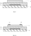
active layer 3, as shown inFIG 9 ; - Forming a
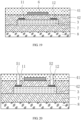
first etch stopper 11 and asecond etch stopper 12 over theactive layer 3, as shown inFIG 10 ; - Forming an insulating
layer 4 over theactive layer 3, thefirst etch stopper 11, and thesecond etch stopper 12, as shown inFIG 11 ; - Etching the insulating
layer 4 at positions corresponding to thefirst etch stopper 11 and thesecond etch stopper 12 to form a first contact via 51 and a second contact via 52, wherein thefirst etch stopper 11 and thesecond etch stopper 12 are exposed, as shown inFIG 12 ; - Forming a
source electrode 21 and adrain electrode 22 in the first contract via 51 and the second contact via 52 respectively, as shown inFIG 1 - FIG 6 . - In the embodiment, when etching the insulating
layer 4 to form the first contact via 51 and the second contact via 52, the insulatinglayer 4 can be directly etched through onto thefirst etch stopper 11 and thesecond etch stopper 12. The issue of under-etching can thereby be effectively solved. - On the other hand, the presence of the
first etch stopper 11 and thesecond etch stopper 12 substantially blocks the etching to theactive layer 3, thereby effectively solving the issue of over-etching. As such, the production yield of thin-film transistors can thus be improved. - Optionally, prior to forming a
source electrode 21 and adrain electrode 22 in the first contract via 51 and the second contact via 51, the method further comprises:
Performing a patterning process on thefirst etch stopper 11 and thesecond etch stopper 12 by means of a negative photoresist. - Optionally, the insulating
layer 4 can be of a single-layer structure, or of a double-layer structure, or of a laminated structure. - Specifically, if the insulating
layer 4 is of a single-layer structure, the insulatinglayer 4 comprises an interlayer insulatinglayer 41, and the manufacturing method further comprises: - Forming a
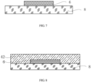
gate electrode 6 over aglass substrate 8, as shown inFIG7 ; - Forming a
gate insulating layer 42 over thegate electrode 6 and theglass substrate 8, as shown inFIG 8 ; and - Forming an
active layer 3 over thegate insulating layer 42, as shown inFIG 9 . - If the insulating
layer 4 is of a single-layer structure, at the same time of forming the insulatinglayer 4 over theactive layer 3, thefirst etch stopper 11, and thesecond etch stopper 12, the manufacturing method further comprises:
Forming an insulatinglayer 4 over thegate insulating layer 42. - Specifically, as shown in
FIG 11 , if the insulatinglayer 4 is of a single layer structure, the insulatinglayer 4 formed over theactive layer 3, thefirst etch stopper 11, and thesecond etch stopper 12, as well as the insulatinglayer 4 formed over thegate insulating layer 42, can be formed in the same step. - As shown in
FIG 2 andFIG 12 , when etching the insulatinglayer 4 to form the contact vias, theinterlayer insulating layer 41 needs to be thoroughly etched to expose thefirst etch stopper 11 and thesecond etch stopper 12 so as to complete the etching process to form the contact vias. - Specifically, if the insulating
layer 4 is of a double-layer structure, the insulatinglayer 4 comprises an interlayer insulatinglayer 41 and agate insulating layer 42, and forming an insulatinglayer 4 over theactive layer 3, thefirst etch stopper 11 and thesecond etch stopper 12 further comprises: - Forming a
gate insulating layer 42 over the active layer 2, thefirst etch stopper 11 and thesecond etch stopper 12, as shown inFIG 18 ; and - Forming an
interlayer insulating layer 41 over thegate insulating layer 42, as shown inFIG 19 . - In this embodiment, prior to forming an interlayer insulating
layer 41 over thegate insulating layer 42, the method can further comprise:
Forming agate electrode 6 over thegate insulating layer 42, as shown inFIG 19 . - As shown in
FIG 3 ,FIG 5 andFIG 20 , when etching the insulatinglayer 4 to form contact vias, theinterlayer insulating layer 41 and thegate insulating layer 42 need to be etched thoroughly to thereby expose thefirst etch stopper 11 and thesecond etch stopper 12 so as to complete the etching process to form the contact vias. - Optionally, if the insulating
layer 4 is of a double-layer structure, the manufacturing method further comprises: - Forming a
buffer layer 7 over aglass substrate 8, as shown inFIG 15 ; and - Forming an
active layer 3 over thebuffer layer 7, as shown inFIG 16 . - If the insulating
layer 4 is a double-layer structure, at the same time of forming thegate insulating layer 42 over theactive layer 3, thefirst etch stopper 11 and thesecond etch stopper 12, the manufacturing method further comprises:
Forming agate insulating layer 42 over thebuffer layer 7. - Specifically, if the insulating
layer 4 is of a double-layer structure, forming agate insulating layer 42 over theactive layer 3, thefirst etch stopper 11, and thesecond etch stopper 12, and forming agate insulating layer 42 over thebuffer layer 7 as well, can be completed in a same step. - Optionally, the
buffer layer 7 can have a composition of silicon oxide and/or silicon nitride, theactive layer 3 can have a composition of poly-silicon, thegate insulating layer 42 can have a composition of silicon oxide, and the interlayer insulatinglayer 42 have a composition of silicon oxide or silicon nitride. - According to the invention, the
active layer 3 has a composition of low temperature poly-silicon, and forming anactive layer 3 specifically include: - Forming an amorphous silicon layer;
- Performing annealing to the amorphous silicon layer;
- Performing an excimer laser annealing process to the amorphous silicon layer after annealing, wherein the amorphous silicon layer is crystallized and the amorphous silicon layer is transformed into a low temperature poly-silicon layer;
- Exposing and developing the low temperature poly-silicon layer by means of a positive photoresist to thereby form a patterned
active layer 3, wherein the thickness of the positive photoresist is between 2 µm and 3 µm. - Specifically, if the
active layer 3 has a composition of low temperature poly-silicon, prior to etching the insulatinglayer 4 at positions corresponding to thefirst etch stopper 11 and thesecond etch stopper 12 to form the first contact via 51 and the second contact via 51, the manufacturing method further comprises:
Performing injective excitation to theactive layer 3 to improve the lattice state of the low temperature poly-silicon in theactive layer 3 to thereby improve the conductivity of theactive layer 3. - Specifically, if the insulating
layer 4 is of a single-layer structure or a double layer-structure and thegate insulating layer 42 has a composition of silicon oxide, thegate insulating layer 42 can have a thickness between 800 Å - 1200 Å. - If the
gate electrode 6 comprises molybdenum, the thickness of thegate electrode 6 can be 2000 Å. - If the
interlayer insulating layer 41 comprises silicon oxide, the thickness of the interlayer insulatinglayer 41 can be 1500 Å; - If the
interlayer insulating layer 41 comprises silicon nitride, the thickness of the interlayer insulatinglayer 41 can be 3000 Å. - Optionally, when the thin-film transistor is employed for OLED back panel, the manufacturing method further comprises:
- Forming a
planarizing layer 91 over the insulatinglayer 4, thesource electrode 21, and thedrain electrode 22, as shown inFIG 13 ; - Forming an
anode layer 92 over theplanarizing layer 91 and thesource electrode 21, as shown inFIG 14 ; - Forming a
pixel defining layer 93 over theplanarizing layer 91 such that thepixel defining layer 93 is disposed between the anode layers 92 of neighboring pixel units. - Optionally, the
planarizing layer 91 can have a composition of acrylic, and can have a thickness of around 20000 Å. Theanode layer 92 can have a composition of indium zinc oxide or indium tin oxide, and can have a thickness of around 1500 Å. Thepixel defining layer 93 can have a composition of polyimide, and can have a thickness of around 10000 Å. - Optionally, the
source electrode 21 can be of an N-layer structure, where N is an integer greater than 0. A first layer in thesource electrode 21 can be configured to contact with, and electrically couple with, thefirst etch stopper 11. Thefirst etch stopper 11 can have a same composition as the first layer in thesource electrode 21. - The
second etch stopper 12 and thefirst etch stopper 11 can have a same composition. Thedrain electrode 22 and thesource electrode 21 can have a same composition and a same structure. - The
first etch stopper 11 and the first layer in thesource electrode 21 are configured to have a same composition, and thesecond etch stopper 12 and the first layer in thedrain electrode 22 are configured to have a same composition. Such a configuration ensures that the existence of thefirst etch stopper 11 and thesecond etch stopper 12 would not reduce the electrical conductivity between theactive layer 3 and thesource electrode 21 and thedrain electrode 22. - According to the invention, if the number of layers of the
source electrode 21 is 2 or 3, neighboring layers in thesource electrode 21 have different compositions. - Optionally, the
source electrode 21 and thedrain electrode 22 can comprise a metal. To be more specific, thesource electrode 21 and thedrain electrode 22 can comprise at least one of molybdenum, titanium, and aluminum. - Optionally, if the
source electrode 21 and thedrain electrode 22 comprise only molybdenum, the thickness of thesource electrode 21 and thedrain electrode 22 can be around 500 Å. If thesource electrode 21 and thedrain electrode 22 comprise only aluminum, the thickness of thesource electrode 21 and thedrain electrode 22 can be around 2200 Å. - Optionally, the
first etch stopper 11 can comprise a metal; thesecond etch stopper 12 and thefirst etch stopper 11 can have a same composition. - According to the invention, the
first etch stopper 11 comprises molybdenum, thesecond etch stopper 12 and thefirst etch stopper 11 have a same composition. Under a circumstance where thefirst etch stopper 11 and thesecond etch stopper 12 both comprise a conductive metal material, the portions of thefirst etch stopper 11 and thesecond etch stopper 12 that are exposed can be oxidized after completion of the etching process to form contact vias. - Under a circumstance where the
first etch stopper 11 and thesecond etch stopper 12 both comprise molybdenum, after the metal molybdenum is oxidized, the oxidized substance is a water-soluble substance, and thereby the oxidized molybdenum can be directly removed by cleansing with water. - As such, the subsequent processes during manufacturing can be simplified if molybdenum is employed as the material of the etch stoppers. In addition, the
first etch stopper 11 and thesecond etch stopper 12 can also comprise titanium or aluminum. - According to the invention, the thicknesses of the
first etch stopper 11 and thesecond etch stopper 12 is between 200 Å and 400 Å. - According to the invention, the
active layer 3 has a composition of low temperature poly-silicon, as shown inFIG 6 , and theactive layer 3 comprises afirst doping region 31 and asecond doping region 32, wherein thefirst etch stopper 11 is disposed over thefirst doping region 31, thesecond etch stopper 12 is disposed over thesecond doping region 32. - Specifically, before forming the
first etch stopper 11 and thesecond etch stopper 12 over theactive layer 3, the manufacturing method can further comprise: - Performing doping to the
active layer 3 to thereby form afirst doping region 31 and asecond doping region 32 respectively in theactive layer 3. - Optionally, the
first doping region 31 and thesecond doping region 32 can both be heavily doped regions. - In this embodiment of the method for manufacturing a thin-film transistor, by arranging a
first etch stopper 11 and asecond etch stopper 12 between the insulatinglayer 4 and theactive layer 3, the insulatinglayer 4 can be directly and thoroughly etched when the insulatinglayer 4 is etched to form contact vias. Because of the blocking by thefirst etch stopper 11 and thesecond etch stopper 12, theactive layer 3 cannot be etched in the etching process. As such, this embodiment of the fabrication method solves the issues of under- etching and over-etching in the etching process to form contact vias, which can lead to an improved production yield of thin-film transistors. - Additionally, the
first etch stopper 11 has a same composition as, and is configured to contact with, the first layer in thesource electrode 21. Thefirst etch stopper 11 and thesecond etch stopper 12 are configured to have a same composition. Thesource electrode 21 and thedrain electrode 22 are configured to have a same composition and a same structure. All these above configurations ensure that the presence of thefirst etch stopper 11 and thesecond etch stopper 12 would not affect the electrical conductivity between theactive layer 3 and thesource electrode 21 and thedrain electrode 22. - Although specific embodiments have been described above in detail, the description is merely for purposes of illustration.
Claims (5)
- A method for manufacturing a thin-film transistor, comprising:forming an active layer (3) using low temperature poly-silicon (LTPS), wherein the active layer (3) comprises a first doping region (31) and a second doping region (32);;forming a first etch stopper (11) and a second etch stopper (12) respectively over the first doping region (31) and the second doping region (32), thicknesses of the first etch stopper (11) and the second etch stopper (12) each being between 200 Å and 400 Å ;forming a second layer over the active layer and the at least one etch stopper (11,12);forming at least one contact via (51, 52) in the second layer, such that a bottom opening of each contact via (51, 52) contacts with a top surface of one etch stopper (11,12); andforming at least one electrode (21,22) in the at least one contact via (51, 52), such that each electrode (21,22) extends in one contact via (51, 52) respectively, and is in contact with, and electrically coupled with, the one etch stopper (11,12);wherein:
the at least one etch stopper (11,12) comprises a composition capable of blocking etching to the active layer during formation of the at least one contact via (51, 52) in the second layer; and
whose oxidization product is removable by a solution, the composition comprising molybdenum;wherein,each electrode is formed into an N-layer structure, where N is an integer greater than 1;neighboring layers of each electrode are made of different compositions ;a contact layer of each electrode, in contact with and electrically coupled to, one etch stopper (11,12), is made of a same composition as the one etch stopper (11,12), and whereforming the active layer (3) using low temperature poly-silicon (LTPS) further comprises: performing injective excitation on the active layer (3) to improve the lattice state of the low temperature poly-silicon in the active layer (3) to thereby improve the conductivity of the active layer (3). - The method according to Claim 1, wherein:the second layer is an insulating layer (4);the at least one contact via (51, 52) comprises a first contact via (51) and a second contact via (52);the at least one electrode (21,22) comprises a source electrode (21) and a drain electrode (22), disposed in the first contact via (51) and the second contact via (52) respectively, and electrically coupled with the first etch stopper (11) and the second etch stopper (12) respectively.
- The method according to Claim 2, wherein:the method further comprises, prior to forming a first layer:forming a gate electrode (6) over a substrate (8); andforming a gate insulating layer (42) over the gate electrode (6) and the substrate (8);forming a first layer comprises:
forming an active layer (3) over the gate insulating layer (42); andforming a second layer over the first layer and the at least one etch stopper (11,12) comprises:
forming an insulating layer (4) over the gate insulating layer (42), the active layer (3), the first etch stopper (11), and the second etch stopper (12). - The method according to Claim 2, wherein:the method further comprises, between forming a second layer over the first layer and the at least one etch stopper (11,12) and forming at least one contact via (51, 52) in the second layer:forming a gate electrode (6) over the insulating layer (4); andforming a gate insulating layer (42) over the gate electrode (6) and the insulating layer (4);
andforming at least one contact via (51, 52) in the second layer comprises:
forming a first contact via (51) and a second contact via (52) through the insulating layer (4) and the gate insulating layer (42),the method further comprises, prior to forming a first layer:
forming a buffer layer (7) over a substrate (8);forming a first layer comprises:
forming an active layer (3) over the buffer layer (7); andforming a second layer over the first layer and the at least one etch stopper (11,12) comprises:
forming an insulating layer (4) over the buffer layer (7), the active layer (3), the first etch stopper (11), and the second etch stopper (12). - The method according to Claim 2, further comprising:forming a planarizing layer (91) over the insulating layer (4), the source electrode (21) and the drain electrode (22), wherein the planarizing layer (91) is provided with a third contact via, disposed over the source electrode (21); andforming an anode layer (92) over the planarizing layer (91), wherein the anode layer (92) is configured to electrically couple with the source electrode (21) through the third contact via.
Applications Claiming Priority (2)
| Application Number | Priority Date | Filing Date | Title |
|---|---|---|---|
| CN201610189104.0A CN105609567A (en) | 2016-03-29 | 2016-03-29 | Thin film transistor and manufacturing method, array substrate and display device |
| PCT/CN2016/107172 WO2017166833A1 (en) | 2016-03-29 | 2016-11-25 | Thin-film transistor and manufacturing method thereof, array substrate, and display apparatus |
Publications (3)
| Publication Number | Publication Date |
|---|---|
| EP3437140A1 EP3437140A1 (en) | 2019-02-06 |
| EP3437140A4 EP3437140A4 (en) | 2019-11-13 |
| EP3437140B1 true EP3437140B1 (en) | 2025-01-01 |
Family
ID=55989334
Family Applications (1)
| Application Number | Title | Priority Date | Filing Date |
|---|---|---|---|
| EP16869379.4A Active EP3437140B1 (en) | 2016-03-29 | 2016-11-25 | Thin-film transistor and manufacturing method thereof, array substrate, and display apparatus |
Country Status (4)
| Country | Link |
|---|---|
| US (1) | US10615282B2 (en) |
| EP (1) | EP3437140B1 (en) |
| CN (1) | CN105609567A (en) |
| WO (1) | WO2017166833A1 (en) |
Families Citing this family (8)
| Publication number | Priority date | Publication date | Assignee | Title |
|---|---|---|---|---|
| CN105609567A (en) * | 2016-03-29 | 2016-05-25 | 京东方科技集团股份有限公司 | Thin film transistor and manufacturing method, array substrate and display device |
| CN107316874B (en) * | 2017-07-28 | 2020-03-10 | 武汉华星光电技术有限公司 | Array substrate, manufacturing method thereof and display device |
| CN109273409B (en) | 2018-08-24 | 2022-01-18 | 京东方科技集团股份有限公司 | Display panel, manufacturing method thereof and display device |
| EP3640845A4 (en) * | 2018-09-06 | 2020-09-02 | Shenzhen Goodix Technology Co., Ltd. | Optical image collection unit, optical image collection system and electronic device |
| KR102951418B1 (en) * | 2020-08-10 | 2026-04-10 | 삼성디스플레이 주식회사 | Display apparatus |
| KR102945393B1 (en) * | 2020-08-18 | 2026-03-31 | 삼성디스플레이 주식회사 | Display device and method for manufacturing the same |
| KR102746684B1 (en) | 2020-09-14 | 2024-12-27 | 삼성디스플레이 주식회사 | Display device and method of manufacturing the same |
| CN115000093B (en) * | 2022-06-01 | 2025-05-30 | 广州华星光电技术有限公司 | Array substrate and manufacturing method thereof, and display panel |
Citations (1)
| Publication number | Priority date | Publication date | Assignee | Title |
|---|---|---|---|---|
| US6331476B1 (en) * | 1998-05-26 | 2001-12-18 | Mausushita Electric Industrial Co., Ltd. | Thin film transistor and producing method thereof |
Family Cites Families (16)
| Publication number | Priority date | Publication date | Assignee | Title |
|---|---|---|---|---|
| KR100439345B1 (en) * | 2000-10-31 | 2004-07-07 | 피티플러스(주) | Thin film transistor including a polycrystalline active layer and method making same |
| KR101108369B1 (en) * | 2004-12-31 | 2012-01-30 | 엘지디스플레이 주식회사 | Array substrate for polysilicon liquid crystal display device and manufacturing method thereof |
| US20080191207A1 (en) * | 2007-02-08 | 2008-08-14 | Mitsubishi Electric Corporation | Thin film transistor device, method of manufacturing the same, and display apparatus |
| KR101108175B1 (en) * | 2010-06-09 | 2012-01-31 | 삼성모바일디스플레이주식회사 | Thin film transistor, array substrate for display device comprising same, and manufacturing method thereof |
| KR101764902B1 (en) * | 2010-12-06 | 2017-08-14 | 엘지디스플레이 주식회사 | Thin film Transistor substrate and method for manufacturing the same |
| KR101841770B1 (en) * | 2011-09-02 | 2018-03-26 | 엘지디스플레이 주식회사 | Oxide Thin Film Transistor Flat Display Device and Method for fabricating thereof |
| US8728861B2 (en) * | 2011-10-12 | 2014-05-20 | The United States Of America As Represented By The Secretary Of The Air Force | Fabrication method for ZnO thin film transistors using etch-stop layer |
| CN102646699B (en) * | 2012-01-13 | 2014-12-10 | 京东方科技集团股份有限公司 | Oxide TFT (thin film transistor) and manufacturing method thereof |
| CN102790096A (en) * | 2012-07-20 | 2012-11-21 | 京东方科技集团股份有限公司 | Film transistor as well as manufacturing method thereof, array substrate and display equipment |
| CN103258745A (en) * | 2013-04-17 | 2013-08-21 | 京东方科技集团股份有限公司 | Thin film transistor, manufacturing method of thin film transistor, array substrate and display device |
| KR101619158B1 (en) * | 2013-04-30 | 2016-05-10 | 엘지디스플레이 주식회사 | Thin Film Transistor Substrate and Organic Light Emitting Device Using That Same |
| KR102130139B1 (en) * | 2013-07-30 | 2020-07-03 | 엘지디스플레이 주식회사 | Organic Light Emitting Diode Display Having Thin Film Transistor Substrate Using Oxide Semiconductor And Method For Manufacturing The Same |
| CN103545319A (en) * | 2013-11-08 | 2014-01-29 | 京东方科技集团股份有限公司 | Low-temperature polycrystalline silicon thin film transistor array substrate, manufacturing method thereof and display device |
| KR20150073297A (en) * | 2013-12-20 | 2015-07-01 | 삼성디스플레이 주식회사 | Thin film transistor, display substrate having the same and method of manufacturing a display substrate |
| CN104867985A (en) * | 2015-05-18 | 2015-08-26 | 京东方科技集团股份有限公司 | Thin film transistor, preparation method thereof, array substrate and display apparatus |
| CN105609567A (en) * | 2016-03-29 | 2016-05-25 | 京东方科技集团股份有限公司 | Thin film transistor and manufacturing method, array substrate and display device |
-
2016
- 2016-03-29 CN CN201610189104.0A patent/CN105609567A/en active Pending
- 2016-11-25 WO PCT/CN2016/107172 patent/WO2017166833A1/en not_active Ceased
- 2016-11-25 US US15/534,467 patent/US10615282B2/en active Active
- 2016-11-25 EP EP16869379.4A patent/EP3437140B1/en active Active
Patent Citations (1)
| Publication number | Priority date | Publication date | Assignee | Title |
|---|---|---|---|---|
| US6331476B1 (en) * | 1998-05-26 | 2001-12-18 | Mausushita Electric Industrial Co., Ltd. | Thin film transistor and producing method thereof |
Also Published As
| Publication number | Publication date |
|---|---|
| US20190027612A1 (en) | 2019-01-24 |
| EP3437140A4 (en) | 2019-11-13 |
| US10615282B2 (en) | 2020-04-07 |
| EP3437140A1 (en) | 2019-02-06 |
| CN105609567A (en) | 2016-05-25 |
| WO2017166833A1 (en) | 2017-10-05 |
Similar Documents
| Publication | Publication Date | Title |
|---|---|---|
| US8748897B2 (en) | Array substrate for organic electroluminescent display device | |
| US10615282B2 (en) | Thin-film transistor and manufacturing method thereof, array substrate, and display apparatus | |
| US9478562B2 (en) | Array substrate and manufacturing method thereof, display device, thin film transistor and manufacturing method thereof | |
| CN104078424B (en) | Low-temperature poly-silicon TFT array substrate, manufacturing method thereof and display device | |
| CN107275350B (en) | Array substrate, method for making the same, and display device | |
| US8883579B2 (en) | Array substrate for organic electroluminescent display device and method of fabricating the same | |
| CN104362125B (en) | Array base palte and preparation method thereof, display device | |
| CN104282769B (en) | Thin film transistor manufacturing method, and manufacturing method of array substrate | |
| US6617203B2 (en) | Flat panel display device and method of manufacturing the same | |
| WO2016026246A1 (en) | Thin film transistor and manufacturing method thereof, array substrate and manufacturing method thereof and display device | |
| EP2728620B1 (en) | Array substrate, manufacturing method thereof and display device | |
| US20110303923A1 (en) | Tft, array substrate for display apparatus including tft, and methods of manufacturing tft and array substrate | |
| TW201714008A (en) | Array substrate, display device and array substrate manufacturing method array substrate | |
| CN105304500B (en) | N-type TFT preparation method | |
| CN104240633A (en) | Thin film transistor and active matrix organic light emitting diode assembly and manufacturing method thereof | |
| US20150295094A1 (en) | Thin film transistor, manufacturing method thereof, array substrate and display device | |
| WO2017028461A1 (en) | Preparation method for thin film transistor, preparation method for array substrate, array substrate, and display apparatus | |
| US12261227B2 (en) | Thin film transistor, display substrate and display device with reduced leakage current | |
| WO2018214732A1 (en) | Array substrate and manufacturing method thereof, and display device | |
| US9159773B2 (en) | Thin film transistor and active matrix organic light emitting diode assembly | |
| WO2016123979A1 (en) | Thin-film transistor and manufacturing method therefor, array substrate and display device | |
| WO2020037850A1 (en) | Array substrate and manufacturing method therefor, and display panel | |
| KR20110058356A (en) | Array substrate and its manufacturing method | |
| CN117476691A (en) | Array substrate and manufacturing method thereof, display panel | |
| US20210335850A1 (en) | Display panel and manufacturing method thereof, and electronic equipment |
Legal Events
| Date | Code | Title | Description |
|---|---|---|---|
| STAA | Information on the status of an ep patent application or granted ep patent |
Free format text: STATUS: UNKNOWN |
|
| STAA | Information on the status of an ep patent application or granted ep patent |
Free format text: STATUS: THE INTERNATIONAL PUBLICATION HAS BEEN MADE |
|
| PUAI | Public reference made under article 153(3) epc to a published international application that has entered the european phase |
Free format text: ORIGINAL CODE: 0009012 |
|
| STAA | Information on the status of an ep patent application or granted ep patent |
Free format text: STATUS: REQUEST FOR EXAMINATION WAS MADE |
|
| 17P | Request for examination filed |
Effective date: 20170608 |
|
| AK | Designated contracting states |
Kind code of ref document: A1 Designated state(s): AL AT BE BG CH CY CZ DE DK EE ES FI FR GB GR HR HU IE IS IT LI LT LU LV MC MK MT NL NO PL PT RO RS SE SI SK SM TR |
|
| AX | Request for extension of the european patent |
Extension state: BA ME |
|
| DAV | Request for validation of the european patent (deleted) | ||
| DAX | Request for extension of the european patent (deleted) | ||
| A4 | Supplementary search report drawn up and despatched |
Effective date: 20191014 |
|
| RIC1 | Information provided on ipc code assigned before grant |
Ipc: H01L 29/417 20060101ALI20191008BHEP Ipc: H01L 29/66 20060101ALI20191008BHEP Ipc: H01L 27/12 20060101ALI20191008BHEP Ipc: H01L 29/786 20060101AFI20191008BHEP Ipc: H01L 29/45 20060101ALI20191008BHEP |
|
| STAA | Information on the status of an ep patent application or granted ep patent |
Free format text: STATUS: EXAMINATION IS IN PROGRESS |
|
| 17Q | First examination report despatched |
Effective date: 20200819 |
|
| GRAP | Despatch of communication of intention to grant a patent |
Free format text: ORIGINAL CODE: EPIDOSNIGR1 |
|
| STAA | Information on the status of an ep patent application or granted ep patent |
Free format text: STATUS: GRANT OF PATENT IS INTENDED |
|
| INTG | Intention to grant announced |
Effective date: 20241009 |
|
| GRAS | Grant fee paid |
Free format text: ORIGINAL CODE: EPIDOSNIGR3 |
|
| GRAA | (expected) grant |
Free format text: ORIGINAL CODE: 0009210 |
|
| STAA | Information on the status of an ep patent application or granted ep patent |
Free format text: STATUS: THE PATENT HAS BEEN GRANTED |
|
| AK | Designated contracting states |
Kind code of ref document: B1 Designated state(s): AL AT BE BG CH CY CZ DE DK EE ES FI FR GB GR HR HU IE IS IT LI LT LU LV MC MK MT NL NO PL PT RO RS SE SI SK SM TR |
|
| REG | Reference to a national code |
Ref country code: GB Ref legal event code: FG4D |
|
| REG | Reference to a national code |
Ref country code: CH Ref legal event code: EP |
|
| REG | Reference to a national code |
Ref country code: DE Ref legal event code: R096 Ref document number: 602016090843 Country of ref document: DE |
|
| REG | Reference to a national code |
Ref country code: IE Ref legal event code: FG4D |
|
| REG | Reference to a national code |
Ref country code: LT Ref legal event code: MG9D |
|
| REG | Reference to a national code |
Ref country code: NL Ref legal event code: MP Effective date: 20250101 |
|
| REG | Reference to a national code |
Ref country code: AT Ref legal event code: MK05 Ref document number: 1757218 Country of ref document: AT Kind code of ref document: T Effective date: 20250101 |
|
| PG25 | Lapsed in a contracting state [announced via postgrant information from national office to epo] |
Ref country code: NL Free format text: LAPSE BECAUSE OF FAILURE TO SUBMIT A TRANSLATION OF THE DESCRIPTION OR TO PAY THE FEE WITHIN THE PRESCRIBED TIME-LIMIT Effective date: 20250101 |
|
| PG25 | Lapsed in a contracting state [announced via postgrant information from national office to epo] |
Ref country code: FI Free format text: LAPSE BECAUSE OF FAILURE TO SUBMIT A TRANSLATION OF THE DESCRIPTION OR TO PAY THE FEE WITHIN THE PRESCRIBED TIME-LIMIT Effective date: 20250101 |
|
| PG25 | Lapsed in a contracting state [announced via postgrant information from national office to epo] |
Ref country code: PL Free format text: LAPSE BECAUSE OF FAILURE TO SUBMIT A TRANSLATION OF THE DESCRIPTION OR TO PAY THE FEE WITHIN THE PRESCRIBED TIME-LIMIT Effective date: 20250101 |
|
| PG25 | Lapsed in a contracting state [announced via postgrant information from national office to epo] |
Ref country code: ES Free format text: LAPSE BECAUSE OF FAILURE TO SUBMIT A TRANSLATION OF THE DESCRIPTION OR TO PAY THE FEE WITHIN THE PRESCRIBED TIME-LIMIT Effective date: 20250101 |
|
| PG25 | Lapsed in a contracting state [announced via postgrant information from national office to epo] |
Ref country code: IS Free format text: LAPSE BECAUSE OF FAILURE TO SUBMIT A TRANSLATION OF THE DESCRIPTION OR TO PAY THE FEE WITHIN THE PRESCRIBED TIME-LIMIT Effective date: 20250501 Ref country code: NO Free format text: LAPSE BECAUSE OF FAILURE TO SUBMIT A TRANSLATION OF THE DESCRIPTION OR TO PAY THE FEE WITHIN THE PRESCRIBED TIME-LIMIT Effective date: 20250401 |
|
| PG25 | Lapsed in a contracting state [announced via postgrant information from national office to epo] |
Ref country code: HR Free format text: LAPSE BECAUSE OF FAILURE TO SUBMIT A TRANSLATION OF THE DESCRIPTION OR TO PAY THE FEE WITHIN THE PRESCRIBED TIME-LIMIT Effective date: 20250101 |
|
| PG25 | Lapsed in a contracting state [announced via postgrant information from national office to epo] |
Ref country code: LV Free format text: LAPSE BECAUSE OF FAILURE TO SUBMIT A TRANSLATION OF THE DESCRIPTION OR TO PAY THE FEE WITHIN THE PRESCRIBED TIME-LIMIT Effective date: 20250101 Ref country code: PT Free format text: LAPSE BECAUSE OF FAILURE TO SUBMIT A TRANSLATION OF THE DESCRIPTION OR TO PAY THE FEE WITHIN THE PRESCRIBED TIME-LIMIT Effective date: 20250502 |
|
| PG25 | Lapsed in a contracting state [announced via postgrant information from national office to epo] |
Ref country code: BG Free format text: LAPSE BECAUSE OF FAILURE TO SUBMIT A TRANSLATION OF THE DESCRIPTION OR TO PAY THE FEE WITHIN THE PRESCRIBED TIME-LIMIT Effective date: 20250101 Ref country code: GR Free format text: LAPSE BECAUSE OF FAILURE TO SUBMIT A TRANSLATION OF THE DESCRIPTION OR TO PAY THE FEE WITHIN THE PRESCRIBED TIME-LIMIT Effective date: 20250402 |
|
| PG25 | Lapsed in a contracting state [announced via postgrant information from national office to epo] |
Ref country code: AT Free format text: LAPSE BECAUSE OF FAILURE TO SUBMIT A TRANSLATION OF THE DESCRIPTION OR TO PAY THE FEE WITHIN THE PRESCRIBED TIME-LIMIT Effective date: 20250101 |
|
| PG25 | Lapsed in a contracting state [announced via postgrant information from national office to epo] |
Ref country code: CZ Free format text: LAPSE BECAUSE OF FAILURE TO SUBMIT A TRANSLATION OF THE DESCRIPTION OR TO PAY THE FEE WITHIN THE PRESCRIBED TIME-LIMIT Effective date: 20250101 |
|
| PG25 | Lapsed in a contracting state [announced via postgrant information from national office to epo] |
Ref country code: SE Free format text: LAPSE BECAUSE OF FAILURE TO SUBMIT A TRANSLATION OF THE DESCRIPTION OR TO PAY THE FEE WITHIN THE PRESCRIBED TIME-LIMIT Effective date: 20250101 |
|
| REG | Reference to a national code |
Ref country code: DE Ref legal event code: R097 Ref document number: 602016090843 Country of ref document: DE |
|
| PG25 | Lapsed in a contracting state [announced via postgrant information from national office to epo] |
Ref country code: SM Free format text: LAPSE BECAUSE OF FAILURE TO SUBMIT A TRANSLATION OF THE DESCRIPTION OR TO PAY THE FEE WITHIN THE PRESCRIBED TIME-LIMIT Effective date: 20250101 |
|
| PG25 | Lapsed in a contracting state [announced via postgrant information from national office to epo] |
Ref country code: DK Free format text: LAPSE BECAUSE OF FAILURE TO SUBMIT A TRANSLATION OF THE DESCRIPTION OR TO PAY THE FEE WITHIN THE PRESCRIBED TIME-LIMIT Effective date: 20250101 |
|
| PG25 | Lapsed in a contracting state [announced via postgrant information from national office to epo] |
Ref country code: IT Free format text: LAPSE BECAUSE OF FAILURE TO SUBMIT A TRANSLATION OF THE DESCRIPTION OR TO PAY THE FEE WITHIN THE PRESCRIBED TIME-LIMIT Effective date: 20250101 |
|
| PG25 | Lapsed in a contracting state [announced via postgrant information from national office to epo] |
Ref country code: EE Free format text: LAPSE BECAUSE OF FAILURE TO SUBMIT A TRANSLATION OF THE DESCRIPTION OR TO PAY THE FEE WITHIN THE PRESCRIBED TIME-LIMIT Effective date: 20250101 |
|
| PG25 | Lapsed in a contracting state [announced via postgrant information from national office to epo] |
Ref country code: RO Free format text: LAPSE BECAUSE OF FAILURE TO SUBMIT A TRANSLATION OF THE DESCRIPTION OR TO PAY THE FEE WITHIN THE PRESCRIBED TIME-LIMIT Effective date: 20250101 |
|
| PG25 | Lapsed in a contracting state [announced via postgrant information from national office to epo] |
Ref country code: SK Free format text: LAPSE BECAUSE OF FAILURE TO SUBMIT A TRANSLATION OF THE DESCRIPTION OR TO PAY THE FEE WITHIN THE PRESCRIBED TIME-LIMIT Effective date: 20250101 |
|
| PLBE | No opposition filed within time limit |
Free format text: ORIGINAL CODE: 0009261 |
|
| STAA | Information on the status of an ep patent application or granted ep patent |
Free format text: STATUS: NO OPPOSITION FILED WITHIN TIME LIMIT |
|
| REG | Reference to a national code |
Ref country code: CH Ref legal event code: L10 Free format text: ST27 STATUS EVENT CODE: U-0-0-L10-L00 (AS PROVIDED BY THE NATIONAL OFFICE) Effective date: 20251112 |
|
| 26N | No opposition filed |
Effective date: 20251002 |
|
| PGFP | Annual fee paid to national office [announced via postgrant information from national office to epo] |
Ref country code: DE Payment date: 20251119 Year of fee payment: 10 |
|
| REG | Reference to a national code |
Ref country code: CH Ref legal event code: H13 Free format text: ST27 STATUS EVENT CODE: U-0-0-H10-H13 (AS PROVIDED BY THE NATIONAL OFFICE) Effective date: 20260623 |
|
| PG25 | Lapsed in a contracting state [announced via postgrant information from national office to epo] |
Ref country code: LT Free format text: LAPSE BECAUSE OF FAILURE TO SUBMIT A TRANSLATION OF THE DESCRIPTION OR TO PAY THE FEE WITHIN THE PRESCRIBED TIME-LIMIT Effective date: 20250101 |
|
| PG25 | Lapsed in a contracting state [announced via postgrant information from national office to epo] |
Ref country code: MC Free format text: LAPSE BECAUSE OF FAILURE TO SUBMIT A TRANSLATION OF THE DESCRIPTION OR TO PAY THE FEE WITHIN THE PRESCRIBED TIME-LIMIT Effective date: 20250101 |
|
| PG25 | Lapsed in a contracting state [announced via postgrant information from national office to epo] |
Ref country code: RS Free format text: LAPSE BECAUSE OF FAILURE TO SUBMIT A TRANSLATION OF THE DESCRIPTION OR TO PAY THE FEE WITHIN THE PRESCRIBED TIME-LIMIT Effective date: 20250101 |
|
| PG25 | Lapsed in a contracting state [announced via postgrant information from national office to epo] |
Ref country code: CH Free format text: LAPSE BECAUSE OF NON-PAYMENT OF DUE FEES Effective date: 20251130 Ref country code: LU Free format text: LAPSE BECAUSE OF NON-PAYMENT OF DUE FEES Effective date: 20251125 |