EP3437085B1 - Near infrared transparent display border with underlyng encoded pattern. - Google Patents
Near infrared transparent display border with underlyng encoded pattern. Download PDFInfo
- Publication number
- EP3437085B1 EP3437085B1 EP16909676.5A EP16909676A EP3437085B1 EP 3437085 B1 EP3437085 B1 EP 3437085B1 EP 16909676 A EP16909676 A EP 16909676A EP 3437085 B1 EP3437085 B1 EP 3437085B1
- Authority
- EP
- European Patent Office
- Prior art keywords
- border
- display
- encoded pattern
- near infrared
- viewing area
- Prior art date
- Legal status (The legal status is an assumption and is not a legal conclusion. Google has not performed a legal analysis and makes no representation as to the accuracy of the status listed.)
- Active
Links
- 239000011521 glass Substances 0.000 claims description 24
- 238000000034 method Methods 0.000 claims description 8
- 230000000903 blocking effect Effects 0.000 claims 1
- 239000010410 layer Substances 0.000 description 63
- 239000006059 cover glass Substances 0.000 description 16
- 239000010408 film Substances 0.000 description 14
- 239000000463 material Substances 0.000 description 14
- 238000003384 imaging method Methods 0.000 description 10
- 230000005540 biological transmission Effects 0.000 description 9
- 230000005670 electromagnetic radiation Effects 0.000 description 7
- 239000012780 transparent material Substances 0.000 description 5
- 239000012790 adhesive layer Substances 0.000 description 3
- 239000011248 coating agent Substances 0.000 description 3
- 238000000576 coating method Methods 0.000 description 3
- 238000001514 detection method Methods 0.000 description 3
- 238000005516 engineering process Methods 0.000 description 3
- 229920000642 polymer Polymers 0.000 description 3
- 239000003086 colorant Substances 0.000 description 2
- 238000010586 diagram Methods 0.000 description 2
- 230000003993 interaction Effects 0.000 description 2
- 239000004973 liquid crystal related substance Substances 0.000 description 2
- 239000012788 optical film Substances 0.000 description 2
- 239000004425 Makrolon Substances 0.000 description 1
- 241001422033 Thestylus Species 0.000 description 1
- 238000010521 absorption reaction Methods 0.000 description 1
- 238000004891 communication Methods 0.000 description 1
- AMGQUBHHOARCQH-UHFFFAOYSA-N indium;oxotin Chemical compound [In].[Sn]=O AMGQUBHHOARCQH-UHFFFAOYSA-N 0.000 description 1
- 229920000515 polycarbonate Polymers 0.000 description 1
- 239000004431 polycarbonate resin Substances 0.000 description 1
- 229920005668 polycarbonate resin Polymers 0.000 description 1
- 239000007787 solid Substances 0.000 description 1
- 238000001228 spectrum Methods 0.000 description 1
- 230000003068 static effect Effects 0.000 description 1
- 239000000758 substrate Substances 0.000 description 1
Images


Classifications
-
- G—PHYSICS
- G06—COMPUTING; CALCULATING OR COUNTING
- G06F—ELECTRIC DIGITAL DATA PROCESSING
- G06F3/00—Input arrangements for transferring data to be processed into a form capable of being handled by the computer; Output arrangements for transferring data from processing unit to output unit, e.g. interface arrangements
- G06F3/01—Input arrangements or combined input and output arrangements for interaction between user and computer
- G06F3/03—Arrangements for converting the position or the displacement of a member into a coded form
- G06F3/0304—Detection arrangements using opto-electronic means
- G06F3/0317—Detection arrangements using opto-electronic means in co-operation with a patterned surface, e.g. absolute position or relative movement detection for an optical mouse or pen positioned with respect to a coded surface
- G06F3/0321—Detection arrangements using opto-electronic means in co-operation with a patterned surface, e.g. absolute position or relative movement detection for an optical mouse or pen positioned with respect to a coded surface by optically sensing the absolute position with respect to a regularly patterned surface forming a passive digitiser, e.g. pen optically detecting position indicative tags printed on a paper sheet
-
- G—PHYSICS
- G06—COMPUTING; CALCULATING OR COUNTING
- G06F—ELECTRIC DIGITAL DATA PROCESSING
- G06F3/00—Input arrangements for transferring data to be processed into a form capable of being handled by the computer; Output arrangements for transferring data from processing unit to output unit, e.g. interface arrangements
- G06F3/01—Input arrangements or combined input and output arrangements for interaction between user and computer
- G06F3/03—Arrangements for converting the position or the displacement of a member into a coded form
- G06F3/033—Pointing devices displaced or positioned by the user, e.g. mice, trackballs, pens or joysticks; Accessories therefor
- G06F3/0354—Pointing devices displaced or positioned by the user, e.g. mice, trackballs, pens or joysticks; Accessories therefor with detection of 2D relative movements between the device, or an operating part thereof, and a plane or surface, e.g. 2D mice, trackballs, pens or pucks
- G06F3/03542—Light pens for emitting or receiving light
-
- G—PHYSICS
- G06—COMPUTING; CALCULATING OR COUNTING
- G06F—ELECTRIC DIGITAL DATA PROCESSING
- G06F3/00—Input arrangements for transferring data to be processed into a form capable of being handled by the computer; Output arrangements for transferring data from processing unit to output unit, e.g. interface arrangements
- G06F3/01—Input arrangements or combined input and output arrangements for interaction between user and computer
- G06F3/03—Arrangements for converting the position or the displacement of a member into a coded form
- G06F3/033—Pointing devices displaced or positioned by the user, e.g. mice, trackballs, pens or joysticks; Accessories therefor
- G06F3/0354—Pointing devices displaced or positioned by the user, e.g. mice, trackballs, pens or joysticks; Accessories therefor with detection of 2D relative movements between the device, or an operating part thereof, and a plane or surface, e.g. 2D mice, trackballs, pens or pucks
- G06F3/03545—Pens or stylus
-
- G—PHYSICS
- G06—COMPUTING; CALCULATING OR COUNTING
- G06F—ELECTRIC DIGITAL DATA PROCESSING
- G06F3/00—Input arrangements for transferring data to be processed into a form capable of being handled by the computer; Output arrangements for transferring data from processing unit to output unit, e.g. interface arrangements
- G06F3/01—Input arrangements or combined input and output arrangements for interaction between user and computer
- G06F3/03—Arrangements for converting the position or the displacement of a member into a coded form
- G06F3/041—Digitisers, e.g. for touch screens or touch pads, characterised by the transducing means
- G06F3/042—Digitisers, e.g. for touch screens or touch pads, characterised by the transducing means by opto-electronic means
-
- G—PHYSICS
- G09—EDUCATION; CRYPTOGRAPHY; DISPLAY; ADVERTISING; SEALS
- G09F—DISPLAYING; ADVERTISING; SIGNS; LABELS OR NAME-PLATES; SEALS
- G09F9/00—Indicating arrangements for variable information in which the information is built-up on a support by selection or combination of individual elements
Definitions
- Many electronic devices include displays having viewing areas in which information is visibly presented. Such viewing areas may include an underlying encoded pattern which reflects pulses of near infrared light to indicate a position of an electro-optical pen.
- WO 2015/141105 A1 discloses an optical film having a display part and a bezel part formed around the display part, wherein: a pattern that expresses position information is provided on the back surface of the display part; a pattern that expresses position information is provided on the back surface of the bezel part; and the optical film is provided with a first bezel decorative layer that absorbs specific visible light out of incident light and allows infrared light to pass through and a second bezel decorative layer that reflects infrared light out of the light that has passed through the first bezel decorative layer.
- US 2006/238517 discloses an electronic device having a display and a touch sensitive bezel surrounding the display. Areas on the bezel are designated for controls used to operate the electronic device.
- WO 2016/010534 discloses a display including a display stack to generate a digital display image.
- a media layer includes a plurality of diffusive emissive elements disposed in a predetermined pattern. The diffusive emissive elements on the media layer emit a scattered signal in response to light incident to the media layer.
- US 2014/168089 discloses systems and methods for calibrating a photoluminescent indicia-based digitizer system with a display, the photoluminescent indicia uniquely identifying local areas of a substrate.
- the viewing area of most displays is surrounded by a frame or border.
- the border is visibly opaque to conceal underlying electrical traces, connections or componentry.
- the underlying encoded pattern in the viewing area of a display terminates inwardly spaced from or at the perimeter of the viewing area. In other words, the underlying encoded pattern does not extend beneath the border.
- Electro-optical pens may include a nib that contacts the viewing area of the display. Such pens often include a window through which pulses of near infrared light are directed towards the underlying encoded pattern and through which reflections from the underlying encoded pattern are received by a sensor to detect the positioning of the nib. Because the window is often offset from the nib, the sensor may be unable to interact with the encoded pattern that underlies the nib when the nib is positioned against the viewing area along the edge of the border. As a result, input using the electro-optical pen adjacent the edge of the border is limited or not available.
- Many displays may be relatively small in size.
- the available surface area of the viewing area for providing icons by which commands, selections or other input may be made using the electro-optical pen is limited. Providing such icons for input using the electro-optical pen produces available space of the viewing area for presenting other information or other images.
- the present disclosure provides a display that provides an encoded pattern beneath the surface of the border. While remaining visibly opaque so as to continue to conceal underlying electronics, the border is near infrared transparent. As a result, the sensor of the electro-optical pen is able to sense near infrared light reflected off of the encoded pattern beneath the surface of the border and is able to detect the positioning of the electro-optical pen when the nib is along the edge of the border within the viewing area or is positioned on top of and in contact with the upper surface of the border.
- the display of the present disclosure offers a greater usable area for input of selections or commands using an electro-optical pen.
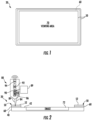
- Figures 1 and 2 illustrate an example display 20, which is not forming part of the claimed invention.
- display 20 provides an encoded pattern beneath the front surface of the border surrounding a viewing area.
- the encoded pattern underlying the border facilitates the detection of the positioning of an electro-optical pen when portions of the electro-optical pen overlie the border.
- Display 20 comprises image layer 40, border 50 and encoded pattern 60.
- Image layer 40 comprises at least one layer of electronic componentry to provide a viewing area 70 in which an image 72 (schematically illustrated) may be presented.
- image layer 40 comprises liquid crystal display electronics and componentry.
- image layer 40 comprises other image producing technology that presents optically visible (visible to the human eye) pictures, graphics, icons or other images in viewing area 70.
- Border 50 comprises a band or frame extending at least partially about viewing area 70.
- Border 50 has a front or upper face 52 facing away from image layer 40.
- face 52 is illustrated as being flat and substantially parallel to the front or top face 42 of image layer 40, in other implementations, face 52 may be rounded, stepped or inclined. In some implementations, face 52 may be beveled or may partially extend about viewing area 70 with gaps or openings within or through border 50.
- Border 50 is formed from a material or materials so as to be visibly opaque and near infrared transparent.
- visibly opaque means that a material cannot transmit light having a wavelength in the range of 400 nm to 700 nm. In the example illustrated, light having a wavelength of at least 400 nm and no greater than 700 nm cannot pass through border 50.
- visibly transparent means that a material can transmit light having a wavelength in the range of 400 nm to 700 nm.
- near infrared transparent means that a material is transparent to, is able to transmit, light of at least one wavelength within the spectrum of wavelengths between 700 nm and 1.4 um.
- a material that transmits any and all wavelengths of light within the range of 700 nm and 1.4 um is “near infrared transparent”.
- a material that transmits a narrow range or a narrow subset of wavelengths of light within (that is smaller than) the broader range of 700 nm and 1.4 um is “near infrared transparent”.
- a material that transmits a wavelength of light of 850 nm, but may not transmit other wavelength of light within the range of 700 nm to 1.4 um is “near infrared transparent”.
- border 50 is transmissive to a smaller range of wavelengths of light contained within the larger range of 700 nm to 1.4 um, wherein the smaller range of wavelength of light is prescribed by the operational specifications of an electro-optical pen to be used with border 50.
- Border 50 is sufficiently "near infrared transparent" such that near infrared pulses of wavelengths of light may be transmitted from an infrared emitter of an input stylus or electro-optical (EO) pen, through border 50 and into impingement with encoded pattern 60 and such that near infrared wavelengths of light reflected off the encoded pattern pass once again through border 50 for being sensed by a camera or other sensor of the input stylus or pen.
- border 50 is black in color to the human eye. In other implementations, border 50 may have other colors.
- border 50 comprises a layer of material that is visibly opaque and near infrared transparent adjacent to and along face 52 of border 50.
- the entire thickness of border 50 comprises a layer visibly opaque near-infrared transparent material.
- border 50 may comprise a stack of layers which includes a layer of visibly opaque near-infrared transparent material.
- any additional layers disposed between the visibly opaque, infrared transparent layer of border 50 and encoded pattern 60 are also near infrared transparent.
- such additional layers disposed between the visible opaque, infrared transparent layer border 50 and encoded pattern 60 may be visibly transparent.
- the visibly opaque near infrared transparent layer of border 50 is sandwiched between encoded pattern 60 and other cover layers.
- the other cover layer or layers that overlie the visibly opaque near infrared transparent layer are also near infrared transparent.
- the other cover layer or layers, while being near infrared transparent may be visibly opaque or may be visibly transparent.
- the visibly opaque near infrared transparent layer of border 50 may comprise a material, such as an ink, commercially available as ADA6212 from H.W. Sands Corporation which has a transmission percentage of less than 10% for wavelengths of electromagnetic radiation up to approximately 680 nm and which drastically increases to a transmission percentage of at least 65% for wavelengths of electromagnetic radiation of 700 nm and to a transmission percentage of at least 85% for wavelengths of electromagnetic radiation of at least 720 nm.
- a material such as an ink, commercially available as ADA6212 from H.W. Sands Corporation which has a transmission percentage of less than 10% for wavelengths of electromagnetic radiation up to approximately 680 nm and which drastically increases to a transmission percentage of at least 65% for wavelengths of electromagnetic radiation of 700 nm and to a transmission percentage of at least 85% for wavelengths of electromagnetic radiation of at least 720 nm.
- the visibly opaque near infrared transparent layer of border 50 may comprise a visibly-opaque IR-transmitting (VOIRT) screen ink commercially available as SPECTRE 110 from Epolin which has a transmission percentage of less than 1% for wavelengths of electromagnetic radiation between 200 and 675 nm and which drastically increases to a transmission percentage of at least 70% for wavelengths of electromagnetic radiation greater than 835 nm.
- VOIRT visibly-opaque IR-transmitting
- the visibly opaque near infrared transparent layer of border 50 may comprise a visibly-opaque IR-transmitting (VOIRT) polycarbonate resin commercially available as MAKROLON 2407-970401 (1 mm), 2407-971000 (1 mm) or AX2477-900346 (1 mm) from Bayer Material Science which have transmission percentages of less than 1% for wavelengths of electromagnetic radiation between 400 and 675 nm and which drastically increases to a transmission percentage of at least 90% for wavelengths of electromagnetic radiation greater than 800 nm, 800 nm and 850 nm, respectively.
- VOIRT visibly-opaque IR-transmitting
- Encoded pattern 60 comprises dots or other markings having a pattern or layout that, when "read” by an electro-optical pen, indicate the positioning of the nib of the electro-optical pen.
- Encoded pattern 60 serves as a coordinate system.
- encoded pattern 60 is provided by a dot film secured beneath face 52 of border 50.
- encoded pattern 60 comprises near infrared reflective dots or markings on a near-infrared absorbing background. Reflective in the context means reflective back at the pen or stylus where the NIR irradiance is coming from and the NIR viewing imager is located. This type of refection is termed backscattered reflection, retro-reflection or diffuse reflection.
- Absorbing in this context can be to actually absorb the NIR irradiance or to reflect it directionally in a manner such that the reflected NIR irradiance is not reflected back at the pen. Specular or mirror-like reflection would do this for most tilt orientations of the pen.
- the pattern (dots) would diffusely reflect the NIR irradiance and the background would absorb via transmission into the chassis of the display as well as absorb via specular reflection of the NIR irradiance away from the pen.
- encoded pattern 60 comprises near-infrared absorbing dots or markings on a near infrared reflective background. The same expanded definitions of reflection and absorption as described above hold for this embodiment as well.
- encoded pattern 60 comprises dots that are positioned relative to one another for a 6 x 6 array that encode the pens absolute position two within plus -150 ⁇ m.
- the encoded pattern of dots provides a resolution of approximately 20 ⁇ m or 1335 lines print.
- the dots of encoded pattern 60 have an average pitch of approximate 300 ⁇ m.
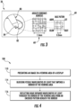
- Figure 3 illustrates one example of encoded pattern 60 as captured and read by an example electro-optical pen 80 having a pointer or nib 82 and a near-infrared transmitting and receiving window 84.
- encoded pattern 60 may comprise other coordinate systems or patterns of dots or markings.
- encoded pattern 60 extends beneath border 50. In one implementation, encoded pattern 60 extends at least 5 mm outwards from the edge of viewing area 70 towards the outer periphery or edge of border 50. In other implementations, encoded pattern 60 may extend a greater distance from the edge of viewing area 70 towards the outer edge of border 50. In some implementations, encoded pattern 60 may extend beneath an entirety of face 52 of border 50. As will be described hereafter, in yet other implementations, encoded pattern 60 may extend beneath viewing area 70 as well. In some implementations, encoded pattern 60 may extend along a band adjacent to and along border 50 within viewing area 70. In yet other implementations, as illustrated hereafter, encoded pattern 60 may cover an entirety of viewing area 70 while extending beyond viewing area 70 beneath border 50.
- Figure 4 is a flow diagram of an example method 100 that may be carried out using a display of the present disclosure. Although method 100 is described as being carried out by display 20, it should be recognized that method 100 may be carried out by any of the displays described in the present disclosure or by other displays having a visibly opaque near-infrared transparent border extending about a viewing area and over and encoded pattern. As indicated by block 110 in Figure 4 , display 20 presents image 72 in a viewing area 70.
- border 50 of viewing area 70 blocks visible wavelengths of light that impinge the border 50.
- near infrared wavelengths of light are reflected through border 50 from encoded pattern 60 beneath border 50.
- the border 50 appears black or some other opaque color to a person using display 20.
- an electro-optical pen is able to "see-through" border 50 and sense the underlying encoded pattern to determine its position and to determine what input is being selected by the person manipulating the pen when the pen is positioned over border 50.
- a text or graphic is "drawn" in the viewing area, simulating writing or drawing on the screen with the pen.
- Figure 2 schematically illustrates the example electro-optical pen 80 which directs near infrared wavelengths of light through border 50 and into impingement with encoded pattern 60, wherein the near infrared wavelengths of light are reflected back through border 50 and are sensed by pen 80.
- pen 80 comprises a near infrared light emitter in the form of a light-emitting diode 86.
- the near-infrared light has a wavelength of approximately 850 nm and LED pulse on duration of approximately 1/10,000 of a second (100 microseconds) at a repetition rate of 30 Hz.
- the near-infrared light may be provided at other near-infrared wavelengths, other durations and other frequencies.
- the near-infrared light 88 passes through face 52 of border 50 and is reflected off of encoded pattern 60.
- the pattern of reflected near infrared light 89 is captured by a sensing device in the form of a camera 90.
- camera 90 comprises a 100 x 100 element CMOS imager. Via an imaging lens (provided at window 84, shown in Figure 3 ), camera 90 views a 14 x 14 array of positionally encoded dots.
- the pen firmware 92 selects and uses an array of 6 x 6 dots to determine the location of the pen tip or nib 82 (shown in Figure 3 ).
- the determined position is transmitted by a transmitter 94 to other remote componentry of display 20 and/or the computing or processing system associated with display 20.
- transmitter 94 comprises a Bluetooth emitter.
- pen 80 may comprise other electronic componentry and may operate in other fashions to capture an image of the encoded pattern 60 of dots and to determine the position of nib 82 using the captured image.
- FIGS 5 and 6 illustrate display 220, a particular implementation of display 20.
- Display 220 is similar to display 20 described above except that 2. according to the claimed invention, the encoded pattern 60 of display 220 is illustrated as continuously extending across the viewing area 70, in addition to extending below a majority of a width of border 50. Encoded pattern 60 is covered or protected by an overlying transparent layer 246 which may comprise an optically or visibly transparent glass or an optically or visibly transparent polymer.
- encoded pattern 60 extends at least from the edge of viewing area 70 outwards away from the center of viewing area 70 by a distance sufficient to underlie a near infrared transmission and capture window of an electro-optical pen when the nib (the point) of the stylus or pen is positioned against (and in contact with) the edge of border 50 at the edge of viewing area 70.
- encoded pattern 60 may extend at least 5 mm beyond the edge of viewing area 70 below border 50.
- encoded pattern 60 may extend beneath the entirety of border 50.
- encoded pattern 60 extends over any images 72 presented by imaging layer 40.
- the size of the individual marks or dots of encoded pattern 60 are sufficiently small so as to not substantially interfere with the viewing of image 72 (other than possibly a slight graying or darkening of the display screen).
- Display 220 facilitates the use of encoded pattern 60 to determine the positioning of pen 80 and the selected input as designated by the positioning of pen 80 when pen 80 is positioned over viewing area 70 and any images 72.
- Display 220 further facilitates the use of encoded pattern 60 to determine the positioning of pen 80 and the selected input as designated by the positioning of pen 80 when pen 80 is positioned over border 50.
- Figure 7 illustrates the use of display 220 when nib 82 of pen 80 is in contact with viewing area 70 proximate to the inner edge 52 of border 50.
- a program may present an image, icon, link, text or other graphical user interface 225 within viewing area 70 along edge 72. Positioning of nib 82 in contact with or over graphical user interface to 25 may correspond to an input to the system employing display 220.
- system 220 associates an area 227 (indicated by broken lines) of dots of the encoded pattern 60 that encloses the graphical user interface 225 of viewing area 70 and that additionally extends beyond edge 52 beneath border 50 with the graphical user interface 225.
- pen 80 may accurately identify the positioning of nib 82 as being in contact with graphical user interface 225 even though pen 80 may be capturing a region 229 of encoded pattern 60 outside of viewing area 70 and outside of the portion of encoded pattern 60 directly underlying the graphical user interface 225 being presented in viewing area 70.
- the positioning of pen 80 is tracked, wherein the images presented by the display include a line corresponding to prior detective positions of nib 82 such that pen 80 "draws” a line across viewing area 70 in response to the nib 82 being slid across viewing area 70.
- the extension of encoded pattern 60 beneath border 50 facilitates such "drawing" by pen 80 closer to the actual physical edge of border 50. As a result, a greater portion of viewing area 70 may be drawn upon by pen 80.
- Figure 8 is a sectional view of a portion of an example display 320, a particular implementation of display 20.
- Display 320 comprises imaging layer 340, dot film 342 providing encoded pattern 60, sensor glass 344, cover glass 346 and visibly opaque near-infrared transparent coating or layer 348 providing border 50.
- Imaging layer 340 is similar to imaging layer 40 described above.
- imaging layer 340 may comprise liquid crystal diode pixels. In other implementations, imaging layer 340 may comprise other imaging technologies.
- Dot film 342 is adhered in front or on top of imaging layer 340 by an intermediate transparent adhesive layer 352.
- Dot film 342 provides encoded pattern 60 described above.
- Sensor glass 344 comprises a visible or optically transparent layer of glass or other visibly transparent material adhered in front of or on top of dot film 342 by adhesive layer 354.
- Sensor glass 344 covers and protects dot film 342 and imaging layer 340.
- Cover glass 346 comprises a layer of glass or other visibly transparent material, such as a transparent polymer, extending across and on top of sensor glass 344. Cover glass 346 is adhered to sensor glass 344 by adhesive layer 356. Cover glass 346 forms the border of the display and supports visibly opaque near-infrared transparent coating or layer 348.
- Layer 348 extends on a face of cover glass 346 between cover glass 346 and sensor glass 344. Layer 348 is coated upon face 360 of cover glass 346 and extends over portions of dot film 342. Interior edges of layer 348 border and define the interior viewing area 70. In other implementations, layer 348 may alternatively be formed on the top outermost face of cover glass 346. In yet other implementations, layer 348 may alternatively be formed on either major face of sensor glass 344. In particular implementations, layer 348 may be formed from any of the VOIRT materials described above with respect to border 50.
- FIGS 9 and 10 illustrate display 420, another example implementation of display 20.
- Display 420 is similar to display 220 except that display 420 additionally comprises touch sensor 480 and graphic input interfaces 482A, 482B, 482C, 482D and 482E (collectively referred to as graphic input interfaces 482). Those remaining elements of display 420 which correspond to elements of display 20 or display 220 are numbered similarly.
- Touch sensor 480 comprises a touch sensitive interface panel which outputs electrical signals in response to being touched, such as being touched by a person's finger or in response to being touched or contacted by the tip, point or nib of an input stylus or electro-optical pen, such as nib 82 of pen 80 described above.
- touch sensor 480 extends within viewing area 70 while underlying a dot film 342 forming encoded pattern 60.
- touch sensor 480 overlies image layer 40. In other implementations, touch sensor 480 may be omitted.
- Graphic input interfaces 482 comprise graphics that are printed, laminated, coated or otherwise provided on border 50, overlying portions of encoded pattern 60 that extend beneath border 50.
- interfaces 42 are formed on top of surface 52 of border 50.
- interfaces 42 may be covered by at least one visibly or optically transparent layer, wherein the layer is also near-infrared transparent.
- each of graphic input interfaces 482 comprises an outline of an icon or other graphic, wherein the nib 42 of the electro-optical pen, such as pen 80, may be positioned within the outline to provide input.
- each of interfaces 482 comprises a solid visibly opaque graphic that is also near infrared transparent.
- each of interfaces 482 may comprise a visibly opaque near-infrared transparent ink printed or otherwise coated upon border 50.
- the visibly opaque near-infrared transparent ink form each of interfaces 482 has colors different than that of border 50.
- Each of graphic input interfaces 482 are provided at predefined distinct locations or over predefined distinct sets of dots of encoded pattern 60 below border 50.
- the electro-optical pen may output signals triggering execution of a particular command or selection corresponding to the overlying interface 482.
- the pen 80 may output signals which trigger and operation corresponding to interface 482D (in the example illustrated, a print command).
- unique sets/patterns of dots may be reserved for communication of underlying commands or selections universally and response to such detection or determination triggers execution of said commands or selections while concurrently providing local positon orientation as well.
- graphic input interface 42 facilitates the input of commands using pen 80 and the underlying portions of encoded pattern 60 along border 50.
- border 50 provides an additional area that serves as an input interface, preserving the available area of viewing area 70 for the presentation of more dynamic, changing or program specific graphical user interfaces 490, 492 in viewing area 70.
- Such graphic user interfaces 490, 492 may be selected using the interaction of the pen 80 with those portions of encoded pattern 60 underlying the graphical user interfaces 490, 492 or using touch sensor 480.
- display 420 facilitates the constant presentation of the more application universal or static interfaces 482 (interfaces for commands or selections that do not change or lose relevance in spite of different applications or programs being executed and presented in the viewing area 70) while preserving viewing area 70 for being drawn upon by pen 80.
- the movement of pen 80 across viewing area 70 is tracked, wherein such tracking is displayed in viewing area 70 and results in a pen drawn graphic or text 494 (schematically illustrated).
- display 420 may be provided with additional, fewer or alternative commands or selections along border 50.
- interface 42 may be provided along a single side of border 50 or may be provided continuously about border 50.
- interface 482 may be omitted.
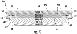
- Figure 11 is a sectional view illustrating display 520, another example implementation of display 20.
- Display 720 is similar to display 420 except that the encoded pattern 60 is provided by a dot film that underlies the touch sensor of display 520.
- Those components or elements of display 520 which correspond to components or elements of any of the above-described displays are numbered similarly.
- Display 520 comprises image layer 40, dot film 342 providing encoded pattern 60, sensor glass 538, touch sensor 540, cover glass 546 and visibly opaque near-infrared transparent mask or layer 548.
- dot film 342 providing encoded pattern 60 is laminated between sensor glass 538 and image layer 40.
- Sensor glass 344 covers and protects touch sensor 540.
- touch sensor 540 is secured on top of sensor glass 344 with touch sensor 540 sandwiched between sensor glass 538 and cover glass 546.
- touch sensor 540 comprises an indium tin oxide touch sensor films 542, 544 for sensing in X and Y coordinates, respectively.
- touch sensor 540 may comprise other touch sensitive sensing technologies.
- Cover glass 546 comprises a layer of glass or other transparent material, such as a transparent polymer, extending across and on top of touch sensor 540. Cover glass 546 forms the border of the display and supports visibly opaque near-infrared transparent coating or layer 548.
- Layer 548 extends on a face of cover glass 546 between cover glass 546 and dot film 542. Layer 548 is coated upon face 560 of cover glass 546 and extends over portions of dot film 538. Interior edges of layer 548 border and define the interior viewing area 70. In other implementations, layer 548 may alternatively be formed on the top outermost face of cover glass 546. In particular implementations, layer 548 may be formed from any of the VOIRT materials described above.
Description
- Many electronic devices include displays having viewing areas in which information is visibly presented. Such viewing areas may include an underlying encoded pattern which reflects pulses of near infrared light to indicate a position of an electro-optical pen.
-
WO 2015/141105 A1 discloses an optical film having a display part and a bezel part formed around the display part, wherein: a pattern that expresses position information is provided on the back surface of the display part; a pattern that expresses position information is provided on the back surface of the bezel part; and the optical film is provided with a first bezel decorative layer that absorbs specific visible light out of incident light and allows infrared light to pass through and a second bezel decorative layer that reflects infrared light out of the light that has passed through the first bezel decorative layer. -
US 2006/238517 discloses an electronic device having a display and a touch sensitive bezel surrounding the display. Areas on the bezel are designated for controls used to operate the electronic device.WO 2016/010534 discloses a display including a display stack to generate a digital display image. A media layer includes a plurality of diffusive emissive elements disposed in a predetermined pattern. The diffusive emissive elements on the media layer emit a scattered signal in response to light incident to the media layer.US 2014/168089 discloses systems and methods for calibrating a photoluminescent indicia-based digitizer system with a display, the photoluminescent indicia uniquely identifying local areas of a substrate. -
-
Figure 1 is a front view of an example display. -
Figure 2 is a sectional view of the example display ofFigure 1 illustrating the example display interacting with an example electro-optical pen. -
Figure 3 is an enlarged plan view of a portion of the display ofFigure 1 , illustrating an encoded pattern that interacts with the electro-optical pen. -
Figure 4 is a flow diagram of an example method for use of the example display. -
Figure 5 is a front view of another example display. -
Figure 6 is a sectional view of the example display ofFigure 5 illustrating the example display interacting with example electro-optical pens. -
Figure 7 is an enlarged fragmentary view of the display ofFigure 5 illustrating interaction of an electro-optical pen along a border of the display. -
Figure 8 is a sectional view of another example display. -
Figure 9 is a sectional view of another example display. -
Figure 10 is a front view of the example display ofFigure 9 . -
Figure 11 is a sectional view of another example display. - The viewing area of most displays is surrounded by a frame or border. In many displays, the border is visibly opaque to conceal underlying electrical traces, connections or componentry. The underlying encoded pattern in the viewing area of a display terminates inwardly spaced from or at the perimeter of the viewing area. In other words, the underlying encoded pattern does not extend beneath the border.
- Electro-optical pens may include a nib that contacts the viewing area of the display. Such pens often include a window through which pulses of near infrared light are directed towards the underlying encoded pattern and through which reflections from the underlying encoded pattern are received by a sensor to detect the positioning of the nib. Because the window is often offset from the nib, the sensor may be unable to interact with the encoded pattern that underlies the nib when the nib is positioned against the viewing area along the edge of the border. As a result, input using the electro-optical pen adjacent the edge of the border is limited or not available.
- Many displays may be relatively small in size. As a result, the available surface area of the viewing area for providing icons by which commands, selections or other input may be made using the electro-optical pen is limited. Providing such icons for input using the electro-optical pen produces available space of the viewing area for presenting other information or other images.
- The present disclosure provides a display that provides an encoded pattern beneath the surface of the border. While remaining visibly opaque so as to continue to conceal underlying electronics, the border is near infrared transparent. As a result, the sensor of the electro-optical pen is able to sense near infrared light reflected off of the encoded pattern beneath the surface of the border and is able to detect the positioning of the electro-optical pen when the nib is along the edge of the border within the viewing area or is positioned on top of and in contact with the upper surface of the border. The display of the present disclosure offers a greater usable area for input of selections or commands using an electro-optical pen.
-
Figures 1 and 2 illustrate anexample display 20, which is not forming part of the claimed invention. As will be described hereafter,display 20 provides an encoded pattern beneath the front surface of the border surrounding a viewing area. The encoded pattern underlying the border facilitates the detection of the positioning of an electro-optical pen when portions of the electro-optical pen overlie the border.Display 20 comprisesimage layer 40,border 50 and encodedpattern 60. -
Image layer 40 comprises at least one layer of electronic componentry to provide aviewing area 70 in which an image 72 (schematically illustrated) may be presented. In one implementation,image layer 40 comprises liquid crystal display electronics and componentry. In other implementations,image layer 40 comprises other image producing technology that presents optically visible (visible to the human eye) pictures, graphics, icons or other images inviewing area 70. -
Border 50 comprises a band or frame extending at least partially aboutviewing area 70. Border 50 has a front orupper face 52 facing away fromimage layer 40. Althoughface 52 is illustrated as being flat and substantially parallel to the front ortop face 42 ofimage layer 40, in other implementations,face 52 may be rounded, stepped or inclined. In some implementations,face 52 may be beveled or may partially extend aboutviewing area 70 with gaps or openings within or throughborder 50. -
Border 50 is formed from a material or materials so as to be visibly opaque and near infrared transparent. The term "visibly opaque" means that a material cannot transmit light having a wavelength in the range of 400 nm to 700 nm. In the example illustrated, light having a wavelength of at least 400 nm and no greater than 700 nm cannot pass throughborder 50. The term "visibly transparent" means that a material can transmit light having a wavelength in the range of 400 nm to 700 nm. The term "near infrared transparent" means that a material is transparent to, is able to transmit, light of at least one wavelength within the spectrum of wavelengths between 700 nm and 1.4 um. For example, a material that transmits any and all wavelengths of light within the range of 700 nm and 1.4 um is "near infrared transparent". Likewise, a material that transmits a narrow range or a narrow subset of wavelengths of light within (that is smaller than) the broader range of 700 nm and 1.4 um is "near infrared transparent". For example, a material that transmits a wavelength of light of 850 nm, but may not transmit other wavelength of light within the range of 700 nm to 1.4 um is "near infrared transparent". In some implementations,border 50 is transmissive to a smaller range of wavelengths of light contained within the larger range of 700 nm to 1.4 um, wherein the smaller range of wavelength of light is prescribed by the operational specifications of an electro-optical pen to be used withborder 50.Border 50 is sufficiently "near infrared transparent" such that near infrared pulses of wavelengths of light may be transmitted from an infrared emitter of an input stylus or electro-optical (EO) pen, throughborder 50 and into impingement with encodedpattern 60 and such that near infrared wavelengths of light reflected off the encoded pattern pass once again throughborder 50 for being sensed by a camera or other sensor of the input stylus or pen. In one implementation,border 50 is black in color to the human eye. In other implementations,border 50 may have other colors. - In one implementation,
border 50 comprises a layer of material that is visibly opaque and near infrared transparent adjacent to and alongface 52 ofborder 50. In one implementation, the entire thickness ofborder 50 comprises a layer visibly opaque near-infrared transparent material. In other implementations,border 50 may comprise a stack of layers which includes a layer of visibly opaque near-infrared transparent material. In such an implementation, any additional layers disposed between the visibly opaque, infrared transparent layer ofborder 50 and encodedpattern 60 are also near infrared transparent. In such implementations, such additional layers disposed between the visible opaque, infraredtransparent layer border 50 and encodedpattern 60 may be visibly transparent. - In yet other implementations, the visibly opaque near infrared transparent layer of
border 50 is sandwiched between encodedpattern 60 and other cover layers. In such an implementation, the other cover layer or layers that overlie the visibly opaque near infrared transparent layer are also near infrared transparent. In such an implementation, the other cover layer or layers, while being near infrared transparent, may be visibly opaque or may be visibly transparent. - In one implementation, the visibly opaque near infrared transparent layer of
border 50 may comprise a material, such as an ink, commercially available as ADA6212 from H.W. Sands Corporation which has a transmission percentage of less than 10% for wavelengths of electromagnetic radiation up to approximately 680 nm and which drastically increases to a transmission percentage of at least 65% for wavelengths of electromagnetic radiation of 700 nm and to a transmission percentage of at least 85% for wavelengths of electromagnetic radiation of at least 720 nm. In yet another implementation, the visibly opaque near infrared transparent layer ofborder 50 may comprise a visibly-opaque IR-transmitting (VOIRT) screen ink commercially available asSPECTRE 110 from Epolin which has a transmission percentage of less than 1% for wavelengths of electromagnetic radiation between 200 and 675 nm and which drastically increases to a transmission percentage of at least 70% for wavelengths of electromagnetic radiation greater than 835 nm. In yet another implementation, the visibly opaque near infrared transparent layer ofborder 50 may comprise a visibly-opaque IR-transmitting (VOIRT) polycarbonate resin commercially available as MAKROLON 2407-970401 (1 mm), 2407-971000 (1 mm) or AX2477-900346 (1 mm) from Bayer Material Science which have transmission percentages of less than 1% for wavelengths of electromagnetic radiation between 400 and 675 nm and which drastically increases to a transmission percentage of at least 90% for wavelengths of electromagnetic radiation greater than 800 nm, 800 nm and 850 nm, respectively. In yet other implementations, other VOIRT materials may be utilized. - Encoded
pattern 60 comprises dots or other markings having a pattern or layout that, when "read" by an electro-optical pen, indicate the positioning of the nib of the electro-optical pen. Encodedpattern 60 serves as a coordinate system. In one implementation, encodedpattern 60 is provided by a dot film secured beneathface 52 ofborder 50. In one implementation, encodedpattern 60 comprises near infrared reflective dots or markings on a near-infrared absorbing background. Reflective in the context means reflective back at the pen or stylus where the NIR irradiance is coming from and the NIR viewing imager is located. This type of refection is termed backscattered reflection, retro-reflection or diffuse reflection. Absorbing in this context can be to actually absorb the NIR irradiance or to reflect it directionally in a manner such that the reflected NIR irradiance is not reflected back at the pen. Specular or mirror-like reflection would do this for most tilt orientations of the pen. For example in one embodiment the pattern (dots) would diffusely reflect the NIR irradiance and the background would absorb via transmission into the chassis of the display as well as absorb via specular reflection of the NIR irradiance away from the pen. In yet other implementations, encodedpattern 60 comprises near-infrared absorbing dots or markings on a near infrared reflective background. The same expanded definitions of reflection and absorption as described above hold for this embodiment as well. - In one implementation, encoded
pattern 60 comprises dots that are positioned relative to one another for a 6 x 6 array that encode the pens absolute position two within plus -150 µm. The encoded pattern of dots provides a resolution of approximately 20 µm or 1335 lines print. In one implementation, the dots of encodedpattern 60 have an average pitch of approximate 300 µm.Figure 3 illustrates one example of encodedpattern 60 as captured and read by an example electro-optical pen 80 having a pointer ornib 82 and a near-infrared transmitting and receivingwindow 84. In other implementations, encodedpattern 60 may comprise other coordinate systems or patterns of dots or markings. - In the example illustrated, encoded
pattern 60 extends beneathborder 50. In one implementation, encodedpattern 60 extends at least 5 mm outwards from the edge ofviewing area 70 towards the outer periphery or edge ofborder 50. In other implementations, encodedpattern 60 may extend a greater distance from the edge ofviewing area 70 towards the outer edge ofborder 50. In some implementations, encodedpattern 60 may extend beneath an entirety offace 52 ofborder 50. As will be described hereafter, in yet other implementations, encodedpattern 60 may extend beneathviewing area 70 as well. In some implementations, encodedpattern 60 may extend along a band adjacent to and alongborder 50 withinviewing area 70. In yet other implementations, as illustrated hereafter, encodedpattern 60 may cover an entirety ofviewing area 70 while extending beyondviewing area 70 beneathborder 50. -
Figure 4 is a flow diagram of anexample method 100 that may be carried out using a display of the present disclosure. Althoughmethod 100 is described as being carried out bydisplay 20, it should be recognized thatmethod 100 may be carried out by any of the displays described in the present disclosure or by other displays having a visibly opaque near-infrared transparent border extending about a viewing area and over and encoded pattern. As indicated byblock 110 inFigure 4 ,display 20presents image 72 in aviewing area 70. - As indicated by
block 114 inFigure 4 ,border 50 ofviewing area 70 blocks visible wavelengths of light that impinge theborder 50. At the same time, as indicated byblock 116, near infrared wavelengths of light are reflected throughborder 50 from encodedpattern 60 beneathborder 50. As a result, theborder 50 appears black or some other opaque color to aperson using display 20. At the same time, an electro-optical pen is able to "see-through"border 50 and sense the underlying encoded pattern to determine its position and to determine what input is being selected by the person manipulating the pen when the pen is positioned overborder 50. In some implementations, aspen 80 is moved across the viewing area (with the position of the pen being detected as it is being moved), a text or graphic is "drawn" in the viewing area, simulating writing or drawing on the screen with the pen. -
Figure 2 schematically illustrates the example electro-optical pen 80 which directs near infrared wavelengths of light throughborder 50 and into impingement with encodedpattern 60, wherein the near infrared wavelengths of light are reflected back throughborder 50 and are sensed bypen 80. As shown byFigure 2 ,pen 80 comprises a near infrared light emitter in the form of a light-emittingdiode 86. - In one implementation, the near-infrared light has a wavelength of approximately 850 nm and LED pulse on duration of approximately 1/10,000 of a second (100 microseconds) at a repetition rate of 30 Hz. In other implementations, the near-infrared light may be provided at other near-infrared wavelengths, other durations and other frequencies. The near-infrared light 88 passes through
face 52 ofborder 50 and is reflected off of encodedpattern 60. - The pattern of reflected near
infrared light 89 is captured by a sensing device in the form of acamera 90. In one implementation,camera 90 comprises a 100 x 100 element CMOS imager. Via an imaging lens (provided atwindow 84, shown inFigure 3 ),camera 90 views a 14 x 14 array of positionally encoded dots. From a larger set, thepen firmware 92 selects and uses an array of 6 x 6 dots to determine the location of the pen tip or nib 82 (shown inFigure 3 ). In the example illustrated, the determined position is transmitted by atransmitter 94 to other remote componentry ofdisplay 20 and/or the computing or processing system associated withdisplay 20. In one implementation,transmitter 94 comprises a Bluetooth emitter. In other implementations,pen 80 may comprise other electronic componentry and may operate in other fashions to capture an image of the encodedpattern 60 of dots and to determine the position ofnib 82 using the captured image. -
Figures 5 and 6 illustratedisplay 220, a particular implementation ofdisplay 20.Display 220 is similar to display 20 described above except that 2. according to the claimed invention, the encodedpattern 60 ofdisplay 220 is illustrated as continuously extending across theviewing area 70, in addition to extending below a majority of a width ofborder 50. Encodedpattern 60 is covered or protected by an overlyingtransparent layer 246 which may comprise an optically or visibly transparent glass or an optically or visibly transparent polymer. - In one implementation, encoded
pattern 60 extends at least from the edge ofviewing area 70 outwards away from the center ofviewing area 70 by a distance sufficient to underlie a near infrared transmission and capture window of an electro-optical pen when the nib (the point) of the stylus or pen is positioned against (and in contact with) the edge ofborder 50 at the edge ofviewing area 70. In one implementation, encodedpattern 60 may extend at least 5 mm beyond the edge ofviewing area 70 belowborder 50. In one implementation, encodedpattern 60 may extend beneath the entirety ofborder 50. Those remaining components ofdisplay 220 which correspond to components ofdisplay 20 are numbered similarly or are shown inFigures 1-3 . - As shown by
Figure 6 , encodedpattern 60 extends over anyimages 72 presented byimaging layer 40. The size of the individual marks or dots of encodedpattern 60 are sufficiently small so as to not substantially interfere with the viewing of image 72 (other than possibly a slight graying or darkening of the display screen).Display 220 facilitates the use of encodedpattern 60 to determine the positioning ofpen 80 and the selected input as designated by the positioning ofpen 80 whenpen 80 is positioned overviewing area 70 and anyimages 72.Display 220 further facilitates the use of encodedpattern 60 to determine the positioning ofpen 80 and the selected input as designated by the positioning ofpen 80 whenpen 80 is positioned overborder 50. -
Figure 7 illustrates the use ofdisplay 220 whennib 82 ofpen 80 is in contact withviewing area 70 proximate to theinner edge 52 ofborder 50. In some implementations, a program may present an image, icon, link, text or othergraphical user interface 225 withinviewing area 70 alongedge 72. Positioning ofnib 82 in contact with or over graphical user interface to 25 may correspond to an input to thesystem employing display 220. To accommodate the positioning ofnib 82 adjacent to edge 52 over thegraphical user interface 225,system 220 associates an area 227 (indicated by broken lines) of dots of the encodedpattern 60 that encloses thegraphical user interface 225 ofviewing area 70 and that additionally extends beyondedge 52 beneathborder 50 with thegraphical user interface 225. As a result,pen 80 may accurately identify the positioning ofnib 82 as being in contact withgraphical user interface 225 even thoughpen 80 may be capturing aregion 229 of encodedpattern 60 outside ofviewing area 70 and outside of the portion of encodedpattern 60 directly underlying thegraphical user interface 225 being presented inviewing area 70. - In some implementations, the positioning of
pen 80 is tracked, wherein the images presented by the display include a line corresponding to prior detective positions ofnib 82 such thatpen 80 "draws" a line acrossviewing area 70 in response to thenib 82 being slid acrossviewing area 70. In such circumstances, the extension of encodedpattern 60 beneathborder 50 facilitates such "drawing" bypen 80 closer to the actual physical edge ofborder 50. As a result, a greater portion ofviewing area 70 may be drawn upon bypen 80. -
Figure 8 is a sectional view of a portion of anexample display 320, a particular implementation ofdisplay 20.Display 320 comprisesimaging layer 340,dot film 342 providing encodedpattern 60,sensor glass 344,cover glass 346 and visibly opaque near-infrared transparent coating orlayer 348 providingborder 50.Imaging layer 340 is similar toimaging layer 40 described above. In one implementation,imaging layer 340 may comprise liquid crystal diode pixels. In other implementations,imaging layer 340 may comprise other imaging technologies. -
Dot film 342 is adhered in front or on top ofimaging layer 340 by an intermediate transparentadhesive layer 352.Dot film 342 provides encodedpattern 60 described above.Sensor glass 344 comprises a visible or optically transparent layer of glass or other visibly transparent material adhered in front of or on top ofdot film 342 byadhesive layer 354.Sensor glass 344 covers and protectsdot film 342 andimaging layer 340.Cover glass 346 comprises a layer of glass or other visibly transparent material, such as a transparent polymer, extending across and on top ofsensor glass 344.Cover glass 346 is adhered tosensor glass 344 byadhesive layer 356.Cover glass 346 forms the border of the display and supports visibly opaque near-infrared transparent coating orlayer 348. -
Layer 348 extends on a face ofcover glass 346 betweencover glass 346 andsensor glass 344.Layer 348 is coated uponface 360 ofcover glass 346 and extends over portions ofdot film 342. Interior edges oflayer 348 border and define theinterior viewing area 70. In other implementations,layer 348 may alternatively be formed on the top outermost face ofcover glass 346. In yet other implementations,layer 348 may alternatively be formed on either major face ofsensor glass 344. In particular implementations,layer 348 may be formed from any of the VOIRT materials described above with respect toborder 50. -
Figures 9 and 10 illustratedisplay 420, another example implementation ofdisplay 20.Display 420 is similar to display 220 except thatdisplay 420 additionally comprisestouch sensor 480 andgraphic input interfaces display 420 which correspond to elements ofdisplay 20 ordisplay 220 are numbered similarly. -
Touch sensor 480 comprises a touch sensitive interface panel which outputs electrical signals in response to being touched, such as being touched by a person's finger or in response to being touched or contacted by the tip, point or nib of an input stylus or electro-optical pen, such asnib 82 ofpen 80 described above. In the example illustrated,touch sensor 480 extends withinviewing area 70 while underlying adot film 342 forming encodedpattern 60. In the example illustrated,touch sensor 480 overliesimage layer 40. In other implementations,touch sensor 480 may be omitted. - Graphic input interfaces 482 comprise graphics that are printed, laminated, coated or otherwise provided on
border 50, overlying portions of encodedpattern 60 that extend beneathborder 50. In one implementation, interfaces 42 are formed on top ofsurface 52 ofborder 50. In other implementations, interfaces 42 may be covered by at least one visibly or optically transparent layer, wherein the layer is also near-infrared transparent. - In one implementation, each of graphic input interfaces 482 comprises an outline of an icon or other graphic, wherein the
nib 42 of the electro-optical pen, such aspen 80, may be positioned within the outline to provide input. In another implementation, each of interfaces 482 comprises a solid visibly opaque graphic that is also near infrared transparent. For example, in one implementation, each of interfaces 482 may comprise a visibly opaque near-infrared transparent ink printed or otherwise coated uponborder 50. In one implementation, the visibly opaque near-infrared transparent ink form each of interfaces 482 has colors different than that ofborder 50. - Each of graphic input interfaces 482 are provided at predefined distinct locations or over predefined distinct sets of dots of encoded
pattern 60 belowborder 50. In response to a detection or determination that thenib 82 of an electro-optical pen is located over a set of dots of encodedpattern 60, the electro-optical pen may output signals triggering execution of a particular command or selection corresponding to the overlying interface 482. For example, in response to pen 80 transmitting near-infrared light throughinterface 482D, wherein the pulses of near-infrared light are reflected and captured bypen 82 indicatenib 42 is overinterface 482D, thepen 80 may output signals which trigger and operation corresponding to interface 482D (in the example illustrated, a print command). Alternatively, unique sets/patterns of dots may be reserved for communication of underlying commands or selections universally and response to such detection or determination triggers execution of said commands or selections while concurrently providing local positon orientation as well. - The provision of
graphic input interface 42 facilitates the input ofcommands using pen 80 and the underlying portions of encodedpattern 60 alongborder 50. As a result,border 50 provides an additional area that serves as an input interface, preserving the available area ofviewing area 70 for the presentation of more dynamic, changing or program specificgraphical user interfaces viewing area 70. Suchgraphic user interfaces pen 80 with those portions of encodedpattern 60 underlying thegraphical user interfaces touch sensor 480. As further shown byFigure 10 ,display 420 facilitates the constant presentation of the more application universal or static interfaces 482 (interfaces for commands or selections that do not change or lose relevance in spite of different applications or programs being executed and presented in the viewing area 70) while preservingviewing area 70 for being drawn upon bypen 80. In the example illustrated, the movement ofpen 80 across viewing area 70 (based upon the determined positioning ofnib 82 ofpen 80 using encoded pattern 60) is tracked, wherein such tracking is displayed inviewing area 70 and results in a pen drawn graphic or text 494 (schematically illustrated). - Although
graphical user interfaces display 420 may be provided with additional, fewer or alternative commands or selections alongborder 50. In some implementations,interface 42 may be provided along a single side ofborder 50 or may be provided continuously aboutborder 50. In yet other implementations, interface 482 may be omitted. -
Figure 11 is a sectionalview illustrating display 520, another example implementation ofdisplay 20. Display 720 is similar to display 420 except that the encodedpattern 60 is provided by a dot film that underlies the touch sensor ofdisplay 520. Those components or elements ofdisplay 520 which correspond to components or elements of any of the above-described displays are numbered similarly. -
Display 520 comprisesimage layer 40,dot film 342 providing encodedpattern 60,sensor glass 538,touch sensor 540,cover glass 546 and visibly opaque near-infrared transparent mask orlayer 548. As shown byFigure 11 ,dot film 342 providing encodedpattern 60 is laminated betweensensor glass 538 andimage layer 40.Sensor glass 344 covers and protectstouch sensor 540. In the example illustrated,touch sensor 540 is secured on top ofsensor glass 344 withtouch sensor 540 sandwiched betweensensor glass 538 andcover glass 546. In one implementation,touch sensor 540 comprises an indium tin oxidetouch sensor films touch sensor 540 may comprise other touch sensitive sensing technologies. -
Cover glass 546 comprises a layer of glass or other transparent material, such as a transparent polymer, extending across and on top oftouch sensor 540.Cover glass 546 forms the border of the display and supports visibly opaque near-infrared transparent coating orlayer 548. -
Layer 548 extends on a face ofcover glass 546 betweencover glass 546 anddot film 542.Layer 548 is coated uponface 560 ofcover glass 546 and extends over portions ofdot film 538. Interior edges oflayer 548 border and define theinterior viewing area 70. In other implementations,layer 548 may alternatively be formed on the top outermost face ofcover glass 546. In particular implementations,layer 548 may be formed from any of the VOIRT materials described above. - Although the present disclosure has been described with reference to example implementations, workers skilled in the art will recognize that changes may be made in form and detail without departing from the scope of the claimed subject matter. For example, although different example implementations may have been described as including one or more features providing one or more benefits, it is contemplated that the described features may be interchanged with one another or alternatively be combined with one another in the described example implementations or in other alternative implementations. For example, unless specifically otherwise noted, the claims reciting a single particular element also encompass a plurality of such particular elements. The terms "first", "second", "third" and so on in the claims merely distinguish different elements and, unless otherwise stated, are not to be specifically associated with a particular order or particular numbering of elements in the disclosure.
Claims (12)
- A display (220, 320, 530) comprising:an image layer (40, 340) providing a viewing area (70);an encoded pattern (60) overlying the image layer (40), wherein the encoded pattern is embedded in a dot film (342) and the dot film is adhered to the image layer, wherein the encoded pattern contains positional information readable by an infrared receiver (90) of an electro-optical pen (80) to indicate a position of the electro-optical pen (80);a sensor glass (344, 538) adhered to the dot film, on an opposite face of the dot film to the image layer; anda border (50) about the viewing area and overlying the sensor glass, the border being visibly opaque, and being near infrared transparent to light having a wavelength of between 700nm and 1.4um wherein the border is adhered to the sensor glass on an opposite face of the sensor glass to the dot film;wherein the encoded pattern (60) continuously extends from within the viewing area (70) to beneath the border (50).
- The display (220, 320, 520) of claim 1, wherein the encoded pattern (60) extends at least 5 mm beyond the viewing area (70) beneath the border (50).
- The display (220, 320, 520) of claim 1, the display further comprising a touch sensor (218) in the viewing area (70).
- The display (220, 320, 520) of claim 1, wherein the border (50) comprises: a visibly transparent layer; and a visibly opaque, near infrared transparent layer between the visibly transparent layer and the encoded pattern (60) beneath the border.
- The display (220, 320, 520) of claim 1, wherein the border (50) comprises: a visibly transparent layer; and a visibly opaque, near infrared transparent layer between the visibly transparent layer and the encoded pattern (60) beneath the border.
- The display (220, 320, 520) of claim 1, further comprising a graphic on the border (50) over the encoded pattern (60) underlying the border.
- The display (220, 320, 520) of claim 6, wherein the graphic comprises a visibly opaque, near infrared transparent layer.
- The display (220, 320, 520) of claim 6, wherein the graphic indicates an input selection corresponding to the encoded pattern (60) underlying the border (50) proximate the graphic.
- The display (220, 320, 520) of claim 1, wherein the encoded pattern (60) comprises near infrared reflective dots over a near infrared absorptive background.
- The display (220, 320, 520) of claim 1, wherein the encoded pattern (60) comprises near infrared absorptive dots over a near infrared reflective background.
- A method for controlling a system comprising a display (220, 320, 520) and an electro-optical pen (80),the display comprising: an image layer (40, 340) providing a viewing area (70); an encoded pattern (60) overlying the image layer (40), wherein the encoded pattern is embedded in a dot film (342) and the dot film is adhered to the image layer, and wherein the encoded pattern contains positional information readable by an infrared receiver (90) of the electro-optical pen (80) to indicate a position of the electro-optical pen (80);a sensor glass (344, 538) adhered to the dot film, on an opposite face of the dot film to the image layer; and a border (50) about the viewing area and overlying the sensor glass, the border being visibly opaque, and being near infrared transparent to light having a wavelength of between 700nm and 1.4um wherein the border is adhered to the sensor glass on an opposite face of the sensor glass to the dot film;wherein the encoded pattern (60) continuously extends from within the viewing area (70) to beneath the border (50);the method comprising:presenting an image (72) in the viewing area (70) of the display (220, 320, 520);blocking, by the visibly opaque border (50), visible wavelengths of light that impinge the border (50) of the viewing area of the display; andreflecting near infrared wavelengths of light through the near infrared transparent border of the viewing area from the encoded pattern (60) beneath the border.
- The method of claim 11, comprising:emitting the near infrared wavelengths of light by a near infrared light emitter (86) comprised by the electro-optical pen (80) directed toward the encoded pattern (60) underlying the border (50), andreflecting the near infrared wavelengths of light from the encoded pattern through the border area of the viewing area (70) to the receiver (90) of the electro-optical pen (80).
Applications Claiming Priority (1)
| Application Number | Priority Date | Filing Date | Title |
|---|---|---|---|
| PCT/US2016/043195 WO2018017083A1 (en) | 2016-07-20 | 2016-07-20 | Near infrared transparent display border with underlyng encoded pattern. |
Publications (3)
| Publication Number | Publication Date |
|---|---|
| EP3437085A1 EP3437085A1 (en) | 2019-02-06 |
| EP3437085A4 EP3437085A4 (en) | 2019-11-20 |
| EP3437085B1 true EP3437085B1 (en) | 2023-03-08 |
Family
ID=60992396
Family Applications (1)
| Application Number | Title | Priority Date | Filing Date |
|---|---|---|---|
| EP16909676.5A Active EP3437085B1 (en) | 2016-07-20 | 2016-07-20 | Near infrared transparent display border with underlyng encoded pattern. |
Country Status (4)
| Country | Link |
|---|---|
| US (1) | US10620716B2 (en) |
| EP (1) | EP3437085B1 (en) |
| CN (1) | CN109313866B (en) |
| WO (1) | WO2018017083A1 (en) |
Families Citing this family (3)
| Publication number | Priority date | Publication date | Assignee | Title |
|---|---|---|---|---|
| US11182038B2 (en) * | 2020-04-08 | 2021-11-23 | Sigmasense, Llc. | Encoded data pattern touchscreen sensing system |
| DE102020112221A1 (en) | 2020-05-06 | 2021-11-11 | Bayerische Motoren Werke Aktiengesellschaft | Device for a motor vehicle and motor vehicle |
| US11175700B1 (en) | 2020-05-14 | 2021-11-16 | Apple Inc. | Electronic devices with adjustable-appearance housing structures |
Citations (1)
| Publication number | Priority date | Publication date | Assignee | Title |
|---|---|---|---|---|
| US20140168089A1 (en) * | 2012-12-13 | 2014-06-19 | 3M Innovative Properties Company | System and methods for calibrating a digitizer system |
Family Cites Families (34)
| Publication number | Priority date | Publication date | Assignee | Title |
|---|---|---|---|---|
| US5398133A (en) | 1993-10-27 | 1995-03-14 | Industrial Technology Research Institute | High endurance near-infrared optical window |
| US6686910B2 (en) * | 1996-04-22 | 2004-02-03 | O'donnell, Jr. Francis E. | Combined writing instrument and digital documentor apparatus and method of use |
| US9213443B2 (en) | 2009-02-15 | 2015-12-15 | Neonode Inc. | Optical touch screen systems using reflected light |
| US7656393B2 (en) * | 2005-03-04 | 2010-02-02 | Apple Inc. | Electronic device having display and surrounding touch sensitive bezel for user interface and control |
| US8587562B2 (en) | 2002-11-04 | 2013-11-19 | Neonode Inc. | Light-based touch screen using elliptical and parabolic reflectors |
| CN101609383B (en) * | 2006-03-03 | 2014-08-06 | 苹果公司 | Electronic device having display and surrounding touch sensitive bezel for user interface and control |
| JP2008021168A (en) * | 2006-07-13 | 2008-01-31 | Fuji Xerox Co Ltd | Handwriting detection sheet and handwriting system |
| US20090278794A1 (en) * | 2008-05-09 | 2009-11-12 | Smart Technologies Ulc | Interactive Input System With Controlled Lighting |
| CN101833400B (en) * | 2009-03-10 | 2012-06-13 | 广达电脑股份有限公司 | Optical sensing screen and panel sensing method |
| US8731618B2 (en) * | 2009-04-23 | 2014-05-20 | Apple Inc. | Portable electronic device |
| CN101907951B (en) | 2009-06-05 | 2013-04-10 | 鸿富锦精密工业(深圳)有限公司 | Touch control system |
| CN102648444A (en) * | 2009-10-12 | 2012-08-22 | 惠普发展公司,有限责任合伙企业 | Display with an optical sensor |
| US8730184B2 (en) * | 2009-12-16 | 2014-05-20 | 3M Innovative Properties Company | Touch sensitive device with multilayer electrode having improved optical and electrical performance |
| US8479107B2 (en) * | 2009-12-31 | 2013-07-02 | Nokia Corporation | Method and apparatus for fluid graphical user interface |
| US9189086B2 (en) * | 2010-04-01 | 2015-11-17 | Smart Technologies Ulc | Interactive input system and information input method therefor |
| CN101901088B (en) * | 2010-08-06 | 2012-06-20 | 鸿富锦精密工业(深圳)有限公司 | Infrared control device |
| JP5793958B2 (en) | 2011-05-23 | 2015-10-14 | セイコーエプソン株式会社 | Display device with input function |
| JPWO2013035319A1 (en) | 2011-09-06 | 2015-03-23 | パナソニック株式会社 | Display device and display control system |
| US8723824B2 (en) * | 2011-09-27 | 2014-05-13 | Apple Inc. | Electronic devices with sidewall displays |
| KR101373203B1 (en) * | 2012-06-05 | 2014-03-12 | (주)펜제너레이션스 | E-paper display and electroni pen system using the same |
| JP6194355B2 (en) | 2012-07-12 | 2017-09-06 | スウィフトポイント リミテッドSwiftpoint Limited | Improved devices for use with computers |
| JP6146635B2 (en) * | 2012-08-29 | 2017-06-14 | 大日本印刷株式会社 | Front plate and method for manufacturing front plate |
| US9891759B2 (en) * | 2012-09-28 | 2018-02-13 | Apple Inc. | Frustrated total internal reflection and capacitive sensing |
| US9304636B2 (en) * | 2013-09-20 | 2016-04-05 | Eastman Kodak Company | Micro-wire touch screen with unpatterned conductive layer |
| KR101883541B1 (en) * | 2013-06-17 | 2018-07-30 | 도판 인사츠 가부시키가이샤 | Substrate for display device, and display device using same |
| CN105393459B (en) * | 2013-07-22 | 2018-10-09 | Lg电子株式会社 | Mobile terminal |
| JP5683661B1 (en) | 2013-09-20 | 2015-03-11 | グリッドマーク株式会社 | Information input auxiliary sheet, dot code information processing system, and calibration method |
| US20160283794A1 (en) | 2013-11-12 | 2016-09-29 | Hewlett Packard Enterprise Development Lp | Augmented Reality Marker |
| JPWO2015141106A1 (en) * | 2014-03-20 | 2017-04-06 | パナソニックIpマネジメント株式会社 | Optical film, display panel and display device |
| JPWO2015141105A1 (en) * | 2014-03-20 | 2017-04-06 | パナソニックIpマネジメント株式会社 | Optical film, display panel and display device |
| EP2960760B1 (en) * | 2014-06-24 | 2020-05-13 | LG Innotek Co., Ltd. | Touch panel with a printing layer of a certain surface roughness |
| EP3170064B1 (en) * | 2014-07-16 | 2019-11-06 | Hewlett-Packard Development Company, L.P. | A diffusive emissive display |
| JP2016076057A (en) * | 2014-10-06 | 2016-05-12 | 大日本印刷株式会社 | Optical film, video source unit and display device |
| US9665193B2 (en) * | 2014-12-22 | 2017-05-30 | Panasonic Intellectual Property Management Co., Ltd. | Display panel and display control system |
-
2016
- 2016-07-20 WO PCT/US2016/043195 patent/WO2018017083A1/en active Application Filing
- 2016-07-20 CN CN201680086028.9A patent/CN109313866B/en active Active
- 2016-07-20 US US16/098,124 patent/US10620716B2/en active Active
- 2016-07-20 EP EP16909676.5A patent/EP3437085B1/en active Active
Patent Citations (1)
| Publication number | Priority date | Publication date | Assignee | Title |
|---|---|---|---|---|
| US20140168089A1 (en) * | 2012-12-13 | 2014-06-19 | 3M Innovative Properties Company | System and methods for calibrating a digitizer system |
Also Published As
| Publication number | Publication date |
|---|---|
| US10620716B2 (en) | 2020-04-14 |
| US20190138115A1 (en) | 2019-05-09 |
| CN109313866B (en) | 2021-09-07 |
| EP3437085A4 (en) | 2019-11-20 |
| WO2018017083A1 (en) | 2018-01-25 |
| CN109313866A (en) | 2019-02-05 |
| EP3437085A1 (en) | 2019-02-06 |
Similar Documents
| Publication | Publication Date | Title |
|---|---|---|
| US20130314313A1 (en) | Display with coding pattern | |
| KR102071734B1 (en) | Sensor-in-pixel display system with near infrared filter | |
| US20170098146A1 (en) | Product with coding pattern | |
| US9589170B2 (en) | Information detection and display apparatus, and detecting method and displaying method thereof | |
| US20070296710A1 (en) | Position encoded sensing device and a method thereof | |
| US10365769B2 (en) | Apparatus and method for contactless input | |
| EP3437085B1 (en) | Near infrared transparent display border with underlyng encoded pattern. | |
| US9030509B2 (en) | Display device and display control system | |
| US7660019B2 (en) | Products with data-encoding pattern | |
| US20140028744A1 (en) | Information reading device | |
| KR100860158B1 (en) | Pen-type position input device | |
| US20160364039A1 (en) | Optical film, display panel, and display device | |
| US20150193643A1 (en) | Information reader | |
| KR101536759B1 (en) | Touch Pen With Light Absorption Unit | |
| KR20240056232A (en) | Object position detection apparatus equipped with a rorating type lens | |
| CN110276188A (en) | Control method, electronic equipment and non-volatile computer readable storage medium storing program for executing |
Legal Events
| Date | Code | Title | Description |
|---|---|---|---|
| STAA | Information on the status of an ep patent application or granted ep patent |
Free format text: STATUS: THE INTERNATIONAL PUBLICATION HAS BEEN MADE |
|
| PUAI | Public reference made under article 153(3) epc to a published international application that has entered the european phase |
Free format text: ORIGINAL CODE: 0009012 |
|
| STAA | Information on the status of an ep patent application or granted ep patent |
Free format text: STATUS: REQUEST FOR EXAMINATION WAS MADE |
|
| 17P | Request for examination filed |
Effective date: 20181031 |
|
| AK | Designated contracting states |
Kind code of ref document: A1 Designated state(s): AL AT BE BG CH CY CZ DE DK EE ES FI FR GB GR HR HU IE IS IT LI LT LU LV MC MK MT NL NO PL PT RO RS SE SI SK SM TR |
|
| AX | Request for extension of the european patent |
Extension state: BA ME |
|
| RAP1 | Party data changed (applicant data changed or rights of an application transferred) |
Owner name: HEWLETT-PACKARD DEVELOPMENT COMPANY, L.P. |
|
| DAV | Request for validation of the european patent (deleted) | ||
| DAX | Request for extension of the european patent (deleted) | ||
| A4 | Supplementary search report drawn up and despatched |
Effective date: 20191023 |
|
| RIC1 | Information provided on ipc code assigned before grant |
Ipc: G06F 3/0354 20130101ALI20191017BHEP Ipc: G06F 3/03 20060101ALI20191017BHEP Ipc: G06F 3/041 20060101ALI20191017BHEP Ipc: G06F 3/042 20060101ALI20191017BHEP Ipc: G09F 9/00 20060101AFI20191017BHEP |
|
| STAA | Information on the status of an ep patent application or granted ep patent |
Free format text: STATUS: EXAMINATION IS IN PROGRESS |
|
| 17Q | First examination report despatched |
Effective date: 20200908 |
|
| STAA | Information on the status of an ep patent application or granted ep patent |
Free format text: STATUS: EXAMINATION IS IN PROGRESS |
|
| STAA | Information on the status of an ep patent application or granted ep patent |
Free format text: STATUS: EXAMINATION IS IN PROGRESS |
|
| GRAP | Despatch of communication of intention to grant a patent |
Free format text: ORIGINAL CODE: EPIDOSNIGR1 |
|
| STAA | Information on the status of an ep patent application or granted ep patent |
Free format text: STATUS: GRANT OF PATENT IS INTENDED |
|
| INTG | Intention to grant announced |
Effective date: 20221122 |
|
| GRAS | Grant fee paid |
Free format text: ORIGINAL CODE: EPIDOSNIGR3 |
|
| GRAA | (expected) grant |
Free format text: ORIGINAL CODE: 0009210 |
|
| STAA | Information on the status of an ep patent application or granted ep patent |
Free format text: STATUS: THE PATENT HAS BEEN GRANTED |
|
| AK | Designated contracting states |
Kind code of ref document: B1 Designated state(s): AL AT BE BG CH CY CZ DE DK EE ES FI FR GB GR HR HU IE IS IT LI LT LU LV MC MK MT NL NO PL PT RO RS SE SI SK SM TR |
|
| REG | Reference to a national code |
Ref country code: GB Ref legal event code: FG4D |
|
| REG | Reference to a national code |
Ref country code: CH Ref legal event code: EP Ref country code: AT Ref legal event code: REF Ref document number: 1553122 Country of ref document: AT Kind code of ref document: T Effective date: 20230315 |
|
| REG | Reference to a national code |
Ref country code: DE Ref legal event code: R096 Ref document number: 602016078250 Country of ref document: DE |
|
| REG | Reference to a national code |
Ref country code: IE Ref legal event code: FG4D |
|
| REG | Reference to a national code |
Ref country code: LT Ref legal event code: MG9D |
|
| REG | Reference to a national code |
Ref country code: NL Ref legal event code: MP Effective date: 20230308 |
|
| PG25 | Lapsed in a contracting state [announced via postgrant information from national office to epo] |
Ref country code: RS Free format text: LAPSE BECAUSE OF FAILURE TO SUBMIT A TRANSLATION OF THE DESCRIPTION OR TO PAY THE FEE WITHIN THE PRESCRIBED TIME-LIMIT Effective date: 20230308 Ref country code: NO Free format text: LAPSE BECAUSE OF FAILURE TO SUBMIT A TRANSLATION OF THE DESCRIPTION OR TO PAY THE FEE WITHIN THE PRESCRIBED TIME-LIMIT Effective date: 20230608 Ref country code: LV Free format text: LAPSE BECAUSE OF FAILURE TO SUBMIT A TRANSLATION OF THE DESCRIPTION OR TO PAY THE FEE WITHIN THE PRESCRIBED TIME-LIMIT Effective date: 20230308 Ref country code: LT Free format text: LAPSE BECAUSE OF FAILURE TO SUBMIT A TRANSLATION OF THE DESCRIPTION OR TO PAY THE FEE WITHIN THE PRESCRIBED TIME-LIMIT Effective date: 20230308 Ref country code: HR Free format text: LAPSE BECAUSE OF FAILURE TO SUBMIT A TRANSLATION OF THE DESCRIPTION OR TO PAY THE FEE WITHIN THE PRESCRIBED TIME-LIMIT Effective date: 20230308 Ref country code: ES Free format text: LAPSE BECAUSE OF FAILURE TO SUBMIT A TRANSLATION OF THE DESCRIPTION OR TO PAY THE FEE WITHIN THE PRESCRIBED TIME-LIMIT Effective date: 20230308 |
|
| PGFP | Annual fee paid to national office [announced via postgrant information from national office to epo] |
Ref country code: FR Payment date: 20230621 Year of fee payment: 8 |
|
| REG | Reference to a national code |
Ref country code: AT Ref legal event code: MK05 Ref document number: 1553122 Country of ref document: AT Kind code of ref document: T Effective date: 20230308 |
|
| PG25 | Lapsed in a contracting state [announced via postgrant information from national office to epo] |
Ref country code: SE Free format text: LAPSE BECAUSE OF FAILURE TO SUBMIT A TRANSLATION OF THE DESCRIPTION OR TO PAY THE FEE WITHIN THE PRESCRIBED TIME-LIMIT Effective date: 20230308 Ref country code: NL Free format text: LAPSE BECAUSE OF FAILURE TO SUBMIT A TRANSLATION OF THE DESCRIPTION OR TO PAY THE FEE WITHIN THE PRESCRIBED TIME-LIMIT Effective date: 20230308 Ref country code: GR Free format text: LAPSE BECAUSE OF FAILURE TO SUBMIT A TRANSLATION OF THE DESCRIPTION OR TO PAY THE FEE WITHIN THE PRESCRIBED TIME-LIMIT Effective date: 20230609 Ref country code: FI Free format text: LAPSE BECAUSE OF FAILURE TO SUBMIT A TRANSLATION OF THE DESCRIPTION OR TO PAY THE FEE WITHIN THE PRESCRIBED TIME-LIMIT Effective date: 20230308 |
|
| PG25 | Lapsed in a contracting state [announced via postgrant information from national office to epo] |
Ref country code: SM Free format text: LAPSE BECAUSE OF FAILURE TO SUBMIT A TRANSLATION OF THE DESCRIPTION OR TO PAY THE FEE WITHIN THE PRESCRIBED TIME-LIMIT Effective date: 20230308 Ref country code: RO Free format text: LAPSE BECAUSE OF FAILURE TO SUBMIT A TRANSLATION OF THE DESCRIPTION OR TO PAY THE FEE WITHIN THE PRESCRIBED TIME-LIMIT Effective date: 20230308 Ref country code: PT Free format text: LAPSE BECAUSE OF FAILURE TO SUBMIT A TRANSLATION OF THE DESCRIPTION OR TO PAY THE FEE WITHIN THE PRESCRIBED TIME-LIMIT Effective date: 20230710 Ref country code: EE Free format text: LAPSE BECAUSE OF FAILURE TO SUBMIT A TRANSLATION OF THE DESCRIPTION OR TO PAY THE FEE WITHIN THE PRESCRIBED TIME-LIMIT Effective date: 20230308 Ref country code: CZ Free format text: LAPSE BECAUSE OF FAILURE TO SUBMIT A TRANSLATION OF THE DESCRIPTION OR TO PAY THE FEE WITHIN THE PRESCRIBED TIME-LIMIT Effective date: 20230308 Ref country code: AT Free format text: LAPSE BECAUSE OF FAILURE TO SUBMIT A TRANSLATION OF THE DESCRIPTION OR TO PAY THE FEE WITHIN THE PRESCRIBED TIME-LIMIT Effective date: 20230308 |
|
| PGFP | Annual fee paid to national office [announced via postgrant information from national office to epo] |
Ref country code: GB Payment date: 20230620 Year of fee payment: 8 |
|
| PG25 | Lapsed in a contracting state [announced via postgrant information from national office to epo] |
Ref country code: SK Free format text: LAPSE BECAUSE OF FAILURE TO SUBMIT A TRANSLATION OF THE DESCRIPTION OR TO PAY THE FEE WITHIN THE PRESCRIBED TIME-LIMIT Effective date: 20230308 Ref country code: PL Free format text: LAPSE BECAUSE OF FAILURE TO SUBMIT A TRANSLATION OF THE DESCRIPTION OR TO PAY THE FEE WITHIN THE PRESCRIBED TIME-LIMIT Effective date: 20230308 Ref country code: IS Free format text: LAPSE BECAUSE OF FAILURE TO SUBMIT A TRANSLATION OF THE DESCRIPTION OR TO PAY THE FEE WITHIN THE PRESCRIBED TIME-LIMIT Effective date: 20230708 |
|
| PGFP | Annual fee paid to national office [announced via postgrant information from national office to epo] |
Ref country code: DE Payment date: 20230620 Year of fee payment: 8 |
|
| REG | Reference to a national code |
Ref country code: DE Ref legal event code: R097 Ref document number: 602016078250 Country of ref document: DE |
|
| PLBE | No opposition filed within time limit |
Free format text: ORIGINAL CODE: 0009261 |
|
| STAA | Information on the status of an ep patent application or granted ep patent |
Free format text: STATUS: NO OPPOSITION FILED WITHIN TIME LIMIT |
|
| PG25 | Lapsed in a contracting state [announced via postgrant information from national office to epo] |
Ref country code: SI Free format text: LAPSE BECAUSE OF FAILURE TO SUBMIT A TRANSLATION OF THE DESCRIPTION OR TO PAY THE FEE WITHIN THE PRESCRIBED TIME-LIMIT Effective date: 20230308 Ref country code: DK Free format text: LAPSE BECAUSE OF FAILURE TO SUBMIT A TRANSLATION OF THE DESCRIPTION OR TO PAY THE FEE WITHIN THE PRESCRIBED TIME-LIMIT Effective date: 20230308 |
|
| 26N | No opposition filed |
Effective date: 20231211 |
|
| PG25 | Lapsed in a contracting state [announced via postgrant information from national office to epo] |
Ref country code: MC Free format text: LAPSE BECAUSE OF FAILURE TO SUBMIT A TRANSLATION OF THE DESCRIPTION OR TO PAY THE FEE WITHIN THE PRESCRIBED TIME-LIMIT Effective date: 20230308 |
|
| PG25 | Lapsed in a contracting state [announced via postgrant information from national office to epo] |
Ref country code: MC Free format text: LAPSE BECAUSE OF FAILURE TO SUBMIT A TRANSLATION OF THE DESCRIPTION OR TO PAY THE FEE WITHIN THE PRESCRIBED TIME-LIMIT Effective date: 20230308 |
|
| REG | Reference to a national code |
Ref country code: CH Ref legal event code: PL |
|
| PG25 | Lapsed in a contracting state [announced via postgrant information from national office to epo] |
Ref country code: LU Free format text: LAPSE BECAUSE OF NON-PAYMENT OF DUE FEES Effective date: 20230720 |
|
| PG25 | Lapsed in a contracting state [announced via postgrant information from national office to epo] |
Ref country code: LU Free format text: LAPSE BECAUSE OF NON-PAYMENT OF DUE FEES Effective date: 20230720 |