EP3432435A1 - Input voltage control device - Google Patents
Input voltage control device Download PDFInfo
- Publication number
- EP3432435A1 EP3432435A1 EP17766537.9A EP17766537A EP3432435A1 EP 3432435 A1 EP3432435 A1 EP 3432435A1 EP 17766537 A EP17766537 A EP 17766537A EP 3432435 A1 EP3432435 A1 EP 3432435A1
- Authority
- EP
- European Patent Office
- Prior art keywords
- potential
- power line
- comparative
- input voltage
- control device
- Prior art date
- Legal status (The legal status is an assumption and is not a legal conclusion. Google has not performed a legal analysis and makes no representation as to the accuracy of the status listed.)
- Granted
Links
Images


Classifications
-
- H—ELECTRICITY
- H02—GENERATION; CONVERSION OR DISTRIBUTION OF ELECTRIC POWER
- H02J—ELECTRIC POWER NETWORKS; CIRCUIT ARRANGEMENTS OR SYSTEMS FOR SUPPLYING OR DISTRIBUTING ELECTRIC POWER; SYSTEMS FOR STORING ELECTRIC ENERGY
- H02J1/00—Circuit arrangements for DC mains or DC distribution networks
-
- G—PHYSICS
- G05—CONTROLLING; REGULATING
- G05B—CONTROL OR REGULATING SYSTEMS IN GENERAL; FUNCTIONAL ELEMENTS OF SUCH SYSTEMS; MONITORING OR TESTING ARRANGEMENTS FOR SUCH SYSTEMS OR ELEMENTS
- G05B19/00—Program-control systems
- G05B19/02—Program-control systems electric
- G05B19/04—Program control other than numerical control, i.e. in sequence controllers or logic controllers
- G05B19/042—Program control other than numerical control, i.e. in sequence controllers or logic controllers using digital processors
-
- G—PHYSICS
- G05—CONTROLLING; REGULATING
- G05F—SYSTEMS FOR REGULATING ELECTRIC OR MAGNETIC VARIABLES
- G05F5/00—Systems for regulating electric variables by detecting deviations in the electric input to the system and thereby controlling a device within the system to obtain a regulated output
-
- G—PHYSICS
- G06—COMPUTING OR CALCULATING; COUNTING
- G06F—ELECTRIC DIGITAL DATA PROCESSING
- G06F1/00—Details not covered by groups G06F3/00 - G06F13/00 and G06F21/00
- G06F1/26—Power supply means, e.g. regulation thereof
-
- H—ELECTRICITY
- H02—GENERATION; CONVERSION OR DISTRIBUTION OF ELECTRIC POWER
- H02J—ELECTRIC POWER NETWORKS; CIRCUIT ARRANGEMENTS OR SYSTEMS FOR SUPPLYING OR DISTRIBUTING ELECTRIC POWER; SYSTEMS FOR STORING ELECTRIC ENERGY
- H02J3/00—Circuit arrangements for AC mains or AC distribution networks
- H02J3/36—Arrangements for transfer of electric power between AC networks via high-voltage DC [HVDC] links; Arrangements for transfer of electric power between generators and networks via HVDC links
-
- H—ELECTRICITY
- H02—GENERATION; CONVERSION OR DISTRIBUTION OF ELECTRIC POWER
- H02J—ELECTRIC POWER NETWORKS; CIRCUIT ARRANGEMENTS OR SYSTEMS FOR SUPPLYING OR DISTRIBUTING ELECTRIC POWER; SYSTEMS FOR STORING ELECTRIC ENERGY
- H02J4/00—Circuit arrangements for mains or distribution networks not specified as AC or DC; Circuit arrangements for mains or distribution networks combining AC and DC sections or sub-networks
- H02J4/20—Networks integrating separated AC and DC power sections
- H02J4/25—Networks integrating separated AC and DC power sections for transfer of electric power between AC and DC networks, e.g. for supplying the DC section within a load from an AC mains system
-
- G—PHYSICS
- G05—CONTROLLING; REGULATING
- G05B—CONTROL OR REGULATING SYSTEMS IN GENERAL; FUNCTIONAL ELEMENTS OF SUCH SYSTEMS; MONITORING OR TESTING ARRANGEMENTS FOR SUCH SYSTEMS OR ELEMENTS
- G05B2219/00—Program-control systems
- G05B2219/20—Pc systems
- G05B2219/25—Pc structure of the system
- G05B2219/25401—Compensation of control signals as function of changing supply voltage
-
- H—ELECTRICITY
- H02—GENERATION; CONVERSION OR DISTRIBUTION OF ELECTRIC POWER
- H02H—EMERGENCY PROTECTIVE CIRCUIT ARRANGEMENTS
- H02H3/00—Emergency protective circuit arrangements for automatic disconnection directly responsive to an undesired change from normal electric working condition with or without subsequent reconnection ; integrated protection
- H02H3/24—Emergency protective circuit arrangements for automatic disconnection directly responsive to an undesired change from normal electric working condition with or without subsequent reconnection ; integrated protection responsive to undervoltage or no-voltage
- H02H3/243—Emergency protective circuit arrangements for automatic disconnection directly responsive to an undesired change from normal electric working condition with or without subsequent reconnection ; integrated protection responsive to undervoltage or no-voltage for DC systems
-
- H—ELECTRICITY
- H02—GENERATION; CONVERSION OR DISTRIBUTION OF ELECTRIC POWER
- H02J—ELECTRIC POWER NETWORKS; CIRCUIT ARRANGEMENTS OR SYSTEMS FOR SUPPLYING OR DISTRIBUTING ELECTRIC POWER; SYSTEMS FOR STORING ELECTRIC ENERGY
- H02J2101/00—Supply or distribution of decentralised, dispersed or local electric power generation
- H02J2101/20—Dispersed power generation using renewable energy sources
- H02J2101/22—Solar energy
-
- Y—GENERAL TAGGING OF NEW TECHNOLOGICAL DEVELOPMENTS; GENERAL TAGGING OF CROSS-SECTIONAL TECHNOLOGIES SPANNING OVER SEVERAL SECTIONS OF THE IPC; TECHNICAL SUBJECTS COVERED BY FORMER USPC CROSS-REFERENCE ART COLLECTIONS [XRACs] AND DIGESTS
- Y02—TECHNOLOGIES OR APPLICATIONS FOR MITIGATION OR ADAPTATION AGAINST CLIMATE CHANGE
- Y02E—REDUCTION OF GREENHOUSE GAS [GHG] EMISSIONS, RELATED TO ENERGY GENERATION, TRANSMISSION OR DISTRIBUTION
- Y02E10/00—Energy generation through renewable energy sources
- Y02E10/50—Photovoltaic [PV] energy
- Y02E10/56—Power conversion systems, e.g. maximum power point trackers
-
- Y—GENERAL TAGGING OF NEW TECHNOLOGICAL DEVELOPMENTS; GENERAL TAGGING OF CROSS-SECTIONAL TECHNOLOGIES SPANNING OVER SEVERAL SECTIONS OF THE IPC; TECHNICAL SUBJECTS COVERED BY FORMER USPC CROSS-REFERENCE ART COLLECTIONS [XRACs] AND DIGESTS
- Y02—TECHNOLOGIES OR APPLICATIONS FOR MITIGATION OR ADAPTATION AGAINST CLIMATE CHANGE
- Y02E—REDUCTION OF GREENHOUSE GAS [GHG] EMISSIONS, RELATED TO ENERGY GENERATION, TRANSMISSION OR DISTRIBUTION
- Y02E60/00—Enabling technologies; Technologies with a potential or indirect contribution to GHG emissions mitigation
- Y02E60/60—Arrangements for transfer of electric power between AC networks or generators via a high voltage DC link [HVCD]
Definitions
- the present invention relates to an input voltage control device used in a system comprising a DC bus and load devices each connected thereto, the input voltage control device being disposed between the DC bus and each load device so as to control supply of input voltage to each load device.
- Patent Document 1 discloses a distributed power supply system in which multiple variable power generators and multiple load devices are connected to a DC bus.
- the variable power generators used in the system are, for example, photovoltaic power generators and wind power generators.
- the system selectively cuts off power supply to the selected load devices with low importance in a step-by-step-manner according to the voltage level of the DC bus.
- HVDC High Voltage Direct Current
- Patent Document 2 disclose a voltage conversion device which is capable of, when detecting drop of input voltage to its voltage conversion circuit, decreasing supply of input current to the voltage conversion circuit so as to lower power supplied to a load device by the voltage conversion circuit.
- Patent Document 1 teaches selecting load devices with low importance according to the voltage level of the DC bus and cutting off power supply to the selected load devices in a step- by- step- manner. However, it does not teach any concrete measure.
- Patent Document 2 teaches a voltage conversion device which decreases supply of power to the load device in response to the drop of the voltage level of the DC bus. However, it is not desirable to gradually decrease power supply to some kind of load devices, such as computers.
- an object of the present invention to provide an input voltage control device used in a system comprising a DC bus and load devices each connected thereto, the input voltage control device being disposed between the DC bus and each load device and capable of controlling power supply to each load device based on the voltage level of the DC bus.
- the input voltage control device according to the present invention system of the present invention is further characterized in that
- the input voltage control device according to the present invention system of the present invention is further characterized in that
- the input voltage control device according to the present invention system of the present invention is further characterized in that
- the input voltage control device according to the present invention system of the present invention is further characterized in that
- the input voltage control device is capable of controlling power supply to each load device based on the voltage level of the DC bus.
- Fig. 1 is a view showing an exemplary configuration of an input voltage control device 1A according to a first embodiment of the present invention.
- the input voltage control device 1A comprises a first power line L1, a second power line L2, a third power line L3, a smoothing condenser C1, a constant voltage generator 2, a reference potential generator 3A, a comparative potential generator 4A, a comparator 5, hysteresis resistor R5, an NMOS transistor 6 (which is a semiconductor device), a transformer 7, a resistor R6 and a diode D1.
- the first power line L1 is connected to a terminal T1 and a terminal T3.
- the second power line L2 is divided into one line and the other line, having the NMOS transistor 6 therebetween.
- the one line of the second power line L2 is connected to a terminal T2 and the source electrode of the NMOS transistor 6.
- the other line of the second power line L2 is connected to the drain electrode of the NMOS transistor 6 and a terminal T2.
- the input voltage control device 1A has the transformer 7 and the diode D1 disposed in parallel alignment on the other line of the second power line L2.
- One end of the primary coil of the transformer 7 and the anode of the diode D1 are connected to the drain electrode (D) of the NMOS transistor 6.
- the other end of the primary coil of the transformer 7 and the cathode of the diode D1 are connected to the terminal T4.
- the both ends of the secondary coil of the transformer 7 are connected to the resistor R6 to form a loop.
- the diode D1 suppresses counter voltage generated when the NMOS transistor 6 is turned off.
- the mutual induction of the transformer 7 and the resistor restricts current and magnetic saturation when the NMOS transistor 6 is turned on.
- the resistor R6 decides the degree of mitigating inrush current to load devices. After inrush current is settled, mutual induction does not occur in the transformer 7, Since the transformer 7 only has coil resistance (almost 0 ohm), it does not cause power loss.
- the terminals T1 and T2 are connected to an external DC bus, which is, for example, a part of a high voltage direct current power transmission system.
- a first potential V1 To the terminal T1 is applied a first potential V1.
- a second potential V2 To the terminal T2 is applied a second potential V2.
- the potential difference between the first potential V1 and the second potential V2 is defined as an input voltage Vin.
- the first potential V1 is set to be 380V and the second potential V2 is set to be 0V.
- the first potential V1 is set to be 190V and the second potential V2 is set to be -190V.
- the potentials V1 and V2 (the input voltage Vin) applied to the terminals T1 and T2 are variable.
- the terminals T3 and T4 are connected to a load device.
- the load device may be of various kinds including normal lighting devices, emergency lighting devices, air conditioners, computers and manufacturing devices.
- the smoothing condenser C1 has its one end and the other end respectively connected to the first power line L1 and second power line L2.
- the smoothing condenser C1 smoothes fluctuation of the input voltage Vin.
- the constant voltage generator 2 operates on the voltage supplied by the first power line L1 and the one line of the second power line L2 (the input voltage Vin) and outputs a third potential V3 from its output terminal (Out) to the third power line L3.
- the output voltage of the constant voltage generator 2 which is equal to the potential difference between the third potential V3 and the second potential V2 (voltage of 24V, for example), is constant and stable.
- An exemplary configuration of the constant voltage generator 2 will be described in detail with reference to Fig. 3 afterwards.
- the reference potential generator 3A is connected to the third power line L3 and the one line of the second power line L2.
- the reference potential generator 3A has variable resistors VR1 and VR2.
- the variable resistor VR1 has an end connected to the third power line L3 and the other end connected to an end of the variable resistor VR2.
- the variable resistor VR2 has the other end connected to the one line of the second power line L2.
- the reference potential generator 3A divides the potential difference (or voltage) between the third potential V3 and the second potential V2 by means of the variable resistors VR1 and VR2 so as to generate and output a reference potential Vref.
- the comparative potential generator 4A is connected to the first power line L1 and the one line of the second power line L2.
- the comparative potential generator 4A has resistors R3 and R4.
- the resistor R3 has an end connected to the first power line L1 and the other end connected to an end of the resistor R4.
- the resistor R4 has the other end connected to the one line of the second power line L2.
- the potential difference between the first potential V1 and the second potential V2 (or input voltage Vin) is variable.
- the comparative potential generator 4A divides the input voltage Vin by means of the resistors R3 and R4 so as to generate and output a comparative voltage Vcmp (voltage of 0V to 24V, for example) which is within the range of the potential difference between the third potential V3 and the first potential V1.
- the comparator 5 operates on the voltage (the potential difference between the third potential V3 and the second potential V2, for example, voltage of 24V) supplied by the third power line L3 and the one line of the second power line L2.
- the comparator 5 has an inverted input terminal, to which the reference potential Vref outputted from the reference potential generator 3A is inputted.
- the comparator 5 has a non-inverted input terminal, to which the comparative voltage Vcmp outputted from the comparative potential generator 4A is inputted.
- the comparator 5 outputs a conducting potential (voltage of 24V, for example) or an interrupting potential (voltage of 0V, for example) depending on the comparison between the reference potential Vref and the comparative potential Vcmp.
- the output terminal and the non-inverted input terminal are connected to each terminal of the hysteresis resistor R5.
- the hysteresis resistor R5 imparts hysteresis to the output of the comparator 5. If the hysteresis resistor R5 is not present, the comparator 5 outputs the conducting potential when the comparative potential Vcmp is higher than the reference potential Vref and the interrupting potential when the comparative potential Vcmp is lower than the reference potential Vref.
- the comparator 5 alters its output from the conducting potential to the interrupting potential.
- the comparative potential Vcmp which was lower than the reference potential Vref gradually raises and when the comparative potential Vcmp becomes higher than the reference potential Vref to a certain degree, the comparator 5 alters its output from the interrupting potential to the conducting potential.
- the source electrode of the NMOS transistor 6 is connected to the one line of the second power line L2 and the drain electrode to the other line of the second power line L2.
- the gate electrode of the NMOS transistor 6 is connected to the output end of the comparator 5.
- the NMOS transistor 6 allows the source-drain current path to conduct when a conducting potential (voltage of 24V, for example) is inputted to its gate electrode, thereby supplying power to the load device connected to the terminals T3 and T4.
- the NMOS transistor 6 interrupts the source-drain current path when an interrupting potential (voltage of 0V, for example) is inputted to its gate electrode, thereby interrupting power supply to the load device.
- Fig. 2 is a view showing an example of the relationship between the input voltage Vin, the reference potential Vref and the comparative potential Vcmp in the input voltage control device 1A shown in Fig. 1 .
- Vref vr 2 vr 1 + vr 2 ⁇ V 3
- the value of the comparative potential Vcmp is given by proportionally dividing the value of the input voltage Vin as shown in the below formula (2).
- the value of the comparative potential Vcmp is given by the below formula (4).
- the comparative potential Vcmp represents a line with a gradient a.
- the reference potential Vref represents a horizontal line, its value is variable according to the change in the resistance value of vr1 and vr2.
- the output of the comparator 5 is altered from the conducting potential to the interrupting potential , or vice versa, at the intersecting point of the line of the comparative potential Vcmp and the line of the reference potential Vref.
- the reference potential Vref is set to be a higher value
- the output of the comparator 5 is altered from the conducting potential to the interrupting potential, or vice versa, at the time when the input voltage Vin becomes Vhigh.
- the reference potential Vref is set to be a lower value
- the output of the comparator 5 is altered from the conducting potential to the interrupting potential, or vice versa, at the time when the input voltage Vin becomes Vlow.
- the input voltage control device 1A enables it to control power supply to various load devices adaptively to their input voltages Vin by regulating the resistance values of the variable resistor VR1 and the variable resistor VR2 in the reference potential generator 3A.
- the reference potential generator 3A may have one invariable resistor, instead of having the two variable resistors VR1 and VR2.
- Fig. 3 is a view showing an exemplary configuration of the constant voltage generator 2.
- the constant voltage generator 2 comprises Zener diodes Z20 and Z21, NPN transistors Tr20 and Tr21, a resistors R20, R21 and R22, and a condenser C20.
- the Zener diode Z20 has its anode connected to the second power line L2 and its cathode connected to an end of the resistor R21.
- the resistor R21 has the other end connected to the first power line L1.
- the NPN transistors Tr20 and Tr21 are Darlington connected.
- the NPN transistor Tr20 has its base connected to the cathode of the Zener diode Z20 and an end of the resistor R21.
- the NPN transistor Tr20 has its emitter connected to the output terminal Out through the resistor R22.
- the NPN transistor Tr21 has its emitter connected to the output terminal Out.
- the NPN transistor Tr20 has its collector connected to an end of the resistor R20.
- the NPN transistor Tr21 has its collector connected to an end of the resistor R20.
- the resistor R20 has the other end connected to the first power line L1.
- the resistor R20 is mounted externally to the input voltage control device 1A so as to radiate its heat.
- the Zener diode Z21 has its anode connected to the output terminal Out and its cathode connected to the cathode of the Zener diode Z20 and an end of the resistor R21.
- the condenser C20 has its one end connected to the second power line L2 and the other end connected to the output terminal Out.
- the constant voltage generator 2 outputs a constant and stable voltage (voltage of 24V, for example) from its output terminal Out.
- Fig. 4 is a view showing an exemplary configuration of an input voltage control device 1B according to a second embodiment of the present invention.
- the input voltage control device 1B comprises a first power line L1, a second power line L2, a third power line L3, a smoothing condenser C1, a constant voltage generator 2, a reference potential generator 3B, a comparative potential generator 4B, a comparator 5, hysteresis resistor R5, an NMOS transistor 6 (which is a semiconductor device), a transformer 7, a resistor R6 and a diode D1.
- the input voltage control device 1B differs from the input voltage control device 1A of the first embodiment in the configuration of the reference potential generator 3B and the comparative potential generator 4B. Other members of the input voltage control device 1B are configured in the same way as those of the input voltage control device 1A.
- the reference potential generator 3B is connected to the third power line L3 and the one line of the second power line L2.
- the reference potential generator 3B has resistors R1 and R2.
- the resistor R1 has an end connected to the third power line L3 and the other end connected to an end of the resistor R2.
- the resistor R2 has the other end connected to the one line of the second power line L2.
- the reference potential generator 3B divides the potential difference (or voltage) between the third potential V3 and the second potential V2 by means of the resistors R1 and R2 so as to generate and output a reference potential Vref.
- the comparative potential generator 4B is connected to the first power line L1 and the one line of the second power line L2.
- the comparative potential generator 4B has variable resistors VR3 and VR4.
- the variable resistor VR3 has an end connected to the first power line L1 and the other end connected to an end of the variable resistor VR4.
- the variable resistor VR4 has the other end connected to the one line of the second power line L2.
- the potential difference between the first potential V1 and the second potential V2 (or input voltage Vin) is variable.
- the comparative potential generator 4B divides the input voltage Vin by means of the variable resistors VR3 and VR4 so as to generate and output a comparative voltage Vcmp (voltage of 0V to 24V, for example) which is within the range of the potential difference between the third potential V3 and the first potential V1.
- Fig. 5 is a view showing an example of the relationship between the input voltage Vin, the reference potential Vref and the comparative potential Vcmp in the input voltage control device 1B shown in Fig. 4 .
- Vref r 2 r 1 + r 2 ⁇ V 3
- the value of the comparative potential Vcmp is given by proportionally dividing the value of the input voltage Vin as shown in the below formula (6).
- the value of a comparative potential Vcmp1 is given by the below formula (8).
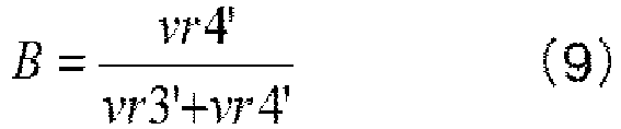
- the resistance values of the variable resistors VR3 and VR4 are changed to be vr3' and vr4' respectively, given the dividing ratio as B as shown in the below formula (9), the value of a comparative potential Vcmp2 is given by the below formula (10).
- the comparative potentials Vcmp1 and Vcmp2 respectively represent lines with gradients A and B.
- the gradient A is set to be higher than B.
- the reference potential Vref represents a horizontal line.
- the output of the comparator 5 is altered from the conducting potential to the interrupting potential, or vice versa, at the intersecting point of either line of the comparative potential Vcmp1 or Vcmp2 and the line of the reference potential Vref.
- the line of the comparative potential Vcmp1 which has a larger gradient than the comparative potential Vcmp2, intersects the line of the reference potential Vref when the input voltage Vin is Vlow, thereby altering the output of the comparator 5 from the conducting potential to the interrupting potential, or vice versa.
- the line of the comparative potential Vcmp2 intersects the line of the reference potential Vref when the input voltage Vin is Vhigh, thereby altering the output of the comparator 5 from the conducting potential to the interrupting potential, or vice versa.
- the input voltage control device 1B enables it to control power supply to various load devices adaptively to their input voltages Vin by regulating the resistance values of the variable resistor VR3 and the variable resistor VR4 in the comparative potential generator 4B.
- the comparative potential generator 4B may have one invariable resistor, instead of having the two variable resistors VR3 and VR4.
- Fig. 6 is a view showing an exemplary configuration of an input voltage control device 1C according to a third embodiment of the present invention.
- the input voltage control device 1C comprises a first power line L1, a second power line L2, a third power line L3, a smoothing condenser C1, a constant voltage generator 2, a reference potential generator 3B, a comparative potential generator 4C, a comparator 5, hysteresis resistor R5, an NMOS transistor 6 (a semiconductor device), a transformer 7, a resistor R6 and a diode D1.
- the input voltage control device 1C differs from the input voltage control device 1B of the second embodiment in the configuration of the comparative potential generator 4C.
- Other members of the input voltage control device 1C are configured in the same way as those of the input voltage control device 1B.
- the comparative potential generator 4C is connected to the first power line L1 and the one line of the second power line L2.
- the comparative potential generator 4C has a resistor R3, a Zener diode ZD and a resistor R4.
- the resistor R3 has an end connected to the first power line L1 and the other end connected to the cathode of the Zener diode ZD.
- the Zener diode ZD has its anode connected to an end of the resistor R4.
- the resistor R4 has the other end connected to the one line of the second power line L2.
- the potential difference between the first potential V1 and the second potential V2 (or input voltage Vin) is variable.
- the Zener diode ZD is a voltage sharing device which shares voltage equivalent to its Zener voltage (or breakdown voltage) .
- the Zener diode ZD lowers the input voltage Vin by the voltage equivalent to its Zener voltage.
- the resistors R3 and R4 divide the lowered input voltage Vin so as to generate a comparative voltage Vcmp (voltage of 0V to 24V, for example) which is within the range of the potential difference between the third potential V3 and the first potential V1.
- the comparative potential generator 4C outputs the comparative voltage Vcmp.
- Fig. 7 is a view showing an example of the relationship between the input voltage, the reference potential and the comparative potential in the input voltage control device 1C shown in Fig. 6 .
- the value of the comparative potential Vcmp is given by proportionally dividing the value of the input voltage Vin as shown in the above formula (2).
- the value of a comparative potential Vcmp3 ignoring the existence of the Zener diode ZD, is given by the below formula (11) following the above formula (4).
- the Zener voltage of the Zener diode ZD is Vzd
- the value of a comparative potential Vcmp4 when the Zener diode ZD exists, is given by the below formula (12).
- the comparative potentials Vcmp3 and Vcmp4 each represents a line with a gradient a.
- the line of the comparative potential Vcmp4 is horizontally shifted to the higher side on the axis Vin by the voltage equivalent to the Zener voltage Vzd.
- the reference potential Vref represents a horizontal line. Ignoring the existence of the hysteresis resistor R5 , the output of the comparator 5 is altered from the conducting potential to the interrupting potential, or vice versa, at the intersecting point of either line of the comparative potential Vcmp3 or Vcmp4 and the line of the reference potential Vref.
- the line of the comparative potential Vcmp3 intersects the line of the reference potential Vref when the input voltage Vin is Vlow, thereby altering the output of the comparator 5 from the conducting potential to the interrupting potential, or vice versa.
- the line of the comparative potential Vcmp4 intersects the line of the reference potential Vref when the input voltage Vin is Vhigh, thereby altering the output of the comparator 5 from the conducting potential to the interrupting potential, or vice versa.
- the input voltage control device 1C enables it to control power supply to various load devices adaptively to their input voltages Vin by regulating the Zener voltage Vzd of the Zener diode ZD in the comparative potential generator 4C.
- a set of directly connected Zener diodes is capable of sharing higher voltage.
- a set of two Zener diodes directly connected each having a Zener voltage of 100V is capable of sharing voltage of 200V.
- a shunt regulator may be used as a voltage sharing device which allows change in the sharing voltage.
- the NMOS transistor 6 is disposed between the one line an the other line of the second power line L2.
- the first power line L1 in stead of the second power line L2, may be divided into two lines and a PMOS transistor may be disposed between the one line an the other line of the first power line L1.
- the current path of the PMOS transistor (between the source and the drain) is turned conductive by inputting to its gate electrode a potential lower by a predetermined voltage than that of the first power line L1, and the current path is turned non-conductive by inputting to its gate electrode a potential equivalent to that of the first power line L1.
- the second power line L2 and the first power line L1 respectively correspond to the first power line and the second power line in the present invention.
- a reference potential generator 3A or 3B, a comparative potential generator 4A, 4B or 4C, a comparator 5 and a hysteresis resistor R5 are integrated into a DSP (Digital Signal Processor) and its control program, with the potential difference between the potential V1 of the first power line L1 and the potential V2 of the second power line L2 (or input voltage Vin) being AD-converted to digital signal.
- DSP Digital Signal Processor
- the input voltage control device is capable of controlling power supply to each load device based on the voltage level of the DC bus.
- the input voltage control device can be designed to supply power to load devices with low importance such as lighting devices when the voltage of the DC bus is 380V or higher and to stop supplying power when the voltage of the DC bus is less than 380V.
- the input voltage control device can be designed to supply power to load devices with high importance such as computers when the voltage of the DC bus is 300V or higher and to stop supplying power when the voltage of the DC bus is less than 300V.
Landscapes
- Engineering & Computer Science (AREA)
- Power Engineering (AREA)
- Physics & Mathematics (AREA)
- General Physics & Mathematics (AREA)
- Theoretical Computer Science (AREA)
- Automation & Control Theory (AREA)
- General Engineering & Computer Science (AREA)
- Electromagnetism (AREA)
- Radar, Positioning & Navigation (AREA)
- Dc-Dc Converters (AREA)
- Continuous-Control Power Sources That Use Transistors (AREA)
- Direct Current Feeding And Distribution (AREA)
Abstract
Description
- The present invention relates to an input voltage control device used in a system comprising a DC bus and load devices each connected thereto, the input voltage control device being disposed between the DC bus and each load device so as to control supply of input voltage to each load device.
- Patent Document 1 discloses a distributed power supply system in which multiple variable power generators and multiple load devices are connected to a DC bus. The variable power generators used in the system are, for example, photovoltaic power generators and wind power generators. When the voltage of the DC bus is lowered, the system selectively cuts off power supply to the selected load devices with low importance in a step-by-step-manner according to the voltage level of the DC bus.
- On the other hand, with an aim to apply to the smart grid, research and development has been conducted on HVDC (High Voltage Direct Current) power transmission at a voltage level of about 380V. In such a large-scale power transmission system, it is desirable that each of the load devices autonomously control supply of input voltage to itself.
- For example,
Patent Document 2 disclose a voltage conversion device which is capable of, when detecting drop of input voltage to its voltage conversion circuit, decreasing supply of input current to the voltage conversion circuit so as to lower power supplied to a load device by the voltage conversion circuit. -
- Patent Document 1: Japanese Patent Laid-open No.
2003-339118 - Patent Document 2: Japanese Patent Laid-open No.
2013-126277 - Patent Document 1 teaches selecting load devices with low importance according to the voltage level of the DC bus and cutting off power supply to the selected load devices in a step- by- step- manner. However, it does not teach any concrete measure.
-
Patent Document 2 teaches a voltage conversion device which decreases supply of power to the load device in response to the drop of the voltage level of the DC bus. However, it is not desirable to gradually decrease power supply to some kind of load devices, such as computers. - In consideration of the above problems of the prior art systems, it is an object of the present invention to provide an input voltage control device used in a system comprising a DC bus and load devices each connected thereto, the input voltage control device being disposed between the DC bus and each load device and capable of controlling power supply to each load device based on the voltage level of the DC bus.
- As a solution to the above- mentioned problems, the present invention has been accomplished, the details of which are described bellow.
- According to the present invention, there is provided
- Preferably, the input voltage control device according to the present invention system of the present invention is further characterized in that
- Preferably, the input voltage control device according to the present invention system of the present invention is further characterized in that
- Preferably, the input voltage control device according to the present invention system of the present invention is further characterized in that
- Preferably, the input voltage control device according to the present invention system of the present invention is further characterized in that
- The input voltage control device according to the present invention is capable of controlling power supply to each load device based on the voltage level of the DC bus.
-
-
Fig. 1 is a view showing an exemplary configuration of an input voltage control device according to a first embodiment of the present invention. -
Fig. 2 is a view showing an example of relationship between an input voltage, a reference potential and a comparative potential in the input voltage control device shown inFig. 1 . -
Fig. 3 is a view showing an exemplary configuration of a constant voltage generator. -
Fig. 4 is a view showing an exemplary configuration of an input voltage control device according to a second embodiment of the present invention. -
Fig. 5 is a view showing an example of relationship between an input voltage, a reference potential and a comparative potential in the input voltage control device shown inFig. 4 . -
Fig. 6 is a view showing an exemplary configuration of an input voltage control device according to a third embodiment of the present invention. -
Fig. 7 is a view showing an example of relationship between an input voltage, a reference potential and a comparative potential in the input voltage control device shown inFig. 6 . - Described hereinafter with reference to the attached drawings are detailed embodiments of the input voltage control device according to the present invention. Throughout the figures illustrating exemplary embodiments of the present invention, like reference numerals refer to like members which have similar basic composition and operation.
-
Fig. 1 is a view showing an exemplary configuration of an inputvoltage control device 1A according to a first embodiment of the present invention. - The input
voltage control device 1A comprises a first power line L1, a second power line L2, a third power line L3, a smoothing condenser C1, aconstant voltage generator 2, a referencepotential generator 3A, a comparativepotential generator 4A, acomparator 5, hysteresis resistor R5, an NMOS transistor 6 (which is a semiconductor device), atransformer 7, a resistor R6 and a diode D1. - The first power line L1 is connected to a terminal T1 and a terminal T3.
- The second power line L2 is divided into one line and the other line, having the
NMOS transistor 6 therebetween. The one line of the second power line L2 is connected to a terminal T2 and the source electrode of theNMOS transistor 6. - The other line of the second power line L2 is connected to the drain electrode of the
NMOS transistor 6 and a terminal T2. - As shown in
Fig. 1 , the inputvoltage control device 1A has thetransformer 7 and the diode D1 disposed in parallel alignment on the other line of the second power line L2. One end of the primary coil of thetransformer 7 and the anode of the diode D1 are connected to the drain electrode (D) of theNMOS transistor 6. The other end of the primary coil of thetransformer 7 and the cathode of the diode D1 are connected to the terminal T4. The both ends of the secondary coil of thetransformer 7 are connected to the resistor R6 to form a loop. - Configured as in the above, the diode D1 suppresses counter voltage generated when the
NMOS transistor 6 is turned off. The mutual induction of thetransformer 7 and the resistor restricts current and magnetic saturation when theNMOS transistor 6 is turned on. Thus, the resistor R6 decides the degree of mitigating inrush current to load devices. After inrush current is settled, mutual induction does not occur in thetransformer 7, Since thetransformer 7 only has coil resistance (almost 0 ohm), it does not cause power loss. - The terminals T1 and T2 are connected to an external DC bus, which is, for example, a part of a high voltage direct current power transmission system. To the terminal T1 is applied a first potential V1. To the terminal T2 is applied a second potential V2. The potential difference between the first potential V1 and the second potential V2 is defined as an input voltage Vin. In one example, the first potential V1 is set to be 380V and the second potential V2 is set to be 0V. In another example, the first potential V1 is set to be 190V and the second potential V2 is set to be -190V. The potentials V1 and V2 (the input voltage Vin) applied to the terminals T1 and T2 are variable.
- The terminals T3 and T4 are connected to a load device. The load device may be of various kinds including normal lighting devices, emergency lighting devices, air conditioners, computers and manufacturing devices.
- The smoothing condenser C1 has its one end and the other end respectively connected to the first power line L1 and second power line L2. The smoothing condenser C1 smoothes fluctuation of the input voltage Vin.
- The
constant voltage generator 2 operates on the voltage supplied by the first power line L1 and the one line of the second power line L2 (the input voltage Vin) and outputs a third potential V3 from its output terminal (Out) to the third power line L3. The output voltage of theconstant voltage generator 2, which is equal to the potential difference between the third potential V3 and the second potential V2 (voltage of 24V, for example), is constant and stable. An exemplary configuration of theconstant voltage generator 2 will be described in detail with reference toFig. 3 afterwards. - The
reference potential generator 3A is connected to the third power line L3 and the one line of the second power line L2. Thereference potential generator 3A has variable resistors VR1 and VR2. The variable resistor VR1 has an end connected to the third power line L3 and the other end connected to an end of the variable resistor VR2. The variable resistor VR2 has the other end connected to the one line of the second power line L2. Thereference potential generator 3A divides the potential difference (or voltage) between the third potential V3 and the second potential V2 by means of the variable resistors VR1 and VR2 so as to generate and output a reference potential Vref. - The comparative
potential generator 4A is connected to the first power line L1 and the one line of the second power line L2. The comparativepotential generator 4A has resistors R3 and R4. The resistor R3 has an end connected to the first power line L1 and the other end connected to an end of the resistor R4. The resistor R4 has the other end connected to the one line of the second power line L2. The potential difference between the first potential V1 and the second potential V2 (or input voltage Vin) is variable. The comparativepotential generator 4A divides the input voltage Vin by means of the resistors R3 and R4 so as to generate and output a comparative voltage Vcmp (voltage of 0V to 24V, for example) which is within the range of the potential difference between the third potential V3 and the first potential V1. - The
comparator 5 operates on the voltage (the potential difference between the third potential V3 and the second potential V2, for example, voltage of 24V) supplied by the third power line L3 and the one line of the second power line L2. Thecomparator 5 has an inverted input terminal, to which the reference potential Vref outputted from thereference potential generator 3A is inputted. Thecomparator 5 has a non-inverted input terminal, to which the comparative voltage Vcmp outputted from the comparativepotential generator 4A is inputted. Thecomparator 5 outputs a conducting potential (voltage of 24V, for example) or an interrupting potential (voltage of 0V, for example) depending on the comparison between the reference potential Vref and the comparative potential Vcmp. - The output terminal and the non-inverted input terminal are connected to each terminal of the hysteresis resistor R5. The hysteresis resistor R5 imparts hysteresis to the output of the
comparator 5. If the hysteresis resistor R5 is not present, thecomparator 5 outputs the conducting potential when the comparative potential Vcmp is higher than the reference potential Vref and the interrupting potential when the comparative potential Vcmp is lower than the reference potential Vref. However, by the effects of hysteresis, the comparative potential Vcmp which was higher than the reference potential Vref gradually drops and when the comparative potential Vcmp becomes lower than the reference potential Vref to a certain degree, thecomparator 5 alters its output from the conducting potential to the interrupting potential. On the other hand, the comparative potential Vcmp which was lower than the reference potential Vref gradually raises and when the comparative potential Vcmp becomes higher than the reference potential Vref to a certain degree, thecomparator 5 alters its output from the interrupting potential to the conducting potential. - As described in the above, the source electrode of the
NMOS transistor 6 is connected to the one line of the second power line L2 and the drain electrode to the other line of the second power line L2. The gate electrode of theNMOS transistor 6 is connected to the output end of thecomparator 5. TheNMOS transistor 6 allows the source-drain current path to conduct when a conducting potential (voltage of 24V, for example) is inputted to its gate electrode, thereby supplying power to the load device connected to the terminals T3 and T4. TheNMOS transistor 6 interrupts the source-drain current path when an interrupting potential (voltage of 0V, for example) is inputted to its gate electrode, thereby interrupting power supply to the load device. -
Fig. 2 is a view showing an example of the relationship between the input voltage Vin, the reference potential Vref and the comparative potential Vcmp in the inputvoltage control device 1A shown inFig. 1 . - Assuming the resistance values of the variable resistors VR1 and VR2 as vr1 and vr2 respectively, the value of the reference potential Vref is given by the below formula (1).
[Formula 1]
- On the other hand, assuming the resistance values of the resistors R3 and R4 as r3 and r4 respectively, the value of the comparative potential Vcmp is given by proportionally dividing the value of the input voltage Vin as shown in the below formula (2). Given the dividing ratio as a as shown in the below formula (3), the value of the comparative potential Vcmp is given by the below formula (4).
[Formula 2]


- As shown in
Fig. 2 , the comparative potential Vcmp represents a line with a gradient a. On the other hand, although the reference potential Vref represents a horizontal line, its value is variable according to the change in the resistance value of vr1 and vr2. - Ignoring the existence of the hysteresis resistor R5, the output of the
comparator 5 is altered from the conducting potential to the interrupting potential , or vice versa, at the intersecting point of the line of the comparative potential Vcmp and the line of the reference potential Vref. For example, in case the reference potential Vref is set to be a higher value, the output of thecomparator 5 is altered from the conducting potential to the interrupting potential, or vice versa, at the time when the input voltage Vin becomes Vhigh. On the other hand, in case the reference potential Vref is set to be a lower value, the output of thecomparator 5 is altered from the conducting potential to the interrupting potential, or vice versa, at the time when the input voltage Vin becomes Vlow. - As described in the above, the input
voltage control device 1A according to the first embodiment of the present invention enables it to control power supply to various load devices adaptively to their input voltages Vin by regulating the resistance values of the variable resistor VR1 and the variable resistor VR2 in thereference potential generator 3A. - The
reference potential generator 3A may have one invariable resistor, instead of having the two variable resistors VR1 and VR2. -
Fig. 3 is a view showing an exemplary configuration of theconstant voltage generator 2. - The
constant voltage generator 2 comprises Zener diodes Z20 and Z21, NPN transistors Tr20 and Tr21, a resistors R20, R21 and R22, and a condenser C20. - The Zener diode Z20 has its anode connected to the second power line L2 and its cathode connected to an end of the resistor R21. The resistor R21 has the other end connected to the first power line L1.
- The NPN transistors Tr20 and Tr21 are Darlington connected.
- The NPN transistor Tr20 has its base connected to the cathode of the Zener diode Z20 and an end of the resistor R21. The NPN transistor Tr20 has its emitter connected to the output terminal Out through the resistor R22. The NPN transistor Tr21 has its emitter connected to the output terminal Out.
- The NPN transistor Tr20 has its collector connected to an end of the resistor R20. The NPN transistor Tr21 has its collector connected to an end of the resistor R20. The resistor R20 has the other end connected to the first power line L1. The resistor R20 is mounted externally to the input
voltage control device 1A so as to radiate its heat. - The Zener diode Z21 has its anode connected to the output terminal Out and its cathode connected to the cathode of the Zener diode Z20 and an end of the resistor R21.
- The condenser C20 has its one end connected to the second power line L2 and the other end connected to the output terminal Out.
- The
constant voltage generator 2 outputs a constant and stable voltage (voltage of 24V, for example) from its output terminal Out. -
Fig. 4 is a view showing an exemplary configuration of an inputvoltage control device 1B according to a second embodiment of the present invention. - The input
voltage control device 1B comprises a first power line L1, a second power line L2, a third power line L3, a smoothing condenser C1, aconstant voltage generator 2, a referencepotential generator 3B, a comparativepotential generator 4B, acomparator 5, hysteresis resistor R5, an NMOS transistor 6 (which is a semiconductor device), atransformer 7, a resistor R6 and a diode D1. - The input
voltage control device 1B differs from the inputvoltage control device 1A of the first embodiment in the configuration of the referencepotential generator 3B and the comparativepotential generator 4B. Other members of the inputvoltage control device 1B are configured in the same way as those of the inputvoltage control device 1A. - The reference
potential generator 3B is connected to the third power line L3 and the one line of the second power line L2. The referencepotential generator 3B has resistors R1 and R2. The resistor R1 has an end connected to the third power line L3 and the other end connected to an end of the resistor R2. The resistor R2 has the other end connected to the one line of the second power line L2. The referencepotential generator 3B divides the potential difference (or voltage) between the third potential V3 and the second potential V2 by means of the resistors R1 and R2 so as to generate and output a reference potential Vref. - The comparative
potential generator 4B is connected to the first power line L1 and the one line of the second power line L2. The comparativepotential generator 4B has variable resistors VR3 and VR4. The variable resistor VR3 has an end connected to the first power line L1 and the other end connected to an end of the variable resistor VR4. The variable resistor VR4 has the other end connected to the one line of the second power line L2. The potential difference between the first potential V1 and the second potential V2 (or input voltage Vin) is variable. The comparativepotential generator 4B divides the input voltage Vin by means of the variable resistors VR3 and VR4 so as to generate and output a comparative voltage Vcmp (voltage of 0V to 24V, for example) which is within the range of the potential difference between the third potential V3 and the first potential V1. -
Fig. 5 is a view showing an example of the relationship between the input voltage Vin, the reference potential Vref and the comparative potential Vcmp in the inputvoltage control device 1B shown inFig. 4 . - Assuming the resistance values of the resistors R1 and R2 as r1 and r2 respectively, the value of the reference potential Vref is given by the below formula (5).
[Formula 3]
- On the other hand, assuming that the resistance values of the variable resistors VR3 and VR4 are vr3 and vr4 respectively, the value of the comparative potential Vcmp is given by proportionally dividing the value of the input voltage Vin as shown in the below formula (6). Given the dividing ratio A as shown in the below formula (7), the value of a comparative potential Vcmp1 is given by the below formula (8). When the resistance values of the variable resistors VR3 and VR4 are changed to be vr3' and vr4' respectively, given the dividing ratio as B as shown in the below formula (9), the value of a comparative potential Vcmp2 is given by the below formula (10).
[Formula 4]



- As shown in
Fig. 5 , the comparative potentials Vcmp1 and Vcmp2 respectively represent lines with gradients A and B. The gradient A is set to be higher than B. On the other hand, the reference potential Vref represents a horizontal line. - Ignoring the existence of the hysteresis resistor R5 , the output of the
comparator 5 is altered from the conducting potential to the interrupting potential, or vice versa, at the intersecting point of either line of the comparative potential Vcmp1 or Vcmp2 and the line of the reference potential Vref. The line of the comparative potential Vcmp1, which has a larger gradient than the comparative potential Vcmp2, intersects the line of the reference potential Vref when the input voltage Vin is Vlow, thereby altering the output of thecomparator 5 from the conducting potential to the interrupting potential, or vice versa. On the other hand, the line of the comparative potential Vcmp2 intersects the line of the reference potential Vref when the input voltage Vin is Vhigh, thereby altering the output of thecomparator 5 from the conducting potential to the interrupting potential, or vice versa. - As described in the above, the input
voltage control device 1B according to the second embodiment of the present invention enables it to control power supply to various load devices adaptively to their input voltages Vin by regulating the resistance values of the variable resistor VR3 and the variable resistor VR4 in the comparativepotential generator 4B. - The comparative
potential generator 4B may have one invariable resistor, instead of having the two variable resistors VR3 and VR4. -
Fig. 6 is a view showing an exemplary configuration of an input voltage control device 1C according to a third embodiment of the present invention. - The input voltage control device 1C comprises a first power line L1, a second power line L2, a third power line L3, a smoothing condenser C1, a
constant voltage generator 2, a referencepotential generator 3B, a comparativepotential generator 4C, acomparator 5, hysteresis resistor R5, an NMOS transistor 6 (a semiconductor device), atransformer 7, a resistor R6 and a diode D1. - The input voltage control device 1C differs from the input
voltage control device 1B of the second embodiment in the configuration of the comparativepotential generator 4C. Other members of the input voltage control device 1C are configured in the same way as those of the inputvoltage control device 1B. - The comparative
potential generator 4C is connected to the first power line L1 and the one line of the second power line L2. The comparativepotential generator 4C has a resistor R3, a Zener diode ZD and a resistor R4. The resistor R3 has an end connected to the first power line L1 and the other end connected to the cathode of the Zener diode ZD. The Zener diode ZD has its anode connected to an end of the resistor R4. The resistor R4 has the other end connected to the one line of the second power line L2. The potential difference between the first potential V1 and the second potential V2 (or input voltage Vin) is variable. - The Zener diode ZD is a voltage sharing device which shares voltage equivalent to its Zener voltage (or breakdown voltage) . The Zener diode ZD lowers the input voltage Vin by the voltage equivalent to its Zener voltage. The resistors R3 and R4 divide the lowered input voltage Vin so as to generate a comparative voltage Vcmp (voltage of 0V to 24V, for example) which is within the range of the potential difference between the third potential V3 and the first potential V1. The comparative
potential generator 4C outputs the comparative voltage Vcmp. -
Fig. 7 is a view showing an example of the relationship between the input voltage, the reference potential and the comparative potential in the input voltage control device 1C shown inFig. 6 . - The value of the reference potential Vref is given by the above formula (5).
- On the other hand, assuming that the resistance values of the resistors R3 and R4 are vr3 and vr4 respectively, and ignoring the existence of the Zener diode ZD, the value of the comparative potential Vcmp is given by proportionally dividing the value of the input voltage Vin as shown in the above formula (2). Given the dividing ratio as a as shown in the above formula (3), the value of a comparative potential Vcmp3, ignoring the existence of the Zener diode ZD, is given by the below formula (11) following the above formula (4). Assuming that the Zener voltage of the Zener diode ZD is Vzd, the value of a comparative potential Vcmp4, when the Zener diode ZD exists, is given by the below formula (12).
[Formula 5]

- As shown in
Fig. 7 , the comparative potentials Vcmp3 and Vcmp4 each represents a line with a gradient a. The line of the comparative potential Vcmp4 is horizontally shifted to the higher side on the axis Vin by the voltage equivalent to the Zener voltage Vzd. On the other hand, the reference potential Vref represents a horizontal line. Ignoring the existence of the hysteresis resistor R5 , the output of thecomparator 5 is altered from the conducting potential to the interrupting potential, or vice versa, at the intersecting point of either line of the comparative potential Vcmp3 or Vcmp4 and the line of the reference potential Vref. The line of the comparative potential Vcmp3 intersects the line of the reference potential Vref when the input voltage Vin is Vlow, thereby altering the output of thecomparator 5 from the conducting potential to the interrupting potential, or vice versa. On the other hand, the line of the comparative potential Vcmp4 intersects the line of the reference potential Vref when the input voltage Vin is Vhigh, thereby altering the output of thecomparator 5 from the conducting potential to the interrupting potential, or vice versa. - As described in the above, the input voltage control device 1C according to the third embodiment of the present invention enables it to control power supply to various load devices adaptively to their input voltages Vin by regulating the Zener voltage Vzd of the Zener diode ZD in the comparative
potential generator 4C. - A set of directly connected Zener diodes is capable of sharing higher voltage. For example, a set of two Zener diodes directly connected each having a Zener voltage of 100V is capable of sharing voltage of 200V. In place of the Zener diodes, a shunt regulator may be used as a voltage sharing device which allows change in the sharing voltage.
- In the above- described embodiments, the
NMOS transistor 6 is disposed between the one line an the other line of the second power line L2. Alternatively, the first power line L1, in stead of the second power line L2, may be divided into two lines and a PMOS transistor may be disposed between the one line an the other line of the first power line L1. - In that case, the current path of the PMOS transistor (between the source and the drain) is turned conductive by inputting to its gate electrode a potential lower by a predetermined voltage than that of the first power line L1, and the current path is turned non-conductive by inputting to its gate electrode a potential equivalent to that of the first power line L1.
- Also, in that case, the second power line L2 and the first power line L1 respectively correspond to the first power line and the second power line in the present invention.
- It is possible to the configure the device such that a
reference potential generator potential generator comparator 5 and a hysteresis resistor R5 are integrated into a DSP (Digital Signal Processor) and its control program, with the potential difference between the potential V1 of the first power line L1 and the potential V2 of the second power line L2 (or input voltage Vin) being AD-converted to digital signal. - As described in the above, the input voltage control device according to the present invention is capable of controlling power supply to each load device based on the voltage level of the DC bus.
- For example, the input voltage control device according to the present invention can be designed to supply power to load devices with low importance such as lighting devices when the voltage of the DC bus is 380V or higher and to stop supplying power when the voltage of the DC bus is less than 380V. On the other hand, the input voltage control device according to the present invention can be designed to supply power to load devices with high importance such as computers when the voltage of the DC bus is 300V or higher and to stop supplying power when the voltage of the DC bus is less than 300V.
- In the above- described embodiments of the present invention, various modifications and combinations may be made for convenience of design and other reasons within the scope of the claimed inventions or the inventions described herein.
-
- 1A, 1B, 1C
- input voltage control device
- 2
- constant voltage generator
- 3A, 3B
- reference potential generator
- 4A, 4B, 4C
- comparative potential generator
- 5
- comparator
- 6
- NMOS transistor
- 7
- transformer
- L1
- first power line
- L2
- second power line
- L3
- third power line
- C1
- smoothing condenser
- R1, R2, R3, R4, R6
- resistor
- R5
- hysteresis resistor
- VR1, VR2, VR3, VR4
- variable resistor
- ZD
- Zener diode
- D1
- diode
Claims (5)
- An input voltage control device comprising:a first power line to which a first potential is applied;a second power line divided into one part and the other part, to said one part a second potential being applied to;a third power line;a constant voltage generator operating on the first potential supplied by said first power line and the second potential supplied by said one part of the second power line and outputting to said third power line a third potential having a constant potential difference from said second potential;a reference potential generator connected to said third power line and said one part of the second power line, generating a reference potential on the basis of said third potential and said second potential and outputting said reference potential;a comparative potential generator connected to said first power line and said one part of the second power line, generating a comparative potential on the basis of said first potential and said second potential and outputting said comparative potential;a comparator operating on the third potential supplied by said third power line and the second potential supplied by said one part of the second power line and alternately outputting a conducting potential or an interrupting potential depending on the comparison between said reference potential and said comparative potential; anda semiconductor device with one terminal of its current path connected to said one part of the second power line, the other terminal connected to said other part of the second power line and a control terminal connected to the output terminal of said comparator, the semiconductor device making said current path conductive when the conducting potential is inputted to said control terminal and non- conductive when the interrupting potential is inputted to said control terminal.
- The input voltage control device as set forth in Claim 1, wherein said reference potential generator comprises at least one variable resistor and is capable of changing the reference potential by changing the resistance value of said at least one variable resistor.
- The input voltage control device as set forth in Claim 1, wherein said comparative potential generator comprises at least one variable resistor and is capable of changing the comparative potential by changing the resistance value of said at least one variable resistor.
- The input voltage control device as set forth in Claim 1, wherein said comparative potential generator comprises a voltage sharing device for lowering the potential difference between said first potential supplied by said first power line and said second potential supplied by said one part of the second power line, thereby generating a comparative potential on the basis of the lowered potential difference.
- The input voltage control device as set forth in any one of Claims 1 to 4, wherein said semiconductor device is an NMOS transistor and said comparative potential and said reference potential are respectably inputted to the non- inverted input terminal and the inverted input terminal of said comparator.
Applications Claiming Priority (2)
| Application Number | Priority Date | Filing Date | Title |
|---|---|---|---|
| JP2016055821A JP6641208B2 (en) | 2016-03-18 | 2016-03-18 | Input voltage controller |
| PCT/JP2017/009476 WO2017159536A1 (en) | 2016-03-18 | 2017-03-09 | Input voltage control device |
Publications (3)
| Publication Number | Publication Date |
|---|---|
| EP3432435A1 true EP3432435A1 (en) | 2019-01-23 |
| EP3432435A4 EP3432435A4 (en) | 2019-11-13 |
| EP3432435B1 EP3432435B1 (en) | 2020-10-07 |
Family
ID=59851490
Family Applications (1)
| Application Number | Title | Priority Date | Filing Date |
|---|---|---|---|
| EP17766537.9A Not-in-force EP3432435B1 (en) | 2016-03-18 | 2017-03-09 | Input voltage control device |
Country Status (6)
| Country | Link |
|---|---|
| US (1) | US10528072B2 (en) |
| EP (1) | EP3432435B1 (en) |
| JP (1) | JP6641208B2 (en) |
| KR (1) | KR20180124022A (en) |
| CN (1) | CN109075570A (en) |
| WO (1) | WO2017159536A1 (en) |
Families Citing this family (2)
| Publication number | Priority date | Publication date | Assignee | Title |
|---|---|---|---|---|
| JP6694300B2 (en) * | 2016-03-22 | 2020-05-13 | Ntn株式会社 | Control signal generation circuit |
| CN114442715B (en) * | 2021-12-29 | 2023-08-18 | 中国航空工业集团公司西安航空计算技术研究所 | 28V or open circuit discrete quantity output circuit |
Family Cites Families (25)
| Publication number | Priority date | Publication date | Assignee | Title |
|---|---|---|---|---|
| US4479174A (en) * | 1982-11-03 | 1984-10-23 | Reliance Electric Company | Efficiency increasing circuit for switching power supplies operating at low power levels |
| US5754414A (en) * | 1996-02-23 | 1998-05-19 | Hanington; Gary J. | Self-compensating switching power converter |
| JP2002112469A (en) * | 2000-09-29 | 2002-04-12 | Allied Tereshisu Kk | Or circuit consisting of field-effect transistors and power supply using it |
| JP4219567B2 (en) * | 2001-04-03 | 2009-02-04 | 三菱電機株式会社 | Semiconductor device |
| JP2003339118A (en) | 2002-05-22 | 2003-11-28 | My Way Giken Kk | Distributed power supply system |
| US7508176B2 (en) * | 2004-05-14 | 2009-03-24 | O2Micro International Limited | Controller for a DC to DC converter having linear mode and switch mode capabilities |
| DE112005000026T5 (en) * | 2004-07-01 | 2006-07-27 | Murata Mfg. Co., Ltd., Nagaokakyo | DC-DC converter and converter device |
| JP4302070B2 (en) * | 2005-02-25 | 2009-07-22 | Okiセミコンダクタ株式会社 | Power supply switching circuit, microcomputer, portable terminal device, and power supply switching control method |
| JP4948846B2 (en) * | 2006-02-08 | 2012-06-06 | 株式会社東芝 | Power supply device with inrush current suppression circuit |
| JP4868918B2 (en) * | 2006-04-05 | 2012-02-01 | 株式会社東芝 | Reference voltage generator |
| TWI554030B (en) * | 2010-10-20 | 2016-10-11 | 羅姆股份有限公司 | High-voltage side switch circuit, interface circuit and electronic machine |
| JP5516320B2 (en) * | 2010-10-21 | 2014-06-11 | ミツミ電機株式会社 | Semiconductor integrated circuit for regulator |
| CN102063143B (en) * | 2010-11-10 | 2012-10-31 | 中国兵器工业集团第二一四研究所苏州研发中心 | A slowly changing power management circuit |
| JP5797106B2 (en) | 2011-12-14 | 2015-10-21 | エヌ・ティ・ティ・データ先端技術株式会社 | Voltage converter and power supply subordinate control system |
| JP5762358B2 (en) * | 2012-06-04 | 2015-08-12 | 旭化成エレクトロニクス株式会社 | DC power supply |
| JP5988214B2 (en) * | 2012-12-04 | 2016-09-07 | パナソニックIpマネジメント株式会社 | Lighting device and lighting apparatus using the same |
| WO2014129126A1 (en) * | 2013-02-20 | 2014-08-28 | パナソニック株式会社 | Switching power supply apparatus |
| CN104035827A (en) * | 2013-03-08 | 2014-09-10 | 鸿富锦精密工业(深圳)有限公司 | Electronic device |
| JP2015011505A (en) * | 2013-06-28 | 2015-01-19 | ソニー株式会社 | Voltage detector, electronic device, and control method of voltage detector |
| JP2015172904A (en) * | 2014-03-12 | 2015-10-01 | 株式会社東芝 | LDO voltage regulator and power receiving device |
| US9509216B2 (en) * | 2014-07-04 | 2016-11-29 | Rohm Co., Ltd. | Switching power supply circuit |
| CN104219842B (en) * | 2014-08-29 | 2017-09-29 | 深圳市奋勇光电有限公司 | Led constant current device |
| JP6718109B2 (en) * | 2016-03-07 | 2020-07-08 | 富士通株式会社 | Overvoltage protection circuit and overvoltage protection control method |
| JP2018014561A (en) * | 2016-07-19 | 2018-01-25 | 富士電機株式会社 | Semiconductor device |
| JP2019047621A (en) * | 2017-09-01 | 2019-03-22 | ミツミ電機株式会社 | Semiconductor device for power supply control, power supply device, and discharge method of x capacitor |
-
2016
- 2016-03-18 JP JP2016055821A patent/JP6641208B2/en not_active Expired - Fee Related
-
2017
- 2017-03-09 CN CN201780013828.2A patent/CN109075570A/en active Pending
- 2017-03-09 EP EP17766537.9A patent/EP3432435B1/en not_active Not-in-force
- 2017-03-09 WO PCT/JP2017/009476 patent/WO2017159536A1/en not_active Ceased
- 2017-03-09 KR KR1020187022492A patent/KR20180124022A/en not_active Abandoned
- 2017-03-09 US US16/086,242 patent/US10528072B2/en not_active Expired - Fee Related
Also Published As
| Publication number | Publication date |
|---|---|
| EP3432435A4 (en) | 2019-11-13 |
| JP2017175677A (en) | 2017-09-28 |
| EP3432435B1 (en) | 2020-10-07 |
| KR20180124022A (en) | 2018-11-20 |
| US20190165574A1 (en) | 2019-05-30 |
| WO2017159536A1 (en) | 2017-09-21 |
| CN109075570A (en) | 2018-12-21 |
| JP6641208B2 (en) | 2020-02-05 |
| US10528072B2 (en) | 2020-01-07 |
Similar Documents
| Publication | Publication Date | Title |
|---|---|---|
| US9007737B2 (en) | Overvoltage protection circuit and method thereof | |
| CN109861329B (en) | Linear charging system, constant-current constant-voltage control circuit and voltage following control method thereof | |
| CN107580390B (en) | LED lamp | |
| EP3432435B1 (en) | Input voltage control device | |
| US10609799B2 (en) | Multi-output dimmable class-2 power supply in accord with american standard | |
| JP2013196704A (en) | Constant voltage generation circuit and constant voltage generation method | |
| US20150084502A1 (en) | Voltage Supply for Electrical Focusing of Electron Beams | |
| CN205644338U (en) | Lower electric time sequence control circuit and circuit control system | |
| JP2017123091A (en) | regulator | |
| US11841721B2 (en) | Voltage regulator and in-vehicle backup power supply | |
| TWI685167B (en) | Current regulation system | |
| CN110971108B (en) | Transformer secondary output circuit, switching power supply circuit, air conditioner | |
| CN107005162B (en) | DC voltage converter systems, DC voltage supply systems and printed circuit boards for DC voltage converter systems | |
| CN103828205B (en) | For controlling the power supply of power switch | |
| CN205608579U (en) | High pressure resistant linear voltage regulator based on standard CMOS technology | |
| CN105786073B (en) | A kind of power-control device | |
| EP3540931A1 (en) | Voltage converter | |
| JP2015139321A (en) | Reference voltage output circuit and power supply device | |
| CN208888684U (en) | A kind of voltage-controlled power supply | |
| CN102736655B (en) | Linear voltage stabilizing circuit | |
| CN110502060B (en) | Constant current starting circuit | |
| US11528055B2 (en) | Method for generating low-frequency power carrier control signal | |
| CN221652817U (en) | Circuit arrangement for operating a semiconductor light source in dependence on a supply voltage | |
| JP6694300B2 (en) | Control signal generation circuit | |
| CN109189143A (en) | A kind of voltage-controlled power supply |
Legal Events
| Date | Code | Title | Description |
|---|---|---|---|
| STAA | Information on the status of an ep patent application or granted ep patent |
Free format text: STATUS: THE INTERNATIONAL PUBLICATION HAS BEEN MADE |
|
| PUAI | Public reference made under article 153(3) epc to a published international application that has entered the european phase |
Free format text: ORIGINAL CODE: 0009012 |
|
| STAA | Information on the status of an ep patent application or granted ep patent |
Free format text: STATUS: REQUEST FOR EXAMINATION WAS MADE |
|
| 17P | Request for examination filed |
Effective date: 20181017 |
|
| AK | Designated contracting states |
Kind code of ref document: A1 Designated state(s): AL AT BE BG CH CY CZ DE DK EE ES FI FR GB GR HR HU IE IS IT LI LT LU LV MC MK MT NL NO PL PT RO RS SE SI SK SM TR |
|
| AX | Request for extension of the european patent |
Extension state: BA ME |
|
| DAV | Request for validation of the european patent (deleted) | ||
| DAX | Request for extension of the european patent (deleted) | ||
| A4 | Supplementary search report drawn up and despatched |
Effective date: 20191015 |
|
| RIC1 | Information provided on ipc code assigned before grant |
Ipc: H02J 1/00 20060101AFI20191009BHEP Ipc: H02J 3/36 20060101ALI20191009BHEP Ipc: G06F 1/26 20060101ALI20191009BHEP Ipc: H02J 5/00 20160101ALI20191009BHEP |
|
| GRAP | Despatch of communication of intention to grant a patent |
Free format text: ORIGINAL CODE: EPIDOSNIGR1 |
|
| STAA | Information on the status of an ep patent application or granted ep patent |
Free format text: STATUS: GRANT OF PATENT IS INTENDED |
|
| RIC1 | Information provided on ipc code assigned before grant |
Ipc: H02J 5/00 20160101ALI20200406BHEP Ipc: H02J 1/00 20060101AFI20200406BHEP Ipc: H02J 3/36 20060101ALI20200406BHEP Ipc: G06F 1/26 20060101ALI20200406BHEP |
|
| INTG | Intention to grant announced |
Effective date: 20200423 |
|
| GRAS | Grant fee paid |
Free format text: ORIGINAL CODE: EPIDOSNIGR3 |
|
| GRAA | (expected) grant |
Free format text: ORIGINAL CODE: 0009210 |
|
| STAA | Information on the status of an ep patent application or granted ep patent |
Free format text: STATUS: THE PATENT HAS BEEN GRANTED |
|
| AK | Designated contracting states |
Kind code of ref document: B1 Designated state(s): AL AT BE BG CH CY CZ DE DK EE ES FI FR GB GR HR HU IE IS IT LI LT LU LV MC MK MT NL NO PL PT RO RS SE SI SK SM TR |
|
| REG | Reference to a national code |
Ref country code: GB Ref legal event code: FG4D |
|
| REG | Reference to a national code |
Ref country code: CH Ref legal event code: EP Ref country code: AT Ref legal event code: REF Ref document number: 1322181 Country of ref document: AT Kind code of ref document: T Effective date: 20201015 |
|
| REG | Reference to a national code |
Ref country code: IE Ref legal event code: FG4D |
|
| REG | Reference to a national code |
Ref country code: DE Ref legal event code: R096 Ref document number: 602017025118 Country of ref document: DE |
|
| REG | Reference to a national code |
Ref country code: NL Ref legal event code: MP Effective date: 20201007 |
|
| REG | Reference to a national code |
Ref country code: AT Ref legal event code: MK05 Ref document number: 1322181 Country of ref document: AT Kind code of ref document: T Effective date: 20201007 |
|
| PG25 | Lapsed in a contracting state [announced via postgrant information from national office to epo] |
Ref country code: FI Free format text: LAPSE BECAUSE OF FAILURE TO SUBMIT A TRANSLATION OF THE DESCRIPTION OR TO PAY THE FEE WITHIN THE PRESCRIBED TIME-LIMIT Effective date: 20201007 Ref country code: GR Free format text: LAPSE BECAUSE OF FAILURE TO SUBMIT A TRANSLATION OF THE DESCRIPTION OR TO PAY THE FEE WITHIN THE PRESCRIBED TIME-LIMIT Effective date: 20210108 Ref country code: PT Free format text: LAPSE BECAUSE OF FAILURE TO SUBMIT A TRANSLATION OF THE DESCRIPTION OR TO PAY THE FEE WITHIN THE PRESCRIBED TIME-LIMIT Effective date: 20210208 Ref country code: RS Free format text: LAPSE BECAUSE OF FAILURE TO SUBMIT A TRANSLATION OF THE DESCRIPTION OR TO PAY THE FEE WITHIN THE PRESCRIBED TIME-LIMIT Effective date: 20201007 Ref country code: NO Free format text: LAPSE BECAUSE OF FAILURE TO SUBMIT A TRANSLATION OF THE DESCRIPTION OR TO PAY THE FEE WITHIN THE PRESCRIBED TIME-LIMIT Effective date: 20210107 |
|
| REG | Reference to a national code |
Ref country code: LT Ref legal event code: MG4D |
|
| PG25 | Lapsed in a contracting state [announced via postgrant information from national office to epo] |
Ref country code: AT Free format text: LAPSE BECAUSE OF FAILURE TO SUBMIT A TRANSLATION OF THE DESCRIPTION OR TO PAY THE FEE WITHIN THE PRESCRIBED TIME-LIMIT Effective date: 20201007 Ref country code: ES Free format text: LAPSE BECAUSE OF FAILURE TO SUBMIT A TRANSLATION OF THE DESCRIPTION OR TO PAY THE FEE WITHIN THE PRESCRIBED TIME-LIMIT Effective date: 20201007 Ref country code: SE Free format text: LAPSE BECAUSE OF FAILURE TO SUBMIT A TRANSLATION OF THE DESCRIPTION OR TO PAY THE FEE WITHIN THE PRESCRIBED TIME-LIMIT Effective date: 20201007 Ref country code: PL Free format text: LAPSE BECAUSE OF FAILURE TO SUBMIT A TRANSLATION OF THE DESCRIPTION OR TO PAY THE FEE WITHIN THE PRESCRIBED TIME-LIMIT Effective date: 20201007 Ref country code: IS Free format text: LAPSE BECAUSE OF FAILURE TO SUBMIT A TRANSLATION OF THE DESCRIPTION OR TO PAY THE FEE WITHIN THE PRESCRIBED TIME-LIMIT Effective date: 20210207 Ref country code: LV Free format text: LAPSE BECAUSE OF FAILURE TO SUBMIT A TRANSLATION OF THE DESCRIPTION OR TO PAY THE FEE WITHIN THE PRESCRIBED TIME-LIMIT Effective date: 20201007 Ref country code: BG Free format text: LAPSE BECAUSE OF FAILURE TO SUBMIT A TRANSLATION OF THE DESCRIPTION OR TO PAY THE FEE WITHIN THE PRESCRIBED TIME-LIMIT Effective date: 20210107 |
|
| PG25 | Lapsed in a contracting state [announced via postgrant information from national office to epo] |
Ref country code: NL Free format text: LAPSE BECAUSE OF FAILURE TO SUBMIT A TRANSLATION OF THE DESCRIPTION OR TO PAY THE FEE WITHIN THE PRESCRIBED TIME-LIMIT Effective date: 20201007 Ref country code: HR Free format text: LAPSE BECAUSE OF FAILURE TO SUBMIT A TRANSLATION OF THE DESCRIPTION OR TO PAY THE FEE WITHIN THE PRESCRIBED TIME-LIMIT Effective date: 20201007 |
|
| REG | Reference to a national code |
Ref country code: DE Ref legal event code: R097 Ref document number: 602017025118 Country of ref document: DE |
|
| PG25 | Lapsed in a contracting state [announced via postgrant information from national office to epo] |
Ref country code: LT Free format text: LAPSE BECAUSE OF FAILURE TO SUBMIT A TRANSLATION OF THE DESCRIPTION OR TO PAY THE FEE WITHIN THE PRESCRIBED TIME-LIMIT Effective date: 20201007 Ref country code: EE Free format text: LAPSE BECAUSE OF FAILURE TO SUBMIT A TRANSLATION OF THE DESCRIPTION OR TO PAY THE FEE WITHIN THE PRESCRIBED TIME-LIMIT Effective date: 20201007 Ref country code: CZ Free format text: LAPSE BECAUSE OF FAILURE TO SUBMIT A TRANSLATION OF THE DESCRIPTION OR TO PAY THE FEE WITHIN THE PRESCRIBED TIME-LIMIT Effective date: 20201007 Ref country code: SM Free format text: LAPSE BECAUSE OF FAILURE TO SUBMIT A TRANSLATION OF THE DESCRIPTION OR TO PAY THE FEE WITHIN THE PRESCRIBED TIME-LIMIT Effective date: 20201007 Ref country code: SK Free format text: LAPSE BECAUSE OF FAILURE TO SUBMIT A TRANSLATION OF THE DESCRIPTION OR TO PAY THE FEE WITHIN THE PRESCRIBED TIME-LIMIT Effective date: 20201007 Ref country code: RO Free format text: LAPSE BECAUSE OF FAILURE TO SUBMIT A TRANSLATION OF THE DESCRIPTION OR TO PAY THE FEE WITHIN THE PRESCRIBED TIME-LIMIT Effective date: 20201007 |
|
| PLBE | No opposition filed within time limit |
Free format text: ORIGINAL CODE: 0009261 |
|
| STAA | Information on the status of an ep patent application or granted ep patent |
Free format text: STATUS: NO OPPOSITION FILED WITHIN TIME LIMIT |
|
| PG25 | Lapsed in a contracting state [announced via postgrant information from national office to epo] |
Ref country code: DK Free format text: LAPSE BECAUSE OF FAILURE TO SUBMIT A TRANSLATION OF THE DESCRIPTION OR TO PAY THE FEE WITHIN THE PRESCRIBED TIME-LIMIT Effective date: 20201007 |
|
| 26N | No opposition filed |
Effective date: 20210708 |
|
| REG | Reference to a national code |
Ref country code: DE Ref legal event code: R119 Ref document number: 602017025118 Country of ref document: DE |
|
| PG25 | Lapsed in a contracting state [announced via postgrant information from national office to epo] |
Ref country code: AL Free format text: LAPSE BECAUSE OF FAILURE TO SUBMIT A TRANSLATION OF THE DESCRIPTION OR TO PAY THE FEE WITHIN THE PRESCRIBED TIME-LIMIT Effective date: 20201007 Ref country code: IT Free format text: LAPSE BECAUSE OF FAILURE TO SUBMIT A TRANSLATION OF THE DESCRIPTION OR TO PAY THE FEE WITHIN THE PRESCRIBED TIME-LIMIT Effective date: 20201007 Ref country code: MC Free format text: LAPSE BECAUSE OF FAILURE TO SUBMIT A TRANSLATION OF THE DESCRIPTION OR TO PAY THE FEE WITHIN THE PRESCRIBED TIME-LIMIT Effective date: 20201007 |
|
| REG | Reference to a national code |
Ref country code: CH Ref legal event code: PL |
|
| GBPC | Gb: european patent ceased through non-payment of renewal fee |
Effective date: 20210309 |
|
| PG25 | Lapsed in a contracting state [announced via postgrant information from national office to epo] |
Ref country code: SI Free format text: LAPSE BECAUSE OF FAILURE TO SUBMIT A TRANSLATION OF THE DESCRIPTION OR TO PAY THE FEE WITHIN THE PRESCRIBED TIME-LIMIT Effective date: 20201007 |
|
| REG | Reference to a national code |
Ref country code: BE Ref legal event code: MM Effective date: 20210331 |
|
| PG25 | Lapsed in a contracting state [announced via postgrant information from national office to epo] |
Ref country code: GB Free format text: LAPSE BECAUSE OF NON-PAYMENT OF DUE FEES Effective date: 20210309 Ref country code: IE Free format text: LAPSE BECAUSE OF NON-PAYMENT OF DUE FEES Effective date: 20210309 Ref country code: FR Free format text: LAPSE BECAUSE OF NON-PAYMENT OF DUE FEES Effective date: 20210331 Ref country code: LI Free format text: LAPSE BECAUSE OF NON-PAYMENT OF DUE FEES Effective date: 20210331 Ref country code: LU Free format text: LAPSE BECAUSE OF NON-PAYMENT OF DUE FEES Effective date: 20210309 Ref country code: DE Free format text: LAPSE BECAUSE OF NON-PAYMENT OF DUE FEES Effective date: 20211001 Ref country code: CH Free format text: LAPSE BECAUSE OF NON-PAYMENT OF DUE FEES Effective date: 20210331 |
|
| PG25 | Lapsed in a contracting state [announced via postgrant information from national office to epo] |
Ref country code: IS Free format text: LAPSE BECAUSE OF FAILURE TO SUBMIT A TRANSLATION OF THE DESCRIPTION OR TO PAY THE FEE WITHIN THE PRESCRIBED TIME-LIMIT Effective date: 20210207 |
|
| PG25 | Lapsed in a contracting state [announced via postgrant information from national office to epo] |
Ref country code: BE Free format text: LAPSE BECAUSE OF NON-PAYMENT OF DUE FEES Effective date: 20210331 |
|
| PG25 | Lapsed in a contracting state [announced via postgrant information from national office to epo] |
Ref country code: CY Free format text: LAPSE BECAUSE OF FAILURE TO SUBMIT A TRANSLATION OF THE DESCRIPTION OR TO PAY THE FEE WITHIN THE PRESCRIBED TIME-LIMIT Effective date: 20201007 |
|
| PG25 | Lapsed in a contracting state [announced via postgrant information from national office to epo] |
Ref country code: HU Free format text: LAPSE BECAUSE OF FAILURE TO SUBMIT A TRANSLATION OF THE DESCRIPTION OR TO PAY THE FEE WITHIN THE PRESCRIBED TIME-LIMIT; INVALID AB INITIO Effective date: 20170309 |
|
| PG25 | Lapsed in a contracting state [announced via postgrant information from national office to epo] |
Ref country code: MK Free format text: LAPSE BECAUSE OF FAILURE TO SUBMIT A TRANSLATION OF THE DESCRIPTION OR TO PAY THE FEE WITHIN THE PRESCRIBED TIME-LIMIT Effective date: 20201007 |
|
| PG25 | Lapsed in a contracting state [announced via postgrant information from national office to epo] |
Ref country code: MT Free format text: LAPSE BECAUSE OF FAILURE TO SUBMIT A TRANSLATION OF THE DESCRIPTION OR TO PAY THE FEE WITHIN THE PRESCRIBED TIME-LIMIT Effective date: 20201007 |
|
| PG25 | Lapsed in a contracting state [announced via postgrant information from national office to epo] |
Ref country code: TR Free format text: LAPSE BECAUSE OF FAILURE TO SUBMIT A TRANSLATION OF THE DESCRIPTION OR TO PAY THE FEE WITHIN THE PRESCRIBED TIME-LIMIT Effective date: 20201007 |