EP3432358A1 - Solid-state imaging element and electronic device - Google Patents
Solid-state imaging element and electronic device Download PDFInfo
- Publication number
- EP3432358A1 EP3432358A1 EP17766364.8A EP17766364A EP3432358A1 EP 3432358 A1 EP3432358 A1 EP 3432358A1 EP 17766364 A EP17766364 A EP 17766364A EP 3432358 A1 EP3432358 A1 EP 3432358A1
- Authority
- EP
- European Patent Office
- Prior art keywords
- solid
- imaging element
- state imaging
- pixel
- light shielding
- Prior art date
- Legal status (The legal status is an assumption and is not a legal conclusion. Google has not performed a legal analysis and makes no representation as to the accuracy of the status listed.)
- Granted
Links
Images














Classifications
-
- H—ELECTRICITY
- H10—SEMICONDUCTOR DEVICES; ELECTRIC SOLID-STATE DEVICES NOT OTHERWISE PROVIDED FOR
- H10F—INORGANIC SEMICONDUCTOR DEVICES SENSITIVE TO INFRARED RADIATION, LIGHT, ELECTROMAGNETIC RADIATION OF SHORTER WAVELENGTH OR CORPUSCULAR RADIATION
- H10F39/00—Integrated devices, or assemblies of multiple devices, comprising at least one element covered by group H10F30/00, e.g. radiation detectors comprising photodiode arrays
- H10F39/80—Constructional details of image sensors
- H10F39/805—Coatings
- H10F39/8057—Optical shielding
-
- H—ELECTRICITY
- H04—ELECTRIC COMMUNICATION TECHNIQUE
- H04N—PICTORIAL COMMUNICATION, e.g. TELEVISION
- H04N25/00—Circuitry of solid-state image sensors [SSIS]; Control thereof
- H04N25/70—SSIS architectures; Circuits associated therewith
-
- H—ELECTRICITY
- H04—ELECTRIC COMMUNICATION TECHNIQUE
- H04N—PICTORIAL COMMUNICATION, e.g. TELEVISION
- H04N25/00—Circuitry of solid-state image sensors [SSIS]; Control thereof
- H04N25/70—SSIS architectures; Circuits associated therewith
- H04N25/76—Addressed sensors, e.g. MOS or CMOS sensors
- H04N25/77—Pixel circuitry, e.g. memories, A/D converters, pixel amplifiers, shared circuits or shared components
-
- H—ELECTRICITY
- H10—SEMICONDUCTOR DEVICES; ELECTRIC SOLID-STATE DEVICES NOT OTHERWISE PROVIDED FOR
- H10F—INORGANIC SEMICONDUCTOR DEVICES SENSITIVE TO INFRARED RADIATION, LIGHT, ELECTROMAGNETIC RADIATION OF SHORTER WAVELENGTH OR CORPUSCULAR RADIATION
- H10F39/00—Integrated devices, or assemblies of multiple devices, comprising at least one element covered by group H10F30/00, e.g. radiation detectors comprising photodiode arrays
- H10F39/10—Integrated devices
- H10F39/12—Image sensors
- H10F39/18—Complementary metal-oxide-semiconductor [CMOS] image sensors; Photodiode array image sensors
- H10F39/182—Colour image sensors
-
- H—ELECTRICITY
- H10—SEMICONDUCTOR DEVICES; ELECTRIC SOLID-STATE DEVICES NOT OTHERWISE PROVIDED FOR
- H10F—INORGANIC SEMICONDUCTOR DEVICES SENSITIVE TO INFRARED RADIATION, LIGHT, ELECTROMAGNETIC RADIATION OF SHORTER WAVELENGTH OR CORPUSCULAR RADIATION
- H10F39/00—Integrated devices, or assemblies of multiple devices, comprising at least one element covered by group H10F30/00, e.g. radiation detectors comprising photodiode arrays
- H10F39/10—Integrated devices
- H10F39/12—Image sensors
- H10F39/199—Back-illuminated image sensors
-
- H—ELECTRICITY
- H10—SEMICONDUCTOR DEVICES; ELECTRIC SOLID-STATE DEVICES NOT OTHERWISE PROVIDED FOR
- H10F—INORGANIC SEMICONDUCTOR DEVICES SENSITIVE TO INFRARED RADIATION, LIGHT, ELECTROMAGNETIC RADIATION OF SHORTER WAVELENGTH OR CORPUSCULAR RADIATION
- H10F39/00—Integrated devices, or assemblies of multiple devices, comprising at least one element covered by group H10F30/00, e.g. radiation detectors comprising photodiode arrays
- H10F39/80—Constructional details of image sensors
- H10F39/802—Geometry or disposition of elements in pixels, e.g. address-lines or gate electrodes
-
- H—ELECTRICITY
- H10—SEMICONDUCTOR DEVICES; ELECTRIC SOLID-STATE DEVICES NOT OTHERWISE PROVIDED FOR
- H10F—INORGANIC SEMICONDUCTOR DEVICES SENSITIVE TO INFRARED RADIATION, LIGHT, ELECTROMAGNETIC RADIATION OF SHORTER WAVELENGTH OR CORPUSCULAR RADIATION
- H10F39/00—Integrated devices, or assemblies of multiple devices, comprising at least one element covered by group H10F30/00, e.g. radiation detectors comprising photodiode arrays
- H10F39/80—Constructional details of image sensors
- H10F39/803—Pixels having integrated switching, control, storage or amplification elements
- H10F39/8037—Pixels having integrated switching, control, storage or amplification elements the integrated elements comprising a transistor
-
- H—ELECTRICITY
- H10—SEMICONDUCTOR DEVICES; ELECTRIC SOLID-STATE DEVICES NOT OTHERWISE PROVIDED FOR
- H10F—INORGANIC SEMICONDUCTOR DEVICES SENSITIVE TO INFRARED RADIATION, LIGHT, ELECTROMAGNETIC RADIATION OF SHORTER WAVELENGTH OR CORPUSCULAR RADIATION
- H10F39/00—Integrated devices, or assemblies of multiple devices, comprising at least one element covered by group H10F30/00, e.g. radiation detectors comprising photodiode arrays
- H10F39/80—Constructional details of image sensors
- H10F39/803—Pixels having integrated switching, control, storage or amplification elements
- H10F39/8037—Pixels having integrated switching, control, storage or amplification elements the integrated elements comprising a transistor
- H10F39/80373—Pixels having integrated switching, control, storage or amplification elements the integrated elements comprising a transistor characterised by the gate of the transistor
-
- H—ELECTRICITY
- H10—SEMICONDUCTOR DEVICES; ELECTRIC SOLID-STATE DEVICES NOT OTHERWISE PROVIDED FOR
- H10F—INORGANIC SEMICONDUCTOR DEVICES SENSITIVE TO INFRARED RADIATION, LIGHT, ELECTROMAGNETIC RADIATION OF SHORTER WAVELENGTH OR CORPUSCULAR RADIATION
- H10F39/00—Integrated devices, or assemblies of multiple devices, comprising at least one element covered by group H10F30/00, e.g. radiation detectors comprising photodiode arrays
- H10F39/80—Constructional details of image sensors
- H10F39/807—Pixel isolation structures
Definitions
- the present disclosure relates to a solid-state imaging element and an electronic device, and particularly to a solid-state imaging element suppressing stray light with respect to a floating diffusion (FD) or the like that temporarily holds a charge generated by a photoelectric conversion unit, and an electronic device.
- FD floating diffusion
- CMOS complementary metal-oxide-semiconductor
- a method for temporarily holding a charge photoelectrically converted by a photodiode (PD) or the like in a charge storage unit such as an FD and then reading out the charge is known.
- Fig. 1 is a cross-sectional view illustrating an example of a configuration of a conventional solid-state imaging element in which an FD is disposed below a light shielding wall.
- a light shielding wall 16 in which a metal material or the like is embedded is formed between pixels of an i substrate 11.
- a PD 13 is formed inside each pixel region of the Si substrate 11, and an FD 14 is formed below the light shielding wall 16 (in a light incidence direction).
- a color filter 12 and an on-chip lens are formed above the Si substrate 11.
- the solid-state imaging element 10 In the solid-state imaging element 10, light condensed by the on-chip lens and incident on the PD 13 via the color filter 12 is converted into a charge. The converted charge is accumulated in the FD 14 and then read out at a predetermined timing and converted into a pixel signal.
- Patent Document 1 Japanese Patent Application Laid-Open No. 2014-96490
- the present disclosure has been achieved in view of such circumstances, and makes it possible to further suppress stray light with respect to a charge storage unit such as an FD than related art.
- a solid-state imaging element is constituted by many pixels and includes: a photoelectric conversion unit formed for each of the pixels and configured to convert incident light into a charge; a charge storage unit configured to temporarily hold the converted charge; and a first light shielding unit formed between the pixels and having a predetermined length in a thickness direction of a substrate, in which the charge storage unit is formed below a cross portion where the first light shielding unit formed between pixels adjacent to each other in a longitudinal direction crosses the first light shielding unit formed between pixels adjacent to each other in a lateral direction.
- the solid-state imaging element according to the first aspect of the present disclosure may further include a second light shielding unit covering a light incident surface side of the cross portion.
- the cross portion may be formed in a columnar shape or a polygonal pillar shape.
- the cross portion may be formed in a cylindrical shape or a polygonal tubular shape.
- the charge storage unit may be extended in a thickness direction of a substrate in a tube of the cross portion formed in a tubular shape.
- the first light shielding unit and the cross portion may be formed individually at different etching rates.
- the solid-state imaging element according to the first aspect of the present disclosure may further include a TG transistor, an AMP transistor, a SEL transistor, an OFG transistor, and an RST transistor, and the charge storage unit and a source of the RST transistor may be integrally formed.
- the solid-state imaging element according to the first aspect of the present disclosure may further include an FBEN transistor for suppressing reset noise.
- a drain of the AMP transistor and a drain of the RST transistor may share a wire and be connected to VDD.
- the solid-state imaging element according to the first aspect of the present disclosure may further include a moth eye structure unit for irregularly reflecting incident light to the photoelectric conversion unit.
- lengths in a planar direction of a substrate in adjacent pixel regions may be different from each other.
- lengths in a thickness direction of a substrate in adjacent pixel regions may be different from each other.
- the photoelectric conversion unit of one pixel may have a different volume from the photoelectric conversion unit of a pixel adjacent thereto.
- the pixel may include at least a first pixel sensitive to light having a first wavelength, a second pixel sensitive to a second wavelength longer than the first wavelength, and a third pixel sensitive to a third wavelength longer than the second wavelength.
- the length in a planar direction of a substrate in a region of the third pixel may be longer than that in a region of the first or second pixel.
- the length in a thickness direction of a substrate in a region of the third pixel may be longer than that in a region of the first or second pixel.
- the photoelectric conversion unit of the third pixel may have a smaller volume than the photoelectric conversion unit of the first or second pixel.
- the charge storage unit formed between the first or second pixel and the third pixel may be formed at a position close to the first or second pixel side.
- the charge storage unit may be shared by a plurality of pixels.
- An electronic device has a solid-state imaging element constituted by many pixels mounted thereon, in which the solid-state imaging element includes: a photoelectric conversion unit formed for each of the pixels and configured to convert incident light into a charge; a charge storage unit configured to temporarily hold the converted charge; and a first light shielding unit formed between the pixels and having a predetermined length in a thickness direction of a substrate, and the charge storage unit is formed below a cross portion where the first light shielding unit formed between pixels adjacent to each other in a longitudinal direction crosses the first light shielding unit formed between pixels adjacent to each other in a lateral direction.
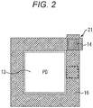
- Fig. 2 is a plan view illustrating a first configuration example (first embodiment) of a solid-state imaging element to which the present disclosure is applied. Note that the same reference numerals are given to constituent elements common to those of a conventional solid-state imaging element 10 illustrated in Fig. 1 , and therefore description thereof will be omitted appropriately.
- the FD 14 is formed at a position (indicated by a broken line in Fig. 2 ) below the light shielding wall 16 between adjacent pixels.
- an FD 14 is formed below a position (hereinafter also referred to as a cross portion 21) where light shielding walls 16 between pixels cross each other.
- the FD 14 is formed in a diagonal direction of a pixel, that is, below the cross portion 16 formed between adjacent pixels in an oblique direction.
- the position can be further separated from an optical center than the case where the FD 14 is formed below the light shielding wall 16. Therefore, generation of stray light can be further suppressed.
- the FD 14 may be disposed for each pixel, or a plurality of pixels may share the FD 14. However, in a case where a plurality of pixels shares the FD 14, in order to realize a global shutter, it is necessary to dispose a charge storage unit such as a memory other than the FD in each pixel.
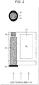
- Fig. 3 illustrates a cross-sectional view of the solid-state imaging element according to the first embodiment, illustrated in Fig. 2 .
- the FD 14 in the solid-state imaging element according to the first embodiment is formed below the cross portion 21 (as viewed from a light incident surface).
- the cross portion 21 is formed in, for example, a columnar shape.
- the cross portion 21 is not limited to a columnar shape, but may be an elliptical columnar shape or a polygonal pillar shape having a quadrangular pillar shape or more.
- the light shielding wall 16 and the cross portion 21 are formed by embedding a metal material in a hole opened by etching. Note that an antireflection film material such as an oxide film, an insulating film material, or the like may be embedded instead of the metal material.
- antireflection film material examples include hafnium oxide (HfO 2 ), aluminum oxide (Al 2 O 3 ), zirconium oxide (ZrO 2 ), tantalum oxide (Ta 2 O 5 ), titanium oxide (TiO 2 ), lanthanum oxide (La 2 O 3 ).
- Pr 2 O 3 praseodymium oxide
- CeO 2 cerium oxide
- Nd 2 O 3 neodymium oxide
- promethium oxide Pm 2 O 3
- Sm 2 O 3 samarium oxide
- Eu 2 O 3 europium oxide
- Gd 2 O 3 gadolinium oxide
- Tb 2 O 3 terbium oxide
- Dy 2 O 3 dysprosium oxide
- Ho 2 O 3 holmium oxide
- Ho 2 O 3 holmium oxide
- Tm 2 O 3 thulium oxide
- Yb 2 O 3 lutetium oxide
- Lu 2 O 3 yttrium oxide
- Y 2 O 3 silicon nitride
- the antireflection film material In a case where the antireflection film material is used, a difference in refractive index from the Si substrate 11 can cause total reflection of light. In addition, the thicknesses of the light shielding wall 16 and the cross portion 21 can be reduced, and therefore an effect of miniaturizing the solid-state imaging element can be expected.
- the insulating film examples include a Si compound (silicon oxide/silicon nitride/silicon oxynitride/silicon carbide, and the like).
- a light shielding cover 22 is formed with a metal material such as tungsten (W) above the cross portion 21 (light incident surface side).
- the light shielding cover 22 has such a size that the light shielding cover 22 covers the cross portion 21 and does not hinder incidence of light on the PD 13.
- the shape of the light shielding cover 22 may be any one of a circle, an ellipse, and a polygon having a quadrangular shape or more.
- Fig. 4 illustrates a process of manufacturing the solid-state imaging element according to the first embodiment.
- the Si substrate 11 on which the PD 13 and the FD 14 are formed is prepared. Subsequently, as illustrated in B of Fig. 4 , a pillar-shaped hole is dug in a position to form the light shielding wall 16 and the cross portion 21 by dry etching from the light incident surface side of the Si substrate 11.
- a metal material, an antireflection film material, or an insulating film material is filled into the dug hole.
- a metal material or the like above the PD 13 is scraped off.
- the light shielding cover 22 is formed above the cross portion 21.
- a color filter or an on-chip lens is placed on the light incident surface side of the Si substrate 11.
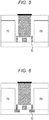
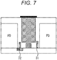
- Figs. 5 to 7 illustrate modified examples of the solid-state imaging element according to the first embodiment.
- Fig. 5 illustrates a modified example in which an element isolating portion 31 is added and formed by shallow trench isolation (STI).
- Fig. 6 illustrates a modified example in which a vertical transistor 32 is added and formed.
- Fig. 7 illustrates a modified example in which the element isolating portion 31 and the vertical transistor 32 are added and formed.
- STI shallow trench isolation
- Fig. 8 illustrates a cross-sectional view of a second configuration example (second embodiment) of the solid-state imaging element to which the present disclosure is applied.
- the solid-state imaging element according to the second embodiment is obtained by deforming the cross portion 21 according to the first embodiment, illustrated in Fig. 3 , from a column to a cylinder.
- the cross portion 21 may have a cylindrical shape of an ellipse or a polygon having a quadrangular shape or more.
- Fig. 9 illustrates a process of manufacturing the solid-state imaging element according to the second embodiment.
- the Si substrate 11 on which the PD 13 and the FD 14 are formed is prepared.
- a pillar-shaped groove is dug in a position to form a light shielding wall 16 and the cross portion 21 by dry etching from the light incident surface side of the Si substrate 11.
- a metal material, an antireflection film material, or an insulating film material is filled into the dug groove.
- a metal material or the like above the PD 13 is scraped off.
- a light shielding cover 22 is formed above the cross portion 21.
- a color filter or an on-chip lens is placed on the light incident surface side of the Si substrate 11.
- Figs. 10 to 14 illustrate modified examples of the solid-state imaging element according to the second embodiment.
- Fig. 10 illustrates a modified example in which an element isolating portion 31 is added and formed by STI outside the tubular cross portion 21.
- Fig. 11 illustrates a modified example in which a vertical transistor 32 is added and formed outside the tubular cross portion 21.
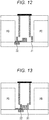
- Fig. 12 illustrates a modified example in which the element isolating portion 31 and the vertical transistor 32 are added and formed outside the tubular cross portion 21.
- Fig. 13 illustrates a modified example in which the element isolating portion 31 and the vertical transistor 32 are added and formed inside the tubular cross portion 21.
- Fig. 14 illustrates a modified example in which the vertical transistor 32 is added and formed inside the tubular cross portion 21, and the FD 14 is extended in a longitudinal direction inside the cross portion 21.
- the capacity thereof can be secured or increased without increasing the area thereof in a lateral direction.
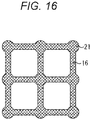
- the light shielding wall 16 between pixels and the cross portion 21 where the light shielding walls 16 cross each other are formed at the same time.
- the light shielding wall 16 and the cross portion 21 may be separately formed. In a case where the light shielding wall 16 and the cross portion 21 are separately formed, it is possible to separately set etching rates (depths) thereof.
- the light shielding wall 16 and the cross portion 21 may be integrally formed. In this case, it is necessary to set the etching rates (depths) of the light shielding wall 16 and the cross portion 21 to a common value.
- Fig. 17 is a cross-sectional view for one pixel of the solid-state imaging element according to the third embodiment.
- the light shielding cover 22 according to the first embodiment, illustrated in Fig. 3 is omitted.
- the light shielding cover 22 may be disposed.
- Fig. 18 is a plan view for six pixels of the solid-state imaging element according to the third embodiment. However, in Fig. 18 , illustration of a light shielding wall 16 and a cross portion 21 is omitted, and a region surrounded by a one-dot chain line is a constituent element for one pixel.
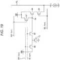
- Fig. 19 illustrates an equivalent circuit for one pixel of the solid-state imaging element according to the third embodiment.
- the solid-state imaging element according to the third embodiment has a configuration in which five transistors (MOS FETs) (TG 92, AMP 94, SEL 95, OFG 96, and RST 97) are used in addition to a PD 13 and a FD 14, and a source of the RST 97 and the FD 14 are integrally formed.
- MOS FETs five transistors
- a cross section of the solid-state imaging element according to the fourth embodiment is configured similarly to that of the third embodiment illustrated in Fig. 7 .
- the light shielding cover 22 according to the first embodiment, illustrated in Fig. 3 may be disposed or omitted.
- Fig. 20 is a plan view for six pixels of the solid-state imaging element according to the fourth embodiment. However, in Fig. 20 , illustration of a light shielding wall 16 and a cross portion 21 is omitted, and a region surrounded by a one-dot chain line is a constituent element for one pixel.
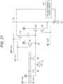
- Fig. 21 illustrates an equivalent circuit for one pixel of the solid-state imaging element according to the fourth embodiment.
- the fourth embodiment has a configuration in which a feedback enable (FBEN) transistor 111 and a voltage feedback control circuit 113 for controlling the FBEN transistor 111 are added to the third embodiment illustrated in Fig. 19 .
- FBEN feedback enable
- the solid-state imaging element according to the fourth embodiment has a configuration in which six transistors (MOS FETs) (TG 92, AMP 94, SEL 95, OFG 96, RST 97, and FBEN111) are used in addition to a PD 13 and a FD 14 and a source of the RST 97 and the FD 14 are integrally formed.
- MOS FETs six transistors
- kTc noise reset noise
- a cross section of the solid-state imaging element according to the fifth embodiment is configured similarly to that of the third embodiment illustrated in Fig. 7 .
- the light shielding cover 22 according to the first embodiment, illustrated in Fig. 3 may be disposed or omitted.
- Fig. 22 is a plan view for six pixels of the solid-state imaging element according to the fifth embodiment. However, in Fig. 22 , illustration of a light shielding wall 16 and a cross portion 21 is omitted, and a region surrounded by a one-dot chain line is a constituent element for one pixel.
- An equivalent circuit of the solid-state imaging element according to the fifth embodiment is the same as the equivalent circuit according to the third embodiment illustrated in Fig. 19 , and therefore illustration thereof is omitted.
- the solid-state imaging element according to the fifth embodiment has a configuration in which five transistors (MOS FETs) (TG 92, AMP 94, SEL 95, OFG 96, and RST 97) are used in addition to a PD 13 and a FD 14 similarly to the third embodiment, and a source of the RST 97 and the FD 14 are integrally formed.
- MOS FETs five transistors
- the AMP 94 and the SEL 95 are disposed adjacent to the RST 96, and a drain of the AMP 94 and a drain of the RST 97 share a single wire and are connected to the VDD 101. Therefore, the area occupied by the PD 13 in the area per pixel can be enlarged, and the light receiving sensitivity and the saturation charge amount can be increased.
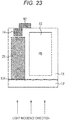
- Fig. 23 illustrates a modified example in which a moth eye structure unit 131 is added to a surface of the Si substrate 11.
- the moth eye structure unit 131 has been subjected to fine protrusion processing, and can reflect incident light irregularly. As a result, the incident light travels straight through the PD 13 not only in a thickness direction of the Si substrate 11 but also in a lateral direction and is reflected by the light shielding wall 16 or the cross portion 21. Therefore, an optical path length up to the FD 14 can be extended. Therefore, the amount of light that can reach the FD 14 can be suppressed (stray light can be suppressed).
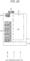
- Fig. 24 illustrates a modified example in which the thickness of the Si substrate 11 is increased and the length of the PD 13 in a thickness direction of the Si substrate 11 is increased accordingly.
- Fig. 25 illustrates a modified example in which a VG electrode 141 is added between the PD 13 and the TG 92.
- the VG electrode 141 By disposing the VG electrode 141, the optical path length up to the FD 14 can be extended, and therefore the amount of light that can reach the FD 14 can be suppressed. In addition, the VG electrode 141 can shield stray light with respect to the FD 14.
- modified examples illustrated in Figs. 23 to 25 can be appropriately combined with one another.
- modified examples can be applied not only to the third embodiment but also to other embodiments and modified examples thereof.
- the volume of the PD 13 is reduced by forming the light shielding wall 16 and the cross portion 21, leading to a decrease in the light receiving sensitivity and a decrease in the saturation charge amount.
- the absorption coefficient of light by the PD 13 depends on a wavelength, and is 8 ⁇ 10 4 [cm -1 ] for blue light (B) with a wavelength of 400 nm, 6 ⁇ 10 3 [cm -1 ] for green light (G) with a wavelength of 500 nm, and 2 ⁇ 10 3 [cm -1 ] for red light (R) with a wavelength of 700 nm. That is, among the R, G, and B light, the red light having a long wavelength has the poorest absorptivity in the PD 13, and the blue light having a short wavelength has the best absorptivity in the PD 13.
- the blue light is absorbed at a shallow position of the PD 13
- the green light is absorbed at a middle position of the PD 13
- the red light is absorbed at a deep position of the PD 13. Therefore, it can be said that a pixel receiving light with a longer wavelength has a higher risk of stray light with respect to the FD 14.
- the position, width, and depth of each of the light shielding wall 16 and the cross portion 21 are changed in accordance with the wavelength (that is, the color) of light to be received by a pixel.
- a light shielding cover 15 and a pillar-shaped light shielding wall 16 are formed between pixels, and an FD 14 is formed below the light shielding wall 16.
- the position of the light shielding wall 16 is formed so as to be enlarged toward the PD 13 side, and the volume of a PD 13 is reduced by the enlargement of the light shielding wall 16.
- an insulating film material having a lower refractive index than Si is embedded in the light shielding wall 16.
- an antireflection film material may be used instead of the insulating film material.
- a distance a between an end of the light shielding wall 16 and the center of the FD 14 below the light shielding wall 16 is longer than a distance b between an end of the light shielding wall 16 and the center of the FD 14 below light shielding wall 16 in a pixel of G (pixel receiving green light) adjacent to the pixel of R.
- the volume of the PD 13 at a shallow position and a middle position is reduced, but the volume of the PD 13 at a deep position mainly absorbing (photoelectrically converting) red light is not reduced. Therefore, an influence of volume reduction of the PD 13 can be suppressed.
- a distance between an end of the light shielding wall 16 and the center of the FD 14 below the light shielding wall 16 is shorter than that of the pixel of R.
- green light is mainly absorbed in the middle of the PD 13, and therefore it is considered that an influence of stray light passing through the pixel of G and reaching the FD 14 is small.
- the volume of the PD 13 can be larger in the pixel of G than that in the pixel of R.
- a pixel of B (pixel receiving blue light) is not illustrated but is assumed to be configured similarly to the pixel of G.
- Fig. 27 illustrates a modified example of the sixth embodiment.
- a metal material 151 is embedded in an insulating film material forming the pillar-shaped light shielding wall 16. Also in this modified example, a similar effect to that of the sixth embodiment can be obtained.
- a light shielding cover 15 and a tubular light shielding wall 16 are formed between pixels, and an FD 14 is formed below the light shielding wall 16.
- a material of the light shielding wall 16 is similar to that of the sixth embodiment. However, as for a pixel of R having the highest risk of stray light with respect to the FD 14, the position of the light shielding wall 16 is formed so as to be enlarged toward a PD 13 side, and the volume of the PD 13 is reduced by the enlargement of the light shielding wall 16.
- a lateral distance a between an end of the light shielding wall 16 and the center of the FD 14 below the light shielding wall 16 is longer than a lateral distance b between an end of the light shielding wall 16 and the center of the FD 14 below light shielding wall 16 in a pixel of G adjacent to the pixel of R.
- the volume of the PD 13 at a shallow position and a middle position is reduced, but the volume of the PD 13 at a deep position mainly absorbing (photoelectrically converting) red light is not reduced. Therefore, an influence of volume reduction of the PD 13 can be suppressed.
- a distance between an end of the light shielding wall 16 and the center of the FD 14 below the light shielding wall 16 is shorter than that of the pixel of R.
- green light is mainly absorbed in the middle of the PD 13, and therefore it is considered that an influence of stray light passing through the pixel of G and reaching the FD 14 is small.
- the volume of the PD 13 can be larger in the pixel of G than that in the pixel of R.
- a pixel of B is not illustrated but is assumed to be configured similarly to the pixel of G.
- a metal material may be embedded in the tubular light shielding wall 16. Also in this modified example, a similar effect to that of the seventh embodiment can be obtained.
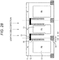
- each of a PD 13, a light shielding cover 15, and a light shielding wall 16 (including a cross portion 21) is formed in a common shape among pixels of the colors, and an FD 14 is formed below the light shielding wall 16.
- a material of the light shielding wall 16 is similar to that of the sixth embodiment.
- the FD 14 concerning a region of a pixel of R having the highest risk of stray light with respect to the FD 14 is formed at a position close to the side of a pixel of G adjacent to the pixel of R.
- a lateral distance a between an end of the light shielding wall 16 and the center of the FD 14 below the light shielding wall 16 is longer than a lateral distance b between an end of the light shielding wall 16 and the center of the FD 14 below light shielding wall 16 in a pixel of G adjacent to the pixel of R.
- a distance between an end of the light shielding wall 16 and the center of the FD 14 below the light shielding wall 16 is shorter than that of the pixel of R.
- green light is mainly absorbed in the middle of the PD 13, and therefore it is considered that an influence of stray light passing through the pixel of G and reaching the FD 14 is small.
- a pixel of B is not illustrated but is assumed to be configured similarly to the pixel of G.
- a metal material may be embedded in the pillar-shaped light shielding wall 16. Also in this modified example, a similar effect to that of the seventh embodiment can be obtained.
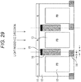
- a light shielding cover 15 and a tubular light shielding wall 16 are formed between pixels, and an FD 14 is formed below the light shielding wall 16.
- a material of the light shielding wall 16 is similar to that of the sixth embodiment. However, the depth of the light shielding wall 16 is different between the R pixel side where a risk of stray light with respect to an FD 14 is the highest and the G pixel side, and the light shielding wall 16 is formed more deeply on the R pixel side than that on the G pixel side.
- the shape of a PD 13 is different according to a difference in the depth of the light shielding wall 16 between the pixel of R and the pixel of G, and the shape of the PD 13 is reduced up to the depth where the light shielding wall 13 exists.
- the lateral distance a between an end of the light shielding wall 16 and the center of the FD 14 below the light shielding wall 16 is common, but the depth of the light shielding wall 16 is deeper in the pixel of R. Therefore, a similar effect to those of the above-described sixth to eighth embodiments can be achieved.
- Fig. 31 is a diagram illustrating a use example in which the solid-state imaging element according to any one of the above-described first to ninth embodiments is used.
- the above-described imaging element can be used in various cases of sensing light such as visible light, infrared light, ultraviolet light, or an X-ray.
- the technology according to the present disclosure (the present technology) can be applied to various products.
- Fig. 32 is a block diagram illustrating an example of a schematic configuration of a patient in-vivo information acquiring system using a capsule type endoscope to which the technology according to the present disclosure (the present technology) can be applied.
- An in-vivo information acquiring system 10001 includes a capsule type endoscope 10100 and an external control device 10200.
- the capsule type endoscope 10100 is swallowed by a patient at the time of examination.
- the capsule type endoscope 10100 has an imaging function and a wireless communication function. While moving inside an organ such as the stomach or the intestine by peristaltic movement or the like before natural discharge from a patient, the capsule type endoscope 10100 sequentially images an image of an inside of the organ (hereinafter also referred to as an in-vivo image) at predetermined intervals, and sequentially wirelessly transmits information regarding the in-vivo image to the external control device 10200 outside the body.
- an in-vivo image an image of an inside of the organ
- the external control device 10200 integrally controls an operation of the in-vivo information acquiring system 10001.
- the external control device 10200 receives information regarding the in-vivo image transmitted from the capsule type endoscope 10100, and generates image data for displaying the in-vivo image on a display device (not illustrated) on the basis of the received information regarding the in-vivo image.
- the in-vivo information acquiring system 10001 can obtain an in-vivo image obtained by imaging the state of an inside of a patient body at any time during a period between swallow of the capsule type endoscope 10100 and discharge thereof.
- the capsule type endoscope 10100 includes a capsule type casing 10101, and the casing 10101 houses a light source unit 10111, an imaging unit 10112, an image processing unit 10113, a wireless communication unit 10114, a power feed unit 10115, a power supply unit 10116, and a control unit 10117.
- the light source unit 10111 includes a light source such as a light emitting diode (LED), and irradiates an imaging field of view of the imaging unit 10112 with light, for example.
- a light source such as a light emitting diode (LED)
- LED light emitting diode
- the imaging unit 10112 includes an imaging element and an optical system including a plurality of lenses disposed in a preceding stage of the imaging element. Reflected light (hereinafter referred to as observation light) of light with which a body tissue as an observation target has been irradiated is collected by the optical system and is incident on the imaging element. In the imaging unit 10112, the imaging element photoelectrically converts observation light incident thereon, and an image signal corresponding to the observation light is generated. The image signal generated by the imaging unit 10112 is provided to the image processing unit 10113.
- observation light Reflected light (hereinafter referred to as observation light) of light with which a body tissue as an observation target has been irradiated is collected by the optical system and is incident on the imaging element.
- the imaging element photoelectrically converts observation light incident thereon, and an image signal corresponding to the observation light is generated.
- the image signal generated by the imaging unit 10112 is provided to the image processing unit 10113.
- the image processing unit 10113 includes a processor such as a central processing unit (CPU) or a graphics processing unit (GPU), and performs various signal processing on the image signal generated by the imaging unit 10112.
- the image processing unit 10113 provides the image signal subjected to the signal processing as RAW data to the wireless communication unit 10114.
- the wireless communication unit 10114 performs predetermined processing such as modulation processing on the image signal subjected to signal processing by the image processing unit 10113 and transmits the image signal to the external control device 10200 via an antenna 10114A.
- the wireless communication unit 10114 receives a control signal concerning driving control of the capsule type endoscope 10100 from the external control device 10200 via the antenna 10114A.
- the wireless communication unit 10114 provides the control signal received from the external control device 10200 to the control unit 10117.
- the power feed unit 10115 includes an antenna coil for power reception, a power regeneration circuit for regenerating power from a current generated in the antenna coil, a booster circuit, and the like.
- the power feed unit 10115 generates power using the principle of so-called non-contact charging.
- the power supply unit 10116 includes a secondary battery, and stores power generated by the power feed unit 10115.
- Fig. 32 in order to avoid complication of the drawing, illustration of an arrow or the like indicating the destination of power supply from the power supply unit 10116 is omitted.
- the power stored in the power supply unit 10116 is supplied to the light source unit 10111, the imaging unit 10112, the image processing unit 10113, the wireless communication unit 10114, and the control unit 10117, and can be used for driving of these units.
- the control unit 10117 includes a processor such as a CPU, and appropriately controls driving of the light source unit 10111, the imaging unit 10112, the image processing unit 10113, the wireless communication unit 10114, and the power feed unit 10115 according to a control signal transmitted from the external control device 10200.
- a processor such as a CPU
- the external control device 10200 includes a processor such as a CPU or a GPU, or a microcomputer, a control board, or the like on which a processor and a storage element such as a memory are mixedly mounted.
- the external control device 10200 controls an operation of the capsule type endoscope 10100 by transmitting a control signal to the control unit 10117 of the capsule type endoscope 10100 via an antenna 10200A.
- a control signal for example, light irradiation conditions with respect to an observation target in the light source unit 10111 can be changed by a control signal from the external control device 10200.
- imaging conditions for example, a frame rate in the imaging unit 10112, an exposure value, or the like
- imaging conditions can be changed by the control signal from the external control device 10200.
- the contents of the processing in the image processing unit 10113 and conditions under which the wireless communication unit 10114 transmits an image signal may be changed.
- the external control device 10200 performs various image processing on an image signal transmitted from the capsule type endoscope 10100, and generates image data for displaying the imaged in-vivo image on a display device.
- image processing for example, various signal processing such as development processing (demosaic processing), high image quality processing (band enhancement processing, super-resolution processing, noise reduction (NR) processing, and/or camera shake correction processing, for example), and/or enlargement processing (electronic zoom processing) can be performed.
- the external control device 10200 controls driving of the display device and causes the display device to display an in-vivo image imaged on the basis of the generated image data.
- the external control device 10200 may cause a recording device (not illustrated) to record the generated image data, or cause a printing device (not illustrated) to print out the generated image data.
- Fig. 33 is a diagram illustrating an example of a schematic configuration of an endoscopic surgical system to which the technology according to the present disclosure (the present technology) can be applied.
- Fig. 33 illustrates a situation in which a surgeon (physician) 11131 is performing surgery on a patient 11132 on a patient bed 11133 using an endoscopic surgical system 11000.
- the endoscopic surgical system 11000 includes an endoscope 11100, another surgical tool 11110 such as a pneumoperitoneum tube 11111 or an energy treatment tool 11112, a support arm device 11120 for supporting the endoscope 11100, and a cart 11200 on which various devices for endoscopic surgery are mounted.
- the endoscope 11100 includes a lens barrel 11101 to be inserted into a body cavity of the patient 11132 in a region of a predetermined length from a tip thereof, and a camera head 11102 connected to a proximal end of the lens barrel 11101.
- the endoscope 11100 configured as a so-called rigid mirror including the rigid lens barrel 11101 is illustrated, but the endoscope 11100 may be configured as a so-called flexible mirror including a flexible lens barrel.
- a light source device 11203 is connected to the endoscope 11100. Light generated by the light source device 11203 is guided to the tip of the lens barrel by a light guide extended inside the lens barrel 11101, and is emitted toward an observation target in a body cavity of the patient 11132 via the objective lens.
- the endoscope 11100 may be a direct view mirror, a perspective view mirror, or a side view mirror.
- An optical system and an imaging element are disposed inside the camera head 11102. Reflected light (observation light) from an observation target is converged on the imaging element by the optical system. The observation light is photoelectrically converted by the imaging element, and an electric signal corresponding to the observation light, that is, an image signal corresponding to an observation image is generated. The image signal is transmitted as RAW data to a camera control unit (CCU) 11201.
- CCU camera control unit
- the CCU 11201 includes a central processing unit (CPU), a graphics processing unit (GPU), and the like, and integrally controls operations of the endoscope 11100 and the display device 11202. Furthermore, the CCU 11201 receives an image signal from the camera head 11102, and performs, on the image signal, various image processing for displaying an image based on the image signal, such as development processing (demosaic processing), for example.
- CPU central processing unit
- GPU graphics processing unit
- the display device 11202 displays an image based on an image signal subjected to image processing by the CCU 11201 under the control of the CCU 11201.
- the light source device 11203 includes a light source such as a light emitting diode (LED), for example, and supplies irradiation light for imaging a surgical site or the like to the endoscope 11100.
- a light source such as a light emitting diode (LED), for example, and supplies irradiation light for imaging a surgical site or the like to the endoscope 11100.
- LED light emitting diode
- An input device 11204 is an input interface to the endoscopic surgical system 11000.
- a user can input various kinds of information and instructions to the endoscopic surgical system 11000 via the input device 11204.
- the user inputs an instruction or the like to change imaging conditions (type of irradiation light, magnification, focal length, and the like) by the endoscope 11100.
- a treatment tool control device 11205 controls driving of the energy treatment tool 11112 for cauterizing and cutting a tissue, sealing a blood vessel, or the like.
- a pneumoperitoneum device 11206 feeds a gas into a body cavity via the pneumoperitoneum tube 11111 in order to inflate the body cavity of the patient 11132 for the purpose of securing a field of view by the endoscope 11100 and securing a working space of a surgeon.
- a recorder 11207 is a device capable of recording various kinds of information regarding surgery.
- a printer 11208 is a device capable of printing various kinds of information regarding surgery in various formats such as a text, an image, and a graph.
- the light source device 11203 for supplying irradiation light used for imaging a surgical site to the endoscope 11100 may include an LED, a laser light source, or a white light source constituted by a combination thereof, for example.
- the white light source is constituted by a combination of RGB laser light sources, the output intensity and the output timing of each color (each wavelength) can be controlled with high precision, and therefore adjustment of a white balance of an imaged image can be performed by the light source device 11203.
- driving of the light source device 11203 may be controlled so as to change the intensity of light output at predetermined time intervals.
- driving of the imaging element of the camera head 11102 in synchronization with the timing of the change of the intensity of the light to acquire an image in a time division manner and synthesizing the image, a high dynamic range image without so-called blocked up shadows or blown out highlights can be generated.
- the light source device 11203 may be configured so as to be able to supply light in a predetermined wavelength band corresponding to special light observation.
- special light observation for example, by irradiation with light in a narrower band than irradiation light (that is, white light) at the time of ordinary observation using wavelength dependency of light absorption in a body tissue, a predetermined tissue such as a blood vessel of a mucosal surface layer is imaged at a high contrast, that is, so-called narrow band imaging is performed.
- fluorescence observation for obtaining an image by fluorescence generated by irradiation with excitation light may be performed.
- the fluorescence observation it is possible to observe fluorescence from a body tissue (autofluorescence observation) by irradiating the body tissue with excitation light, or to obtain a fluorescent image by injecting a reagent such as indocyanine green (ICG) into a body tissue and irradiating the body tissue with excitation light corresponding to a fluorescence wavelength of the reagent, for example.
- the light source device 11203 can be configured so as to be able to supply narrow band light and/or excitation light corresponding to such special light observation.
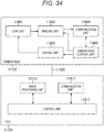
- Fig. 34 is a block diagram illustrating examples of functional configurations of the camera head 11102 and the CCU 11201 illustrated in Fig. 33 .
- the camera head 11102 includes a lens unit 11401, an imaging unit 11402, a driving unit 11403, a communication unit 11404, and a camera head control unit 11405.
- the CCU 11201 includes a communication unit 11411, an image processing unit 11412, and a control unit 11413.
- the camera head 11102 and the CCU 11201 are communicably connected to each other by a transmission cable 11400.
- the lens unit 11401 is an optical system disposed at a connecting portion with the lens barrel 11101. Observation light taken in from a tip of the lens barrel 11101 is guided to the camera head 11102 and is incident on the lens unit 11401.
- the lens unit 11401 includes a combination of a plurality of lenses including a zoom lens and a focus lens.
- the imaging unit 11402 includes an imaging element.
- the imaging unit 11402 may include one imaging element (so-called single plate type) or a plurality of imaging elements (so-called multiplate type).
- the imaging unit 11402 may include multiplate type imaging elements, for example, an image signal corresponding to each of RGB may be generated by each imaging element, and a color image may be obtained by synthesizing these image signals.
- the imaging unit 11402 may include a pair of imaging elements for acquiring an image signal for each of the right eye and the left eye corresponding to three-dimensional (3D) display. By performing the 3D display, the surgeon 11131 can grasp the depth of a living tissue in a surgical site more accurately.
- a plurality of lens units 11401 can be disposed corresponding to the respective imaging elements.
- the imaging unit 11402 is not necessarily disposed in the camera head 11102.
- the imaging unit 11402 may be disposed just behind an objective lens inside the lens barrel 11101.
- the driving unit 11403 includes an actuator, and moves a zoom lens and a focus lens of the lens unit 11401 by a predetermined distance along an optical axis under control of the camera head control unit 11405. As a result, the magnification and the focus of an image imaged by the imaging unit 11402 can be appropriately adjusted.
- the communication unit 11404 includes a communication device for transmitting and receiving various kinds of information to and from the CCU 11201.
- the communication unit 11404 transmits an image signal obtained from the imaging unit 11402 as RAW data to the CCU 11201 via the transmission cable 11400.
- the communication unit 11404 receives a control signal for controlling driving of the camera head 11102 from the CCU 11201, and supplies the control signal to the camera head control unit 11405.
- the control signal includes information regarding imaging conditions such as information indicating designation of a frame rate of an imaged image, information indicating designation of an exposure value at the time of imaging, and/or information indicating designation of the magnification and the focus of an imaged image, for example.
- the imaging conditions such as the frame rate, the exposure value, the magnification, and the focus may be appropriately designated by a user, or may be automatically set by the control unit 11413 of the CCU 11201 on the basis of an acquired image signal.
- the endoscope 11100 has a so-called auto exposure (AE) function, a so-called auto focus (AF) function, and a so-called auto white balance (AWB) function.
- AE auto exposure
- AF auto focus
- AVB auto white balance
- the camera head control unit 11405 controls driving of the camera head 11102 on the basis of a control signal from the CCU 11201 received via the communication unit 11404.
- the communication unit 11411 includes a communication device for transmitting and receiving various kinds of information to and from the camera head 11102.
- the communication unit 11411 receives an image signal transmitted from the camera head 11102 via the transmission cable 11400.
- the communication unit 11411 transmits a control signal for controlling driving of the camera head 11102 to the camera head 11102.
- the image signal and the control signal can be transmitted by electric communication, optical communication, or the like.
- the image processing unit 11412 performs various kinds of image processing on the image signal which is RAW data transmitted from the camera head 11102.
- the control unit 11413 performs various kinds of control concerning imaging of a surgical site or the like by the endoscope 11100 and display of an imaged image obtained by imaging a surgical site or the like. For example, the control unit 11413 generates a control signal for controlling driving of the camera head 11102.
- control unit 11413 causes the display device 11202 to display an imaged image of a surgical site or the like on the basis of an image signal subjected to image processing by the image processing unit 11412.
- control unit 11413 may recognize various objects in the imaged image using various image recognition techniques. For example, by detecting the shape, color, and the like of an edge of an object included in the imaged image, the control unit 11413 can recognize a surgical tool such as forceps, a specific living body part, bleeding, a mist at the time of using the energy treatment tool 11112, and the like.
- the control unit 11413 may cause the display device 11202 to superimpose and display various kinds of surgical support information on the image of the surgical site using the recognition result.
- the surgical support information is superimposed and displayed, and presented to the surgeon 11131. This makes it possible to reduce a burden on the surgeon 11131 and makes it possible for the surgeon 11131 to reliably perform surgery.
- the transmission cable 11400 connecting the camera head 11102 to the CCU 11201 is an electric signal cable corresponding to communication of an electric signal, an optical fiber corresponding to optical communication, or a composite cable thereof.
- communication is performed by wire using the transmission cable 11400, but communication between the camera head 11102 and the CCU 11201 may be performed wirelessly.
- endoscopic surgical system has been described as an example here.
- technology according to the present disclosure may also be applied to, for example, a microscopic surgery system or the like.
- the technology according to the present disclosure may be realized as a device mounted on any type of mobile body such as an automobile, an electric vehicle, a hybrid electric vehicle, a motorcycle, a bicycle, a personal mobility, an airplane, a drone, a ship, or a robot.
- Fig. 35 is a block diagram illustrating an example of a schematic configuration of a vehicle control system which is an example of a mobile body control system to which the technology according to the present disclosure can be applied.
- a vehicle control system 12000 includes a plurality of electronic control units connected to one another via a communication network 12001.
- the vehicle control system 12000 includes a drive system control unit 12010, a body system control unit 12020, a vehicle external information detection unit 12030, a vehicle internal information detection unit 12040, and an integrated control unit 12050.
- a microcomputer 12051, an audio image output unit 12052, and an on-vehicle network interface (I/F) 12053 are illustrated as a functional configuration of the integrated control unit 12050.
- the drive system control unit 12010 controls an operation of a device related to a drive system of a vehicle according to various programs.
- the drive system control unit 12010 functions as a control device of a driving force generating device for generating a driving force of a vehicle such as an internal combustion engine or a driving motor, a driving force transmitting mechanism for transmitting a driving force to wheels, a steering mechanism for adjusting a rudder angle of a vehicle, a braking device for generating a braking force of a vehicle, and the like.
- the body system control unit 12020 controls operations of various devices mounted on a vehicle body according to various programs.
- the body system control unit 12020 functions as a control device of a keyless entry system, a smart key system, a power window device, or various lamps such as a head lamp, a back lamp, a brake lamp, a turn indicator, and a fog lamp.
- a radio wave transmitted from a portable device substituted for a key or signals of various switches can be input.
- the body system control unit 12020 receives input of the radio wave or signals and controls a door lock device, a power window device, a lamp, and the like of a vehicle.
- the vehicle external information detection unit 12030 detects information outside a vehicle on which the vehicle control system 12000 is mounted. For example, to the vehicle external information detection unit 12030, an imaging unit 12031 is connected. The vehicle external information detection unit 12030 causes the imaging unit 12031 to image an image outside a vehicle and receives an imaged image. The vehicle external information detection unit 12030 may perform object detection processing or distance detection processing of a person, a car, an obstacle, a sign, a character on a road surface, or the like on the basis of the received image.
- the imaging unit 12031 is a light sensor for receiving light and outputting an electric signal corresponding to the amount of light received.
- the imaging unit 12031 can output an electric signal as an image or output the electric signal as distance measurement information.
- the light received by the imaging unit 12031 may be visible light or invisible light such as infrared light.
- the vehicle internal information detection unit 12040 detects information inside a vehicle.
- a driver state detection unit 12041 for detecting the state of a driver is connected to the vehicle internal information detection unit 12040.
- the driver state detection unit 12041 includes, for example, a camera for imaging a driver.
- the vehicle internal information detection unit 12040 may calculate the degree of fatigue or the degree of concentration of a driver or may determine whether the driver is dozing off on the basis of detection information input from the driver state detection unit 12041.
- the microcomputer 12051 can calculate a control target value of a driving force generating device, a steering mechanism, or a braking device on the basis of information inside and outside a vehicle, acquired by the vehicle external information detection unit 12030 or the vehicle internal information detection unit 12040, and can output a control command to the drive system control unit 12010.
- the microcomputer 12051 can perform cooperative control aiming at realizing a function of advanced driver assistance system (ADAS) including collision avoidance or impact mitigation of a vehicle, following travel based on inter-vehicle distance, vehicle speed maintenance travel, vehicle collision warning, vehicle lane departure warning, and the like.
- ADAS advanced driver assistance system
- the microcomputer 12051 can perform cooperative control aiming at, for example, automatic driving that autonomously travels without depending on driver's operation by controlling a driving force generating device, a steering mechanism, a braking device, or the like on the basis of information around a vehicle, acquired by the vehicle external information detection unit 12030 or the vehicle internal information detection unit 12040.
- the microcomputer 12051 can output a control command to the body system control unit 12020 on the basis of vehicle external information acquired by the vehicle external information detection unit 12030.
- the microcomputer 12051 can perform cooperative control aiming at antiglare such as switching from high beam to low beam by controlling a headlamp according to the position of a preceding vehicle or an oncoming vehicle detected by the vehicle external information detection unit 12030.
- the audio image output unit 12052 transmits an audio output signal and/or an image output signal to an output device capable of visually or audibly notifying a passenger of a vehicle or the outside of the vehicle of information.
- an audio speaker 12061 As the output device, an audio speaker 12061, a display unit 12062, and an instrument panel 12063 are illustrated.
- the display unit 12062 may include an on-board display and/or a head-up display, for example.
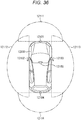
- Fig. 36 is a diagram illustrating an example of an installation position of the imaging unit 12031.
- the vehicle 12100 includes imaging units 12101, 12102, 12103, 12104, and 12105 as the imaging unit 12031.
- the imaging units 12101, 12102, 12103, 12104, and 12105 are disposed, for example, in a front nose, a side mirror, a rear bumper, and a back door of the vehicle 12100, in an upper portion of a front glass in a passenger compartment, and the like.
- the imaging unit 12101 disposed in a front nose and the imaging unit 12105 disposed in an upper portion of a front glass in a passenger compartment mainly acquire images in front of the vehicle 12100.
- the imaging units 12102 and 12103 disposed in side mirrors mainly acquire images on sides of the vehicle 12100.
- the imaging unit 12104 disposed in a rear bumper or a back door mainly acquires an image behind the vehicle 12100.
- the front images acquired by the imaging units 12101 and 12105 are mainly used for detecting a preceding vehicle, a pedestrian, an obstacle, a traffic signal, a traffic sign, a lane, or the like.
- FIG. 36 illustrates examples of imaging ranges of the imaging units 12101 to 12104.
- An imaging range 12111 indicates an imaging range of the imaging unit 12101 disposed in a front nose.
- Imaging ranges 12112 and 12113 indicate imaging ranges of the imaging units 12102 and 12103 disposed in side mirrors, respectively.
- An imaging range 12114 indicates an imaging range of the imaging unit 12104 disposed in a rear bumper or a back door. For example, by superimposing image data imaged by the imaging units 12101 to 12104 on one another, an overhead view image of the vehicle 12100 viewed from above is obtained.
- At least one of the imaging units 12101 to 12104 may have a function of acquiring distance information.
- at least one of the imaging units 12101 to 12104 may be a stereo camera including a plurality of imaging elements, or may be an imaging element having pixels for phase difference detection.
- the microcomputer 12051 determines a distance to each three-dimensional object in the imaging range 12111 to 12114 and a temporal change (relative speed with respect to the vehicle 12100) of the distance on the basis of the distance information obtained from the imaging units 12101 to 12104, and can thereby particularly extract a three-dimensional object which is the nearest three-dimensional object on a traveling path of the vehicle 12100 and is traveling at a predetermined speed (for example, 0 km/h or more) in substantially the same direction as the vehicle 12100 as a preceding vehicle.
- the microcomputer 12051 can set an inter-vehicle distance to be secured in advance in front of the preceding vehicle, and can perform automatic brake control (including following stop control), automatic acceleration control (including following start control), and the like. In this way, it is possible to perform cooperative control aiming at, for example, automatic driving that autonomously travels without depending on driver's operation.
- the microcomputer 12051 classifies three-dimensional object data related to a three-dimensional object into a two-wheeled vehicle, a regular vehicle, a large vehicle, a pedestrian, and another three-dimensional object such as a telegraph pole on the basis of the distance information obtained from the imaging units 12101 to 12104 and extracts data, and can use the extracted data for automatic avoidance of an obstacle.
- the microcomputer 12051 identifies an obstacle around the vehicle 12100 as an obstacle that a driver of the vehicle 12100 can see and an obstacle that is difficult to see. Then, the microcomputer 12051 judges a collision risk indicating a risk of collision with each obstacle.
- the microcomputer 12051 can perform driving assistance for avoiding collision by outputting an alarm to a driver via the audio speaker 12061 or the display unit 12062, or performing forced deceleration or avoiding steering via the drive system control unit 12010.
- At least one of the imaging units 12101 to 12104 may be an infrared camera for detecting an infrared ray.
- the microcomputer 12051 can recognize a pedestrian by determining whether or not a pedestrian exists in imaged images of the imaging units 12101 to 12104. Such recognition of a pedestrian is performed by, for example, a procedure of extracting characteristic points in imaged images of the imaging units 12101 to 12104 as infrared cameras and a procedure of performing pattern matching processing on a series of characteristic points indicating an outline of an object and determining whether or not a pedestrian exists.
- the audio image output unit 12052 controls the display unit 12062 such that the display unit 12062 superimposes and displays a rectangular contour line for emphasis on the recognized pedestrian.
- the audio image output unit 12052 may control the display unit 12062 such that the display unit 12062 displays an icon or the like indicating a pedestrian at a desired position.
- the present disclosure can have the following configurations.
Landscapes
- Engineering & Computer Science (AREA)
- Multimedia (AREA)
- Signal Processing (AREA)
- Solid State Image Pick-Up Elements (AREA)
- Transforming Light Signals Into Electric Signals (AREA)
Abstract
Description
- The present disclosure relates to a solid-state imaging element and an electronic device, and particularly to a solid-state imaging element suppressing stray light with respect to a floating diffusion (FD) or the like that temporarily holds a charge generated by a photoelectric conversion unit, and an electronic device.
- Conventionally, in a case where a global shutter is realized in a solid-state imaging element typified by a CMOS, a method for temporarily holding a charge photoelectrically converted by a photodiode (PD) or the like in a charge storage unit such as an FD and then reading out the charge is known.
- In addition, in order to suppress stray light with respect to an FD, a configuration is known in which the FD is disposed below a light shielding wall disposed between pixels (in a light incidence direction) (see, for example, Patent Document 1).
-
Fig. 1 is a cross-sectional view illustrating an example of a configuration of a conventional solid-state imaging element in which an FD is disposed below a light shielding wall. - In the solid-
state imaging element 10, alight shielding wall 16 in which a metal material or the like is embedded is formed between pixels of ani substrate 11. APD 13 is formed inside each pixel region of theSi substrate 11, and an FD 14 is formed below the light shielding wall 16 (in a light incidence direction). In addition, acolor filter 12 and an on-chip lens (not illustrated) are formed above theSi substrate 11. - In the solid-
state imaging element 10, light condensed by the on-chip lens and incident on thePD 13 via thecolor filter 12 is converted into a charge. The converted charge is accumulated in theFD 14 and then read out at a predetermined timing and converted into a pixel signal. - Patent Document 1: Japanese Patent Application Laid-Open No.
2014-96490 - In such a configuration as illustrated in
Fig. 1 , light shielding against theFD 14 may be insufficient, and the FD itself may perform photoelectric conversion in accordance with stray light, thereby generating a false signal. - The present disclosure has been achieved in view of such circumstances, and makes it possible to further suppress stray light with respect to a charge storage unit such as an FD than related art.
- A solid-state imaging element according to a first aspect of the present disclosure is constituted by many pixels and includes: a photoelectric conversion unit formed for each of the pixels and configured to convert incident light into a charge; a charge storage unit configured to temporarily hold the converted charge; and a first light shielding unit formed between the pixels and having a predetermined length in a thickness direction of a substrate, in which the charge storage unit is formed below a cross portion where the first light shielding unit formed between pixels adjacent to each other in a longitudinal direction crosses the first light shielding unit formed between pixels adjacent to each other in a lateral direction.
- The solid-state imaging element according to the first aspect of the present disclosure may further include a second light shielding unit covering a light incident surface side of the cross portion.
- The cross portion may be formed in a columnar shape or a polygonal pillar shape.
- The cross portion may be formed in a cylindrical shape or a polygonal tubular shape.
- The charge storage unit may be extended in a thickness direction of a substrate in a tube of the cross portion formed in a tubular shape.
- The first light shielding unit and the cross portion may be formed individually at different etching rates.
- The solid-state imaging element according to the first aspect of the present disclosure may further include a TG transistor, an AMP transistor, a SEL transistor, an OFG transistor, and an RST transistor, and the charge storage unit and a source of the RST transistor may be integrally formed.
- The solid-state imaging element according to the first aspect of the present disclosure may further include an FBEN transistor for suppressing reset noise.
- A drain of the AMP transistor and a drain of the RST transistor may share a wire and be connected to VDD.
- The solid-state imaging element according to the first aspect of the present disclosure may further include a moth eye structure unit for irregularly reflecting incident light to the photoelectric conversion unit.
- In the first light shielding unit, lengths in a planar direction of a substrate in adjacent pixel regions may be different from each other.
- In the first light shielding unit, lengths in a thickness direction of a substrate in adjacent pixel regions may be different from each other.
- The photoelectric conversion unit of one pixel may have a different volume from the photoelectric conversion unit of a pixel adjacent thereto.
- The pixel may include at least a first pixel sensitive to light having a first wavelength, a second pixel sensitive to a second wavelength longer than the first wavelength, and a third pixel sensitive to a third wavelength longer than the second wavelength.
- In the first light shielding unit formed between the first or second pixel and the third pixel, the length in a planar direction of a substrate in a region of the third pixel may be longer than that in a region of the first or second pixel.
- In the first light shielding unit formed between the first or second pixel and the third pixel, the length in a thickness direction of a substrate in a region of the third pixel may be longer than that in a region of the first or second pixel.
- The photoelectric conversion unit of the third pixel may have a smaller volume than the photoelectric conversion unit of the first or second pixel.
- The charge storage unit formed between the first or second pixel and the third pixel may be formed at a position close to the first or second pixel side.
- The charge storage unit may be shared by a plurality of pixels.
- An electronic device according to a second aspect of the present disclosure has a solid-state imaging element constituted by many pixels mounted thereon, in which the solid-state imaging element includes: a photoelectric conversion unit formed for each of the pixels and configured to convert incident light into a charge; a charge storage unit configured to temporarily hold the converted charge; and a first light shielding unit formed between the pixels and having a predetermined length in a thickness direction of a substrate, and the charge storage unit is formed below a cross portion where the first light shielding unit formed between pixels adjacent to each other in a longitudinal direction crosses the first light shielding unit formed between pixels adjacent to each other in a lateral direction.
- According to the first and second aspects of the present disclosure, it is possible to suppress stray light with respect to the photoelectric conversion unit and to reduce generation of a false signal.
-
-
Fig. 1 is a cross-sectional view illustrating a configuration example of a conventional solid-state imaging element. -
Fig. 2 is a plan view illustrating a first configuration example of a solid-state imaging element to which the present disclosure is applied. -
Fig. 3 is a cross-sectional view illustrating the first configuration example of the solid-state imaging element to which the present disclosure is applied. -
Fig. 4 is a view for explaining a manufacturing process of the first configuration example of the solid-state imaging element. -
Fig. 5 is a plan view illustrating a modified example of the first configuration example of the solid-state imaging element. -
Fig. 6 is a plan view illustrating a modified example of the first configuration example of the solid-state imaging element. -
Fig. 7 is a plan view illustrating a modified example of the first configuration example of the solid-state imaging element. -
Fig. 8 is a cross-sectional view illustrating a second configuration example of the solid-state imaging element to which the present disclosure is applied. -
Fig. 9 is a view for explaining a manufacturing process of the second configuration example of the solid-state imaging element. -
Fig. 10 is a plan view illustrating a modified example of the second configuration example of the solid-state imaging element. -
Fig. 11 is a plan view illustrating a modified example of the second configuration example of the solid-state imaging element. -
Fig. 12 is a plan view illustrating a modified example of the second configuration example of the solid-state imaging element. -
Fig. 13 is a plan view illustrating a modified example of the second configuration example of the solid-state imaging element. -
Fig. 14 is a plan view illustrating a modified example of the second configuration example of the solid-state imaging element. -
Fig. 15 is a plan view in a case where a light shielding wall and a cross portion are separately formed. -
Fig. 16 is a plan view in a case where a light shielding wall and a cross portion are integrally formed. -
Fig. 17 is a cross-sectional view illustrating a third configuration example of the solid-state imaging element to which the present disclosure is applied. -
Fig. 18 is a plan view illustrating the third configuration example of the solid-state imaging element to which the present disclosure is applied. -
Fig. 19 is an equivalent circuit diagram of the third configuration example of the solid-state imaging element. -
Fig. 20 is a plan view illustrating a fourth configuration example of the solid-state imaging element to which the present disclosure is applied. -
Fig. 21 is an equivalent circuit diagram of the fourth configuration example of the solid-state imaging element. -
Fig. 22 is a plan view illustrating a fifth configuration example of the solid-state imaging element to which the present disclosure is applied. -
Fig. 23 is a cross-sectional view illustrating a modified example of the third configuration example of the solid-state imaging element. -
Fig. 24 is a cross-sectional view illustrating a modified example of the third configuration example of the solid-state imaging element. -
Fig. 25 is a cross-sectional view illustrating a modified example of the third configuration example of the solid-state imaging element. -
Fig. 26 is a cross-sectional view illustrating a sixth configuration example of the solid-state imaging element to which the present disclosure is applied. -
Fig. 27 is a cross-sectional view illustrating a modified example of the sixth configuration example of the solid-state imaging element. -
Fig. 28 is a cross-sectional view illustrating a seventh configuration example of the solid-state imaging element to which the present disclosure is applied. -
Fig. 29 is a cross-sectional view illustrating an eighth configuration example of the solid-state imaging element to which the present disclosure is applied. -
Fig. 30 is a cross-sectional view illustrating a ninth configuration example of the solid-state imaging element to which the present disclosure is applied. -
Fig. 31 is a diagram illustrating a use example of a solid-state imaging element. -
Fig. 32 is a block diagram illustrating an example of a schematic configuration of an in-vivo information acquiring system. -
Fig. 33 is a diagram illustrating an example of a schematic configuration of an endoscopic surgical system. -
Fig. 34 is a block diagram illustrating examples of functional configurations of a camera head and a CCU. -
Fig. 35 is a block diagram illustrating an example of a schematic configuration of a vehicle control system. -
Fig. 36 is an explanatory diagram illustrating examples of installation positions of a vehicle external information detection unit and an imaging unit. - Hereinafter, best modes (hereinafter referred to as embodiments) for carrying out the present disclosure will be described in detail with reference to the drawings.
-
Fig. 2 is a plan view illustrating a first configuration example (first embodiment) of a solid-state imaging element to which the present disclosure is applied. Note that the same reference numerals are given to constituent elements common to those of a conventional solid-state imaging element 10 illustrated inFig. 1 , and therefore description thereof will be omitted appropriately. - In the solid-
state imaging element 10, theFD 14 is formed at a position (indicated by a broken line inFig. 2 ) below thelight shielding wall 16 between adjacent pixels. Meanwhile, in a solid-state imaging element according to a first embodiment, anFD 14 is formed below a position (hereinafter also referred to as a cross portion 21) wherelight shielding walls 16 between pixels cross each other. In other words, theFD 14 is formed in a diagonal direction of a pixel, that is, below thecross portion 16 formed between adjacent pixels in an oblique direction. - By forming the
FD 14 below the cross portion, the position can be further separated from an optical center than the case where theFD 14 is formed below thelight shielding wall 16. Therefore, generation of stray light can be further suppressed. - Note that the
FD 14 may be disposed for each pixel, or a plurality of pixels may share theFD 14. However, in a case where a plurality of pixels shares theFD 14, in order to realize a global shutter, it is necessary to dispose a charge storage unit such as a memory other than the FD in each pixel. -
Fig. 3 illustrates a cross-sectional view of the solid-state imaging element according to the first embodiment, illustrated inFig. 2 . As described above, theFD 14 in the solid-state imaging element according to the first embodiment is formed below the cross portion 21 (as viewed from a light incident surface). - The
cross portion 21 is formed in, for example, a columnar shape. However, thecross portion 21 is not limited to a columnar shape, but may be an elliptical columnar shape or a polygonal pillar shape having a quadrangular pillar shape or more. - The
light shielding wall 16 and thecross portion 21 are formed by embedding a metal material in a hole opened by etching. Note that an antireflection film material such as an oxide film, an insulating film material, or the like may be embedded instead of the metal material. - Examples of the antireflection film material include hafnium oxide (HfO2), aluminum oxide (Al2O3), zirconium oxide (ZrO2), tantalum oxide (Ta2O5), titanium oxide (TiO2), lanthanum oxide (La2O3). praseodymium oxide (Pr2O3), cerium oxide (CeO2), neodymium oxide (Nd2O3), promethium oxide (Pm2O3), samarium oxide (Sm2O3), europium oxide (Eu2O3), gadolinium oxide ((Gd2O3), terbium oxide (Tb2O3), dysprosium oxide (Dy2O3), holmium oxide (Ho2O3), thulium oxide (Tm2O3), ytterbium oxide (Yb2O3), lutetium oxide (Lu2O3), yttrium oxide (Y2O3), and silicon nitride (SiN).
- In a case where the antireflection film material is used, a difference in refractive index from the
Si substrate 11 can cause total reflection of light. In addition, the thicknesses of thelight shielding wall 16 and thecross portion 21 can be reduced, and therefore an effect of miniaturizing the solid-state imaging element can be expected. - Examples of the insulating film include a Si compound (silicon oxide/silicon nitride/silicon oxynitride/silicon carbide, and the like).
- A
light shielding cover 22 is formed with a metal material such as tungsten (W) above the cross portion 21 (light incident surface side). Thelight shielding cover 22 has such a size that thelight shielding cover 22 covers thecross portion 21 and does not hinder incidence of light on thePD 13. The shape of thelight shielding cover 22 may be any one of a circle, an ellipse, and a polygon having a quadrangular shape or more. - Next,
Fig. 4 illustrates a process of manufacturing the solid-state imaging element according to the first embodiment. - First, as illustrated in A of
Fig. 4 , theSi substrate 11 on which thePD 13 and theFD 14 are formed is prepared. Subsequently, as illustrated in B ofFig. 4 , a pillar-shaped hole is dug in a position to form thelight shielding wall 16 and thecross portion 21 by dry etching from the light incident surface side of theSi substrate 11. - Subsequently, as illustrated in C of
Fig. 4 , a metal material, an antireflection film material, or an insulating film material is filled into the dug hole. Thereafter, as illustrated in D ofFig. 4 , a metal material or the like above thePD 13 is scraped off. Finally, as illustrated in E ofFig. 4 , thelight shielding cover 22 is formed above thecross portion 21. Thereafter, a color filter or an on-chip lens is placed on the light incident surface side of theSi substrate 11. -
Figs. 5 to 7 illustrate modified examples of the solid-state imaging element according to the first embodiment. -
Fig. 5 illustrates a modified example in which anelement isolating portion 31 is added and formed by shallow trench isolation (STI).Fig. 6 illustrates a modified example in which avertical transistor 32 is added and formed.Fig. 7 illustrates a modified example in which theelement isolating portion 31 and thevertical transistor 32 are added and formed. - Next,
Fig. 8 illustrates a cross-sectional view of a second configuration example (second embodiment) of the solid-state imaging element to which the present disclosure is applied. - The solid-state imaging element according to the second embodiment is obtained by deforming the
cross portion 21 according to the first embodiment, illustrated inFig. 3 , from a column to a cylinder. Note that thecross portion 21 may have a cylindrical shape of an ellipse or a polygon having a quadrangular shape or more. -
Fig. 9 illustrates a process of manufacturing the solid-state imaging element according to the second embodiment. - First, as illustrated in A of
Fig. 4 , theSi substrate 11 on which thePD 13 and theFD 14 are formed is prepared. Subsequently, as illustrated in B ofFig. 9 , a pillar-shaped groove is dug in a position to form alight shielding wall 16 and thecross portion 21 by dry etching from the light incident surface side of theSi substrate 11. - Subsequently, as illustrated in C of
Fig. 9 , a metal material, an antireflection film material, or an insulating film material is filled into the dug groove. Thereafter, as illustrated in D ofFig. 9 , a metal material or the like above thePD 13 is scraped off. Finally, as illustrated in E ofFig. 9 , alight shielding cover 22 is formed above thecross portion 21. Thereafter, a color filter or an on-chip lens is placed on the light incident surface side of theSi substrate 11. -
Figs. 10 to 14 illustrate modified examples of the solid-state imaging element according to the second embodiment. -
Fig. 10 illustrates a modified example in which anelement isolating portion 31 is added and formed by STI outside thetubular cross portion 21.Fig. 11 illustrates a modified example in which avertical transistor 32 is added and formed outside thetubular cross portion 21.Fig. 12 illustrates a modified example in which theelement isolating portion 31 and thevertical transistor 32 are added and formed outside thetubular cross portion 21.Fig. 13 illustrates a modified example in which theelement isolating portion 31 and thevertical transistor 32 are added and formed inside thetubular cross portion 21. -
Fig. 14 illustrates a modified example in which thevertical transistor 32 is added and formed inside thetubular cross portion 21, and theFD 14 is extended in a longitudinal direction inside thecross portion 21. By extending theFD 14 in the longitudinal direction, the capacity thereof can be secured or increased without increasing the area thereof in a lateral direction. - Note that in the above description, the
light shielding wall 16 between pixels and thecross portion 21 where thelight shielding walls 16 cross each other are formed at the same time. However, as illustrated inFig. 15 , thelight shielding wall 16 and thecross portion 21 may be separately formed. In a case where thelight shielding wall 16 and thecross portion 21 are separately formed, it is possible to separately set etching rates (depths) thereof. - Of course, as illustrated in
Fig. 16 , thelight shielding wall 16 and thecross portion 21 may be integrally formed. In this case, it is necessary to set the etching rates (depths) of thelight shielding wall 16 and thecross portion 21 to a common value. - Next, a third configuration example (third embodiment) of the solid-state imaging element to which the present disclosure is applied will be described with reference to
Figs. 17 to 19 . -
Fig. 17 is a cross-sectional view for one pixel of the solid-state imaging element according to the third embodiment. As is apparent fromFig. 17 , in the third embodiment, thelight shielding cover 22 according to the first embodiment, illustrated inFig. 3 , is omitted. However, thelight shielding cover 22 may be disposed. -
Fig. 18 is a plan view for six pixels of the solid-state imaging element according to the third embodiment. However, inFig. 18 , illustration of alight shielding wall 16 and across portion 21 is omitted, and a region surrounded by a one-dot chain line is a constituent element for one pixel. -
Fig. 19 illustrates an equivalent circuit for one pixel of the solid-state imaging element according to the third embodiment. As illustrated inFig. 19 , the solid-state imaging element according to the third embodiment has a configuration in which five transistors (MOS FETs) (TG 92,AMP 94,SEL 95,OFG 96, and RST 97) are used in addition to aPD 13 and aFD 14, and a source of theRST 97 and theFD 14 are integrally formed. - In the solid-state imaging element according to the third embodiment, by making the source of the
RST 97 and theFD 14 common, false signal generation points are consolidated into one place, and the source of theRST 97 and theFD 14 are disposed below thecross portion 21. Therefore, generation of a false signal due to stray light can be suppressed. - Next, a fourth configuration example (fourth embodiment) of the solid-state imaging element to which the present disclosure is applied will be described with reference to
Figs. 20 and21 . - A cross section of the solid-state imaging element according to the fourth embodiment is configured similarly to that of the third embodiment illustrated in
Fig. 7 . Also in the fourth embodiment, thelight shielding cover 22 according to the first embodiment, illustrated inFig. 3 , may be disposed or omitted. -
Fig. 20 is a plan view for six pixels of the solid-state imaging element according to the fourth embodiment. However, inFig. 20 , illustration of alight shielding wall 16 and across portion 21 is omitted, and a region surrounded by a one-dot chain line is a constituent element for one pixel. -
Fig. 21 illustrates an equivalent circuit for one pixel of the solid-state imaging element according to the fourth embodiment. As illustrated inFig. 21 , the fourth embodiment has a configuration in which a feedback enable (FBEN)transistor 111 and a voltagefeedback control circuit 113 for controlling theFBEN transistor 111 are added to the third embodiment illustrated inFig. 19 . - That is, the solid-state imaging element according to the fourth embodiment has a configuration in which six transistors (MOS FETs) (
TG 92,AMP 94,SEL 95,OFG 96,RST 97, and FBEN111) are used in addition to aPD 13 and aFD 14 and a source of theRST 97 and theFD 14 are integrally formed. - In the solid-state imaging element according to the fourth embodiment, by making the source of the
RST 97 and theFD 14 common, false signal generation points are consolidated into one place, and the source of theRST 97 and theFD 14 are disposed below thecross portion 21, and therefore generation of a false signal due to stray light can be suppressed. - In addition, in the solid-state imaging element according to the fourth embodiment, by disposing the
FBEN 111 and the voltagefeedback control circuit 113, kTc noise (reset noise) can be suppressed. - Next, a fifth configuration example (fifth embodiment) of the solid-state imaging element to which the present disclosure is applied will be described with reference to
Fig. 22 . - A cross section of the solid-state imaging element according to the fifth embodiment is configured similarly to that of the third embodiment illustrated in
Fig. 7 . Also in the fifth embodiment, thelight shielding cover 22 according to the first embodiment, illustrated inFig. 3 , may be disposed or omitted. -
Fig. 22 is a plan view for six pixels of the solid-state imaging element according to the fifth embodiment. However, inFig. 22 , illustration of alight shielding wall 16 and across portion 21 is omitted, and a region surrounded by a one-dot chain line is a constituent element for one pixel. - An equivalent circuit of the solid-state imaging element according to the fifth embodiment is the same as the equivalent circuit according to the third embodiment illustrated in
Fig. 19 , and therefore illustration thereof is omitted. - As illustrated in
Fig. 22 , the solid-state imaging element according to the fifth embodiment has a configuration in which five transistors (MOS FETs) (TG 92,AMP 94,SEL 95,OFG 96, and RST 97) are used in addition to aPD 13 and aFD 14 similarly to the third embodiment, and a source of theRST 97 and theFD 14 are integrally formed. - In the solid-state imaging element according to the fifth embodiment, by making the source of the
RST 97 and theFD 14 common, false signal generation points are consolidated into one place, and the source of theRST 97 and theFD 14 are disposed below thecross portion 21, and therefore generation of a false signal due to stray light can be suppressed. - Furthermore, in the solid-state imaging element according to the fifth embodiment, the
AMP 94 and theSEL 95 are disposed adjacent to theRST 96, and a drain of theAMP 94 and a drain of theRST 97 share a single wire and are connected to the VDD 101. Therefore, the area occupied by thePD 13 in the area per pixel can be enlarged, and the light receiving sensitivity and the saturation charge amount can be increased. - Next, a modified example of the solid-state imaging element according to the third embodiment, illustrated in
Fig. 17 , will be described with reference toFigs. 23 to 25 . -
Fig. 23 illustrates a modified example in which a motheye structure unit 131 is added to a surface of theSi substrate 11. - The moth
eye structure unit 131 has been subjected to fine protrusion processing, and can reflect incident light irregularly. As a result, the incident light travels straight through thePD 13 not only in a thickness direction of theSi substrate 11 but also in a lateral direction and is reflected by thelight shielding wall 16 or thecross portion 21. Therefore, an optical path length up to theFD 14 can be extended. Therefore, the amount of light that can reach theFD 14 can be suppressed (stray light can be suppressed). -
Fig. 24 illustrates a modified example in which the thickness of theSi substrate 11 is increased and the length of thePD 13 in a thickness direction of theSi substrate 11 is increased accordingly. - By increasing the length of the
PD 13, it is possible to increase the light receiving sensitivity and the saturation charge amount of thePD 13, and also to extend the optical path length up to theFD 14. Therefore, the amount of light that can reach theFD 14 can be suppressed (stray light can be suppressed). -
Fig. 25 illustrates a modified example in which aVG electrode 141 is added between thePD 13 and theTG 92. - By disposing the
VG electrode 141, the optical path length up to theFD 14 can be extended, and therefore the amount of light that can reach theFD 14 can be suppressed. In addition, theVG electrode 141 can shield stray light with respect to theFD 14. - Note that the modified examples illustrated in
Figs. 23 to 25 can be appropriately combined with one another. In addition, the modified examples can be applied not only to the third embodiment but also to other embodiments and modified examples thereof. - In the first to fifth embodiments described above, by forming the
FD 14 below thecross portion 21, an effect of suppressing stray light with respect to theFD 14 is achieved. However, there is also a disadvantage of disposing thecross portion 21 and thelight shielding wall 16. - For example, in a case where the volume per pixel in the Si substrate is determined, the volume of the
PD 13 is reduced by forming thelight shielding wall 16 and thecross portion 21, leading to a decrease in the light receiving sensitivity and a decrease in the saturation charge amount. - Hereinafter, a configuration example in which an influence of volume reduction of the
PD 13 can be minimized while thelight shielding wall 16 and thecross portion 21 are disposed will be described. Before the description, characteristics of thePD 13 will be described. - The absorption coefficient of light by the
PD 13 depends on a wavelength, and is 8 × 10⁴ [cm-1] for blue light (B) with a wavelength of 400 nm, 6 × 10³ [cm-1] for green light (G) with a wavelength of 500 nm, and 2 × 10³ [cm-1] for red light (R) with a wavelength of 700 nm. That is, among the R, G, and B light, the red light having a long wavelength has the poorest absorptivity in thePD 13, and the blue light having a short wavelength has the best absorptivity in thePD 13. - In other words, the blue light is absorbed at a shallow position of the
PD 13, the green light is absorbed at a middle position of thePD 13, and the red light is absorbed at a deep position of thePD 13. Therefore, it can be said that a pixel receiving light with a longer wavelength has a higher risk of stray light with respect to theFD 14. - Therefore, in the embodiments described below, in order to minimize an influence of volume reduction of the
PD 13, the position, width, and depth of each of thelight shielding wall 16 and thecross portion 21 are changed in accordance with the wavelength (that is, the color) of light to be received by a pixel. - Next, a sixth configuration example (sixth embodiment) of the solid-state imaging element to which the present disclosure is applied will be described with reference to
Fig. 26 . - In the solid-state imaging element according to the sixth embodiment, similarly to the first embodiment illustrated in
Fig. 3 , alight shielding cover 15 and a pillar-shaped light shielding wall 16 (including a cross portion 21) are formed between pixels, and anFD 14 is formed below thelight shielding wall 16. However, as for a pixel of R (a pixel receiving red light) having the highest risk of stray light with respect to theFD 14, the position of thelight shielding wall 16 is formed so as to be enlarged toward thePD 13 side, and the volume of aPD 13 is reduced by the enlargement of thelight shielding wall 16. - Note that, in the case of the sixth embodiment, an insulating film material having a lower refractive index than Si is embedded in the
light shielding wall 16. However, an antireflection film material may be used instead of the insulating film material. - That is, in a case where attention is paid to the pixel of R in the sixth embodiment, a distance a between an end of the
light shielding wall 16 and the center of theFD 14 below thelight shielding wall 16 is longer than a distance b between an end of thelight shielding wall 16 and the center of theFD 14 belowlight shielding wall 16 in a pixel of G (pixel receiving green light) adjacent to the pixel of R. This makes it possible to suppress stray light passing through the pixel of R and reaching theFD 14. In addition, the volume of thePD 13 at a shallow position and a middle position is reduced, but the volume of thePD 13 at a deep position mainly absorbing (photoelectrically converting) red light is not reduced. Therefore, an influence of volume reduction of thePD 13 can be suppressed. - Meanwhile, in a case where attention is paid to the pixel of G, a distance between an end of the
light shielding wall 16 and the center of theFD 14 below thelight shielding wall 16 is shorter than that of the pixel of R. However, green light is mainly absorbed in the middle of thePD 13, and therefore it is considered that an influence of stray light passing through the pixel of G and reaching theFD 14 is small. In addition, the volume of thePD 13 can be larger in the pixel of G than that in the pixel of R. - Note that a pixel of B (pixel receiving blue light) is not illustrated but is assumed to be configured similarly to the pixel of G.
-
Fig. 27 illustrates a modified example of the sixth embodiment. In this modified example, ametal material 151 is embedded in an insulating film material forming the pillar-shapedlight shielding wall 16. Also in this modified example, a similar effect to that of the sixth embodiment can be obtained. - Next, a seventh configuration example (seventh embodiment) of the solid-state imaging element to which the present disclosure is applied will be described with reference to
Fig. 28 . - In the solid-state imaging element according to the seventh embodiment, similarly to the second embodiment illustrated in
Fig. 8 , alight shielding cover 15 and a tubular light shielding wall 16 (including a cross portion 21) are formed between pixels, and anFD 14 is formed below thelight shielding wall 16. A material of thelight shielding wall 16 is similar to that of the sixth embodiment. However, as for a pixel of R having the highest risk of stray light with respect to theFD 14, the position of thelight shielding wall 16 is formed so as to be enlarged toward aPD 13 side, and the volume of thePD 13 is reduced by the enlargement of thelight shielding wall 16. - That is, in a case where attention is paid to the pixel of R in the seventh embodiment, a lateral distance a between an end of the
light shielding wall 16 and the center of theFD 14 below thelight shielding wall 16 is longer than a lateral distance b between an end of thelight shielding wall 16 and the center of theFD 14 belowlight shielding wall 16 in a pixel of G adjacent to the pixel of R. This makes it possible to suppress stray light passing through the pixel of R and reaching theFD 14. In addition, the volume of thePD 13 at a shallow position and a middle position is reduced, but the volume of thePD 13 at a deep position mainly absorbing (photoelectrically converting) red light is not reduced. Therefore, an influence of volume reduction of thePD 13 can be suppressed. - Meanwhile, in a case where attention is paid to the pixel of G, a distance between an end of the
light shielding wall 16 and the center of theFD 14 below thelight shielding wall 16 is shorter than that of the pixel of R. However, green light is mainly absorbed in the middle of thePD 13, and therefore it is considered that an influence of stray light passing through the pixel of G and reaching theFD 14 is small. In addition, the volume of thePD 13 can be larger in the pixel of G than that in the pixel of R. - Note that a pixel of B is not illustrated but is assumed to be configured similarly to the pixel of G.
- As a modified example of the seventh embodiment, a metal material may be embedded in the tubular
light shielding wall 16. Also in this modified example, a similar effect to that of the seventh embodiment can be obtained. - Next, an eighth configuration example (eighth embodiment) of the solid-state imaging element to which the present disclosure is applied will be described with reference to
Fig. 29 . - In the solid-state imaging element according to the eighth embodiment, each of a
PD 13, alight shielding cover 15, and a light shielding wall 16 (including a cross portion 21) is formed in a common shape among pixels of the colors, and anFD 14 is formed below thelight shielding wall 16. A material of thelight shielding wall 16 is similar to that of the sixth embodiment. - However, the
FD 14 concerning a region of a pixel of R having the highest risk of stray light with respect to theFD 14 is formed at a position close to the side of a pixel of G adjacent to the pixel of R. - That is, in a case where attention is paid to the pixel of R in the eighth embodiment, a lateral distance a between an end of the
light shielding wall 16 and the center of theFD 14 below thelight shielding wall 16 is longer than a lateral distance b between an end of thelight shielding wall 16 and the center of theFD 14 belowlight shielding wall 16 in a pixel of G adjacent to the pixel of R. This makes it possible to suppress stray light passing through the pixel of R and reaching theFD 14. Meanwhile, in a case where attention is paid to the pixel of G, a distance between an end of thelight shielding wall 16 and the center of theFD 14 below thelight shielding wall 16 is shorter than that of the pixel of R. However, green light is mainly absorbed in the middle of thePD 13, and therefore it is considered that an influence of stray light passing through the pixel of G and reaching theFD 14 is small. - Note that a pixel of B is not illustrated but is assumed to be configured similarly to the pixel of G.
- As a modified example of the eighth embodiment, a metal material may be embedded in the pillar-shaped
light shielding wall 16. Also in this modified example, a similar effect to that of the seventh embodiment can be obtained. - Next, a ninth configuration example (ninth embodiment) of the solid-state imaging element to which the present disclosure is applied will be described with reference to
Fig. 30 . - In the solid-state imaging element according to the ninth embodiment, similarly to the second embodiment illustrated in
Fig. 8 , alight shielding cover 15 and a tubular light shielding wall 16 (including a cross portion 21) are formed between pixels, and anFD 14 is formed below thelight shielding wall 16. A material of thelight shielding wall 16 is similar to that of the sixth embodiment. However, the depth of thelight shielding wall 16 is different between the R pixel side where a risk of stray light with respect to anFD 14 is the highest and the G pixel side, and thelight shielding wall 16 is formed more deeply on the R pixel side than that on the G pixel side. In addition, the shape of aPD 13 is different according to a difference in the depth of thelight shielding wall 16 between the pixel of R and the pixel of G, and the shape of thePD 13 is reduced up to the depth where thelight shielding wall 13 exists. - That is, in the pixel of R and the pixel of G in the ninth embodiment, the lateral distance a between an end of the
light shielding wall 16 and the center of theFD 14 below thelight shielding wall 16 is common, but the depth of thelight shielding wall 16 is deeper in the pixel of R. Therefore, a similar effect to those of the above-described sixth to eighth embodiments can be achieved. - The above-described first to ninth embodiments and modified examples thereof can be appropriately combined with one another.
-
Fig. 31 is a diagram illustrating a use example in which the solid-state imaging element according to any one of the above-described first to ninth embodiments is used. - As described below, for example, the above-described imaging element can be used in various cases of sensing light such as visible light, infrared light, ultraviolet light, or an X-ray.
-
- An apparatus for imaging an image used for appreciation, such as a digital camera or a portable device with a camera function
- An apparatus used for transportation, such as a vehicle-mounted sensor for imaging the front, the back, the surrounding, the inside, or the like of an automobile for safe driving such as automatic stop, for recognition of a driver's condition, and the like, a surveillance camera for monitoring a running vehicle and a road, or a measuring sensor for measuring a distance between vehicles or the like
- An apparatus used for home electronics, such as a television set, a refrigerator, or an air conditioner for imaging a gesture of a user and operating a device according to the gesture
- An apparatus used for medical care and health care, such as an endoscope or an apparatus for receiving infrared light for angiography
- An apparatus used for security, such as a surveillance camera for crime prevention or a camera for personal authentication
- An apparatus used for beauty care, such as a skin measurement device for imaging a skin or a microscope for imaging a scalp
- An apparatus used for sports, such as an action camera or a wearable camera for sports and the like
- An apparatus used for agriculture, such as a camera for monitoring a condition of a field and a crop
- The technology according to the present disclosure (the present technology) can be applied to various products.
-
Fig. 32 is a block diagram illustrating an example of a schematic configuration of a patient in-vivo information acquiring system using a capsule type endoscope to which the technology according to the present disclosure (the present technology) can be applied. - An in-vivo
information acquiring system 10001 includes acapsule type endoscope 10100 and anexternal control device 10200. - The
capsule type endoscope 10100 is swallowed by a patient at the time of examination. Thecapsule type endoscope 10100 has an imaging function and a wireless communication function. While moving inside an organ such as the stomach or the intestine by peristaltic movement or the like before natural discharge from a patient, thecapsule type endoscope 10100 sequentially images an image of an inside of the organ (hereinafter also referred to as an in-vivo image) at predetermined intervals, and sequentially wirelessly transmits information regarding the in-vivo image to theexternal control device 10200 outside the body. - The
external control device 10200 integrally controls an operation of the in-vivoinformation acquiring system 10001. In addition, theexternal control device 10200 receives information regarding the in-vivo image transmitted from thecapsule type endoscope 10100, and generates image data for displaying the in-vivo image on a display device (not illustrated) on the basis of the received information regarding the in-vivo image. - In this way, the in-vivo
information acquiring system 10001 can obtain an in-vivo image obtained by imaging the state of an inside of a patient body at any time during a period between swallow of thecapsule type endoscope 10100 and discharge thereof. - The configurations and functions of the
capsule type endoscope 10100 and theexternal control device 10200 will be described in more detail. - The
capsule type endoscope 10100 includes acapsule type casing 10101, and thecasing 10101 houses alight source unit 10111, animaging unit 10112, animage processing unit 10113, awireless communication unit 10114, apower feed unit 10115, apower supply unit 10116, and acontrol unit 10117. - The
light source unit 10111 includes a light source such as a light emitting diode (LED), and irradiates an imaging field of view of theimaging unit 10112 with light, for example. - The
imaging unit 10112 includes an imaging element and an optical system including a plurality of lenses disposed in a preceding stage of the imaging element. Reflected light (hereinafter referred to as observation light) of light with which a body tissue as an observation target has been irradiated is collected by the optical system and is incident on the imaging element. In theimaging unit 10112, the imaging element photoelectrically converts observation light incident thereon, and an image signal corresponding to the observation light is generated. The image signal generated by theimaging unit 10112 is provided to theimage processing unit 10113. - The
image processing unit 10113 includes a processor such as a central processing unit (CPU) or a graphics processing unit (GPU), and performs various signal processing on the image signal generated by theimaging unit 10112. Theimage processing unit 10113 provides the image signal subjected to the signal processing as RAW data to thewireless communication unit 10114. - The
wireless communication unit 10114 performs predetermined processing such as modulation processing on the image signal subjected to signal processing by theimage processing unit 10113 and transmits the image signal to theexternal control device 10200 via anantenna 10114A. In addition, thewireless communication unit 10114 receives a control signal concerning driving control of thecapsule type endoscope 10100 from theexternal control device 10200 via theantenna 10114A. Thewireless communication unit 10114 provides the control signal received from theexternal control device 10200 to thecontrol unit 10117. - The
power feed unit 10115 includes an antenna coil for power reception, a power regeneration circuit for regenerating power from a current generated in the antenna coil, a booster circuit, and the like. Thepower feed unit 10115 generates power using the principle of so-called non-contact charging. - The
power supply unit 10116 includes a secondary battery, and stores power generated by thepower feed unit 10115. InFig. 32 , in order to avoid complication of the drawing, illustration of an arrow or the like indicating the destination of power supply from thepower supply unit 10116 is omitted. However, the power stored in thepower supply unit 10116 is supplied to thelight source unit 10111, theimaging unit 10112, theimage processing unit 10113, thewireless communication unit 10114, and thecontrol unit 10117, and can be used for driving of these units. - The
control unit 10117 includes a processor such as a CPU, and appropriately controls driving of thelight source unit 10111, theimaging unit 10112, theimage processing unit 10113, thewireless communication unit 10114, and thepower feed unit 10115 according to a control signal transmitted from theexternal control device 10200. - The
external control device 10200 includes a processor such as a CPU or a GPU, or a microcomputer, a control board, or the like on which a processor and a storage element such as a memory are mixedly mounted. Theexternal control device 10200 controls an operation of thecapsule type endoscope 10100 by transmitting a control signal to thecontrol unit 10117 of thecapsule type endoscope 10100 via anantenna 10200A. In thecapsule type endoscope 10100, for example, light irradiation conditions with respect to an observation target in thelight source unit 10111 can be changed by a control signal from theexternal control device 10200. In addition, imaging conditions (for example, a frame rate in theimaging unit 10112, an exposure value, or the like) can be changed by the control signal from theexternal control device 10200. In addition, depending on the control signal from theexternal control device 10200, the contents of the processing in theimage processing unit 10113 and conditions under which thewireless communication unit 10114 transmits an image signal (for example, a transmission interval, the number of transmitted images, or the like) may be changed. - In addition, the
external control device 10200 performs various image processing on an image signal transmitted from thecapsule type endoscope 10100, and generates image data for displaying the imaged in-vivo image on a display device. As the image processing, for example, various signal processing such as development processing (demosaic processing), high image quality processing (band enhancement processing, super-resolution processing, noise reduction (NR) processing, and/or camera shake correction processing, for example), and/or enlargement processing (electronic zoom processing) can be performed. Theexternal control device 10200 controls driving of the display device and causes the display device to display an in-vivo image imaged on the basis of the generated image data. Alternatively, theexternal control device 10200 may cause a recording device (not illustrated) to record the generated image data, or cause a printing device (not illustrated) to print out the generated image data. - An example of the in-vivo information acquiring system to which the technology according to the present disclosure can be applied has been described above.
-
Fig. 33 is a diagram illustrating an example of a schematic configuration of an endoscopic surgical system to which the technology according to the present disclosure (the present technology) can be applied. -
Fig. 33 illustrates a situation in which a surgeon (physician) 11131 is performing surgery on apatient 11132 on apatient bed 11133 using an endoscopicsurgical system 11000. As illustrated in the drawing, the endoscopicsurgical system 11000 includes anendoscope 11100, anothersurgical tool 11110 such as apneumoperitoneum tube 11111 or anenergy treatment tool 11112, asupport arm device 11120 for supporting theendoscope 11100, and acart 11200 on which various devices for endoscopic surgery are mounted. - The
endoscope 11100 includes alens barrel 11101 to be inserted into a body cavity of thepatient 11132 in a region of a predetermined length from a tip thereof, and acamera head 11102 connected to a proximal end of thelens barrel 11101. In the illustrated example, theendoscope 11100 configured as a so-called rigid mirror including therigid lens barrel 11101 is illustrated, but theendoscope 11100 may be configured as a so-called flexible mirror including a flexible lens barrel. - At the tip of the
lens barrel 11101, an opening into which an objective lens is fitted is disposed. Alight source device 11203 is connected to theendoscope 11100. Light generated by thelight source device 11203 is guided to the tip of the lens barrel by a light guide extended inside thelens barrel 11101, and is emitted toward an observation target in a body cavity of thepatient 11132 via the objective lens. Note that theendoscope 11100 may be a direct view mirror, a perspective view mirror, or a side view mirror. - An optical system and an imaging element are disposed inside the
camera head 11102. Reflected light (observation light) from an observation target is converged on the imaging element by the optical system. The observation light is photoelectrically converted by the imaging element, and an electric signal corresponding to the observation light, that is, an image signal corresponding to an observation image is generated. The image signal is transmitted as RAW data to a camera control unit (CCU) 11201. - The
CCU 11201 includes a central processing unit (CPU), a graphics processing unit (GPU), and the like, and integrally controls operations of theendoscope 11100 and thedisplay device 11202. Furthermore, theCCU 11201 receives an image signal from thecamera head 11102, and performs, on the image signal, various image processing for displaying an image based on the image signal, such as development processing (demosaic processing), for example. - The
display device 11202 displays an image based on an image signal subjected to image processing by theCCU 11201 under the control of theCCU 11201. - The
light source device 11203 includes a light source such as a light emitting diode (LED), for example, and supplies irradiation light for imaging a surgical site or the like to theendoscope 11100. - An
input device 11204 is an input interface to the endoscopicsurgical system 11000. A user can input various kinds of information and instructions to the endoscopicsurgical system 11000 via theinput device 11204. For example, the user inputs an instruction or the like to change imaging conditions (type of irradiation light, magnification, focal length, and the like) by theendoscope 11100. - A treatment
tool control device 11205 controls driving of theenergy treatment tool 11112 for cauterizing and cutting a tissue, sealing a blood vessel, or the like. Apneumoperitoneum device 11206 feeds a gas into a body cavity via thepneumoperitoneum tube 11111 in order to inflate the body cavity of thepatient 11132 for the purpose of securing a field of view by theendoscope 11100 and securing a working space of a surgeon. Arecorder 11207 is a device capable of recording various kinds of information regarding surgery. Aprinter 11208 is a device capable of printing various kinds of information regarding surgery in various formats such as a text, an image, and a graph. - Note that the
light source device 11203 for supplying irradiation light used for imaging a surgical site to theendoscope 11100 may include an LED, a laser light source, or a white light source constituted by a combination thereof, for example. In a case where the white light source is constituted by a combination of RGB laser light sources, the output intensity and the output timing of each color (each wavelength) can be controlled with high precision, and therefore adjustment of a white balance of an imaged image can be performed by thelight source device 11203. In addition, in this case, by irradiating an observation target with laser light from each of the RGB laser light sources in a time division manner and controlling driving of an imaging element of thecamera head 11102 in synchronization with the irradiation timing, it is also possible to image an image corresponding to each of RGB in a time division manner. According to this method, a color image can be obtained without disposing a color filter in the imaging element. - In addition, driving of the
light source device 11203 may be controlled so as to change the intensity of light output at predetermined time intervals. By controlling driving of the imaging element of thecamera head 11102 in synchronization with the timing of the change of the intensity of the light to acquire an image in a time division manner and synthesizing the image, a high dynamic range image without so-called blocked up shadows or blown out highlights can be generated. - In addition, the
light source device 11203 may be configured so as to be able to supply light in a predetermined wavelength band corresponding to special light observation. In the special light observation, for example, by irradiation with light in a narrower band than irradiation light (that is, white light) at the time of ordinary observation using wavelength dependency of light absorption in a body tissue, a predetermined tissue such as a blood vessel of a mucosal surface layer is imaged at a high contrast, that is, so-called narrow band imaging is performed. Alternatively, in the special light observation, fluorescence observation for obtaining an image by fluorescence generated by irradiation with excitation light may be performed. In the fluorescence observation, it is possible to observe fluorescence from a body tissue (autofluorescence observation) by irradiating the body tissue with excitation light, or to obtain a fluorescent image by injecting a reagent such as indocyanine green (ICG) into a body tissue and irradiating the body tissue with excitation light corresponding to a fluorescence wavelength of the reagent, for example. Thelight source device 11203 can be configured so as to be able to supply narrow band light and/or excitation light corresponding to such special light observation. -
Fig. 34 is a block diagram illustrating examples of functional configurations of thecamera head 11102 and theCCU 11201 illustrated inFig. 33 . - The
camera head 11102 includes alens unit 11401, animaging unit 11402, adriving unit 11403, acommunication unit 11404, and a camerahead control unit 11405. TheCCU 11201 includes acommunication unit 11411, animage processing unit 11412, and acontrol unit 11413. Thecamera head 11102 and theCCU 11201 are communicably connected to each other by atransmission cable 11400. - The
lens unit 11401 is an optical system disposed at a connecting portion with thelens barrel 11101. Observation light taken in from a tip of thelens barrel 11101 is guided to thecamera head 11102 and is incident on thelens unit 11401. Thelens unit 11401 includes a combination of a plurality of lenses including a zoom lens and a focus lens. - The
imaging unit 11402 includes an imaging element. Theimaging unit 11402 may include one imaging element (so-called single plate type) or a plurality of imaging elements (so-called multiplate type). In a case where theimaging unit 11402 includes multiplate type imaging elements, for example, an image signal corresponding to each of RGB may be generated by each imaging element, and a color image may be obtained by synthesizing these image signals. Alternatively, theimaging unit 11402 may include a pair of imaging elements for acquiring an image signal for each of the right eye and the left eye corresponding to three-dimensional (3D) display. By performing the 3D display, thesurgeon 11131 can grasp the depth of a living tissue in a surgical site more accurately. Incidentally, in a case where theimaging unit 11402 includes multiplate type imaging elements, a plurality oflens units 11401 can be disposed corresponding to the respective imaging elements. - In addition, the
imaging unit 11402 is not necessarily disposed in thecamera head 11102. For example, theimaging unit 11402 may be disposed just behind an objective lens inside thelens barrel 11101. - The driving
unit 11403 includes an actuator, and moves a zoom lens and a focus lens of thelens unit 11401 by a predetermined distance along an optical axis under control of the camerahead control unit 11405. As a result, the magnification and the focus of an image imaged by theimaging unit 11402 can be appropriately adjusted. - The
communication unit 11404 includes a communication device for transmitting and receiving various kinds of information to and from theCCU 11201. Thecommunication unit 11404 transmits an image signal obtained from theimaging unit 11402 as RAW data to theCCU 11201 via thetransmission cable 11400. - In addition, the
communication unit 11404 receives a control signal for controlling driving of thecamera head 11102 from theCCU 11201, and supplies the control signal to the camerahead control unit 11405. The control signal includes information regarding imaging conditions such as information indicating designation of a frame rate of an imaged image, information indicating designation of an exposure value at the time of imaging, and/or information indicating designation of the magnification and the focus of an imaged image, for example. - Note that the imaging conditions such as the frame rate, the exposure value, the magnification, and the focus may be appropriately designated by a user, or may be automatically set by the
control unit 11413 of theCCU 11201 on the basis of an acquired image signal. In the latter case, theendoscope 11100 has a so-called auto exposure (AE) function, a so-called auto focus (AF) function, and a so-called auto white balance (AWB) function. - The camera
head control unit 11405 controls driving of thecamera head 11102 on the basis of a control signal from theCCU 11201 received via thecommunication unit 11404. - The
communication unit 11411 includes a communication device for transmitting and receiving various kinds of information to and from thecamera head 11102. Thecommunication unit 11411 receives an image signal transmitted from thecamera head 11102 via thetransmission cable 11400. - In addition, the
communication unit 11411 transmits a control signal for controlling driving of thecamera head 11102 to thecamera head 11102. The image signal and the control signal can be transmitted by electric communication, optical communication, or the like. - The
image processing unit 11412 performs various kinds of image processing on the image signal which is RAW data transmitted from thecamera head 11102. - The
control unit 11413 performs various kinds of control concerning imaging of a surgical site or the like by theendoscope 11100 and display of an imaged image obtained by imaging a surgical site or the like. For example, thecontrol unit 11413 generates a control signal for controlling driving of thecamera head 11102. - In addition, the
control unit 11413 causes thedisplay device 11202 to display an imaged image of a surgical site or the like on the basis of an image signal subjected to image processing by theimage processing unit 11412. In this case, thecontrol unit 11413 may recognize various objects in the imaged image using various image recognition techniques. For example, by detecting the shape, color, and the like of an edge of an object included in the imaged image, thecontrol unit 11413 can recognize a surgical tool such as forceps, a specific living body part, bleeding, a mist at the time of using theenergy treatment tool 11112, and the like. When thedisplay device 11202 displays the imaged image, thecontrol unit 11413 may cause thedisplay device 11202 to superimpose and display various kinds of surgical support information on the image of the surgical site using the recognition result. The surgical support information is superimposed and displayed, and presented to thesurgeon 11131. This makes it possible to reduce a burden on thesurgeon 11131 and makes it possible for thesurgeon 11131 to reliably perform surgery. - The
transmission cable 11400 connecting thecamera head 11102 to theCCU 11201 is an electric signal cable corresponding to communication of an electric signal, an optical fiber corresponding to optical communication, or a composite cable thereof. - Here, in the illustrated example, communication is performed by wire using the
transmission cable 11400, but communication between thecamera head 11102 and theCCU 11201 may be performed wirelessly. - An example of the endoscopic surgical system to which the technology according to the present disclosure can be applied has been described above.
- Note that the endoscopic surgical system has been described as an example here. However, the technology according to the present disclosure may also be applied to, for example, a microscopic surgery system or the like.
- For example, the technology according to the present disclosure (the present technology) may be realized as a device mounted on any type of mobile body such as an automobile, an electric vehicle, a hybrid electric vehicle, a motorcycle, a bicycle, a personal mobility, an airplane, a drone, a ship, or a robot.
-
Fig. 35 is a block diagram illustrating an example of a schematic configuration of a vehicle control system which is an example of a mobile body control system to which the technology according to the present disclosure can be applied. - A
vehicle control system 12000 includes a plurality of electronic control units connected to one another via acommunication network 12001. In the example illustrated inFig. 35 , thevehicle control system 12000 includes a drivesystem control unit 12010, a bodysystem control unit 12020, a vehicle externalinformation detection unit 12030, a vehicle internalinformation detection unit 12040, and anintegrated control unit 12050. In addition, as a functional configuration of theintegrated control unit 12050, amicrocomputer 12051, an audioimage output unit 12052, and an on-vehicle network interface (I/F) 12053 are illustrated. - The drive
system control unit 12010 controls an operation of a device related to a drive system of a vehicle according to various programs. For example, the drivesystem control unit 12010 functions as a control device of a driving force generating device for generating a driving force of a vehicle such as an internal combustion engine or a driving motor, a driving force transmitting mechanism for transmitting a driving force to wheels, a steering mechanism for adjusting a rudder angle of a vehicle, a braking device for generating a braking force of a vehicle, and the like. - The body
system control unit 12020 controls operations of various devices mounted on a vehicle body according to various programs. For example, the bodysystem control unit 12020 functions as a control device of a keyless entry system, a smart key system, a power window device, or various lamps such as a head lamp, a back lamp, a brake lamp, a turn indicator, and a fog lamp. In this case, to the bodysystem control unit 12020, a radio wave transmitted from a portable device substituted for a key or signals of various switches can be input. The bodysystem control unit 12020 receives input of the radio wave or signals and controls a door lock device, a power window device, a lamp, and the like of a vehicle. - The vehicle external
information detection unit 12030 detects information outside a vehicle on which thevehicle control system 12000 is mounted. For example, to the vehicle externalinformation detection unit 12030, animaging unit 12031 is connected. The vehicle externalinformation detection unit 12030 causes theimaging unit 12031 to image an image outside a vehicle and receives an imaged image. The vehicle externalinformation detection unit 12030 may perform object detection processing or distance detection processing of a person, a car, an obstacle, a sign, a character on a road surface, or the like on the basis of the received image. - The
imaging unit 12031 is a light sensor for receiving light and outputting an electric signal corresponding to the amount of light received. Theimaging unit 12031 can output an electric signal as an image or output the electric signal as distance measurement information. In addition, the light received by theimaging unit 12031 may be visible light or invisible light such as infrared light. - The vehicle internal
information detection unit 12040 detects information inside a vehicle. To the vehicle internalinformation detection unit 12040, for example, a driverstate detection unit 12041 for detecting the state of a driver is connected. The driverstate detection unit 12041 includes, for example, a camera for imaging a driver. The vehicle internalinformation detection unit 12040 may calculate the degree of fatigue or the degree of concentration of a driver or may determine whether the driver is dozing off on the basis of detection information input from the driverstate detection unit 12041. - The
microcomputer 12051 can calculate a control target value of a driving force generating device, a steering mechanism, or a braking device on the basis of information inside and outside a vehicle, acquired by the vehicle externalinformation detection unit 12030 or the vehicle internalinformation detection unit 12040, and can output a control command to the drivesystem control unit 12010. For example, themicrocomputer 12051 can perform cooperative control aiming at realizing a function of advanced driver assistance system (ADAS) including collision avoidance or impact mitigation of a vehicle, following travel based on inter-vehicle distance, vehicle speed maintenance travel, vehicle collision warning, vehicle lane departure warning, and the like. - In addition, the
microcomputer 12051 can perform cooperative control aiming at, for example, automatic driving that autonomously travels without depending on driver's operation by controlling a driving force generating device, a steering mechanism, a braking device, or the like on the basis of information around a vehicle, acquired by the vehicle externalinformation detection unit 12030 or the vehicle internalinformation detection unit 12040. - In addition, the
microcomputer 12051 can output a control command to the bodysystem control unit 12020 on the basis of vehicle external information acquired by the vehicle externalinformation detection unit 12030. For example, themicrocomputer 12051 can perform cooperative control aiming at antiglare such as switching from high beam to low beam by controlling a headlamp according to the position of a preceding vehicle or an oncoming vehicle detected by the vehicle externalinformation detection unit 12030. - The audio
image output unit 12052 transmits an audio output signal and/or an image output signal to an output device capable of visually or audibly notifying a passenger of a vehicle or the outside of the vehicle of information. In the example ofFig. 35 , as the output device, anaudio speaker 12061, adisplay unit 12062, and an instrument panel 12063 are illustrated. Thedisplay unit 12062 may include an on-board display and/or a head-up display, for example. -
Fig. 36 is a diagram illustrating an example of an installation position of theimaging unit 12031. - In
Fig. 36 , thevehicle 12100 includesimaging units imaging unit 12031. - The
imaging units vehicle 12100, in an upper portion of a front glass in a passenger compartment, and the like. Theimaging unit 12101 disposed in a front nose and theimaging unit 12105 disposed in an upper portion of a front glass in a passenger compartment mainly acquire images in front of thevehicle 12100. Theimaging units vehicle 12100. Theimaging unit 12104 disposed in a rear bumper or a back door mainly acquires an image behind thevehicle 12100. The front images acquired by theimaging units - Note that
Fig. 36 illustrates examples of imaging ranges of theimaging units 12101 to 12104. Animaging range 12111 indicates an imaging range of theimaging unit 12101 disposed in a front nose. Imaging ranges 12112 and 12113 indicate imaging ranges of theimaging units imaging range 12114 indicates an imaging range of theimaging unit 12104 disposed in a rear bumper or a back door. For example, by superimposing image data imaged by theimaging units 12101 to 12104 on one another, an overhead view image of thevehicle 12100 viewed from above is obtained. - At least one of the
imaging units 12101 to 12104 may have a function of acquiring distance information. For example, at least one of theimaging units 12101 to 12104 may be a stereo camera including a plurality of imaging elements, or may be an imaging element having pixels for phase difference detection. - For example, the
microcomputer 12051 determines a distance to each three-dimensional object in theimaging range 12111 to 12114 and a temporal change (relative speed with respect to the vehicle 12100) of the distance on the basis of the distance information obtained from theimaging units 12101 to 12104, and can thereby particularly extract a three-dimensional object which is the nearest three-dimensional object on a traveling path of thevehicle 12100 and is traveling at a predetermined speed (for example, 0 km/h or more) in substantially the same direction as thevehicle 12100 as a preceding vehicle. Furthermore, themicrocomputer 12051 can set an inter-vehicle distance to be secured in advance in front of the preceding vehicle, and can perform automatic brake control (including following stop control), automatic acceleration control (including following start control), and the like. In this way, it is possible to perform cooperative control aiming at, for example, automatic driving that autonomously travels without depending on driver's operation. - For example, the
microcomputer 12051 classifies three-dimensional object data related to a three-dimensional object into a two-wheeled vehicle, a regular vehicle, a large vehicle, a pedestrian, and another three-dimensional object such as a telegraph pole on the basis of the distance information obtained from theimaging units 12101 to 12104 and extracts data, and can use the extracted data for automatic avoidance of an obstacle. For example, themicrocomputer 12051 identifies an obstacle around thevehicle 12100 as an obstacle that a driver of thevehicle 12100 can see and an obstacle that is difficult to see. Then, themicrocomputer 12051 judges a collision risk indicating a risk of collision with each obstacle. When the collision risk is higher than a set value and there is a possibility of collision, themicrocomputer 12051 can perform driving assistance for avoiding collision by outputting an alarm to a driver via theaudio speaker 12061 or thedisplay unit 12062, or performing forced deceleration or avoiding steering via the drivesystem control unit 12010. - At least one of the
imaging units 12101 to 12104 may be an infrared camera for detecting an infrared ray. For example, themicrocomputer 12051 can recognize a pedestrian by determining whether or not a pedestrian exists in imaged images of theimaging units 12101 to 12104. Such recognition of a pedestrian is performed by, for example, a procedure of extracting characteristic points in imaged images of theimaging units 12101 to 12104 as infrared cameras and a procedure of performing pattern matching processing on a series of characteristic points indicating an outline of an object and determining whether or not a pedestrian exists. If themicrocomputer 12051 determines that a pedestrian exists in imaged images of theimaging units 12101 to 12104 and recognizes a pedestrian, the audioimage output unit 12052 controls thedisplay unit 12062 such that thedisplay unit 12062 superimposes and displays a rectangular contour line for emphasis on the recognized pedestrian. In addition, the audioimage output unit 12052 may control thedisplay unit 12062 such that thedisplay unit 12062 displays an icon or the like indicating a pedestrian at a desired position. - An example of the vehicle control system to which the technology according to the present disclosure can be applied has been described above.
- Note that the embodiments of the present disclosure are not limited to the above-described embodiments, and various modifications can be made thereto without departing from the gist of the present disclosure.
- The present disclosure can have the following configurations.
- (1) A solid-state imaging element constituted by many pixels, including:
- a photoelectric conversion unit formed for each of the pixels and configured to convert incident light into a charge;
- a charge storage unit configured to temporarily hold the converted charge; and
- a first light shielding unit formed between the pixels and having a predetermined length in a thickness direction of a substrate, in which
- the charge storage unit is formed below a cross portion where the first light shielding unit formed between pixels adjacent to each other in a longitudinal direction crosses the first light shielding unit formed between pixels adjacent to each other in a lateral direction.
- (2) The solid-state imaging element according to (1), further including a second light shielding unit covering a light incident surface side of the cross portion.
- (3) The solid-state imaging element according to (1) or (2), in which
the cross portion is formed in a columnar shape or a polygonal pillar shape. - (4) The solid-state imaging element according to (1) or (2), in which
the cross portion is formed in a cylindrical shape or a polygonal tubular shape. - (5) The solid-state imaging element according to (1), (2), or (4), in which
the charge storage unit is extended in a thickness direction of a substrate in a tube of the cross portion formed in a tubular shape. - (6) The solid-state imaging element according to any one of (1) to (5), in which
the first light shielding unit and the cross portion are formed individually at different etching rates. - (7) The solid-state imaging element according to any one of (1) to (6), further including a TG transistor, an AMP transistor, a SEL transistor, an OFG transistor, and an RST transistor, in which
the charge storage unit and a source of the RST transistor are integrally formed. - (8) The solid-state imaging element according to any one of (1) to (7), further including an FBEN transistor for suppressing reset noise.
- (9) The solid-state imaging element according to (7) or (8), in which
a drain of the AMP transistor and a drain of the RST transistor share a wire and are connected to VDD. - (10) The solid-state imaging element according to any one of (1) to (9), further including a moth eye structure unit for irregularly reflecting incident light to the photoelectric conversion unit.
- (11) The solid-state imaging element according to any one of (1) to (10), in which
in the first light shielding unit, lengths in a planar direction of a substrate in adjacent pixel regions are different from each other. - (12) The solid-state imaging element according to any one of (1) to (11), in which
in the first light shielding unit, lengths in a thickness direction of a substrate in adjacent pixel regions are different from each other. - (13) The solid-state imaging element according to any one of (1) to (12), in which
the photoelectric conversion unit of one pixel has a different volume from the photoelectric conversion unit of a pixel adjacent thereto. - (14) The solid-state imaging element according to any one of (1) to (13), in which
the pixel includes at least a first pixel sensitive to light having a first wavelength, a second pixel sensitive to a second wavelength longer than the first wavelength, and a third pixel sensitive to a third wavelength longer than the second wavelength. - (15) The solid-state imaging element according to (14), in which
in the first light shielding unit formed between the first or second pixel and the third pixel, the length in a planar direction of a substrate in a region of the third pixel is longer than that in a region of the first or second pixel. - (16) The solid-state imaging element according to (14) or (15), in which
in the first light shielding unit formed between the first or second pixel and the third pixel, the length in a thickness direction of a substrate in a region of the third pixel is longer than that in a region of the first or second pixel. - (17) The solid-state imaging element according to any one of (14) to (16), in which
the photoelectric conversion unit of the third pixel has a smaller volume than the photoelectric conversion unit of the first or second pixel. - (18) The solid-state imaging element according to any one of (14) to (17), in which
the charge storage unit formed between the first or second pixel and the third pixel is formed at a position close to the first or second pixel side. - (19) The solid-state imaging element according to any one of (14) to (18), in which
the charge storage unit is shared by a plurality of pixels. - (20) An electronic device having a solid-state imaging element constituted by many pixels mounted thereon, in which
the solid-state imaging element includes:- a photoelectric conversion unit formed for each of the pixels and configured to convert incident light into a charge;
- a charge storage unit configured to temporarily hold the converted charge; and
- a first light shielding unit formed between the pixels and having a predetermined length in a thickness direction of a substrate, and
- the charge storage unit is formed below a cross portion where the first light shielding unit formed between pixels adjacent to each other in a longitudinal direction crosses the first light shielding unit formed between pixels adjacent to each other in a lateral direction.
-
- 11
- Si substrate
- 12
- Color filter
- 13
- PD
- 14
- FD
- 15
- Light shielding cover
- 16
- Light shielding wall
- 21
- Cross portion
- 22
- Light shielding cover
- 31
- Element isolating portion
- 32
- Vertical transistor
- 131
- Moth eye structure unit
- 141
- VG electrode
Claims (20)
- A solid-state imaging element constituted by many pixels, comprising:a photoelectric conversion unit formed for each of the pixels and configured to convert incident light into a charge;a charge storage unit configured to temporarily hold the converted charge; anda first light shielding unit formed between the pixels and having a predetermined length in a thickness direction of a substrate, whereinthe charge storage unit is formed below a cross portion where the first light shielding unit formed between pixels adjacent to each other in a longitudinal direction crosses the first light shielding unit formed between pixels adjacent to each other in a lateral direction.
- The solid-state imaging element according to claim 1, further comprising a second light shielding unit covering a light incident surface side of the cross portion.
- The solid-state imaging element according to claim 2, wherein
the cross portion is formed in a columnar shape or a polygonal pillar shape. - The solid-state imaging element according to claim 2, wherein
the cross portion is formed in a cylindrical shape or a polygonal tubular shape. - The solid-state imaging element according to claim 4, wherein
the charge storage unit is extended in a thickness direction of a substrate in a tube of the cross portion formed in a tubular shape. - The solid-state imaging element according to claim 2, wherein
the first light shielding unit and the cross portion are formed individually at different etching rates. - The solid-state imaging element according to claim 2, further comprising a TG transistor, an AMP transistor, a SEL transistor, an OFG transistor, and an RST transistor, wherein
the charge storage unit and a source of the RST transistor are integrally formed. - The solid-state imaging element according to claim 7, further comprising an FBEN transistor configured to suppress reset noise.
- The solid-state imaging element according to claim 7, wherein
a drain of the AMP transistor and a drain of the RST transistor share a wire and are connected to VDD. - The solid-state imaging element according to claim 2, further comprising a moth eye structure unit configured to irregularly reflect incident light to the photoelectric conversion unit.
- The solid-state imaging element according to claim 2, wherein
in the first light shielding unit, lengths in a planar direction of a substrate in adjacent pixel regions are different from each other. - The solid-state imaging element according to claim 2, wherein
in the first light shielding unit, lengths in a thickness direction of a substrate in adjacent pixel regions are different from each other. - The solid-state imaging element according to claim 2, wherein
the photoelectric conversion unit of one pixel has a different volume from the photoelectric conversion unit of a pixel adjacent thereto. - The solid-state imaging element according to claim 2, wherein
the pixel includes at least a first pixel sensitive to light having a first wavelength, a second pixel sensitive to a second wavelength longer than the first wavelength, and a third pixel sensitive to a third wavelength longer than the second wavelength. - The solid-state imaging element according to claim 14, wherein
in the first light shielding unit formed between the first or second pixel and the third pixel, the length in a planar direction of a substrate in a region of the third pixel is longer than that in a region of the first or second pixel. - The solid-state imaging element according to claim 14, wherein
in the first light shielding unit formed between the first or second pixel and the third pixel, the length in a thickness direction of a substrate in a region of the third pixel is longer than that in a region of the first or second pixel. - The solid-state imaging element according to claim 14, wherein
the photoelectric conversion unit of the third pixel has a smaller volume than the photoelectric conversion unit of the first or second pixel. - The solid-state imaging element according to claim 14, wherein
the charge storage unit formed between the first or second pixel and the third pixel is formed at a position close to the first or second pixel side. - The solid-state imaging element according to claim 2,
wherein
the charge storage unit is shared by a plurality of pixels. - An electronic device having a solid-state imaging element constituted by many pixels mounted thereon, wherein
the solid-state imaging element comprises:a photoelectric conversion unit formed for each of the pixels and configured to convert incident light into a charge;a charge storage unit configured to temporarily hold the converted charge; anda first light shielding unit formed between the pixels and having a predetermined length in a thickness direction of a substrate, andthe charge storage unit is formed below a cross portion where the first light shielding unit formed between pixels adjacent to each other in a longitudinal direction crosses the first light shielding unit formed between pixels adjacent to each other in a lateral direction.
Applications Claiming Priority (2)
| Application Number | Priority Date | Filing Date | Title |
|---|---|---|---|
| JP2016050964A JP2017168566A (en) | 2016-03-15 | 2016-03-15 | Solid-state imaging device and electronic device |
| PCT/JP2017/008050 WO2017159361A1 (en) | 2016-03-15 | 2017-03-01 | Solid-state imaging element and electronic device |
Publications (3)
| Publication Number | Publication Date |
|---|---|
| EP3432358A1 true EP3432358A1 (en) | 2019-01-23 |
| EP3432358A4 EP3432358A4 (en) | 2019-03-20 |
| EP3432358B1 EP3432358B1 (en) | 2023-08-16 |
Family
ID=59852258
Family Applications (1)
| Application Number | Title | Priority Date | Filing Date |
|---|---|---|---|
| EP17766364.8A Active EP3432358B1 (en) | 2016-03-15 | 2017-03-01 | Solid-state imaging element and electronic device |
Country Status (5)
| Country | Link |
|---|---|
| US (1) | US10692910B2 (en) |
| EP (1) | EP3432358B1 (en) |
| JP (1) | JP2017168566A (en) |
| CN (1) | CN108701704B (en) |
| WO (1) | WO2017159361A1 (en) |
Cited By (4)
| Publication number | Priority date | Publication date | Assignee | Title |
|---|---|---|---|---|
| WO2021060017A1 (en) * | 2019-09-25 | 2021-04-01 | Sony Semiconductor Solutions Corporation | Light-receiving element, distance measurement module, and electronic apparatus |
| FR3116649A1 (en) * | 2020-11-20 | 2022-05-27 | Commissariat A L'energie Atomique Et Aux Energies Alternatives | Pixel with buried optical isolation |
| US12317623B2 (en) | 2019-12-02 | 2025-05-27 | Sony Semiconductor Solutions Corporation | Imaging apparatus, manufacturing method thereof, and electronic equipment |
| US12471402B2 (en) | 2019-12-03 | 2025-11-11 | Sony Semiconductor Solutions Corporation | Imaging apparatus, manufacturing method thereof, and electronic equipment |
Families Citing this family (19)
| Publication number | Priority date | Publication date | Assignee | Title |
|---|---|---|---|---|
| US11522098B2 (en) * | 2016-04-01 | 2022-12-06 | Trustees Of Dartmouth College | UV/VIS/IR backside-illuminated photon-counting sensor |
| WO2018083990A1 (en) * | 2016-11-02 | 2018-05-11 | ソニーセミコンダクタソリューションズ株式会社 | Imaging element, imaging device and electronic device |
| CN109424899A (en) | 2017-09-01 | 2019-03-05 | 株式会社小糸制作所 | Illuminator for vehicle |
| KR102776683B1 (en) | 2017-10-03 | 2025-03-07 | 소니 세미컨덕터 솔루션즈 가부시키가이샤 | Solid state imaging element, solid state imaging element manufacturing method, and electronic apparatus |
| EP3709357A4 (en) | 2017-11-09 | 2020-12-23 | Sony Semiconductor Solutions Corporation | PICTURE CAPTURE ELEMENT AND ELECTRONIC DEVICE |
| TWI834644B (en) * | 2018-05-18 | 2024-03-11 | 日商索尼半導體解決方案公司 | Imaging components and electronic equipment |
| JP2021168316A (en) * | 2018-07-13 | 2021-10-21 | ソニーセミコンダクタソリューションズ株式会社 | Sensor element and electronic apparatus |
| WO2020090432A1 (en) * | 2018-10-29 | 2020-05-07 | ソニーセミコンダクタソリューションズ株式会社 | Imaging element and method for manufacturing imaging element |
| JP7280034B2 (en) | 2018-12-03 | 2023-05-23 | ソニーセミコンダクタソリューションズ株式会社 | Solid-state image sensor, method for manufacturing solid-state image sensor, and electronic device |
| JP7346072B2 (en) * | 2019-04-26 | 2023-09-19 | キヤノン株式会社 | Photoelectric conversion device, imaging system, and mobile object |
| EP3973323A1 (en) * | 2019-05-21 | 2022-03-30 | Sony Semiconductor Solutions Corporation | Imaging devices with multi-phase gated time-of-flight pixels |
| TWI857128B (en) * | 2019-09-06 | 2024-10-01 | 日商索尼股份有限公司 | Imaging element and imaging device |
| JP2021068788A (en) | 2019-10-21 | 2021-04-30 | キヤノン株式会社 | Photoelectric conversion device, manufacturing method of the same, and imaging system |
| TWI869504B (en) * | 2019-12-13 | 2025-01-11 | 日商索尼半導體解決方案公司 | Camera equipment and electronic equipment |
| JP2021114538A (en) * | 2020-01-20 | 2021-08-05 | ソニーセミコンダクタソリューションズ株式会社 | Image sensor and image sensor |
| JP7557172B2 (en) * | 2020-03-06 | 2024-09-27 | Gpixel Japan株式会社 | Solid-state imaging device pixels |
| JP7656409B2 (en) * | 2020-08-24 | 2025-04-03 | タワー パートナーズ セミコンダクター株式会社 | Solid-state imaging device |
| JP2022182493A (en) * | 2021-05-28 | 2022-12-08 | ソニーセミコンダクタソリューションズ株式会社 | Imaging device and electronic equipment |
| JP2023003799A (en) * | 2021-06-24 | 2023-01-17 | ソニーセミコンダクタソリューションズ株式会社 | Solid-state imaging device |
Family Cites Families (22)
| Publication number | Priority date | Publication date | Assignee | Title |
|---|---|---|---|---|
| JP2009206356A (en) * | 2008-02-28 | 2009-09-10 | Toshiba Corp | Solid-state imaging device and manufacturing method thereof |
| JP2010232387A (en) * | 2009-03-26 | 2010-10-14 | Panasonic Corp | Solid-state image sensor |
| JP2011233589A (en) * | 2010-04-23 | 2011-11-17 | Sony Corp | Solid-state image pickup device and electronic equipment |
| CN102893400B (en) * | 2010-05-14 | 2015-04-22 | 松下电器产业株式会社 | Solid-state imaging device and manufacturing method thereof |
| US8692304B2 (en) | 2010-08-03 | 2014-04-08 | Himax Imaging, Inc. | Image sensor |
| JP5736755B2 (en) * | 2010-12-09 | 2015-06-17 | ソニー株式会社 | SOLID-STATE IMAGING DEVICE, ITS MANUFACTURING METHOD, AND ELECTRONIC DEVICE |
| JP2012169530A (en) * | 2011-02-16 | 2012-09-06 | Sony Corp | Solid state image sensor, manufacturing method therefor, and electronic apparatus |
| JP6299058B2 (en) | 2011-03-02 | 2018-03-28 | ソニー株式会社 | Solid-state imaging device, method for manufacturing solid-state imaging device, and electronic apparatus |
| JP5794068B2 (en) | 2011-09-16 | 2015-10-14 | ソニー株式会社 | Solid-state imaging device, manufacturing method, and electronic apparatus |
| JP6168331B2 (en) | 2012-05-23 | 2017-07-26 | ソニー株式会社 | Imaging device and imaging apparatus |
| JP6065448B2 (en) * | 2012-08-03 | 2017-01-25 | ソニー株式会社 | Solid-state imaging device, method for manufacturing solid-state imaging device, and electronic apparatus |
| JP2014096490A (en) | 2012-11-09 | 2014-05-22 | Sony Corp | Image pickup element and manufacturing method |
| KR20140130969A (en) | 2013-05-02 | 2014-11-12 | 삼성전자주식회사 | Image sensor and method for manufacturing the same |
| JP6130221B2 (en) * | 2013-05-24 | 2017-05-17 | ソニー株式会社 | Solid-state imaging device and electronic device |
| JP6303803B2 (en) | 2013-07-03 | 2018-04-04 | ソニー株式会社 | Solid-state imaging device and manufacturing method thereof |
| JP2015023259A (en) * | 2013-07-23 | 2015-02-02 | 株式会社東芝 | Solid-state imaging device and manufacturing method thereof |
| JP2015053411A (en) | 2013-09-09 | 2015-03-19 | ソニー株式会社 | Solid-state imaging device, method for manufacturing solid-state imaging device, and electronic equipment |
| JP2015076569A (en) * | 2013-10-11 | 2015-04-20 | ソニー株式会社 | Imaging device, manufacturing method thereof and electronic apparatus |
| JP6176062B2 (en) * | 2013-11-06 | 2017-08-09 | ソニー株式会社 | Solid-state imaging device, driving method thereof, and electronic apparatus |
| JP2015231051A (en) | 2014-06-03 | 2015-12-21 | ソニー株式会社 | Signal processing apparatus, control method, imaging device, and electronic apparatus |
| JP6052353B2 (en) * | 2015-07-31 | 2016-12-27 | ソニー株式会社 | Solid-state imaging device, manufacturing method, and electronic apparatus |
| KR20190012812A (en) * | 2017-07-28 | 2019-02-11 | 에스케이하이닉스 주식회사 | Image sensor having phase difference detection pixel |
-
2016
- 2016-03-15 JP JP2016050964A patent/JP2017168566A/en active Pending
-
2017
- 2017-03-01 US US16/081,651 patent/US10692910B2/en active Active
- 2017-03-01 EP EP17766364.8A patent/EP3432358B1/en active Active
- 2017-03-01 WO PCT/JP2017/008050 patent/WO2017159361A1/en not_active Ceased
- 2017-03-01 CN CN201780013688.9A patent/CN108701704B/en active Active
Cited By (4)
| Publication number | Priority date | Publication date | Assignee | Title |
|---|---|---|---|---|
| WO2021060017A1 (en) * | 2019-09-25 | 2021-04-01 | Sony Semiconductor Solutions Corporation | Light-receiving element, distance measurement module, and electronic apparatus |
| US12317623B2 (en) | 2019-12-02 | 2025-05-27 | Sony Semiconductor Solutions Corporation | Imaging apparatus, manufacturing method thereof, and electronic equipment |
| US12471402B2 (en) | 2019-12-03 | 2025-11-11 | Sony Semiconductor Solutions Corporation | Imaging apparatus, manufacturing method thereof, and electronic equipment |
| FR3116649A1 (en) * | 2020-11-20 | 2022-05-27 | Commissariat A L'energie Atomique Et Aux Energies Alternatives | Pixel with buried optical isolation |
Also Published As
| Publication number | Publication date |
|---|---|
| EP3432358B1 (en) | 2023-08-16 |
| EP3432358A4 (en) | 2019-03-20 |
| JP2017168566A (en) | 2017-09-21 |
| US20190088701A1 (en) | 2019-03-21 |
| CN108701704A (en) | 2018-10-23 |
| WO2017159361A1 (en) | 2017-09-21 |
| CN108701704B (en) | 2022-11-18 |
| US10692910B2 (en) | 2020-06-23 |
Similar Documents
| Publication | Publication Date | Title |
|---|---|---|
| EP3432358B1 (en) | Solid-state imaging element and electronic device | |
| US10872998B2 (en) | Chip size package, method of manufacturing the same, electronic device, and endoscope | |
| US11810935B2 (en) | Imaging device, solid state image sensor, and electronic device | |
| EP3796387B1 (en) | Solid-state imaging element and solid-state imaging device | |
| US11424284B2 (en) | Solid-state imaging device and electronic apparatus | |
| US11647890B2 (en) | Solid-state image pickup element, electronic equipment, and semiconductor apparatus | |
| WO2020179290A1 (en) | Sensor and distance measuring instrument | |
| CN110431668A (en) | Solid-state cameras and electronic equipment | |
| WO2020162196A1 (en) | Imaging device and imaging system | |
| US20220293656A1 (en) | Solid-state imaging device and electronic apparatus | |
| US20210384245A1 (en) | Imaging apparatus | |
| US20210305302A1 (en) | Solid-state imaging device, imaging device, and electronic apparatus | |
| US20200251516A1 (en) | Semiconductor device, solid-state image sensor, manufacturing method, and electronic device | |
| US20220384498A1 (en) | Solid-state imaging device and electronic equipment | |
| US20210272995A1 (en) | Imaging element and electronic apparatus |
Legal Events
| Date | Code | Title | Description |
|---|---|---|---|
| STAA | Information on the status of an ep patent application or granted ep patent |
Free format text: STATUS: THE INTERNATIONAL PUBLICATION HAS BEEN MADE |
|
| PUAI | Public reference made under article 153(3) epc to a published international application that has entered the european phase |
Free format text: ORIGINAL CODE: 0009012 |
|
| STAA | Information on the status of an ep patent application or granted ep patent |
Free format text: STATUS: REQUEST FOR EXAMINATION WAS MADE |
|
| 17P | Request for examination filed |
Effective date: 20181008 |
|
| AK | Designated contracting states |
Kind code of ref document: A1 Designated state(s): AL AT BE BG CH CY CZ DE DK EE ES FI FR GB GR HR HU IE IS IT LI LT LU LV MC MK MT NL NO PL PT RO RS SE SI SK SM TR |
|
| AX | Request for extension of the european patent |
Extension state: BA ME |
|
| A4 | Supplementary search report drawn up and despatched |
Effective date: 20190220 |
|
| RIC1 | Information provided on ipc code assigned before grant |
Ipc: H04N 5/369 20110101ALI20190214BHEP Ipc: H01L 27/146 20060101AFI20190214BHEP |
|
| DAV | Request for validation of the european patent (deleted) | ||
| DAX | Request for extension of the european patent (deleted) | ||
| STAA | Information on the status of an ep patent application or granted ep patent |
Free format text: STATUS: EXAMINATION IS IN PROGRESS |
|
| 17Q | First examination report despatched |
Effective date: 20210301 |
|
| RAP3 | Party data changed (applicant data changed or rights of an application transferred) |
Owner name: SONY GROUP CORPORATION |
|
| GRAP | Despatch of communication of intention to grant a patent |
Free format text: ORIGINAL CODE: EPIDOSNIGR1 |
|
| STAA | Information on the status of an ep patent application or granted ep patent |
Free format text: STATUS: GRANT OF PATENT IS INTENDED |
|
| RIC1 | Information provided on ipc code assigned before grant |
Ipc: H04N 25/70 20230101ALI20230215BHEP Ipc: H01L 27/146 20060101AFI20230215BHEP |
|
| INTG | Intention to grant announced |
Effective date: 20230313 |
|
| INTG | Intention to grant announced |
Effective date: 20230314 |
|
| GRAS | Grant fee paid |
Free format text: ORIGINAL CODE: EPIDOSNIGR3 |
|
| GRAA | (expected) grant |
Free format text: ORIGINAL CODE: 0009210 |
|
| STAA | Information on the status of an ep patent application or granted ep patent |
Free format text: STATUS: THE PATENT HAS BEEN GRANTED |
|
| AK | Designated contracting states |
Kind code of ref document: B1 Designated state(s): AL AT BE BG CH CY CZ DE DK EE ES FI FR GB GR HR HU IE IS IT LI LT LU LV MC MK MT NL NO PL PT RO RS SE SI SK SM TR |
|
| REG | Reference to a national code |
Ref country code: GB Ref legal event code: FG4D |
|
| REG | Reference to a national code |
Ref country code: CH Ref legal event code: EP |
|
| REG | Reference to a national code |
Ref country code: DE Ref legal event code: R096 Ref document number: 602017072799 Country of ref document: DE |
|
| REG | Reference to a national code |
Ref country code: IE Ref legal event code: FG4D |
|
| REG | Reference to a national code |
Ref country code: NL Ref legal event code: FP |
|
| REG | Reference to a national code |
Ref country code: LT Ref legal event code: MG9D |
|
| REG | Reference to a national code |
Ref country code: AT Ref legal event code: MK05 Ref document number: 1600947 Country of ref document: AT Kind code of ref document: T Effective date: 20230816 |
|
| PG25 | Lapsed in a contracting state [announced via postgrant information from national office to epo] |
Ref country code: GR Free format text: LAPSE BECAUSE OF FAILURE TO SUBMIT A TRANSLATION OF THE DESCRIPTION OR TO PAY THE FEE WITHIN THE PRESCRIBED TIME-LIMIT Effective date: 20231117 |
|
| PG25 | Lapsed in a contracting state [announced via postgrant information from national office to epo] |
Ref country code: IS Free format text: LAPSE BECAUSE OF FAILURE TO SUBMIT A TRANSLATION OF THE DESCRIPTION OR TO PAY THE FEE WITHIN THE PRESCRIBED TIME-LIMIT Effective date: 20231216 |
|
| PG25 | Lapsed in a contracting state [announced via postgrant information from national office to epo] |
Ref country code: SE Free format text: LAPSE BECAUSE OF FAILURE TO SUBMIT A TRANSLATION OF THE DESCRIPTION OR TO PAY THE FEE WITHIN THE PRESCRIBED TIME-LIMIT Effective date: 20230816 Ref country code: RS Free format text: LAPSE BECAUSE OF FAILURE TO SUBMIT A TRANSLATION OF THE DESCRIPTION OR TO PAY THE FEE WITHIN THE PRESCRIBED TIME-LIMIT Effective date: 20230816 Ref country code: PT Free format text: LAPSE BECAUSE OF FAILURE TO SUBMIT A TRANSLATION OF THE DESCRIPTION OR TO PAY THE FEE WITHIN THE PRESCRIBED TIME-LIMIT Effective date: 20231218 Ref country code: NO Free format text: LAPSE BECAUSE OF FAILURE TO SUBMIT A TRANSLATION OF THE DESCRIPTION OR TO PAY THE FEE WITHIN THE PRESCRIBED TIME-LIMIT Effective date: 20231116 Ref country code: LV Free format text: LAPSE BECAUSE OF FAILURE TO SUBMIT A TRANSLATION OF THE DESCRIPTION OR TO PAY THE FEE WITHIN THE PRESCRIBED TIME-LIMIT Effective date: 20230816 Ref country code: LT Free format text: LAPSE BECAUSE OF FAILURE TO SUBMIT A TRANSLATION OF THE DESCRIPTION OR TO PAY THE FEE WITHIN THE PRESCRIBED TIME-LIMIT Effective date: 20230816 Ref country code: IS Free format text: LAPSE BECAUSE OF FAILURE TO SUBMIT A TRANSLATION OF THE DESCRIPTION OR TO PAY THE FEE WITHIN THE PRESCRIBED TIME-LIMIT Effective date: 20231216 Ref country code: HR Free format text: LAPSE BECAUSE OF FAILURE TO SUBMIT A TRANSLATION OF THE DESCRIPTION OR TO PAY THE FEE WITHIN THE PRESCRIBED TIME-LIMIT Effective date: 20230816 Ref country code: GR Free format text: LAPSE BECAUSE OF FAILURE TO SUBMIT A TRANSLATION OF THE DESCRIPTION OR TO PAY THE FEE WITHIN THE PRESCRIBED TIME-LIMIT Effective date: 20231117 Ref country code: FI Free format text: LAPSE BECAUSE OF FAILURE TO SUBMIT A TRANSLATION OF THE DESCRIPTION OR TO PAY THE FEE WITHIN THE PRESCRIBED TIME-LIMIT Effective date: 20230816 Ref country code: AT Free format text: LAPSE BECAUSE OF FAILURE TO SUBMIT A TRANSLATION OF THE DESCRIPTION OR TO PAY THE FEE WITHIN THE PRESCRIBED TIME-LIMIT Effective date: 20230816 |
|
| PG25 | Lapsed in a contracting state [announced via postgrant information from national office to epo] |
Ref country code: PL Free format text: LAPSE BECAUSE OF FAILURE TO SUBMIT A TRANSLATION OF THE DESCRIPTION OR TO PAY THE FEE WITHIN THE PRESCRIBED TIME-LIMIT Effective date: 20230816 |
|
| PG25 | Lapsed in a contracting state [announced via postgrant information from national office to epo] |
Ref country code: ES Free format text: LAPSE BECAUSE OF FAILURE TO SUBMIT A TRANSLATION OF THE DESCRIPTION OR TO PAY THE FEE WITHIN THE PRESCRIBED TIME-LIMIT Effective date: 20230816 |
|
| PG25 | Lapsed in a contracting state [announced via postgrant information from national office to epo] |
Ref country code: SM Free format text: LAPSE BECAUSE OF FAILURE TO SUBMIT A TRANSLATION OF THE DESCRIPTION OR TO PAY THE FEE WITHIN THE PRESCRIBED TIME-LIMIT Effective date: 20230816 Ref country code: RO Free format text: LAPSE BECAUSE OF FAILURE TO SUBMIT A TRANSLATION OF THE DESCRIPTION OR TO PAY THE FEE WITHIN THE PRESCRIBED TIME-LIMIT Effective date: 20230816 Ref country code: ES Free format text: LAPSE BECAUSE OF FAILURE TO SUBMIT A TRANSLATION OF THE DESCRIPTION OR TO PAY THE FEE WITHIN THE PRESCRIBED TIME-LIMIT Effective date: 20230816 Ref country code: EE Free format text: LAPSE BECAUSE OF FAILURE TO SUBMIT A TRANSLATION OF THE DESCRIPTION OR TO PAY THE FEE WITHIN THE PRESCRIBED TIME-LIMIT Effective date: 20230816 Ref country code: DK Free format text: LAPSE BECAUSE OF FAILURE TO SUBMIT A TRANSLATION OF THE DESCRIPTION OR TO PAY THE FEE WITHIN THE PRESCRIBED TIME-LIMIT Effective date: 20230816 Ref country code: CZ Free format text: LAPSE BECAUSE OF FAILURE TO SUBMIT A TRANSLATION OF THE DESCRIPTION OR TO PAY THE FEE WITHIN THE PRESCRIBED TIME-LIMIT Effective date: 20230816 Ref country code: SK Free format text: LAPSE BECAUSE OF FAILURE TO SUBMIT A TRANSLATION OF THE DESCRIPTION OR TO PAY THE FEE WITHIN THE PRESCRIBED TIME-LIMIT Effective date: 20230816 |
|
| P01 | Opt-out of the competence of the unified patent court (upc) registered |
Effective date: 20240329 |
|
| REG | Reference to a national code |
Ref country code: DE Ref legal event code: R097 Ref document number: 602017072799 Country of ref document: DE |
|
| PLBE | No opposition filed within time limit |
Free format text: ORIGINAL CODE: 0009261 |
|
| STAA | Information on the status of an ep patent application or granted ep patent |
Free format text: STATUS: NO OPPOSITION FILED WITHIN TIME LIMIT |
|
| 26N | No opposition filed |
Effective date: 20240517 |
|
| PG25 | Lapsed in a contracting state [announced via postgrant information from national office to epo] |
Ref country code: IT Free format text: LAPSE BECAUSE OF FAILURE TO SUBMIT A TRANSLATION OF THE DESCRIPTION OR TO PAY THE FEE WITHIN THE PRESCRIBED TIME-LIMIT Effective date: 20230816 Ref country code: SI Free format text: LAPSE BECAUSE OF FAILURE TO SUBMIT A TRANSLATION OF THE DESCRIPTION OR TO PAY THE FEE WITHIN THE PRESCRIBED TIME-LIMIT Effective date: 20230816 |
|
| REG | Reference to a national code |
Ref country code: CH Ref legal event code: PL |
|
| PG25 | Lapsed in a contracting state [announced via postgrant information from national office to epo] |
Ref country code: BG Free format text: LAPSE BECAUSE OF FAILURE TO SUBMIT A TRANSLATION OF THE DESCRIPTION OR TO PAY THE FEE WITHIN THE PRESCRIBED TIME-LIMIT Effective date: 20230816 |
|
| PG25 | Lapsed in a contracting state [announced via postgrant information from national office to epo] |
Ref country code: LU Free format text: LAPSE BECAUSE OF NON-PAYMENT OF DUE FEES Effective date: 20240301 |
|
| PG25 | Lapsed in a contracting state [announced via postgrant information from national office to epo] |
Ref country code: MC Free format text: LAPSE BECAUSE OF FAILURE TO SUBMIT A TRANSLATION OF THE DESCRIPTION OR TO PAY THE FEE WITHIN THE PRESCRIBED TIME-LIMIT Effective date: 20230816 |
|
| REG | Reference to a national code |
Ref country code: DE Ref legal event code: R079 Ref document number: 602017072799 Country of ref document: DE Free format text: PREVIOUS MAIN CLASS: H01L0027146000 Ipc: H10F0039180000 |
|
| PG25 | Lapsed in a contracting state [announced via postgrant information from national office to epo] |
Ref country code: MC Free format text: LAPSE BECAUSE OF FAILURE TO SUBMIT A TRANSLATION OF THE DESCRIPTION OR TO PAY THE FEE WITHIN THE PRESCRIBED TIME-LIMIT Effective date: 20230816 Ref country code: LU Free format text: LAPSE BECAUSE OF NON-PAYMENT OF DUE FEES Effective date: 20240301 Ref country code: BG Free format text: LAPSE BECAUSE OF FAILURE TO SUBMIT A TRANSLATION OF THE DESCRIPTION OR TO PAY THE FEE WITHIN THE PRESCRIBED TIME-LIMIT Effective date: 20230816 |
|
| REG | Reference to a national code |
Ref country code: BE Ref legal event code: MM Effective date: 20240331 |
|
| PG25 | Lapsed in a contracting state [announced via postgrant information from national office to epo] |
Ref country code: BE Free format text: LAPSE BECAUSE OF NON-PAYMENT OF DUE FEES Effective date: 20240331 |
|
| PG25 | Lapsed in a contracting state [announced via postgrant information from national office to epo] |
Ref country code: IE Free format text: LAPSE BECAUSE OF NON-PAYMENT OF DUE FEES Effective date: 20240301 |
|
| PG25 | Lapsed in a contracting state [announced via postgrant information from national office to epo] |
Ref country code: IE Free format text: LAPSE BECAUSE OF NON-PAYMENT OF DUE FEES Effective date: 20240301 Ref country code: BE Free format text: LAPSE BECAUSE OF NON-PAYMENT OF DUE FEES Effective date: 20240331 Ref country code: CH Free format text: LAPSE BECAUSE OF NON-PAYMENT OF DUE FEES Effective date: 20240331 |
|
| PGFP | Annual fee paid to national office [announced via postgrant information from national office to epo] |
Ref country code: NL Payment date: 20250219 Year of fee payment: 9 |
|
| PGFP | Annual fee paid to national office [announced via postgrant information from national office to epo] |
Ref country code: FR Payment date: 20250218 Year of fee payment: 9 |
|
| PGFP | Annual fee paid to national office [announced via postgrant information from national office to epo] |
Ref country code: GB Payment date: 20250220 Year of fee payment: 9 |
|
| PG25 | Lapsed in a contracting state [announced via postgrant information from national office to epo] |
Ref country code: CY Free format text: LAPSE BECAUSE OF FAILURE TO SUBMIT A TRANSLATION OF THE DESCRIPTION OR TO PAY THE FEE WITHIN THE PRESCRIBED TIME-LIMIT; INVALID AB INITIO Effective date: 20170301 |
|
| PG25 | Lapsed in a contracting state [announced via postgrant information from national office to epo] |
Ref country code: HU Free format text: LAPSE BECAUSE OF FAILURE TO SUBMIT A TRANSLATION OF THE DESCRIPTION OR TO PAY THE FEE WITHIN THE PRESCRIBED TIME-LIMIT; INVALID AB INITIO Effective date: 20170301 |
|
| PG25 | Lapsed in a contracting state [announced via postgrant information from national office to epo] |
Ref country code: TR Free format text: LAPSE BECAUSE OF FAILURE TO SUBMIT A TRANSLATION OF THE DESCRIPTION OR TO PAY THE FEE WITHIN THE PRESCRIBED TIME-LIMIT Effective date: 20230816 |
|
| PGFP | Annual fee paid to national office [announced via postgrant information from national office to epo] |
Ref country code: DE Payment date: 20260219 Year of fee payment: 10 |