EP3432353A1 - High frequency circuit - Google Patents
High frequency circuit Download PDFInfo
- Publication number
- EP3432353A1 EP3432353A1 EP16900431.4A EP16900431A EP3432353A1 EP 3432353 A1 EP3432353 A1 EP 3432353A1 EP 16900431 A EP16900431 A EP 16900431A EP 3432353 A1 EP3432353 A1 EP 3432353A1
- Authority
- EP
- European Patent Office
- Prior art keywords
- high frequency
- layer
- conductor
- frequency device
- conductor layer
- Prior art date
- Legal status (The legal status is an assumption and is not a legal conclusion. Google has not performed a legal analysis and makes no representation as to the accuracy of the status listed.)
- Granted
Links
Images




Classifications
-
- H—ELECTRICITY
- H05—ELECTRIC TECHNIQUES NOT OTHERWISE PROVIDED FOR
- H05K—PRINTED CIRCUITS; CASINGS OR CONSTRUCTIONAL DETAILS OF ELECTRIC APPARATUS; MANUFACTURE OF ASSEMBLAGES OF ELECTRICAL COMPONENTS
- H05K1/00—Printed circuits
- H05K1/02—Details
- H05K1/0201—Thermal arrangements, e.g. for cooling, heating or preventing overheating
- H05K1/0203—Cooling of mounted components
- H05K1/021—Components thermally connected to metal substrates or heat-sinks by insert mounting
-
- H—ELECTRICITY
- H05—ELECTRIC TECHNIQUES NOT OTHERWISE PROVIDED FOR
- H05K—PRINTED CIRCUITS; CASINGS OR CONSTRUCTIONAL DETAILS OF ELECTRIC APPARATUS; MANUFACTURE OF ASSEMBLAGES OF ELECTRICAL COMPONENTS
- H05K1/00—Printed circuits
- H05K1/02—Details
- H05K1/0201—Thermal arrangements, e.g. for cooling, heating or preventing overheating
- H05K1/0203—Cooling of mounted components
- H05K1/0204—Cooling of mounted components using means for thermal conduction connection in the thickness direction of the substrate
- H05K1/0206—Cooling of mounted components using means for thermal conduction connection in the thickness direction of the substrate by printed thermal vias
-
- H—ELECTRICITY
- H05—ELECTRIC TECHNIQUES NOT OTHERWISE PROVIDED FOR
- H05K—PRINTED CIRCUITS; CASINGS OR CONSTRUCTIONAL DETAILS OF ELECTRIC APPARATUS; MANUFACTURE OF ASSEMBLAGES OF ELECTRICAL COMPONENTS
- H05K1/00—Printed circuits
- H05K1/02—Details
- H05K1/0201—Thermal arrangements, e.g. for cooling, heating or preventing overheating
- H05K1/0203—Cooling of mounted components
- H05K1/0209—External configuration of printed circuit board adapted for heat dissipation, e.g. lay-out of conductors, coatings
-
- H—ELECTRICITY
- H05—ELECTRIC TECHNIQUES NOT OTHERWISE PROVIDED FOR
- H05K—PRINTED CIRCUITS; CASINGS OR CONSTRUCTIONAL DETAILS OF ELECTRIC APPARATUS; MANUFACTURE OF ASSEMBLAGES OF ELECTRICAL COMPONENTS
- H05K1/00—Printed circuits
- H05K1/02—Details
- H05K1/0213—Electrical arrangements not otherwise provided for
- H05K1/0216—Reduction of cross-talk, noise or electromagnetic interference
- H05K1/0218—Reduction of cross-talk, noise or electromagnetic interference by printed shielding conductors, ground planes or power plane
- H05K1/0219—Printed shielding conductors for shielding around or between signal conductors, e.g. coplanar or coaxial printed shielding conductors
- H05K1/0222—Printed shielding conductors for shielding around or between signal conductors, e.g. coplanar or coaxial printed shielding conductors for shielding around a single via or around a group of vias, e.g. coaxial vias or vias surrounded by a grounded via fence
-
- H—ELECTRICITY
- H05—ELECTRIC TECHNIQUES NOT OTHERWISE PROVIDED FOR
- H05K—PRINTED CIRCUITS; CASINGS OR CONSTRUCTIONAL DETAILS OF ELECTRIC APPARATUS; MANUFACTURE OF ASSEMBLAGES OF ELECTRICAL COMPONENTS
- H05K1/00—Printed circuits
- H05K1/02—Details
- H05K1/0274—Optical details, e.g. printed circuits comprising integral optical means
-
- H—ELECTRICITY
- H05—ELECTRIC TECHNIQUES NOT OTHERWISE PROVIDED FOR
- H05K—PRINTED CIRCUITS; CASINGS OR CONSTRUCTIONAL DETAILS OF ELECTRIC APPARATUS; MANUFACTURE OF ASSEMBLAGES OF ELECTRICAL COMPONENTS
- H05K1/00—Printed circuits
- H05K1/18—Printed circuits structurally associated with non-printed electric components
- H05K1/181—Printed circuits structurally associated with non-printed electric components associated with surface mounted components
-
- H—ELECTRICITY
- H05—ELECTRIC TECHNIQUES NOT OTHERWISE PROVIDED FOR
- H05K—PRINTED CIRCUITS; CASINGS OR CONSTRUCTIONAL DETAILS OF ELECTRIC APPARATUS; MANUFACTURE OF ASSEMBLAGES OF ELECTRICAL COMPONENTS
- H05K1/00—Printed circuits
- H05K1/18—Printed circuits structurally associated with non-printed electric components
- H05K1/182—Printed circuits structurally associated with non-printed electric components associated with components mounted in printed circuit boards [PCB], e.g. insert-mounted components [IMC]
- H05K1/185—Printed circuits structurally associated with non-printed electric components associated with components mounted in printed circuit boards [PCB], e.g. insert-mounted components [IMC] associated with components encapsulated in the insulating substrate of the PCBs; associated with components incorporated in internal layers of multilayer circuit boards
- H05K1/188—Printed circuits structurally associated with non-printed electric components associated with components mounted in printed circuit boards [PCB], e.g. insert-mounted components [IMC] associated with components encapsulated in the insulating substrate of the PCBs; associated with components incorporated in internal layers of multilayer circuit boards manufactured by mounting on or attaching to a structure having a conductive layer, e.g. a metal foil, such that the terminals of the component are connected to or adjacent to the conductive layer before embedding, and by using the conductive layer, which is patterned after embedding, at least partially for connecting the component
-
- H—ELECTRICITY
- H10—SEMICONDUCTOR DEVICES; ELECTRIC SOLID-STATE DEVICES NOT OTHERWISE PROVIDED FOR
- H10W—GENERIC PACKAGES, INTERCONNECTIONS, CONNECTORS OR OTHER CONSTRUCTIONAL DETAILS OF DEVICES COVERED BY CLASS H10
- H10W42/00—Arrangements for protection of devices
- H10W42/20—Arrangements for protection of devices protecting against electromagnetic or particle radiation, e.g. light, X-rays, gamma-rays or electrons
-
- H—ELECTRICITY
- H10—SEMICONDUCTOR DEVICES; ELECTRIC SOLID-STATE DEVICES NOT OTHERWISE PROVIDED FOR
- H10W—GENERIC PACKAGES, INTERCONNECTIONS, CONNECTORS OR OTHER CONSTRUCTIONAL DETAILS OF DEVICES COVERED BY CLASS H10
- H10W42/00—Arrangements for protection of devices
- H10W42/20—Arrangements for protection of devices protecting against electromagnetic or particle radiation, e.g. light, X-rays, gamma-rays or electrons
- H10W42/261—Arrangements for protection of devices protecting against electromagnetic or particle radiation, e.g. light, X-rays, gamma-rays or electrons characterised by their shapes or dispositions
- H10W42/276—Arrangements for protection of devices protecting against electromagnetic or particle radiation, e.g. light, X-rays, gamma-rays or electrons characterised by their shapes or dispositions the arrangements being on an external surface of the package, e.g. on the outer surface of an encapsulation
-
- H—ELECTRICITY
- H10—SEMICONDUCTOR DEVICES; ELECTRIC SOLID-STATE DEVICES NOT OTHERWISE PROVIDED FOR
- H10W—GENERIC PACKAGES, INTERCONNECTIONS, CONNECTORS OR OTHER CONSTRUCTIONAL DETAILS OF DEVICES COVERED BY CLASS H10
- H10W44/00—Electrical arrangements for controlling or matching impedance
- H10W44/20—Electrical arrangements for controlling or matching impedance at high-frequency [HF] or radio frequency [RF]
-
- H—ELECTRICITY
- H10—SEMICONDUCTOR DEVICES; ELECTRIC SOLID-STATE DEVICES NOT OTHERWISE PROVIDED FOR
- H10W—GENERIC PACKAGES, INTERCONNECTIONS, CONNECTORS OR OTHER CONSTRUCTIONAL DETAILS OF DEVICES COVERED BY CLASS H10
- H10W70/00—Package substrates; Interposers; Redistribution layers [RDL]
- H10W70/01—Manufacture or treatment
- H10W70/05—Manufacture or treatment of insulating or insulated package substrates, or of interposers, or of redistribution layers
- H10W70/08—Manufacture or treatment of insulating or insulated package substrates, or of interposers, or of redistribution layers by depositing layers on the chip or wafer, e.g. "chip-first" RDLs
- H10W70/09—Manufacture or treatment of insulating or insulated package substrates, or of interposers, or of redistribution layers by depositing layers on the chip or wafer, e.g. "chip-first" RDLs extending onto an encapsulation that laterally surrounds the chip or wafer, e.g. fan-out wafer level package [FOWLP] RDLs
-
- H—ELECTRICITY
- H10—SEMICONDUCTOR DEVICES; ELECTRIC SOLID-STATE DEVICES NOT OTHERWISE PROVIDED FOR
- H10W—GENERIC PACKAGES, INTERCONNECTIONS, CONNECTORS OR OTHER CONSTRUCTIONAL DETAILS OF DEVICES COVERED BY CLASS H10
- H10W70/00—Package substrates; Interposers; Redistribution layers [RDL]
- H10W70/60—Insulating or insulated package substrates; Interposers; Redistribution layers
- H10W70/67—Insulating or insulated package substrates; Interposers; Redistribution layers characterised by their insulating layers or insulating parts
- H10W70/68—Shapes or dispositions thereof
-
- H—ELECTRICITY
- H05—ELECTRIC TECHNIQUES NOT OTHERWISE PROVIDED FOR
- H05K—PRINTED CIRCUITS; CASINGS OR CONSTRUCTIONAL DETAILS OF ELECTRIC APPARATUS; MANUFACTURE OF ASSEMBLAGES OF ELECTRICAL COMPONENTS
- H05K1/00—Printed circuits
- H05K1/02—Details
- H05K1/0213—Electrical arrangements not otherwise provided for
- H05K1/0216—Reduction of cross-talk, noise or electromagnetic interference
-
- H—ELECTRICITY
- H05—ELECTRIC TECHNIQUES NOT OTHERWISE PROVIDED FOR
- H05K—PRINTED CIRCUITS; CASINGS OR CONSTRUCTIONAL DETAILS OF ELECTRIC APPARATUS; MANUFACTURE OF ASSEMBLAGES OF ELECTRICAL COMPONENTS
- H05K1/00—Printed circuits
- H05K1/02—Details
- H05K1/0213—Electrical arrangements not otherwise provided for
- H05K1/0237—High frequency adaptations
- H05K1/0243—Printed circuits associated with mounted high frequency components
-
- H—ELECTRICITY
- H05—ELECTRIC TECHNIQUES NOT OTHERWISE PROVIDED FOR
- H05K—PRINTED CIRCUITS; CASINGS OR CONSTRUCTIONAL DETAILS OF ELECTRIC APPARATUS; MANUFACTURE OF ASSEMBLAGES OF ELECTRICAL COMPONENTS
- H05K1/00—Printed circuits
- H05K1/02—Details
- H05K1/14—Structural association of two or more printed circuits
- H05K1/141—One or more single auxiliary printed circuits mounted on a main printed circuit, e.g. modules, adapters
-
- H—ELECTRICITY
- H05—ELECTRIC TECHNIQUES NOT OTHERWISE PROVIDED FOR
- H05K—PRINTED CIRCUITS; CASINGS OR CONSTRUCTIONAL DETAILS OF ELECTRIC APPARATUS; MANUFACTURE OF ASSEMBLAGES OF ELECTRICAL COMPONENTS
- H05K2201/00—Indexing scheme relating to printed circuits covered by H05K1/00
- H05K2201/10—Details of components or other objects attached to or integrated in a printed circuit board
- H05K2201/10007—Types of components
- H05K2201/10121—Optical component, e.g. opto-electronic component
-
- H—ELECTRICITY
- H05—ELECTRIC TECHNIQUES NOT OTHERWISE PROVIDED FOR
- H05K—PRINTED CIRCUITS; CASINGS OR CONSTRUCTIONAL DETAILS OF ELECTRIC APPARATUS; MANUFACTURE OF ASSEMBLAGES OF ELECTRICAL COMPONENTS
- H05K2203/00—Indexing scheme relating to apparatus or processes for manufacturing printed circuits covered by H05K3/00
- H05K2203/13—Moulding and encapsulation; Deposition techniques; Protective layers
- H05K2203/1305—Moulding and encapsulation
- H05K2203/1316—Moulded encapsulation of mounted components
-
- H—ELECTRICITY
- H05—ELECTRIC TECHNIQUES NOT OTHERWISE PROVIDED FOR
- H05K—PRINTED CIRCUITS; CASINGS OR CONSTRUCTIONAL DETAILS OF ELECTRIC APPARATUS; MANUFACTURE OF ASSEMBLAGES OF ELECTRICAL COMPONENTS
- H05K2203/00—Indexing scheme relating to apparatus or processes for manufacturing printed circuits covered by H05K3/00
- H05K2203/13—Moulding and encapsulation; Deposition techniques; Protective layers
- H05K2203/1305—Moulding and encapsulation
- H05K2203/1327—Moulding over PCB locally or completely
-
- H—ELECTRICITY
- H05—ELECTRIC TECHNIQUES NOT OTHERWISE PROVIDED FOR
- H05K—PRINTED CIRCUITS; CASINGS OR CONSTRUCTIONAL DETAILS OF ELECTRIC APPARATUS; MANUFACTURE OF ASSEMBLAGES OF ELECTRICAL COMPONENTS
- H05K3/00—Apparatus or processes for manufacturing printed circuits
- H05K3/22—Secondary treatment of printed circuits
- H05K3/28—Applying non-metallic protective coatings
- H05K3/284—Applying non-metallic protective coatings for encapsulating mounted components
-
- H—ELECTRICITY
- H05—ELECTRIC TECHNIQUES NOT OTHERWISE PROVIDED FOR
- H05K—PRINTED CIRCUITS; CASINGS OR CONSTRUCTIONAL DETAILS OF ELECTRIC APPARATUS; MANUFACTURE OF ASSEMBLAGES OF ELECTRICAL COMPONENTS
- H05K3/00—Apparatus or processes for manufacturing printed circuits
- H05K3/30—Assembling printed circuits with electric components, e.g. with resistors
- H05K3/32—Assembling printed circuits with electric components, e.g. with resistors electrically connecting electric components or wires to printed circuits
- H05K3/34—Assembling printed circuits with electric components, e.g. with resistors electrically connecting electric components or wires to printed circuits by soldering
- H05K3/341—Surface mounted components
- H05K3/3431—Leadless components
- H05K3/3436—Leadless components having an array of bottom contacts, e.g. pad grid array or ball grid array components
-
- H—ELECTRICITY
- H10—SEMICONDUCTOR DEVICES; ELECTRIC SOLID-STATE DEVICES NOT OTHERWISE PROVIDED FOR
- H10W—GENERIC PACKAGES, INTERCONNECTIONS, CONNECTORS OR OTHER CONSTRUCTIONAL DETAILS OF DEVICES COVERED BY CLASS H10
- H10W70/00—Package substrates; Interposers; Redistribution layers [RDL]
- H10W70/60—Insulating or insulated package substrates; Interposers; Redistribution layers
- H10W70/62—Insulating or insulated package substrates; Interposers; Redistribution layers characterised by their interconnections
- H10W70/63—Vias, e.g. via plugs
- H10W70/635—Through-vias
-
- H—ELECTRICITY
- H10—SEMICONDUCTOR DEVICES; ELECTRIC SOLID-STATE DEVICES NOT OTHERWISE PROVIDED FOR
- H10W—GENERIC PACKAGES, INTERCONNECTIONS, CONNECTORS OR OTHER CONSTRUCTIONAL DETAILS OF DEVICES COVERED BY CLASS H10
- H10W70/00—Package substrates; Interposers; Redistribution layers [RDL]
- H10W70/60—Insulating or insulated package substrates; Interposers; Redistribution layers
- H10W70/67—Insulating or insulated package substrates; Interposers; Redistribution layers characterised by their insulating layers or insulating parts
- H10W70/68—Shapes or dispositions thereof
- H10W70/682—Shapes or dispositions thereof comprising holes having chips therein
-
- H—ELECTRICITY
- H10—SEMICONDUCTOR DEVICES; ELECTRIC SOLID-STATE DEVICES NOT OTHERWISE PROVIDED FOR
- H10W—GENERIC PACKAGES, INTERCONNECTIONS, CONNECTORS OR OTHER CONSTRUCTIONAL DETAILS OF DEVICES COVERED BY CLASS H10
- H10W72/00—Interconnections or connectors in packages
- H10W72/01—Manufacture or treatment
- H10W72/0198—Manufacture or treatment batch processes
-
- H—ELECTRICITY
- H10—SEMICONDUCTOR DEVICES; ELECTRIC SOLID-STATE DEVICES NOT OTHERWISE PROVIDED FOR
- H10W—GENERIC PACKAGES, INTERCONNECTIONS, CONNECTORS OR OTHER CONSTRUCTIONAL DETAILS OF DEVICES COVERED BY CLASS H10
- H10W72/00—Interconnections or connectors in packages
- H10W72/071—Connecting or disconnecting
- H10W72/072—Connecting or disconnecting of bump connectors
-
- H—ELECTRICITY
- H10—SEMICONDUCTOR DEVICES; ELECTRIC SOLID-STATE DEVICES NOT OTHERWISE PROVIDED FOR
- H10W—GENERIC PACKAGES, INTERCONNECTIONS, CONNECTORS OR OTHER CONSTRUCTIONAL DETAILS OF DEVICES COVERED BY CLASS H10
- H10W72/00—Interconnections or connectors in packages
- H10W72/071—Connecting or disconnecting
- H10W72/073—Connecting or disconnecting of die-attach connectors
-
- H—ELECTRICITY
- H10—SEMICONDUCTOR DEVICES; ELECTRIC SOLID-STATE DEVICES NOT OTHERWISE PROVIDED FOR
- H10W—GENERIC PACKAGES, INTERCONNECTIONS, CONNECTORS OR OTHER CONSTRUCTIONAL DETAILS OF DEVICES COVERED BY CLASS H10
- H10W72/00—Interconnections or connectors in packages
- H10W72/20—Bump connectors, e.g. solder bumps or copper pillars; Dummy bumps; Thermal bumps
- H10W72/241—Dispositions, e.g. layouts
- H10W72/244—Dispositions, e.g. layouts relative to underlying supporting features, e.g. bond pads, RDLs or vias
-
- H—ELECTRICITY
- H10—SEMICONDUCTOR DEVICES; ELECTRIC SOLID-STATE DEVICES NOT OTHERWISE PROVIDED FOR
- H10W—GENERIC PACKAGES, INTERCONNECTIONS, CONNECTORS OR OTHER CONSTRUCTIONAL DETAILS OF DEVICES COVERED BY CLASS H10
- H10W72/00—Interconnections or connectors in packages
- H10W72/20—Bump connectors, e.g. solder bumps or copper pillars; Dummy bumps; Thermal bumps
- H10W72/251—Materials
- H10W72/252—Materials comprising solid metals or solid metalloids, e.g. PbSn, Ag or Cu
-
- H—ELECTRICITY
- H10—SEMICONDUCTOR DEVICES; ELECTRIC SOLID-STATE DEVICES NOT OTHERWISE PROVIDED FOR
- H10W—GENERIC PACKAGES, INTERCONNECTIONS, CONNECTORS OR OTHER CONSTRUCTIONAL DETAILS OF DEVICES COVERED BY CLASS H10
- H10W72/00—Interconnections or connectors in packages
- H10W72/851—Dispositions of multiple connectors or interconnections
- H10W72/874—On different surfaces
-
- H—ELECTRICITY
- H10—SEMICONDUCTOR DEVICES; ELECTRIC SOLID-STATE DEVICES NOT OTHERWISE PROVIDED FOR
- H10W—GENERIC PACKAGES, INTERCONNECTIONS, CONNECTORS OR OTHER CONSTRUCTIONAL DETAILS OF DEVICES COVERED BY CLASS H10
- H10W72/00—Interconnections or connectors in packages
- H10W72/851—Dispositions of multiple connectors or interconnections
- H10W72/874—On different surfaces
- H10W72/877—Bump connectors and die-attach connectors
-
- H—ELECTRICITY
- H10—SEMICONDUCTOR DEVICES; ELECTRIC SOLID-STATE DEVICES NOT OTHERWISE PROVIDED FOR
- H10W—GENERIC PACKAGES, INTERCONNECTIONS, CONNECTORS OR OTHER CONSTRUCTIONAL DETAILS OF DEVICES COVERED BY CLASS H10
- H10W72/00—Interconnections or connectors in packages
- H10W72/90—Bond pads, in general
- H10W72/941—Dispositions of bond pads
- H10W72/9413—Dispositions of bond pads on encapsulations
-
- H—ELECTRICITY
- H10—SEMICONDUCTOR DEVICES; ELECTRIC SOLID-STATE DEVICES NOT OTHERWISE PROVIDED FOR
- H10W—GENERIC PACKAGES, INTERCONNECTIONS, CONNECTORS OR OTHER CONSTRUCTIONAL DETAILS OF DEVICES COVERED BY CLASS H10
- H10W74/00—Encapsulations, e.g. protective coatings
-
- H—ELECTRICITY
- H10—SEMICONDUCTOR DEVICES; ELECTRIC SOLID-STATE DEVICES NOT OTHERWISE PROVIDED FOR
- H10W—GENERIC PACKAGES, INTERCONNECTIONS, CONNECTORS OR OTHER CONSTRUCTIONAL DETAILS OF DEVICES COVERED BY CLASS H10
- H10W74/00—Encapsulations, e.g. protective coatings
- H10W74/10—Encapsulations, e.g. protective coatings characterised by their shape or disposition
- H10W74/131—Encapsulations, e.g. protective coatings characterised by their shape or disposition the semiconductor body being only partially enclosed
- H10W74/142—Encapsulations, e.g. protective coatings characterised by their shape or disposition the semiconductor body being only partially enclosed the encapsulations exposing the passive side of the semiconductor body
-
- H—ELECTRICITY
- H10—SEMICONDUCTOR DEVICES; ELECTRIC SOLID-STATE DEVICES NOT OTHERWISE PROVIDED FOR
- H10W—GENERIC PACKAGES, INTERCONNECTIONS, CONNECTORS OR OTHER CONSTRUCTIONAL DETAILS OF DEVICES COVERED BY CLASS H10
- H10W74/00—Encapsulations, e.g. protective coatings
- H10W74/10—Encapsulations, e.g. protective coatings characterised by their shape or disposition
- H10W74/15—Encapsulations, e.g. protective coatings characterised by their shape or disposition on active surfaces of flip-chip devices, e.g. underfills
-
- H—ELECTRICITY
- H10—SEMICONDUCTOR DEVICES; ELECTRIC SOLID-STATE DEVICES NOT OTHERWISE PROVIDED FOR
- H10W—GENERIC PACKAGES, INTERCONNECTIONS, CONNECTORS OR OTHER CONSTRUCTIONAL DETAILS OF DEVICES COVERED BY CLASS H10
- H10W90/00—Package configurations
-
- H—ELECTRICITY
- H10—SEMICONDUCTOR DEVICES; ELECTRIC SOLID-STATE DEVICES NOT OTHERWISE PROVIDED FOR
- H10W—GENERIC PACKAGES, INTERCONNECTIONS, CONNECTORS OR OTHER CONSTRUCTIONAL DETAILS OF DEVICES COVERED BY CLASS H10
- H10W90/00—Package configurations
- H10W90/701—Package configurations characterised by the relative positions of pads or connectors relative to package parts
- H10W90/721—Package configurations characterised by the relative positions of pads or connectors relative to package parts of bump connectors
- H10W90/724—Package configurations characterised by the relative positions of pads or connectors relative to package parts of bump connectors between a chip and a stacked insulating package substrate, interposer or RDL
-
- H—ELECTRICITY
- H10—SEMICONDUCTOR DEVICES; ELECTRIC SOLID-STATE DEVICES NOT OTHERWISE PROVIDED FOR
- H10W—GENERIC PACKAGES, INTERCONNECTIONS, CONNECTORS OR OTHER CONSTRUCTIONAL DETAILS OF DEVICES COVERED BY CLASS H10
- H10W90/00—Package configurations
- H10W90/701—Package configurations characterised by the relative positions of pads or connectors relative to package parts
- H10W90/731—Package configurations characterised by the relative positions of pads or connectors relative to package parts of die-attach connectors
- H10W90/734—Package configurations characterised by the relative positions of pads or connectors relative to package parts of die-attach connectors between a chip and a stacked insulating package substrate, interposer or RDL
-
- H—ELECTRICITY
- H10—SEMICONDUCTOR DEVICES; ELECTRIC SOLID-STATE DEVICES NOT OTHERWISE PROVIDED FOR
- H10W—GENERIC PACKAGES, INTERCONNECTIONS, CONNECTORS OR OTHER CONSTRUCTIONAL DETAILS OF DEVICES COVERED BY CLASS H10
- H10W90/00—Package configurations
- H10W90/701—Package configurations characterised by the relative positions of pads or connectors relative to package parts
- H10W90/731—Package configurations characterised by the relative positions of pads or connectors relative to package parts of die-attach connectors
- H10W90/736—Package configurations characterised by the relative positions of pads or connectors relative to package parts of die-attach connectors between a chip and a stacked lead frame, conducting package substrate or heat sink
Definitions
- the present disclosure relates to a high frequency circuit on which a high frequency device used for, for example, communication equipment, is installed.
- a transmission/reception unit of a high frequency circuit used for communication equipment includes a high output amplifier, a low noise amplifier, a mixer, and an oscillator. Since the high output amplifier used as the transmission/reception unit is a device having a large calorific value, it is required to take measures for dissipating heat.
- heat of the device is dissipated by disposing a plate-shaped lead on a device having a large calorific value.
- wiring is shortened by disposing high frequency devices in an inner layer of a multilayer substrate while vertically connecting the wiring of the devices.
- Patent Literature 1 a plurality of devices is disposed in a planar direction of a substrate. Such structure may cause is a problem that a connection between the devices becomes longer and the size becomes larger. In addition, a loss of input/output signals becomes larger as wiring of the connection is longer.
- the multilayer circuit module described in Patent Literature 2 has structure with a small size, and is capable of reducing a loss of input/output signals.
- the heat dissipation is not taken in the multilayer circuit module, there may be concern that performance of the devices deteriorates due to heat.
- An object of the present disclosure is to obtain a high frequency circuit having a small size, capable of reducing a loss of input and output signals, and capable of realizing high heat dissipation characteristics.
- a high frequency circuit according to the present disclosure is provided with a substrate and a first high frequency device.
- the substrate includes: a first dielectric layer having an opening which penetrates the first dielectric layer in a layer thickness direction; second dielectric layers laminated on one surface and another surface of the first dielectric layer, and a plurality of conductor layers provided in the first dielectric layer and the second dielectric layer.
- the first high frequency device is placed within the opening, the first high frequency device being installed such that: a device back surface opposite a terminal surface is thermally connected to a conductor layer for heat dissipation out of the plurality of conductor layers, the conductor layer for heat dissipation facing the opening from the one surface side of the first dielectric layer; and terminals on the terminal surface are electrically connected to terminal conductor layers out of the plurality of conductor layers, the terminal conductor layer being formed on said another surface side of the first dielectric layer.
- the terminal of the first high frequency device built in the substrate is connected to the conductor layer with a short wiring distance. Therefore, a circuit having a small size can be realized, and a loss of input and output signal can be reduced. Furthermore, since the device back surface of the first high frequency device is thermally connected to the conductor layer for heat dissipation, high heat dissipation characteristics can be realized.
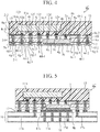
- FIG. 1 is a cross-sectional view illustrating structure of a high frequency circuit 1 according to Embodiment 1 of the present disclosure. As illustrated in FIG. 1 , the high frequency circuit 1 includes a printed wiring board 2 and a high frequency device 3.
- the printed wiring board 2 is a substrate constituting the high frequency circuit 1, and includes conductor layers 4a to 4h, a core layer 5, and a build-up layer 6.
- the conductor layers 4a to 4h are conductor layers formed in the core layer 5 and the build-up layer 6.
- the high frequency device 3 embodies a first high frequency device in the present disclosure.
- the high frequency device 3 is realized by, for example, a semiconductor chip which has a terminal surface 3a as one surface and a mirror surface 3b as another surface.
- the terminal surface 3a is a surface on which a terminal of the high frequency device 3 is installed.
- the mirror surface 3b, on which no terminal is formed, is a device back surface opposite the terminal surface 3a.
- the conductor layer 4g embodies a conductor layer for heat dissipation in the present disclosure, which has a ground potential.
- the conductor layer 4g is formed on one surface 2-1 of the printed wiring board 2 and faces an opening 5b from a lower surface side of the core layer 5.
- the conductor layer 4g is formed in the build-up layer 6 as a lowermost layer of the printed wiring board 2.
- One surface of the conductor layer 4g faces the outside, and another surface thereof faces the opening 5b.
- the conductor layer having a ground potential may be described as a ground conductor or a ground conductor layer
- a conductor layer for propagating a signal may be described as a signal conductor or a signal conductor layer.
- the conductor layer for heat dissipation by the conductor layer 4g is better to provide with one surface facing the outside of the printed wiring board 2, as illustrated in FIG. 1 .
- a ground conductor layer formed in an inner layer of the build-up layer 6 may be used for the conductor layer for heat dissipation.
- the conductor layer for heat dissipation has a multilayer structure in which a ground conductor layer facing the outside of the printed wiring board 2 is connected to the ground conductor layer in an inner layer of the build-up layer 6 through a via hole serving as a heat dissipation path.
- Each of the conductor layers 4a, 4b, and 4h embodies a terminal conductor layer in the present disclosure.
- Each layer is realized by a conductor layer formed on another surface 2-2 of the printed wiring board 2 and is electrically connected to a terminal of the high frequency device 3.
- the conductor layer 4h is a ground conductor layer formed on another surface 2-2 of the printed wiring board 2.
- the conductor layers 4a and 4b are signal conductor layers formed on the surface 2-2 of the printed wiring board 2, and a signal is propagated through the conductor layers 4a and 4b.
- the conductor layers 4c to 4f are ground conductor layers formed in the core layer 5.
- the core layer 5 embodies a first dielectric layer in the present disclosure.
- the core layer 5 is laminated to sandwich an insulating layer 5a with the conductor layers 4c to 4f.
- the core layer 5 has the opening 5b penetrating the core layer 5 in a layer thickness direction.
- the conductor layer 4c is electrically connected to the conductor layer 4d through a via hole 7 formed in the core layer 5, and the conductor layer 4d is electrically connected to the conductor layer 4g through a via hole 8 formed in the build-up layer 6.
- the conductor layer 4e is electrically connected to the conductor layer 4f through the via hole 7, and the conductor layer 4f is electrically connected to the conductor layer 4g through the via hole 8.
- the build-up layer 6 embodies a second dielectric layer in the present disclosure.
- the build-up layer 6 is laminated on each of one surface (lower surface) of the core layer 5 orthogonal to a layer thickness direction and another surface (upper surface) of the core layer 5 orthogonal to the layer thickness direction. Note that the build-up layer 6 and the via hole 8 are laminated by, for example, a build-up method.
- the high frequency device 3 is placed within the opening 5b of the core layer 5 such that the terminal surface 3a faces upward.
- the mirror surface 3b of the high frequency device 3 is bonded to the conductor layer 4g with an adhesive 10.
- the mirror surface 3b is thermally connected to the conductor layer 4g. It is desirable that the adhesive 10 has high thermal conductivity.
- the high frequency device 3 may be molded with resin while the mirror surface 3b and the conductor layer 4g are in contact with each other.
- a signal terminal 9a on the terminal surface 3a is electrically connected to the conductor layer 4a through the via hole 8 of the build-up layer 6.
- a signal terminal 9b of the terminal surface 3a is electrically connected to the conductor layer 4b through the via hole 8.
- the conductor layers 4a and 4b are signal conductor layers as described above.
- a ground terminal 9c on the terminal surface 3a is electrically connected to the conductor layer 4h through the via hole 8.
- the conductor layer 4h is a ground conductor layer as described above.
- a signal input to the conductor layer 4a is input to the high frequency device 3 through the via hole 8 and the signal terminal 9a. As a result, the high frequency device 3 processes the signal.
- a signal processed by the high frequency device 3 is output from the conductor layer 4b through the signal terminal 9b and the via hole 8. Heat generated during that time in the high frequency device 3 is dissipated from the mirror surface 3b to the outside through the adhesive 10 and the conductor layer 4g.
- the high frequency circuit 1 according to the Embodiment 1 includes the printed wiring board 2 and the high frequency device 3.
- the printed wiring board 2 includes the conductor layers 4a to 4h, the core layer 5 having the opening 5b penetrating the core layer 5 in a layer thickness direction, and the build-up layers 6 laminated on upper and lower surfaces of the core layer 5.
- the terminals 9a and 9b on the terminal surface 3a are electrically connected to the terminal conductor layers 4a, 4b, and 4h formed on an upper surface side of the core layer 5.
- the high frequency device 3 Since the high frequency device 3 is built in the printed wiring board 2 in this manner, the high frequency circuit 1 can be reduced in height, and a circuit having a small size can be realized.
- terminals are connected to each other with a short wiring distance through the via holes 8 formed in the build-up layer 6, a loss of input and output signals can be reduced.
- the mirror surface 3b of the high frequency device 3 is thermally connected to the conductor layer 4g. Therefore, high heat dissipation characteristics can be realized because a space of interposing a material having low thermal conductivity is narrowed.
- FIG. 2 is a cross-sectional view illustrating structure of a high frequency circuit 1A according to Embodiment 2 of the present disclosure.
- the same components as those in FIG. 1 are denoted by the same reference numerals, and description thereof is omitted.
- the high frequency circuit 1A includes a printed wiring board 2A, a high frequency device 3, and a high frequency device 11.
- the printed wiring board 2A is a substrate constituting the high frequency circuit 1A, and includes conductor layers 4a to 4k, a core layer 5, and a build-up layer 6A.
- the conductor layers 4a to 4k are conductor layers formed in the core layer 5 and the build-up layer 6A.
- the high frequency device 11 embodies a second high frequency device in the present disclosure.
- the high frequency device 11 is realized by, for example, a semiconductor chip having a terminal surface 11a as one surface and a mirror surface 11b as another surface.
- the terminal surface 11a is a surface on which a terminal of the high frequency device 11 is installed.
- the mirror surface 11b is a device back surface opposite the terminal surface 11a, on which no terminal is formed.
- the conductor layer 4g is a conductor layer for heat dissipation formed on one surface 2-1 of the printed wiring board 2A and facing an opening 5b from a lower surface side of the core layer 5.
- the conductor layers 4h, 4j, and 4k are ground conductor layers formed on another surface 2-2 of the printed wiring board 2A.
- the conductor layers 4a, 4b, and 4i are terminal conductor layers.
- the build-up layer 6A embodies a second dielectric layer in the present disclosure.
- the build-up layer 6A is laminated on each of an upper surface of the core layer 5 orthogonal to a layer thickness direction and a lower surface of the core layer 5 orthogonal to the layer thickness direction. Note that the build-up layer 6A and a via hole 8 are laminated by, for example, a build-up method.
- the high frequency device 11 is installed such that the terminal surface 11a facing another surface 2-2 of the printed wiring board 2A.
- a signal terminal 12a is electrically connected to the conductor layer 4a with solder 13
- a signal terminal 12d is electrically connected to the conductor layer 4i with solder 13.
- the conductor layers 4a and 4i are signal conductor layers.
- a ground terminal 12b is electrically connected to the conductor layer 4k with solder 13
- a ground terminal 12c is electrically connected to the conductor layer 4j with solder 13.
- a ground terminal 12e on the terminal surface 11a is electrically connected to the conductor layer 4h with solder 13. Note that the conductor layers 4k, 4j, and 4h are ground conductor layers.
- the conductor layers 4j and 4k are electrically connected to the conductor layer 4c of the core layer 5 through the via hole 8 of the build-up layer 6A.
- the conductor layer 4h is electrically connected to a ground terminal 9c of the high frequency device 3 through the via hole 8.
- the conductor layer 4i is electrically connected to a signal terminal 9a through the via hole 8.
- a signal input to the conductor layer 4a is input to the high frequency device 11 through solder 13 and the signal terminal 12a. As a result, the high frequency device 11 processes the signal.
- a signal processed by the high frequency device 11 is input to the high frequency device 3 through the signal terminal 12d, solder 13, the conductor layer 4i, the via hole 8, and the signal terminal 9a. As a result, the high frequency device 3 processes the signal.
- a signal processed by the high frequency device 3 is output from the conductor layer 4b through the signal terminal 9b and the via hole 8. Heat generated during that time in the high frequency device 3 is dissipated from the mirror surface 3b to the outside through the adhesive 10 and the conductor layer 4g.
- the high frequency device 11 is connected to the printed wiring board 2A only with solder 13.
- the high frequency device 11 may be further fixed by filling an under space thereof with an underfill 14.
- the high frequency device 11 may be connected to the printed wiring board 2A with an anisotropic conductive adhesive instead of solder 13, and an insulating adhesive may be used as the underfill 14.
- each of the high frequency circuits 1A and 1B according to the Embodiment 2 includes the high frequency device 11, which is installed such that the terminal surface 11a faces another surface 2-2 of the printed wiring board 2A.
- the high frequency device 11 is installed above the high frequency device 3. Therefore, a loss of input and output signals can be reduced because a wiring length between the high frequency device 3 and the high frequency device 11 is shortened.
- the high frequency device 3 is built in the printed wiring board 2A, a circuit having a small size can be realized even using a plurality of high frequency devices.
- the mirror surface 3b of the high frequency device 3 is thermally connected to the conductor layer 4g for heat dissipation. Therefore, high heat dissipation characteristics can be realized because a space of interposing a material having low thermal conductivity is narrowed.
- FIG. 4 is a cross-sectional view illustrating structure of a high frequency circuit 1C according to Embodiment 3 of the present disclosure.
- the high frequency circuit 1C includes a printed wiring board 2B, a high frequency device 3, and a high frequency device 11A. As illustrated in FIG. 4 , a surface 2-2 of the printed wiring board 2B including the high frequency device 11A is molded with resin 15.
- the printed wiring board 2B includes conductor layers 4a-1, 4b-1, 4b-2, 4c-1 to 4c-4, 4d-1 to 4d-4, 4e-1, 4e-2, 4f-1, 4f-2, 4g, 4g-1 to 4g-5, 4h to 4k, a core layer 5A, and a build-up layer 6B.
- the conductive layers 4a-1, 4b-1, 4b-2, 4c-1 to 4c-4, 4d-1 to 4d-4, 4e-1, 4e-2, 4f-1, 4f-2, 4g, 4g-1 to 4g-5, and 4h to 4k are conductor layers formed in the core layer 5A and the build-up layer 6B.
- the conductor layer 4g is a conductor layer for heat dissipation formed on a surface 2-1 of the printed wiring board 2B.
- the conductor layers 4a-1, 4b-2, 4c-1, 4c-2, 4c-4, 4d-1, 4d-2, 4d-4, 4e-2, 4f-2, 4g, 4g-1, 4g-2, 4g-5, 4h, and 4j are ground conductor layers.
- the conductor layers 4c-3, 4d-3, 4g-3, 4g-4, 4i, 4b-1, 4e-1, 4f-1, and 4k are signal conductor layers.
- the conductor layers 4c-1 to 4c-4 are electrically connected to the conductor layers 4d-1 to 4d-4 through a via hole 7 formed in the core layer 5A.
- the conductor layer 4d-4 is electrically connected to the conductor layer 4g through a via hole 8 formed in the build-up layer 6B.
- the conductor layers 4e-1 and 4e-2 are electrically connected to the conductor layers 4f-1 and 4f-2 through the via hole 7.
- the conductor layers 4f-1 and 4f-2 are electrically connected to the conductor layers 4g-4 and 4g-5 through the via hole 8.
- the core layer 5A embodies a first dielectric layer in the present disclosure.
- the core layer 5A is laminated to sandwich an insulating layer 5a with the conductor layers 4c-1 to 4c-4, 4d-1 to 4d-4, 4e-1, 4e-2, 4f-1, and 4f-2.
- the core layer 5A has an opening 5b penetrating the core layer 5A in a layer thickness direction.
- the build-up layer 6B embodies a second dielectric layer in the present disclosure.
- the build-up layer 6B is laminated on each of an upper surface of the core layer 5A orthogonal to a layer thickness direction and a lower surface of the core layer 5A orthogonal to the layer thickness direction.
- the build-up layer 6B and the via hole 8 are laminated by, for example, a build-up method.
- the high frequency device 11A embodies a second high frequency device in the present disclosure.
- the high frequency device 11A is installed such that a terminal surface 11a faces the surface 2-2 of the printed wiring board 2B.
- a signal terminal 12f is electrically connected with solder 13 to the conductor layer 4k being a signal conductor
- a signal terminal 12d is electrically connected with solder 13 to the conductor layer 4i being a signal conductor.
- a ground terminal 12g is electrically connected with solder 13 to the conductor layer 4a-1 being a ground conductor layer
- a ground terminal 12c is electrically connected with solder 13 to the conductor layer 4j being a ground conductor.
- a ground terminal 12e is electrically connected with solder 13 to the conductor layer 4h being a ground conductor.
- a signal input to the conductor layer 4g-3 is input to the core layer 5A through the via hole 8 and the conductor layer 4d-3, and, after that, input to the high frequency device 11A through the via hole 7, the conductor layer 4c-3, the via hole 8, the conductor layer 4k, solder 13, and the signal terminal 12f.
- the high frequency device 11A processes the signal.
- a signal processed by the high frequency device 11A is input to the high frequency device 3 through the signal terminal 12d, solder 13, the conductor layer 4i, the via hole 8, and the signal terminal 9a. As a result, the high frequency device 3 processes the signal.
- a signal processed by the high frequency device 3 is input to the core layer 5A through the signal terminal 9b, the via hole 8, the conductor layer 4b-1, the via hole 8, and the conductor layer 4e-1, and output from the conductor layer 4g-4 through the via hole 7, the conductor layer 4f-1, and the via hole 8.
- Heat generated during that time in the high frequency device 3 is dissipated from the mirror surface 3b to the outside through the adhesive 10 and the conductor layer 4g.
- the high frequency device 11A may be fixed by filling an under space thereof with an underfill 14 before being molded with resin 15.
- the high frequency device 11A may be connected to the printed wiring board 2B with an anisotropic conductive adhesive instead of solder 13, and an insulating adhesive may be used as the underfill 14.
- the high frequency circuit 1C may be installed on a mother board 16.
- conductor layers 17a and 17b provided in the mother board 16 are signal conductor layers, and are connected to the high frequency circuit 1C through a via hole 18.
- conductor layers 17c, 17d, and 17e provided in the mother board 16 are ground conductor layers, and are connected to one another through a plurality of via holes 18 penetrating the mother board 16 in a layer thickness direction.
- Heat generated in the high frequency device 3 is transferred to the conductor layer 17c of the mother board 16 through the conductor layer 4g and solder 13, and, after that, dissipated from the conductor layer 17e through the conductor layer 17d and the via holes 18 formed above and below the conductor layer 17d. Therefore, in the high frequency circuit 1C illustrated in FIG. 5 , a conductor layer for heat dissipation is formed by the conductor layer 4g, solder 13, the conductor layers 17c to 17e, and the via hole 18.
- a metal block 19 may be provided between the conductor layer 17c and the conductor layer 17e in the mother board 16.
- the metal block 19 is in contact with the conductor layers 17c and 17e. As a result, heat generated in the high frequency device 3 is dissipated from the conductor layer 17e through the conductor layer 17c and the metal block 19.
- a conductor layer for heat dissipation is formed by the conductor layer 4g, solder 13, the conductor layer 17c, the metal block 19, and the conductor layer 17e.
- Embodiment 3 may be applied to the structure described in the foregoing Embodiment 2.
- the high frequency device 11 may be molded with the resin 15. Even with such structure, an effect similar to the above can be obtained.
- the high frequency device 11A is molded with the resin 15. With such structure, in addition to the effect described in the Embodiment 2, reliability of mounting is improved by molding with the resin 15.
- the high frequency circuit 1C has structure, in which a signal is transmitted toward the surface 2-1 of the printed wiring board 2B, the high frequency circuit 1C can be used as a surface mounting package.
- FIG. 7 is a cross-sectional view illustrating structure of a high frequency circuit 1D according to Embodiment 4 of the present disclosure.
- the high frequency circuit 1D includes a printed wiring board 2B, a high frequency device 3, and a high frequency device 11A.
- a surface 2-2 of the printed wiring board 2B including the high frequency device 11A is molded with resin 15.
- the high frequency circuit 1D In the high frequency device 11A in the high frequency circuit 1D, a mirror surface 11b is exposed from the resin 15 as illustrated in FIG. 7 . Specifically, in the high frequency circuit 1D, the resin 15 is molded up to a height equal to or lower than that of the mirror surface 11b in a thickness direction of the high frequency device 11A. According to this structure, the high frequency circuit 1D is thinner than the high frequency circuit 1C illustrated in FIG. 5 .
- the high frequency circuit 1D operates similarly to the high frequency circuit 1C described in the foregoing Embodiment 3. During this operation, heat generated in the high frequency device 3 is dissipated from a conductor layer 4g to the outside through a mirror surface 3b and an adhesive 10. Heat generated in the high frequency device 11A is dissipated from the mirror surface 11b to the outside.
- the high frequency device 11A may be fixed by filling an under space thereof with an underfill 14 before being molded with resin 15.
- the high frequency device 11A may be connected to the printed wiring board 2B with an anisotropic conductive adhesive instead of solder 13, and an insulating adhesive may be used as the underfill 14.
- the high frequency circuit 1D may be mounted on the mother board 16 illustrated in FIGS. 5 and 6 .
- the Embodiment 4 may be applied to the structure described in the foregoing Embodiment 2. That is, in the high frequency circuits 1A and 1B according to the Embodiment 2, molding may be performed with the resin 15 to expose the mirror surface 11b of the high frequency device 11.
- the mirror surface 11b of the high frequency device 11A is exposed from the resin 15.
- FIG. 8 is a cross-sectional view illustrating structure of a high frequency circuit 1E according to Embodiment 5 of the present disclosure.
- the high frequency circuit 1E includes a printed wiring board 2B, a high frequency device 3, and a high frequency device 11A.
- a surface 2-2 of the printed wiring board 2B including the high frequency device 11A is molded with resin 15.
- a metal plate 20 is connected to a mirror surface 11b with an adhesive 10a. It is desirable that the adhesive 10a has high thermal conductivity like the adhesive 10.
- the metal plate 20 is exposed from the resin 15 to the outside.
- the resin 15 is molded up to a height equal to or lower than that of a surface of the metal plate 20 in a thickness direction of the high frequency device 11A.
- the high frequency circuit 1E has substantially the same thickness as the high frequency circuit 1D, and is thinner than the high frequency circuit 1C illustrated in FIG. 5 .
- the high frequency circuit 1E operates similarly to the high frequency circuit 1C described in the foregoing Embodiment 3. In this operation, heat generated in the high frequency device 3 is dissipated from a mirror surface 3b to the outside through the adhesive 10 and a conductor layer 4g. In addition, heat generated in the high frequency device 11A is dissipated from the mirror surface 11b to the outside through the adhesive 10a and the metal plate 20.
- the high frequency device 11A may be fixed by filling an under space thereof with an underfill 14 before being molded with resin 15.
- the high frequency device 11A may be connected to the printed wiring board 2B with an anisotropic conductive adhesive instead of solder 13, and an insulating adhesive may be used as the underfill 14.
- the high frequency circuit 1E may be installed on a mother board 16.
- Embodiment 5 may be applied to the structure described in the foregoing Embodiment 2.
- the metal plate 20 may be connected to the mirror surface 11b of the high frequency device 11, and the molding with the resin 15 may be performed to expose the metal plate 20. Even with such structure, an effect similar to the above can be obtained.
- the high frequency circuit 1E according to the Embodiment 5 includes the metal plate 20 connected to the mirror surface 11b of the high frequency device 11A, and the metal plate 20 is exposed from the resin 15. With such structure, in addition to the effect described in the Embodiment 3, a thin circuit can be realized. In addition, since heat generated in the high frequency device 11A is dissipated from the metal plate 20, the property of heat dissipation is improved.
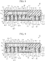
- FIG. 9 is a cross-sectional view illustrating structure of a high frequency circuit IF according to Embodiment 6 of the present disclosure.
- the high frequency circuit IF includes a printed wiring board 2B, a high frequency device 3, and a high frequency device 11A.
- a surface 2-2 of the printed wiring board 2B including the high frequency device 11A is molded with resin 15.
- a shield 21 is provided on a mirror surface 11b of the high frequency device 11A in the high frequency circuit IF, as illustrated in FIG. 9 .
- the shield 21 embodies a first shield in the present disclosure.
- the shield 21 covers the mirror surface 11b of the high frequency device 11A and a surface of the resin 15 provided around the mirror surface 11b.
- the shield 21 is formed by, for example, performing metal-plating on the mirror surface 11b and the surface of the resin 15.
- a conductive thin film obtained by printing, spraying, or sealing a conductive material on the mirror surface 11b and the surface of the resin 15 may be provided as the shield 21.
- the shield 21 is electrically connected to a ground conductor layer of the printed wiring board 2B.
- the shield 21 covers a side of the surface 2-2 of the printed wiring board 2B while being in contact with conductor layers 4a-1 and 4b-2 of a ground conductor.
- FIG. 10 is a top view illustrating the high frequency circuit IF, in which the high frequency device 11A and a conductor layer 4b-1 covered with the resin 15 are represented by broken lines.
- an area including the high frequency device 11A and the conductor layer 4b-1 and being surrounded by the conductor layers 4a-1 and 4b-2 is molded with the resin 15, as illustrated in FIG. 10 .
- the shield 21 is formed by performing metal-plating on the surface 2-2 of the printed wiring board 2B.
- the shield 21 is also formed on the conductor layers 4a-1 and 4b-2, and the shield 21 is electrically connected to the conductor layers 4a-1 and 4b-2.
- the high frequency circuit IF operates similarly to the high frequency circuit 1C described in the foregoing Embodiment 3. In this operation, heat generated in the high frequency device 3 is dissipated from a mirror surface 3b to the outside through the adhesive 10 and a conductor layer 4g. In addition, heat generated in the high frequency device 11A is dissipated from the mirror surface 11b through the shield 21.
- a signal is propagated in the high frequency circuit IF, one surface of the high frequency circuit IF is covered with the shield 21 having a ground potential. Therefore, an unnecessary electromagnetic wave is hardly radiated to the outside of the high frequency circuit IF.
- the high frequency device 11A may be fixed by filling an under space thereof with an underfill 14 before being molded with resin 15.
- the high frequency device 11A may be connected to the printed wiring board 2B with an anisotropic conductive adhesive instead of solder 13, and an insulating adhesive may be used as the underfill 14.
- the high frequency circuit IF may be installed on a mother board 16.
- Conductor layers 17a and 17b provided on the mother board 16 are connected to the high frequency circuit IF through a via hole 18.
- the conductor layer 4g of the high frequency circuit IF is connected to a conductor layer 17c of the mother board 16 with solder 13.
- the conductor layer 17c is connected to conductor layers 17d and 17e through a plurality of the via holes 18.
- Heat generated in the high frequency device 3 is transferred to the conductor layer 17c of the mother board 16 through the conductor layer 4g and solder 13, and is further dissipated from the conductor layer 17e through the conductor layer 17d and the via holes 18 formed above and below the conductor layer 17d.
- a conductor layer for heat dissipation is formed by the conductor layer 4g, solder 13, the conductor layers 17c to 17e, and the via hole 18.
- the high frequency circuit IF may be installed on the mother board 16 in which the metal block 19 illustrated in FIG. 6 is provided.
- Embodiment 6 may be applied to the structure disclosed in the foregoing Embodiment 2.
- the molding may be performed with the resin 15 to expose the mirror surface 11b of the high frequency device 11.
- the mirror surface 11b and the surface 2-2 including a surface of the resin 15 around the mirror surface 11b may be covered with the shield 21. Even with such structure, an effect similar to the above can be obtained.
- FIG. 12 is a top view illustrating an arrangement of terminals in the high frequency devices 3 and 11A.
- FIG. 12 in order to visually represent the arrangement of the terminals, representations other than the outer shape of the high frequency device 11A and the terminals are illustrated transparently.
- a circle surrounding a letter "S” indicates a signal terminal
- a circle surrounding a letter “G” indicates a ground terminal.
- ground terminals are arranged around a signal terminal.
- the ground terminals are arranged at intervals designed to reduce leakage of a high frequency signal in a usable frequency band of the high frequency circuit IF.
- the ground terminals are arranged at intervals that are capable of making a cutoff frequency higher than that in the usable frequency band. With such structure, it is possible to reduce leakage of an unnecessary high frequency signal to elements other than a signal path passing through a signal terminal.
- the ground terminals are arranged around a signal terminal on both the terminal surface 3a of the high frequency device 3 and the terminal surface 11a of the high frequency device 11A.
- the ground terminals may be arranged around a signal terminal on either the terminal surface 3a or the terminal surface 11a.
- the arrangement where ground terminals are arranged around a signal terminal may be applied to the high frequency device 3 included in the high frequency circuit 1 according to the foregoing Embodiment 1. Even with such structure, an effect similar to the above can be obtained.
- the high frequency circuit IF according to the Embodiment 6 includes the shield 21 that covers the mirror surface 11b of the high frequency device 11A and the resin 15 and is electrically connected to the conductor layers 4a-1 and 4b-2 of a ground conductor.
- the ground terminals are arranged around a signal terminal at intervals designed to reduce leakage of a high frequency signal in the usable frequency band.
- FIG. 13 is a cross-sectional view illustrating structure of a high frequency circuit 1G according to Embodiment 7 of the present disclosure.
- the high frequency circuit 1G includes a printed wiring board 2B, a high frequency device 3, and a high frequency device 11A.
- a surface 2-2 of the printed wiring board 2B including the high frequency device 11A is molded with resin 15.
- a metal plate 20 is bonded to a mirror surface 11b with an adhesive 10a.
- the mirror surface 11b is thermally connected to the metal plate 20.
- the adhesive 10a is desirably an adhesive having high thermal conductivity like the adhesive 10.
- the metal plate 20 is exposed from the resin 15 covering the high frequency device 11A.
- the entire surface 2-2 including an exposed part of the metal plate 20 and the resin 15 provided around the metal plate 20 are covered with a shield 21A.
- the resin 15 is molded up to a height equal to or lower than that of a surface of the metal plate 20 in a thickness direction of the high frequency device 11A.
- the high frequency circuit 1G has substantially the same thickness as the high frequency circuit 1E illustrated in FIG. 8 , and is slightly thinner than the high frequency circuit 1C illustrated in FIG. 5 .
- the shield 21A embodies a second shield in the present disclosure.
- the shield 21A covers a side of the surface 2-2 of the printed wiring board 2B while contacting conductor layers 4a-1 and 4b-2.
- the shield 21A is formed by, for example, performing metal-plating on the mirror surface 11b of the high frequency device 11A and a surface of the resin 15 like the foregoing shield 21.
- a conductive thin film which is obtained by printing, spraying, or sealing a conductive material on the mirror surface 11b of the high frequency device 11A and the surface of the resin 15, may be used as the shield 21A.
- the high frequency circuit 1G operates similarly to the high frequency circuit 1C described in the foregoing Embodiment 3. In this operation, heat generated in the high frequency device 3 is dissipated from a mirror surface 3b to the outside through the adhesive 10 and a conductor layer 4g.
- heat generated in the high frequency device 11A is dissipated from the mirror surface 11b to the outside through the adhesive 10a, the metal plate 20 and the shield 21.
- the high frequency device 11A may be fixed by filling an under space thereof with an underfill 14 before being molded with resin 15.
- the high frequency device 11A may be connected to the printed wiring board 2B with an anisotropic conductive adhesive instead of solder 13, and an insulating adhesive may be used as the underfill 14.
- the high frequency circuit 1G may be installed on the mother board 16 illustrated in FIGS. 5 and 6 .
- Embodiment 7 may be applied to the structure described in the foregoing Embodiment 2.
- the metal plate 20 may be connected to the mirror surface 11b of the high frequency device 11, the molding may be performed with the resin 15 to expose the metal plate 20, and the shield 21 may be provided on a surface of the molded product. Even with such structure, an effect similar to the above can be obtained.
- ground terminals may be arranged around a signal terminal at intervals that are designed to prevent leakage of a high frequency signal in a usable frequency band of the high frequency circuit 1G. As a result, it is possible to reduce leakage of an unnecessary high frequency signal to elements other than a signal path passing through a signal terminal.
- the high frequency circuit 1G according to the Embodiment 7 includes the shield 21A covering the metal plate 20 and the resin 15 and is electrically connected to the conductor layers 4a-1 and 4b-2, each having a ground potential.
- the metal plate 20 having a low thermal resistance is provided near the high frequency device 11A, there is an effect that the property of heat dissipation is improved in addition to the effect described in the foregoing Embodiment 6.
- FIG. 14 is a cross-sectional view illustrating structure of a high frequency circuit 1H according to an Embodiment 8 of the present disclosure.
- the high frequency circuit 1H includes a printed wiring board 2B, a high frequency device 3, and a high frequency device 11B.
- a surface 2-2 of the printed wiring board 2B including the high frequency device 11B is molded with resin 15.
- the high frequency device 11B embodies a second high frequency device in the present disclosure.
- a conductor layer 22 having a ground potential is formed on a mirror surface 11b being a device back surface.
- a ground terminal on a terminal surface 11a is electrically connected to the conductor layer 22 through a via hole 23 penetrating the high frequency device 11B in a thickness direction.
- a shield 21B covers the conductor layer 22 on the mirror surface 11b and a surface of the resin 15 provided around the conductor layer 22 while contacting conductor layers 4a-1 and 4b-2, each having a ground potential.
- the shield 21B is formed by, for example, performing metal-plating on the conductor layer 22 of the high frequency device 11B and the surface of the resin 15.
- a conductive thin film obtained by printing, spraying, or sealing a conductive material on the conductor layer 22 of the high frequency device 11B and the surface of the resin 15 may be used as the shield 21B.
- the high frequency circuit 1H operates similarly to the high frequency circuit 1C described in the foregoing Embodiment 3. In this operation, heat generated in the high frequency device 3 is dissipated from a mirror surface 3b to the outside through the adhesive 10 and a conductor layer 4g.
- heat generated in the high frequency device 11B is dissipated from the mirror surface 11b to the outside through the conductor layer 22 and the shield 21B.
- FIG. 15 is a top view illustrating the high frequency circuit 1H, in which the high frequency device 11B and a conductor layer 4b-1 covered with the resin 15 are represented by broken lines.
- a ground terminal on a terminal surface 11a is electrically connected to the conductor layer 22 through a plurality of via holes 23 provided at a plane perpendicular to a thickness direction.
- a space of a ground potential formed by the shield 21B covering the high frequency device 11B is electromagnetically divided into a plurality of small spaces by the via holes 23. In each of the small spaces, a resonance frequency shifts to a higher frequency, and thus oscillation of the high frequency device 11B is suppressed.
- a ground conductor layer may be provided on the mirror surface 11b of the high frequency device 11.
- a ground terminal on the terminal surface 11a of the high frequency device 11 is electrically connected to the above-mentioned conductor layer through a via hole penetrating the high frequency device 11 in a thickness direction.
- the high frequency device 11B may be fixed by filling an under space thereof with an underfill 14 before being molded with resin 15.
- the high frequency device 11B may be connected to the printed wiring board 2B with an anisotropic conductive adhesive instead of solder 13, and an insulating adhesive may be used as the underfill 14.
- the high frequency circuit 1H may be installed on the mother board 16 illustrated in FIGS. 5 and 6 .
- Embodiment 8 may be applied to the structure described in the foregoing Embodiment 2.
- the conductor layer 22 may be formed on the mirror surface 11b of the high frequency device 11, and the shield 21B may be provided on the conductor layer 22 and the resin 15 after the molding may be performed with the resin 15 to expose the conductor layer 22. Even with such structure, an effect similar to the above can be obtained.
- ground terminals may be arranged around a signal terminal at intervals designed to reduce leakage of a high frequency signal in a usable frequency band. As a result, it is possible to reduce leakage of an unnecessary high frequency signal to elements other than a signal path passing through a signal terminal.
- the conductor layer 22 being a ground conductor layer is formed on the mirror surface 11b of the high frequency device 11B.
- a ground terminal on the terminal surface 11a is electrically connected to the conductor layer 22 through the via hole 23 penetrating the high frequency device 11B in a thickness direction.
- a space having a ground potential formed by the shield 21B covering the high frequency device 11B is electromagnetically divided into small spaces by the via hole 23.
- FIG. 16 is a cross-sectional view illustrating structure of a high frequency circuit 1I according to Embodiment 9 of the present disclosure.
- the high frequency circuit 1I includes a printed wiring board 2B, a high frequency device 3, and a high frequency device 11A.
- a surface 2-2 of the printed wiring board 2B including the high frequency device 11A is covered with a metal cap 24.
- the metal cap 24 is a hollow metal member having an opening.
- the metal cap 24 is provided such that the opened part thereof faces the surface 2-2 of the printed wiring board 2B.
- the metal cap 24 is in contact with conductor layers 4a-1 and 4b-2 being ground conductors while being disposed on the printed wiring board 2B.
- the high frequency circuit 1I operates similarly to the high frequency circuit 1C disclosed in the foregoing Embodiment 3. In this operation, heat generated in the high frequency device 3 is dissipated from a mirror surface 3b to the outside through the adhesive 10 and a conductor layer 4g. In addition, heat generated in the high frequency device 11A is dissipated from a mirror surface 11b to the hollow part covered with the metal cap 24.
- the high frequency device 11A may be fixed by filling an under space thereof with an underfill 14 before being molded with resin 15.
- the high frequency device 11A may be connected to the printed wiring board 2B with an anisotropic conductive adhesive instead of solder 13, and an insulating adhesive may be used as the underfill 14.
- the high frequency circuit 1I may be installed on the mother board 16 illustrated in FIGS. 5 and 6 .
- Embodiment 9 may be applied to the structure described in the foregoing Embodiment 2.
- the metal cap 24 may be provided to each of the high frequency circuits 1A and 1B according to the Embodiment 2. Even with such structure, an effect similar to the above can be obtained.
- ground terminals may be arranged around a signal terminal at intervals designed to reduce leakage of a high frequency signal in a usable frequency band.
- the high frequency circuit 1I according to the Embodiment 9 includes the metal cap 24 that covers the surface 2-2 of the printed wiring board 2B and is electrically connected to the conductor layers 4a-1 and 4b-2 being ground conductors. In this way, since a space between the metal cap 24 and a mounting surface of the high frequency device 11A is hollow, a dielectric loss can be reduced.
- FIG. 17 is a cross-sectional view illustrating structure of a high frequency circuit 1J according to Embodiment 10 of the present disclosure.
- the high frequency circuit 1J includes a printed wiring board 2C, a high frequency device 3, and a high frequency device 11A.
- a surface 2-2 of the printed wiring board 2C including the high frequency device 11A is molded with resin 15.
- a mirror surface 11b exposed from the resin 15 and a surface of the resin 15 around the mirror surface 11b are covered with a shield 21.
- the printed wiring board 2C is a substrate constituting the high frequency circuit 1J according to the Embodiment 10.
- the printed wiring board 2C includes a core layer 5A and a build-up layer 6C.
- Conductor layers 4a-1, 4b-1, 4b-2, 4c-1 to 4c-4, 4d-1 to 4d-4, 4e-1, 4e-2, 4f-1, 4f-2, 4g, 4g-1 to 4g-5, 4h to 4k, and 41-1 to 41-5 are formed in the core layer 5A and the build-up layer 6C.
- the core layer 5A embodies a first dielectric layer in the present disclosure.
- the core layer 5A is laminated to sandwich an insulating layer 5a with the conductor layers 4c-1 to 4c-4, 4d-1 to 4d-4, 4e-1, 4e-2, 4f-1, and 4f-2, and has an opening 5b penetrating the core layer 5A in a layer thickness direction.
- the build-up layer 6C embodies a second dielectric layer in the present disclosure.
- Two build-up layers 6C are laminated on an upper surface of the core layer 5A orthogonal to a layer thickness direction, and one build-up layer 6C is laminated on a lower surface of the core layer 5A orthogonal to the layer thickness direction.
- the build-up layer 6C and a via hole 8 are laminated by, for example, a build-up method.
- the conductor layers 4c-1 to 4c-4, 4e-1, and 4e-2 are formed on an upper surface side of the core layer 5A, and the conductor layers 4d-1 to 4d-4, 4f-1, and 4f-2 are formed on a lower surface side of the core layer 5A.
- the conductor layers 4g and 4g-1 to 4g-5 are formed in the build-up layer 6C on the lower surface side of the core layer 5A.
- the conductor layers 4a-1, 4b-1, 4b-2, and 4h to 4k are provided in the first build-up layer 6C from an upper surface of the core layer 5A, and the conductor layers 41-1 to 41-5 are provided in the second build-up layer 6C from the upper surface of the core layer 5A.
- the conductor layers 4c-1 to 4c-4 are electrically connected to the conductor layers 4d-1 to 4d-4 through a via hole 7 formed in the core layer 5A.
- the conductor layers 4d-1 to 4d-4 are electrically connected to the conductor layers 4g-1 to 4g-3 and 4g through a via hole 8 formed in the build-up layer 6C.
- the conductor layers 4e-1 and 4e-2 are electrically connected to the conductor layers 4f-1 and 4f-2 through the via hole 7, and the conductor layers 4f-1 and 4f-2 are electrically connected to the conductor layers 4g-4 and 4g-5 through the via hole 8.
- the conductor layers 4c-1 and 4c-2 are electrically connected to the conductor layer 4a-1 through the via hole 8 formed in the first build-up layer 6C from the upper surface of the core layer 5A.
- the conductor layers 4c-3 and 4c-4 are electrically connected to the conductor layers 4k and 4j through the via hole 8 of the first layer
- the conductor layers 4e-1 and 4e-2 are electrically connected to the conductor layers 4b-1 and 4b-2.
- the conductor layer 4a-1 is electrically connected to the conductor layer 41-1 through the via hole 8 formed in the second build-up layer 6C from the upper surface of the core layer 5A.
- the conductor layer 4b-2 is electrically connected to the conductor layer 41-5
- the conductor layer 4h is electrically connected to the conductor layer 41-5
- the conductor layer 4i is electrically connected to the conductor layer 41-4.
- the conductor layer 4j is electrically connected to the conductor layer 41-3
- the conductor layer 4k is electrically connected to the conductor layer 41-2.
- the high frequency device 3 is placed within the opening 5b of the core layer 5A with a terminal surface 3a facing upward.
- the mirror surface 3b of the high frequency device 3 is bonded to the conductor layer 4g with an adhesive 10.
- the adhesive 10 is desirably an adhesive having high thermal conductivity.
- a signal terminal 9a on the terminal surface 3a is electrically connected to the conductor layer 4i being a signal conductor through the via hole 8 of the first layer
- a signal terminal 9b on the terminal surface 3a is electrically connected to the conductor layer 4b-1 being a signal conductor through the via hole 8 of the first layer
- a ground terminal 9c on the terminal surface 3a is electrically connected to the conductor layer 4h being a ground conductor through the via hole 8 of the first layer.
- the conductor layers 4h and 4j being ground conductors are provided around the conductor layer 4i being a signal conductor layer
- the conductor layers 4h and 4b-2 being ground conductors are provided around the conductor layer 4b-1 being a signal conductor.
- the conductor layers 41-3 and 41-5 being ground conductors are provided around the conductor layer 41-4 being a signal conductor.
- the conductor layers 4g and 4g-5 being ground conductors are provided around the conductor layer 4g-4 being a signal conductor.
- a signal input to the conductor layer 4g-3 is input to the core layer 5A through the via hole 8 and the conductor layer 4d-3, and input to the conductor layer 4k in the first build-up layer 6C from the upper surface of the core layer 5A through the via hole 7, the conductor layer 4c-3, and the via hole 8.
- the above-mentioned signal is input to the conductor layer 41-2 in the second build-up layer 6C from the upper surface of the core layer 5A through the via hole 8, and input to the high frequency device 11A through solder 13 and a signal terminal 12f.
- the high frequency device 11A processes the signal. Heat generated in the high frequency device 11A during that time is dissipated from the mirror surface 11b to the outside through the shield 21.
- a signal processed by the high frequency device 11A is input to the conductor layer 4i through a signal terminal 12d, solder 13, the conductor layer 41-4, and the via hole 8.
- the signal is input to the high frequency device 3 through the via hole 8 and the signal terminal 9a.
- the high frequency device 3 processes the signal.
- a signal processed by the high frequency device 3 is input to the core layer 5A through the signal terminal 9b, the via hole 8, the conductor layer 4b-1, and the via hole 8.
- the above-mentioned signal is output from the core layer 5A through the conductor layer 4e-1, the via hole 7, and the conductor layer 4f-1, and output from the conductor layer 4g-4 through the via hole 8. Heat generated in the high frequency device 3 during that time is dissipated from the mirror surface 3b to the outside through the adhesive 10 and the conductor layer 4g.
- the conductor layer 4b-1 being a signal conductor is surrounded by the conductor layers 4h, 41-5, 4b-2, and 4e-2 being ground conductors
- the conductor layer 4g-4 being a signal conductor is surrounded by the conductor layers 4g and 4g-5 being ground conductors.
- the high frequency device 11A may be fixed by filling an under space thereof with an underfill 14 before being molded with resin 15.
- the high frequency device 11A may be connected to the printed wiring board 2C with an anisotropic conductive adhesive instead of solder 13, and an insulating adhesive may be used as the underfill 14.
- the high frequency circuit 1J may be installed on the mother board 16 illustrated in FIGS. 5 and 6 .
- ground terminals may be arranged around a signal terminal at intervals designed to reduce leakage of a high frequency signal in a usable frequency band.
- the conductor layers 4j, 4h, and 4b-2 being ground conductors are provided around the conductor layers 4i and 4b-1 being signal conductors
- the conductor layers 41-3 and 41-5 being ground conductors are provided around the conductor layer 41-4 being a signal conductor.
- FIG. 18 is a cross-sectional view illustrating structure of a high frequency circuit 1K according to an Embodiment 11 of the present disclosure.
- the high frequency circuit 1K includes a printed wiring board 2D, a high frequency device 3, and a high frequency device 11A.
- a surface 2-2 of the printed wiring board 2D including the high frequency device 11A is molded with resin 15.
- a mirror surface 11b exposed from the resin 15 and a surface of the resin 15 around the mirror surface 11b are covered with a shield 21.
- the printed wiring board 2D is a substrate of the high frequency circuit 1K according to the Embodiment 11, and includes a core layer 5A and a build-up layer 6D.
- the printed wiring board 2D includes conductor layers 4a-1, 4b-1, 4b-2, 4c-1 to 4c-4, 4d-1 to 4d-4, 4e-1, 4e-2, 4f-1, 4f-2, 4g, 4g-1 to 4g-5, 4h to 4k, 41-1 to 41-5, and 4m-1 to 4m-6.
- the build-up layer 6D embodies a second dielectric layer in the present disclosure.
- Two build-up layers 6D are laminated on an upper surface of the core layer 5A orthogonal to a layer thickness direction, and another two build-up layers 6D are laminated on a lower surface of the core layer 5A orthogonal to the layer thickness direction.
- the build-up layer 6C and a via hole 8 are laminated by, for example, a build-up method. Since the build-up layer 6D is laminated on the upper surface of the core layer 5A with the same number of layers as on the lower surface thereof, it is possible to reduce warpage of the printed wiring board 2D due to a vertically symmetrical layer structure.
- the conductor layers 4m-1 to 4m-6 are formed in the lowermost build-up layer 6D laminated on a lower surface side of the core layer 5A.
- the conductor layers 4d-1 to 4d-3 are electrically connected to the conductor layers 4m-1 to 4m-3 through the via hole 8 while interposing the conductor layers 4g-1 to 4g-3 therebetween.
- the conductor layer 4g is electrically connected to the conductor layer 4m-4 through a plurality of the via holes 8.
- the conductor layers 4g-4 and 4g-5 are electrically connected to the conductor layers 4m-5 and 4m-6 through the via hole 8.
- the conductor layer 4m-4 is a ground conductor layer having one surface facing the outside of the printed wiring board 2D and another surface facing the conductor layer 4g.
- the plurality of via holes 8 is formed between the conductor layer 4m-4 and the conductor layer 4g, and the via holes 8 serve as heat dissipation paths.
- the conductor layer 4g and the conductor layer 4m-4 connected to each other through the via hole 8 is a conductor layer for heat dissipation.
- the conductor layer 4m-5 is a signal conductor layer.
- the conductor layers 4m-4 and 4m-6 being ground conductors are provided around the conductor layer 4m-5 as illustrated in FIG. 18 .
- a signal input to the conductor layer 4m-3 is input to the core layer 5A through the via hole 8, the conductor layer 4g-3, the via hole 8, and the conductor layer 4d-3, and further input to the conductor layer 4k in the build-up layer 6D through the via hole 7, the conductor layer 4c-3, and the via hole 8.
- the above-mentioned signal is input to the conductor layer 41-2 through the via hole 8, and input to the high frequency device 11A through solder 13 and a signal terminal 12f.
- the high frequency device 11A processes the signal. Heat generated in the high frequency device 11A during that time is dissipated from the mirror surface 11b to the outside through the shield 21.
- a signal processed by the high frequency device 11A is input to the conductor layer 4i through a signal terminal 12d, solder 13, the conductor layer 41-4, and the via hole 8.
- the above-mentioned signal is input to the high frequency device 3 through the via hole 8 and the signal terminal 9a.
- the high frequency device 3 processes the signal.
- a signal processed by the high frequency device 3 is input to the conductor layer 4b-1 through a signal terminal 9b and the via hole 8 and input to the core layer 5A through the via hole 8.
- the signal is output from the core layer 5A through the conductor layer 4e-1, the via hole 7, and the conductor layer 4f-1, and output from the conductor layer 4m-5 through the via hole 8, the conductor layer 4g-4, and the via hole 8.
- Heat generated in the high frequency device 3 during that time is dissipated from a mirror surface 3b to the outside through an adhesive 10, the conductor layer 4g, the via hole 8, and the conductor layer 4m-4.
- the conductor layer 4b-1 being a signal conductor is surrounded by the conductor layers 4h, 41-5, 4b-2, and 4e-2 being ground conductors.
- the conductor layer 4g-4 being a signal conductor is surrounded by the conductor layers 4g and 4g-5 being ground conductors, and the conductor layer 4m-5 being a signal conductor is surrounded by the conductor layers 4m-4 and 4m-6 being ground conductors.
- the high frequency device 11A may be fixed by filling an under space thereof with an underfill 14 before being molded with resin 15.
- the high frequency device 11A may be connected to the printed wiring board 2D with an anisotropic conductive adhesive instead of solder 13, and an insulating adhesive may be used as the underfill 14.
- the high frequency circuit 1K may be installed on the mother board 16 illustrated in FIGS. 5 and 6 .
- ground terminals may be arranged around a signal terminal at intervals designed to reduce leakage of a high frequency signal in a usable frequency band. As a result, it is possible to reduce leakage of an unnecessary high frequency signal to elements other than a signal path passing through a signal terminal.
- two built-up layers 6D are laminated on each of the upper and lower surfaces of the core layer 5A.
- three or more build-up layers may be laminated.
- the high frequency circuit 1K according to the Embodiment 11 it is only required to laminate the build-up layer 6D on the upper surface of the core layer 5A with the same number of layers as on the lower surface thereof.
- the build-up layer 6D is laminated on the upper surface of the core layer 5A with the same number of layers as on the lower surface thereof.
- the embodiments can be freely combined with one another, any component in the embodiments can be modified, or any component in the embodiments can be omitted within the scope of the invention.
- the high frequency circuit according to the present disclosure has a small size, can reduce a loss of input and output signals, and can realize high heat dissipation characteristics. Therefore, it is suitable for, for example, a high frequency circuit used for a transmission/reception unit of communication equipment.
Landscapes
- Engineering & Computer Science (AREA)
- Microelectronics & Electronic Packaging (AREA)
- Manufacturing & Machinery (AREA)
- Physics & Mathematics (AREA)
- Electromagnetism (AREA)
- Production Of Multi-Layered Print Wiring Board (AREA)
- Structure Of Printed Boards (AREA)
Abstract
Description
- The present disclosure relates to a high frequency circuit on which a high frequency device used for, for example, communication equipment, is installed.
- Generally, a transmission/reception unit of a high frequency circuit used for communication equipment includes a high output amplifier, a low noise amplifier, a mixer, and an oscillator. Since the high output amplifier used as the transmission/reception unit is a device having a large calorific value, it is required to take measures for dissipating heat.
- For example, in a semiconductor device described in
Patent Literature 1 below, heat of the device is dissipated by disposing a plate-shaped lead on a device having a large calorific value. - In addition, conventionally, in order to realize a transmission/reception unit with a small size and a small loss of input/output signals for a high frequency circuit, it is required to shorten wiring between devices.
- For example, in a multilayer circuit module described in
Patent Literature 2, wiring is shortened by disposing high frequency devices in an inner layer of a multilayer substrate while vertically connecting the wiring of the devices. -
- Patent Literature 1:
JP 2011-181970 A - Patent Literature 2:
JP 2012-238797 A - However, in the semiconductor device described in
Patent Literature 1, a plurality of devices is disposed in a planar direction of a substrate. Such structure may cause is a problem that a connection between the devices becomes longer and the size becomes larger. In addition, a loss of input/output signals becomes larger as wiring of the connection is longer. - On the other hand, the multilayer circuit module described in
Patent Literature 2 has structure with a small size, and is capable of reducing a loss of input/output signals. However, since the heat dissipation is not taken in the multilayer circuit module, there may be concern that performance of the devices deteriorates due to heat. - The present disclosure has been made to solve the above problems. An object of the present disclosure is to obtain a high frequency circuit having a small size, capable of reducing a loss of input and output signals, and capable of realizing high heat dissipation characteristics.
- A high frequency circuit according to the present disclosure is provided with a substrate and a first high frequency device.
- The substrate includes: a first dielectric layer having an opening which penetrates the first dielectric layer in a layer thickness direction; second dielectric layers laminated on one surface and another surface of the first dielectric layer, and a plurality of conductor layers provided in the first dielectric layer and the second dielectric layer.
- The first high frequency device is placed within the opening, the first high frequency device being installed such that: a device back surface opposite a terminal surface is thermally connected to a conductor layer for heat dissipation out of the plurality of conductor layers, the conductor layer for heat dissipation facing the opening from the one surface side of the first dielectric layer; and terminals on the terminal surface are electrically connected to terminal conductor layers out of the plurality of conductor layers, the terminal conductor layer being formed on said another surface side of the first dielectric layer.
- According to the present disclosure, the terminal of the first high frequency device built in the substrate is connected to the conductor layer with a short wiring distance. Therefore, a circuit having a small size can be realized, and a loss of input and output signal can be reduced. Furthermore, since the device back surface of the first high frequency device is thermally connected to the conductor layer for heat dissipation, high heat dissipation characteristics can be realized.
-
-
FIG. 1 is a cross-sectional view illustrating structure of a high frequency circuit according toEmbodiment 1 of the present disclosure. -
FIG. 2 is a cross-sectional view illustrating structure of a high frequency circuit according toEmbodiment 2 of the present disclosure. -
FIG. 3 is a cross-sectional view illustrating a modified example of the high frequency circuit according to theEmbodiment 2. -
FIG. 4 is a cross-sectional view illustrating structure of a high frequency circuit according toEmbodiment 3 of the present disclosure. -
FIG. 5 is a cross-sectional view illustrating a modified example of the high frequency circuit according to theEmbodiment 3. -
FIG. 6 is a cross-sectional view illustrating another modified example of the high frequency circuit according to theEmbodiment 3. -
FIG. 7 is a cross-sectional view illustrating structure of a high frequency circuit according toEmbodiment 4 of the present disclosure. -
FIG. 8 is a cross-sectional view illustrating structure of a high frequency circuit according toEmbodiment 5 of the present disclosure. -
FIG. 9 is a cross-sectional view illustrating structure of a high frequency circuit according toEmbodiment 6 of the present disclosure. -
FIG. 10 is a top view illustrating the high frequency circuit according to theEmbodiment 6. -
FIG. 11 is a cross-sectional view illustrating a modified example of the high frequency circuit according to theEmbodiment 6. -
FIG. 12 is a top view illustrating an arrangement of terminals in a high frequency device. -
FIG. 13 is a cross-sectional view illustrating structure of a high frequency circuit according toEmbodiment 7 of the present disclosure. -
FIG. 14 is a cross-sectional view illustrating structure of a high frequency circuit according to anEmbodiment 8 of the present disclosure. -
FIG. 15 is a top view illustrating the high frequency circuit according to theEmbodiment 8. -
FIG. 16 is a cross-sectional view illustrating structure of a high frequency circuit according to Embodiment 9 of the present disclosure. -
FIG. 17 is a cross-sectional view illustrating structure of a high frequency circuit according toEmbodiment 10 of the present disclosure. -
FIG. 18 is a cross-sectional view illustrating structure of a high frequency circuit according to anEmbodiment 11 of the present disclosure. - Hereinafter, in order to describe the present disclosure in more detail, embodiments for carrying out the present disclosure will be described with reference to the attached drawings.
-
FIG. 1 is a cross-sectional view illustrating structure of ahigh frequency circuit 1 according toEmbodiment 1 of the present disclosure. As illustrated inFIG. 1 , thehigh frequency circuit 1 includes a printedwiring board 2 and ahigh frequency device 3. - The printed
wiring board 2 is a substrate constituting thehigh frequency circuit 1, and includesconductor layers 4a to 4h, acore layer 5, and a build-up layer 6. Theconductor layers 4a to 4h are conductor layers formed in thecore layer 5 and the build-up layer 6. - In addition, the
high frequency device 3 embodies a first high frequency device in the present disclosure. Thehigh frequency device 3 is realized by, for example, a semiconductor chip which has aterminal surface 3a as one surface and amirror surface 3b as another surface. Theterminal surface 3a is a surface on which a terminal of thehigh frequency device 3 is installed. Themirror surface 3b, on which no terminal is formed, is a device back surface opposite theterminal surface 3a. - The
conductor layer 4g embodies a conductor layer for heat dissipation in the present disclosure, which has a ground potential. Theconductor layer 4g is formed on one surface 2-1 of the printedwiring board 2 and faces an opening 5b from a lower surface side of thecore layer 5. - That is, the
conductor layer 4g is formed in the build-uplayer 6 as a lowermost layer of the printedwiring board 2. One surface of theconductor layer 4g faces the outside, and another surface thereof faces the opening 5b. - Hereinafter, the conductor layer having a ground potential may be described as a ground conductor or a ground conductor layer, and a conductor layer for propagating a signal may be described as a signal conductor or a signal conductor layer.
- It is better to provide the conductor layer for heat dissipation by the
conductor layer 4g with one surface facing the outside of the printedwiring board 2, as illustrated inFIG. 1 . However, alternatively, a ground conductor layer formed in an inner layer of the build-up layer 6 may be used for the conductor layer for heat dissipation. In this case, the conductor layer for heat dissipation has a multilayer structure in which a ground conductor layer facing the outside of the printedwiring board 2 is connected to the ground conductor layer in an inner layer of the build-uplayer 6 through a via hole serving as a heat dissipation path. - Each of the
conductor layers wiring board 2 and is electrically connected to a terminal of thehigh frequency device 3. - Here, the
conductor layer 4h is a ground conductor layer formed on another surface 2-2 of the printedwiring board 2. As illustrated inFIG. 1 , the conductor layers 4a and 4b are signal conductor layers formed on the surface 2-2 of the printedwiring board 2, and a signal is propagated through the conductor layers 4a and 4b. - The conductor layers 4c to 4f are ground conductor layers formed in the
core layer 5. - The
core layer 5 embodies a first dielectric layer in the present disclosure. Thecore layer 5 is laminated to sandwich an insulatinglayer 5a with the conductor layers 4c to 4f. Thecore layer 5 has theopening 5b penetrating thecore layer 5 in a layer thickness direction. - The
conductor layer 4c is electrically connected to theconductor layer 4d through a viahole 7 formed in thecore layer 5, and theconductor layer 4d is electrically connected to theconductor layer 4g through a viahole 8 formed in the build-uplayer 6. Similarly, theconductor layer 4e is electrically connected to theconductor layer 4f through the viahole 7, and theconductor layer 4f is electrically connected to theconductor layer 4g through the viahole 8. - The build-up
layer 6 embodies a second dielectric layer in the present disclosure. The build-uplayer 6 is laminated on each of one surface (lower surface) of thecore layer 5 orthogonal to a layer thickness direction and another surface (upper surface) of thecore layer 5 orthogonal to the layer thickness direction. Note that the build-uplayer 6 and the viahole 8 are laminated by, for example, a build-up method. - The
high frequency device 3 is placed within theopening 5b of thecore layer 5 such that theterminal surface 3a faces upward. Themirror surface 3b of thehigh frequency device 3 is bonded to theconductor layer 4g with an adhesive 10. By closely fixing themirror surface 3b to a surface of theconductor layer 4g, themirror surface 3b is thermally connected to theconductor layer 4g. It is desirable that the adhesive 10 has high thermal conductivity. - In order to thermally connect the
mirror surface 3b to theconductor layer 4g, besides the adhesive 10, thehigh frequency device 3 may be molded with resin while themirror surface 3b and theconductor layer 4g are in contact with each other. - A
signal terminal 9a on theterminal surface 3a is electrically connected to theconductor layer 4a through the viahole 8 of the build-uplayer 6. Asignal terminal 9b of theterminal surface 3a is electrically connected to theconductor layer 4b through the viahole 8. The conductor layers 4a and 4b are signal conductor layers as described above. - A
ground terminal 9c on theterminal surface 3a is electrically connected to theconductor layer 4h through the viahole 8. Theconductor layer 4h is a ground conductor layer as described above. - Next, operation will be described.
- A signal input to the
conductor layer 4a is input to thehigh frequency device 3 through the viahole 8 and thesignal terminal 9a. As a result, thehigh frequency device 3 processes the signal. - A signal processed by the
high frequency device 3 is output from theconductor layer 4b through thesignal terminal 9b and the viahole 8. Heat generated during that time in thehigh frequency device 3 is dissipated from themirror surface 3b to the outside through the adhesive 10 and theconductor layer 4g. - As described above, the
high frequency circuit 1 according to theEmbodiment 1 includes the printedwiring board 2 and thehigh frequency device 3. - The printed
wiring board 2 includes the conductor layers 4a to 4h, thecore layer 5 having theopening 5b penetrating thecore layer 5 in a layer thickness direction, and the build-uplayers 6 laminated on upper and lower surfaces of thecore layer 5. - The
mirror surface 3b of thehigh frequency device 3, which is placed within theopening 5b of thecore layer 5, is thermally connected to theconductor layer 4g for heat dissipation facing theopening 5b from a lower surface side of thecore layer 5 among the conductor layers 4a to 4h. Theterminals terminal surface 3a are electrically connected to the terminal conductor layers 4a, 4b, and 4h formed on an upper surface side of thecore layer 5. - Since the
high frequency device 3 is built in the printedwiring board 2 in this manner, thehigh frequency circuit 1 can be reduced in height, and a circuit having a small size can be realized. - In addition, since terminals are connected to each other with a short wiring distance through the via holes 8 formed in the build-up
layer 6, a loss of input and output signals can be reduced. - Furthermore, the
mirror surface 3b of thehigh frequency device 3 is thermally connected to theconductor layer 4g. Therefore, high heat dissipation characteristics can be realized because a space of interposing a material having low thermal conductivity is narrowed. -
FIG. 2 is a cross-sectional view illustrating structure of ahigh frequency circuit 1A according toEmbodiment 2 of the present disclosure. InFIG. 2 , the same components as those inFIG. 1 are denoted by the same reference numerals, and description thereof is omitted. - As illustrated in
FIG. 2 , thehigh frequency circuit 1A includes a printedwiring board 2A, ahigh frequency device 3, and ahigh frequency device 11. The printedwiring board 2A is a substrate constituting thehigh frequency circuit 1A, and includes conductor layers 4a to 4k, acore layer 5, and a build-up layer 6A. In addition, the conductor layers 4a to 4k are conductor layers formed in thecore layer 5 and the build-up layer 6A. - The
high frequency device 11 embodies a second high frequency device in the present disclosure. Thehigh frequency device 11 is realized by, for example, a semiconductor chip having aterminal surface 11a as one surface and amirror surface 11b as another surface. Theterminal surface 11a is a surface on which a terminal of thehigh frequency device 11 is installed. Themirror surface 11b is a device back surface opposite theterminal surface 11a, on which no terminal is formed. - As described in the foregoing
Embodiment 1, theconductor layer 4g is a conductor layer for heat dissipation formed on one surface 2-1 of the printedwiring board 2A and facing anopening 5b from a lower surface side of thecore layer 5. - The conductor layers 4h, 4j, and 4k are ground conductor layers formed on another surface 2-2 of the printed
wiring board 2A. In thehigh frequency circuit 1A, the conductor layers 4a, 4b, and 4i are terminal conductor layers. - The build-
up layer 6A embodies a second dielectric layer in the present disclosure. The build-up layer 6A is laminated on each of an upper surface of thecore layer 5 orthogonal to a layer thickness direction and a lower surface of thecore layer 5 orthogonal to the layer thickness direction. Note that the build-up layer 6A and a viahole 8 are laminated by, for example, a build-up method. - The
high frequency device 11 is installed such that theterminal surface 11a facing another surface 2-2 of the printedwiring board 2A. On theterminal surface 11a, asignal terminal 12a is electrically connected to theconductor layer 4a withsolder 13, and asignal terminal 12d is electrically connected to theconductor layer 4i withsolder 13. Note that the conductor layers 4a and 4i are signal conductor layers. - On the
terminal surface 11a, aground terminal 12b is electrically connected to theconductor layer 4k withsolder 13, and aground terminal 12c is electrically connected to theconductor layer 4j withsolder 13. - A
ground terminal 12e on theterminal surface 11a is electrically connected to theconductor layer 4h withsolder 13. Note that the conductor layers 4k, 4j, and 4h are ground conductor layers. - The conductor layers 4j and 4k are electrically connected to the
conductor layer 4c of thecore layer 5 through the viahole 8 of the build-up layer 6A. Theconductor layer 4h is electrically connected to aground terminal 9c of thehigh frequency device 3 through the viahole 8. In addition, theconductor layer 4i is electrically connected to asignal terminal 9a through the viahole 8. - Next, operation will be described.
- A signal input to the
conductor layer 4a is input to thehigh frequency device 11 throughsolder 13 and thesignal terminal 12a. As a result, thehigh frequency device 11 processes the signal. - A signal processed by the
high frequency device 11 is input to thehigh frequency device 3 through thesignal terminal 12d,solder 13, theconductor layer 4i, the viahole 8, and thesignal terminal 9a. As a result, thehigh frequency device 3 processes the signal. - A signal processed by the
high frequency device 3 is output from theconductor layer 4b through thesignal terminal 9b and the viahole 8. Heat generated during that time in thehigh frequency device 3 is dissipated from themirror surface 3b to the outside through the adhesive 10 and theconductor layer 4g. - In
FIG. 2 , thehigh frequency device 11 is connected to the printedwiring board 2A only withsolder 13. Alternatively, as in ahigh frequency circuit 1B illustrated inFIG. 3 , thehigh frequency device 11 may be further fixed by filling an under space thereof with anunderfill 14. - In addition, the
high frequency device 11 may be connected to the printedwiring board 2A with an anisotropic conductive adhesive instead ofsolder 13, and an insulating adhesive may be used as theunderfill 14. - As described above, each of the
high frequency circuits Embodiment 2 includes thehigh frequency device 11, which is installed such that theterminal surface 11a faces another surface 2-2 of the printedwiring board 2A. - As illustrated in
FIG. 2 , thehigh frequency device 11 is installed above thehigh frequency device 3. Therefore, a loss of input and output signals can be reduced because a wiring length between thehigh frequency device 3 and thehigh frequency device 11 is shortened. - In addition, since the
high frequency device 3 is built in the printedwiring board 2A, a circuit having a small size can be realized even using a plurality of high frequency devices. - Furthermore, as in the foregoing
Embodiment 1, themirror surface 3b of thehigh frequency device 3 is thermally connected to theconductor layer 4g for heat dissipation. Therefore, high heat dissipation characteristics can be realized because a space of interposing a material having low thermal conductivity is narrowed. -
FIG. 4 is a cross-sectional view illustrating structure of ahigh frequency circuit 1C according toEmbodiment 3 of the present disclosure. - In
FIG. 4 , the same components as those inFIGS. 1 and 2 are denoted by the same reference numerals, and description thereof is omitted. Thehigh frequency circuit 1C includes a printedwiring board 2B, ahigh frequency device 3, and ahigh frequency device 11A. As illustrated inFIG. 4 , a surface 2-2 of the printedwiring board 2B including thehigh frequency device 11A is molded withresin 15. - The printed
wiring board 2B includes conductor layers 4a-1, 4b-1, 4b-2, 4c-1 to 4c-4, 4d-1 to 4d-4, 4e-1, 4e-2, 4f-1, 4f-2, 4g, 4g-1 to 4g-5, 4h to 4k, acore layer 5A, and a build-uplayer 6B. - The
conductive layers 4a-1, 4b-1, 4b-2, 4c-1 to 4c-4, 4d-1 to 4d-4, 4e-1, 4e-2, 4f-1, 4f-2, 4g, 4g-1 to 4g-5, and 4h to 4k are conductor layers formed in thecore layer 5A and the build-uplayer 6B. - As described in the foregoing
Embodiment 1, theconductor layer 4g is a conductor layer for heat dissipation formed on a surface 2-1 of the printedwiring board 2B. The conductor layers 4a-1, 4b-2, 4c-1, 4c-2, 4c-4, 4d-1, 4d-2, 4d-4, 4e-2, 4f-2, 4g, 4g-1, 4g-2, 4g-5, 4h, and 4j are ground conductor layers. The conductor layers 4c-3, 4d-3, 4g-3, 4g-4, 4i, 4b-1, 4e-1, 4f-1, and 4k are signal conductor layers. - The conductor layers 4c-1 to 4c-4 are electrically connected to the conductor layers 4d-1 to 4d-4 through a via
hole 7 formed in thecore layer 5A. Theconductor layer 4d-4 is electrically connected to theconductor layer 4g through a viahole 8 formed in the build-uplayer 6B. - Similarly, the
conductor layers 4e-1 and 4e-2 are electrically connected to theconductor layers 4f-1 and 4f-2 through the viahole 7. Theconductor layers 4f-1 and 4f-2 are electrically connected to the conductor layers 4g-4 and 4g-5 through the viahole 8. - The
core layer 5A embodies a first dielectric layer in the present disclosure. Thecore layer 5A is laminated to sandwich an insulatinglayer 5a with the conductor layers 4c-1 to 4c-4, 4d-1 to 4d-4, 4e-1, 4e-2, 4f-1, and 4f-2. Thecore layer 5A has anopening 5b penetrating thecore layer 5A in a layer thickness direction. - The build-up
layer 6B embodies a second dielectric layer in the present disclosure. The build-uplayer 6B is laminated on each of an upper surface of thecore layer 5A orthogonal to a layer thickness direction and a lower surface of thecore layer 5A orthogonal to the layer thickness direction. - Note that the build-up
layer 6B and the viahole 8 are laminated by, for example, a build-up method. - The
high frequency device 11A embodies a second high frequency device in the present disclosure. Thehigh frequency device 11A is installed such that aterminal surface 11a faces the surface 2-2 of the printedwiring board 2B. - On the
terminal surface 11a, asignal terminal 12f is electrically connected withsolder 13 to theconductor layer 4k being a signal conductor, and asignal terminal 12d is electrically connected withsolder 13 to theconductor layer 4i being a signal conductor. - On the
terminal surface 11a, aground terminal 12g is electrically connected withsolder 13 to theconductor layer 4a-1 being a ground conductor layer, and aground terminal 12c is electrically connected withsolder 13 to theconductor layer 4j being a ground conductor. In addition, aground terminal 12e is electrically connected withsolder 13 to theconductor layer 4h being a ground conductor. - Next, operation will be described.
- A signal input to the
conductor layer 4g-3 is input to thecore layer 5A through the viahole 8 and theconductor layer 4d-3, and, after that, input to thehigh frequency device 11A through the viahole 7, theconductor layer 4c-3, the viahole 8, theconductor layer 4k,solder 13, and thesignal terminal 12f. As a result, thehigh frequency device 11A processes the signal. - A signal processed by the
high frequency device 11A is input to thehigh frequency device 3 through thesignal terminal 12d,solder 13, theconductor layer 4i, the viahole 8, and thesignal terminal 9a. As a result, thehigh frequency device 3 processes the signal. - A signal processed by the
high frequency device 3 is input to thecore layer 5A through thesignal terminal 9b, the viahole 8, theconductor layer 4b-1, the viahole 8, and theconductor layer 4e-1, and output from theconductor layer 4g-4 through the viahole 7, theconductor layer 4f-1, and the viahole 8. - Heat generated during that time in the
high frequency device 3 is dissipated from themirror surface 3b to the outside through the adhesive 10 and theconductor layer 4g. - In the
high frequency circuit 1C, thehigh frequency device 11A may be fixed by filling an under space thereof with anunderfill 14 before being molded withresin 15. - In addition, the
high frequency device 11A may be connected to the printedwiring board 2B with an anisotropic conductive adhesive instead ofsolder 13, and an insulating adhesive may be used as theunderfill 14. - Furthermore, as illustrated in
FIG. 5 , thehigh frequency circuit 1C may be installed on amother board 16. - In
FIG. 5 , conductor layers 17a and 17b provided in themother board 16 are signal conductor layers, and are connected to thehigh frequency circuit 1C through a viahole 18. - In addition, conductor layers 17c, 17d, and 17e provided in the
mother board 16 are ground conductor layers, and are connected to one another through a plurality of viaholes 18 penetrating themother board 16 in a layer thickness direction. - Those via
holes 18 serve as heat dissipation paths. - Heat generated in the
high frequency device 3 is transferred to theconductor layer 17c of themother board 16 through theconductor layer 4g andsolder 13, and, after that, dissipated from theconductor layer 17e through theconductor layer 17d and the via holes 18 formed above and below theconductor layer 17d. Therefore, in thehigh frequency circuit 1C illustrated inFIG. 5 , a conductor layer for heat dissipation is formed by theconductor layer 4g,solder 13, the conductor layers 17c to 17e, and the viahole 18. - Alternatively, as illustrated in
FIG. 6 , ametal block 19 may be provided between theconductor layer 17c and theconductor layer 17e in themother board 16. In this structure, themetal block 19 is in contact with the conductor layers 17c and 17e. As a result, heat generated in thehigh frequency device 3 is dissipated from theconductor layer 17e through theconductor layer 17c and themetal block 19. - Therefore, in the
high frequency circuit 1C illustrated inFIG. 6 , a conductor layer for heat dissipation is formed by theconductor layer 4g,solder 13, theconductor layer 17c, themetal block 19, and theconductor layer 17e. - Although the
high frequency device 11A is molded with theresin 15, theEmbodiment 3 may be applied to the structure described in the foregoingEmbodiment 2. - That is, in the
high frequency circuits Embodiment 2, thehigh frequency device 11 may be molded with theresin 15. Even with such structure, an effect similar to the above can be obtained. - As described above, in the
high frequency circuit 1C according to theEmbodiment 3, thehigh frequency device 11A is molded with theresin 15. With such structure, in addition to the effect described in theEmbodiment 2, reliability of mounting is improved by molding with theresin 15. - In addition, since the
high frequency circuit 1C has structure, in which a signal is transmitted toward the surface 2-1 of the printedwiring board 2B, thehigh frequency circuit 1C can be used as a surface mounting package. -
FIG. 7 is a cross-sectional view illustrating structure of a high frequency circuit 1D according toEmbodiment 4 of the present disclosure. - In
FIG. 7 , the same components as those inFIGS. 1, 2 , and4 are denoted by the same reference numerals, and description thereof is omitted. The high frequency circuit 1D includes a printedwiring board 2B, ahigh frequency device 3, and ahigh frequency device 11A. A surface 2-2 of the printedwiring board 2B including thehigh frequency device 11A is molded withresin 15. - In the
high frequency device 11A in the high frequency circuit 1D, amirror surface 11b is exposed from theresin 15 as illustrated inFIG. 7 . Specifically, in the high frequency circuit 1D, theresin 15 is molded up to a height equal to or lower than that of themirror surface 11b in a thickness direction of thehigh frequency device 11A. According to this structure, the high frequency circuit 1D is thinner than thehigh frequency circuit 1C illustrated inFIG. 5 . - The high frequency circuit 1D operates similarly to the
high frequency circuit 1C described in the foregoingEmbodiment 3. During this operation, heat generated in thehigh frequency device 3 is dissipated from aconductor layer 4g to the outside through amirror surface 3b and an adhesive 10. Heat generated in thehigh frequency device 11A is dissipated from themirror surface 11b to the outside. - In the high frequency circuit 1D, the
high frequency device 11A may be fixed by filling an under space thereof with anunderfill 14 before being molded withresin 15. - In addition, the
high frequency device 11A may be connected to the printedwiring board 2B with an anisotropic conductive adhesive instead ofsolder 13, and an insulating adhesive may be used as theunderfill 14. - Furthermore, the high frequency circuit 1D may be mounted on the
mother board 16 illustrated inFIGS. 5 and6 . - Although the
high frequency device 11A is molded with theresin 15, theEmbodiment 4 may be applied to the structure described in the foregoingEmbodiment 2. That is, in thehigh frequency circuits Embodiment 2, molding may be performed with theresin 15 to expose themirror surface 11b of thehigh frequency device 11. - As described above, in the high frequency circuit 1D according to the
Embodiment 4, themirror surface 11b of thehigh frequency device 11A is exposed from theresin 15. - With such structure, there is an effect that a thin circuit can be realized in addition to the effect described in the foregoing
Embodiment 3. In addition, since heat generated in thehigh frequency device 11A is dissipated from themirror surface 11b exposed to the outside, the property of heat dissipation is improved. -
FIG. 8 is a cross-sectional view illustrating structure of ahigh frequency circuit 1E according toEmbodiment 5 of the present disclosure. - In
FIG. 8 , the same components as those inFIGS. 1, 2 , and4 are denoted by the same reference numerals, and description thereof is omitted. Thehigh frequency circuit 1E includes a printedwiring board 2B, ahigh frequency device 3, and ahigh frequency device 11A. A surface 2-2 of the printedwiring board 2B including thehigh frequency device 11A is molded withresin 15. - As illustrated in
FIG. 8 , in thehigh frequency device 11A of the high frequency circuit IE, ametal plate 20 is connected to amirror surface 11b with an adhesive 10a. It is desirable that the adhesive 10a has high thermal conductivity like the adhesive 10. - The
metal plate 20 is exposed from theresin 15 to the outside. Specifically, in the high frequency circuit IE, theresin 15 is molded up to a height equal to or lower than that of a surface of themetal plate 20 in a thickness direction of thehigh frequency device 11A. As a result, thehigh frequency circuit 1E has substantially the same thickness as the high frequency circuit 1D, and is thinner than thehigh frequency circuit 1C illustrated inFIG. 5 . - The
high frequency circuit 1E operates similarly to thehigh frequency circuit 1C described in the foregoingEmbodiment 3. In this operation, heat generated in thehigh frequency device 3 is dissipated from amirror surface 3b to the outside through the adhesive 10 and aconductor layer 4g. In addition, heat generated in thehigh frequency device 11A is dissipated from themirror surface 11b to the outside through the adhesive 10a and themetal plate 20. - In the high frequency circuit IE, the
high frequency device 11A may be fixed by filling an under space thereof with anunderfill 14 before being molded withresin 15. - In addition, the
high frequency device 11A may be connected to the printedwiring board 2B with an anisotropic conductive adhesive instead ofsolder 13, and an insulating adhesive may be used as theunderfill 14. - Furthermore, as illustrated in
FIGS. 5 and6 , thehigh frequency circuit 1E may be installed on amother board 16. - Although the
high frequency device 11A is molded with theresin 15, theEmbodiment 5 may be applied to the structure described in the foregoingEmbodiment 2. - Specifically, in the
high frequency circuits Embodiment 2, themetal plate 20 may be connected to themirror surface 11b of thehigh frequency device 11, and the molding with theresin 15 may be performed to expose themetal plate 20. Even with such structure, an effect similar to the above can be obtained. - As described above, the
high frequency circuit 1E according to theEmbodiment 5 includes themetal plate 20 connected to themirror surface 11b of thehigh frequency device 11A, and themetal plate 20 is exposed from theresin 15. With such structure, in addition to the effect described in theEmbodiment 3, a thin circuit can be realized. In addition, since heat generated in thehigh frequency device 11A is dissipated from themetal plate 20, the property of heat dissipation is improved. -
FIG. 9 is a cross-sectional view illustrating structure of a high frequency circuit IF according toEmbodiment 6 of the present disclosure. - In
FIG. 9 , the same components as those inFIGS. 1, 2 , and4 are denoted by the same reference numerals, and description thereof is omitted. The high frequency circuit IF includes a printedwiring board 2B, ahigh frequency device 3, and ahigh frequency device 11A. A surface 2-2 of the printedwiring board 2B including thehigh frequency device 11A is molded withresin 15. In theEmbodiment 6, ashield 21 is provided on amirror surface 11b of thehigh frequency device 11A in the high frequency circuit IF, as illustrated inFIG. 9 . - The
shield 21 embodies a first shield in the present disclosure. Theshield 21 covers themirror surface 11b of thehigh frequency device 11A and a surface of theresin 15 provided around themirror surface 11b. Theshield 21 is formed by, for example, performing metal-plating on themirror surface 11b and the surface of theresin 15. Alternatively, a conductive thin film obtained by printing, spraying, or sealing a conductive material on themirror surface 11b and the surface of theresin 15 may be provided as theshield 21. - The
shield 21 is electrically connected to a ground conductor layer of the printedwiring board 2B. - As illustrated in
FIG. 9 , theshield 21 covers a side of the surface 2-2 of the printedwiring board 2B while being in contact withconductor layers 4a-1 and 4b-2 of a ground conductor. - A method for forming the
shield 21 while electrically connecting to the ground conductor layer will be described. -
FIG. 10 is a top view illustrating the high frequency circuit IF, in which thehigh frequency device 11A and aconductor layer 4b-1 covered with theresin 15 are represented by broken lines. - First, on the surface 2-2 of the printed
wiring board 2B, an area including thehigh frequency device 11A and theconductor layer 4b-1 and being surrounded by the conductor layers 4a-1 and 4b-2 is molded with theresin 15, as illustrated inFIG. 10 . After molding with theresin 15 in this manner, theshield 21 is formed by performing metal-plating on the surface 2-2 of the printedwiring board 2B. As a result, theshield 21 is also formed on the conductor layers 4a-1 and 4b-2, and theshield 21 is electrically connected to the conductor layers 4a-1 and 4b-2. - The high frequency circuit IF operates similarly to the
high frequency circuit 1C described in the foregoingEmbodiment 3. In this operation, heat generated in thehigh frequency device 3 is dissipated from amirror surface 3b to the outside through the adhesive 10 and aconductor layer 4g. In addition, heat generated in thehigh frequency device 11A is dissipated from themirror surface 11b through theshield 21. When a signal is propagated in the high frequency circuit IF, one surface of the high frequency circuit IF is covered with theshield 21 having a ground potential. Therefore, an unnecessary electromagnetic wave is hardly radiated to the outside of the high frequency circuit IF. - In the high frequency circuit IF, the
high frequency device 11A may be fixed by filling an under space thereof with anunderfill 14 before being molded withresin 15. - In addition, the
high frequency device 11A may be connected to the printedwiring board 2B with an anisotropic conductive adhesive instead ofsolder 13, and an insulating adhesive may be used as theunderfill 14. - Furthermore, as illustrated in
FIG. 11 , the high frequency circuit IF may be installed on amother board 16. - Conductor layers 17a and 17b provided on the
mother board 16 are connected to the high frequency circuit IF through a viahole 18. Theconductor layer 4g of the high frequency circuit IF is connected to aconductor layer 17c of themother board 16 withsolder 13. Theconductor layer 17c is connected toconductor layers - Heat generated in the
high frequency device 3 is transferred to theconductor layer 17c of themother board 16 through theconductor layer 4g andsolder 13, and is further dissipated from theconductor layer 17e through theconductor layer 17d and the via holes 18 formed above and below theconductor layer 17d. - Therefore, in the high frequency circuit IF illustrated in
FIG. 11 , a conductor layer for heat dissipation is formed by theconductor layer 4g,solder 13, the conductor layers 17c to 17e, and the viahole 18. - The high frequency circuit IF may be installed on the
mother board 16 in which themetal block 19 illustrated inFIG. 6 is provided. - Although the
high frequency device 11A is molded with theresin 15, theEmbodiment 6 may be applied to the structure disclosed in the foregoingEmbodiment 2. - Specifically, in the
high frequency circuits Embodiment 2, the molding may be performed with theresin 15 to expose themirror surface 11b of thehigh frequency device 11. Themirror surface 11b and the surface 2-2 including a surface of theresin 15 around themirror surface 11b may be covered with theshield 21. Even with such structure, an effect similar to the above can be obtained. -
FIG. 12 is a top view illustrating an arrangement of terminals in thehigh frequency devices FIG. 12 , in order to visually represent the arrangement of the terminals, representations other than the outer shape of thehigh frequency device 11A and the terminals are illustrated transparently. Here, a circle surrounding a letter "S" indicates a signal terminal, and a circle surrounding a letter "G" indicates a ground terminal. - As illustrated in
FIG. 12 , on theterminal surface 3a of thehigh frequency device 3 and theterminal surface 11a of thehigh frequency device 11A, ground terminals are arranged around a signal terminal. - The ground terminals are arranged at intervals designed to reduce leakage of a high frequency signal in a usable frequency band of the high frequency circuit IF. For example, the ground terminals are arranged at intervals that are capable of making a cutoff frequency higher than that in the usable frequency band. With such structure, it is possible to reduce leakage of an unnecessary high frequency signal to elements other than a signal path passing through a signal terminal.
- In
FIG. 12 , the ground terminals are arranged around a signal terminal on both theterminal surface 3a of thehigh frequency device 3 and theterminal surface 11a of thehigh frequency device 11A. Alternatively, the ground terminals may be arranged around a signal terminal on either theterminal surface 3a or theterminal surface 11a. - In addition, the arrangement where ground terminals are arranged around a signal terminal may be applied to the
high frequency device 3 included in thehigh frequency circuit 1 according to the foregoingEmbodiment 1. Even with such structure, an effect similar to the above can be obtained. - As described above, the high frequency circuit IF according to the
Embodiment 6 includes theshield 21 that covers themirror surface 11b of thehigh frequency device 11A and theresin 15 and is electrically connected to the conductor layers 4a-1 and 4b-2 of a ground conductor. - With such structure, in addition to the effect described in the
Embodiment 4, an unnecessary electromagnetic wave is hardly radiated to the outside of the high frequency circuit IF by providing theshield 21. - In addition, in the high frequency circuit IF according to the
Embodiment 6, on theterminal surface 3a of thehigh frequency device 3 and/or theterminal surface 11a of thehigh frequency device 11A, the ground terminals are arranged around a signal terminal at intervals designed to reduce leakage of a high frequency signal in the usable frequency band. - With such structure, it is possible to reduce leakage of an unnecessary high frequency signal to elements other than a signal path passing through a signal terminal.
-
FIG. 13 is a cross-sectional view illustrating structure of ahigh frequency circuit 1G according toEmbodiment 7 of the present disclosure. InFIG. 13 , the same components as those inFIGS. 1, 2 , and4 are denoted by the same reference numerals, and description thereof is omitted. Thehigh frequency circuit 1G includes a printedwiring board 2B, ahigh frequency device 3, and ahigh frequency device 11A. A surface 2-2 of the printedwiring board 2B including thehigh frequency device 11A is molded withresin 15. - As illustrated in
FIG. 13 , in thehigh frequency device 11A of thehigh frequency circuit 1G, ametal plate 20 is bonded to amirror surface 11b with an adhesive 10a. - By closely fixing the
mirror surface 11b and themetal plate 20 with each other, themirror surface 11b is thermally connected to themetal plate 20. - Note that the adhesive 10a is desirably an adhesive having high thermal conductivity like the adhesive 10.
- The
metal plate 20 is exposed from theresin 15 covering thehigh frequency device 11A. The the entire surface 2-2 including an exposed part of themetal plate 20 and theresin 15 provided around themetal plate 20 are covered with ashield 21A. - Specifically, in the
high frequency circuit 1G, theresin 15 is molded up to a height equal to or lower than that of a surface of themetal plate 20 in a thickness direction of thehigh frequency device 11A. - As a result, the
high frequency circuit 1G has substantially the same thickness as thehigh frequency circuit 1E illustrated inFIG. 8 , and is slightly thinner than thehigh frequency circuit 1C illustrated inFIG. 5 . - The
shield 21A embodies a second shield in the present disclosure. Theshield 21A covers a side of the surface 2-2 of the printedwiring board 2B while contactingconductor layers 4a-1 and 4b-2. Theshield 21A is formed by, for example, performing metal-plating on themirror surface 11b of thehigh frequency device 11A and a surface of theresin 15 like the foregoingshield 21. Alternatively, a conductive thin film, which is obtained by printing, spraying, or sealing a conductive material on themirror surface 11b of thehigh frequency device 11A and the surface of theresin 15, may be used as theshield 21A. - The
high frequency circuit 1G operates similarly to thehigh frequency circuit 1C described in the foregoingEmbodiment 3. In this operation, heat generated in thehigh frequency device 3 is dissipated from amirror surface 3b to the outside through the adhesive 10 and aconductor layer 4g. - In addition, heat generated in the
high frequency device 11A is dissipated from themirror surface 11b to the outside through the adhesive 10a, themetal plate 20 and theshield 21. - Furthermore, when a signal is propagated in the
high frequency circuit 1G, since one surface of thehigh frequency circuit 1G is covered with theshield 21A having a ground potential, an unnecessary electromagnetic wave is hardly radiated to the outside of thehigh frequency circuit 1G. - In the
high frequency circuit 1G, thehigh frequency device 11A may be fixed by filling an under space thereof with anunderfill 14 before being molded withresin 15. - In addition, the
high frequency device 11A may be connected to the printedwiring board 2B with an anisotropic conductive adhesive instead ofsolder 13, and an insulating adhesive may be used as theunderfill 14. - Furthermore, the
high frequency circuit 1G may be installed on themother board 16 illustrated inFIGS. 5 and6 . - The structure in which the
high frequency device 11A is molded with theresin 15 has been illustrated, and theEmbodiment 7 may be applied to the structure described in the foregoingEmbodiment 2. - Specifically, in the
high frequency circuits Embodiment 2, themetal plate 20 may be connected to themirror surface 11b of thehigh frequency device 11, the molding may be performed with theresin 15 to expose themetal plate 20, and theshield 21 may be provided on a surface of the molded product. Even with such structure, an effect similar to the above can be obtained. - Furthermore, at least on either the
terminal surface 3a of thehigh frequency device 3 or theterminal surface 11a of thehigh frequency device 11A, ground terminals may be arranged around a signal terminal at intervals that are designed to prevent leakage of a high frequency signal in a usable frequency band of thehigh frequency circuit 1G. As a result, it is possible to reduce leakage of an unnecessary high frequency signal to elements other than a signal path passing through a signal terminal. - As described above, the
high frequency circuit 1G according to theEmbodiment 7 includes theshield 21A covering themetal plate 20 and theresin 15 and is electrically connected to the conductor layers 4a-1 and 4b-2, each having a ground potential. With this structure, since themetal plate 20 having a low thermal resistance is provided near thehigh frequency device 11A, there is an effect that the property of heat dissipation is improved in addition to the effect described in the foregoingEmbodiment 6. -
FIG. 14 is a cross-sectional view illustrating structure of ahigh frequency circuit 1H according to anEmbodiment 8 of the present disclosure. InFIG. 14 , the same components as those inFIGS. 1, 2 , and4 are denoted by the same reference numerals, and description thereof is omitted. Thehigh frequency circuit 1H includes a printedwiring board 2B, ahigh frequency device 3, and ahigh frequency device 11B. A surface 2-2 of the printedwiring board 2B including thehigh frequency device 11B is molded withresin 15. - The
high frequency device 11B embodies a second high frequency device in the present disclosure. As illustrated inFIG. 14 , aconductor layer 22 having a ground potential is formed on amirror surface 11b being a device back surface. A ground terminal on aterminal surface 11a is electrically connected to theconductor layer 22 through a viahole 23 penetrating thehigh frequency device 11B in a thickness direction. - A
shield 21B covers theconductor layer 22 on themirror surface 11b and a surface of theresin 15 provided around theconductor layer 22 while contactingconductor layers 4a-1 and 4b-2, each having a ground potential. - The
shield 21B is formed by, for example, performing metal-plating on theconductor layer 22 of thehigh frequency device 11B and the surface of theresin 15. Alternatively, a conductive thin film obtained by printing, spraying, or sealing a conductive material on theconductor layer 22 of thehigh frequency device 11B and the surface of theresin 15 may be used as theshield 21B. - The
high frequency circuit 1H operates similarly to thehigh frequency circuit 1C described in the foregoingEmbodiment 3. In this operation, heat generated in thehigh frequency device 3 is dissipated from amirror surface 3b to the outside through the adhesive 10 and aconductor layer 4g. - In addition, heat generated in the
high frequency device 11B is dissipated from themirror surface 11b to the outside through theconductor layer 22 and theshield 21B. - Furthermore, when a signal is propagated in the
high frequency circuit 1H, the whole of one surface of thehigh frequency circuit 1H is covered with theshield 21B having a ground potential. Therefore, an unnecessary electromagnetic wave is hardly radiated to the outside of thehigh frequency circuit 1H. -
FIG. 15 is a top view illustrating thehigh frequency circuit 1H, in which thehigh frequency device 11B and aconductor layer 4b-1 covered with theresin 15 are represented by broken lines. - In the
high frequency device 11B, as illustrated inFIG. 15 , a ground terminal on aterminal surface 11a is electrically connected to theconductor layer 22 through a plurality of viaholes 23 provided at a plane perpendicular to a thickness direction. - A space of a ground potential formed by the
shield 21B covering thehigh frequency device 11B is electromagnetically divided into a plurality of small spaces by the via holes 23. In each of the small spaces, a resonance frequency shifts to a higher frequency, and thus oscillation of thehigh frequency device 11B is suppressed. - In the
high frequency circuits Embodiment 2, a ground conductor layer may be provided on themirror surface 11b of thehigh frequency device 11. - In this case, a ground terminal on the
terminal surface 11a of thehigh frequency device 11 is electrically connected to the above-mentioned conductor layer through a via hole penetrating thehigh frequency device 11 in a thickness direction. - Even with such structure, an effect similar to the above can be obtained.
- In the
high frequency circuit 1H, thehigh frequency device 11B may be fixed by filling an under space thereof with anunderfill 14 before being molded withresin 15. - In addition, the
high frequency device 11B may be connected to the printedwiring board 2B with an anisotropic conductive adhesive instead ofsolder 13, and an insulating adhesive may be used as theunderfill 14. - Furthermore, the
high frequency circuit 1H may be installed on themother board 16 illustrated inFIGS. 5 and6 . - Although the
high frequency device 11B is molded with theresin 15, theEmbodiment 8 may be applied to the structure described in the foregoingEmbodiment 2. - Specifically, in the
high frequency circuits Embodiment 2, theconductor layer 22 may be formed on themirror surface 11b of thehigh frequency device 11, and theshield 21B may be provided on theconductor layer 22 and theresin 15 after the molding may be performed with theresin 15 to expose theconductor layer 22. Even with such structure, an effect similar to the above can be obtained. - Furthermore, on either the
terminal surface 3a of thehigh frequency device 3 or theterminal surface 11a of thehigh frequency device 11B, ground terminals may be arranged around a signal terminal at intervals designed to reduce leakage of a high frequency signal in a usable frequency band. As a result, it is possible to reduce leakage of an unnecessary high frequency signal to elements other than a signal path passing through a signal terminal. - As described above, in the
high frequency circuit 1H according to theEmbodiment 8, theconductor layer 22 being a ground conductor layer is formed on themirror surface 11b of thehigh frequency device 11B. A ground terminal on theterminal surface 11a is electrically connected to theconductor layer 22 through the viahole 23 penetrating thehigh frequency device 11B in a thickness direction. - With such structure, a space having a ground potential formed by the
shield 21B covering thehigh frequency device 11B is electromagnetically divided into small spaces by the viahole 23. - Since a resonance frequency shifts to a higher frequency in each of the small spaces, oscillation of the
high frequency device 11B can be suppressed. -
FIG. 16 is a cross-sectional view illustrating structure of a high frequency circuit 1I according to Embodiment 9 of the present disclosure. InFIG. 16 , the same components as those inFIGS. 1, 2 , and4 are denoted by the same reference numerals, and description thereof is omitted. The high frequency circuit 1I includes a printedwiring board 2B, ahigh frequency device 3, and ahigh frequency device 11A. A surface 2-2 of the printedwiring board 2B including thehigh frequency device 11A is covered with ametal cap 24. - The
metal cap 24 is a hollow metal member having an opening. Themetal cap 24 is provided such that the opened part thereof faces the surface 2-2 of the printedwiring board 2B. - In addition, the
metal cap 24 is in contact withconductor layers 4a-1 and 4b-2 being ground conductors while being disposed on the printedwiring board 2B. - The high frequency circuit 1I operates similarly to the
high frequency circuit 1C disclosed in the foregoingEmbodiment 3. In this operation, heat generated in thehigh frequency device 3 is dissipated from amirror surface 3b to the outside through the adhesive 10 and aconductor layer 4g. In addition, heat generated in thehigh frequency device 11A is dissipated from amirror surface 11b to the hollow part covered with themetal cap 24. - Furthermore, when a signal is propagated in the high frequency circuit 1I, the whole of one surface of the high frequency circuit 1I is covered with the
metal cap 24 having a ground potential. Therefore, an unnecessary electromagnetic wave is hardly radiated to the outside of the high frequency circuit 1I. - In the high frequency circuit 1I, the
high frequency device 11A may be fixed by filling an under space thereof with anunderfill 14 before being molded withresin 15. - In addition, the
high frequency device 11A may be connected to the printedwiring board 2B with an anisotropic conductive adhesive instead ofsolder 13, and an insulating adhesive may be used as theunderfill 14. - Furthermore, the high frequency circuit 1I may be installed on the
mother board 16 illustrated inFIGS. 5 and6 . - Although the
high frequency device 11A is molded with theresin 15, the Embodiment 9 may be applied to the structure described in the foregoingEmbodiment 2. - Specifically, the
metal cap 24 may be provided to each of thehigh frequency circuits Embodiment 2. Even with such structure, an effect similar to the above can be obtained. - Furthermore, on either the
terminal surface 3a of thehigh frequency device 3 or theterminal surface 11a of thehigh frequency device 11A, ground terminals may be arranged around a signal terminal at intervals designed to reduce leakage of a high frequency signal in a usable frequency band. - As a result, it is possible to reduce leakage of an unnecessary high frequency signal to elements other than a signal path passing through a signal terminal.
- As described above, the high frequency circuit 1I according to the Embodiment 9 includes the
metal cap 24 that covers the surface 2-2 of the printedwiring board 2B and is electrically connected to the conductor layers 4a-1 and 4b-2 being ground conductors. In this way, since a space between themetal cap 24 and a mounting surface of thehigh frequency device 11A is hollow, a dielectric loss can be reduced. -
FIG. 17 is a cross-sectional view illustrating structure of ahigh frequency circuit 1J according toEmbodiment 10 of the present disclosure. InFIG. 17 , the same components as those inFIGS. 1, 2 , and4 are denoted by the same reference numerals, and description thereof is omitted. Thehigh frequency circuit 1J includes a printedwiring board 2C, ahigh frequency device 3, and ahigh frequency device 11A. A surface 2-2 of the printedwiring board 2C including thehigh frequency device 11A is molded withresin 15. In addition, amirror surface 11b exposed from theresin 15 and a surface of theresin 15 around themirror surface 11b are covered with ashield 21. - The printed
wiring board 2C is a substrate constituting thehigh frequency circuit 1J according to theEmbodiment 10. The printedwiring board 2C includes acore layer 5A and a build-uplayer 6C. - Conductor layers 4a-1, 4b-1, 4b-2, 4c-1 to 4c-4, 4d-1 to 4d-4, 4e-1, 4e-2, 4f-1, 4f-2, 4g, 4g-1 to 4g-5, 4h to 4k, and 41-1 to 41-5 are formed in the
core layer 5A and the build-uplayer 6C. - The
core layer 5A embodies a first dielectric layer in the present disclosure. Thecore layer 5A is laminated to sandwich an insulatinglayer 5a with the conductor layers 4c-1 to 4c-4, 4d-1 to 4d-4, 4e-1, 4e-2, 4f-1, and 4f-2, and has anopening 5b penetrating thecore layer 5A in a layer thickness direction. - The build-up
layer 6C embodies a second dielectric layer in the present disclosure. Two build-uplayers 6C are laminated on an upper surface of thecore layer 5A orthogonal to a layer thickness direction, and one build-uplayer 6C is laminated on a lower surface of thecore layer 5A orthogonal to the layer thickness direction. Note that the build-uplayer 6C and a viahole 8 are laminated by, for example, a build-up method. - The conductor layers 4c-1 to 4c-4, 4e-1, and 4e-2 are formed on an upper surface side of the
core layer 5A, and the conductor layers 4d-1 to 4d-4, 4f-1, and 4f-2 are formed on a lower surface side of thecore layer 5A. The conductor layers 4g and 4g-1 to 4g-5 are formed in the build-uplayer 6C on the lower surface side of thecore layer 5A. - The conductor layers 4a-1, 4b-1, 4b-2, and 4h to 4k are provided in the first build-up
layer 6C from an upper surface of thecore layer 5A, and the conductor layers 41-1 to 41-5 are provided in the second build-uplayer 6C from the upper surface of thecore layer 5A. - The conductor layers 4c-1 to 4c-4 are electrically connected to the conductor layers 4d-1 to 4d-4 through a via
hole 7 formed in thecore layer 5A. The conductor layers 4d-1 to 4d-4 are electrically connected to the conductor layers 4g-1 to 4g-3 and 4g through a viahole 8 formed in the build-uplayer 6C. - Similarly, the
conductor layers 4e-1 and 4e-2 are electrically connected to theconductor layers 4f-1 and 4f-2 through the viahole 7, and theconductor layers 4f-1 and 4f-2 are electrically connected to the conductor layers 4g-4 and 4g-5 through the viahole 8. - The conductor layers 4c-1 and 4c-2 are electrically connected to the
conductor layer 4a-1 through the viahole 8 formed in the first build-uplayer 6C from the upper surface of thecore layer 5A. - Similarly, the conductor layers 4c-3 and 4c-4 are electrically connected to the conductor layers 4k and 4j through the via
hole 8 of the first layer, and theconductor layers 4e-1 and 4e-2 are electrically connected to the conductor layers 4b-1 and 4b-2. Theconductor layer 4a-1 is electrically connected to the conductor layer 41-1 through the viahole 8 formed in the second build-uplayer 6C from the upper surface of thecore layer 5A. - Through the via holes 8 of the second layer, the
conductor layer 4b-2 is electrically connected to the conductor layer 41-5, theconductor layer 4h is electrically connected to the conductor layer 41-5, and theconductor layer 4i is electrically connected to the conductor layer 41-4. Furthermore, through the via holes 8 of the second layer, theconductor layer 4j is electrically connected to the conductor layer 41-3, and theconductor layer 4k is electrically connected to the conductor layer 41-2. - The
high frequency device 3 is placed within theopening 5b of thecore layer 5A with aterminal surface 3a facing upward. Themirror surface 3b of thehigh frequency device 3 is bonded to theconductor layer 4g with an adhesive 10. Note that the adhesive 10 is desirably an adhesive having high thermal conductivity. - A
signal terminal 9a on theterminal surface 3a is electrically connected to theconductor layer 4i being a signal conductor through the viahole 8 of the first layer, and asignal terminal 9b on theterminal surface 3a is electrically connected to theconductor layer 4b-1 being a signal conductor through the viahole 8 of the first layer. Aground terminal 9c on theterminal surface 3a is electrically connected to theconductor layer 4h being a ground conductor through the viahole 8 of the first layer. - In the first build-up
layer 6C from the upper surface of thecore layer 5A, the conductor layers 4h and 4j being ground conductors are provided around theconductor layer 4i being a signal conductor layer, and the conductor layers 4h and 4b-2 being ground conductors are provided around theconductor layer 4b-1 being a signal conductor. - In the second build-up
layer 6C from the upper surface of thecore layer 5A, the conductor layers 41-3 and 41-5 being ground conductors are provided around the conductor layer 41-4 being a signal conductor. - Furthermore, in the build-up
layer 6C laminated on the lower surface of thecore layer 5A, the conductor layers 4g and 4g-5 being ground conductors are provided around theconductor layer 4g-4 being a signal conductor. - Next, operation will be described.
- A signal input to the
conductor layer 4g-3 is input to thecore layer 5A through the viahole 8 and theconductor layer 4d-3, and input to theconductor layer 4k in the first build-uplayer 6C from the upper surface of thecore layer 5A through the viahole 7, theconductor layer 4c-3, and the viahole 8. - The above-mentioned signal is input to the conductor layer 41-2 in the second build-up
layer 6C from the upper surface of thecore layer 5A through the viahole 8, and input to thehigh frequency device 11A throughsolder 13 and asignal terminal 12f. As a result, thehigh frequency device 11A processes the signal. Heat generated in thehigh frequency device 11A during that time is dissipated from themirror surface 11b to the outside through theshield 21. - A signal processed by the
high frequency device 11A is input to theconductor layer 4i through asignal terminal 12d,solder 13, the conductor layer 41-4, and the viahole 8. - Subsequently, the signal is input to the
high frequency device 3 through the viahole 8 and thesignal terminal 9a. As a result, thehigh frequency device 3 processes the signal. - A signal processed by the
high frequency device 3 is input to thecore layer 5A through thesignal terminal 9b, the viahole 8, theconductor layer 4b-1, and the viahole 8. - The above-mentioned signal is output from the
core layer 5A through theconductor layer 4e-1, the viahole 7, and theconductor layer 4f-1, and output from theconductor layer 4g-4 through the viahole 8. Heat generated in thehigh frequency device 3 during that time is dissipated from themirror surface 3b to the outside through the adhesive 10 and theconductor layer 4g. - When a signal is propagated in the
high frequency circuit 1J, one surface of thehigh frequency circuit 1J is covered with theshield 21 having a ground potential. Therefore, an unnecessary electromagnetic wave is hardly radiated to the outside of thehigh frequency circuit 1J. - The
conductor layer 4b-1 being a signal conductor is surrounded by theconductor layers 4h, 41-5, 4b-2, and 4e-2 being ground conductors, and theconductor layer 4g-4 being a signal conductor is surrounded by the conductor layers 4g and 4g-5 being ground conductors. As a result, electromagnetic interference between the high frequency devices in thehigh frequency circuit 1J and other circuits can be reduced, and oscillation of thehigh frequency circuit 1J can be suppressed. - In the
high frequency circuit 1J, thehigh frequency device 11A may be fixed by filling an under space thereof with anunderfill 14 before being molded withresin 15. - In addition, the
high frequency device 11A may be connected to the printedwiring board 2C with an anisotropic conductive adhesive instead ofsolder 13, and an insulating adhesive may be used as theunderfill 14. - The
high frequency circuit 1J may be installed on themother board 16 illustrated inFIGS. 5 and6 . - Furthermore, on either the
terminal surface 3a of thehigh frequency device 3 or theterminal surface 11a of thehigh frequency device 11A, ground terminals may be arranged around a signal terminal at intervals designed to reduce leakage of a high frequency signal in a usable frequency band. - As a result, it is possible to reduce leakage of an unnecessary high frequency signal to elements other than a signal path passing through a signal terminal.
- Although the two built-up
layers 6C laminated on thecore layer 5A has been described, three or more build-up layers may be adopted. - In this structure, by providing a ground conductor layer around a conductor layer electrically connected to the
signal terminals high frequency device 3, an effect similar to the above can be obtained. - As described above, in the
high frequency circuit 1J according to theEmbodiment 10, two build-up layers 6c are laminated on the upper surface side of thecore layer 5A, and thesignal terminals high frequency device 3 are electrically connected to the conductor layers 4i, 4b-1, and 41-4. In this structure, theconductor layers - With such structure, electromagnetic interference between the high frequency devices in the
high frequency circuit 1J and other circuits can be reduced. Therefore, there is an effect that oscillation of thehigh frequency circuit 1J can be suppressed in addition to the effect described in the foregoingEmbodiment 6. -
FIG. 18 is a cross-sectional view illustrating structure of a high frequency circuit 1K according to anEmbodiment 11 of the present disclosure. - In
FIG. 18 , the same components as those inFIGS. 1, 2 ,4 , and17 are denoted by the same reference numerals, and description thereof is omitted. The high frequency circuit 1K includes a printedwiring board 2D, ahigh frequency device 3, and ahigh frequency device 11A. A surface 2-2 of the printedwiring board 2D including thehigh frequency device 11A is molded withresin 15. In addition, amirror surface 11b exposed from theresin 15 and a surface of theresin 15 around themirror surface 11b are covered with ashield 21. - The printed
wiring board 2D is a substrate of the high frequency circuit 1K according to theEmbodiment 11, and includes acore layer 5A and a build-uplayer 6D. - The printed
wiring board 2D includes conductor layers 4a-1, 4b-1, 4b-2, 4c-1 to 4c-4, 4d-1 to 4d-4, 4e-1, 4e-2, 4f-1, 4f-2, 4g, 4g-1 to 4g-5, 4h to 4k, 41-1 to 41-5, and 4m-1 to 4m-6. - The build-up
layer 6D embodies a second dielectric layer in the present disclosure. Two build-uplayers 6D are laminated on an upper surface of thecore layer 5A orthogonal to a layer thickness direction, and another two build-uplayers 6D are laminated on a lower surface of thecore layer 5A orthogonal to the layer thickness direction. Note that the build-uplayer 6C and a viahole 8 are laminated by, for example, a build-up method. Since the build-uplayer 6D is laminated on the upper surface of thecore layer 5A with the same number of layers as on the lower surface thereof, it is possible to reduce warpage of the printedwiring board 2D due to a vertically symmetrical layer structure. - The conductor layers 4m-1 to 4m-6 are formed in the lowermost build-up
layer 6D laminated on a lower surface side of thecore layer 5A. The conductor layers 4d-1 to 4d-3 are electrically connected to the conductor layers 4m-1 to 4m-3 through the viahole 8 while interposing the conductor layers 4g-1 to 4g-3 therebetween. Theconductor layer 4g is electrically connected to theconductor layer 4m-4 through a plurality of the via holes 8. The conductor layers 4g-4 and 4g-5 are electrically connected to the conductor layers 4m-5 and 4m-6 through the viahole 8. - The
conductor layer 4m-4 is a ground conductor layer having one surface facing the outside of the printedwiring board 2D and another surface facing theconductor layer 4g. As described above, the plurality of viaholes 8 is formed between theconductor layer 4m-4 and theconductor layer 4g, and the via holes 8 serve as heat dissipation paths. - Specifically, in the high frequency circuit 1K according to the
Embodiment 11, theconductor layer 4g and theconductor layer 4m-4 connected to each other through the viahole 8 is a conductor layer for heat dissipation. - The
conductor layer 4m-5 is a signal conductor layer. The conductor layers 4m-4 and 4m-6 being ground conductors are provided around theconductor layer 4m-5 as illustrated inFIG. 18 . - Next, operation will be described.
- A signal input to the
conductor layer 4m-3 is input to thecore layer 5A through the viahole 8, theconductor layer 4g-3, the viahole 8, and theconductor layer 4d-3, and further input to theconductor layer 4k in the build-uplayer 6D through the viahole 7, theconductor layer 4c-3, and the viahole 8. - The above-mentioned signal is input to the conductor layer 41-2 through the via
hole 8, and input to thehigh frequency device 11A throughsolder 13 and asignal terminal 12f. Thehigh frequency device 11A processes the signal. Heat generated in thehigh frequency device 11A during that time is dissipated from themirror surface 11b to the outside through theshield 21. - A signal processed by the
high frequency device 11A is input to theconductor layer 4i through asignal terminal 12d,solder 13, the conductor layer 41-4, and the viahole 8. - Subsequently, the above-mentioned signal is input to the
high frequency device 3 through the viahole 8 and thesignal terminal 9a. As a result, thehigh frequency device 3 processes the signal. - A signal processed by the
high frequency device 3 is input to theconductor layer 4b-1 through asignal terminal 9b and the viahole 8 and input to thecore layer 5A through the viahole 8. - Thereafter, the signal is output from the
core layer 5A through theconductor layer 4e-1, the viahole 7, and theconductor layer 4f-1, and output from theconductor layer 4m-5 through the viahole 8, theconductor layer 4g-4, and the viahole 8. Heat generated in thehigh frequency device 3 during that time is dissipated from amirror surface 3b to the outside through an adhesive 10, theconductor layer 4g, the viahole 8, and theconductor layer 4m-4. - Furthermore, when a signal is propagated in the high frequency circuit 1K, the whole of one surface of the high frequency circuit 1K is covered with the
shield 21 having a ground potential. Therefore, an unnecessary electromagnetic wave is hardly radiated to the outside of the high frequency circuit 1K. - In addition, the
conductor layer 4b-1 being a signal conductor is surrounded by theconductor layers 4h, 41-5, 4b-2, and 4e-2 being ground conductors. Theconductor layer 4g-4 being a signal conductor is surrounded by the conductor layers 4g and 4g-5 being ground conductors, and theconductor layer 4m-5 being a signal conductor is surrounded by the conductor layers 4m-4 and 4m-6 being ground conductors. As a result, electromagnetic interference between the high frequency devices in the high frequency circuit 1K and other circuits can be reduced, and oscillation of the high frequency circuit 1K can be suppressed. - In the high frequency circuit 1K, the
high frequency device 11A may be fixed by filling an under space thereof with anunderfill 14 before being molded withresin 15. - In addition, the
high frequency device 11A may be connected to the printedwiring board 2D with an anisotropic conductive adhesive instead ofsolder 13, and an insulating adhesive may be used as theunderfill 14. - The high frequency circuit 1K may be installed on the
mother board 16 illustrated inFIGS. 5 and6 . - Furthermore, on either the
terminal surface 3a of thehigh frequency device 3 or theterminal surface 11a of thehigh frequency device 11A, ground terminals may be arranged around a signal terminal at intervals designed to reduce leakage of a high frequency signal in a usable frequency band. As a result, it is possible to reduce leakage of an unnecessary high frequency signal to elements other than a signal path passing through a signal terminal. - In the above description, two built-up
layers 6D are laminated on each of the upper and lower surfaces of thecore layer 5A. Alternatively, three or more build-up layers may be laminated. - That is, in the high frequency circuit 1K according to the
Embodiment 11, it is only required to laminate the build-uplayer 6D on the upper surface of thecore layer 5A with the same number of layers as on the lower surface thereof. - In such structure, by providing a ground conductor layer around a conductor layer electrically connected to the
signal terminals high frequency device 3, an effect similar to the above can be obtained. - As described above, in the high frequency circuit 1K according to the
Embodiment 11, the build-uplayer 6D is laminated on the upper surface of thecore layer 5A with the same number of layers as on the lower surface thereof. - With such structure, it is possible to reduce warpage of the printed
wiring board 2D due to a vertically symmetrical layer structure. - In the present disclosure, the embodiments can be freely combined with one another, any component in the embodiments can be modified, or any component in the embodiments can be omitted within the scope of the invention.
- The high frequency circuit according to the present disclosure has a small size, can reduce a loss of input and output signals, and can realize high heat dissipation characteristics. Therefore, it is suitable for, for example, a high frequency circuit used for a transmission/reception unit of communication equipment.
- 1/1A-1K: High frequency circuit, 2/2A-2D: Printed wiring board, 2-1/2-2: Surface, 3/11/11A/11B: High frequency device, 3a/11a: Terminal surface, 3b/11b: Mirror surface, 4a/4a-1/4b/4b-1/4b-2/4c/4c-1-4c-4/4d/4d-1-4d-4/4e/4e-1/4e-2/4f/ 4f-1/4f-2/4g/4g-1-4g-5/4h-4k/41-1-41-5/4m-1-4m-6, 22: Conductor layer, 5/5A: Core layer, 5a: Insulating layer, 5b: Opening, 6, 6A-6D: Build-up layer, 7/8/18/23: Via hole, 9a/9b/12a/12d/12f: Signal terminal, 9c/12b/12c/12e/12g: Ground terminal, 10/10a: Adhesive, 13: Solder, 14: Underfill, 16: Mother board, 17a-17e: Conductor layer, 19: Metal block, 20: Metal plate, 21/21A/21B: Shield, 24: Metal cap
Claims (12)
- A high frequency circuit (1) comprising:a substrate (2) that includesa first dielectric layer (5) having an opening (5b) which penetrates the first dielectric layer (5) in a layer thickness direction,second dielectric layers (6) laminated on one surface and another surface of the first dielectric layer (5), anda plurality of conductor layers (4a-4h) provided in the first dielectric layer (5) and the second dielectric layer (6); anda first high frequency device (3) that is placed within the opening (5b), the first high frequency device (3) being installed such thata device back surface (3b) opposite a terminal surface (3a) is thermally connected to a conductor layer for heat dissipation (4g) out of the plurality of conductor layers (4a-4h), the conductor layer for heat dissipation (4g) facing the opening (5b) from the one surface side of the first dielectric layer (5), andterminals (9a, 9b, 9c) on the terminal surface (3a) are electrically connected to terminal conductor layers (4a, 4b, 4h) out of the plurality of conductor layers (4a-4h), the terminal conductor layer (4a, 4b, 4h) being formed on said another surface side of the first dielectric layer (5).
- The high frequency circuit (1A; 1B) according to claim 1, further comprising a second high frequency device (11) that is installed such that a terminal surface thereof faces a surface layer of said another surface side of the first dielectric layer (5) in the substrate (2).
- The high frequency circuit (1C) according to claim 2, wherein the second high frequency device (11A) is molded with resin (15).
- The high frequency circuit (1D) according to claim 3, wherein the second high frequency device (11A) is installed such that a device back surface (11b) opposite a terminal surface (11a) is exposed from the resin (15).
- The high frequency circuit (1E) according to claim 3, further comprising a metal plate (20) that is thermally connected to a device back surface (11b) opposite a terminal surface (11a) of the second high frequency device (11A), wherein the metal plate (20) is exposed from the resin (15).
- The high frequency circuit (1F) according to claim 4, further comprising a first shield (21) that covers the device back surface (11b) of the second high frequency device (11A) and the resin (15), and that is electrically connected to a conductor layer (4a-1; 4b-2) having a ground potential.
- The high frequency circuit (1F) according to claim 2, wherein at least one of the terminal surface (3a) of the first high frequency device (3) and the terminal surface (11a) of the second high frequency device (11A) has ground terminals arranged around a signal terminal at intervals that are designed to reduce leakage of a high frequency signal in a usable frequency band.
- The high frequency circuit (1G) according to claim 5, further comprising a second shield (21A) that covers the resin (15) and the metal plate (20) exposed from the resin (15), and that is electrically connected to a conductor layer (4a-1; 4b-2) having a ground potential.
- The high frequency circuit (1H) according to claim 2, wherein the second high frequency device (11B) is installed such that
a conductor layer (22) having a ground potential is provided on a device back surface (11b) opposite a terminal surface (11a), and
a ground terminal on the terminal surface (11a) is electrically connected through a via hole (23) to the conductor layer (22) formed on the device back surface (11b), the via hole (23) penetrating the second high frequency device (11B) in a thickness direction. - The high frequency circuit (1I) according to claim 2, further comprising a metal cap (24) that covers a surface (2-2) of the substrate (2), on which the second high frequency device (11A) is installed, and that is electrically connected to a conductor layer (4a-1; 4b-2) having a ground potential and being formed on the substrate (2).
- The high frequency circuit (1J) according to claim 1, wherein
the second dielectric layers (6C) are laminated with two or more layers on said another surface side of the first dielectric layer (5A),
at least one of signal terminals (9a, 9b) of the first high frequency device (3) is electrically connected to conductor layers (4i, 4b-1) for propagating a signal in the second dielectric layer (6C), and
conductor layers (4j, 4h, 4b-2) having a ground potential is provided around the conductor layers (4i, 4b-1) for signal propagation. - The high frequency circuit (1K) according to claim 11, wherein the second dielectric layer (6D) is laminated on one surface of the first dielectric layer (5A) with same number of layers as on said another surface thereof.
Applications Claiming Priority (1)
| Application Number | Priority Date | Filing Date | Title |
|---|---|---|---|
| PCT/JP2016/063211 WO2017187559A1 (en) | 2016-04-27 | 2016-04-27 | High frequency circuit |
Publications (3)
| Publication Number | Publication Date |
|---|---|
| EP3432353A1 true EP3432353A1 (en) | 2019-01-23 |
| EP3432353A4 EP3432353A4 (en) | 2019-04-03 |
| EP3432353B1 EP3432353B1 (en) | 2021-09-01 |
Family
ID=59505283
Family Applications (1)
| Application Number | Title | Priority Date | Filing Date |
|---|---|---|---|
| EP16900431.4A Active EP3432353B1 (en) | 2016-04-27 | 2016-04-27 | High frequency circuit |
Country Status (4)
| Country | Link |
|---|---|
| US (1) | US10512153B2 (en) |
| EP (1) | EP3432353B1 (en) |
| JP (1) | JP6173611B1 (en) |
| WO (1) | WO2017187559A1 (en) |
Families Citing this family (17)
| Publication number | Priority date | Publication date | Assignee | Title |
|---|---|---|---|---|
| DE102019117844A1 (en) * | 2018-09-27 | 2020-04-02 | Taiwan Semiconductor Manufacturing Co., Ltd. | INTEGRATED CIRCUIT PACKAGE AND METHOD |
| US11632860B2 (en) * | 2019-10-25 | 2023-04-18 | Infineon Technologies Ag | Power electronic assembly and method of producing thereof |
| US11837457B2 (en) * | 2020-09-11 | 2023-12-05 | Wolfspeed, Inc. | Packaging for RF transistor amplifiers |
| US12166003B2 (en) * | 2020-04-03 | 2024-12-10 | Macom Technology Solutions Holdings, Inc. | RF amplifier devices including top side contacts and methods of manufacturing |
| US11356070B2 (en) * | 2020-06-01 | 2022-06-07 | Wolfspeed, Inc. | RF amplifiers having shielded transmission line structures |
| US12500562B2 (en) | 2020-04-03 | 2025-12-16 | Macom Technology Solutions Holdings, Inc. | RF amplifier devices and methods of manufacturing including modularized designs with flip chip interconnections |
| KR102866345B1 (en) * | 2020-04-03 | 2025-10-02 | 메이콤 테크놀로지 솔루션즈 홀딩스, 인코퍼레이티드 | Stacked RF circuit topology using transistor dies with silicon carbide through vias for the gate and/or drain. |
| CN115211241A (en) * | 2020-05-07 | 2022-10-18 | 住友电气工业株式会社 | Circuit module and communication device |
| CN115868019A (en) | 2020-09-30 | 2023-03-28 | 株式会社村田制作所 | High frequency module and communication device |
| WO2022071010A1 (en) * | 2020-09-30 | 2022-04-07 | 株式会社村田製作所 | High-frequency module and communication device |
| JP7567931B2 (en) * | 2020-11-19 | 2024-10-16 | 日本電信電話株式会社 | Method for fabricating integrated electronic components |
| WO2022123785A1 (en) * | 2020-12-11 | 2022-06-16 | 三菱電機株式会社 | Three-dimensional integrated circuit |
| CN116457935A (en) * | 2020-12-14 | 2023-07-18 | 株式会社村田制作所 | High-frequency module and communication device |
| CN116897421A (en) * | 2021-03-05 | 2023-10-17 | 名幸电子有限公司 | Component built-in substrate and manufacturing method thereof |
| GB2619437B (en) * | 2021-03-09 | 2024-10-09 | Mitsubishi Electric Corp | Semiconductor module |
| US12506086B2 (en) * | 2022-02-09 | 2025-12-23 | Nxp Usa, Inc. | Microelectronic packages having coaxially-shielded radio frequency input/output interfaces |
| CN120457545A (en) * | 2023-01-11 | 2025-08-08 | 三菱电机株式会社 | Power Module |
Family Cites Families (13)
| Publication number | Priority date | Publication date | Assignee | Title |
|---|---|---|---|---|
| JP3992862B2 (en) | 1998-12-25 | 2007-10-17 | 富士通株式会社 | High frequency multi-chip module |
| JP4284744B2 (en) * | 1999-04-13 | 2009-06-24 | ソニー株式会社 | High frequency integrated circuit device |
| JP2003060523A (en) | 2001-08-09 | 2003-02-28 | Tdk Corp | Radio communication module |
| JP2005026373A (en) | 2003-06-30 | 2005-01-27 | Tdk Corp | Electronic components with heat dissipation structure |
| US8125788B2 (en) | 2006-03-29 | 2012-02-28 | Kyocera Corporation | Circuit module and radio communications equipment, and method for manufacturing circuit module |
| JP4986507B2 (en) * | 2006-03-29 | 2012-07-25 | 京セラ株式会社 | Circuit module |
| KR100965339B1 (en) * | 2008-06-04 | 2010-06-22 | 삼성전기주식회사 | Electronic component embedded printed circuit board and manufacturing method |
| JP2011187812A (en) | 2010-03-10 | 2011-09-22 | Mitsubishi Electric Corp | High-frequency module |
| JP2012238797A (en) | 2011-05-13 | 2012-12-06 | Murata Mfg Co Ltd | Multilayer circuit module |
| TWI446464B (en) | 2011-05-20 | 2014-07-21 | 旭德科技股份有限公司 | Package structure and manufacturing method thereof |
| JP2011181970A (en) | 2011-06-21 | 2011-09-15 | Renesas Electronics Corp | Semiconductor device |
| JP6152254B2 (en) * | 2012-09-12 | 2017-06-21 | 新光電気工業株式会社 | Semiconductor package, semiconductor device, and semiconductor package manufacturing method |
| JP2016025143A (en) * | 2014-07-17 | 2016-02-08 | イビデン株式会社 | Circuit board and manufacturing method of the same |
-
2016
- 2016-04-27 WO PCT/JP2016/063211 patent/WO2017187559A1/en not_active Ceased
- 2016-04-27 US US16/091,467 patent/US10512153B2/en active Active
- 2016-04-27 EP EP16900431.4A patent/EP3432353B1/en active Active
- 2016-04-27 JP JP2016555844A patent/JP6173611B1/en active Active
Also Published As
| Publication number | Publication date |
|---|---|
| JP6173611B1 (en) | 2017-08-02 |
| US10512153B2 (en) | 2019-12-17 |
| EP3432353B1 (en) | 2021-09-01 |
| WO2017187559A1 (en) | 2017-11-02 |
| JPWO2017187559A1 (en) | 2018-05-10 |
| EP3432353A4 (en) | 2019-04-03 |
| US20190159332A1 (en) | 2019-05-23 |
Similar Documents
| Publication | Publication Date | Title |
|---|---|---|
| EP3432353B1 (en) | High frequency circuit | |
| US6794961B2 (en) | High frequency circuit module | |
| US7701728B2 (en) | Electronic component module and radio comunications equipment | |
| JP6397127B2 (en) | Semiconductor element package, semiconductor device, and mounting structure | |
| CN111771276B (en) | High frequency module | |
| EP3188229A1 (en) | High-frequency module | |
| WO2016080333A1 (en) | Module | |
| US20210351503A1 (en) | Antenna module and communication device | |
| JP2009038696A (en) | Integrated circuit package with antenna | |
| JP2014175409A (en) | Package for high frequency semiconductor | |
| JPWO2011118544A1 (en) | Wireless module and manufacturing method thereof | |
| JP2013021628A (en) | Semiconductor device and manufacturing method of the same | |
| CN110783687B (en) | Package structure and antenna device using the same | |
| CN114068436A (en) | Package circuit structure and manufacturing method thereof | |
| JP6139585B2 (en) | High frequency module and microwave transceiver | |
| JP2005311230A (en) | Circuit module and circuit device using the circuit module | |
| US20170196084A1 (en) | Printed wiring board | |
| JP2005136272A (en) | Semiconductor device for mounting high-frequency components | |
| JP2016115736A (en) | Semiconductor element package and semiconductor device | |
| US12232247B2 (en) | Circuit module and communication device | |
| KR102609629B1 (en) | Semiconductor package for high frequency power amplifier, mounting structure thereof, and manufacturing method thereof | |
| US20110075376A1 (en) | Module substrate radiating heat from electronic component by intermediate heat transfer film and a method for manufacturing the same | |
| US11245177B1 (en) | Wireless communication module | |
| JP2005159130A (en) | Wiring board | |
| JP2017220790A (en) | Antenna substrate and antenna device |
Legal Events
| Date | Code | Title | Description |
|---|---|---|---|
| STAA | Information on the status of an ep patent application or granted ep patent |
Free format text: STATUS: THE INTERNATIONAL PUBLICATION HAS BEEN MADE |
|
| PUAI | Public reference made under article 153(3) epc to a published international application that has entered the european phase |
Free format text: ORIGINAL CODE: 0009012 |
|
| STAA | Information on the status of an ep patent application or granted ep patent |
Free format text: STATUS: REQUEST FOR EXAMINATION WAS MADE |
|
| 17P | Request for examination filed |
Effective date: 20180926 |
|
| AK | Designated contracting states |
Kind code of ref document: A1 Designated state(s): AL AT BE BG CH CY CZ DE DK EE ES FI FR GB GR HR HU IE IS IT LI LT LU LV MC MK MT NL NO PL PT RO RS SE SI SK SM TR |
|
| AX | Request for extension of the european patent |
Extension state: BA ME |
|
| A4 | Supplementary search report drawn up and despatched |
Effective date: 20190228 |
|
| RIC1 | Information provided on ipc code assigned before grant |
Ipc: H05K 1/02 20060101ALI20190222BHEP Ipc: H05K 1/18 20060101ALI20190222BHEP Ipc: H01L 23/552 20060101AFI20190222BHEP Ipc: H01L 21/60 20060101ALI20190222BHEP Ipc: H05K 3/46 20060101ALI20190222BHEP |
|
| DAV | Request for validation of the european patent (deleted) | ||
| DAX | Request for extension of the european patent (deleted) | ||
| STAA | Information on the status of an ep patent application or granted ep patent |
Free format text: STATUS: EXAMINATION IS IN PROGRESS |
|
| 17Q | First examination report despatched |
Effective date: 20190812 |
|
| REG | Reference to a national code |
Ref country code: DE Ref legal event code: R079 Ref document number: 602016063299 Country of ref document: DE Free format text: PREVIOUS MAIN CLASS: H01L0023120000 Ipc: H01L0023660000 |
|
| GRAP | Despatch of communication of intention to grant a patent |
Free format text: ORIGINAL CODE: EPIDOSNIGR1 |
|
| STAA | Information on the status of an ep patent application or granted ep patent |
Free format text: STATUS: GRANT OF PATENT IS INTENDED |
|
| RIC1 | Information provided on ipc code assigned before grant |
Ipc: H01L 23/498 20060101ALN20210406BHEP Ipc: H01L 23/13 20060101ALN20210406BHEP Ipc: H05K 1/18 20060101ALI20210406BHEP Ipc: H05K 3/46 20060101ALI20210406BHEP Ipc: H05K 1/02 20060101ALI20210406BHEP Ipc: H01L 21/60 20060101ALI20210406BHEP Ipc: H01L 23/552 20060101ALI20210406BHEP Ipc: H01L 23/66 20060101AFI20210406BHEP |
|
| INTG | Intention to grant announced |
Effective date: 20210420 |
|
| GRAS | Grant fee paid |
Free format text: ORIGINAL CODE: EPIDOSNIGR3 |
|
| GRAA | (expected) grant |
Free format text: ORIGINAL CODE: 0009210 |
|
| STAA | Information on the status of an ep patent application or granted ep patent |
Free format text: STATUS: THE PATENT HAS BEEN GRANTED |
|
| AK | Designated contracting states |
Kind code of ref document: B1 Designated state(s): AL AT BE BG CH CY CZ DE DK EE ES FI FR GB GR HR HU IE IS IT LI LT LU LV MC MK MT NL NO PL PT RO RS SE SI SK SM TR |
|
| REG | Reference to a national code |
Ref country code: GB Ref legal event code: FG4D |
|
| REG | Reference to a national code |
Ref country code: CH Ref legal event code: EP Ref country code: AT Ref legal event code: REF Ref document number: 1427119 Country of ref document: AT Kind code of ref document: T Effective date: 20210915 |
|
| REG | Reference to a national code |
Ref country code: DE Ref legal event code: R096 Ref document number: 602016063299 Country of ref document: DE |
|
| REG | Reference to a national code |
Ref country code: IE Ref legal event code: FG4D |
|
| REG | Reference to a national code |
Ref country code: LT Ref legal event code: MG9D |
|
| REG | Reference to a national code |
Ref country code: NL Ref legal event code: MP Effective date: 20210901 |
|
| PG25 | Lapsed in a contracting state [announced via postgrant information from national office to epo] |
Ref country code: SE Free format text: LAPSE BECAUSE OF FAILURE TO SUBMIT A TRANSLATION OF THE DESCRIPTION OR TO PAY THE FEE WITHIN THE PRESCRIBED TIME-LIMIT Effective date: 20210901 Ref country code: RS Free format text: LAPSE BECAUSE OF FAILURE TO SUBMIT A TRANSLATION OF THE DESCRIPTION OR TO PAY THE FEE WITHIN THE PRESCRIBED TIME-LIMIT Effective date: 20210901 Ref country code: LT Free format text: LAPSE BECAUSE OF FAILURE TO SUBMIT A TRANSLATION OF THE DESCRIPTION OR TO PAY THE FEE WITHIN THE PRESCRIBED TIME-LIMIT Effective date: 20210901 Ref country code: BG Free format text: LAPSE BECAUSE OF FAILURE TO SUBMIT A TRANSLATION OF THE DESCRIPTION OR TO PAY THE FEE WITHIN THE PRESCRIBED TIME-LIMIT Effective date: 20211201 Ref country code: NO Free format text: LAPSE BECAUSE OF FAILURE TO SUBMIT A TRANSLATION OF THE DESCRIPTION OR TO PAY THE FEE WITHIN THE PRESCRIBED TIME-LIMIT Effective date: 20211201 Ref country code: FI Free format text: LAPSE BECAUSE OF FAILURE TO SUBMIT A TRANSLATION OF THE DESCRIPTION OR TO PAY THE FEE WITHIN THE PRESCRIBED TIME-LIMIT Effective date: 20210901 Ref country code: ES Free format text: LAPSE BECAUSE OF FAILURE TO SUBMIT A TRANSLATION OF THE DESCRIPTION OR TO PAY THE FEE WITHIN THE PRESCRIBED TIME-LIMIT Effective date: 20210901 Ref country code: HR Free format text: LAPSE BECAUSE OF FAILURE TO SUBMIT A TRANSLATION OF THE DESCRIPTION OR TO PAY THE FEE WITHIN THE PRESCRIBED TIME-LIMIT Effective date: 20210901 |
|
| REG | Reference to a national code |
Ref country code: AT Ref legal event code: MK05 Ref document number: 1427119 Country of ref document: AT Kind code of ref document: T Effective date: 20210901 |
|
| PG25 | Lapsed in a contracting state [announced via postgrant information from national office to epo] |
Ref country code: PL Free format text: LAPSE BECAUSE OF FAILURE TO SUBMIT A TRANSLATION OF THE DESCRIPTION OR TO PAY THE FEE WITHIN THE PRESCRIBED TIME-LIMIT Effective date: 20210901 Ref country code: LV Free format text: LAPSE BECAUSE OF FAILURE TO SUBMIT A TRANSLATION OF THE DESCRIPTION OR TO PAY THE FEE WITHIN THE PRESCRIBED TIME-LIMIT Effective date: 20210901 Ref country code: GR Free format text: LAPSE BECAUSE OF FAILURE TO SUBMIT A TRANSLATION OF THE DESCRIPTION OR TO PAY THE FEE WITHIN THE PRESCRIBED TIME-LIMIT Effective date: 20211202 |
|
| PG25 | Lapsed in a contracting state [announced via postgrant information from national office to epo] |
Ref country code: AT Free format text: LAPSE BECAUSE OF FAILURE TO SUBMIT A TRANSLATION OF THE DESCRIPTION OR TO PAY THE FEE WITHIN THE PRESCRIBED TIME-LIMIT Effective date: 20210901 |
|
| PG25 | Lapsed in a contracting state [announced via postgrant information from national office to epo] |
Ref country code: IS Free format text: LAPSE BECAUSE OF FAILURE TO SUBMIT A TRANSLATION OF THE DESCRIPTION OR TO PAY THE FEE WITHIN THE PRESCRIBED TIME-LIMIT Effective date: 20220101 Ref country code: SM Free format text: LAPSE BECAUSE OF FAILURE TO SUBMIT A TRANSLATION OF THE DESCRIPTION OR TO PAY THE FEE WITHIN THE PRESCRIBED TIME-LIMIT Effective date: 20210901 Ref country code: SK Free format text: LAPSE BECAUSE OF FAILURE TO SUBMIT A TRANSLATION OF THE DESCRIPTION OR TO PAY THE FEE WITHIN THE PRESCRIBED TIME-LIMIT Effective date: 20210901 Ref country code: RO Free format text: LAPSE BECAUSE OF FAILURE TO SUBMIT A TRANSLATION OF THE DESCRIPTION OR TO PAY THE FEE WITHIN THE PRESCRIBED TIME-LIMIT Effective date: 20210901 Ref country code: PT Free format text: LAPSE BECAUSE OF FAILURE TO SUBMIT A TRANSLATION OF THE DESCRIPTION OR TO PAY THE FEE WITHIN THE PRESCRIBED TIME-LIMIT Effective date: 20220103 Ref country code: NL Free format text: LAPSE BECAUSE OF FAILURE TO SUBMIT A TRANSLATION OF THE DESCRIPTION OR TO PAY THE FEE WITHIN THE PRESCRIBED TIME-LIMIT Effective date: 20210901 Ref country code: EE Free format text: LAPSE BECAUSE OF FAILURE TO SUBMIT A TRANSLATION OF THE DESCRIPTION OR TO PAY THE FEE WITHIN THE PRESCRIBED TIME-LIMIT Effective date: 20210901 Ref country code: CZ Free format text: LAPSE BECAUSE OF FAILURE TO SUBMIT A TRANSLATION OF THE DESCRIPTION OR TO PAY THE FEE WITHIN THE PRESCRIBED TIME-LIMIT Effective date: 20210901 Ref country code: AL Free format text: LAPSE BECAUSE OF FAILURE TO SUBMIT A TRANSLATION OF THE DESCRIPTION OR TO PAY THE FEE WITHIN THE PRESCRIBED TIME-LIMIT Effective date: 20210901 |
|
| REG | Reference to a national code |
Ref country code: DE Ref legal event code: R097 Ref document number: 602016063299 Country of ref document: DE |
|
| PLBE | No opposition filed within time limit |
Free format text: ORIGINAL CODE: 0009261 |
|
| STAA | Information on the status of an ep patent application or granted ep patent |
Free format text: STATUS: NO OPPOSITION FILED WITHIN TIME LIMIT |
|
| PG25 | Lapsed in a contracting state [announced via postgrant information from national office to epo] |
Ref country code: IT Free format text: LAPSE BECAUSE OF FAILURE TO SUBMIT A TRANSLATION OF THE DESCRIPTION OR TO PAY THE FEE WITHIN THE PRESCRIBED TIME-LIMIT Effective date: 20210901 Ref country code: DK Free format text: LAPSE BECAUSE OF FAILURE TO SUBMIT A TRANSLATION OF THE DESCRIPTION OR TO PAY THE FEE WITHIN THE PRESCRIBED TIME-LIMIT Effective date: 20210901 |
|
| 26N | No opposition filed |
Effective date: 20220602 |
|
| PG25 | Lapsed in a contracting state [announced via postgrant information from national office to epo] |
Ref country code: SI Free format text: LAPSE BECAUSE OF FAILURE TO SUBMIT A TRANSLATION OF THE DESCRIPTION OR TO PAY THE FEE WITHIN THE PRESCRIBED TIME-LIMIT Effective date: 20210901 |
|
| REG | Reference to a national code |
Ref country code: CH Ref legal event code: PL |
|
| REG | Reference to a national code |
Ref country code: BE Ref legal event code: MM Effective date: 20220430 |
|
| PG25 | Lapsed in a contracting state [announced via postgrant information from national office to epo] |
Ref country code: MC Free format text: LAPSE BECAUSE OF FAILURE TO SUBMIT A TRANSLATION OF THE DESCRIPTION OR TO PAY THE FEE WITHIN THE PRESCRIBED TIME-LIMIT Effective date: 20210901 Ref country code: LU Free format text: LAPSE BECAUSE OF NON-PAYMENT OF DUE FEES Effective date: 20220427 Ref country code: LI Free format text: LAPSE BECAUSE OF NON-PAYMENT OF DUE FEES Effective date: 20220430 Ref country code: CH Free format text: LAPSE BECAUSE OF NON-PAYMENT OF DUE FEES Effective date: 20220430 |
|
| PG25 | Lapsed in a contracting state [announced via postgrant information from national office to epo] |
Ref country code: BE Free format text: LAPSE BECAUSE OF NON-PAYMENT OF DUE FEES Effective date: 20220430 |
|
| PG25 | Lapsed in a contracting state [announced via postgrant information from national office to epo] |
Ref country code: IE Free format text: LAPSE BECAUSE OF NON-PAYMENT OF DUE FEES Effective date: 20220427 |
|
| P01 | Opt-out of the competence of the unified patent court (upc) registered |
Effective date: 20230512 |
|
| REG | Reference to a national code |
Ref country code: DE Ref legal event code: R084 Ref document number: 602016063299 Country of ref document: DE |
|
| PG25 | Lapsed in a contracting state [announced via postgrant information from national office to epo] |
Ref country code: HU Free format text: LAPSE BECAUSE OF FAILURE TO SUBMIT A TRANSLATION OF THE DESCRIPTION OR TO PAY THE FEE WITHIN THE PRESCRIBED TIME-LIMIT; INVALID AB INITIO Effective date: 20160427 |
|
| PG25 | Lapsed in a contracting state [announced via postgrant information from national office to epo] |
Ref country code: MK Free format text: LAPSE BECAUSE OF FAILURE TO SUBMIT A TRANSLATION OF THE DESCRIPTION OR TO PAY THE FEE WITHIN THE PRESCRIBED TIME-LIMIT Effective date: 20210901 Ref country code: CY Free format text: LAPSE BECAUSE OF FAILURE TO SUBMIT A TRANSLATION OF THE DESCRIPTION OR TO PAY THE FEE WITHIN THE PRESCRIBED TIME-LIMIT Effective date: 20210901 |
|
| REG | Reference to a national code |
Ref country code: GB Ref legal event code: 746 Effective date: 20240530 |
|
| PG25 | Lapsed in a contracting state [announced via postgrant information from national office to epo] |
Ref country code: MT Free format text: LAPSE BECAUSE OF FAILURE TO SUBMIT A TRANSLATION OF THE DESCRIPTION OR TO PAY THE FEE WITHIN THE PRESCRIBED TIME-LIMIT Effective date: 20210901 |
|
| PGFP | Annual fee paid to national office [announced via postgrant information from national office to epo] |
Ref country code: DE Payment date: 20250305 Year of fee payment: 10 |
|
| REG | Reference to a national code |
Ref country code: DE Ref legal event code: R079 Ref document number: 602016063299 Country of ref document: DE Free format text: PREVIOUS MAIN CLASS: H01L0023660000 Ipc: H10W0044200000 |
|
| PG25 | Lapsed in a contracting state [announced via postgrant information from national office to epo] |
Ref country code: TR Free format text: LAPSE BECAUSE OF FAILURE TO SUBMIT A TRANSLATION OF THE DESCRIPTION OR TO PAY THE FEE WITHIN THE PRESCRIBED TIME-LIMIT Effective date: 20210901 |
|
| PGFP | Annual fee paid to national office [announced via postgrant information from national office to epo] |
Ref country code: GB Payment date: 20260313 Year of fee payment: 11 |
|
| PGFP | Annual fee paid to national office [announced via postgrant information from national office to epo] |
Ref country code: FR Payment date: 20260309 Year of fee payment: 11 |