EP3432324A1 - Out of plane structures and methods for making out of plane structures - Google Patents
Out of plane structures and methods for making out of plane structures Download PDFInfo
- Publication number
- EP3432324A1 EP3432324A1 EP18181301.5A EP18181301A EP3432324A1 EP 3432324 A1 EP3432324 A1 EP 3432324A1 EP 18181301 A EP18181301 A EP 18181301A EP 3432324 A1 EP3432324 A1 EP 3432324A1
- Authority
- EP
- European Patent Office
- Prior art keywords
- portions
- film
- anchor portions
- substrate
- elastic
- Prior art date
- Legal status (The legal status is an assumption and is not a legal conclusion. Google has not performed a legal analysis and makes no representation as to the accuracy of the status listed.)
- Granted
Links
Images





Classifications
-
- H—ELECTRICITY
- H05—ELECTRIC TECHNIQUES NOT OTHERWISE PROVIDED FOR
- H05K—PRINTED CIRCUITS; CASINGS OR CONSTRUCTIONAL DETAILS OF ELECTRIC APPARATUS; MANUFACTURE OF ASSEMBLAGES OF ELECTRICAL COMPONENTS
- H05K1/00—Printed circuits
- H05K1/02—Details
- H05K1/03—Use of materials for the substrate
- H05K1/0393—Flexible materials
-
- H—ELECTRICITY
- H01—ELECTRIC ELEMENTS
- H01F—MAGNETS; INDUCTANCES; TRANSFORMERS; SELECTION OF MATERIALS FOR THEIR MAGNETIC PROPERTIES
- H01F17/00—Fixed inductances of the signal type
- H01F17/0006—Printed inductances
-
- H—ELECTRICITY
- H01—ELECTRIC ELEMENTS
- H01F—MAGNETS; INDUCTANCES; TRANSFORMERS; SELECTION OF MATERIALS FOR THEIR MAGNETIC PROPERTIES
- H01F17/00—Fixed inductances of the signal type
- H01F17/02—Fixed inductances of the signal type without magnetic core
-
- H—ELECTRICITY
- H01—ELECTRIC ELEMENTS
- H01F—MAGNETS; INDUCTANCES; TRANSFORMERS; SELECTION OF MATERIALS FOR THEIR MAGNETIC PROPERTIES
- H01F27/00—Details of transformers or inductances, in general
- H01F27/28—Coils; Windings; Conductive connections
- H01F27/2804—Printed windings
-
- H—ELECTRICITY
- H01—ELECTRIC ELEMENTS
- H01F—MAGNETS; INDUCTANCES; TRANSFORMERS; SELECTION OF MATERIALS FOR THEIR MAGNETIC PROPERTIES
- H01F27/00—Details of transformers or inductances, in general
- H01F27/28—Coils; Windings; Conductive connections
- H01F27/2823—Wires
- H01F27/2828—Construction of conductive connections, of leads
-
- H—ELECTRICITY
- H01—ELECTRIC ELEMENTS
- H01F—MAGNETS; INDUCTANCES; TRANSFORMERS; SELECTION OF MATERIALS FOR THEIR MAGNETIC PROPERTIES
- H01F41/00—Apparatus or processes specially adapted for manufacturing or assembling magnets, inductances or transformers; Apparatus or processes specially adapted for manufacturing materials characterised by their magnetic properties
- H01F41/02—Apparatus or processes specially adapted for manufacturing or assembling magnets, inductances or transformers; Apparatus or processes specially adapted for manufacturing materials characterised by their magnetic properties for manufacturing cores, coils, or magnets
- H01F41/04—Apparatus or processes specially adapted for manufacturing or assembling magnets, inductances or transformers; Apparatus or processes specially adapted for manufacturing materials characterised by their magnetic properties for manufacturing cores, coils, or magnets for manufacturing coils
- H01F41/041—Printed circuit coils
- H01F41/042—Printed circuit coils by thin film techniques
-
- H—ELECTRICITY
- H05—ELECTRIC TECHNIQUES NOT OTHERWISE PROVIDED FOR
- H05K—PRINTED CIRCUITS; CASINGS OR CONSTRUCTIONAL DETAILS OF ELECTRIC APPARATUS; MANUFACTURE OF ASSEMBLAGES OF ELECTRICAL COMPONENTS
- H05K1/00—Printed circuits
- H05K1/02—Details
- H05K1/11—Printed elements for providing electric connections to or between printed circuits
-
- H—ELECTRICITY
- H05—ELECTRIC TECHNIQUES NOT OTHERWISE PROVIDED FOR
- H05K—PRINTED CIRCUITS; CASINGS OR CONSTRUCTIONAL DETAILS OF ELECTRIC APPARATUS; MANUFACTURE OF ASSEMBLAGES OF ELECTRICAL COMPONENTS
- H05K1/00—Printed circuits
- H05K1/18—Printed circuits structurally associated with non-printed electric components
- H05K1/181—Printed circuits structurally associated with non-printed electric components associated with surface mounted components
-
- H—ELECTRICITY
- H10—SEMICONDUCTOR DEVICES; ELECTRIC SOLID-STATE DEVICES NOT OTHERWISE PROVIDED FOR
- H10W—GENERIC PACKAGES, INTERCONNECTIONS, CONNECTORS OR OTHER CONSTRUCTIONAL DETAILS OF DEVICES COVERED BY CLASS H10
- H10W44/00—Electrical arrangements for controlling or matching impedance
- H10W44/501—Inductive arrangements
-
- H—ELECTRICITY
- H01—ELECTRIC ELEMENTS
- H01F—MAGNETS; INDUCTANCES; TRANSFORMERS; SELECTION OF MATERIALS FOR THEIR MAGNETIC PROPERTIES
- H01F27/00—Details of transformers or inductances, in general
- H01F27/28—Coils; Windings; Conductive connections
- H01F27/2804—Printed windings
- H01F27/2809—Printed windings on stacked layers
-
- H—ELECTRICITY
- H05—ELECTRIC TECHNIQUES NOT OTHERWISE PROVIDED FOR
- H05K—PRINTED CIRCUITS; CASINGS OR CONSTRUCTIONAL DETAILS OF ELECTRIC APPARATUS; MANUFACTURE OF ASSEMBLAGES OF ELECTRICAL COMPONENTS
- H05K1/00—Printed circuits
- H05K1/16—Printed circuits incorporating printed electric components, e.g. printed resistors, capacitors or inductors
- H05K1/165—Printed circuits incorporating printed electric components, e.g. printed resistors, capacitors or inductors incorporating printed inductors
Definitions
- This disclosure relates generally to electrical micro-device structures and to methods for making such structures.
- Out-of-plane structures such as three dimensional coils, offer several advantages over in-plane structures. Out-of-plane coils place the coil axis parallel, rather than perpendicular, to the substrate plane. Additionally, out-of-plane coils reduce eddy currents induced in the underlying substrate, and when out-of-plane coils are operated at high frequencies, allow for better control of skin and proximity effects.
- Some embodiments are directed to a method for forming a three dimensional structure.
- a stress engineered film is deposited over a conductive layer.
- the stress engineered film includes elastic portions having a non-uniform stress profile through the thickness of the one or more layers such that the stress engineered film curls when released from the conductive layer.
- the stress engineered film also includes anchor portions that remain attached to the conductive layer. Gaps are formed in the conductive layer between neighboring anchor portions.
- a mask layer that defines one or more release windows is deposited.
- the conductive layer is etched in the release windows. The etching of the conductive layer releases the elastic portions of the stress engineered film such that the elastic portions curl to form the three dimensional structure.
- the three dimensional structure is electroplated using the conductive layer as a contact for the electroplating.
- the device includes a substrate and a film comprising one or more stress engineered layers.
- the film includes elastic portions that are curled out of plane with respect to the substrate and anchor portions that attach the elastic portions and to the substrate.
- An outer conductive layer is disposed over the elastic portions and the anchor portions.
- the device includes one or more electrically conductive stubs that extend between two adjacent anchor portions without electrically connecting the two adjacent anchor portions.
- a circuit system includes a circuit substrate and one or more electronic components.
- the system further includes an electrically conductive three dimensional structure electrically connected to at least one of the electronic components.
- the three dimensional structure comprises a film comprising one or more stress engineered layers.
- the film has elastic portions curled into a three dimensional shape and anchor portions that attach the elastic portions and to substrate.
- An outer conductive layer is disposed over the elastic portions and the anchor portions.
- One or more conductive stubs extend between two adjacent anchor portions without electrically connecting the two adjacent anchor portions.
- Embodiments described herein are directed to out-of-plane structures and methods for making out of plane structures.
- the out-of-plane structures are coil structures comprising coil windings that self-assemble.
- the coil windings comprise electrically conductive elastic members that have an intrinsic stress profile.
- Coil windings are made by introducing an intrinsic stress profile of a certain amount into the elastic members that is designed to produce the desired coil winding height and curvature.
- a reproducible built-in stress gradient or intrinsic stress profile can be designed into a thin film by varying the growth conditions appropriately during deposition to produce coil windings, e.g., a released elastic member which bends back on itself producing a full or half coil winding.
- the elastic members When released from the substrate, the elastic members curl to form out of plane coil windings due to their intrinsic stress profile.
- the curling can be controlled by load elements disposed on the elastic members.
- the electrically conductive coil windings may optionally be held in a spaced apart configuration by non-electrically conductive tethers that connect the coil windings.
- the coil structures After the coil structures are self-formed in the manner described above, the coil structures are electroplated for electrical connection and/or to increase the electrical conductivity of the coil windings.
- the approaches described in this disclosure allow for fabrication of an out of plane, high Q factor micro-coil structure with Q factor greater than about 10 and adjacent coil windings that are separated by less than about 100 um.
- the three dimensional (3D) out-of-plane coil windings orient the magnetic field parallel to the substrate surface, resulting in low energy loss and high quality-factor performance.
- Coils or springs are made by introducing an intrinsic stress profile of a certain amount designed to provide the desired coil winding or spring height and/or curvature.
- a reproducible built-in stress profile can be designed into a thin film by varying the growth conditions appropriately during deposition to produce coil structures that are "self-assembling.”
- Self-assembling coil structures include released elastic members which bend back on themselves producing coil windings. By using or adding one or more conductive layers, a coil structure suitable for use as an inductor or transformer may be manufactured.
- FIG. 1 is a scanning electron micrograph showing a perspective view of a coil structure 100 comprising a microfabricated on-chip 3D coil inductor 102.
- the coil structure 100 comprises a substrate 101 and a coil 102 disposed on the substrate 101.
- Each coil winding 110 comprises an electrically conductive elastic material, that, as deposited, has an intrinsic stress profile which biases a free end of the coil winding 110 away from the substrate 101. The intrinsic stress at the free end relaxes as that released section of the elastic material curls away from the substrate.
- Each coil winding 110 is electrically connected to the substrate 101 by a respective anchor portion 115.
- the electroplated coil windings 110 are electrically connected together through the anchor portions 115.
- the distance between the coil windings 110 is less than about 100 ⁇ m.
- a ratio between a width of the coil windings 110 and the distance between the coil windings 110 is greater than about 2.
- the coil structure 100 may be fabricated using standard wafer-scale processing techniques, and can be batch-fabricated on integrated circuit wafers as an add-on process.
- the coil 102 may be fabricated by depositing and subsequently releasing patterned stress-engineered thin films from the substrate 101. The released portions of the film curl up from opposite ends and self-assemble in air to form coil windings 110.
- the resulting three dimensional (3D) structure forms a scaffold that is then electroplated with highly conductive metal, such as Cu.
- highly conductive metal such as Cu.
- the plating process joins the seams 110a where two opposite coil windings meet. It also patches perforations on the coil windings employed for facilitating film release from the substrate.
- the plated metal makes the 3D structure 100 robust, and makes the coil highly electrically conductive.
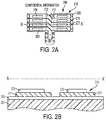
- FIGS. 2A through 2G outline a method of making out of plane coil structures in accordance with some embodiments.
- FIGS. 2A and 2B respectively show top and cross sectional views of a subassembly 200 including a patterned film 210 comprising one or more stress engineered layers 211 disposed on a release layer 205 on a substrate 201 .
- the film 210 can be patterned using standard photolithographic techniques, for example.
- the substrate 201 may comprise glass, silicon, or other suitable substrate materials.
- the release layer 205 may be an electrically conductive material, such as titanium. When a conductive release layer is used, the release layer can be used as a ground plane in an electroplating step.
- the film 210 includes elastic portions 211 having a non-uniform stress profile through the thickness of the one or more layers of the elastic portions 211 such that the elastic portions curl out of plane with respect to the substrate 201 when released from the substrate 201 as shown in FIG. 2B .
- Anchor portions 212 of the film 210 are not released and remain attached to the substrate 201 and attach the elastic portions 211 to the substrate 201.
- the film 210 is stress-engineered, meaning that the film has a stress gradient, or that the stress in the film varies along the thickness of the film, e.g., from the bottom of the film 210 lying on the release layer 205 to the top of the film 210.
- the different stress levels in the film 210 can be introduced in multiple sublayers of the film 210 during sputter deposition of the film material onto the release layer 205.
- the stress levels may be controlled in a variety of ways, including adding a reactive gas to the plasma, depositing the material at an angle, varying the alloy composition of the film material, varying the film material, or changing the pressure of the plasma gas.
- a first layer may be formed of a first material, such as nickel.
- a second layer may be formed from a nickel alloy having slighting different chemical makeup resulting in a different stress characteristic for the second layer.
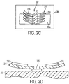
- the film 210 has characteristic that the elastic portions 211 curl up out of the plane of the substrate 201 when released from the release layer 205 as illustrated in FIG. 2C .
- load elements 220 are deposited on the elastic portions 211 to control the curvature of the elastic portions 211 when the elastic portions 211 are released.
- the load elements 220 are additional layers patterned on the elastic portions 211 and that either restrain bending or apply stress that either increases or decreases the bending radius of the elastic portions.
- Each load element 220 can be patterned to reside generally in the middle segment of an elastic portion 211 in some embodiments.
- the load element 220 may made of a reflowable material such as photoresist.
- the load element 220 toughens elastic portions 211 and lengthens the radius of the released elastic portions 211 in comparison to a similar elastic portion without the resist.
- the photoresist can be introduced in the same masking step that creates the release window, or it can be introduced in a separate step.
- the photoresist load element 220 may have very low intrinsic stress when it is processed. Once the elastic portion is released, the photoresist load element 220 is typically on the inside of the bending cantilever, and therefore it accumulates compressive stress upon cantilever release as it opposes the bending.
- One feature of the photoresist load element 220 is that the loading effect of the resist can be gradually changed with either heat or plasma ashing. Heating the 3D structure 200 softens the photoresist load element 220 and causes the photoresist 220 to flow when at temperatures above its glass transition temperature. The width, length, and/or thickness of the load element 220 can be varied in order to adjust the amount of curvature induced in the released elastic portion 211. The load element can be removed after the 3D structure self-assembles.
- Portions of the release layer 205 can be chemically etched in a release window 205a to release the elastic portions 211 which curl away from the substrate 201 as shown in the perspective view of FIG. 2C and the cross sectional diagram of FIG. 2D .
- the subassembly 200 is heated as discussed above, to soften the load layers 220, thereby controlling the curling of the elastic portions 211 during the self-assembly process subsequent to film release.
- FIG. 2E is a cross sectional view depicting self-assembly of the elastic portions 211 after they are released showing the elastic portions 211 in various positions as they are curling away from the substrate.
- FIG. 2F is a photograph showing the self-assembled 3D structure.
- 2G is a photograph that shows the 3D structure after electroplating with Cu. Electroplating with Cu, or other conductive metal, joins the seams where two opposite loops meet, or where the free loop ends meet the anchor portions, making the 3D structure robust and highly electrically conductive.
- the 3D structure can be fabricated using standard wafer-scale processing techniques and may be batch fabricated on integrated circuit wafers as an add on process. Additional details of fabrication processes of 3D structures are described in U.S. Patents 7,713,388 , 7,000,315 , and 6,646, 533 which are incorporated herein by reference.
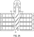
- FIG. 3A illustrates a possible location 395 of the parasitic plating between anchor portions 312-1 and 312-2.
- FIG. 3B is a photograph of a metal bridge 390 formed by parasitic plating.
- FIGS. 4A through 4F show a process sequence illustrating the formation of anchor plating shorts.
- FIG. 4A shows a patterned stress-engineered film 410 comprising elastic portions 411 and anchor portions 412 disposed on an underlying Ti ground plane 405.
- the Ti layer 405 not only functions as a release layer for the elastic portions 411, but also functions as a ground plane that electrically connects all components to be plated.
- a power supply is connected to the ground plane 405, and all components exposed to the plating chemical are batch plated in wafer-scale.
- FIG. 4B shows a release window 430 in photoresist 432 that defines where elastic portions would be released.
- FIG. 4C shows the Ti undercut etch front 431 along the edge of the release window 430 after elastic portions are released (as shown in the photograph of FIG. 2F ).
- FIG. 4D illustrates the elastic portions 411 and the anchor portions 412 after plating which produces parasitic plating 433 around the perimeter of the undercut edge front 431.
- the photoresist 432 is removed (see FIG. 4E ) and all exposed Ti ground plane is etched away.
- FIG. 4F shows the final structure, which incorporates the undesired metal bridge 450 shorting adjacent anchor portions 412..
- the metal bridge 450 can be prevented by covering the exposed edge of the titanium underlayer from plating chemicals.
- One solution to the metal bridge formation involves heating the photoresist 432 to a sufficiently high temperature, causing the photoresist at the undercut edge front 431 to melt and reflow. The intention would be to soften the photoresist so that the softened photoresist would reflow into the undercut region around the Ti undercut edge front 431 and seal the edge 431 against coming into contact with plating chemicals.
- this prior approach is problematic because it is unreliable. This approach is very sensitive to how the photoresist is prepared.
- the photoresist thickness, spin-on process, post-bake temperature, and curing ambient all affect the chance for successful completion of the reflow and sealing process.
- Complete sealing is frequently unsuccessful, and micro-shorts at the anchor regions still form despite effort to seal off the Ti undercut edge.
- Process unreliability leads to low device yields.
- the prior solution significantly limits the microfabrication process tolerance window because a single process step, wafer heating, is used for sealing the ground plane and for softening the load layers to self-assemble the 3D elastic portions. Both functions must be achieved within the parameter space of that process step.
- the wafer must be heated to above 120°C.
- temperatures may be too high for proper 3D assembly of the elastic portions.
- the trajectory of the elastic portions illustrated in FIG. 2E may continue beyond what is shown, the latching mechanism at the tips of the elastic portions would fail, and the elastic portions would not align to properly form 3D loops. In extreme cases, opposite elastic portions would roll into themselves forming pairs of tightly wound individual circular loops.
- the film deposition conditions including ambient pressures and sputter power levels, the film thicknesses, and the mechanical load layer must match the designed stress profile precisely in order for the elastic portions to self-assemble as intended during the photoresist reflow and sealing process. Small drifts in equipment condition and process parameter could cause the coil assembly process to fail.
- the temperature constraints for sealing the Ti undercut edge using reflow of the photoresist significantly limit the available parameter space of film deposition conditions for successful fabrication of the 3D structures.
- Embodiments described herein overcome the issues stated above and provide a reliable way to prevent plating shorts between the anchor regions.
- the disclosed approaches widen the process tolerance for fabricating 3D structures.
- the approaches include patterning the electroplating ground plane to open gaps between adjacent the anchor regions. These openings would then be automatically sealed by photoresist during the subsequent step in the microfabrication process. When designed properly, the sealed openings would prevent metal bridges from forming across the anchor regions during the electroplating process. It also decouples the ground plane sealing process from the coil assembly process, thus significantly widening process tolerance for successful coil fabrication.
- FIGS. 5A through 5F illustrate an approach for reducing or eliminating shorts between anchor portions that develop during electroplating.
- a stress engineered film 510 comprising one or more layers is deposited over a conductive release layer 505 disposed on a substrate.
- the stress engineered film 510 is patterned to include elastic portions 511 and anchor portions 512 as previously discussed.
- the elastic portions 511 curl away from the substrate from the substrate when the release layer is etched beneath them while the anchor portions 512 remain attached to the release layer 505.
- at least one gap 540 is formed in the release layer 505 between neighboring anchor portions 512.
- FIG. 5B shows a release window 530 patterned in a photoresist layer 532 disposed on the release layer 505.
- the release window 530 defines the area where the elastic portions will be released when the release layer is etched.
- a plug of photoresist 532 at least partially fills the gap 540.
- FIG. 5C shows the undercut edge front 531 of the release layer 505 after the portion of the release layer 505 in the release window 530 is etched, releasing the elastic portions 511. As depicted in FIG. 5C , there is now no exposed undercut edge between adjacent anchor portions 512 because that region has been replaced with a photoresist plug.
- the elastic portions 511 and anchor portions 512 are electrically connected by the remaining conductive release layer 505.
- FIG. 5D shows the structure after the electroplating including parasitic plating 533 that forms along the undercut edge front 531.
- the photoresist is stripped ( FIG. 5E ), and all exposed release layer 505 is removed ( FIG. 5F ).
- electroplated stubs 541 are present between anchor portions.
- the stubs 541 extend partially across the distance between the anchor portions but do not electrically connect the adjacent anchor portions 512.
- the stubs are electroplated remnants of the release layer for the elastic portions. As shown in FIG.
- the stubs 541 lie in the x-y plane of the substrate, bending away from the anchor portions 512 along the y-axis, e.g., the stubs 541 bend upward in the orientation shown in FIG. 5F .
- a photoresist artifact is discernable on the substrate between the anchor portions as a faint outline around the release region that shows the shape of the etching undercut below the photoresist mask during device fabrication.
- the photoresist artifact is caused by remaining residues from the release layer 505 after the release layer 505 is removed as in the step shown in FIG. 5F and described above. The residues are embedded into the material below the release layer 505.
- a conductive metal bridge between adjacent anchor portions is prevented in a well-controlled and reliable manner.
- the parasitic plated metal trace 533 around the perimeter of the release window 530 can be similarly eliminated.
- the same method of opening appropriate seal windows release layer can be employed around the anticipated etch front of the undercut.
- the seal window or gap between adjacent springs may be designed so it extends by a distance which is sufficiently deep into the anchor region. Otherwise, the release layer undercut edge 531 could advance beyond the bottom 541 of the gap 540 during the spring release.
- the gaps may extend along the x direction in FIG.
- 5A at least about 50% of a distance between the neighboring anchor portions 512 and/or may extend along the y direction at least about 50% of the length of the anchor portions.
- the distance along the x direction between neighboring anchor portions 512 can less than about 100 ⁇ m in some embodiments.
- On-chip out-of-plane coil structures produced in accordance with the invention have numerous practical applications. For example, when produced with inductance values in the range of 1 to 100 nH, the out-of-plane inductor coil structures are optimally suited for use in mobile RF communication devices that operate in a frequency range of approximately 100 MHz to several GHz. In addition to their use as inductors, the out-of-plane coils can also be used as transformers. Micro-transformers are used in electronic components such as mixers, double-tuned filters and RF signal transformers. The out-of-plane coils are compatible with a variety of micro-transformer architectures.
- Out-of-plane structures made in accordance with the embodiments disclosed herein may be used in any circuit formed on a substrate.
- FIG. 6A provides a cross sectional diagram a circuit system 600A in accordance with some embodiments.
- the circuit system 600A includes one or more electronic components 650 disposed on the circuit substrate 601.
- An electrically conductive three dimensional structure e.g., a 3D coil, is electrically coupled to at least one of the electronic components 650.
- the three dimensional 1 structure 610 includes a film comprising one or more stress engineered layers that include elastic portions 611 having a non-uniform stress profile through the thickness of the one or more layers such that the elastic portions 611 are curled into a three dimensional shape.
- Anchor portions 612 attach the elastic portions 611 to the circuit substrate 601.
- An outer conductive layer is disposed, e.g., by electroplating, over the elastic portions 611 and the anchor portions 612.
- One or more conductive stubs (shown in FIG. 5F ) extend between two adjacent anchor portions 612 without electrically connecting the two adjacent anchor portions 612. Electrical connections between the 3D structure and electronic component 650 may be made by conductive traces disposed on the surface of and/or within the circuit substrate 601.
- FIG. 6B shows another embodiment of a circuit system 600B that includes a 3D structure 620 electrically coupled to electronic components 650.
- the circuit system 600B includes additional interlayers 661, 662 and conductive routing structures 671, 672, 673, 674, 675 that may be used for interconnecting the 3D structure 620 and electronic components 650.
- the interlayers 661, 662 are dielectric layers disposed between the three dimensional structure 620 and the circuit substrate 601.
- Interlayer 661 is disposed on the substrate 601 and may comprise a dielectric such as SiO2, SiON, SiN, for example.
- Interlayer 662 may comprise a low loss tangent material such as benzocyclobutene (BCB).
- BCB benzocyclobutene
- Routing trace metal layers 673, 674 are disposed between the interlayers 671 and 672. Routing trace metal layer 675 is disposed on the circuit substrate.
- the trace metal layers 673, 674, 675 can comprises multiple sublayers, e.g., evaporated and/or plated metal sections.
- Vias 612 connect the 3D coil 620 to the routing traces 673, 674. Routing trace 675 is connected to the electronic component 650. Via 671 interconnects the routing trace 675 routing traces 673, 674.
Landscapes
- Engineering & Computer Science (AREA)
- Power Engineering (AREA)
- Microelectronics & Electronic Packaging (AREA)
- Manufacturing & Machinery (AREA)
- Coils Or Transformers For Communication (AREA)
- Micromachines (AREA)
- Internal Circuitry In Semiconductor Integrated Circuit Devices (AREA)
- Semiconductor Integrated Circuits (AREA)
Abstract
Description
- This disclosure relates generally to electrical micro-device structures and to methods for making such structures.
- Out-of-plane structures, such as three dimensional coils, offer several advantages over in-plane structures. Out-of-plane coils place the coil axis parallel, rather than perpendicular, to the substrate plane. Additionally, out-of-plane coils reduce eddy currents induced in the underlying substrate, and when out-of-plane coils are operated at high frequencies, allow for better control of skin and proximity effects.
- Some embodiments are directed to a method for forming a three dimensional structure. A stress engineered film is deposited over a conductive layer. The stress engineered film includes elastic portions having a non-uniform stress profile through the thickness of the one or more layers such that the stress engineered film curls when released from the conductive layer. The stress engineered film also includes anchor portions that remain attached to the conductive layer. Gaps are formed in the conductive layer between neighboring anchor portions. A mask layer that defines one or more release windows is deposited. The conductive layer is etched in the release windows. The etching of the conductive layer releases the elastic portions of the stress engineered film such that the elastic portions curl to form the three dimensional structure. The three dimensional structure is electroplated using the conductive layer as a contact for the electroplating.
- Some embodiments involve a three dimensional device. The device includes a substrate and a film comprising one or more stress engineered layers. The film includes elastic portions that are curled out of plane with respect to the substrate and anchor portions that attach the elastic portions and to the substrate. An outer conductive layer is disposed over the elastic portions and the anchor portions. The device includes one or more electrically conductive stubs that extend between two adjacent anchor portions without electrically connecting the two adjacent anchor portions.
- In accordance with some embodiments, a circuit system includes a circuit substrate and one or more electronic components. The system further includes an electrically conductive three dimensional structure electrically connected to at least one of the electronic components. The three dimensional structure comprises a film comprising one or more stress engineered layers. The film has elastic portions curled into a three dimensional shape and anchor portions that attach the elastic portions and to substrate. An outer conductive layer is disposed over the elastic portions and the anchor portions. One or more conductive stubs extend between two adjacent anchor portions without electrically connecting the two adjacent anchor portions.
- These and other aspects of the present application will be apparent from the detailed description below. In no event, however, should the above summaries be construed as limitations on the claimed subject matter, which subject matter is defined solely by the attached claims.
-
-
FIG. 1 is a scanning electron micrograph showing perspective view of a coil structure comprising a micro fabricated on-chip 3D coil inductor in accordance with some embodiments; -
FIGS. 2A through 2G outline a method of making out of plane coil structures in accordance with some embodiments; -
FIG. 3A illustrates a possible location of parasitic plating between anchor portions; -
FIG. 3B is a micrograph of a metal bridge formed by parasitic plating; -
FIGS. 4A through 4F show a process sequence illustrating the formation of anchor plating shorts; -
FIGS. 5A through 5F illustrate an approach for reducing or eliminating shorts between anchor portions that develop during electroplating in accordance with some embodiments; and -
FIGS. 6A and 6B provide cross sectional diagrams of circuit systems in accordance with some embodiments. - The figures are not necessarily to scale. Like numbers used in the figures refer to like components. However, it will be understood that the use of a number to refer to a component in a given figure is not intended to limit the component in another figure labeled with the same number.
- Embodiments described herein are directed to out-of-plane structures and methods for making out of plane structures. In some embodiments the out-of-plane structures are coil structures comprising coil windings that self-assemble. The coil windings comprise electrically conductive elastic members that have an intrinsic stress profile. Coil windings are made by introducing an intrinsic stress profile of a certain amount into the elastic members that is designed to produce the desired coil winding height and curvature. A reproducible built-in stress gradient or intrinsic stress profile can be designed into a thin film by varying the growth conditions appropriately during deposition to produce coil windings, e.g., a released elastic member which bends back on itself producing a full or half coil winding. When released from the substrate, the elastic members curl to form out of plane coil windings due to their intrinsic stress profile. Optionally the curling can be controlled by load elements disposed on the elastic members. The electrically conductive coil windings may optionally be held in a spaced apart configuration by non-electrically conductive tethers that connect the coil windings. After the coil structures are self-formed in the manner described above, the coil structures are electroplated for electrical connection and/or to increase the electrical conductivity of the coil windings. The approaches described in this disclosure allow for fabrication of an out of plane, high Q factor micro-coil structure with Q factor greater than about 10 and adjacent coil windings that are separated by less than about 100 um. During operation, the three dimensional (3D) out-of-plane coil windings orient the magnetic field parallel to the substrate surface, resulting in low energy loss and high quality-factor performance.
- The methods and structures disclosed herein employ some of the techniques disclosed in
US Patents 7,713,388 ,7,000,315 ,6,856,225 ,6,646,533 ,6,392,524 ,5,613,861 ,5,848,685 , and5,914,218 which are all incorporated herein by reference. Coils or springs are made by introducing an intrinsic stress profile of a certain amount designed to provide the desired coil winding or spring height and/or curvature. A reproducible built-in stress profile can be designed into a thin film by varying the growth conditions appropriately during deposition to produce coil structures that are "self-assembling." Self-assembling coil structures include released elastic members which bend back on themselves producing coil windings. By using or adding one or more conductive layers, a coil structure suitable for use as an inductor or transformer may be manufactured. -
FIG. 1 is a scanning electron micrograph showing a perspective view of acoil structure 100 comprising a microfabricated on-chip3D coil inductor 102. Thecoil structure 100 comprises asubstrate 101 and acoil 102 disposed on thesubstrate 101. Each coil winding 110 comprises an electrically conductive elastic material, that, as deposited, has an intrinsic stress profile which biases a free end of the coil winding 110 away from thesubstrate 101. The intrinsic stress at the free end relaxes as that released section of the elastic material curls away from the substrate. Each coil winding 110 is electrically connected to thesubstrate 101 by arespective anchor portion 115. The electroplatedcoil windings 110 are electrically connected together through theanchor portions 115. In some embodiments, the distance between thecoil windings 110 is less than about 100 µm. In some embodiments, a ratio between a width of thecoil windings 110 and the distance between thecoil windings 110 is greater than about 2. - The
coil structure 100 may be fabricated using standard wafer-scale processing techniques, and can be batch-fabricated on integrated circuit wafers as an add-on process. Thecoil 102 may be fabricated by depositing and subsequently releasing patterned stress-engineered thin films from thesubstrate 101. The released portions of the film curl up from opposite ends and self-assemble in air to formcoil windings 110. The resulting three dimensional (3D) structure forms a scaffold that is then electroplated with highly conductive metal, such as Cu. In the example ofFIG. 1 , the plating process joins theseams 110a where two opposite coil windings meet. It also patches perforations on the coil windings employed for facilitating film release from the substrate. The plated metal makes the3D structure 100 robust, and makes the coil highly electrically conductive. -
FIGS. 2A through 2G outline a method of making out of plane coil structures in accordance with some embodiments.FIGS. 2A and 2B respectively show top and cross sectional views of asubassembly 200 including a patternedfilm 210 comprising one or more stress engineeredlayers 211 disposed on arelease layer 205 on asubstrate 201 . Thefilm 210 can be patterned using standard photolithographic techniques, for example. Thesubstrate 201 may comprise glass, silicon, or other suitable substrate materials. Therelease layer 205 may be an electrically conductive material, such as titanium. When a conductive release layer is used, the release layer can be used as a ground plane in an electroplating step. - The
film 210 includeselastic portions 211 having a non-uniform stress profile through the thickness of the one or more layers of theelastic portions 211 such that the elastic portions curl out of plane with respect to thesubstrate 201 when released from thesubstrate 201 as shown inFIG. 2B .Anchor portions 212 of thefilm 210 are not released and remain attached to thesubstrate 201 and attach theelastic portions 211 to thesubstrate 201. - The
film 210 is stress-engineered, meaning that the film has a stress gradient, or that the stress in the film varies along the thickness of the film, e.g., from the bottom of thefilm 210 lying on therelease layer 205 to the top of thefilm 210. The different stress levels in thefilm 210 can be introduced in multiple sublayers of thefilm 210 during sputter deposition of the film material onto therelease layer 205. The stress levels may be controlled in a variety of ways, including adding a reactive gas to the plasma, depositing the material at an angle, varying the alloy composition of the film material, varying the film material, or changing the pressure of the plasma gas. Another approach to create a stress gradient in the film would be to form therelease layer 205 out of a conductive material and use it as an electrode in electroplating different layers having different stress properties to form the film. For example, a first layer may be formed of a first material, such as nickel. A second layer may be formed from a nickel alloy having slighting different chemical makeup resulting in a different stress characteristic for the second layer. Regardless of how thefilm 210 is formed, thefilm 210 has characteristic that theelastic portions 211 curl up out of the plane of thesubstrate 201 when released from therelease layer 205 as illustrated inFIG. 2C . - According to some embodiments,
load elements 220 are deposited on theelastic portions 211 to control the curvature of theelastic portions 211 when theelastic portions 211 are released. Theload elements 220 are additional layers patterned on theelastic portions 211 and that either restrain bending or apply stress that either increases or decreases the bending radius of the elastic portions. Eachload element 220 can be patterned to reside generally in the middle segment of anelastic portion 211 in some embodiments. - The
load element 220 may made of a reflowable material such as photoresist. Theload element 220 toughenselastic portions 211 and lengthens the radius of the releasedelastic portions 211 in comparison to a similar elastic portion without the resist. The photoresist can be introduced in the same masking step that creates the release window, or it can be introduced in a separate step. Thephotoresist load element 220 may have very low intrinsic stress when it is processed. Once the elastic portion is released, thephotoresist load element 220 is typically on the inside of the bending cantilever, and therefore it accumulates compressive stress upon cantilever release as it opposes the bending. One feature of thephotoresist load element 220 is that the loading effect of the resist can be gradually changed with either heat or plasma ashing. Heating the3D structure 200 softens thephotoresist load element 220 and causes thephotoresist 220 to flow when at temperatures above its glass transition temperature. The width, length, and/or thickness of theload element 220 can be varied in order to adjust the amount of curvature induced in the releasedelastic portion 211. The load element can be removed after the 3D structure self-assembles. - Portions of the
release layer 205 can be chemically etched in arelease window 205a to release theelastic portions 211 which curl away from thesubstrate 201 as shown in the perspective view ofFIG. 2C and the cross sectional diagram ofFIG. 2D . Thesubassembly 200 is heated as discussed above, to soften the load layers 220, thereby controlling the curling of theelastic portions 211 during the self-assembly process subsequent to film release.FIG. 2E is a cross sectional view depicting self-assembly of theelastic portions 211 after they are released showing theelastic portions 211 in various positions as they are curling away from the substrate.FIG. 2F is a photograph showing the self-assembled 3D structure.FIG. 2G is a photograph that shows the 3D structure after electroplating with Cu. Electroplating with Cu, or other conductive metal, joins the seams where two opposite loops meet, or where the free loop ends meet the anchor portions, making the 3D structure robust and highly electrically conductive. The 3D structure can be fabricated using standard wafer-scale processing techniques and may be batch fabricated on integrated circuit wafers as an add on process. Additional details of fabrication processes of 3D structures are described inU.S. Patents 7,713,388 ,7,000,315 , and6,646, 533 which are incorporated herein by reference. - An issue that can arise during the electroplating process is that unintended metal develops on the substrate between the anchor portions, e.g., near the takeoff locations of the elastic portions. The parasitic plating at the anchor portions can bridge across the space between two neighboring anchor portions causing an electrically short between adjacent coil windings.
FIG. 3A illustrates apossible location 395 of the parasitic plating between anchor portions 312-1 and 312-2.FIG. 3B is a photograph of ametal bridge 390 formed by parasitic plating. - Approaches described herein reduce or prevent parasitic plating shorts between anchor regions and widen the processing tolerance for 3D structures. Generally, the metal bridging issue is caused by incomplete sealing of the underlying ground plane from electroplating chemicals during the plating process.
FIGS. 4A through 4F show a process sequence illustrating the formation of anchor plating shorts.FIG. 4A shows a patterned stress-engineeredfilm 410 comprisingelastic portions 411 andanchor portions 412 disposed on an underlyingTi ground plane 405. TheTi layer 405 not only functions as a release layer for theelastic portions 411, but also functions as a ground plane that electrically connects all components to be plated. During the plating step, a power supply is connected to theground plane 405, and all components exposed to the plating chemical are batch plated in wafer-scale. -
FIG. 4B shows arelease window 430 inphotoresist 432 that defines where elastic portions would be released.FIG. 4C shows the Ti undercutetch front 431 along the edge of therelease window 430 after elastic portions are released (as shown in the photograph ofFIG. 2F ). - During the electroplating process, metal can form around the perimeter of the undercut
etch front 431 because the edge of theTi underlayer 405 is electrically conducting and exposed to plating chemicals.FIG. 4D illustrates theelastic portions 411 and theanchor portions 412 after plating which producesparasitic plating 433 around the perimeter of the undercutedge front 431. After the plating step, thephotoresist 432 is removed (seeFIG. 4E ) and all exposed Ti ground plane is etched away.FIG. 4F shows the final structure, which incorporates the undesired metal bridge 450 shortingadjacent anchor portions 412.. - The metal bridge 450 can be prevented by covering the exposed edge of the titanium underlayer from plating chemicals. One solution to the metal bridge formation involves heating the
photoresist 432 to a sufficiently high temperature, causing the photoresist at the undercutedge front 431 to melt and reflow. The intention would be to soften the photoresist so that the softened photoresist would reflow into the undercut region around the Ti undercutedge front 431 and seal theedge 431 against coming into contact with plating chemicals. However this prior approach is problematic because it is unreliable. This approach is very sensitive to how the photoresist is prepared. For example, the photoresist thickness, spin-on process, post-bake temperature, and curing ambient (vacuum or hot plate) all affect the chance for successful completion of the reflow and sealing process. Complete sealing is frequently unsuccessful, and micro-shorts at the anchor regions still form despite effort to seal off the Ti undercut edge. Process unreliability leads to low device yields. Additionally, the prior solution significantly limits the microfabrication process tolerance window because a single process step, wafer heating, is used for sealing the ground plane and for softening the load layers to self-assemble the 3D elastic portions. Both functions must be achieved within the parameter space of that process step. - For example, to achieve sufficient reflow for sealing the Ti undercut edge, the wafer must be heated to above 120°C. However, for a given stress-engineered film stress profile and thickness, such temperatures may be too high for proper 3D assembly of the elastic portions. Upon heating, the trajectory of the elastic portions illustrated in
FIG. 2E may continue beyond what is shown, the latching mechanism at the tips of the elastic portions would fail, and the elastic portions would not align to properly form 3D loops. In extreme cases, opposite elastic portions would roll into themselves forming pairs of tightly wound individual circular loops. In this scenario, the film deposition conditions, including ambient pressures and sputter power levels, the film thicknesses, and the mechanical load layer must match the designed stress profile precisely in order for the elastic portions to self-assemble as intended during the photoresist reflow and sealing process. Small drifts in equipment condition and process parameter could cause the coil assembly process to fail. Hence, the temperature constraints for sealing the Ti undercut edge using reflow of the photoresist significantly limit the available parameter space of film deposition conditions for successful fabrication of the 3D structures. - Embodiments described herein overcome the issues stated above and provide a reliable way to prevent plating shorts between the anchor regions. The disclosed approaches widen the process tolerance for fabricating 3D structures. According to some embodiments, the approaches include patterning the electroplating ground plane to open gaps between adjacent the anchor regions. These openings would then be automatically sealed by photoresist during the subsequent step in the microfabrication process. When designed properly, the sealed openings would prevent metal bridges from forming across the anchor regions during the electroplating process. It also decouples the ground plane sealing process from the coil assembly process, thus significantly widening process tolerance for successful coil fabrication.
-
FIGS. 5A through 5F illustrate an approach for reducing or eliminating shorts between anchor portions that develop during electroplating. As illustrated inFIG. 5A , a stress engineeredfilm 510 comprising one or more layers is deposited over aconductive release layer 505 disposed on a substrate. The stress engineeredfilm 510 is patterned to includeelastic portions 511 andanchor portions 512 as previously discussed. Theelastic portions 511 curl away from the substrate from the substrate when the release layer is etched beneath them while theanchor portions 512 remain attached to therelease layer 505. As illustrated inFIG. 5A , at least onegap 540 is formed in therelease layer 505 between neighboringanchor portions 512. -
FIG. 5B shows arelease window 530 patterned in aphotoresist layer 532 disposed on therelease layer 505. Therelease window 530 defines the area where the elastic portions will be released when the release layer is etched. A plug ofphotoresist 532 at least partially fills thegap 540.FIG. 5C shows the undercutedge front 531 of therelease layer 505 after the portion of therelease layer 505 in therelease window 530 is etched, releasing theelastic portions 511. As depicted inFIG. 5C , there is now no exposed undercut edge betweenadjacent anchor portions 512 because that region has been replaced with a photoresist plug. Theelastic portions 511 andanchor portions 512 are electrically connected by the remainingconductive release layer 505. Electroplating is performed using the release layer as the electroplating ground connection.FIG. 5D shows the structure after the electroplating includingparasitic plating 533 that forms along the undercutedge front 531. After electroplating, the photoresist is stripped (FIG. 5E ), and all exposedrelease layer 505 is removed (FIG. 5F ). As illustrated inFIG. 5F , electroplatedstubs 541 are present between anchor portions. Thestubs 541 extend partially across the distance between the anchor portions but do not electrically connect theadjacent anchor portions 512. The stubs are electroplated remnants of the release layer for the elastic portions. As shown inFIG. 5F , thestubs 541 lie in the x-y plane of the substrate, bending away from theanchor portions 512 along the y-axis, e.g., thestubs 541 bend upward in the orientation shown inFIG. 5F . In some scenarios, a photoresist artifact is discernable on the substrate between the anchor portions as a faint outline around the release region that shows the shape of the etching undercut below the photoresist mask during device fabrication. The photoresist artifact is caused by remaining residues from therelease layer 505 after therelease layer 505 is removed as in the step shown inFIG. 5F and described above. The residues are embedded into the material below therelease layer 505. - According to the process outlined in
FIGS. 5A through 5F , a conductive metal bridge between adjacent anchor portions is prevented in a well-controlled and reliable manner. If desired, the parasitic platedmetal trace 533 around the perimeter of therelease window 530 can be similarly eliminated. The same method of opening appropriate seal windows release layer can be employed around the anticipated etch front of the undercut. The seal window or gap between adjacent springs may be designed so it extends by a distance which is sufficiently deep into the anchor region. Otherwise, the release layer undercutedge 531 could advance beyond thebottom 541 of thegap 540 during the spring release. For example, the gaps may extend along the x direction inFIG. 5A at least about 50% of a distance between the neighboringanchor portions 512 and/or may extend along the y direction at least about 50% of the length of the anchor portions. The distance along the x direction between neighboringanchor portions 512 can less than about 100 µm in some embodiments. - On-chip out-of-plane coil structures produced in accordance with the invention have numerous practical applications. For example, when produced with inductance values in the range of 1 to 100 nH, the out-of-plane inductor coil structures are optimally suited for use in mobile RF communication devices that operate in a frequency range of approximately 100 MHz to several GHz. In addition to their use as inductors, the out-of-plane coils can also be used as transformers. Micro-transformers are used in electronic components such as mixers, double-tuned filters and RF signal transformers. The out-of-plane coils are compatible with a variety of micro-transformer architectures. Examples of micro-transformer designs using the out-of-plane coils are described in the
US Patents 6,856,225 and6,392,524 which are incorporated herein by reference. Out-of-plane structures made in accordance with the embodiments disclosed herein may be used in any circuit formed on a substrate. -
FIG. 6A provides a cross sectional diagram acircuit system 600A in accordance with some embodiments. Thecircuit system 600A includes one or moreelectronic components 650 disposed on thecircuit substrate 601. An electrically conductive three dimensional structure, e.g., a 3D coil, is electrically coupled to at least one of theelectronic components 650. The three dimensional 1structure 610 includes a film comprising one or more stress engineered layers that includeelastic portions 611 having a non-uniform stress profile through the thickness of the one or more layers such that theelastic portions 611 are curled into a three dimensional shape.Anchor portions 612 attach theelastic portions 611 to thecircuit substrate 601. An outer conductive layer is disposed, e.g., by electroplating, over theelastic portions 611 and theanchor portions 612. One or more conductive stubs (shown inFIG. 5F ) extend between twoadjacent anchor portions 612 without electrically connecting the twoadjacent anchor portions 612. Electrical connections between the 3D structure andelectronic component 650 may be made by conductive traces disposed on the surface of and/or within thecircuit substrate 601. -
FIG. 6B shows another embodiment of acircuit system 600B that includes a3D structure 620 electrically coupled toelectronic components 650. Thecircuit system 600B includesadditional interlayers conductive routing structures 3D structure 620 andelectronic components 650. Theinterlayers dimensional structure 620 and thecircuit substrate 601.Interlayer 661 is disposed on thesubstrate 601 and may comprise a dielectric such as SiO2, SiON, SiN, for example.Interlayer 662 may comprise a low loss tangent material such as benzocyclobutene (BCB). - Routing
trace metal layers interlayers trace metal layer 675 is disposed on the circuit substrate. Thetrace metal layers Vias 612 connect the3D coil 620 to the routing traces 673, 674.Routing trace 675 is connected to theelectronic component 650. Via 671 interconnects therouting trace 675 routing traces 673, 674. - Unless otherwise indicated, all numbers expressing feature sizes, amounts, and physical properties used in the specification and claims are to be understood as being modified in all instances by the term "about." Accordingly, unless indicated to the contrary, the numerical parameters set forth in the foregoing specification and attached claims are approximations that can vary depending upon the desired properties sought to be obtained by those skilled in the art utilizing the teachings disclosed herein. The use of numerical ranges by endpoints includes all numbers within that range (e.g. 1 to 5 includes 1, 1.5, 2, 2.75, 3, 3.80, 4, and 5) and any range within that range.
- Various modifications and alterations of the embodiments discussed above will be apparent to those skilled in the art, and it should be understood that this disclosure is not limited to the illustrative embodiments set forth herein. The reader should assume that features of one disclosed embodiment can also be applied to all other disclosed embodiments unless otherwise indicated. It should also be understood that all U.S. patents, patent applications, patent application publications, and other patent and non-patent documents referred to herein are incorporated by reference, to the extent they do not contradict the foregoing disclosure.
Claims (10)
- A method for forming a three dimensional structure comprising:depositing a stress engineered film over a conductive layer, the stress engineered film including:elastic portions having a non-uniform stress profile through the thickness of the one or more layers such that the stress engineered film curls when released from the conductive layer; andanchor portions configured to remain attached to the conductive layer;forming gaps in the conductive layer between neighboring anchor portions;depositing a mask layer defining one or more release windows;etching the conductive layer in the release windows, the etching releasing the elastic portions of the stress engineered film such that the elastic portions curl to form the three dimensional structure; andelectroplating the three dimensional structure using the conductive layer as a contact for the electroplating.
- The method of claim 1, wherein depositing the mask layer comprises depositing mask material within the gaps.
- The method of claim 1, wherein the elastic portions of the stress engineered film curl to form three dimensional coil loops.
- The method of claim 1, wherein the gaps extend at least 50% of a distance between the neighboring anchor portions.
- The method of claim 1, wherein the gaps extend at least 50% of a length of the anchor portions.
- The method of claim 1, wherein a distance between neighboring anchor portions is less than about 100 µm.
- A device comprising:a substrate;a film comprising one or more stress engineered layers, the film comprising:elastic portions that are curled out of plane with respect to the substrate; andanchor portions that attach the elastic portions and to the substrate;an outer conductive layer disposed over the elastic portions and the anchor portions; andone or more electrically conductive stubs that extend between two adjacent anchor portions without electrically connecting the two adjacent anchor portions.
- The device of claim 7, further comprising a photoresist artifact disposed on the substrate between the anchor portions.
- A circuit system comprising:a circuit substrate;one or more electronic components disposed on the circuit substrate;an electrically conductive three dimensional structure electrically connected to at least one of the electronic components, the three dimensional structure comprising:one or more conductive stubs that extend between two adjacent anchor portions without electrically connecting the two adjacent anchor portions.a film comprising one or more stress engineered layers, the film comprising:elastic portions curled into a three dimensional shape; andanchor portions attached to the elastic portions; andan outer conductive layer disposed over the elastic portions and the anchor portions; and
- The system of claim 9, further comprising one or more dielectric interlayers disposed between the three dimensional structure and the circuit substrate.
Applications Claiming Priority (1)
| Application Number | Priority Date | Filing Date | Title |
|---|---|---|---|
| US15/651,311 US9955575B1 (en) | 2017-07-17 | 2017-07-17 | Out of plane structures and methods for making out of plane structures |
Publications (2)
| Publication Number | Publication Date |
|---|---|
| EP3432324A1 true EP3432324A1 (en) | 2019-01-23 |
| EP3432324B1 EP3432324B1 (en) | 2023-09-06 |
Family
ID=61951824
Family Applications (1)
| Application Number | Title | Priority Date | Filing Date |
|---|---|---|---|
| EP18181301.5A Active EP3432324B1 (en) | 2017-07-17 | 2018-07-02 | Out of plane structures and methods for making out of plane structures |
Country Status (3)
| Country | Link |
|---|---|
| US (1) | US9955575B1 (en) |
| EP (1) | EP3432324B1 (en) |
| JP (1) | JP6949782B2 (en) |
Cited By (1)
| Publication number | Priority date | Publication date | Assignee | Title |
|---|---|---|---|---|
| CN111508702A (en) * | 2020-06-29 | 2020-08-07 | 广东昭信智能装备有限公司 | Inductance winding machine |
Families Citing this family (3)
| Publication number | Priority date | Publication date | Assignee | Title |
|---|---|---|---|---|
| US11527420B2 (en) | 2021-03-22 | 2022-12-13 | Palo Alto Research Center Incorporated | Micro-fabricated, stress-engineered members formed on passivation layer of integrated circuit |
| US11908782B2 (en) | 2021-03-22 | 2024-02-20 | Xerox Corporation | Spacers formed on a substrate with etched micro-springs |
| US12224082B2 (en) | 2023-02-09 | 2025-02-11 | Xerox Corporation | Stress engineered microspring for cryogenic superconducting circuits |
Citations (8)
| Publication number | Priority date | Publication date | Assignee | Title |
|---|---|---|---|---|
| US5613861A (en) | 1995-06-07 | 1997-03-25 | Xerox Corporation | Photolithographically patterned spring contact |
| WO2001088612A1 (en) * | 2000-05-17 | 2001-11-22 | Xerox Corporation | Photolithographically-patterned out-of-plane coil structures and method of making |
| US6392524B1 (en) | 2000-06-09 | 2002-05-21 | Xerox Corporation | Photolithographically-patterned out-of-plane coil structures and method of making |
| US20020173146A1 (en) * | 2001-05-21 | 2002-11-21 | Xerox Corporation | Metal plated spring structure |
| US20050006829A1 (en) * | 2003-07-08 | 2005-01-13 | Xerox Corporation | High force metal plated spring structure |
| US20060030066A1 (en) * | 2004-08-04 | 2006-02-09 | Palo Alto Research Center Incorporated | Intermetallic spring structure |
| US20070148895A1 (en) * | 2005-12-28 | 2007-06-28 | Palo Alto Research Center Incorporated | Integrateable capacitors and microcoils and methods of making thereof |
| US20070202310A1 (en) * | 2006-02-27 | 2007-08-30 | Palo Alto Research Center Incorporated | Out-of plane spring structures on a substrate |
-
2017
- 2017-07-17 US US15/651,311 patent/US9955575B1/en not_active Expired - Fee Related
-
2018
- 2018-06-25 JP JP2018119619A patent/JP6949782B2/en not_active Expired - Fee Related
- 2018-07-02 EP EP18181301.5A patent/EP3432324B1/en active Active
Patent Citations (14)
| Publication number | Priority date | Publication date | Assignee | Title |
|---|---|---|---|---|
| US5613861A (en) | 1995-06-07 | 1997-03-25 | Xerox Corporation | Photolithographically patterned spring contact |
| US5848685A (en) | 1995-06-07 | 1998-12-15 | Xerox Corporation | Photolithographically patterned spring contact |
| US5914218A (en) | 1995-06-07 | 1999-06-22 | Xerox Corporation | Method for forming a spring contact |
| WO2001088612A1 (en) * | 2000-05-17 | 2001-11-22 | Xerox Corporation | Photolithographically-patterned out-of-plane coil structures and method of making |
| US7000315B2 (en) | 2000-05-17 | 2006-02-21 | Xerox Corporation | Method of making photolithographically-patterned out-of-plane coil structures |
| US6856225B1 (en) | 2000-05-17 | 2005-02-15 | Xerox Corporation | Photolithographically-patterned out-of-plane coil structures and method of making |
| US6646533B2 (en) | 2000-06-09 | 2003-11-11 | Xerox Corporation | Photolithographically-patterned out-of-plane coil structures and method of making |
| US6392524B1 (en) | 2000-06-09 | 2002-05-21 | Xerox Corporation | Photolithographically-patterned out-of-plane coil structures and method of making |
| US20020173146A1 (en) * | 2001-05-21 | 2002-11-21 | Xerox Corporation | Metal plated spring structure |
| US20050006829A1 (en) * | 2003-07-08 | 2005-01-13 | Xerox Corporation | High force metal plated spring structure |
| US20060030066A1 (en) * | 2004-08-04 | 2006-02-09 | Palo Alto Research Center Incorporated | Intermetallic spring structure |
| US20070148895A1 (en) * | 2005-12-28 | 2007-06-28 | Palo Alto Research Center Incorporated | Integrateable capacitors and microcoils and methods of making thereof |
| US20070202310A1 (en) * | 2006-02-27 | 2007-08-30 | Palo Alto Research Center Incorporated | Out-of plane spring structures on a substrate |
| US7713388B2 (en) | 2006-02-27 | 2010-05-11 | Palo Alto Research Center Incorporated | Out-of-plane spring structures on a substrate |
Cited By (1)
| Publication number | Priority date | Publication date | Assignee | Title |
|---|---|---|---|---|
| CN111508702A (en) * | 2020-06-29 | 2020-08-07 | 广东昭信智能装备有限公司 | Inductance winding machine |
Also Published As
| Publication number | Publication date |
|---|---|
| JP2019021914A (en) | 2019-02-07 |
| EP3432324B1 (en) | 2023-09-06 |
| JP6949782B2 (en) | 2021-10-13 |
| US9955575B1 (en) | 2018-04-24 |
Similar Documents
| Publication | Publication Date | Title |
|---|---|---|
| EP3432324B1 (en) | Out of plane structures and methods for making out of plane structures | |
| TWI244206B (en) | Photolithographically-patterned variable capacitor structures and method of making | |
| EP1760731B1 (en) | Integrated electronic device | |
| US7517769B2 (en) | Integrateable capacitors and microcoils and methods of making thereof | |
| Yoon et al. | Polymer-core conductor approaches for RF MEMS | |
| US8745853B2 (en) | Antenna fabrication with three-dimensional contoured substrates | |
| EP1231616B1 (en) | Out-of-plane micro-device structures | |
| US7710232B1 (en) | Microelectromechanical tunable inductor | |
| EP1231617B1 (en) | Out-of-plane micro-device structures | |
| JP2003533897A (en) | Three-dimensional coil structure by photolithographic pattern formation and manufacturing method | |
| EP1231182B1 (en) | Method for manufacturing out-of-plane micro-device structures | |
| JP2007158360A (en) | Article with variable inductor | |
| CN100565724C (en) | Variable inductor | |
| CN108305869A (en) | Semiconductor Structure and Method | |
| JP5198777B2 (en) | Method for forming out-of-plane structure on substrate | |
| EP2038901A2 (en) | High inductance, out-of-plane inductors | |
| US7283029B2 (en) | 3-D transformer for high-frequency applications | |
| EP1542261B1 (en) | Method of producing an element comprising an electrical conductor encircled by magnetic material | |
| US6621139B2 (en) | Method for fabricating a tunable, 3-dimensional solenoid and device fabricated | |
| US20070145523A1 (en) | Integrateable capacitors and microcoils and methods of making thereof | |
| US6677659B2 (en) | Method for fabricating 3-dimensional solenoid and device fabricated | |
| CN115411020B (en) | On-chip spiral core inductor, its fabrication method and mass production method | |
| US20090046018A1 (en) | Lithographically controlled curvature for mems devices and antennas | |
| TWI223402B (en) | Whirlpool-like microstructure having spiral conductor layer and manufacturing method thereof | |
| CN110182752B (en) | Method for forming fine structure by electroplating, fine structure and electronic device |
Legal Events
| Date | Code | Title | Description |
|---|---|---|---|
| PUAI | Public reference made under article 153(3) epc to a published international application that has entered the european phase |
Free format text: ORIGINAL CODE: 0009012 |
|
| STAA | Information on the status of an ep patent application or granted ep patent |
Free format text: STATUS: THE APPLICATION HAS BEEN PUBLISHED |
|
| AK | Designated contracting states |
Kind code of ref document: A1 Designated state(s): AL AT BE BG CH CY CZ DE DK EE ES FI FR GB GR HR HU IE IS IT LI LT LU LV MC MK MT NL NO PL PT RO RS SE SI SK SM TR |
|
| AX | Request for extension of the european patent |
Extension state: BA ME |
|
| STAA | Information on the status of an ep patent application or granted ep patent |
Free format text: STATUS: REQUEST FOR EXAMINATION WAS MADE |
|
| 17P | Request for examination filed |
Effective date: 20190723 |
|
| RBV | Designated contracting states (corrected) |
Designated state(s): AL AT BE BG CH CY CZ DE DK EE ES FI FR GB GR HR HU IE IS IT LI LT LU LV MC MK MT NL NO PL PT RO RS SE SI SK SM TR |
|
| STAA | Information on the status of an ep patent application or granted ep patent |
Free format text: STATUS: EXAMINATION IS IN PROGRESS |
|
| 17Q | First examination report despatched |
Effective date: 20200318 |
|
| GRAP | Despatch of communication of intention to grant a patent |
Free format text: ORIGINAL CODE: EPIDOSNIGR1 |
|
| STAA | Information on the status of an ep patent application or granted ep patent |
Free format text: STATUS: GRANT OF PATENT IS INTENDED |
|
| RAP3 | Party data changed (applicant data changed or rights of an application transferred) |
Owner name: PALO ALTO RESEARCH CENTER INCORPORATED |
|
| INTG | Intention to grant announced |
Effective date: 20230307 |
|
| RAP3 | Party data changed (applicant data changed or rights of an application transferred) |
Owner name: PALO ALTO RESEARCH CENTER INCORPORATED |
|
| RAP3 | Party data changed (applicant data changed or rights of an application transferred) |
Owner name: PALO ALTO RESEARCH CENTER INCORPORATED |
|
| GRAS | Grant fee paid |
Free format text: ORIGINAL CODE: EPIDOSNIGR3 |
|
| GRAA | (expected) grant |
Free format text: ORIGINAL CODE: 0009210 |
|
| STAA | Information on the status of an ep patent application or granted ep patent |
Free format text: STATUS: THE PATENT HAS BEEN GRANTED |
|
| AK | Designated contracting states |
Kind code of ref document: B1 Designated state(s): AL AT BE BG CH CY CZ DE DK EE ES FI FR GB GR HR HU IE IS IT LI LT LU LV MC MK MT NL NO PL PT RO RS SE SI SK SM TR |
|
| REG | Reference to a national code |
Ref country code: GB Ref legal event code: FG4D |
|
| REG | Reference to a national code |
Ref country code: CH Ref legal event code: EP |
|
| REG | Reference to a national code |
Ref country code: IE Ref legal event code: FG4D |
|
| REG | Reference to a national code |
Ref country code: DE Ref legal event code: R096 Ref document number: 602018056847 Country of ref document: DE |
|
| REG | Reference to a national code |
Ref country code: LT Ref legal event code: MG9D |
|
| REG | Reference to a national code |
Ref country code: NL Ref legal event code: MP Effective date: 20230906 |
|
| PG25 | Lapsed in a contracting state [announced via postgrant information from national office to epo] |
Ref country code: GR Free format text: LAPSE BECAUSE OF FAILURE TO SUBMIT A TRANSLATION OF THE DESCRIPTION OR TO PAY THE FEE WITHIN THE PRESCRIBED TIME-LIMIT Effective date: 20231207 |
|
| PG25 | Lapsed in a contracting state [announced via postgrant information from national office to epo] |
Ref country code: SE Free format text: LAPSE BECAUSE OF FAILURE TO SUBMIT A TRANSLATION OF THE DESCRIPTION OR TO PAY THE FEE WITHIN THE PRESCRIBED TIME-LIMIT Effective date: 20230906 Ref country code: RS Free format text: LAPSE BECAUSE OF FAILURE TO SUBMIT A TRANSLATION OF THE DESCRIPTION OR TO PAY THE FEE WITHIN THE PRESCRIBED TIME-LIMIT Effective date: 20230906 Ref country code: NO Free format text: LAPSE BECAUSE OF FAILURE TO SUBMIT A TRANSLATION OF THE DESCRIPTION OR TO PAY THE FEE WITHIN THE PRESCRIBED TIME-LIMIT Effective date: 20231206 Ref country code: LV Free format text: LAPSE BECAUSE OF FAILURE TO SUBMIT A TRANSLATION OF THE DESCRIPTION OR TO PAY THE FEE WITHIN THE PRESCRIBED TIME-LIMIT Effective date: 20230906 Ref country code: LT Free format text: LAPSE BECAUSE OF FAILURE TO SUBMIT A TRANSLATION OF THE DESCRIPTION OR TO PAY THE FEE WITHIN THE PRESCRIBED TIME-LIMIT Effective date: 20230906 Ref country code: HR Free format text: LAPSE BECAUSE OF FAILURE TO SUBMIT A TRANSLATION OF THE DESCRIPTION OR TO PAY THE FEE WITHIN THE PRESCRIBED TIME-LIMIT Effective date: 20230906 Ref country code: GR Free format text: LAPSE BECAUSE OF FAILURE TO SUBMIT A TRANSLATION OF THE DESCRIPTION OR TO PAY THE FEE WITHIN THE PRESCRIBED TIME-LIMIT Effective date: 20231207 Ref country code: FI Free format text: LAPSE BECAUSE OF FAILURE TO SUBMIT A TRANSLATION OF THE DESCRIPTION OR TO PAY THE FEE WITHIN THE PRESCRIBED TIME-LIMIT Effective date: 20230906 |
|
| REG | Reference to a national code |
Ref country code: AT Ref legal event code: MK05 Ref document number: 1609676 Country of ref document: AT Kind code of ref document: T Effective date: 20230906 |
|
| PG25 | Lapsed in a contracting state [announced via postgrant information from national office to epo] |
Ref country code: NL Free format text: LAPSE BECAUSE OF FAILURE TO SUBMIT A TRANSLATION OF THE DESCRIPTION OR TO PAY THE FEE WITHIN THE PRESCRIBED TIME-LIMIT Effective date: 20230906 |
|
| PG25 | Lapsed in a contracting state [announced via postgrant information from national office to epo] |
Ref country code: IS Free format text: LAPSE BECAUSE OF FAILURE TO SUBMIT A TRANSLATION OF THE DESCRIPTION OR TO PAY THE FEE WITHIN THE PRESCRIBED TIME-LIMIT Effective date: 20240106 |
|
| PG25 | Lapsed in a contracting state [announced via postgrant information from national office to epo] |
Ref country code: AT Free format text: LAPSE BECAUSE OF FAILURE TO SUBMIT A TRANSLATION OF THE DESCRIPTION OR TO PAY THE FEE WITHIN THE PRESCRIBED TIME-LIMIT Effective date: 20230906 |
|
| PG25 | Lapsed in a contracting state [announced via postgrant information from national office to epo] |
Ref country code: ES Free format text: LAPSE BECAUSE OF FAILURE TO SUBMIT A TRANSLATION OF THE DESCRIPTION OR TO PAY THE FEE WITHIN THE PRESCRIBED TIME-LIMIT Effective date: 20230906 |
|
| PG25 | Lapsed in a contracting state [announced via postgrant information from national office to epo] |
Ref country code: SM Free format text: LAPSE BECAUSE OF FAILURE TO SUBMIT A TRANSLATION OF THE DESCRIPTION OR TO PAY THE FEE WITHIN THE PRESCRIBED TIME-LIMIT Effective date: 20230906 Ref country code: RO Free format text: LAPSE BECAUSE OF FAILURE TO SUBMIT A TRANSLATION OF THE DESCRIPTION OR TO PAY THE FEE WITHIN THE PRESCRIBED TIME-LIMIT Effective date: 20230906 Ref country code: IS Free format text: LAPSE BECAUSE OF FAILURE TO SUBMIT A TRANSLATION OF THE DESCRIPTION OR TO PAY THE FEE WITHIN THE PRESCRIBED TIME-LIMIT Effective date: 20240106 Ref country code: ES Free format text: LAPSE BECAUSE OF FAILURE TO SUBMIT A TRANSLATION OF THE DESCRIPTION OR TO PAY THE FEE WITHIN THE PRESCRIBED TIME-LIMIT Effective date: 20230906 Ref country code: EE Free format text: LAPSE BECAUSE OF FAILURE TO SUBMIT A TRANSLATION OF THE DESCRIPTION OR TO PAY THE FEE WITHIN THE PRESCRIBED TIME-LIMIT Effective date: 20230906 Ref country code: CZ Free format text: LAPSE BECAUSE OF FAILURE TO SUBMIT A TRANSLATION OF THE DESCRIPTION OR TO PAY THE FEE WITHIN THE PRESCRIBED TIME-LIMIT Effective date: 20230906 Ref country code: AT Free format text: LAPSE BECAUSE OF FAILURE TO SUBMIT A TRANSLATION OF THE DESCRIPTION OR TO PAY THE FEE WITHIN THE PRESCRIBED TIME-LIMIT Effective date: 20230906 Ref country code: SK Free format text: LAPSE BECAUSE OF FAILURE TO SUBMIT A TRANSLATION OF THE DESCRIPTION OR TO PAY THE FEE WITHIN THE PRESCRIBED TIME-LIMIT Effective date: 20230906 Ref country code: PT Free format text: LAPSE BECAUSE OF FAILURE TO SUBMIT A TRANSLATION OF THE DESCRIPTION OR TO PAY THE FEE WITHIN THE PRESCRIBED TIME-LIMIT Effective date: 20240108 |
|
| PG25 | Lapsed in a contracting state [announced via postgrant information from national office to epo] |
Ref country code: PL Free format text: LAPSE BECAUSE OF FAILURE TO SUBMIT A TRANSLATION OF THE DESCRIPTION OR TO PAY THE FEE WITHIN THE PRESCRIBED TIME-LIMIT Effective date: 20230906 Ref country code: IT Free format text: LAPSE BECAUSE OF FAILURE TO SUBMIT A TRANSLATION OF THE DESCRIPTION OR TO PAY THE FEE WITHIN THE PRESCRIBED TIME-LIMIT Effective date: 20230906 |
|
| REG | Reference to a national code |
Ref country code: DE Ref legal event code: R097 Ref document number: 602018056847 Country of ref document: DE |
|
| PGFP | Annual fee paid to national office [announced via postgrant information from national office to epo] |
Ref country code: GB Payment date: 20240620 Year of fee payment: 7 |
|
| PG25 | Lapsed in a contracting state [announced via postgrant information from national office to epo] |
Ref country code: DK Free format text: LAPSE BECAUSE OF FAILURE TO SUBMIT A TRANSLATION OF THE DESCRIPTION OR TO PAY THE FEE WITHIN THE PRESCRIBED TIME-LIMIT Effective date: 20230906 |
|
| PLBE | No opposition filed within time limit |
Free format text: ORIGINAL CODE: 0009261 |
|
| STAA | Information on the status of an ep patent application or granted ep patent |
Free format text: STATUS: NO OPPOSITION FILED WITHIN TIME LIMIT |
|
| PG25 | Lapsed in a contracting state [announced via postgrant information from national office to epo] |
Ref country code: DK Free format text: LAPSE BECAUSE OF FAILURE TO SUBMIT A TRANSLATION OF THE DESCRIPTION OR TO PAY THE FEE WITHIN THE PRESCRIBED TIME-LIMIT Effective date: 20230906 Ref country code: SI Free format text: LAPSE BECAUSE OF FAILURE TO SUBMIT A TRANSLATION OF THE DESCRIPTION OR TO PAY THE FEE WITHIN THE PRESCRIBED TIME-LIMIT Effective date: 20230906 |
|
| PGFP | Annual fee paid to national office [announced via postgrant information from national office to epo] |
Ref country code: FR Payment date: 20240619 Year of fee payment: 7 |
|
| 26N | No opposition filed |
Effective date: 20240607 |
|
| PGFP | Annual fee paid to national office [announced via postgrant information from national office to epo] |
Ref country code: DE Payment date: 20240619 Year of fee payment: 7 |
|
| PG25 | Lapsed in a contracting state [announced via postgrant information from national office to epo] |
Ref country code: BG Free format text: LAPSE BECAUSE OF FAILURE TO SUBMIT A TRANSLATION OF THE DESCRIPTION OR TO PAY THE FEE WITHIN THE PRESCRIBED TIME-LIMIT Effective date: 20230906 |
|
| PG25 | Lapsed in a contracting state [announced via postgrant information from national office to epo] |
Ref country code: BG Free format text: LAPSE BECAUSE OF FAILURE TO SUBMIT A TRANSLATION OF THE DESCRIPTION OR TO PAY THE FEE WITHIN THE PRESCRIBED TIME-LIMIT Effective date: 20230906 |
|
| PG25 | Lapsed in a contracting state [announced via postgrant information from national office to epo] |
Ref country code: MC Free format text: LAPSE BECAUSE OF FAILURE TO SUBMIT A TRANSLATION OF THE DESCRIPTION OR TO PAY THE FEE WITHIN THE PRESCRIBED TIME-LIMIT Effective date: 20230906 |
|
| REG | Reference to a national code |
Ref country code: CH Ref legal event code: PL |
|
| PG25 | Lapsed in a contracting state [announced via postgrant information from national office to epo] |
Ref country code: LU Free format text: LAPSE BECAUSE OF NON-PAYMENT OF DUE FEES Effective date: 20240702 |
|
| PG25 | Lapsed in a contracting state [announced via postgrant information from national office to epo] |
Ref country code: LU Free format text: LAPSE BECAUSE OF NON-PAYMENT OF DUE FEES Effective date: 20240702 |
|
| PG25 | Lapsed in a contracting state [announced via postgrant information from national office to epo] |
Ref country code: CH Free format text: LAPSE BECAUSE OF NON-PAYMENT OF DUE FEES Effective date: 20240731 Ref country code: BE Free format text: LAPSE BECAUSE OF NON-PAYMENT OF DUE FEES Effective date: 20240731 |
|
| REG | Reference to a national code |
Ref country code: BE Ref legal event code: MM Effective date: 20240731 |
|
| PG25 | Lapsed in a contracting state [announced via postgrant information from national office to epo] |
Ref country code: IE Free format text: LAPSE BECAUSE OF NON-PAYMENT OF DUE FEES Effective date: 20240702 |
|
| PG25 | Lapsed in a contracting state [announced via postgrant information from national office to epo] |
Ref country code: CY Free format text: LAPSE BECAUSE OF FAILURE TO SUBMIT A TRANSLATION OF THE DESCRIPTION OR TO PAY THE FEE WITHIN THE PRESCRIBED TIME-LIMIT; INVALID AB INITIO Effective date: 20180702 |
|
| REG | Reference to a national code |
Ref country code: DE Ref legal event code: R119 Ref document number: 602018056847 Country of ref document: DE |
|
| PG25 | Lapsed in a contracting state [announced via postgrant information from national office to epo] |
Ref country code: HU Free format text: LAPSE BECAUSE OF FAILURE TO SUBMIT A TRANSLATION OF THE DESCRIPTION OR TO PAY THE FEE WITHIN THE PRESCRIBED TIME-LIMIT; INVALID AB INITIO Effective date: 20180702 |
|
| GBPC | Gb: european patent ceased through non-payment of renewal fee |
Effective date: 20250702 |
|
| PG25 | Lapsed in a contracting state [announced via postgrant information from national office to epo] |
Ref country code: GB Free format text: LAPSE BECAUSE OF NON-PAYMENT OF DUE FEES Effective date: 20250702 |
|
| PG25 | Lapsed in a contracting state [announced via postgrant information from national office to epo] |
Ref country code: DE Free format text: LAPSE BECAUSE OF NON-PAYMENT OF DUE FEES Effective date: 20260203 |
|
| PG25 | Lapsed in a contracting state [announced via postgrant information from national office to epo] |
Ref country code: FR Free format text: LAPSE BECAUSE OF NON-PAYMENT OF DUE FEES Effective date: 20250731 |
|
| PG25 | Lapsed in a contracting state [announced via postgrant information from national office to epo] |
Ref country code: TR Free format text: LAPSE BECAUSE OF FAILURE TO SUBMIT A TRANSLATION OF THE DESCRIPTION OR TO PAY THE FEE WITHIN THE PRESCRIBED TIME-LIMIT Effective date: 20230906 |