EP3432190B1 - Processing system and related integrated circuit for handling password management - Google Patents
Processing system and related integrated circuit for handling password management Download PDFInfo
- Publication number
- EP3432190B1 EP3432190B1 EP18182223.0A EP18182223A EP3432190B1 EP 3432190 B1 EP3432190 B1 EP 3432190B1 EP 18182223 A EP18182223 A EP 18182223A EP 3432190 B1 EP3432190 B1 EP 3432190B1
- Authority
- EP
- European Patent Office
- Prior art keywords
- password
- configuration data
- processing system
- circuit
- volatile memory
- Prior art date
- Legal status (The legal status is an assumption and is not a legal conclusion. Google has not performed a legal analysis and makes no representation as to the accuracy of the status listed.)
- Active
Links
- 238000012545 processing Methods 0.000 title claims description 164
- 230000015654 memory Effects 0.000 claims description 105
- 230000004224 protection Effects 0.000 claims description 98
- 238000012795 verification Methods 0.000 claims description 98
- 238000004891 communication Methods 0.000 claims description 28
- 230000006870 function Effects 0.000 claims description 18
- 238000012360 testing method Methods 0.000 claims description 9
- 230000004044 response Effects 0.000 claims description 6
- 230000008859 change Effects 0.000 claims description 3
- 230000006399 behavior Effects 0.000 description 5
- 238000004519 manufacturing process Methods 0.000 description 4
- 230000007246 mechanism Effects 0.000 description 4
- 102100022404 E3 ubiquitin-protein ligase Midline-1 Human genes 0.000 description 3
- 101000680670 Homo sapiens E3 ubiquitin-protein ligase Midline-1 Proteins 0.000 description 3
- 230000001276 controlling effect Effects 0.000 description 2
- 238000000034 method Methods 0.000 description 2
- 230000001105 regulatory effect Effects 0.000 description 2
- 230000009471 action Effects 0.000 description 1
- 238000004458 analytical method Methods 0.000 description 1
- 230000005540 biological transmission Effects 0.000 description 1
- 238000004364 calculation method Methods 0.000 description 1
- 238000010276 construction Methods 0.000 description 1
- 230000001419 dependent effect Effects 0.000 description 1
- 238000013461 design Methods 0.000 description 1
- 238000010586 diagram Methods 0.000 description 1
- 230000008520 organization Effects 0.000 description 1
- 230000002093 peripheral effect Effects 0.000 description 1
- 230000036316 preload Effects 0.000 description 1
- 230000008569 process Effects 0.000 description 1
- 238000012546 transfer Methods 0.000 description 1
Images


Classifications
-
- G—PHYSICS
- G06—COMPUTING; CALCULATING OR COUNTING
- G06F—ELECTRIC DIGITAL DATA PROCESSING
- G06F21/00—Security arrangements for protecting computers, components thereof, programs or data against unauthorised activity
- G06F21/70—Protecting specific internal or peripheral components, in which the protection of a component leads to protection of the entire computer
- G06F21/71—Protecting specific internal or peripheral components, in which the protection of a component leads to protection of the entire computer to assure secure computing or processing of information
-
- G—PHYSICS
- G06—COMPUTING; CALCULATING OR COUNTING
- G06F—ELECTRIC DIGITAL DATA PROCESSING
- G06F21/00—Security arrangements for protecting computers, components thereof, programs or data against unauthorised activity
- G06F21/30—Authentication, i.e. establishing the identity or authorisation of security principals
- G06F21/44—Program or device authentication
-
- G—PHYSICS
- G06—COMPUTING; CALCULATING OR COUNTING
- G06F—ELECTRIC DIGITAL DATA PROCESSING
- G06F21/00—Security arrangements for protecting computers, components thereof, programs or data against unauthorised activity
- G06F21/60—Protecting data
- G06F21/62—Protecting access to data via a platform, e.g. using keys or access control rules
-
- G—PHYSICS
- G06—COMPUTING; CALCULATING OR COUNTING
- G06F—ELECTRIC DIGITAL DATA PROCESSING
- G06F21/00—Security arrangements for protecting computers, components thereof, programs or data against unauthorised activity
- G06F21/70—Protecting specific internal or peripheral components, in which the protection of a component leads to protection of the entire computer
- G06F21/78—Protecting specific internal or peripheral components, in which the protection of a component leads to protection of the entire computer to assure secure storage of data
- G06F21/79—Protecting specific internal or peripheral components, in which the protection of a component leads to protection of the entire computer to assure secure storage of data in semiconductor storage media, e.g. directly-addressable memories
-
- H—ELECTRICITY
- H04—ELECTRIC COMMUNICATION TECHNIQUE
- H04L—TRANSMISSION OF DIGITAL INFORMATION, e.g. TELEGRAPHIC COMMUNICATION
- H04L2209/00—Additional information or applications relating to cryptographic mechanisms or cryptographic arrangements for secret or secure communication H04L9/00
- H04L2209/84—Vehicles
Definitions
- Embodiments of the present disclosure relate to processing systems, such as micro-controllers.
- Figure 1 shows a typical electronic system, such as the electronic system of a vehicle, comprising a plurality of processing systems 10, such as embedded systems or integrated circuits, e.g., a FPGA (Field Programmable Gate Array), DSP (Digital Signal Processor) or a micro-controller (e.g., dedicated to the automotive market).
- processing systems 10 such as embedded systems or integrated circuits, e.g., a FPGA (Field Programmable Gate Array), DSP (Digital Signal Processor) or a micro-controller (e.g., dedicated to the automotive market).
- FPGA Field Programmable Gate Array
- DSP Digital Signal Processor
- micro-controller e.g., dedicated to the automotive market.
- the communication system may include a vehicle control bus, such as a CAN (Controller Area Network) bus, and possibly a multimedia bus, such as a MOST (Media Oriented Systems Transport) bus, connected to vehicle control bus via a gateway.
- vehicle control bus such as a CAN (Controller Area Network) bus
- multimedia bus such as a MOST (Media Oriented Systems Transport) bus
- the processing systems 10 are located at different positions of the vehicle and may include, e.g ., an Engine Control Unit (ECU), a Transmission Control Unit (TCU), an Anti-lock Braking System (ABS), a body control modules (BCM), and/or a navigation and/or multimedia audio system.
- ECU Engine Control Unit
- TCU Transmission Control Unit
- ABS Anti-lock Braking System
- BCM body control modules
- Future generations of processing systems in particular micro-controllers dedicated to automotive applications, will exhibit a significant increase in complexity, mainly due to the increasing number of functionalities (such as new protocols, new features, etc.) and to the tight constraints concerning the operation conditions of the system (such as lower power consumption, increased calculation power and speed, etc.).
- the security framework of each processing system 10 becomes also more and more complex, which determines an increase of the time and complexity of the testing phase, needed to guarantee the functionality and robustness of the security framework.
- the security framework is based on the concept of resource protection, i.e ., given a set of resources, the framework is designed so that the access to one or more resources may be selectively blocked or granted under based on specific conditions. For example, one of these conditions may be based on a password, i.e . access to the resource is blocked until the correct password is provided.
- the present invention relates to a processing system comprising a password verification circuit according to the preamble of Claim 1, which is known, e.g. from document US 2013/019305 A1 .
- Document US 2009/158444 A1 may also be of interest for the present invention.
- one or more of the above objectives is achieved by means of a processing system having the features specifically set forth in the claims that follow.
- Embodiments moreover concern a related integrated circuit.
- processing system may comprise one or more processing units, such as microprocessors, volatile and non-volatile memories, and further resources.
- the processing system comprises a non-volatile memory adapted to store at least one reference password, such as the program memory of the microprocessor.
- the processing system comprises moreover a hardware block, such as a processing unit, a memory or a resource, and a protection circuit associated with the hardware block.
- the protection circuit is configured to receive a control command for the associated hardware block and selectively forward the control command to the associated hardware block, thereby controlling access to the associated hardware block, e.g., by means of a debug interface or another block of the processing system.
- the access control may be configured by means of life cycle data and/or configuration data.
- the protection circuit may also control the access as a function of an overwrite signal provided by a password verification circuit, i.e. the protection circuit may selectively forward the control command to the associated hardware block as a function of the overwrite signal provided by the password verification circuit, e.g., in order to permit access when the overwrite signal indicates that a password verification operation was successful.
- the password verification circuit is configured to receive a password verification command including a password. Similar to the control command, also the password verification command may be provided by another block of the processing system, such as a processing unit and/or a communication interface.
- the password verification circuit obtain then one of the at least one reference password stored in the non-volatile memory and tests whether the password received and the reference password correspond. Finally, when the passwords correspond, the password verification circuit may generate the overwrite signal.
- the reference password is not obtained dynamically from the non-volatile memory for each password verification operation, but the processing system comprises a temporary password repository including a memory adapted to store the at least one reference password, and a password upload circuit configured to read the at least one reference password once from the non-volatile memory, e.g., during the start-up of the processing system, and store the at least one reference password read from the non-volatile memory in the temporary password repository.
- the password verification circuit may obtain the reference password from the temporary password repository.
- the temporary password repository may also comprise a plurality of slots for storing a plurality of reference passwords.
- the password verification command may include a field for specifying a slot number and the temporary password repository may provide the reference password stored in the slot indicated by the slot number.
- the password verification circuit may generate for each slot a respective overwrite signal indicating that the password received and the reference password stored in the slot indicated by the slot number correspond.
- the reference password(s) are read from the non-volatile memory and stored in the temporary password repository when the processing system is switched on and the other blocks, in particular the processing unit and/or the communication interface, are not operative yet.
- the processing system comprises at least one hardware block and/or protection circuit configured to change operation as a function of configuration data.
- the access control implemented in the protection circuit may be configured by means of these configuration data.
- these configuration data may also be stored in the non-volatile memory.
- the processing system may comprise at least one first configuration data client associated with this at least one hardware block and/or protection circuit, wherein the at least one first configuration data client is configured to receive configuration data and provide the configuration data received to the associated at least one hardware block and/or protection circuit.
- the processing system comprises also a hardware configuration module configured to read the configuration data from the non-volatile memory and transmit the configuration data to the at least one first configuration data client.
- the reference password(s) are stored together with this configuration data in the non-volatile memory, i.e . the reference password(s) are part of the configuration data.
- the processing system may comprise at least one second configuration data client associated with the temporary password repository, i.e., the at least one second configuration data client is configured to receive configuration data from the hardware configuration module and provide the configuration data to the temporary password repository, whereby when the hardware configuration module reads the configuration data from the non-volatile memory, the hardware configuration module transmits the at least one reference password to the at least one second configuration data client associated with the temporary password repository.
- the reference password(s) are loaded into the temporary password repository during the start-up of the processing system.
- the processing system may comprise a reset circuit configured to generate a reset signal when said processing system is switched on.
- the hardware configuration module may thus read the configuration data from the non-volatile memory and transmit the configuration data to the at least one first and second configuration data client in response to the reset signal.
- control command and/or the the password verification command may be provided by another block of the processing system, such as a processing unit and/or a communication interface.
- the processing system comprises a communication bus, such as a JTAG bus, wherein the hardware block to be controlled is connected to the communication bus via the associated protection circuit in order to receive the control command.
- the password verification circuit may comprise a first interface connected to this communication bus for receiving the password verification command.
- the password verification circuit may comprise a second interface for receiving the password verification command (e.g., directly) from said processing unit.
- the second interface may comprise at least one register addressable by the microprocessor via software instructions.
- the password verification circuit may transmit (in addition to the overwrite signal) a signal containing an identification of the device, e.g., the processing unit and/or the device connected to the communication interface, having provided the password verification command.
- the password verification circuit may extract this identification from the password verification command.
- the password upload circuit will automatically read the reference password(s) from the non-volatile memory and store the reference password(s) in the temporary password repository.
- the password verification circuit may receive a password verification command including a password from the processing unit and/or the communication interface.
- the password verification circuit obtains one of the reference password(s) from the temporary password repository and tests whether the password received and the one reference password correspond.
- the password verification circuit may transmit an overwrite signal to a protection circuit of said processing system.
- Figure 2 shows a block diagram of an embodiment of a digital processing system 10a, such as a micro-controller.
- the processing system 10a comprises at least one processing unit 102, such as a microprocessor, usually the Central Processing Unit (CPU), programmed via software instructions.
- a processing unit 102 such as a microprocessor, usually the Central Processing Unit (CPU), programmed via software instructions.
- the software executed by the processing unit 102 is stored in a program memory 104a, such as a non-volatile memory, such as a Flash memory or EEPROM.
- the memory 104a may be integrated with the processing unit 102 in a single integrated circuit, or the memory 104a may be in the form of a separate integrated circuit and connected to the processing unit 102, e.g. via the traces of a printed circuit board.
- the memory 104a contains the firmware for the processing unit 102, wherein the term firmware includes both the software of a microprocessor and the programming data of a programmable logic circuit, such as a FPGA.
- the processing unit 102 may have associated one or more resources 106, such as:
- the digital processing system 10a may support different functionalities.
- the processing systems may have different hardware architectures.
- the processing units 102 may have different architectures and processing speeds, and/or the number and type of the hardware resources 106 may vary.
- the behavior of the processing unit 102 is determined by the firmware stored in the memory 104a, e.g., the software instructions to be executed by a microprocessor 102 of a microcontroller 10a.
- the firmware stored in the memory 104a, e.g., the software instructions to be executed by a microprocessor 102 of a microcontroller 10a.
- FIG. 3 shows an embodiment of the security architecture of the processing system 10a.
- the security architecture of a processing system 10a is aimed to limit access to one or more of the resources 110 of the processing system, such as the program memory 104a, the processing unit 102 and/or one or more resources 106.
- one or more of the resources 110 of the processing system may have associated a protection circuit 150 configured to control access to the respective resource 110.
- respective access requests CMD may be received from another resource 110 of the processing system 10a, such as the processing unit 102 and/or a communication interface 106b, such as a debug interface.
- the protection circuits 150 may control the access to one or more internal resources 110 of the processing system 10a via an external debug tool, or the possibility to perform a write (or similarly a read) access to specific memory areas, such as memory areas of the non-volatile memory 104a.
- the use of the debug interface such as a JTAG (Joint Test Action Group) interface, may be deactivated by interrupting (via the protection circuit 150) the connection of the internal debug interface to the pins to which an external debugger may be connected. Accordingly, in this way, the debug interface will not respond to external requests provided to the respective pins.
- JTAG Joint Test Action Group
- each protection 150 of the processing system 10a may be in one of the following states:
- the processing system 10a may support a life cycle data overwrite function and/or a configuration data overwrite function. Accordingly, also the access to such overwrite functions may be limited by means of suitable protection mechanisms (see e.g. blocks 1088 and 1106 of the above cited Italian patent applications).
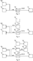
- Figure 4 shows an embodiment of a modified security architecture of the processing system 10a.
- the processing system 10a comprises means for overwriting one or more of the protections when a specific password is provided.
- some protections 150 once activated, may also not be deactivated anymore, or a given password may only deactivate a given sub-set of protections. For example, read protected memory areas containing security related data, such as cryptographic keys, may never be accessed, even when a password is provided.
- At least one reference password/keyword RK is stored in some way in the processing system 10a.
- the reference password RK may be hardwired or stored in a non-volatile memory 104 of the processing system 10a, such as the non-volatile program memory 104a.
- the processing system 10a is preferably configured to limit read access to the memory area containing the reference password RK in order to ensure that the reference password RK is kept secret.
- possible solutions for storing a reference keyword in a non-volatile memory are described in the above cited Italian patent applications.
- the processing system 10a comprises moreover a password verification circuit 152.
- the user should be able to provide a password verification command VPW comprising a password/keyword K to the password verification circuit 152.
- the user may provide the password K to the password verification circuit 152 via software instructions executed by the processing unit 102 of the processing system 10a and/or via a communication interface 106b of the processing system 10a, such as via a CAN interface or a ( e.g ., JTAG) debug interface connected to an external debugger.
- the blocks 110, the password verification circuit 152, and the interface 106b and/or the processing unit 102 may be connected through a bus.
- the command CMD and the password verification command VPW may be transmitted over the same bus, specifying as target address either the address of a block 110 (for a command CMD) or the password verification circuit 152 (for a password verification command VPW).
- the password verification circuit 152 may obtain the reference password RK and compared the password K with the reference password RK and, in case the two passwords match, the password verification circuit 152 may generate an overwrite signal OW, which is sent to one or more protection circuit 150. Accordingly, in response to the overwrite signal OW, the protection circuit(s) 150 may deactivate at least part of the respective protection.
- the inventors have observed that, in particular in case the reference password(s) RK are stored in a non-volatile memory 104, such a dynamic access to reference password RK may be exposed to security risks.
- a non-volatile memory 104 usually, access to a non-volatile memory 104 goes through a reading path comprising elements and features such as memory caches or prefetching transactions, concurrent access to the same bus, etc. Accordingly, it is likely that the reference password RK read from the non-volatile memory remains latched in one of the intermediate components, and an attacker may gain access to the reference password RK by spying the latched password.
- non-volatile memory 104 have test modes used to run specific internal testing, which e.g. permit to monitor the current state of the memory cells.
- test modes used to run specific internal testing, which e.g. permit to monitor the current state of the memory cells.
- One possible example is a check of the voltage thresholds of the non-volatile memory cells. Accordingly, these modes may use specific internal conditions, for example some internal high voltage on some nodes of the logic, which prevent a concurrent reading operation from working properly, resulting into altered data being read.
- Figure 5 shows in this context an embodiment of a modified security architecture.
- the processing system 10a comprises moreover a password upload circuit 154 and a temporary password repository 156.
- the password verification circuit 152 does not access dynamically the original reference password(s) RK, which is hardwired or preferably stored in the non-volatile memory 104.
- the password upload circuit 154 reads the reference password(s) RK once and stores the reference password(s) RK in the temporary password repository 156, which is implemented either with registers or with a RAM, which may only be read by the password verification circuit 152.
- the password verification circuit 152 may compare the received password K with a reference password RK stored in the temporary password repository 156, wherein the read path between the password verification circuit 152 and the temporary password repository 156 is not shared with other resources of the processing system 10a and accordingly may not be spied.
- the protections may be activated and similarly also the blocks 110 may be configured based on life cycle data LCD and/or configuration data CD.
- Figure 6 shows an embodiment of a processing system 10a, wherein the configuration data CD may be written into specific areas of a non-volatile memory 104 and retrieved when the processing system 10a is powered on.
- the configuration data CD may be stored in the non-volatile program memory 104a and/or an additional non-volatile memory, such as a one-time programmable (OTP) memory, e.g. implemented with fuses.
- OTP one-time programmable
- the program memory 104a may be used, in case the blocks shown in Figure 2 are integrated in a common integrated circuit.
- an additional non-volatile memory may be used, in case the program memory 104a is an external memory, and only the other blocks are integrated in a common integrated circuit.
- the configuration data CD are stored in a non-volatile memory 104 (non-volatile program memory 104a and/or a further non-volatile memory) of the integrated circuit comprising the blocks 110 requiring configuration data.
- such configuration data CD may include calibration data used to guarantee that the hardware behavior is uniform, thereby compensating possible production process tolerances. For example, this applies often to the calibration of analog components of the processing system, such as a temperature sensor, analog-to-digital converter, voltage reference, etc.
- the configuration data CD may also be used to customize the behavior of the hardware, e.g., the hardware blocks 110 and/or the protection circuits 150, according to different application needs. For example, as mentioned before, once the firmware of the processing system 10a has been stored in the processing system 10a, some configuration data CD may be written in order to deactivate the debug interface, which e.g. could be used to download the firmware of the processing system 10a.
- a first part of the configuration data CD may be written by the producer of the hardware of the processing system (e.g., the producer of an integrated circuit), and/or a second part of the configuration data CD may be written by the developer of the firmware of the processing system 10a.
- the programmed configuration data CD are read during a configuration phase, which usually starts as soon as the processing system 10a is powered on.
- the processing system 10a may comprise for this purpose a configuration module 108 configured to read the configuration data CD from the non-volatile memory 104, and distribute these configuration data CD within the processing system 10a.
- the configuration data CD are stored in reserved memory areas, e.g. in the form of a plurality of consecutive memory locations.
- the configuration module 108 accesses the reserved memory areas containing the configuration data CD, reads the configuration data CD and transmits the configuration data CD to a respective block 110 and/or protection circuit 150 within the processing system 10a.
- the block 110 may correspond to any block of the processing system 10a requiring configuration data and may correspond to the processing unit 102, a hardware resource 106 or even a memory ( e.g . the memory 104a).
- each block 110 and each protection circuit 150 may have associated a respective configuration data client 112.
- each configuration data client 112 may be associated univocally with a single hardware block 110 or a single protection circuit 150, and provide configuration data only to the associated hardware block 110 or protection circuit 150, e.g . a specific hardware resource 106.
- the configuration data client 112 may also be associated with a plurality of hardware blocks 110 and/or protection circuits 150.
- the same configuration data client 112 is used to provide configuration data CD to a hardware block 110 and the protection circuit 150 associated with this hardware block 110.
- the configuration data clients may also be integrated in the respective hardware block 110 or protection circuit 150.
- the configuration module 108 may determine for each target block 110/150 to be configured the respective configuration data (selected from the configuration data CD) and transmit the configuration data associated with the target block 110/150 to the configuration data client 112 associated with the target block 110/150.
- the configuration module 108 may determine the target block(s) for the current configuration information and send the current configuration data to the configuration data client(s) associated with the respective target block(s).
- any communication may be used for transmitting the configuration data CD to the configuration data clients 112, including both serial and parallel communications.
- the configuration module 108 and the configuration data clients 112 may be connected via a bus 114, and each configuration data client 112 may have associated a respective target address.
- each configuration data client 112 is configured to receive the configuration data from the module 108, store them into internal register, e.g. store them into one or more internal flip-flops or latches. The data stored in the register may then be used to generate one or more signals, which influence the behavior of one or more hardware blocks 110 and/or protection circuits 150.
- the above describe mechanism is also used to transmit the reference passwords RK to the temporary password repository 156.
- the reference password(s) RK are stored together with the configuration data CD in the memory 104, and a configuration data client 112c is associated (preferably univocally) with the temporary password repository 156.
- the configuration module 108 reads also the reference password(s) RK together with the other configuration data CD from the memory 112 and sends the reference password(s) RK to the configuration data client 112c associated with the temporary password repository 156, thereby loading the reference password(s) RK into the temporary password repository 156.
- Figure 7 shows in this respect a possible embodiment of the communication between the configuration module 108 and the configuration data clients 112.
- the processing system 10a comprises a configuration module 108 configured to read the configuration data CD from one or more non-volatile memories 104 and a plurality of configuration data clients 112 configured to receive respective configuration data CD from the configuration module 108 and distribute them among the blocks 110/150/156 requiring configuration data.
- each configuration data client 112 may be associate univocally with a respective block 110/150/156.
- the processing system 10a comprises again three configuration data clients 112a, 112b and 112c.
- the configuration module 108 comprises a data read module 1080 configured to read the configuration data CD from the memory 104 and a dispatch module 1082 configured to transmit the configuration data to the configuration data clients 112.
- any communication may be used for communication between the dispatch module 1082 and the configuration data clients 112.
- the communication between the dispatch module 1082 and the configuration data clients 112 is based on data frames in accordance with a given format, called in the following Device Configuration Format (DCF).
- DCF Device Configuration Format
- each data frame comprises two fields: the payload (i.e., the real data), called DCF Format payload, and possible additional data attributes used to identify the receiver of the data, called DCF Format attributes, wherein the receiver is one of the configuration data clients 112 representing a DCF client.
- the data attributes may consist in 16 or 32 bits, wherein a given number of bits specifies the address of one of the configuration data clients 112, and the payload may consist in 16 or 32 bits.
- the data read module 1080 is configured to read blocks of 64 bits from the memory 104, wherein the first 32 bits contain the data attributes (including the address of a configuration data client) and the second 32 bits contain the configuration data to be transmitted to the address specified in the data attributes.
- each configuration data client/DCF client 112 may be a hardware module, usually comprising a combinational circuit configured to store the received data in an internal register implemented, e.g., with flip-flops/latches, thereby permitting to distribute, via one or more internal signals generated as a function of the data stored in the internal register, the configuration data received to various parts of the associate hardware block(s) 110/150/156.
- each configuration data client 112 may have associated a univocal address (i.e., univocal within each processing system 10a) and analyses the data transmitted by the dispatch module 1082 in order to determine whether the additional data attributes (DCF Format attributes) contain the address associated with the configuration data client 112.
- the module 108 may also comprises a state control module 1084 configured to manage the various configuration phases of the processing system 10a.
- a reset module 116 of the processing system 10a may generate a reset signal RESET, which is used to perform a reset of the various components of the processing system 10a.
- the reset signal RESET may correspond to a reset pulse of a given number of clock cycles, provided to the blocks 110 of the processing system 10a.
- the reset signal RESET may be used by the configuration data clients 112 in order to set the internal register to a given reset value.
- the state control module 1084 may activate the configuration phase. Specifically, during the configuration phase, the data read module 1080 may read the configuration data CD from the memory 104 and the dispatch module 1082 may send the configuration data CD to the various configuration data clients 112, thereby overwriting the reset values.
- the dispatch module 1082 may generate a data signal DATA having a given number of bits (corresponding to the bits of the payload) containing the configuration data to be transmitted to a given configuration data client 112 and further control signals for selecting the target configuration data client 112.
- the dispatch module 1082 generates also an address signal ADR containing the address of the target configuration data client 112 and optionally a chip select signal CS used to signal that the address signal ADR and the data signal DATA are valid.
- the address signal ADR (and the chip select signal CS) may be provided to a decoder 124 configured to activate one of the configuration data clients 112 as a function of the address signal ADD.
- the decoder 124 may set a chip select signal CSa in order to indicate that the configuration data client 112a should read the data signal DATA when the address signal ADR corresponds to an address assigned to the configuration data client 112a (and the chip select signal CS is set).
- the decoder 124 may set a chip select signal CSb in order to indicate that the configuration data client 112b should read the data signal DATA when the address signal ADR corresponds to an address assigned to the configuration data client 112b (and the chip select signal CS is set), etc.
- the configuration data CD may also comprise security configuration data used to configure the protections 150, such as the external access to a debug interface or the (read and/or write) access to given memory locations, and the reference passwords RK to be stored in the temporary password repository 156.
- configuration data CD may comprise two sub-sets of configuration data:
- these groups of configuration data are written to different areas of the memory(ies) 104, thereby permitting that these groups may be configured independently.
- the security configuration data included in the first group of configuration data may also permit to set the access rights to the memory locations, in which the first group of configuration data are stored.
- the first group of configuration data may not be overwritten, and/or the memory interface may inhibit a read access to the first group of configuration data (e.g., by the processing unit 102).
- the security configuration data included in the second group of configuration data may be used to configure the behavior of the blocks 110 from a functional point of view, e.g. in order to enable or disable the debug interface, etc.
- the second group of configuration data may not be overwritten or read.
- the reference password(s) used to unblock the protections may be configured together with the first group and/or secondo group of configuration data.
- the first group may contain a reference password for performing access operations to read and/or write protected memory locations and the second group may contain a reference password for enabling again the debug interface.
- the reset/configuration phase of the processing system 10a is used to store one or more reference passwords RK into a private/local memory (e.g., a RAM) of the temporary password repository 156.
- a private/local memory e.g., a RAM
- the reference passwords RK may be generated during the production phase and programmed into some area of the non-volatile memory 104 (for example some specific memory locations of the program memory 104a).
- the reference password(s) RK are read from the non-volatile memory 104 and distributed to the temporary password repository 156 via dedicated hardware components 108 and 112, e.g. by using the DCF data format.
- the DCF data format permits to transfer different information, programmed inside the non-volatile memory, to various blocks within the processing system 10a using the same data bus. Specifically, each piece of configuration data is inserted in a frame together with the identifier/address of a configuration data client 112.
- the hardware configuration module 108 reads all theses DCF data frames programmed in the non-volatile memory 104 and sends them to the respective configuration data clients 112.
- the reference password(s) RK may be stored in temporary password repository 156.
- the temporary password repository 156 may comprises one or more slots PW0, PW1, ..., each slot being adapted to store a respective reference password RK.
- a single configuration data client 112c is associated with the temporary password repository 156.
- a plurality of DCF frames (each comprising a respective reference password RK) may be sent in sequence to the address of the configured data client 112c and, once a reference password RK is received, the temporary password repository 156 may store the reference password into a respective slot PW0, PW1, ... of the internal memory.
- the DCF frame may also include a field indicating the slot number, where the respective reference password RK should be stored.
- the configuration data clients 112 may also be used directly as memory of the temporary password repository 152.
- these registers may also be used directly as memory of the temporary password repository 152.
- a plurality of configuration data clients 112c may be associated with the temporary password repository 152, wherein each configuration data clients 112c has a respective (univocal) address.
- a plurality of DCF frames (each comprising a respective reference password RK) may be sent in sequence to the addresses of the configured data clients 112c.
- the use of a RAM is advisable when a lot of reference password RK have to be stored into the temporary password repository 156 and/or when the passwords are long.
- the internal register of one or more configuration data clients 112c may be used when only a single reference password RK has to be stored.
- the reference passwords RK are stored in the memory of the temporary password repository 152. Accordingly, there is no need to further access the reference passwords RK stored in the non-volatile memory 104 upon a password challenge request. Accordingly, in the embodiment considered, the communication may not be spied by other blocks of the processing system 10a, because the other blocks are not operative during the configuration phase of the processing system 10a.
- Figure 8 shows an embodiment of the password verification circuit 152.
- the password verification circuit 152 is connected (e.g., directly) to the temporary password repository 156 for receiving a reference password RK to be used for a password verification operation.
- the reference password(s) RK are stored in dedicated areas of the non-volatile memory 104 of the processing system 10a.
- theses reference password(s) RK may be programmed during the production phase.
- the reference password (s) RK may be read (e.g., together with other configuration data CD) by the hardware configuration module 108 of the processing system 10a and distributed to the various configuration data clients 112 within the processing system 10a.
- the distribution of the configuration data CD including the reference password(s) RK may occur during a configuration phase, i.e. when the processing unit 102 and the other blocks (such as communication interfaces 106b) are not yet operative and only the configuration module 108 and the configuration data clients 112 are active.
- the reference password(s) RK are already loaded into the temporary password repository 156, when the processing unit 102 is activated.
- the temporary password repository may contain only a single reference password.
- Figure 9 shows an embodiment, in which the temporary password repository 156 comprises a plurality of slots PW0, PW1, etc. for storing a plurality of reference passwords RK.
- the password verification circuit 152 comprises at least one interface for receiving a password K to be verified.
- the password verification circuit 152 may receive a password verification command VPW including a password K from the processing unit 102 of the processing system 10a.
- the password verification circuit 152 may comprise an interface 1520.
- the processing unit 102 is a microprocessor and the interface 1520 comprises one or more register addressable by the processing unit 102, such as so called special function registers of the processing unit 102.
- the processing unit 102 may provide data to the password verification circuit 152 by writing the content of the registers 1520 via software instructions.
- the password verification circuit 152 may receive data via a communication interface 106b, e.g., from another resource 106 of the processing system 10a or an external processing unit 30.
- a communication interface 106b e.g., from another resource 106 of the processing system 10a or an external processing unit 30.
- the interface 106b may a debug interface, such as a JTAG interface, connected to an external debugger 30.
- the (e.g. debug) interface 106b may indeed be split into a plurality of sub-interfaces connected through a bus 1062, wherein each sub-interface is associated with a respective block of the processing system 10a to be controlled via the ( e . g . debug) interface.
- the interface 1060 which may only manage the debug commands addressed to the password verification circuit 152.
- the interface 1520 or 1060 may thus provide a password verification command VPW including a password K to be verified.
- VPW password verification command
- the interface 1060 may provide a password Ka
- the interface 1520 may provide a password Kb.
- these passwords Ka and Kb are then provided to a multiplexer 1526 configured to select either the password Ka or Kb (based on whether the interface 1060 or 1520 is used).
- the temporary password repository 156 comprises a plurality of slots PW0, PW1,....
- the password verification command VPW may include, and similarly the interfaces 1520 and/or 1060 may provide, additional password configuration data CFG associated with the respective password K to be verified.
- the interface 1060 may provide password configuration information CFGa
- the interface 1520 may provide a password configuration information CFGb.
- the respective password configuration information CFGa and CFGb are then provided to a multiplexer 1528 configured to select either the additional password configuration data CFGa or CFGb (based on whether the interface 1060 or 1520 is used).
- the additional password configuration data CFG may contain a slot number SLOT indicating the slot PW0, PW1, ... of a reference password RK in the temporary password repository 156 to be used for the verification.
- the temporary password repository 156 may provide the respective reference password RK stored in the slot PW0, PW1, ... indicated by the slot number SLOT.
- the password K received via the interface 1060/1520 and the (selected) reference password RK obtained from the temporary password repository 156 are provided to a comparison circuit 1522 configured to determine whether the password K corresponds to the (selected) reference password RK. In case the password K corresponds to the (selected) reference password RK, the comparison circuit 1522 generates an overwrite signal OW indicating that the password K is correct, i.e. the password K corresponds to the (selected) reference password RK.
- the password verification circuit 152 supports only a single reference password RK (i.e., the temporary password repository comprises only a single slot).
- the signal OW may be sent directly to one or more of the protections circuits 150, which thus may deactivate the respective protection.
- each protection circuit 150 may not only take into account the signal OW, but also further configuration information, such as the previously mentioned life cycle data LCD and/or configuration data CD, which may indicate whether the protection may indeed be deactivated or not by means of the signal OW.
- the password verification circuit 152 supports a plurality of reference passwords RK (i.e., the temporary password repository 156 comprises a plurality of slots).
- the signal OW may be sent to a circuit 1524.
- the circuit 1524 is configured to generate a plurality of overwrite signals OW0, OW1, ... as a function of the signal OW and the slot number SLOT.
- the block 1524 may be implemented with a combinational circuit or a look-up table.
- a respective overwrite signal OW0, OW1, ... is associated with each slot, and only the overwrite signal OW0, OW1, ... associated with the currently used slot SLOT is set (e.g., to the logic level high) when the password K and RK match.
- the circuit 1524 may also comprises registers, e.g. flip-flops or latches, for storing the values of the overwrite signal OW0, OW1, ..., thereby maintain the value of the overwrite signals OW0, OW1, ... when a new password verification is requested.
- the overwrite signals OW0, OW1, ... may then be provided to the various protection circuits 150, which thus may deactivate the respective protection.
- a respective overwrite signal OW0, OW1, ... may be associated with each protection circuit 150, or each overwrite signal OW0, OW1, ... may be associated also with a plurality of protection circuits 150.
- the circuit 1524 is configured to associate with each slot number a respective subset of protection circuits 150. Moreover, when the password received K corresponds to the reference password RK for a given slot SLOT, the circuit 1524 generates one or more signals OW0, OW1, ... in order to inform the subset of protection circuits 150 associated with the given slot SLOT that the passwords match.
- each protection circuit 150 may deactivate the respective protection not only as a function of the respective signal OW, but also as a function of further configuration information, such as the previously mentioned life cycle data LCD or configuration data CD, which may indicate whether the protection may be deactivated or not by means of the password verification.
- each slot PW0, PW1, ... contains a given reference password RK and the slot index SLOT determines (via the circuit 1524), which protection circuit 150 is regulated by the password.
- a given slot number e.g ., slot 3
- the protection circuit 150 controlling access to the debug interface, e.g ., the access of the external debugger 30 to the debug bus 1062.
- a given slot number e.g ., slot 2
- the protection circuit 150 regulating read and/or write access to the non-volatile memory 104.
- a given slot number (e.g ., slot 1) may represent also a master password (e.g ., written by the producer of the processing system 10a), which is associated with all protection circuits 150. Accordingly, neglecting that also further life cycle data LCD and/or configuration data CD may be taken into account, a protection may be removed by providing the correct password stored in a slot associated with the respective protection 150.
- the password management is split into three functional blocks:
- the temporary password repository 156 is used as a secure repository for the reference passwords RK, while the password verification circuit 152 processes password challenge requests received via the interfaces 1060 and/or 1520 and provides the result to the connected protection circuits 150.
- the password challenge requests i.e. the password verification commands VPW
- the password verification commands VPW may be received:
- the interfaces 1520 and 1060 have the same basic functionality, i.e ., provide a password K and possible additional configuration information CFG to the password verification circuit 152.
- a single interface could be used, e.g., in case the processing unit 102 is also connected to the bus 1062.
- the interface 1520 may be a register interface specifically adapted to interface the processing unit 102.
- the interface 1520 may be a special function register of a microprocessor and programmed directly via software instructions executed by the processing unit 102.
- the interface 1060 may be part of debug interface 106b, such as a JTAG interface.
- various blocks of the processing system may have associated debug interfaces, which may also be connected through a debug bus 1062. Accordingly, a certain protection mechanism could be removed by providing a proper password through this debug interface (in case at least the portion 1060 of the debug interface associated with the password verification circuit 152 is not deactivated).
- a protection circuit 150 could be configured to deactivate the debug interface of the processing unit 102, e.g., based on the life cycle data LCD and/or the configuration data CD.
- the debug interface of the processing unit 102 may be connected to the bus 1062.
- an external debugger 30 could be used to provide a password K to the debug interface 1060 of the password verification circuit 152 and the password verification circuit 152 may generate the signal OW (or similarly one or more signals OW0, OW1, etc.), which is sent to the protection circuit 150 associated with the debug interface of the processing unit 102.
- the protection circuit 150 may then reactivate the debug interface of the processing unit 102, and a developer may use the external debugger 30 to analyze the processing unit 102.
- the interface 1060 may be part of the (e.g., debug) interface 106b.
- the specific protocol used to write data to the interface 1060 depends on the specific implementation of the interface 106b.
- the most common protocols are based on request and busy signals.
- the busy signal may be set by the password verification circuit 152 to communicate that the password verification circuit is performing already an operation, i.e. no password challenge requests are accepted.
- the request signal may be set by the hardware client requesting a password challenge (only after the busy signal has been de-asserted).
- the hardware client requesting a password challenge provides the password verification command VPW including the password to be verified K and if supported the additional password configuration information CFG, such as the password slot number SLOT.
- the register interface 1520 may comprise a busy flag, to advice the processing unit 102 when the password verification circuit 152 is busy, and means for starting a challenge operation (such as a request flag), a register for storing the password to be verified K and optionally the further configuration data, in particular the slot index SLOT.
- Figure 10 shows an embodiment of the register interface 1520.
- the interface 1520 comprises:
- the processing unit 102 may execute the following steps:
- the password verification circuit 152 may set the busy flag in order to indicate that the password verification circuit 152 does not accepts any other password challenge request.
- the comparison circuit 1522 If the password K provided by the client matches the reference password RK stored in the given slot SLOT, then the comparison circuit 1522 generates the overwrite signal OW indicating that the access may be granted.
- the block 1524 may also provide respective overwrite signals OW0, OW1, ... only for a subset of the protection circuits 150.
- the protection circuit 150 may decide whether the protection should indeed be disabled.
- each protection circuit 150 may take into account for this purpose the life cycle data LCD and/or the configuration data CD.
- each protection circuit 150 may take into account also the identity of the circuit having requested the password verification.
- the interface 1520 accepts only requests from the processing unit 102. Accordingly, the identity of the requesting circuit may be determined implicitly.
- the interface 1060 may be connected to a bus 1062. Accordingly, in this case, each device connected to the bus 1062 may be identified with a given address (being univocal within the processing system 10a).
- the interface 1520 may be connected to a bus, e.g. in case the processing system 10a comprises a plurality of processing units, such as a plurality of microprocessors.
- the identity of the circuit requesting the verification of a password may correspond to the univocal address of the block within the processing system 10a and will be called in the following master identification MID.
- Figure 11 shows an embodiment, wherein this identification MID is provided by the interfaces 1060 and 1520 together with the additional configuration information CFG.
- the number of the overwrite signal OW0, OW1, ... corresponds to the number N of slots in the temporary password repository 156, i.e ., a respective signal OW0, OW1, ... is univocally associated with a respective slot. Accordingly, by providing the correct password K for a given slot SLOT, only the respective overwrite signal OW0, OW1, ... will be set, e.g ., the signal OW0 will be set for the password PW0, the signal OW1 will be set for the password PW1, etc. As mentioned before, the overwrite signals OW0, OW1, ... may also be stored in registers, thereby permitting that plural overwrite signal OW0, OW1, ... may be set by providing sequentially the passwords for the various slots.
- the block 1524 when setting an overwrite signal OW0, OW1, ..., stores for the specific overwrite signal OW0, OW1, ... also the identification MID of the circuit having requested the password verification, i.e . the circuit 1524 provides indeed N identification MID0, MID1, .... Accordingly, in the embodiment considered, once having verified that the password K corresponds to the reference password RK for the selected SLOT, not only the respective overwrite signal is set, but also the current identification MID is stored as the identification MID0, MID1, ... associated with the respective SLOT.
- the protection circuits 150 do not receive only the overwrite signal OW0, OW1, ..., but also the respective identification MID0, MID1, ....
- each password slot PW0, PW1, ... may be associated univocally with a single protection circuit 150, i.e. each password may only unblock the respective protection circuit 150. Accordingly, also the overwrite signal and the respective IDs MID associated with a given slot have to be provided only to the respective protection circuit 150.
- the number of slots N may be defined at design time, depending on how many protection circuits 150 with an associated password-dependent protection mechanism exist. Moreover, it is also simple to add a new additional protection circuit 150, by just adding a new reference password slot, and a new overwrite signal OV and identification MID output.
- the protection circuits 150 may use the identification MID for different purposes.
- a protection circuit 150 may disable the protection only when the request comes from a circuit having a given identification MID. For example, in case of a multiprocessor system, when the request comes from a given microprocessor 102.
- the protection circuit 150 may verify whether a given access request to the block 110 associated with the protection circuit (see also Figure 5 ) has the same identification MID as the circuit having requested the password verification. Accordingly, the identification MID can be used by the protection circuits 150 to limit the access to the protected resource 110 only to the circuit identified by the same identification MID, thereby ensuring that only the circuit having provided the correct password may also access the respective protected resource 110.
- a first circuit may deactivate a first protection 150 by providing the first reference password PW0, and a second circuit may deactivate a second protection by providing the second reference password PW1, wherein the second circuit does not have access to the first protection.
- the password verification circuit 152 may verify whether the password K provided by the requester client has a special value (e.g., all-1, all-0, etc.) which will result always in a comparison failure.
- a special value e.g., all-1, all-0, etc.
Description
- Embodiments of the present disclosure relate to processing systems, such as micro-controllers.
-
Figure 1 shows a typical electronic system, such as the electronic system of a vehicle, comprising a plurality ofprocessing systems 10, such as embedded systems or integrated circuits, e.g., a FPGA (Field Programmable Gate Array), DSP (Digital Signal Processor) or a micro-controller (e.g., dedicated to the automotive market). - For example, in
Figure 1 are shown threeprocessing systems suitable communication system 20. For example, the communication system may include a vehicle control bus, such as a CAN (Controller Area Network) bus, and possibly a multimedia bus, such as a MOST (Media Oriented Systems Transport) bus, connected to vehicle control bus via a gateway. Typically, theprocessing systems 10 are located at different positions of the vehicle and may include, e.g., an Engine Control Unit (ECU), a Transmission Control Unit (TCU), an Anti-lock Braking System (ABS), a body control modules (BCM), and/or a navigation and/or multimedia audio system. - Future generations of processing systems, in particular micro-controllers dedicated to automotive applications, will exhibit a significant increase in complexity, mainly due to the increasing number of functionalities (such as new protocols, new features, etc.) and to the tight constraints concerning the operation conditions of the system (such as lower power consumption, increased calculation power and speed, etc.).
- In parallel, the security framework of each
processing system 10 becomes also more and more complex, which determines an increase of the time and complexity of the testing phase, needed to guarantee the functionality and robustness of the security framework. - Generally, the security framework is based on the concept of resource protection, i.e., given a set of resources, the framework is designed so that the access to one or more resources may be selectively blocked or granted under based on specific conditions. For example, one of these conditions may be based on a password, i.e. access to the resource is blocked until the correct password is provided.
- Specifically, the present invention relates to a processing system comprising a password verification circuit according to the preamble of Claim 1, which is known, e.g. from document
US 2013/019305 A1 . DocumentUS 2009/158444 A1 may also be of interest for the present invention. - In view of the above, it is an objective of various embodiments of the present disclosure to provide solutions able to handle the password management within a processing system, such as a micro-controller.
- According to one or more embodiments, one or more of the above objectives is achieved by means of a processing system having the features specifically set forth in the claims that follow. Embodiments moreover concern a related integrated circuit.
- The claims are an integral part of the technical teaching of the disclosure provided herein.
- As mentioned before, various embodiments of the present disclosure relate to a processing system. As usual, such processing system may comprise one or more processing units, such as microprocessors, volatile and non-volatile memories, and further resources.
- Specifically, in various embodiments, the processing system comprises a non-volatile memory adapted to store at least one reference password, such as the program memory of the microprocessor.
- In various embodiments, the processing system comprises moreover a hardware block, such as a processing unit, a memory or a resource, and a protection circuit associated with the hardware block. Specifically, the protection circuit is configured to receive a control command for the associated hardware block and selectively forward the control command to the associated hardware block, thereby controlling access to the associated hardware block, e.g., by means of a debug interface or another block of the processing system. For example, in various embodiments, the access control may be configured by means of life cycle data and/or configuration data.
- In various embodiments, the protection circuit may also control the access as a function of an overwrite signal provided by a password verification circuit, i.e. the protection circuit may selectively forward the control command to the associated hardware block as a function of the overwrite signal provided by the password verification circuit, e.g., in order to permit access when the overwrite signal indicates that a password verification operation was successful.
- Specifically, in various embodiments, the password verification circuit is configured to receive a password verification command including a password. Similar to the control command, also the password verification command may be provided by another block of the processing system, such as a processing unit and/or a communication interface.
- In various embodiments, the password verification circuit obtain then one of the at least one reference password stored in the non-volatile memory and tests whether the password received and the reference password correspond. Finally, when the passwords correspond, the password verification circuit may generate the overwrite signal.
- Specifically, in various embodiments, the reference password is not obtained dynamically from the non-volatile memory for each password verification operation, but the processing system comprises a temporary password repository including a memory adapted to store the at least one reference password, and a password upload circuit configured to read the at least one reference password once from the non-volatile memory, e.g., during the start-up of the processing system, and store the at least one reference password read from the non-volatile memory in the temporary password repository. Accordingly, in various embodiments, the password verification circuit may obtain the reference password from the temporary password repository.
- Generally, the temporary password repository may also comprise a plurality of slots for storing a plurality of reference passwords. In this case, the password verification command may include a field for specifying a slot number and the temporary password repository may provide the reference password stored in the slot indicated by the slot number. Similarly, the password verification circuit may generate for each slot a respective overwrite signal indicating that the password received and the reference password stored in the slot indicated by the slot number correspond.
- In various embodiments, the reference password(s) are read from the non-volatile memory and stored in the temporary password repository when the processing system is switched on and the other blocks, in particular the processing unit and/or the communication interface, are not operative yet.
- For example, in various embodiments, the processing system comprises at least one hardware block and/or protection circuit configured to change operation as a function of configuration data. For example, as mentioned before, the access control implemented in the protection circuit may be configured by means of these configuration data. Specifically, in various embodiments, these configuration data may also be stored in the non-volatile memory. For example, in various embodiments, the processing system may comprise at least one first configuration data client associated with this at least one hardware block and/or protection circuit, wherein the at least one first configuration data client is configured to receive configuration data and provide the configuration data received to the associated at least one hardware block and/or protection circuit. The processing system comprises also a hardware configuration module configured to read the configuration data from the non-volatile memory and transmit the configuration data to the at least one first configuration data client.
- In various embodiments, the reference password(s) are stored together with this configuration data in the non-volatile memory, i.e. the reference password(s) are part of the configuration data. In this case, the processing system may comprise at least one second configuration data client associated with the temporary password repository, i.e., the at least one second configuration data client is configured to receive configuration data from the hardware configuration module and provide the configuration data to the temporary password repository, whereby when the hardware configuration module reads the configuration data from the non-volatile memory, the hardware configuration module transmits the at least one reference password to the at least one second configuration data client associated with the temporary password repository.
- As mentioned before, in various embodiments, the reference password(s) are loaded into the temporary password repository during the start-up of the processing system. For this purpose, the processing system may comprise a reset circuit configured to generate a reset signal when said processing system is switched on. The hardware configuration module may thus read the configuration data from the non-volatile memory and transmit the configuration data to the at least one first and second configuration data client in response to the reset signal.
- As mentioned before, the control command and/or the the password verification command may be provided by another block of the processing system, such as a processing unit and/or a communication interface.
- For example, in various embodiment, the processing system comprises a communication bus, such as a JTAG bus, wherein the hardware block to be controlled is connected to the communication bus via the associated protection circuit in order to receive the control command. Similarly, the password verification circuit may comprise a first interface connected to this communication bus for receiving the password verification command.
- In addition or alternatively, the password verification circuit may comprise a second interface for receiving the password verification command (e.g., directly) from said processing unit. This is particularly useful when the processing unit is a microprocessor, because in this case the second interface may comprise at least one register addressable by the microprocessor via software instructions.
- In various embodiment, in order to improve security, when the password and the one reference password correspond, the password verification circuit may transmit (in addition to the overwrite signal) a signal containing an identification of the device, e.g., the processing unit and/or the device connected to the communication interface, having provided the password verification command. For example, the password verification circuit may extract this identification from the password verification command.
- Accordingly, in various embodiments, once at least one reference password has been stored in the non-volatile memory and the processing system has been started, the password upload circuit will automatically read the reference password(s) from the non-volatile memory and store the reference password(s) in the temporary password repository. Next, the password verification circuit may receive a password verification command including a password from the processing unit and/or the communication interface. In response to this password verification command, the password verification circuit obtains one of the reference password(s) from the temporary password repository and tests whether the password received and the one reference password correspond. Finally, when the passwords correspond, the password verification circuit may transmit an overwrite signal to a protection circuit of said processing system.
- Embodiments of the present disclosure will now be described with reference to the annexed drawings, which are provided purely by way of non-limiting example and in which:
-
Figure 1 shows a typical electronic system; -
Figure 2 shows an embodiment of a processing system; -
Figure 3 shows a first embodiment of the security architecture of a processing system; -
Figure 4 shows a second embodiment of the security architecture of a processing system comprising a password verification circuit; -
Figure 5 shows a third embodiment of the security architecture of a processing system comprising a password verification circuit and a temporary password repository; -
Figures 6 and 7 show embodiments of a processing system comprising a configuration module and configuration data clients for loading reference password into the temporary password repository ofFigure 5 ; and -
Figures 8 to 11 show embodiments of the password verification circuit ofFigure 5 . - In the following description, numerous specific details are given to provide a thorough understanding of embodiments. The embodiments can be practiced without one or several specific details, or with other methods, components, materials, etc. In other instances, well-known structures, materials, or operations are not shown or described in detail to avoid obscuring aspects of the embodiments.
- Reference throughout this specification to "one embodiment" or "an embodiment" means that a particular feature, structure, or characteristic described in connection with the embodiment is included in at least one embodiment. Thus, the appearances of the phrases "in one embodiment" or "in an embodiment" in various places throughout this specification are not necessarily all referring to the same embodiment. Furthermore, the particular features, structures, or characteristics may be combined in any suitable manner in one or more embodiments.
- The headings provided herein are for convenience only and do not interpret the scope or meaning of the embodiments.
- In the following
Figures 2 to 11 parts, elements or components which have already been described with reference toFigure 1 are denoted by the same references previously used in such Figure; the description of such previously described elements will not be repeated in the following in order not to overburden the present detailed description. -
Figure 2 shows a block diagram of an embodiment of adigital processing system 10a, such as a micro-controller. - In the embodiment considered, the
processing system 10a comprises at least oneprocessing unit 102, such as a microprocessor, usually the Central Processing Unit (CPU), programmed via software instructions. Usually, the software executed by theprocessing unit 102 is stored in aprogram memory 104a, such as a non-volatile memory, such as a Flash memory or EEPROM. Generally, thememory 104a may be integrated with theprocessing unit 102 in a single integrated circuit, or thememory 104a may be in the form of a separate integrated circuit and connected to theprocessing unit 102, e.g. via the traces of a printed circuit board. Thus, in general thememory 104a contains the firmware for theprocessing unit 102, wherein the term firmware includes both the software of a microprocessor and the programming data of a programmable logic circuit, such as a FPGA. - In the embodiment considered, the
processing unit 102 may have associated one ormore resources 106, such as: - one or
more memories 106a, such as a Random Access Memory (RAM), - one or
more communication interfaces 106b, such as an UART (Universal asynchronous receiver/transmitter), SPI (Serial Peripheral Interface Bus), I2C (Inter-Integrated Circuit), CAN bus (Controller Area Network), Ethernet, and/or debug interface; and/or - one or more
further resources 106c, such as:- a) analog-to-digital and/or digital-to-analog converters; and/or
- b) one or more dedicated digital components, such as hardware timers and/or counters, or a cryptographic co-processor; and/or
- c) one or more analog components, such as comparators, sensors, such as a temperature sensor, etc.; and/or
- d) one or more mixed signal components, such as a PWM (Pulse-Width Modulation) driver.
- Accordingly, the
digital processing system 10a may support different functionalities. For example, the processing systems may have different hardware architectures. For example, theprocessing units 102 may have different architectures and processing speeds, and/or the number and type of thehardware resources 106 may vary. Moreover, the behavior of theprocessing unit 102 is determined by the firmware stored in thememory 104a, e.g., the software instructions to be executed by amicroprocessor 102 of amicrocontroller 10a. Thus, by installing a different firmware, the same hardware (micro-controller) can be used for different applications. -
Figure 3 shows an embodiment of the security architecture of theprocessing system 10a. - As mentioned before, the security architecture of a
processing system 10a, such as a microcontroller, is aimed to limit access to one or more of theresources 110 of the processing system, such as theprogram memory 104a, theprocessing unit 102 and/or one ormore resources 106. - For example, as shown in
Figure 3 , one or more of theresources 110 of the processing system may have associated aprotection circuit 150 configured to control access to therespective resource 110. For example, respective access requests CMD may be received from anotherresource 110 of theprocessing system 10a, such as theprocessing unit 102 and/or acommunication interface 106b, such as a debug interface. - For example, in various embodiments, the
protection circuits 150 may control the access to one or moreinternal resources 110 of theprocessing system 10a via an external debug tool, or the possibility to perform a write (or similarly a read) access to specific memory areas, such as memory areas of thenon-volatile memory 104a. For example, the use of the debug interface, such as a JTAG (Joint Test Action Group) interface, may be deactivated by interrupting (via the protection circuit 150) the connection of the internal debug interface to the pins to which an external debugger may be connected. Accordingly, in this way, the debug interface will not respond to external requests provided to the respective pins. - Generally, while some
resources 110 may possibly not have any access restrictions at all, the access toother resource 110 may be blocked (i.e. the protection may be activated) by default or selectively as a function of configuration data. For example, in various embodiments and as also described in detail in the Italian patent applicationsIT102017000062788 IT102017000062830 processing system 10a as indicated by life cycle data LCD and/or configuration data CD. For example, eachprotection 150 of theprocessing system 10a may be in one of the following states: - a) the life cycle data LCD indicate that the protection is disabled independently of the configuration data CD;
- b) the life cycle data LCD indicate that the protection may be enabled selectively and the configuration data CD indicate that the protections is disabled;
- c) the life cycle data LCD indicate that the protection may be enabled selectively and the configuration data indicate that the protections is enabled; or
- d) the life cycle data LCD indicate that the protection is enabled independently of the configuration data CD.
- In this regard, the above cited Italian patent applications also describe that the
processing system 10a may support a life cycle data overwrite function and/or a configuration data overwrite function. Accordingly, also the access to such overwrite functions may be limited by means of suitable protection mechanisms (see e.g. blocks 1088 and 1106 of the above cited Italian patent applications). -
Figure 4 shows an embodiment of a modified security architecture of theprocessing system 10a. - Specifically, in the embodiment considered, in order to grant access to protected resources, the
processing system 10a comprises means for overwriting one or more of the protections when a specific password is provided. Generally, someprotections 150, once activated, may also not be deactivated anymore, or a given password may only deactivate a given sub-set of protections. For example, read protected memory areas containing security related data, such as cryptographic keys, may never be accessed, even when a password is provided. - In the embodiment considered, at least one reference password/keyword RK is stored in some way in the
processing system 10a. For example, the reference password RK may be hardwired or stored in anon-volatile memory 104 of theprocessing system 10a, such as thenon-volatile program memory 104a. In the latter case, theprocessing system 10a is preferably configured to limit read access to the memory area containing the reference password RK in order to ensure that the reference password RK is kept secret. For example, possible solutions for storing a reference keyword in a non-volatile memory are described in the above cited Italian patent applications. - In the embodiment considered, the
processing system 10a comprises moreover apassword verification circuit 152. - Accordingly, in order to deactivate at least one protection, the user should be able to provide a password verification command VPW comprising a password/keyword K to the
password verification circuit 152. For example, in the embodiment considered, the user may provide the password K to thepassword verification circuit 152 via software instructions executed by theprocessing unit 102 of theprocessing system 10a and/or via acommunication interface 106b of theprocessing system 10a, such as via a CAN interface or a (e.g., JTAG) debug interface connected to an external debugger. - For example, in various embodiments, the
blocks 110, thepassword verification circuit 152, and theinterface 106b and/or theprocessing unit 102 may be connected through a bus. In this case, the command CMD and the password verification command VPW may be transmitted over the same bus, specifying as target address either the address of a block 110 (for a command CMD) or the password verification circuit 152 (for a password verification command VPW). - Accordingly, once the
password verification circuit 152 has received the password verification command VPW comprising the password K, thepassword verification circuit 152 may obtain the reference password RK and compared the password K with the reference password RK and, in case the two passwords match, thepassword verification circuit 152 may generate an overwrite signal OW, which is sent to one ormore protection circuit 150. Accordingly, in response to the overwrite signal OW, the protection circuit(s) 150 may deactivate at least part of the respective protection. - The inventors have observed that, in particular in case the reference password(s) RK are stored in a
non-volatile memory 104, such a dynamic access to reference password RK may be exposed to security risks. - For example, usually, access to a
non-volatile memory 104 goes through a reading path comprising elements and features such as memory caches or prefetching transactions, concurrent access to the same bus, etc. Accordingly, it is likely that the reference password RK read from the non-volatile memory remains latched in one of the intermediate components, and an attacker may gain access to the reference password RK by spying the latched password. - In addition, the fact that the reference password RK is read dynamically from the non-volatile memory permits that an attacker may put the
non-volatile memory 104 in a state, where it always returns the same and known value. Accordingly, in this way, the attacker could easily overwrite theprotections 150 by providing the known value. For example, oftennon-volatile memories 104 have test modes used to run specific internal testing, which e.g. permit to monitor the current state of the memory cells. One possible example is a check of the voltage thresholds of the non-volatile memory cells. Accordingly, these modes may use specific internal conditions, for example some internal high voltage on some nodes of the logic, which prevent a concurrent reading operation from working properly, resulting into altered data being read. -
Figure 5 shows in this context an embodiment of a modified security architecture. - Specifically, compared to
Figure 4 , theprocessing system 10a comprises moreover a password uploadcircuit 154 and atemporary password repository 156. - Accordingly, in the embodiment considered, the
password verification circuit 152 does not access dynamically the original reference password(s) RK, which is hardwired or preferably stored in thenon-volatile memory 104. Conversely, the password uploadcircuit 154 reads the reference password(s) RK once and stores the reference password(s) RK in thetemporary password repository 156, which is implemented either with registers or with a RAM, which may only be read by thepassword verification circuit 152. Accordingly, thepassword verification circuit 152 may compare the received password K with a reference password RK stored in thetemporary password repository 156, wherein the read path between thepassword verification circuit 152 and thetemporary password repository 156 is not shared with other resources of theprocessing system 10a and accordingly may not be spied. - As described in the foregoing with respect to the Italian patent applications
IT102017000062788 IT102017000062830 blocks 110 may be configured based on life cycle data LCD and/or configuration data CD. - For example,
Figure 6 shows an embodiment of aprocessing system 10a, wherein the configuration data CD may be written into specific areas of anon-volatile memory 104 and retrieved when theprocessing system 10a is powered on. For example, the configuration data CD may be stored in thenon-volatile program memory 104a and/or an additional non-volatile memory, such as a one-time programmable (OTP) memory, e.g. implemented with fuses. For example, theprogram memory 104a may be used, in case the blocks shown inFigure 2 are integrated in a common integrated circuit. Conversely, an additional non-volatile memory may be used, in case theprogram memory 104a is an external memory, and only the other blocks are integrated in a common integrated circuit. Accordingly, in various embodiments, the configuration data CD are stored in a non-volatile memory 104 (non-volatile program memory 104a and/or a further non-volatile memory) of the integrated circuit comprising theblocks 110 requiring configuration data. - For example, such configuration data CD may include calibration data used to guarantee that the hardware behavior is uniform, thereby compensating possible production process tolerances. For example, this applies often to the calibration of analog components of the processing system, such as a temperature sensor, analog-to-digital converter, voltage reference, etc. Moreover, as mentioned before the configuration data CD may also be used to customize the behavior of the hardware, e.g., the hardware blocks 110 and/or the
protection circuits 150, according to different application needs. For example, as mentioned before, once the firmware of theprocessing system 10a has been stored in theprocessing system 10a, some configuration data CD may be written in order to deactivate the debug interface, which e.g. could be used to download the firmware of theprocessing system 10a. Thus, generally a first part of the configuration data CD may be written by the producer of the hardware of the processing system (e.g., the producer of an integrated circuit), and/or a second part of the configuration data CD may be written by the developer of the firmware of theprocessing system 10a. - In various embodiments, the programmed configuration data CD are read during a configuration phase, which usually starts as soon as the
processing system 10a is powered on. - Specifically, as shown in
Figure 6 , theprocessing system 10a may comprise for this purpose aconfiguration module 108 configured to read the configuration data CD from thenon-volatile memory 104, and distribute these configuration data CD within theprocessing system 10a. For example, in the embodiment considered, the configuration data CD are stored in reserved memory areas, e.g. in the form of a plurality of consecutive memory locations. Accordingly, in the embodiment considered, theconfiguration module 108 accesses the reserved memory areas containing the configuration data CD, reads the configuration data CD and transmits the configuration data CD to arespective block 110 and/orprotection circuit 150 within theprocessing system 10a. As mentioned before, theblock 110 may correspond to any block of theprocessing system 10a requiring configuration data and may correspond to theprocessing unit 102, ahardware resource 106 or even a memory (e.g. thememory 104a). - For example, in order to distribute the configuration data CD, each
block 110 and eachprotection circuit 150 may have associated a respective configuration data client 112. For example, inFigure 6 are shown twoconfiguration data clients blocks 110 and theprotection circuits 150. Generally, each configuration data client 112 may be associated univocally with asingle hardware block 110 or asingle protection circuit 150, and provide configuration data only to the associatedhardware block 110 orprotection circuit 150, e.g. aspecific hardware resource 106. However, the configuration data client 112 may also be associated with a plurality of hardware blocks 110 and/orprotection circuits 150. For example, in various embodiments, the same configuration data client 112 is used to provide configuration data CD to ahardware block 110 and theprotection circuit 150 associated with thishardware block 110. In general, the configuration data clients may also be integrated in therespective hardware block 110 orprotection circuit 150. - Accordingly, in the embodiment considered, the
configuration module 108 may determine for eachtarget block 110/150 to be configured the respective configuration data (selected from the configuration data CD) and transmit the configuration data associated with thetarget block 110/150 to the configuration data client 112 associated with thetarget block 110/150. Similarly, while reading the configuration data CD from thememory 104, theconfiguration module 108 may determine the target block(s) for the current configuration information and send the current configuration data to the configuration data client(s) associated with the respective target block(s). Generally, any communication may be used for transmitting the configuration data CD to the configuration data clients 112, including both serial and parallel communications. For example, theconfiguration module 108 and the configuration data clients 112 may be connected via abus 114, and each configuration data client 112 may have associated a respective target address. - Accordingly, each configuration data client 112 is configured to receive the configuration data from the
module 108, store them into internal register, e.g. store them into one or more internal flip-flops or latches. The data stored in the register may then be used to generate one or more signals, which influence the behavior of one or more hardware blocks 110 and/orprotection circuits 150. - In various embodiments, the above describe mechanism is also used to transmit the reference passwords RK to the
temporary password repository 156. Specifically, in various embodiments, the reference password(s) RK are stored together with the configuration data CD in thememory 104, and aconfiguration data client 112c is associated (preferably univocally) with thetemporary password repository 156. Accordingly, in various embodiments, theconfiguration module 108 reads also the reference password(s) RK together with the other configuration data CD from the memory 112 and sends the reference password(s) RK to theconfiguration data client 112c associated with thetemporary password repository 156, thereby loading the reference password(s) RK into thetemporary password repository 156. -
Figure 7 shows in this respect a possible embodiment of the communication between theconfiguration module 108 and the configuration data clients 112. - Specifically, also in this case, the
processing system 10a comprises aconfiguration module 108 configured to read the configuration data CD from one or morenon-volatile memories 104 and a plurality of configuration data clients 112 configured to receive respective configuration data CD from theconfiguration module 108 and distribute them among theblocks 110/150/156 requiring configuration data. For example, as mentioned before, each configuration data client 112 may be associate univocally with arespective block 110/150/156. For example, in the embodiment considered, theprocessing system 10a comprises again threeconfiguration data clients - In the embodiment considered, the
configuration module 108 comprises adata read module 1080 configured to read the configuration data CD from thememory 104 and adispatch module 1082 configured to transmit the configuration data to the configuration data clients 112. - As mentioned before, any communication may be used for communication between the
dispatch module 1082 and the configuration data clients 112. For example, in various embodiments, the communication between thedispatch module 1082 and the configuration data clients 112 is based on data frames in accordance with a given format, called in the following Device Configuration Format (DCF). For example, in various embodiments, each data frame comprises two fields: the payload (i.e., the real data), called DCF Format payload, and possible additional data attributes used to identify the receiver of the data, called DCF Format attributes, wherein the receiver is one of the configuration data clients 112 representing a DCF client. For example, the data attributes may consist in 16 or 32 bits, wherein a given number of bits specifies the address of one of the configuration data clients 112, and the payload may consist in 16 or 32 bits. For example, in various embodiments, the data readmodule 1080 is configured to read blocks of 64 bits from thememory 104, wherein the first 32 bits contain the data attributes (including the address of a configuration data client) and the second 32 bits contain the configuration data to be transmitted to the address specified in the data attributes. - As described before, each configuration data client/DCF client 112 may be a hardware module, usually comprising a combinational circuit configured to store the received data in an internal register implemented, e.g., with flip-flops/latches, thereby permitting to distribute, via one or more internal signals generated as a function of the data stored in the internal register, the configuration data received to various parts of the associate hardware block(s) 110/150/156. For example, as mentioned before, each configuration data client 112 may have associated a univocal address (i.e., univocal within each
processing system 10a) and analyses the data transmitted by thedispatch module 1082 in order to determine whether the additional data attributes (DCF Format attributes) contain the address associated with the configuration data client 112. - In various embodiments, the
module 108 may also comprises astate control module 1084 configured to manage the various configuration phases of theprocessing system 10a. - For example, in various embodiments, once the
processing system 10a is switched-on, areset module 116 of theprocessing system 10a may generate a reset signal RESET, which is used to perform a reset of the various components of theprocessing system 10a. For example, the reset signal RESET may correspond to a reset pulse of a given number of clock cycles, provided to theblocks 110 of theprocessing system 10a. For example, in the embodiment considered, the reset signal RESET may be used by the configuration data clients 112 in order to set the internal register to a given reset value. - Similarly, in response to a reset, the
state control module 1084 may activate the configuration phase. Specifically, during the configuration phase, the data readmodule 1080 may read the configuration data CD from thememory 104 and thedispatch module 1082 may send the configuration data CD to the various configuration data clients 112, thereby overwriting the reset values. - For example, in various embodiments, the
dispatch module 1082 may generate a data signal DATA having a given number of bits (corresponding to the bits of the payload) containing the configuration data to be transmitted to a given configuration data client 112 and further control signals for selecting the target configuration data client 112. For example, in the embodiment considered, thedispatch module 1082 generates also an address signal ADR containing the address of the target configuration data client 112 and optionally a chip select signal CS used to signal that the address signal ADR and the data signal DATA are valid. - For example, in various embodiments, the address signal ADR (and the chip select signal CS) may be provided to a
decoder 124 configured to activate one of the configuration data clients 112 as a function of the address signal ADD. For example, in the embodiment considered, thedecoder 124 may set a chip select signal CSa in order to indicate that theconfiguration data client 112a should read the data signal DATA when the address signal ADR corresponds to an address assigned to theconfiguration data client 112a (and the chip select signal CS is set). Similarly, thedecoder 124 may set a chip select signal CSb in order to indicate that theconfiguration data client 112b should read the data signal DATA when the address signal ADR corresponds to an address assigned to theconfiguration data client 112b (and the chip select signal CS is set), etc. - Accordingly, as mentioned before, the configuration data CD may also comprise security configuration data used to configure the
protections 150, such as the external access to a debug interface or the (read and/or write) access to given memory locations, and the reference passwords RK to be stored in thetemporary password repository 156. - Moreover, as mentioned in the foregoing the configuration data CD may comprise two sub-sets of configuration data:
- a first group of configuration data (e.g., calibration data) written by the producer of the
processing system 10a, e.g. the chip manufacture; and - a second group of configuration data written during a later stage, such as configuration data written by the firmware developer and/or a system integrator, such as the producer of an Engine Control Unit (ECU).
- In various embodiments, these groups of configuration data are written to different areas of the memory(ies) 104, thereby permitting that these groups may be configured independently. For example, in this case, the security configuration data included in the first group of configuration data may also permit to set the access rights to the memory locations, in which the first group of configuration data are stored. For example, in this way, the first group of configuration data may not be overwritten, and/or the memory interface may inhibit a read access to the first group of configuration data (e.g., by the processing unit 102). Conversely, the security configuration data included in the second group of configuration data may be used to configure the behavior of the
blocks 110 from a functional point of view, e.g. in order to enable or disable the debug interface, etc. Thus, also in this case, once the debug interface is deactivated, the second group of configuration data may not be overwritten or read. Similarly, the reference password(s) used to unblock the protections may be configured together with the first group and/or secondo group of configuration data. For example, the first group may contain a reference password for performing access operations to read and/or write protected memory locations and the second group may contain a reference password for enabling again the debug interface. - Accordingly, in various embodiments, the reset/configuration phase of the
processing system 10a is used to store one or more reference passwords RK into a private/local memory (e.g., a RAM) of thetemporary password repository 156. For example, in various embodiments, the reference passwords RK may be generated during the production phase and programmed into some area of the non-volatile memory 104 (for example some specific memory locations of theprogram memory 104a). - For example, in the embodiment discussed in the foregoing, the reference password(s) RK are read from the
non-volatile memory 104 and distributed to thetemporary password repository 156 viadedicated hardware components 108 and 112, e.g. by using the DCF data format. As mentioned before, the DCF data format permits to transfer different information, programmed inside the non-volatile memory, to various blocks within theprocessing system 10a using the same data bus. Specifically, each piece of configuration data is inserted in a frame together with the identifier/address of a configuration data client 112. Thehardware configuration module 108 reads all theses DCF data frames programmed in thenon-volatile memory 104 and sends them to the respective configuration data clients 112. - Accordingly, by including the reference password(s) RK in the DCF data frames having the address of the configuration data client(s) 112c associated with the
temporary password repository 156, the reference password(s) RK may be stored intemporary password repository 156. - For example, as shown in
Figure 7 , thetemporary password repository 156 may comprises one or more slots PW0, PW1, ..., each slot being adapted to store a respective reference password RK. Moreover, in the embodiment considered, a singleconfiguration data client 112c is associated with thetemporary password repository 156. In this case, a plurality of DCF frames (each comprising a respective reference password RK) may be sent in sequence to the address of the configureddata client 112c and, once a reference password RK is received, thetemporary password repository 156 may store the reference password into a respective slot PW0, PW1, ... of the internal memory. Generally, the DCF frame may also include a field indicating the slot number, where the respective reference password RK should be stored. - Generally, due to the fact that the configuration data clients 112 comprise also internal registers, these registers may also be used directly as memory of the
temporary password repository 152. For example, in this case, a plurality ofconfiguration data clients 112c may be associated with thetemporary password repository 152, wherein eachconfiguration data clients 112c has a respective (univocal) address. In this case, a plurality of DCF frames (each comprising a respective reference password RK) may be sent in sequence to the addresses of the configureddata clients 112c. - For example, the use of a RAM is advisable when a lot of reference password RK have to be stored into the
temporary password repository 156 and/or when the passwords are long. Conversely, the internal register of one or moreconfiguration data clients 112c may be used when only a single reference password RK has to be stored. - Once the password loading phase is completed, the reference passwords RK are stored in the memory of the
temporary password repository 152. Accordingly, there is no need to further access the reference passwords RK stored in thenon-volatile memory 104 upon a password challenge request. Accordingly, in the embodiment considered, the communication may not be spied by other blocks of theprocessing system 10a, because the other blocks are not operative during the configuration phase of theprocessing system 10a. -
Figure 8 shows an embodiment of thepassword verification circuit 152. - As mentioned before the
password verification circuit 152 is connected (e.g., directly) to thetemporary password repository 156 for receiving a reference password RK to be used for a password verification operation. Specifically, in various embodiments, the reference password(s) RK are stored in dedicated areas of thenon-volatile memory 104 of theprocessing system 10a. For example, theses reference password(s) RK may be programmed during the production phase. Next the reference password (s) RK may be read (e.g., together with other configuration data CD) by thehardware configuration module 108 of theprocessing system 10a and distributed to the various configuration data clients 112 within theprocessing system 10a. As mentioned before, the distribution of the configuration data CD including the reference password(s) RK may occur during a configuration phase, i.e. when theprocessing unit 102 and the other blocks (such ascommunication interfaces 106b) are not yet operative and only theconfiguration module 108 and the configuration data clients 112 are active. - Accordingly, in various embodiments, the reference password(s) RK are already loaded into the
temporary password repository 156, when theprocessing unit 102 is activated. - Generally, as shown in
Figure 8 , the temporary password repository may contain only a single reference password. Conversely,Figure 9 shows an embodiment, in which thetemporary password repository 156 comprises a plurality of slots PW0, PW1, etc. for storing a plurality of reference passwords RK. - In both embodiments, the
password verification circuit 152 comprises at least one interface for receiving a password K to be verified. - For example, as mentioned before, the
password verification circuit 152 may receive a password verification command VPW including a password K from theprocessing unit 102 of theprocessing system 10a. Accordingly, in order to receive data from theprocessing unit 102, thepassword verification circuit 152 may comprise aninterface 1520. For example, in various embodiments, theprocessing unit 102 is a microprocessor and theinterface 1520 comprises one or more register addressable by theprocessing unit 102, such as so called special function registers of theprocessing unit 102. Accordingly, in various embodiments, theprocessing unit 102 may provide data to thepassword verification circuit 152 by writing the content of theregisters 1520 via software instructions. - Similarly, as mentioned before, the
password verification circuit 152 may receive data via acommunication interface 106b, e.g., from anotherresource 106 of theprocessing system 10a or anexternal processing unit 30. For example, in the embodiment considered theinterface 106b may a debug interface, such as a JTAG interface, connected to anexternal debugger 30. - As shown in
Figure 8 , the (e.g. debug)interface 106b may indeed be split into a plurality of sub-interfaces connected through abus 1062, wherein each sub-interface is associated with a respective block of theprocessing system 10a to be controlled via the (e.g. debug) interface. For example, this is exemplified inFigure 8 by theinterface 1060, which may only manage the debug commands addressed to thepassword verification circuit 152. - In the embodiment considered, the
interface Figure 8 , wherein theinterface 1060 may provide a password Ka and theinterface 1520 may provide a password Kb. In the embodiment considered, these passwords Ka and Kb are then provided to amultiplexer 1526 configured to select either the password Ka or Kb (based on whether theinterface - In the embodiment shown in
Figure 9 , thetemporary password repository 156 comprises a plurality of slots PW0, PW1,.... In this case, the password verification command VPW may include, and similarly theinterfaces 1520 and/or 1060 may provide, additional password configuration data CFG associated with the respective password K to be verified. For example, this is schematically shown inFigure 9 , wherein theinterface 1060 may provide password configuration information CFGa and theinterface 1520 may provide a password configuration information CFGb. In the embodiment considered, the respective password configuration information CFGa and CFGb are then provided to amultiplexer 1528 configured to select either the additional password configuration data CFGa or CFGb (based on whether theinterface - For example, the additional password configuration data CFG may contain a slot number SLOT indicating the slot PW0, PW1, ... of a reference password RK in the
temporary password repository 156 to be used for the verification. Accordingly, thetemporary password repository 156 may provide the respective reference password RK stored in the slot PW0, PW1, ... indicated by the slot number SLOT. - In the embodiments shown in
Figures 8 and 9 , the password K received via theinterface 1060/1520 and the (selected) reference password RK obtained from thetemporary password repository 156 are provided to acomparison circuit 1522 configured to determine whether the password K corresponds to the (selected) reference password RK. In case the password K corresponds to the (selected) reference password RK, thecomparison circuit 1522 generates an overwrite signal OW indicating that the password K is correct, i.e. the password K corresponds to the (selected) reference password RK. - For example, in the embodiment shown in
Figure 8 the thepassword verification circuit 152 supports only a single reference password RK (i.e., the temporary password repository comprises only a single slot). In this case, the signal OW may be sent directly to one or more of theprotections circuits 150, which thus may deactivate the respective protection. Generally, eachprotection circuit 150 may not only take into account the signal OW, but also further configuration information, such as the previously mentioned life cycle data LCD and/or configuration data CD, which may indicate whether the protection may indeed be deactivated or not by means of the signal OW. - Conversely, in the embodiment shown in
Figure 9 , thepassword verification circuit 152 supports a plurality of reference passwords RK (i.e., thetemporary password repository 156 comprises a plurality of slots). In this case, the signal OW may be sent to acircuit 1524. Specifically, in the embodiment considered, thecircuit 1524 is configured to generate a plurality of overwrite signals OW0, OW1, ... as a function of the signal OW and the slot number SLOT. For example, theblock 1524 may be implemented with a combinational circuit or a look-up table. - For example, in various embodiments, a respective overwrite signal OW0, OW1, ... is associated with each slot, and only the overwrite signal OW0, OW1, ... associated with the currently used slot SLOT is set (e.g., to the logic level high) when the password K and RK match. Generally, the
circuit 1524 may also comprises registers, e.g. flip-flops or latches, for storing the values of the overwrite signal OW0, OW1, ..., thereby maintain the value of the overwrite signals OW0, OW1, ... when a new password verification is requested. - The overwrite signals OW0, OW1, ... may then be provided to the
various protection circuits 150, which thus may deactivate the respective protection. Generally, a respective overwrite signal OW0, OW1, ... may be associated with eachprotection circuit 150, or each overwrite signal OW0, OW1, ... may be associated also with a plurality ofprotection circuits 150. - Accordingly, in the embodiment considered, the
circuit 1524 is configured to associate with each slot number a respective subset ofprotection circuits 150. Moreover, when the password received K corresponds to the reference password RK for a given slot SLOT, thecircuit 1524 generates one or more signals OW0, OW1, ... in order to inform the subset ofprotection circuits 150 associated with the given slot SLOT that the passwords match. - Also in this case, each
protection circuit 150 may deactivate the respective protection not only as a function of the respective signal OW, but also as a function of further configuration information, such as the previously mentioned life cycle data LCD or configuration data CD, which may indicate whether the protection may be deactivated or not by means of the password verification. - Accordingly, in the embodiment shown in
Figure 9 , each slot PW0, PW1, ... contains a given reference password RK and the slot index SLOT determines (via the circuit 1524), whichprotection circuit 150 is regulated by the password. For example, a given slot number (e.g., slot 3) may be associated with theprotection circuit 150 controlling access to the debug interface, e.g., the access of theexternal debugger 30 to thedebug bus 1062. Similarly, a given slot number (e.g., slot 2) may be associated with theprotection circuit 150 regulating read and/or write access to thenon-volatile memory 104. Generally, a given slot number (e.g., slot 1) may represent also a master password (e.g., written by the producer of theprocessing system 10a), which is associated with allprotection circuits 150. Accordingly, neglecting that also further life cycle data LCD and/or configuration data CD may be taken into account, a protection may be removed by providing the correct password stored in a slot associated with therespective protection 150. - Accordingly, in the embodiments described in the foregoing, the password management is split into three functional blocks:
- the
circuit 154, e.g. implemented with thehardware configuration module 108 and the configuration data client 112, used during the reset/configuration phase of theprocessing system 10a to pre-load the reference password(s) RK into thetemporary password repository 156; - the
interfaces 1060 and/or 1520 and thetemporary password repository 156 used during the run-time phase to provide, during a password challenge request, a password K and a reference password RK; and - the comparison circuit 1522 (and optionally the circuit 1524) which execute the challenge and provides the result.
- Accordingly, the
temporary password repository 156 is used as a secure repository for the reference passwords RK, while thepassword verification circuit 152 processes password challenge requests received via theinterfaces 1060 and/or 1520 and provides the result to theconnected protection circuits 150. - Accordingly, in terms of functionality, the above blocks are active in two different phases:
- during the reset/configuration phase of the
processing unit 10a, thetemporary password repository 156 receives the reference passwords RK read from thenon-volatile memory 104 and stores them into the local/private memory (e.g., a RAM); and - during the run-time phase, the
password verification circuit 152 executes password challenge requests and provides the challenge results to theprotection circuits 150. - As mentioned before, the password challenge requests, i.e. the password verification commands VPW, may be received:
- via a
hardware interface 106b (in particular via the interface 1060) of theprocessing system 10a, and/or - from the
processing unit 102 of theprocessing system 10a via theinterface 1520. - Generally, the
interfaces password verification circuit 152. Thus, in principle, also a single interface could be used, e.g., in case theprocessing unit 102 is also connected to thebus 1062. - However, the inventor has observed that it is still preferable to have two separate interfaces. In fact, as mentioned before, the
interface 1520 may be a register interface specifically adapted to interface theprocessing unit 102. For example, theinterface 1520 may be a special function register of a microprocessor and programmed directly via software instructions executed by theprocessing unit 102. - Conversely, the
interface 1060 may be part ofdebug interface 106b, such as a JTAG interface. In fact, in this case, various blocks of the processing system may have associated debug interfaces, which may also be connected through adebug bus 1062. Accordingly, a certain protection mechanism could be removed by providing a proper password through this debug interface (in case at least theportion 1060 of the debug interface associated with thepassword verification circuit 152 is not deactivated). - For example, in this way, a
protection circuit 150 could be configured to deactivate the debug interface of theprocessing unit 102, e.g., based on the life cycle data LCD and/or the configuration data CD. Specifically, also the debug interface of theprocessing unit 102 may be connected to thebus 1062. Next anexternal debugger 30 could be used to provide a password K to thedebug interface 1060 of thepassword verification circuit 152 and thepassword verification circuit 152 may generate the signal OW (or similarly one or more signals OW0, OW1, etc.), which is sent to theprotection circuit 150 associated with the debug interface of theprocessing unit 102. In response to the signal OW, theprotection circuit 150 may then reactivate the debug interface of theprocessing unit 102, and a developer may use theexternal debugger 30 to analyze theprocessing unit 102. - As mentioned before, the
interface 1060 may be part of the (e.g., debug)interface 106b. As such, the specific protocol used to write data to theinterface 1060 depends on the specific implementation of theinterface 106b. For example, the most common protocols are based on request and busy signals. For example, the busy signal may be set by thepassword verification circuit 152 to communicate that the password verification circuit is performing already an operation, i.e. no password challenge requests are accepted. Conversely, the request signal may be set by the hardware client requesting a password challenge (only after the busy signal has been de-asserted). Moreover, the hardware client requesting a password challenge provides the password verification command VPW including the password to be verified K and if supported the additional password configuration information CFG, such as the password slot number SLOT. - Similarly, also the
register interface 1520 may comprise a busy flag, to advice theprocessing unit 102 when thepassword verification circuit 152 is busy, and means for starting a challenge operation (such as a request flag), a register for storing the password to be verified K and optionally the further configuration data, in particular the slot index SLOT. - For example,
Figure 10 shows an embodiment of theregister interface 1520. - Specifically, in the embodiment considered, the
interface 1520 comprises: - a status register SR reporting the status of the
password verification circuit 152, in particular the busy (or similarly a ready) flag, and possibly also thetemporary password repository 156; - a password index register PI used to store the slot number SLOT, e.g., encoded with 6 bits thereby supporting up to 64 reference passwords;
- one or more password registers PSW1, PSW2, ..., such as eight password registers, each having 32 bits, used to store a bit sequence specifying the password K to be verified; and
- an optional password challenge status register PCS, which may provide the result of the password comparison, e.g. the signal OW or the signals OW0, OW1,
- Accordingly, when the password challenge operation is requested via software, the
processing unit 102 may execute the following steps: - write the password index register PI, indicating the slot SLOT to be used; and
- writing the content of the password registers PSW, wherein the writing of the last password register may automatically start the password verification operation.
- Accordingly, in the embodiment considered, there exists no specific request bit to start the password challenge request, but the comparison is started as soon as the password is transferred into the password registers. However, in general, also one or more dedicated bits may be used to control the comparison operation.
- Once the password challenge request has been received by the
password verification circuit 152, the value of the reference password RK within the target slot SLOT is compared with the password K passed by the requester client. During this phase, the password verification circuit may set the busy flag in order to indicate that thepassword verification circuit 152 does not accepts any other password challenge request. - If the password K provided by the client matches the reference password RK stored in the given slot SLOT, then the
comparison circuit 1522 generates the overwrite signal OW indicating that the access may be granted. Generally, as mentioned before, theblock 1524 may also provide respective overwrite signals OW0, OW1, ... only for a subset of theprotection circuits 150. - Accordingly, once a
protection circuit 150 receives the overwrite signal OW (or similarly the signals OW0, OW1,...), theprotection circuit 150 may decide whether the protection should indeed be disabled. - For example, as mentioned before, each
protection circuit 150 may take into account for this purpose the life cycle data LCD and/or the configuration data CD. - Additionally or alternatively, each
protection circuit 150 may take into account also the identity of the circuit having requested the password verification. - For example, in the embodiments described in the foregoing, the
interface 1520 accepts only requests from theprocessing unit 102. Accordingly, the identity of the requesting circuit may be determined implicitly. Conversely, theinterface 1060 may be connected to abus 1062. Accordingly, in this case, each device connected to thebus 1062 may be identified with a given address (being univocal within theprocessing system 10a). However, in general, also theinterface 1520 may be connected to a bus, e.g. in case theprocessing system 10a comprises a plurality of processing units, such as a plurality of microprocessors. - Accordingly, the identity of the circuit requesting the verification of a password may correspond to the univocal address of the block within the
processing system 10a and will be called in the following master identification MID. - For example,
Figure 11 shows an embodiment, wherein this identification MID is provided by theinterfaces - Moreover, in the embodiment considered, the number of the overwrite signal OW0, OW1, ... corresponds to the number N of slots in the
temporary password repository 156, i.e., a respective signal OW0, OW1, ... is univocally associated with a respective slot. Accordingly, by providing the correct password K for a given slot SLOT, only the respective overwrite signal OW0, OW1, ... will be set, e.g., the signal OW0 will be set for the password PW0, the signal OW1 will be set for the password PW1, etc. As mentioned before, the overwrite signals OW0, OW1, ... may also be stored in registers, thereby permitting that plural overwrite signal OW0, OW1, ... may be set by providing sequentially the passwords for the various slots. - In the embodiment considered, when setting an overwrite signal OW0, OW1, ..., the
block 1524 stores for the specific overwrite signal OW0, OW1, ... also the identification MID of the circuit having requested the password verification, i.e. thecircuit 1524 provides indeed N identification MID0, MID1, .... Accordingly, in the embodiment considered, once having verified that the password K corresponds to the reference password RK for the selected SLOT, not only the respective overwrite signal is set, but also the current identification MID is stored as the identification MID0, MID1, ... associated with the respective SLOT. - Accordingly, in the embodiment considered, the
protection circuits 150 do not receive only the overwrite signal OW0, OW1, ..., but also the respective identification MID0, MID1, .... - In order to simplify the organization of the password management, in various embodiments, each password slot PW0, PW1, ... may be associated univocally with a
single protection circuit 150, i.e. each password may only unblock therespective protection circuit 150. Accordingly, also the overwrite signal and the respective IDs MID associated with a given slot have to be provided only to therespective protection circuit 150. In this case, the number of slots N may be defined at design time, depending on howmany protection circuits 150 with an associated password-dependent protection mechanism exist. Moreover, it is also simple to add a newadditional protection circuit 150, by just adding a new reference password slot, and a new overwrite signal OV and identification MID output. - Generally, the
protection circuits 150 may use the identification MID for different purposes. - For example, a
protection circuit 150 may disable the protection only when the request comes from a circuit having a given identification MID. For example, in case of a multiprocessor system, when the request comes from a givenmicroprocessor 102. - Additionally or alternatively, the
protection circuit 150 may verify whether a given access request to theblock 110 associated with the protection circuit (see alsoFigure 5 ) has the same identification MID as the circuit having requested the password verification. Accordingly, the identification MID can be used by theprotection circuits 150 to limit the access to the protectedresource 110 only to the circuit identified by the same identification MID, thereby ensuring that only the circuit having provided the correct password may also access the respective protectedresource 110. - For example, in this way, a first circuit may deactivate a
first protection 150 by providing the first reference password PW0, and a second circuit may deactivate a second protection by providing the second reference password PW1, wherein the second circuit does not have access to the first protection. - Of course, without prejudice to the principle of the invention, the details of construction and the embodiments may vary widely with respect to what has been described and illustrated herein purely by way of example, without thereby departing from the scope of the present invention, as defined by the ensuing claims. For example, in order to increase the robustness of the password verification, the
password verification circuit 152 may verify whether the password K provided by the requester client has a special value (e.g., all-1, all-0, etc.) which will result always in a comparison failure.
Claims (10)
- A processing system (10a) comprising:- a non-volatile memory (104) adapted to store at least one reference password (RK);- a password verification circuit (152) configured to:a) receive a password verification command (VPW) including a password (K);b) obtain one of said at least one reference password (RK) stored in said non-volatile memory (104);c) test whether said password received (K) and said one reference password (RK) correspond; andd) when said test indicates that said password (K) and said one reference password (RK) correspond, generate an overwrite signal (OW; OW0, OW1);- a hardware block (110) and a protection circuit (150) associated with said hardware block (110), wherein said protection circuit (150) is configured to receive a control command (CMD) and selectively forward said control command (CMD) to said hardware block (110) as a function of said overwrite signal (OW; OW0, OW1); and- a processing unit (102) and/or a communication interface (106b) configured to provide said control command (CMD) to control operation of said hardware block (110) and said password verification command (VPW) including said password (K);- a temporary password repository (156) including a memory adapted to store said at least one reference password (RK), wherein said password verification circuit (152) is configured to obtain said one reference password (RK) from said temporary password repository (156); and- a password upload circuit (154; 108, 112) configured to read said at least one reference password (RK) from said non-volatile memory (104) and store said at least one reference password (RK) read from said non-volatile memory (104) in said temporary password repository (156);characterized in that said processing system (10a) comprises:- said at least one hardware block (110) and/or protection circuit (150) configured to change operation as a function of configuration data (CD), wherein said non-volatile memory (104) is adapted to store said configuration data (CD), wherein said at least one reference password (RK) is stored together with said configuration data (CD) in said non-volatile memory (104);- at least one first configuration data client (112a, 112b) associated with said at least one hardware block (110) and/or protection circuit (150) configured to change operation as a function of configuration data (CD), said at least one first configuration data client (112a, 112b) configured to receive configuration data (CD) and provide the configuration data (CD) received to the associated at least one hardware block (110) and/or protection circuit (150);- a hardware configuration module (108) configured to read said configuration data (CD) from said non-volatile memory (104) and transmit said configuration data (CD) read from said non-volatile memory (104) to said at least one first configuration data client (112a, 112b);- at least one second configuration data client (112c), said at least one second configuration data client (112c) configured to receive configuration data (CD) from said hardware configuration module (108) and provide the configuration data (CD) received to said temporary password repository (156), whereby when said hardware configuration module (108) reads said configuration data (CD) from said non-volatile memory (104), said hardware configuration module (108) transmits said at least one reference password (RK) to said at least one second configuration data client (112c); and- a reset circuit (116) configured to generate a reset signal (RESET) when said processing system (10a) is switched on, and wherein said hardware configuration module (108) is configured to read said configuration data (CD) from said non-volatile memory (104) and transmit said configuration data (CD) read from said non-volatile memory (104) to said at least one first configuration data client (112a, 112b) and said at least one second configuration data client (112a, 112b) in response to said reset signal (RESET).
- The processing system (10a) according to Claim 1, wherein each of said at least one first configuration data client (112a, 112b) and said at least one second configuration data client (112c) comprises a register and has associated a respective address, wherein said hardware configuration module (108) comprises:- a dispatch module (1082) configured to generate an address signal (ADR) comprising the address of a target configuration data client (112) selected from said at least one first configuration data client (112a, 112b) and said at least one second configuration data client (112c), and a data signal (DATA) comprising the configuration data to be stored in the register of said target configuration data client (112);- a data read module (1080) configured to read said configuration data (CD) from said non-volatile memory (104) and provide said configuration data (CD) read from said non-volatile memory (104) to said hardware dispatch module (1082).
- The processing system (10a) according to Claim 2, wherein said configuration data (CD) are store in said non-volatile memory (104) in the form of data frames comprising an attribute filed comprising the address of a target configuration data client (112) and as payload the respective configuration data.
- The processing system (10a) according to Claim 1, wherein said password upload circuit (154; 108, 112) is configured to read said at least one reference password (RK) from said non-volatile memory (104) and store said at least one reference password (RK) read from said non-volatile memory (104) in said temporary password repository (156) when said processing system (10a) is switched on and said processing unit (102) and/or a communication interface (106b) is not operative yet.
- The processing system (10a) according to any of the previous claims, comprising a communication bus (1062), such as a JTAG bus, wherein said hardware block (110) is connected to said communication bus (1062) for receiving said control command (CMD), and wherein said password verification circuit (152) comprises a first interface (1060) connected to said communication bus (1062) for receiving said password verification command (VPW).
- The processing system (10a) according to any of the previous claims, wherein said password verification circuit (152) comprises a second interface (1520) for receiving said password verification command (VPW) from said processing unit (102), wherein said processing unit (102) is a microprocessor and said second interface (1520) comprises at least one register addressable by said microprocessor via software instructions.
- The processing system (10a) according to any of the previous claims, wherein said temporary password repository (156) comprises a plurality of slots (PWO, PW1) for storing a plurality of reference passwords (RK), wherein said password verification command (VPW) includes a field for specifying a slot number (SLOT), and wherein said temporary password repository (156) is configured to provide the reference password (RK) stored in the slot indicated by said slot number (SLOT).
- The processing system (10a) according to Claim 7, wherein said password verification circuit (152) is configured to generate for each slot (PWO, PW1) a respective overwrite signal (OW0, OW1) indicating that the password received (K) and said reference password (RK) stored in the slot indicated by said slot number (SLOT) correspond.
- The processing system (10a) according to any of the previous claims, wherein said password verification circuit (152) is configured to, when said test indicates that said password (K) and said one reference password (RK) correspond, transmitting a signal (MID) containing an identification of said processing unit (102) and/or said communication interface (106b) having provided said password verification command (VPW) to said protection circuit (150).
- An integrated circuit, such as a micro-controller, comprising a processing system (10a) according to any of Claims 1 to 9.
Applications Claiming Priority (1)
| Application Number | Priority Date | Filing Date | Title |
|---|---|---|---|
| IT102017000082176A IT201700082176A1 (en) | 2017-07-19 | 2017-07-19 | PROCESSING SYSTEM, RELATED INTEGRATED CIRCUIT AND PROCEDURE |
Publications (2)
| Publication Number | Publication Date |
|---|---|
| EP3432190A1 EP3432190A1 (en) | 2019-01-23 |
| EP3432190B1 true EP3432190B1 (en) | 2020-09-23 |
Family
ID=60294332
Family Applications (1)
| Application Number | Title | Priority Date | Filing Date |
|---|---|---|---|
| EP18182223.0A Active EP3432190B1 (en) | 2017-07-19 | 2018-07-06 | Processing system and related integrated circuit for handling password management |
Country Status (3)
| Country | Link |
|---|---|
| US (1) | US10949570B2 (en) |
| EP (1) | EP3432190B1 (en) |
| IT (1) | IT201700082176A1 (en) |
Families Citing this family (3)
| Publication number | Priority date | Publication date | Assignee | Title |
|---|---|---|---|---|
| US20220156367A1 (en) * | 2019-04-11 | 2022-05-19 | Saferide Technologies Ltd. | System and method for detection of anomalous controller area network (can) messages |
| IT202100007475A1 (en) | 2021-03-26 | 2022-09-26 | Stmicroelectronics Application Gmbh | COMPUTING SYSTEM, RELATED INTEGRATED CIRCUIT, DEVICE AND PROCEDURE |
| IT202100030332A1 (en) | 2021-11-30 | 2023-05-30 | Stmicroelectronics Application Gmbh | Processing system, related integrated circuit, device and process |
Family Cites Families (13)
| Publication number | Priority date | Publication date | Assignee | Title |
|---|---|---|---|---|
| FR2675602B1 (en) * | 1991-04-16 | 1995-04-14 | Hewlett Packard Co | METHOD AND DEVICE FOR PROTECTING A COMPUTER SYSTEM. |
| JP3424547B2 (en) * | 1998-02-26 | 2003-07-07 | 株式会社日立製作所 | Liquid chromatograph |
| US6145085A (en) * | 1998-04-30 | 2000-11-07 | Compaq Computer Corporation | Method and apparatus for providing remote access to security features on a computer network |
| US6510522B1 (en) * | 1998-11-20 | 2003-01-21 | Compaq Information Technologies Group, L.P. | Apparatus and method for providing access security to a device coupled upon a two-wire bidirectional bus |
| US20030233534A1 (en) * | 2002-06-12 | 2003-12-18 | Adrian Bernhard | Enhanced computer start-up methods |
| US7904839B2 (en) * | 2007-12-12 | 2011-03-08 | International Business Machines Corporation | System and method for controlling access to addressable integrated circuits |
| US9612977B2 (en) * | 2011-07-15 | 2017-04-04 | Standard Microsystems Corporation | Method and system for controlling access to embedded nonvolatile memories |
| US9343177B2 (en) * | 2013-02-01 | 2016-05-17 | Apple Inc. | Accessing control registers over a data bus |
| US20150331043A1 (en) * | 2014-05-15 | 2015-11-19 | Manoj R. Sastry | System-on-chip secure debug |
| US9792435B2 (en) * | 2014-12-30 | 2017-10-17 | Battelle Memorial Institute | Anomaly detection for vehicular networks for intrusion and malfunction detection |
| US9792229B2 (en) * | 2015-03-27 | 2017-10-17 | Intel Corporation | Protecting a memory |
| IT201700062830A1 (en) | 2017-06-08 | 2018-12-08 | Stmicroelectronics Application Gmbh | PROCESSING SYSTEM, RELATED INTEGRATED CIRCUIT, DEVICE AND PROCEDURE |
| IT201700062788A1 (en) | 2017-06-08 | 2018-12-08 | Stmicroelectronics Application Gmbh | PROCESSING SYSTEM, RELATED INTEGRATED CIRCUIT, DEVICE AND PROCEDURE |
-
2017
- 2017-07-19 IT IT102017000082176A patent/IT201700082176A1/en unknown
-
2018
- 2018-07-06 EP EP18182223.0A patent/EP3432190B1/en active Active
- 2018-07-18 US US16/039,103 patent/US10949570B2/en active Active
Non-Patent Citations (1)
| Title |
|---|
| None * |
Also Published As
| Publication number | Publication date |
|---|---|
| IT201700082176A1 (en) | 2019-01-19 |
| US10949570B2 (en) | 2021-03-16 |
| EP3432190A1 (en) | 2019-01-23 |
| US20190026498A1 (en) | 2019-01-24 |
Similar Documents
| Publication | Publication Date | Title |
|---|---|---|
| KR101010801B1 (en) | Method and apparatus for determining access permission | |
| US11068255B2 (en) | Processing system, related integrated circuit, device and method | |
| US11281807B2 (en) | Processing system, related integrated circuit and method | |
| US10740041B2 (en) | Processing system, related integrated circuit, device and method | |
| US10845999B2 (en) | Processing system, related integrated circuit, device and method | |
| EP3432190B1 (en) | Processing system and related integrated circuit for handling password management | |
| US10855529B2 (en) | Processing system, related integrated circuit, device and method | |
| US9092322B2 (en) | Processor system and control method thereof | |
| US11210161B2 (en) | Processing system, related integrated circuit, device and method | |
| US10922015B2 (en) | Processing system, related integrated circuit, device and method | |
| US11915008B2 (en) | Processing system, related integrated circuit, device and method | |
| EP4187415A1 (en) | Processing system, related device and method for protecting latches or flip-flops of a register | |
| EP4296850A1 (en) | Processing system, related integrated circuit, device and method |
Legal Events
| Date | Code | Title | Description |
|---|---|---|---|
| PUAI | Public reference made under article 153(3) epc to a published international application that has entered the european phase |
Free format text: ORIGINAL CODE: 0009012 |
|
| STAA | Information on the status of an ep patent application or granted ep patent |
Free format text: STATUS: THE APPLICATION HAS BEEN PUBLISHED |
|
| AK | Designated contracting states |
Kind code of ref document: A1 Designated state(s): AL AT BE BG CH CY CZ DE DK EE ES FI FR GB GR HR HU IE IS IT LI LT LU LV MC MK MT NL NO PL PT RO RS SE SI SK SM TR |
|
| AX | Request for extension of the european patent |
Extension state: BA ME |
|
| STAA | Information on the status of an ep patent application or granted ep patent |
Free format text: STATUS: REQUEST FOR EXAMINATION WAS MADE |
|
| 17P | Request for examination filed |
Effective date: 20190702 |
|
| RBV | Designated contracting states (corrected) |
Designated state(s): AL AT BE BG CH CY CZ DE DK EE ES FI FR GB GR HR HU IE IS IT LI LT LU LV MC MK MT NL NO PL PT RO RS SE SI SK SM TR |
|
| GRAP | Despatch of communication of intention to grant a patent |
Free format text: ORIGINAL CODE: EPIDOSNIGR1 |
|
| STAA | Information on the status of an ep patent application or granted ep patent |
Free format text: STATUS: GRANT OF PATENT IS INTENDED |
|
| INTG | Intention to grant announced |
Effective date: 20200428 |
|
| GRAS | Grant fee paid |
Free format text: ORIGINAL CODE: EPIDOSNIGR3 |
|
| GRAA | (expected) grant |
Free format text: ORIGINAL CODE: 0009210 |
|
| STAA | Information on the status of an ep patent application or granted ep patent |
Free format text: STATUS: THE PATENT HAS BEEN GRANTED |
|
| AK | Designated contracting states |
Kind code of ref document: B1 Designated state(s): AL AT BE BG CH CY CZ DE DK EE ES FI FR GB GR HR HU IE IS IT LI LT LU LV MC MK MT NL NO PL PT RO RS SE SI SK SM TR |
|
| REG | Reference to a national code |
Ref country code: GB Ref legal event code: FG4D |
|
| REG | Reference to a national code |
Ref country code: CH Ref legal event code: EP |
|
| REG | Reference to a national code |
Ref country code: IE Ref legal event code: FG4D |
|
| REG | Reference to a national code |
Ref country code: DE Ref legal event code: R096 Ref document number: 602018008026 Country of ref document: DE Ref country code: AT Ref legal event code: REF Ref document number: 1317125 Country of ref document: AT Kind code of ref document: T Effective date: 20201015 |
|
| PG25 | Lapsed in a contracting state [announced via postgrant information from national office to epo] |
Ref country code: GR Free format text: LAPSE BECAUSE OF FAILURE TO SUBMIT A TRANSLATION OF THE DESCRIPTION OR TO PAY THE FEE WITHIN THE PRESCRIBED TIME-LIMIT Effective date: 20201224 Ref country code: NO Free format text: LAPSE BECAUSE OF FAILURE TO SUBMIT A TRANSLATION OF THE DESCRIPTION OR TO PAY THE FEE WITHIN THE PRESCRIBED TIME-LIMIT Effective date: 20201223 Ref country code: HR Free format text: LAPSE BECAUSE OF FAILURE TO SUBMIT A TRANSLATION OF THE DESCRIPTION OR TO PAY THE FEE WITHIN THE PRESCRIBED TIME-LIMIT Effective date: 20200923 Ref country code: BG Free format text: LAPSE BECAUSE OF FAILURE TO SUBMIT A TRANSLATION OF THE DESCRIPTION OR TO PAY THE FEE WITHIN THE PRESCRIBED TIME-LIMIT Effective date: 20201223 Ref country code: SE Free format text: LAPSE BECAUSE OF FAILURE TO SUBMIT A TRANSLATION OF THE DESCRIPTION OR TO PAY THE FEE WITHIN THE PRESCRIBED TIME-LIMIT Effective date: 20200923 Ref country code: FI Free format text: LAPSE BECAUSE OF FAILURE TO SUBMIT A TRANSLATION OF THE DESCRIPTION OR TO PAY THE FEE WITHIN THE PRESCRIBED TIME-LIMIT Effective date: 20200923 |
|
| REG | Reference to a national code |
Ref country code: AT Ref legal event code: MK05 Ref document number: 1317125 Country of ref document: AT Kind code of ref document: T Effective date: 20200923 |
|
| PG25 | Lapsed in a contracting state [announced via postgrant information from national office to epo] |
Ref country code: LV Free format text: LAPSE BECAUSE OF FAILURE TO SUBMIT A TRANSLATION OF THE DESCRIPTION OR TO PAY THE FEE WITHIN THE PRESCRIBED TIME-LIMIT Effective date: 20200923 Ref country code: RS Free format text: LAPSE BECAUSE OF FAILURE TO SUBMIT A TRANSLATION OF THE DESCRIPTION OR TO PAY THE FEE WITHIN THE PRESCRIBED TIME-LIMIT Effective date: 20200923 |
|
| REG | Reference to a national code |
Ref country code: NL Ref legal event code: MP Effective date: 20200923 |
|
| REG | Reference to a national code |
Ref country code: LT Ref legal event code: MG4D |
|
| PG25 | Lapsed in a contracting state [announced via postgrant information from national office to epo] |
Ref country code: LT Free format text: LAPSE BECAUSE OF FAILURE TO SUBMIT A TRANSLATION OF THE DESCRIPTION OR TO PAY THE FEE WITHIN THE PRESCRIBED TIME-LIMIT Effective date: 20200923 Ref country code: SM Free format text: LAPSE BECAUSE OF FAILURE TO SUBMIT A TRANSLATION OF THE DESCRIPTION OR TO PAY THE FEE WITHIN THE PRESCRIBED TIME-LIMIT Effective date: 20200923 Ref country code: CZ Free format text: LAPSE BECAUSE OF FAILURE TO SUBMIT A TRANSLATION OF THE DESCRIPTION OR TO PAY THE FEE WITHIN THE PRESCRIBED TIME-LIMIT Effective date: 20200923 Ref country code: PT Free format text: LAPSE BECAUSE OF FAILURE TO SUBMIT A TRANSLATION OF THE DESCRIPTION OR TO PAY THE FEE WITHIN THE PRESCRIBED TIME-LIMIT Effective date: 20210125 Ref country code: RO Free format text: LAPSE BECAUSE OF FAILURE TO SUBMIT A TRANSLATION OF THE DESCRIPTION OR TO PAY THE FEE WITHIN THE PRESCRIBED TIME-LIMIT Effective date: 20200923 Ref country code: EE Free format text: LAPSE BECAUSE OF FAILURE TO SUBMIT A TRANSLATION OF THE DESCRIPTION OR TO PAY THE FEE WITHIN THE PRESCRIBED TIME-LIMIT Effective date: 20200923 |
|
| PG25 | Lapsed in a contracting state [announced via postgrant information from national office to epo] |
Ref country code: PL Free format text: LAPSE BECAUSE OF FAILURE TO SUBMIT A TRANSLATION OF THE DESCRIPTION OR TO PAY THE FEE WITHIN THE PRESCRIBED TIME-LIMIT Effective date: 20200923 Ref country code: IS Free format text: LAPSE BECAUSE OF FAILURE TO SUBMIT A TRANSLATION OF THE DESCRIPTION OR TO PAY THE FEE WITHIN THE PRESCRIBED TIME-LIMIT Effective date: 20210123 Ref country code: ES Free format text: LAPSE BECAUSE OF FAILURE TO SUBMIT A TRANSLATION OF THE DESCRIPTION OR TO PAY THE FEE WITHIN THE PRESCRIBED TIME-LIMIT Effective date: 20200923 Ref country code: AT Free format text: LAPSE BECAUSE OF FAILURE TO SUBMIT A TRANSLATION OF THE DESCRIPTION OR TO PAY THE FEE WITHIN THE PRESCRIBED TIME-LIMIT Effective date: 20200923 Ref country code: AL Free format text: LAPSE BECAUSE OF FAILURE TO SUBMIT A TRANSLATION OF THE DESCRIPTION OR TO PAY THE FEE WITHIN THE PRESCRIBED TIME-LIMIT Effective date: 20200923 |
|
| REG | Reference to a national code |
Ref country code: DE Ref legal event code: R097 Ref document number: 602018008026 Country of ref document: DE |
|
| PG25 | Lapsed in a contracting state [announced via postgrant information from national office to epo] |
Ref country code: SK Free format text: LAPSE BECAUSE OF FAILURE TO SUBMIT A TRANSLATION OF THE DESCRIPTION OR TO PAY THE FEE WITHIN THE PRESCRIBED TIME-LIMIT Effective date: 20200923 |
|
| PLBE | No opposition filed within time limit |
Free format text: ORIGINAL CODE: 0009261 |
|
| STAA | Information on the status of an ep patent application or granted ep patent |
Free format text: STATUS: NO OPPOSITION FILED WITHIN TIME LIMIT |
|
| PG25 | Lapsed in a contracting state [announced via postgrant information from national office to epo] |
Ref country code: SI Free format text: LAPSE BECAUSE OF FAILURE TO SUBMIT A TRANSLATION OF THE DESCRIPTION OR TO PAY THE FEE WITHIN THE PRESCRIBED TIME-LIMIT Effective date: 20200923 Ref country code: DK Free format text: LAPSE BECAUSE OF FAILURE TO SUBMIT A TRANSLATION OF THE DESCRIPTION OR TO PAY THE FEE WITHIN THE PRESCRIBED TIME-LIMIT Effective date: 20200923 |
|
| 26N | No opposition filed |
Effective date: 20210624 |
|
| PG25 | Lapsed in a contracting state [announced via postgrant information from national office to epo] |
Ref country code: IT Free format text: LAPSE BECAUSE OF FAILURE TO SUBMIT A TRANSLATION OF THE DESCRIPTION OR TO PAY THE FEE WITHIN THE PRESCRIBED TIME-LIMIT Effective date: 20200923 |
|
| REG | Reference to a national code |
Ref country code: CH Ref legal event code: PL |
|
| PG25 | Lapsed in a contracting state [announced via postgrant information from national office to epo] |
Ref country code: MC Free format text: LAPSE BECAUSE OF FAILURE TO SUBMIT A TRANSLATION OF THE DESCRIPTION OR TO PAY THE FEE WITHIN THE PRESCRIBED TIME-LIMIT Effective date: 20200923 |
|
| REG | Reference to a national code |
Ref country code: BE Ref legal event code: MM Effective date: 20210731 |
|
| PG25 | Lapsed in a contracting state [announced via postgrant information from national office to epo] |
Ref country code: LI Free format text: LAPSE BECAUSE OF NON-PAYMENT OF DUE FEES Effective date: 20210731 Ref country code: CH Free format text: LAPSE BECAUSE OF NON-PAYMENT OF DUE FEES Effective date: 20210731 |
|
| PG25 | Lapsed in a contracting state [announced via postgrant information from national office to epo] |
Ref country code: LU Free format text: LAPSE BECAUSE OF NON-PAYMENT OF DUE FEES Effective date: 20210706 Ref country code: FR Free format text: LAPSE BECAUSE OF NON-PAYMENT OF DUE FEES Effective date: 20210731 |
|
| PG25 | Lapsed in a contracting state [announced via postgrant information from national office to epo] |
Ref country code: IE Free format text: LAPSE BECAUSE OF NON-PAYMENT OF DUE FEES Effective date: 20210706 Ref country code: BE Free format text: LAPSE BECAUSE OF NON-PAYMENT OF DUE FEES Effective date: 20210731 |
|
| REG | Reference to a national code |
Ref country code: DE Ref legal event code: R081 Ref document number: 602018008026 Country of ref document: DE Owner name: STMICROELECTRONICS INTERNATIONAL N.V., PLAN-LE, CH Free format text: FORMER OWNER: STMICROELECTRONICS APPLICATION GMBH, 85609 ASCHHEIM, DE |
|
| GBPC | Gb: european patent ceased through non-payment of renewal fee |
Effective date: 20220706 |
|
| PG25 | Lapsed in a contracting state [announced via postgrant information from national office to epo] |
Ref country code: GB Free format text: LAPSE BECAUSE OF NON-PAYMENT OF DUE FEES Effective date: 20220706 |
|
| PG25 | Lapsed in a contracting state [announced via postgrant information from national office to epo] |
Ref country code: NL Free format text: LAPSE BECAUSE OF NON-PAYMENT OF DUE FEES Effective date: 20200923 Ref country code: CY Free format text: LAPSE BECAUSE OF FAILURE TO SUBMIT A TRANSLATION OF THE DESCRIPTION OR TO PAY THE FEE WITHIN THE PRESCRIBED TIME-LIMIT Effective date: 20200923 |
|
| PG25 | Lapsed in a contracting state [announced via postgrant information from national office to epo] |
Ref country code: HU Free format text: LAPSE BECAUSE OF FAILURE TO SUBMIT A TRANSLATION OF THE DESCRIPTION OR TO PAY THE FEE WITHIN THE PRESCRIBED TIME-LIMIT; INVALID AB INITIO Effective date: 20180706 |
|
| PGFP | Annual fee paid to national office [announced via postgrant information from national office to epo] |
Ref country code: DE Payment date: 20230620 Year of fee payment: 6 |