EP3431862A1 - A method for manufacturing a lighting device and corresponding device - Google Patents
A method for manufacturing a lighting device and corresponding device Download PDFInfo
- Publication number
- EP3431862A1 EP3431862A1 EP18178310.1A EP18178310A EP3431862A1 EP 3431862 A1 EP3431862 A1 EP 3431862A1 EP 18178310 A EP18178310 A EP 18178310A EP 3431862 A1 EP3431862 A1 EP 3431862A1
- Authority
- EP
- European Patent Office
- Prior art keywords
- opaque
- upper portions
- electronic components
- polymeric material
- printed circuit
- Prior art date
- Legal status (The legal status is an assumption and is not a legal conclusion. Google has not performed a legal analysis and makes no representation as to the accuracy of the status listed.)
- Granted
Links
- 238000004519 manufacturing process Methods 0.000 title claims abstract description 7
- 238000000034 method Methods 0.000 title claims description 18
- 239000000463 material Substances 0.000 claims abstract description 68
- 230000005855 radiation Effects 0.000 claims abstract description 44
- 239000011248 coating agent Substances 0.000 claims abstract description 41
- 238000000576 coating method Methods 0.000 claims abstract description 41
- 238000007649 pad printing Methods 0.000 claims description 17
- 239000002775 capsule Substances 0.000 description 13
- 239000010410 layer Substances 0.000 description 10
- 238000005538 encapsulation Methods 0.000 description 6
- 239000000049 pigment Substances 0.000 description 2
- 239000011247 coating layer Substances 0.000 description 1
- 238000010276 construction Methods 0.000 description 1
- 238000009826 distribution Methods 0.000 description 1
- 238000005516 engineering process Methods 0.000 description 1
- 229920002457 flexible plastic Polymers 0.000 description 1
- 239000003292 glue Substances 0.000 description 1
- 238000010438 heat treatment Methods 0.000 description 1
- 238000003475 lamination Methods 0.000 description 1
- 229920003023 plastic Polymers 0.000 description 1
- 229920001296 polysiloxane Polymers 0.000 description 1
- 238000007639 printing Methods 0.000 description 1
- 230000000284 resting effect Effects 0.000 description 1
- 238000007789 sealing Methods 0.000 description 1
Images


Classifications
-
- F—MECHANICAL ENGINEERING; LIGHTING; HEATING; WEAPONS; BLASTING
- F21—LIGHTING
- F21S—NON-PORTABLE LIGHTING DEVICES; SYSTEMS THEREOF; VEHICLE LIGHTING DEVICES SPECIALLY ADAPTED FOR VEHICLE EXTERIORS
- F21S4/00—Lighting devices or systems using a string or strip of light sources
- F21S4/20—Lighting devices or systems using a string or strip of light sources with light sources held by or within elongate supports
- F21S4/22—Lighting devices or systems using a string or strip of light sources with light sources held by or within elongate supports flexible or deformable, e.g. into a curved shape
-
- F—MECHANICAL ENGINEERING; LIGHTING; HEATING; WEAPONS; BLASTING
- F21—LIGHTING
- F21K—NON-ELECTRIC LIGHT SOURCES USING LUMINESCENCE; LIGHT SOURCES USING ELECTROCHEMILUMINESCENCE; LIGHT SOURCES USING CHARGES OF COMBUSTIBLE MATERIAL; LIGHT SOURCES USING SEMICONDUCTOR DEVICES AS LIGHT-GENERATING ELEMENTS; LIGHT SOURCES NOT OTHERWISE PROVIDED FOR
- F21K9/00—Light sources using semiconductor devices as light-generating elements, e.g. using light-emitting diodes [LED] or lasers
- F21K9/90—Methods of manufacture
-
- F—MECHANICAL ENGINEERING; LIGHTING; HEATING; WEAPONS; BLASTING
- F21—LIGHTING
- F21V—FUNCTIONAL FEATURES OR DETAILS OF LIGHTING DEVICES OR SYSTEMS THEREOF; STRUCTURAL COMBINATIONS OF LIGHTING DEVICES WITH OTHER ARTICLES, NOT OTHERWISE PROVIDED FOR
- F21V23/00—Arrangement of electric circuit elements in or on lighting devices
- F21V23/003—Arrangement of electric circuit elements in or on lighting devices the elements being electronics drivers or controllers for operating the light source, e.g. for a LED array
- F21V23/004—Arrangement of electric circuit elements in or on lighting devices the elements being electronics drivers or controllers for operating the light source, e.g. for a LED array arranged on a substrate, e.g. a printed circuit board
- F21V23/005—Arrangement of electric circuit elements in or on lighting devices the elements being electronics drivers or controllers for operating the light source, e.g. for a LED array arranged on a substrate, e.g. a printed circuit board the substrate is supporting also the light source
-
- F—MECHANICAL ENGINEERING; LIGHTING; HEATING; WEAPONS; BLASTING
- F21—LIGHTING
- F21V—FUNCTIONAL FEATURES OR DETAILS OF LIGHTING DEVICES OR SYSTEMS THEREOF; STRUCTURAL COMBINATIONS OF LIGHTING DEVICES WITH OTHER ARTICLES, NOT OTHERWISE PROVIDED FOR
- F21V31/00—Gas-tight or water-tight arrangements
- F21V31/04—Provision of filling media
-
- H—ELECTRICITY
- H05—ELECTRIC TECHNIQUES NOT OTHERWISE PROVIDED FOR
- H05K—PRINTED CIRCUITS; CASINGS OR CONSTRUCTIONAL DETAILS OF ELECTRIC APPARATUS; MANUFACTURE OF ASSEMBLAGES OF ELECTRICAL COMPONENTS
- H05K3/00—Apparatus or processes for manufacturing printed circuits
- H05K3/22—Secondary treatment of printed circuits
- H05K3/28—Applying non-metallic protective coatings
- H05K3/284—Applying non-metallic protective coatings for encapsulating mounted components
-
- F—MECHANICAL ENGINEERING; LIGHTING; HEATING; WEAPONS; BLASTING
- F21—LIGHTING
- F21Y—INDEXING SCHEME ASSOCIATED WITH SUBCLASSES F21K, F21L, F21S and F21V, RELATING TO THE FORM OR THE KIND OF THE LIGHT SOURCES OR OF THE COLOUR OF THE LIGHT EMITTED
- F21Y2103/00—Elongate light sources, e.g. fluorescent tubes
- F21Y2103/10—Elongate light sources, e.g. fluorescent tubes comprising a linear array of point-like light-generating elements
-
- F—MECHANICAL ENGINEERING; LIGHTING; HEATING; WEAPONS; BLASTING
- F21—LIGHTING
- F21Y—INDEXING SCHEME ASSOCIATED WITH SUBCLASSES F21K, F21L, F21S and F21V, RELATING TO THE FORM OR THE KIND OF THE LIGHT SOURCES OR OF THE COLOUR OF THE LIGHT EMITTED
- F21Y2115/00—Light-generating elements of semiconductor light sources
- F21Y2115/10—Light-emitting diodes [LED]
-
- H—ELECTRICITY
- H05—ELECTRIC TECHNIQUES NOT OTHERWISE PROVIDED FOR
- H05K—PRINTED CIRCUITS; CASINGS OR CONSTRUCTIONAL DETAILS OF ELECTRIC APPARATUS; MANUFACTURE OF ASSEMBLAGES OF ELECTRICAL COMPONENTS
- H05K2201/00—Indexing scheme relating to printed circuits covered by H05K1/00
- H05K2201/10—Details of components or other objects attached to or integrated in a printed circuit board
- H05K2201/10007—Types of components
- H05K2201/10106—Light emitting diode [LED]
-
- H—ELECTRICITY
- H05—ELECTRIC TECHNIQUES NOT OTHERWISE PROVIDED FOR
- H05K—PRINTED CIRCUITS; CASINGS OR CONSTRUCTIONAL DETAILS OF ELECTRIC APPARATUS; MANUFACTURE OF ASSEMBLAGES OF ELECTRICAL COMPONENTS
- H05K2203/00—Indexing scheme relating to apparatus or processes for manufacturing printed circuits covered by H05K3/00
- H05K2203/13—Moulding and encapsulation; Deposition techniques; Protective layers
- H05K2203/1305—Moulding and encapsulation
- H05K2203/1322—Encapsulation comprising more than one layer
Definitions
- the present description refers to lighting devices.
- One or more embodiments may refer to lighting devices that use solid-state light radiation sources, such as LED sources.
- One or more embodiments may concern a method for producing a lighting device.
- One or more embodiments may also concern a lighting device including a strip-shaped lighting module.
- elongated lighting devices for example strip-shaped
- Lighting devices of this type may comprise an encapsulation layer of cross-linked polymeric material that covers the printed circuit and the electronic components for powering and/or driving the light radiation sources.
- lighting devices can also be produced to meet aesthetic requirements.
- aesthetic requirements may relate to the electronic components for powering and/or driving the light radiation sources.
- These electronic components may be dark in color, for example, black, and may appear as black dots when the lighting device is turned on, especially in the case in which the driving components are higher than the light radiation sources.
- an opaque encapsulation layer for example, white in color, may be dispensed onto the printed circuit and the electronic components, leaving the light emission ends of the light radiation sources above the opaque encapsulation layer exposed.
- One or more embodiments intend to contribute to overcoming the drawbacks outlined above.
- this object can be achieved by a method having the characteristics referred to in the following claims.
- One or more embodiments may also refer to a corresponding lighting device.
- One or more embodiments may concern a method for producing a lighting device in which the electronic power supply and/or driving components are covered and the emission ends of the light radiation sources are exposed, even in the case in which the electronic power supply and driving components have a greater height than the light radiation sources.
- the electronic power supply and/or driving components can be covered by an opaque curable polymeric material, which may be dispensed onto the electronic power supply and/or driving components in a selective or continuous manner.
- the electronic power supply and/or driving components may be coated with a material applied by pad printing.
- the electronic power supply and/or driving components may be covered by capsules, for example, applied by means of a pick-and-place manipulator.
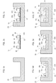
- Figures 1a-1f , 2a-2f , 3a-3f , and 4a-4f are schematic views illustrating embodiments of methods for producing a lighting device.
- Figures 1a-1f schematically represent an embodiment of a method for producing a strip-shaped lighting device, elongated in a longitudinal direction, perpendicular to the representation plane of the figures.
- reference 10 indicates an uncoated strip-shaped lighting module.
- the lighting module 10 may comprise a flexible printed circuit 12 elongated in a longitudinal direction perpendicular to the representation plane of the figure.
- the lighting module 10 can have an indefinite length in its longitudinal direction and may be provided in the form of a reel.
- the lighting module 10 may comprise a plurality of electrically-powered light radiation sources 16, which may be constituted by solid-state light radiation sources, for example, LEDs.
- the light radiation sources 16 may have respective light emission ends 16a.
- the printed circuit 12 may carry a plurality of electronic components 18 for powering and/or driving the light radiation sources 16.
- the light radiation sources 16 and the electronic components 18 may protrude from a first face 12a of the printed circuit 12.
- the light radiation sources 16 and the electronic components 18 may be fixed to the printed circuit 12 by surface-mount technology.
- the electronic components 18 may have a greater height than the light radiation sources 16, so that upper portions 18a of the electronic components 18 may protrude from the first face 12a of the printed circuit 12 by a greater height than the light emission ends 16a of the light radiation sources 16.
- Figure 1a shows a channel-shaped profile 20 for receiving the lighting module 10.
- the channel-shaped profile 20 may have a flexible plastic material profile.
- the channel-shaped profile 20 may have an indefinite length in its longitudinal direction and may be provided wound in a reel.
- the channel-shaped profile 20 may form a housing of the lighting device.
- the lighting module 10 may be arranged inside the channel-shaped profile 20, with the first face 12a carrying the light radiation sources 16 and the electronic components 18 facing upwards, and with a second face opposite the first face 12a resting on a bottom wall of the channel-shaped profile 20.
- the printed circuit 12 may be fixed to the channel-shaped profile 20 by means of a layer of glue, for example, by means of a "lamination" operation.
- a first opaque curable polymeric material 22 is dispensed inside the channel-shaped profile 20.
- the first opaque curable polymeric material 22 covers the printed circuit 12 and leaves the light emitting ends 16a of the light radiation sources 16 and the upper portions 18a of the electronic components 18 uncovered.
- the first opaque curable polymeric material 22 can be white silicone.
- the upper portions 18a of the electronic components 18 that protrude above the layer formed by the first curable polymeric material 22 may be covered with an opaque material.
- the opaque coating of the upper portions 18a of the electronic components 18 may be obtained by dispensing a second opaque curable polymeric material 24 onto the upper portions 18a of the electronic components 18.
- the second opaque polymeric material 24 may have a viscosity of more than 20,000 mPa*s.
- the second curable polymeric material 24 may form a layer with a thickness ranging from 100-500 ⁇ m on the upper portions 18a of the electronic components 18.
- the second opaque curable polymeric material 24 may have the same color as the first opaque curable polymeric material 22.
- a transparent curable polymeric material 26 can be dispensed into the channel-shaped profile 20, which forms an encapsulation layer covering the lighting module 10.
- the curable polymeric materials 22, 24, 26 may be cross-linked together, for example, by continuously passing the channel-shaped profile 20 containing the lighting module 10 coated by the first, the second and the third curable polymeric material 22, 24, 26 through a heating unit.
- the second opaque curable polymeric material 22 may be selectively dispensed, so as to only cover the upper portions 18a of the electronic components 18.
- the selective dispensing of the second curable polymeric material 22 is schematically represented in Figure 1e .
- a number of dispensing nozzles may be provided, in order to cover different areas of the printed circuit 12.
- the second curable polymeric material 22 can be continuously dispensed to cover areas of the lighting module 10 where the electronic components 18 are applied.
- the continuous dispensing of the second curable polymeric material 24 is schematically represented in Figure 2e .
- the remaining steps of the method can be the same as previously described in relation to the embodiment illustrated in Figures 1a-1f .
- the corresponding elements are indicated with the same numerical references.
- the electronic components 18 may be assembled in pre-established areas of the printed circuit 12, along which the second curable polymeric material 24 is dispensed.
- the electronic components 18 can be assembled along the longitudinal edges of the printed circuit 12.
- the second curable polymeric material 24 may have a sufficiently high viscosity, so as not to flow above the light-emitting ends 16a of the light radiation sources 16.
- the load of white pigments contained in the second curable polymeric material 24 can be increased to about twice the load of white pigments contained in the first curable polymeric material 22 in order to obtain a better coverage of the electronic components 18.
- the dispensing of the second curable polymeric material 24 can be carried out after the dispensing of the first curable polymeric material 22.
- coating the upper portions 18a of the electronic components 18 with an opaque material may include applying a coating of opaque material by pad printing.
- a pad printing head 28 may be provided, which applies a printed coating 30 on the upper portions 18a of the electronic components 18.
- the pad printing that applies the coating 30 to the electronic components 18 can be carried out on the uncoated lighting module 10 before placing the lighting module 10 inside the channel-shaped profile 20.
- the lighting module 10 can be positioned inside the channel-shaped profile 20 and, subsequently, the first curable polymeric material 22 can be dispensed onto the lighting module 10, leaving the light emitting ends 16a of the light radiation sources 16 uncovered and the upper portions 18a of the electronic components 18 precoated with the pad printing.
- a transparent curable polymeric material 26 can be dispensed within the channel-shaped profile 20 for sealing the lighting module 10.
- the coating of the upper portions 18a of the electronic components 18 by means of pad printing allows a flexible positioning of the electronic components 18 on the printed circuit 12.
- the pad printing may form a coating with a thin covering layer. If necessary, a double printing step can be provided to increase the thickness of the covering layer 30.
- the coating layer 30, applied by means of pad printing may have the same color as the first opaque curable polymeric material 22 (e.g. white) that covers the printed circuit 12 and the lower parts of the light radiation sources 16 and the electronic components 18.
- coating the upper portions 18a of the electronic components 18 with an opaque material may comprise applying opaque capsules 32 onto the upper portions 18a.
- the opaque capsules 32 may be pre-formed plastic capsules.
- the capsules 32 can be assembled on the upper portions 18a of the electronic components 18 by pick-and-place manipulators. Assembly of the capsules 32 on the upper portions 18a of the electronic components 18 can be carried out on the uncoated lighting module 10, before positioning the lighting module 10 inside the channel-shaped profile 20.
- the lighting module 10 comprising the capsules 32 applied to the upper portions 18a of the electronic components 18 can be arranged inside the channel-shaped profile 20 ( Figure 4d ) and, subsequently, the first curable polymeric material 22 can be dispensed within the channel-shaped profile 20 to cover the printed circuit 12 and the lower portions of the light radiation sources 16 and the electronic components 18 ( Figure 4e ). Then, a transparent curable polymeric material 26 can be dispensed into the channel-shaped profile 20 to seal the lighting module 10 ( Figure 4f ).
- the opaque capsules 32 may have the same color as the first curable polymeric material 22 (e.g. white).
- the dimensions of the opaque capsules 32 may depend on the components to be coated and the tolerances of the apparatus.
- One or more embodiments may, therefore, concern a method for producing a lighting device, which may comprise:
- coating said upper portions (e.g. 18a) of said electronic components (e.g. 18) with an opaque coating may comprise dispensing a second opaque curable polymeric material (e.g. 24) onto said upper portions (e.g. 18a) of said electronic components (e.g. 18).
- One or more embodiments may comprise selectively dispensing said second opaque curable polymeric material (e.g. 24) onto said upper portions (e.g. 18a) of said electronic components (e.g. 18).
- One or more embodiments may comprise continuously dispensing said second opaque curable polymeric material (e.g. 24) onto areas of said lighting module (e.g. 10) at which said electronic components are applied (e.g. 18).
- dispensing said second opaque curable polymeric material (e.g. 24) onto said upper portions (e.g. 18a) of said electronic components (e.g. 18) can be carried out after dispensing the first opaque curable polymeric material (22) into said channel-shaped profile (e.g. 20).
- said second opaque curable polymeric material (e.g. 24) may have a viscosity greater than 20,000 mPa*s.
- said second opaque curable polymeric material (e.g. 24) can form a coating with a thickness between 100-500 ⁇ m on said electronic components (e.g. 18).
- coating said upper portions (e.g. 18a) with an opaque coating may comprise applying said opaque coating (e.g. 30) to said upper portions (e.g. 18a) by pad printing.
- applying said opaque coating (e.g. 30) to said upper portions (e.g. 18a) by means of pad printing can be carried out before dispensing said first opaque curable polymeric material (e.g. 22) into said channel-shaped profile (e.g. 20).
- coating said upper portions (e.g. 18a) with an opaque coating may comprise applying opaque capsules (e.g. 32) onto said upper portions (e.g. 18a).
- applying said opaque capsules (e.g. 32) onto said upper portions (e.g. 18a) may be carried out before dispensing said first opaque curable polymeric material (e.g. 22) into said channel-shaped profile (e.g. 20).
- One or more embodiments may concern a lighting device, which may comprise:
- said opaque coating can be formed of a second opaque curable polymeric material (e.g. 24) dispensed onto said upper portions (e.g. 18a) of said electronic components (e.g. 18).
- said opaque coating e.g. 30
- said upper portions e.g. 18a
- said opaque coating can be formed by opaque capsules (e.g. 32) applied onto said upper portions (e.g. 18a).
Landscapes
- Engineering & Computer Science (AREA)
- General Engineering & Computer Science (AREA)
- Microelectronics & Electronic Packaging (AREA)
- Manufacturing & Machinery (AREA)
- Physics & Mathematics (AREA)
- Optics & Photonics (AREA)
- Non-Metallic Protective Coatings For Printed Circuits (AREA)
- Application Of Or Painting With Fluid Materials (AREA)
Abstract
- providing a strip-shaped lighting module (10) including a printed circuit (12) carrying a plurality of electrically-powered light radiation sources (16) having respective light emitting ends (16a) and a plurality of electronic components (18) protruding from a first face (12a) of said printed circuit (12), wherein said electronic components (18) have respective upper portions (18a) protruding from said printed circuit (12) beyond said light emitting ends (16a) of said electrically-powered light radiation sources (16),
- placing said lighting module (10) in a channel-shaped profile (20), with said first face (12a) of the printed circuit (12) facing upwards,
- dispensing a first opaque curable polymeric material (22) into said channel-shaped profile (20), in order to cover said printed circuit (12) and leave said light emitting ends (16a) of said electrically-powered light radiation sources (16) and said upper portions (18a) of said electronic components (18) uncovered, and
- coating said upper portions (18a) with an opaque coating (24, 30, 32).

Description
- The present description refers to lighting devices.
- One or more embodiments may refer to lighting devices that use solid-state light radiation sources, such as LED sources.
- One or more embodiments may concern a method for producing a lighting device.
- One or more embodiments may also concern a lighting device including a strip-shaped lighting module.
- In the field of lighting systems, the use of elongated lighting devices, for example strip-shaped, is widely used, and may comprise a printed circuit having the shape of a thin elongated strip on which a plurality of solid-state light radiation sources are fixed, for example LEDs, and a plurality of electronic components for powering and/or driving the light radiation sources.
- Lighting devices of this type may comprise an encapsulation layer of cross-linked polymeric material that covers the printed circuit and the electronic components for powering and/or driving the light radiation sources.
- In addition to technical requirements, such as, for example, high flexibility, ease of handling and shipping, and uniform light distribution, lighting devices can also be produced to meet aesthetic requirements. One of these aesthetic requirements may relate to the electronic components for powering and/or driving the light radiation sources. These electronic components may be dark in color, for example, black, and may appear as black dots when the lighting device is turned on, especially in the case in which the driving components are higher than the light radiation sources.
- In order to make the electronic components invisible, an opaque encapsulation layer, for example, white in color, may be dispensed onto the printed circuit and the electronic components, leaving the light emission ends of the light radiation sources above the opaque encapsulation layer exposed.
- This solution may be affected by some drawbacks, including:
- in order to leave only the light emission ends of the light radiation sources exposed, the electronic components should have a lower height than the light radiation sources,
- the laterally emitted light radiation would be blocked inside the opaque encapsulation layer, so that the selection of the light emission sources would be limited to greater light emission sources.
- One or more embodiments intend to contribute to overcoming the drawbacks outlined above.
- According to one or more embodiments, this object can be achieved by a method having the characteristics referred to in the following claims.
- One or more embodiments may also refer to a corresponding lighting device.
- The claims form an integral part of the technical disclosure provided here in relation to the invention.
- One or more embodiments may concern a method for producing a lighting device in which the electronic power supply and/or driving components are covered and the emission ends of the light radiation sources are exposed, even in the case in which the electronic power supply and driving components have a greater height than the light radiation sources.
- In one or more embodiments, the electronic power supply and/or driving components can be covered by an opaque curable polymeric material, which may be dispensed onto the electronic power supply and/or driving components in a selective or continuous manner.
- In one or more embodiments, the electronic power supply and/or driving components may be coated with a material applied by pad printing.
- In one or more embodiments, the electronic power supply and/or driving components may be covered by capsules, for example, applied by means of a pick-and-place manipulator.
- One or more embodiments may offer one or more of the following advantages:
- Possibility of integrating standard encapsulation techniques or standard pad printing methods into the process flow;
- Possibility of completely covering black electronic components without affecting the emission surfaces of the light radiation sources;
- Minor limitations in the choice of light emission sources, with consequent advantages in terms of lower costs and better availability of light radiation sources;
- Greater freedom in the selection of electronic components, with consequent advantages in terms of lower costs and better availability of electronic components;
- Better aesthetic appearance.
- One or more embodiments will be now described, purely by way of non-limiting example, with reference to the attached drawings, wherein:
Figures 1a-1f ,2a-2f ,3a-3f , and4a-4f are schematic views illustrating embodiments of methods for producing a lighting device. - It will be appreciated that, for clarity and simplicity of illustration, the various figures may not be reproduced on the same scale.
- In the following description, various specific details are illustrated aimed at a thorough understanding of examples of one or more embodiments. The embodiments can be implemented without one or more of the specific details, or with other methods, components, materials, etc. In other cases, known structures, materials or operations are not shown or described in detail to avoid obscuring various aspects of the embodiments. The reference to "an embodiment" in the context of this description indicates that a particular configuration, structure or characteristic described in relation to the embodiment is included in at least one embodiment. Therefore, phrases such as "in an embodiment", possibly present in different places of this description, do not necessarily refer to the same embodiment. Moreover, particular conformations, structures or characteristics can be combined in a suitable manner in one or more embodiments and/or associated with the embodiments in a different way from that illustrated here, so that, for example, a characteristic here exemplified in relation to a figure may be applied to one or more embodiments exemplified in a different figure.
- The references used here are only for convenience and do not, therefore, define the field of protection or the scope of the embodiments.
-
Figures 1a-1f schematically represent an embodiment of a method for producing a strip-shaped lighting device, elongated in a longitudinal direction, perpendicular to the representation plane of the figures. - In
Figure 1b ,reference 10 indicates an uncoated strip-shaped lighting module. Thelighting module 10 may comprise a flexible printedcircuit 12 elongated in a longitudinal direction perpendicular to the representation plane of the figure. Thelighting module 10 can have an indefinite length in its longitudinal direction and may be provided in the form of a reel. - The
lighting module 10 may comprise a plurality of electrically-poweredlight radiation sources 16, which may be constituted by solid-state light radiation sources, for example, LEDs. Thelight radiation sources 16 may have respective light emission ends 16a. Theprinted circuit 12 may carry a plurality ofelectronic components 18 for powering and/or driving thelight radiation sources 16. Thelight radiation sources 16 and theelectronic components 18 may protrude from afirst face 12a of theprinted circuit 12. Thelight radiation sources 16 and theelectronic components 18 may be fixed to the printedcircuit 12 by surface-mount technology. - In one or more embodiments, the
electronic components 18 may have a greater height than thelight radiation sources 16, so thatupper portions 18a of theelectronic components 18 may protrude from thefirst face 12a of the printedcircuit 12 by a greater height than the light emission ends 16a of thelight radiation sources 16. -
Figure 1a shows a channel-shaped profile 20 for receiving thelighting module 10. In one or more embodiments, the channel-shaped profile 20 may have a flexible plastic material profile. The channel-shaped profile 20 may have an indefinite length in its longitudinal direction and may be provided wound in a reel. In one or more embodiments, the channel-shaped profile 20 may form a housing of the lighting device. - As illustrated in
Figure 1c , in one or more embodiments thelighting module 10 may be arranged inside the channel-shaped profile 20, with thefirst face 12a carrying thelight radiation sources 16 and theelectronic components 18 facing upwards, and with a second face opposite thefirst face 12a resting on a bottom wall of the channel-shaped profile 20. - In one or more embodiments, the
printed circuit 12 may be fixed to the channel-shaped profile 20 by means of a layer of glue, for example, by means of a "lamination" operation. - With reference to
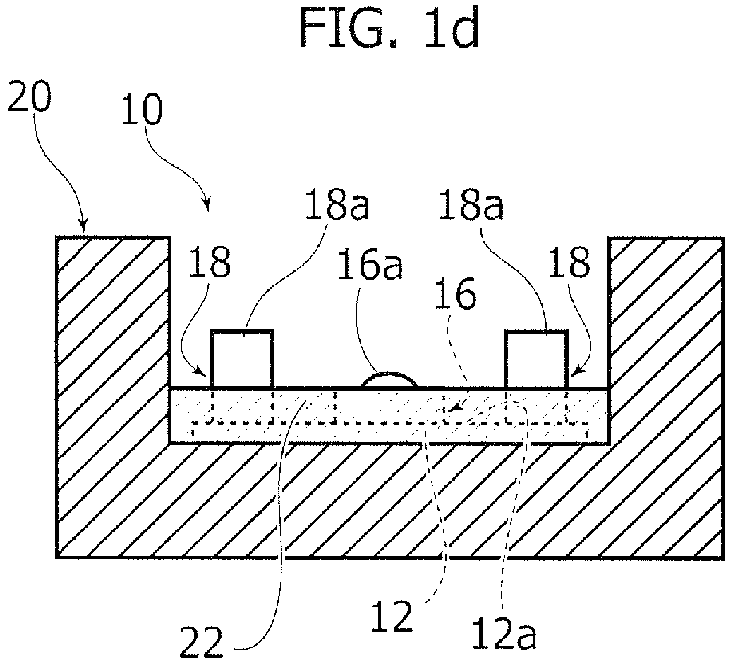
Figure 1d , in one or more embodiments, a first opaque curablepolymeric material 22 is dispensed inside the channel-shaped profile 20. In one or more embodiments, the first opaque curablepolymeric material 22 covers the printedcircuit 12 and leaves thelight emitting ends 16a of thelight radiation sources 16 and theupper portions 18a of theelectronic components 18 uncovered. In one or more embodiments, the first opaque curablepolymeric material 22 can be white silicone. - As illustrated in
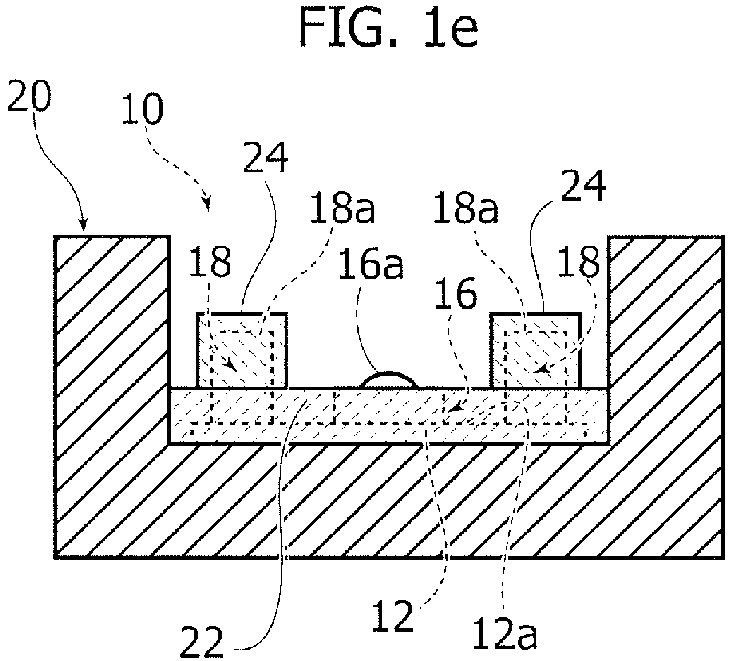
Figure 1e , theupper portions 18a of theelectronic components 18 that protrude above the layer formed by the first curablepolymeric material 22 may be covered with an opaque material. - In one or more embodiments, as illustrated in
Figure 1e , the opaque coating of theupper portions 18a of theelectronic components 18 may be obtained by dispensing a second opaque curablepolymeric material 24 onto theupper portions 18a of theelectronic components 18. In one or more embodiments, the second opaquepolymeric material 24 may have a viscosity of more than 20,000 mPa*s. In one or more embodiments, the second curablepolymeric material 24 may form a layer with a thickness ranging from 100-500 µm on theupper portions 18a of theelectronic components 18. The second opaque curablepolymeric material 24 may have the same color as the first opaque curablepolymeric material 22. - As illustrated in
Figure 1f , after dispensing the second opaque curablepolymeric material 24, a transparent curablepolymeric material 26 can be dispensed into the channel-shapedprofile 20, which forms an encapsulation layer covering thelighting module 10. - In one or more embodiments, the curable
polymeric materials profile 20 containing thelighting module 10 coated by the first, the second and the thirdcurable polymeric material - In one or more embodiments, the second opaque curable
polymeric material 22 may be selectively dispensed, so as to only cover theupper portions 18a of theelectronic components 18. The selective dispensing of the secondcurable polymeric material 22 is schematically represented inFigure 1e . To carry out the selective dispensing of the secondcurable polymeric material 22, a number of dispensing nozzles may be provided, in order to cover different areas of the printedcircuit 12. - In one or more embodiments, as exemplified in the sequence of
Figures 2a-2f , the secondcurable polymeric material 22 can be continuously dispensed to cover areas of thelighting module 10 where theelectronic components 18 are applied. The continuous dispensing of the secondcurable polymeric material 24 is schematically represented inFigure 2e . In the variant ofFigures 2a-2f , the remaining steps of the method can be the same as previously described in relation to the embodiment illustrated inFigures 1a-1f . InFigures 1a-1f and 2a-2f , the corresponding elements are indicated with the same numerical references. In the embodiment illustrated inFigures 2a-2f , theelectronic components 18 may be assembled in pre-established areas of the printedcircuit 12, along which the secondcurable polymeric material 24 is dispensed. For example, in one or more embodiments, theelectronic components 18 can be assembled along the longitudinal edges of the printedcircuit 12. - In one or more embodiments, the second
curable polymeric material 24 may have a sufficiently high viscosity, so as not to flow above the light-emittingends 16a of the light radiation sources 16. - In one or more embodiments, the load of white pigments contained in the second
curable polymeric material 24 can be increased to about twice the load of white pigments contained in the firstcurable polymeric material 22 in order to obtain a better coverage of theelectronic components 18. - In one or more embodiments, as exemplified in the embodiments shown in
Figures 1a-1f and2a-2f , the dispensing of the secondcurable polymeric material 24 can be carried out after the dispensing of the firstcurable polymeric material 22. - With reference to
Figures 3a-3f , in one or more embodiments, coating theupper portions 18a of theelectronic components 18 with an opaque material may include applying a coating of opaque material by pad printing. As illustrated inFigure 3c , apad printing head 28 may be provided, which applies a printedcoating 30 on theupper portions 18a of theelectronic components 18. In one or more embodiments, the pad printing that applies thecoating 30 to theelectronic components 18 can be carried out on theuncoated lighting module 10 before placing thelighting module 10 inside the channel-shapedprofile 20. As illustrated inFigures 3c, 3d and 3e , after the pad printing, thelighting module 10 can be positioned inside the channel-shapedprofile 20 and, subsequently, the firstcurable polymeric material 22 can be dispensed onto thelighting module 10, leaving the light emitting ends 16a of thelight radiation sources 16 uncovered and theupper portions 18a of theelectronic components 18 precoated with the pad printing. In one or more embodiments, as exemplified inFigure 3f , a transparent curablepolymeric material 26 can be dispensed within the channel-shapedprofile 20 for sealing thelighting module 10. - The coating of the
upper portions 18a of theelectronic components 18 by means of pad printing allows a flexible positioning of theelectronic components 18 on the printedcircuit 12. The pad printing may form a coating with a thin covering layer. If necessary, a double printing step can be provided to increase the thickness of thecovering layer 30. Thecoating layer 30, applied by means of pad printing, may have the same color as the first opaque curable polymeric material 22 (e.g. white) that covers the printedcircuit 12 and the lower parts of thelight radiation sources 16 and theelectronic components 18. - With reference to
Figures 4a-4f , in one or more embodiments, coating theupper portions 18a of theelectronic components 18 with an opaque material may comprise applyingopaque capsules 32 onto theupper portions 18a. Theopaque capsules 32 may be pre-formed plastic capsules. Thecapsules 32 can be assembled on theupper portions 18a of theelectronic components 18 by pick-and-place manipulators. Assembly of thecapsules 32 on theupper portions 18a of theelectronic components 18 can be carried out on theuncoated lighting module 10, before positioning thelighting module 10 inside the channel-shapedprofile 20. As exemplified inFigures 4d, 4e and 4f , thelighting module 10 comprising thecapsules 32 applied to theupper portions 18a of theelectronic components 18 can be arranged inside the channel-shaped profile 20 (Figure 4d ) and, subsequently, the firstcurable polymeric material 22 can be dispensed within the channel-shapedprofile 20 to cover the printedcircuit 12 and the lower portions of thelight radiation sources 16 and the electronic components 18 (Figure 4e ). Then, a transparent curablepolymeric material 26 can be dispensed into the channel-shapedprofile 20 to seal the lighting module 10 (Figure 4f ). - The
opaque capsules 32 may have the same color as the first curable polymeric material 22 (e.g. white). The dimensions of theopaque capsules 32 may depend on the components to be coated and the tolerances of the apparatus. - One or more embodiments may, therefore, concern a method for producing a lighting device, which may comprise:
- providing a strip-shaped lighting module (e.g. 10) including a printed circuit (e.g. 12) carrying a plurality of electrically-powered light radiation sources (e.g. 16) having respective light emitting ends (e.g. 16a) and a plurality of electronic components (e.g. 18) protruding from a first face (e.g. 12a) of said printed circuit (e.g. 12), wherein said electronic components (e.g. 18) have respective upper portions (e.g. 18a) protruding from said printed circuit (e.g. 12) beyond said light emitting ends (e.g. 16a) of said electrically-powered light radiation sources (e.g. 16),
- placing said lighting module (e.g. 10) in a channel-shaped profile (e.g. 20), with said first face (e.g. 12a) of the printed circuit (e.g. 12) facing upwards,
- dispensing a first opaque curable polymeric material (e.g. 22) into said channel-shaped profile (e.g. 20), in order to cover said printed circuit (e.g. 12) and leave said light emitting ends (e.g. 16a) of said electrically-powered light radiation sources (e.g. 16) and said upper portions (e.g. 18a) of said electronic components (e.g. 18) uncovered, and
- coating said upper portions (e.g. 18a) with an opaque coating (24, 30, 32).
- In one or more embodiments, coating said upper portions (e.g. 18a) of said electronic components (e.g. 18) with an opaque coating may comprise dispensing a second opaque curable polymeric material (e.g. 24) onto said upper portions (e.g. 18a) of said electronic components (e.g. 18).
- One or more embodiments may comprise selectively dispensing said second opaque curable polymeric material (e.g. 24) onto said upper portions (e.g. 18a) of said electronic components (e.g. 18).
- One or more embodiments may comprise continuously dispensing said second opaque curable polymeric material (e.g. 24) onto areas of said lighting module (e.g. 10) at which said electronic components are applied (e.g. 18).
- In one or more embodiments, dispensing said second opaque curable polymeric material (e.g. 24) onto said upper portions (e.g. 18a) of said electronic components (e.g. 18) can be carried out after dispensing the first opaque curable polymeric material (22) into said channel-shaped profile (e.g. 20).
- In one or more embodiments, said second opaque curable polymeric material (e.g. 24) may have a viscosity greater than 20,000 mPa*s.
- In one or more embodiments, said second opaque curable polymeric material (e.g. 24) can form a coating with a thickness between 100-500 µm on said electronic components (e.g. 18).
- In one or more embodiments, coating said upper portions (e.g. 18a) with an opaque coating may comprise applying said opaque coating (e.g. 30) to said upper portions (e.g. 18a) by pad printing.
- In one or more embodiments, applying said opaque coating (e.g. 30) to said upper portions (e.g. 18a) by means of pad printing can be carried out before dispensing said first opaque curable polymeric material (e.g. 22) into said channel-shaped profile (e.g. 20).
- In one or more embodiments, coating said upper portions (e.g. 18a) with an opaque coating may comprise applying opaque capsules (e.g. 32) onto said upper portions (e.g. 18a).
- In one or more embodiments, applying said opaque capsules (e.g. 32) onto said upper portions (e.g. 18a) may be carried out before dispensing said first opaque curable polymeric material (e.g. 22) into said channel-shaped profile (e.g. 20).
- One or more embodiments may concern a lighting device, which may comprise:
- a strip-shaped lighting module (e.g. 10) including a printed circuit (e.g. 12) carrying a plurality of electrically-powered light radiation sources (e.g. 16) having respective light emitting ends (e.g. 16a) and a plurality of electronic components (e.g. 18) protruding from a first face (e.g. 12a) of said printed circuit (e.g. 12), wherein said electronic components (e.g. 18) have respective upper portions (e.g. 18a) protruding from said printed circuit (e.g. 12) beyond said light emitting ends (e.g. 16a) of said electrically-powered light radiation sources (e.g. 16),
- a channel-shaped profile (e.g. 20) in which said strip-shaped lighting module (e.g. 10) is inserted,
- a first opaque curable polymeric material (e.g. 22) dispensed into said channel-shaped profile (e.g. 20), which covers said printed circuit (e.g. 12) and leaves said light emitting ends (e.g. 16a) of said electrically-powered light radiation sources (e.g. 16) and said upper portions (e.g. 18a) of said electronic components (e.g. 18) uncovered, and
- an opaque coating (e.g. 24, 30, 32) that coats said upper portions (e.g. 18a) of said electronic components (e.g. 18).
- In one or more embodiments, said opaque coating can be formed of a second opaque curable polymeric material (e.g. 24) dispensed onto said upper portions (e.g. 18a) of said electronic components (e.g. 18).
- In one or more embodiments, said opaque coating (e.g. 30) can be applied to said upper portions (e.g. 18a) by pad printing.
- In one or more embodiments, said opaque coating (e.g. 30) can be formed by opaque capsules (e.g. 32) applied onto said upper portions (e.g. 18a).
- Of course, without prejudice to the underlying principles of the invention, the details of construction and the embodiments may vary, even significantly, with respect to those illustrated here, purely by way of non-limiting example, without departing from the scope of the invention.
- This field of protection is defined by the attached claims.
LIST OF REFERENCE SIGNS lighting module 10 flexible printed circuit 12 electrically-powered light radiation sources 16 electronic components 18 first face 12a upper portions 18a channel-shaped profile 20 first opaque curable polymeric material 22 second opaque curable polymeric material 24 a transparent curable polymeric material 26 pad printing head 28 printed coating 30 opaque capsules 32
Claims (15)
- A method for producing a lighting device, comprising:- providing a strip-shaped lighting module (10) including a printed circuit (12) carrying a plurality of electrically-powered light radiation sources (16) having respective light emitting ends (16a) and a plurality of electronic components (18) protruding from a first face (12a) of said printed circuit, wherein said electronic components (18) have respective upper portions (18a) protruding from said printed circuit (12) beyond said light emitting ends (16a) of said electrically-powered light radiation sources (16),- placing said lighting module (10) in a channel-shaped profile (20), with said first face (12a) of the printed circuit (12) facing upwards,- dispensing a first opaque curable polymeric material (22) into said channel-shaped profile (20), in order to cover said printed circuit (12) and leave said light emitting ends (16a) of said electrically-powered light radiation sources (16) and said upper portions (18a) of said electronic components (18) uncovered, and- coating said upper portions (18a) with an opaque coating (24, 30, 32).
- A method according to claim 1, wherein coating said upper portions (18a) of said electronic components (18) with an opaque coating comprises dispensing a second opaque curable polymeric material (24) onto said upper portions (18a) of said electronic components (18) .
- A method according to claim 2, comprising selectively dispensing said second opaque curable polymeric material (24) onto said upper portions (18a) of said electronic components (18).
- A method according to claim 1 or claim 2, comprising continuously dispensing said second opaque curable polymeric material (24) onto areas of said lighting module (10) at which said electronic components (18) are applied.
- A method according to any of claims 2-4, wherein dispensing said second opaque curable polymeric material (24) onto said upper portions (18a) of said electronic components (18) is carried out after dispensing the first opaque curable polymeric material (22) into said channel-shaped profile (20).
- A method according to any of claims 1-5, wherein said second opaque curable polymeric material (24) has a viscosity greater than 20,000 mPa*s.
- A method according to any of claims 1-6, wherein said second opaque curable polymeric material (24) forms a coating on said electronic components (18), which has a thickness between 100 and 500 µm.
- A method according to claim 1, wherein coating said upper portions (18a) with an opaque coating comprises applying said opaque coating (30) to said upper portions (18a) by pad printing.
- A method according to claim 8, wherein applying said opaque coating (30) to said upper portions (18a) by pad printing is carried out before dispensing said first opaque curable polymeric material (22) into said channel-shaped profile (20).
- A method according to claim 1, wherein coating said upper portions (18a) with an opaque coating comprises applying opaque caps (32) onto said upper portions (18a).
- A method according to claim 10, wherein applying said opaque caps (32) onto said upper portions (18a) is carried out before dispensing said first opaque curable polymeric material (22) into said channel-shaped profile (20).
- A lighting device, comprising:- a strip-shaped lighting module (10) including a printed circuit (12) carrying a plurality of electrically-powered light radiation sources (16) having respective light emitting ends (16a) and a plurality of electronic components (18) protruding from a first face (12a) of said printed circuit (12), wherein said electronic components (18) have respective upper portions (18a) protruding from said printed circuit (12) beyond said light emitting ends (16a) of said electrically-powered light radiation sources (16),- a channel-shaped profile (20) in which said strip-shaped lighting module (10) is inserted,- a first opaque curable polymeric material (22) dispensed into said channel-shaped profile (20), which covers said printed circuit (12) and leaves uncovered said light emitting ends (16a) of said electrically-powered light radiation sources (16) and said upper portions (18a) of said electronic components (18), and- an opaque coating (24, 30, 32) that coats said upper portions (18a) of said electronic components (18) .
- A lighting device according to claim 12, wherein said opaque coating is formed by a second opaque curable polymeric material (24) dispensed onto said upper portions (18a) of said electronic components (18) .
- A lighting device according to claim 12, wherein said opaque coating (30) is applied onto said upper portions (18a) by pad printing.
- A lighting device according to claim 12, wherein said opaque coating (30) is formed by opaque caps (32) applied onto said upper portions (18a).
Applications Claiming Priority (1)
| Application Number | Priority Date | Filing Date | Title |
|---|---|---|---|
| IT201700083584 | 2017-07-21 |
Publications (2)
| Publication Number | Publication Date |
|---|---|
| EP3431862A1 true EP3431862A1 (en) | 2019-01-23 |
| EP3431862B1 EP3431862B1 (en) | 2020-06-17 |
Family
ID=60451012
Family Applications (1)
| Application Number | Title | Priority Date | Filing Date |
|---|---|---|---|
| EP18178310.1A Active EP3431862B1 (en) | 2017-07-21 | 2018-06-18 | A method for manufacturing a lighting device and corresponding device |
Country Status (1)
| Country | Link |
|---|---|
| EP (1) | EP3431862B1 (en) |
Citations (7)
| Publication number | Priority date | Publication date | Assignee | Title |
|---|---|---|---|---|
| JP2000004075A (en) * | 1998-06-15 | 2000-01-07 | Sharp Corp | Electronic circuit board |
| DE102008013454A1 (en) * | 2008-03-10 | 2010-07-22 | Vossloh-Schwabe Optoelectronic Gmbh & Co. Kg | LED component for e.g. room lighting application, has translucent sealing compound e.g. polyurethane sealing compound, that completely covers strip-shaped flexible printed circuit board |
| DE102012222093A1 (en) * | 2012-12-03 | 2014-06-05 | Osram Gmbh | Lighting device e.g. LED module has conversion transparent protective cover which is covered on light-emitting surface in which translucent diffusing layer is arranged with translucent matrix material having scattering particles |
| EP2846085A1 (en) * | 2013-09-09 | 2015-03-11 | OSRAM GmbH | A lighting device and corresponding method |
| EP2892078A1 (en) * | 2013-12-30 | 2015-07-08 | OSRAM GmbH | A lighting device and corresponding method |
| US20170205065A1 (en) * | 2016-01-20 | 2017-07-20 | Osram Gmbh | Method of producing lighting devices and corresponding lighting device |
| EP3263983A1 (en) * | 2016-06-28 | 2018-01-03 | OSRAM GmbH | A method of producing lighting devices and corresponding device |
-
2018
- 2018-06-18 EP EP18178310.1A patent/EP3431862B1/en active Active
Patent Citations (7)
| Publication number | Priority date | Publication date | Assignee | Title |
|---|---|---|---|---|
| JP2000004075A (en) * | 1998-06-15 | 2000-01-07 | Sharp Corp | Electronic circuit board |
| DE102008013454A1 (en) * | 2008-03-10 | 2010-07-22 | Vossloh-Schwabe Optoelectronic Gmbh & Co. Kg | LED component for e.g. room lighting application, has translucent sealing compound e.g. polyurethane sealing compound, that completely covers strip-shaped flexible printed circuit board |
| DE102012222093A1 (en) * | 2012-12-03 | 2014-06-05 | Osram Gmbh | Lighting device e.g. LED module has conversion transparent protective cover which is covered on light-emitting surface in which translucent diffusing layer is arranged with translucent matrix material having scattering particles |
| EP2846085A1 (en) * | 2013-09-09 | 2015-03-11 | OSRAM GmbH | A lighting device and corresponding method |
| EP2892078A1 (en) * | 2013-12-30 | 2015-07-08 | OSRAM GmbH | A lighting device and corresponding method |
| US20170205065A1 (en) * | 2016-01-20 | 2017-07-20 | Osram Gmbh | Method of producing lighting devices and corresponding lighting device |
| EP3263983A1 (en) * | 2016-06-28 | 2018-01-03 | OSRAM GmbH | A method of producing lighting devices and corresponding device |
Also Published As
| Publication number | Publication date |
|---|---|
| EP3431862B1 (en) | 2020-06-17 |
Similar Documents
| Publication | Publication Date | Title |
|---|---|---|
| US9719672B1 (en) | Method and apparatus for light square assembly | |
| TW541851B (en) | The encapsulation structure, method, and apparatus for organic light-emitted diode (OLED) devices | |
| CN102308144B (en) | Lighting module | |
| US20200182417A1 (en) | Light-Emitting Diode Strip, Method for Producing a Light-Emitting Diode Tape, and Light-Emitting Diode Tape | |
| US20170263826A1 (en) | Method for Applying Phosphor to Light Emitting Diodes and Apparatus Thereof | |
| US20080087903A1 (en) | Method for producing a light emitting diode arrangement, and light emitting diode arrangement | |
| EP3383146B1 (en) | Lighting device with ip protection and multidirectional bending capability, and method for manufacturing the same | |
| US20150077970A1 (en) | Light source, a method of manufacturing the same, and a backlight unit having the same | |
| US9324928B2 (en) | Lighting device and corresponding method | |
| EP3179832B1 (en) | Planar light-emitting panel and elastic jacket | |
| JPWO2018003027A1 (en) | Display device and manufacturing method of display device | |
| TWI552329B (en) | Organic light emitting device connection method | |
| KR102417580B1 (en) | Light emitting device, light emitting module, manufacturing method for light emitting device and munufacturing method for light emitting module | |
| JP2007288200A (en) | Light emitting diode chip sealing structure and light emitting diode chip structure packaging method | |
| CN106463588B (en) | For manufacturing method, conversion element and the opto-electronic device of multiple conversion elements | |
| EP3431862B1 (en) | A method for manufacturing a lighting device and corresponding device | |
| US20150155427A1 (en) | Method of manufacturing lighting device | |
| CN109084216B (en) | Integrally-packaged type row unit based on stage-like structure | |
| KR100879045B1 (en) | How to assemble LED module and LED module | |
| CN106164579B (en) | A kind of lighting apparatus and manufacturing method | |
| US10276762B2 (en) | Optoelectronic component | |
| KR20180067447A (en) | Display module and manufacturing method thereof | |
| US9903998B2 (en) | Lighting device and corresponding method | |
| US12422113B1 (en) | Endcap and method for making luminaire with endcap | |
| US11092328B2 (en) | Lamp and method for assembling a lamp |
Legal Events
| Date | Code | Title | Description |
|---|---|---|---|
| PUAI | Public reference made under article 153(3) epc to a published international application that has entered the european phase |
Free format text: ORIGINAL CODE: 0009012 |
|
| STAA | Information on the status of an ep patent application or granted ep patent |
Free format text: STATUS: THE APPLICATION HAS BEEN PUBLISHED |
|
| AK | Designated contracting states |
Kind code of ref document: A1 Designated state(s): AL AT BE BG CH CY CZ DE DK EE ES FI FR GB GR HR HU IE IS IT LI LT LU LV MC MK MT NL NO PL PT RO RS SE SI SK SM TR |
|
| AX | Request for extension of the european patent |
Extension state: BA ME |
|
| STAA | Information on the status of an ep patent application or granted ep patent |
Free format text: STATUS: REQUEST FOR EXAMINATION WAS MADE |
|
| 17P | Request for examination filed |
Effective date: 20190701 |
|
| RBV | Designated contracting states (corrected) |
Designated state(s): AL AT BE BG CH CY CZ DE DK EE ES FI FR GB GR HR HU IE IS IT LI LT LU LV MC MK MT NL NO PL PT RO RS SE SI SK SM TR |
|
| RIC1 | Information provided on ipc code assigned before grant |
Ipc: H05K 3/28 20060101ALI20191203BHEP Ipc: F21V 31/04 20060101ALI20191203BHEP Ipc: F21V 23/00 20150101ALI20191203BHEP Ipc: F21Y 103/10 20160101ALN20191203BHEP Ipc: F21Y 115/10 20160101ALN20191203BHEP Ipc: F21S 4/22 20160101AFI20191203BHEP Ipc: F21K 9/90 20160101ALI20191203BHEP |
|
| GRAP | Despatch of communication of intention to grant a patent |
Free format text: ORIGINAL CODE: EPIDOSNIGR1 |
|
| STAA | Information on the status of an ep patent application or granted ep patent |
Free format text: STATUS: GRANT OF PATENT IS INTENDED |
|
| RIC1 | Information provided on ipc code assigned before grant |
Ipc: F21Y 103/10 20160101ALN20191216BHEP Ipc: F21Y 115/10 20160101ALN20191216BHEP Ipc: F21K 9/90 20160101ALI20191216BHEP Ipc: F21S 4/22 20160101AFI20191216BHEP Ipc: H05K 3/28 20060101ALI20191216BHEP Ipc: F21V 23/00 20150101ALI20191216BHEP Ipc: F21V 31/04 20060101ALI20191216BHEP |
|
| INTG | Intention to grant announced |
Effective date: 20200120 |
|
| RIN1 | Information on inventor provided before grant (corrected) |
Inventor name: BISCARO, ALESSANDRO Inventor name: REISS, MARTIN Inventor name: BALDO, LORENZO Inventor name: RIEGER, THOMAS Inventor name: DIDONE', ROBERTO |
|
| GRAS | Grant fee paid |
Free format text: ORIGINAL CODE: EPIDOSNIGR3 |
|
| GRAA | (expected) grant |
Free format text: ORIGINAL CODE: 0009210 |
|
| STAA | Information on the status of an ep patent application or granted ep patent |
Free format text: STATUS: THE PATENT HAS BEEN GRANTED |
|
| AK | Designated contracting states |
Kind code of ref document: B1 Designated state(s): AL AT BE BG CH CY CZ DE DK EE ES FI FR GB GR HR HU IE IS IT LI LT LU LV MC MK MT NL NO PL PT RO RS SE SI SK SM TR |
|
| REG | Reference to a national code |
Ref country code: GB Ref legal event code: FG4D |
|
| REG | Reference to a national code |
Ref country code: CH Ref legal event code: EP |
|
| REG | Reference to a national code |
Ref country code: DE Ref legal event code: R096 Ref document number: 602018005289 Country of ref document: DE |
|
| REG | Reference to a national code |
Ref country code: IE Ref legal event code: FG4D |
|
| REG | Reference to a national code |
Ref country code: AT Ref legal event code: REF Ref document number: 1281744 Country of ref document: AT Kind code of ref document: T Effective date: 20200715 |
|
| RAP2 | Party data changed (patent owner data changed or rights of a patent transferred) |
Owner name: OSRAM GMBH Owner name: OSRAM S.P.A. - SOCIETA' RIUNITE OSRAM EDISON CLERICI |
|
| PG25 | Lapsed in a contracting state [announced via postgrant information from national office to epo] |
Ref country code: SE Free format text: LAPSE BECAUSE OF FAILURE TO SUBMIT A TRANSLATION OF THE DESCRIPTION OR TO PAY THE FEE WITHIN THE PRESCRIBED TIME-LIMIT Effective date: 20200617 Ref country code: LT Free format text: LAPSE BECAUSE OF FAILURE TO SUBMIT A TRANSLATION OF THE DESCRIPTION OR TO PAY THE FEE WITHIN THE PRESCRIBED TIME-LIMIT Effective date: 20200617 Ref country code: GR Free format text: LAPSE BECAUSE OF FAILURE TO SUBMIT A TRANSLATION OF THE DESCRIPTION OR TO PAY THE FEE WITHIN THE PRESCRIBED TIME-LIMIT Effective date: 20200918 Ref country code: FI Free format text: LAPSE BECAUSE OF FAILURE TO SUBMIT A TRANSLATION OF THE DESCRIPTION OR TO PAY THE FEE WITHIN THE PRESCRIBED TIME-LIMIT Effective date: 20200617 Ref country code: NO Free format text: LAPSE BECAUSE OF FAILURE TO SUBMIT A TRANSLATION OF THE DESCRIPTION OR TO PAY THE FEE WITHIN THE PRESCRIBED TIME-LIMIT Effective date: 20200917 |
|
| REG | Reference to a national code |
Ref country code: LT Ref legal event code: MG4D |
|
| REG | Reference to a national code |
Ref country code: NL Ref legal event code: MP Effective date: 20200617 |
|
| PG25 | Lapsed in a contracting state [announced via postgrant information from national office to epo] |
Ref country code: LV Free format text: LAPSE BECAUSE OF FAILURE TO SUBMIT A TRANSLATION OF THE DESCRIPTION OR TO PAY THE FEE WITHIN THE PRESCRIBED TIME-LIMIT Effective date: 20200617 Ref country code: HR Free format text: LAPSE BECAUSE OF FAILURE TO SUBMIT A TRANSLATION OF THE DESCRIPTION OR TO PAY THE FEE WITHIN THE PRESCRIBED TIME-LIMIT Effective date: 20200617 Ref country code: RS Free format text: LAPSE BECAUSE OF FAILURE TO SUBMIT A TRANSLATION OF THE DESCRIPTION OR TO PAY THE FEE WITHIN THE PRESCRIBED TIME-LIMIT Effective date: 20200617 Ref country code: BG Free format text: LAPSE BECAUSE OF FAILURE TO SUBMIT A TRANSLATION OF THE DESCRIPTION OR TO PAY THE FEE WITHIN THE PRESCRIBED TIME-LIMIT Effective date: 20200917 |
|
| REG | Reference to a national code |
Ref country code: AT Ref legal event code: MK05 Ref document number: 1281744 Country of ref document: AT Kind code of ref document: T Effective date: 20200617 |
|
| PG25 | Lapsed in a contracting state [announced via postgrant information from national office to epo] |
Ref country code: NL Free format text: LAPSE BECAUSE OF FAILURE TO SUBMIT A TRANSLATION OF THE DESCRIPTION OR TO PAY THE FEE WITHIN THE PRESCRIBED TIME-LIMIT Effective date: 20200617 Ref country code: AL Free format text: LAPSE BECAUSE OF FAILURE TO SUBMIT A TRANSLATION OF THE DESCRIPTION OR TO PAY THE FEE WITHIN THE PRESCRIBED TIME-LIMIT Effective date: 20200617 |
|
| PG25 | Lapsed in a contracting state [announced via postgrant information from national office to epo] |
Ref country code: CZ Free format text: LAPSE BECAUSE OF FAILURE TO SUBMIT A TRANSLATION OF THE DESCRIPTION OR TO PAY THE FEE WITHIN THE PRESCRIBED TIME-LIMIT Effective date: 20200617 Ref country code: RO Free format text: LAPSE BECAUSE OF FAILURE TO SUBMIT A TRANSLATION OF THE DESCRIPTION OR TO PAY THE FEE WITHIN THE PRESCRIBED TIME-LIMIT Effective date: 20200617 Ref country code: PT Free format text: LAPSE BECAUSE OF FAILURE TO SUBMIT A TRANSLATION OF THE DESCRIPTION OR TO PAY THE FEE WITHIN THE PRESCRIBED TIME-LIMIT Effective date: 20201019 Ref country code: ES Free format text: LAPSE BECAUSE OF FAILURE TO SUBMIT A TRANSLATION OF THE DESCRIPTION OR TO PAY THE FEE WITHIN THE PRESCRIBED TIME-LIMIT Effective date: 20200617 Ref country code: EE Free format text: LAPSE BECAUSE OF FAILURE TO SUBMIT A TRANSLATION OF THE DESCRIPTION OR TO PAY THE FEE WITHIN THE PRESCRIBED TIME-LIMIT Effective date: 20200617 Ref country code: AT Free format text: LAPSE BECAUSE OF FAILURE TO SUBMIT A TRANSLATION OF THE DESCRIPTION OR TO PAY THE FEE WITHIN THE PRESCRIBED TIME-LIMIT Effective date: 20200617 Ref country code: SM Free format text: LAPSE BECAUSE OF FAILURE TO SUBMIT A TRANSLATION OF THE DESCRIPTION OR TO PAY THE FEE WITHIN THE PRESCRIBED TIME-LIMIT Effective date: 20200617 Ref country code: IT Free format text: LAPSE BECAUSE OF FAILURE TO SUBMIT A TRANSLATION OF THE DESCRIPTION OR TO PAY THE FEE WITHIN THE PRESCRIBED TIME-LIMIT Effective date: 20200617 |
|
| PG25 | Lapsed in a contracting state [announced via postgrant information from national office to epo] |
Ref country code: PL Free format text: LAPSE BECAUSE OF FAILURE TO SUBMIT A TRANSLATION OF THE DESCRIPTION OR TO PAY THE FEE WITHIN THE PRESCRIBED TIME-LIMIT Effective date: 20200617 Ref country code: SK Free format text: LAPSE BECAUSE OF FAILURE TO SUBMIT A TRANSLATION OF THE DESCRIPTION OR TO PAY THE FEE WITHIN THE PRESCRIBED TIME-LIMIT Effective date: 20200617 Ref country code: IS Free format text: LAPSE BECAUSE OF FAILURE TO SUBMIT A TRANSLATION OF THE DESCRIPTION OR TO PAY THE FEE WITHIN THE PRESCRIBED TIME-LIMIT Effective date: 20201017 |
|
| REG | Reference to a national code |
Ref country code: DE Ref legal event code: R097 Ref document number: 602018005289 Country of ref document: DE |
|
| PG25 | Lapsed in a contracting state [announced via postgrant information from national office to epo] |
Ref country code: MC Free format text: LAPSE BECAUSE OF FAILURE TO SUBMIT A TRANSLATION OF THE DESCRIPTION OR TO PAY THE FEE WITHIN THE PRESCRIBED TIME-LIMIT Effective date: 20200617 Ref country code: LU Free format text: LAPSE BECAUSE OF NON-PAYMENT OF DUE FEES Effective date: 20200618 |
|
| REG | Reference to a national code |
Ref country code: BE Ref legal event code: MM Effective date: 20200630 |
|
| PLBE | No opposition filed within time limit |
Free format text: ORIGINAL CODE: 0009261 |
|
| STAA | Information on the status of an ep patent application or granted ep patent |
Free format text: STATUS: NO OPPOSITION FILED WITHIN TIME LIMIT |
|
| PG25 | Lapsed in a contracting state [announced via postgrant information from national office to epo] |
Ref country code: DK Free format text: LAPSE BECAUSE OF FAILURE TO SUBMIT A TRANSLATION OF THE DESCRIPTION OR TO PAY THE FEE WITHIN THE PRESCRIBED TIME-LIMIT Effective date: 20200617 Ref country code: IE Free format text: LAPSE BECAUSE OF NON-PAYMENT OF DUE FEES Effective date: 20200618 |
|
| 26N | No opposition filed |
Effective date: 20210318 |
|
| PG25 | Lapsed in a contracting state [announced via postgrant information from national office to epo] |
Ref country code: BE Free format text: LAPSE BECAUSE OF NON-PAYMENT OF DUE FEES Effective date: 20200630 Ref country code: SI Free format text: LAPSE BECAUSE OF FAILURE TO SUBMIT A TRANSLATION OF THE DESCRIPTION OR TO PAY THE FEE WITHIN THE PRESCRIBED TIME-LIMIT Effective date: 20200617 |
|
| PG25 | Lapsed in a contracting state [announced via postgrant information from national office to epo] |
Ref country code: FR Free format text: LAPSE BECAUSE OF NON-PAYMENT OF DUE FEES Effective date: 20200817 |
|
| REG | Reference to a national code |
Ref country code: CH Ref legal event code: PL |
|
| PG25 | Lapsed in a contracting state [announced via postgrant information from national office to epo] |
Ref country code: LI Free format text: LAPSE BECAUSE OF NON-PAYMENT OF DUE FEES Effective date: 20210630 Ref country code: CH Free format text: LAPSE BECAUSE OF NON-PAYMENT OF DUE FEES Effective date: 20210630 |
|
| PG25 | Lapsed in a contracting state [announced via postgrant information from national office to epo] |
Ref country code: TR Free format text: LAPSE BECAUSE OF FAILURE TO SUBMIT A TRANSLATION OF THE DESCRIPTION OR TO PAY THE FEE WITHIN THE PRESCRIBED TIME-LIMIT Effective date: 20200617 Ref country code: MT Free format text: LAPSE BECAUSE OF FAILURE TO SUBMIT A TRANSLATION OF THE DESCRIPTION OR TO PAY THE FEE WITHIN THE PRESCRIBED TIME-LIMIT Effective date: 20200617 Ref country code: CY Free format text: LAPSE BECAUSE OF FAILURE TO SUBMIT A TRANSLATION OF THE DESCRIPTION OR TO PAY THE FEE WITHIN THE PRESCRIBED TIME-LIMIT Effective date: 20200617 |
|
| PG25 | Lapsed in a contracting state [announced via postgrant information from national office to epo] |
Ref country code: MK Free format text: LAPSE BECAUSE OF FAILURE TO SUBMIT A TRANSLATION OF THE DESCRIPTION OR TO PAY THE FEE WITHIN THE PRESCRIBED TIME-LIMIT Effective date: 20200617 |
|
| GBPC | Gb: european patent ceased through non-payment of renewal fee |
Effective date: 20220618 |
|
| PG25 | Lapsed in a contracting state [announced via postgrant information from national office to epo] |
Ref country code: GB Free format text: LAPSE BECAUSE OF NON-PAYMENT OF DUE FEES Effective date: 20220618 |
|
| REG | Reference to a national code |
Ref country code: DE Ref legal event code: R081 Ref document number: 602018005289 Country of ref document: DE Owner name: OPTOTRONIC GMBH, DE Free format text: FORMER OWNER: OSRAM GMBH, 80807 MUENCHEN, DE Ref country code: DE Ref legal event code: R081 Ref document number: 602018005289 Country of ref document: DE Owner name: INVENTRONICS GMBH, DE Free format text: FORMER OWNER: OSRAM GMBH, 80807 MUENCHEN, DE |
|
| PGFP | Annual fee paid to national office [announced via postgrant information from national office to epo] |
Ref country code: DE Payment date: 20230630 Year of fee payment: 6 |
|
| REG | Reference to a national code |
Ref country code: DE Ref legal event code: R081 Ref document number: 602018005289 Country of ref document: DE Owner name: INVENTRONICS GMBH, DE Free format text: FORMER OWNER: OPTOTRONIC GMBH, 85748 GARCHING, DE |
|
| REG | Reference to a national code |
Ref country code: DE Ref legal event code: R119 Ref document number: 602018005289 Country of ref document: DE |
|
| PG25 | Lapsed in a contracting state [announced via postgrant information from national office to epo] |
Ref country code: DE Free format text: LAPSE BECAUSE OF NON-PAYMENT OF DUE FEES Effective date: 20250101 |