EP3431629A1 - Compositions and methods using same for deposition of silicon-containing films - Google Patents
Compositions and methods using same for deposition of silicon-containing films Download PDFInfo
- Publication number
- EP3431629A1 EP3431629A1 EP18180454.3A EP18180454A EP3431629A1 EP 3431629 A1 EP3431629 A1 EP 3431629A1 EP 18180454 A EP18180454 A EP 18180454A EP 3431629 A1 EP3431629 A1 EP 3431629A1
- Authority
- EP
- European Patent Office
- Prior art keywords
- plasma
- silicon
- group
- branched
- linear
- Prior art date
- Legal status (The legal status is an assumption and is not a legal conclusion. Google has not performed a legal analysis and makes no representation as to the accuracy of the status listed.)
- Granted
Links
- 0 [*+]N1[*+]N([*+])[S+]N([*+])[*+]1 Chemical compound [*+]N1[*+]N([*+])[S+]N([*+])[*+]1 0.000 description 3
Images


Classifications
-
- C—CHEMISTRY; METALLURGY
- C23—COATING METALLIC MATERIAL; COATING MATERIAL WITH METALLIC MATERIAL; CHEMICAL SURFACE TREATMENT; DIFFUSION TREATMENT OF METALLIC MATERIAL; COATING BY VACUUM EVAPORATION, BY SPUTTERING, BY ION IMPLANTATION OR BY CHEMICAL VAPOUR DEPOSITION, IN GENERAL; INHIBITING CORROSION OF METALLIC MATERIAL OR INCRUSTATION IN GENERAL
- C23C—COATING METALLIC MATERIAL; COATING MATERIAL WITH METALLIC MATERIAL; SURFACE TREATMENT OF METALLIC MATERIAL BY DIFFUSION INTO THE SURFACE, BY CHEMICAL CONVERSION OR SUBSTITUTION; COATING BY VACUUM EVAPORATION, BY SPUTTERING, BY ION IMPLANTATION OR BY CHEMICAL VAPOUR DEPOSITION, IN GENERAL
- C23C16/00—Chemical coating by decomposition of gaseous compounds, without leaving reaction products of surface material in the coating, i.e. chemical vapour deposition [CVD] processes
- C23C16/22—Chemical coating by decomposition of gaseous compounds, without leaving reaction products of surface material in the coating, i.e. chemical vapour deposition [CVD] processes characterised by the deposition of inorganic material, other than metallic material
- C23C16/30—Deposition of compounds, mixtures or solid solutions, e.g. borides, carbides, nitrides
- C23C16/40—Oxides
- C23C16/401—Oxides containing silicon
-
- C—CHEMISTRY; METALLURGY
- C23—COATING METALLIC MATERIAL; COATING MATERIAL WITH METALLIC MATERIAL; CHEMICAL SURFACE TREATMENT; DIFFUSION TREATMENT OF METALLIC MATERIAL; COATING BY VACUUM EVAPORATION, BY SPUTTERING, BY ION IMPLANTATION OR BY CHEMICAL VAPOUR DEPOSITION, IN GENERAL; INHIBITING CORROSION OF METALLIC MATERIAL OR INCRUSTATION IN GENERAL
- C23C—COATING METALLIC MATERIAL; COATING MATERIAL WITH METALLIC MATERIAL; SURFACE TREATMENT OF METALLIC MATERIAL BY DIFFUSION INTO THE SURFACE, BY CHEMICAL CONVERSION OR SUBSTITUTION; COATING BY VACUUM EVAPORATION, BY SPUTTERING, BY ION IMPLANTATION OR BY CHEMICAL VAPOUR DEPOSITION, IN GENERAL
- C23C16/00—Chemical coating by decomposition of gaseous compounds, without leaving reaction products of surface material in the coating, i.e. chemical vapour deposition [CVD] processes
- C23C16/22—Chemical coating by decomposition of gaseous compounds, without leaving reaction products of surface material in the coating, i.e. chemical vapour deposition [CVD] processes characterised by the deposition of inorganic material, other than metallic material
- C23C16/30—Deposition of compounds, mixtures or solid solutions, e.g. borides, carbides, nitrides
- C23C16/34—Nitrides
- C23C16/345—Silicon nitride
-
- C—CHEMISTRY; METALLURGY
- C23—COATING METALLIC MATERIAL; COATING MATERIAL WITH METALLIC MATERIAL; CHEMICAL SURFACE TREATMENT; DIFFUSION TREATMENT OF METALLIC MATERIAL; COATING BY VACUUM EVAPORATION, BY SPUTTERING, BY ION IMPLANTATION OR BY CHEMICAL VAPOUR DEPOSITION, IN GENERAL; INHIBITING CORROSION OF METALLIC MATERIAL OR INCRUSTATION IN GENERAL
- C23C—COATING METALLIC MATERIAL; COATING MATERIAL WITH METALLIC MATERIAL; SURFACE TREATMENT OF METALLIC MATERIAL BY DIFFUSION INTO THE SURFACE, BY CHEMICAL CONVERSION OR SUBSTITUTION; COATING BY VACUUM EVAPORATION, BY SPUTTERING, BY ION IMPLANTATION OR BY CHEMICAL VAPOUR DEPOSITION, IN GENERAL
- C23C16/00—Chemical coating by decomposition of gaseous compounds, without leaving reaction products of surface material in the coating, i.e. chemical vapour deposition [CVD] processes
- C23C16/22—Chemical coating by decomposition of gaseous compounds, without leaving reaction products of surface material in the coating, i.e. chemical vapour deposition [CVD] processes characterised by the deposition of inorganic material, other than metallic material
- C23C16/30—Deposition of compounds, mixtures or solid solutions, e.g. borides, carbides, nitrides
- C23C16/36—Carbonitrides
-
- C—CHEMISTRY; METALLURGY
- C23—COATING METALLIC MATERIAL; COATING MATERIAL WITH METALLIC MATERIAL; CHEMICAL SURFACE TREATMENT; DIFFUSION TREATMENT OF METALLIC MATERIAL; COATING BY VACUUM EVAPORATION, BY SPUTTERING, BY ION IMPLANTATION OR BY CHEMICAL VAPOUR DEPOSITION, IN GENERAL; INHIBITING CORROSION OF METALLIC MATERIAL OR INCRUSTATION IN GENERAL
- C23C—COATING METALLIC MATERIAL; COATING MATERIAL WITH METALLIC MATERIAL; SURFACE TREATMENT OF METALLIC MATERIAL BY DIFFUSION INTO THE SURFACE, BY CHEMICAL CONVERSION OR SUBSTITUTION; COATING BY VACUUM EVAPORATION, BY SPUTTERING, BY ION IMPLANTATION OR BY CHEMICAL VAPOUR DEPOSITION, IN GENERAL
- C23C16/00—Chemical coating by decomposition of gaseous compounds, without leaving reaction products of surface material in the coating, i.e. chemical vapour deposition [CVD] processes
- C23C16/44—Chemical coating by decomposition of gaseous compounds, without leaving reaction products of surface material in the coating, i.e. chemical vapour deposition [CVD] processes characterised by the method of coating
- C23C16/455—Chemical coating by decomposition of gaseous compounds, without leaving reaction products of surface material in the coating, i.e. chemical vapour deposition [CVD] processes characterised by the method of coating characterised by the method used for introducing gases into reaction chamber or for modifying gas flows in reaction chamber
- C23C16/45523—Pulsed gas flow or change of composition over time
- C23C16/45525—Atomic layer deposition [ALD]
- C23C16/45527—Atomic layer deposition [ALD] characterized by the ALD cycle, e.g. different flows or temperatures during half-reactions, unusual pulsing sequence, use of precursor mixtures or auxiliary reactants or activations
- C23C16/45536—Use of plasma, radiation or electromagnetic fields
-
- C—CHEMISTRY; METALLURGY
- C23—COATING METALLIC MATERIAL; COATING MATERIAL WITH METALLIC MATERIAL; CHEMICAL SURFACE TREATMENT; DIFFUSION TREATMENT OF METALLIC MATERIAL; COATING BY VACUUM EVAPORATION, BY SPUTTERING, BY ION IMPLANTATION OR BY CHEMICAL VAPOUR DEPOSITION, IN GENERAL; INHIBITING CORROSION OF METALLIC MATERIAL OR INCRUSTATION IN GENERAL
- C23C—COATING METALLIC MATERIAL; COATING MATERIAL WITH METALLIC MATERIAL; SURFACE TREATMENT OF METALLIC MATERIAL BY DIFFUSION INTO THE SURFACE, BY CHEMICAL CONVERSION OR SUBSTITUTION; COATING BY VACUUM EVAPORATION, BY SPUTTERING, BY ION IMPLANTATION OR BY CHEMICAL VAPOUR DEPOSITION, IN GENERAL
- C23C16/00—Chemical coating by decomposition of gaseous compounds, without leaving reaction products of surface material in the coating, i.e. chemical vapour deposition [CVD] processes
- C23C16/44—Chemical coating by decomposition of gaseous compounds, without leaving reaction products of surface material in the coating, i.e. chemical vapour deposition [CVD] processes characterised by the method of coating
- C23C16/455—Chemical coating by decomposition of gaseous compounds, without leaving reaction products of surface material in the coating, i.e. chemical vapour deposition [CVD] processes characterised by the method of coating characterised by the method used for introducing gases into reaction chamber or for modifying gas flows in reaction chamber
- C23C16/45523—Pulsed gas flow or change of composition over time
- C23C16/45525—Atomic layer deposition [ALD]
- C23C16/45553—Atomic layer deposition [ALD] characterized by the use of precursors specially adapted for ALD
-
- C—CHEMISTRY; METALLURGY
- C23—COATING METALLIC MATERIAL; COATING MATERIAL WITH METALLIC MATERIAL; CHEMICAL SURFACE TREATMENT; DIFFUSION TREATMENT OF METALLIC MATERIAL; COATING BY VACUUM EVAPORATION, BY SPUTTERING, BY ION IMPLANTATION OR BY CHEMICAL VAPOUR DEPOSITION, IN GENERAL; INHIBITING CORROSION OF METALLIC MATERIAL OR INCRUSTATION IN GENERAL
- C23C—COATING METALLIC MATERIAL; COATING MATERIAL WITH METALLIC MATERIAL; SURFACE TREATMENT OF METALLIC MATERIAL BY DIFFUSION INTO THE SURFACE, BY CHEMICAL CONVERSION OR SUBSTITUTION; COATING BY VACUUM EVAPORATION, BY SPUTTERING, BY ION IMPLANTATION OR BY CHEMICAL VAPOUR DEPOSITION, IN GENERAL
- C23C16/00—Chemical coating by decomposition of gaseous compounds, without leaving reaction products of surface material in the coating, i.e. chemical vapour deposition [CVD] processes
- C23C16/44—Chemical coating by decomposition of gaseous compounds, without leaving reaction products of surface material in the coating, i.e. chemical vapour deposition [CVD] processes characterised by the method of coating
- C23C16/48—Chemical coating by decomposition of gaseous compounds, without leaving reaction products of surface material in the coating, i.e. chemical vapour deposition [CVD] processes characterised by the method of coating by irradiation, e.g. photolysis, radiolysis, particle radiation
-
- C—CHEMISTRY; METALLURGY
- C23—COATING METALLIC MATERIAL; COATING MATERIAL WITH METALLIC MATERIAL; CHEMICAL SURFACE TREATMENT; DIFFUSION TREATMENT OF METALLIC MATERIAL; COATING BY VACUUM EVAPORATION, BY SPUTTERING, BY ION IMPLANTATION OR BY CHEMICAL VAPOUR DEPOSITION, IN GENERAL; INHIBITING CORROSION OF METALLIC MATERIAL OR INCRUSTATION IN GENERAL
- C23C—COATING METALLIC MATERIAL; COATING MATERIAL WITH METALLIC MATERIAL; SURFACE TREATMENT OF METALLIC MATERIAL BY DIFFUSION INTO THE SURFACE, BY CHEMICAL CONVERSION OR SUBSTITUTION; COATING BY VACUUM EVAPORATION, BY SPUTTERING, BY ION IMPLANTATION OR BY CHEMICAL VAPOUR DEPOSITION, IN GENERAL
- C23C16/00—Chemical coating by decomposition of gaseous compounds, without leaving reaction products of surface material in the coating, i.e. chemical vapour deposition [CVD] processes
- C23C16/44—Chemical coating by decomposition of gaseous compounds, without leaving reaction products of surface material in the coating, i.e. chemical vapour deposition [CVD] processes characterised by the method of coating
- C23C16/50—Chemical coating by decomposition of gaseous compounds, without leaving reaction products of surface material in the coating, i.e. chemical vapour deposition [CVD] processes characterised by the method of coating using electric discharges
-
- H—ELECTRICITY
- H10—SEMICONDUCTOR DEVICES; ELECTRIC SOLID-STATE DEVICES NOT OTHERWISE PROVIDED FOR
- H10P—GENERIC PROCESSES OR APPARATUS FOR THE MANUFACTURE OR TREATMENT OF DEVICES COVERED BY CLASS H10
- H10P14/00—Formation of materials, e.g. in the shape of layers or pillars
- H10P14/60—Formation of materials, e.g. in the shape of layers or pillars of insulating materials
- H10P14/63—Formation of materials, e.g. in the shape of layers or pillars of insulating materials characterised by the formation processes
- H10P14/6326—Deposition processes
- H10P14/6328—Deposition from the gas or vapour phase
- H10P14/6334—Deposition from the gas or vapour phase using decomposition or reaction of gaseous or vapour phase compounds, i.e. chemical vapour deposition
-
- H—ELECTRICITY
- H10—SEMICONDUCTOR DEVICES; ELECTRIC SOLID-STATE DEVICES NOT OTHERWISE PROVIDED FOR
- H10P—GENERIC PROCESSES OR APPARATUS FOR THE MANUFACTURE OR TREATMENT OF DEVICES COVERED BY CLASS H10
- H10P14/00—Formation of materials, e.g. in the shape of layers or pillars
- H10P14/60—Formation of materials, e.g. in the shape of layers or pillars of insulating materials
- H10P14/63—Formation of materials, e.g. in the shape of layers or pillars of insulating materials characterised by the formation processes
- H10P14/6326—Deposition processes
- H10P14/6328—Deposition from the gas or vapour phase
- H10P14/6334—Deposition from the gas or vapour phase using decomposition or reaction of gaseous or vapour phase compounds, i.e. chemical vapour deposition
- H10P14/6336—Deposition from the gas or vapour phase using decomposition or reaction of gaseous or vapour phase compounds, i.e. chemical vapour deposition in the presence of a plasma [PECVD]
-
- H—ELECTRICITY
- H10—SEMICONDUCTOR DEVICES; ELECTRIC SOLID-STATE DEVICES NOT OTHERWISE PROVIDED FOR
- H10P—GENERIC PROCESSES OR APPARATUS FOR THE MANUFACTURE OR TREATMENT OF DEVICES COVERED BY CLASS H10
- H10P14/00—Formation of materials, e.g. in the shape of layers or pillars
- H10P14/60—Formation of materials, e.g. in the shape of layers or pillars of insulating materials
- H10P14/63—Formation of materials, e.g. in the shape of layers or pillars of insulating materials characterised by the formation processes
- H10P14/6326—Deposition processes
- H10P14/6328—Deposition from the gas or vapour phase
- H10P14/6334—Deposition from the gas or vapour phase using decomposition or reaction of gaseous or vapour phase compounds, i.e. chemical vapour deposition
- H10P14/6339—Deposition from the gas or vapour phase using decomposition or reaction of gaseous or vapour phase compounds, i.e. chemical vapour deposition deposition by cyclic CVD, e.g. ALD, ALE or pulsed CVD
-
- H—ELECTRICITY
- H10—SEMICONDUCTOR DEVICES; ELECTRIC SOLID-STATE DEVICES NOT OTHERWISE PROVIDED FOR
- H10P—GENERIC PROCESSES OR APPARATUS FOR THE MANUFACTURE OR TREATMENT OF DEVICES COVERED BY CLASS H10
- H10P14/00—Formation of materials, e.g. in the shape of layers or pillars
- H10P14/60—Formation of materials, e.g. in the shape of layers or pillars of insulating materials
- H10P14/65—Formation of materials, e.g. in the shape of layers or pillars of insulating materials characterised by treatments performed before or after the formation of the materials
- H10P14/6516—Formation of materials, e.g. in the shape of layers or pillars of insulating materials characterised by treatments performed before or after the formation of the materials of treatments performed after formation of the materials
- H10P14/6518—Formation of materials, e.g. in the shape of layers or pillars of insulating materials characterised by treatments performed before or after the formation of the materials of treatments performed after formation of the materials by introduction of substances into an already-existing insulating layer
- H10P14/6519—Formation of materials, e.g. in the shape of layers or pillars of insulating materials characterised by treatments performed before or after the formation of the materials of treatments performed after formation of the materials by introduction of substances into an already-existing insulating layer the substance being oxygen
- H10P14/6522—Formation of materials, e.g. in the shape of layers or pillars of insulating materials characterised by treatments performed before or after the formation of the materials of treatments performed after formation of the materials by introduction of substances into an already-existing insulating layer the substance being oxygen introduced into a nitride material, e.g. changing SiN to SiON
-
- H—ELECTRICITY
- H10—SEMICONDUCTOR DEVICES; ELECTRIC SOLID-STATE DEVICES NOT OTHERWISE PROVIDED FOR
- H10P—GENERIC PROCESSES OR APPARATUS FOR THE MANUFACTURE OR TREATMENT OF DEVICES COVERED BY CLASS H10
- H10P14/00—Formation of materials, e.g. in the shape of layers or pillars
- H10P14/60—Formation of materials, e.g. in the shape of layers or pillars of insulating materials
- H10P14/65—Formation of materials, e.g. in the shape of layers or pillars of insulating materials characterised by treatments performed before or after the formation of the materials
- H10P14/6516—Formation of materials, e.g. in the shape of layers or pillars of insulating materials characterised by treatments performed before or after the formation of the materials of treatments performed after formation of the materials
- H10P14/6529—Formation of materials, e.g. in the shape of layers or pillars of insulating materials characterised by treatments performed before or after the formation of the materials of treatments performed after formation of the materials by exposure to a gas or vapour
-
- H—ELECTRICITY
- H10—SEMICONDUCTOR DEVICES; ELECTRIC SOLID-STATE DEVICES NOT OTHERWISE PROVIDED FOR
- H10P—GENERIC PROCESSES OR APPARATUS FOR THE MANUFACTURE OR TREATMENT OF DEVICES COVERED BY CLASS H10
- H10P14/00—Formation of materials, e.g. in the shape of layers or pillars
- H10P14/60—Formation of materials, e.g. in the shape of layers or pillars of insulating materials
- H10P14/65—Formation of materials, e.g. in the shape of layers or pillars of insulating materials characterised by treatments performed before or after the formation of the materials
- H10P14/6516—Formation of materials, e.g. in the shape of layers or pillars of insulating materials characterised by treatments performed before or after the formation of the materials of treatments performed after formation of the materials
- H10P14/6529—Formation of materials, e.g. in the shape of layers or pillars of insulating materials characterised by treatments performed before or after the formation of the materials of treatments performed after formation of the materials by exposure to a gas or vapour
- H10P14/6532—Formation of materials, e.g. in the shape of layers or pillars of insulating materials characterised by treatments performed before or after the formation of the materials of treatments performed after formation of the materials by exposure to a gas or vapour by exposure to a plasma
-
- H—ELECTRICITY
- H10—SEMICONDUCTOR DEVICES; ELECTRIC SOLID-STATE DEVICES NOT OTHERWISE PROVIDED FOR
- H10P—GENERIC PROCESSES OR APPARATUS FOR THE MANUFACTURE OR TREATMENT OF DEVICES COVERED BY CLASS H10
- H10P14/00—Formation of materials, e.g. in the shape of layers or pillars
- H10P14/60—Formation of materials, e.g. in the shape of layers or pillars of insulating materials
- H10P14/65—Formation of materials, e.g. in the shape of layers or pillars of insulating materials characterised by treatments performed before or after the formation of the materials
- H10P14/6516—Formation of materials, e.g. in the shape of layers or pillars of insulating materials characterised by treatments performed before or after the formation of the materials of treatments performed after formation of the materials
- H10P14/6536—Formation of materials, e.g. in the shape of layers or pillars of insulating materials characterised by treatments performed before or after the formation of the materials of treatments performed after formation of the materials by exposure to radiation, e.g. visible light
- H10P14/6538—Formation of materials, e.g. in the shape of layers or pillars of insulating materials characterised by treatments performed before or after the formation of the materials of treatments performed after formation of the materials by exposure to radiation, e.g. visible light by exposure to UV light
-
- H—ELECTRICITY
- H10—SEMICONDUCTOR DEVICES; ELECTRIC SOLID-STATE DEVICES NOT OTHERWISE PROVIDED FOR
- H10P—GENERIC PROCESSES OR APPARATUS FOR THE MANUFACTURE OR TREATMENT OF DEVICES COVERED BY CLASS H10
- H10P14/00—Formation of materials, e.g. in the shape of layers or pillars
- H10P14/60—Formation of materials, e.g. in the shape of layers or pillars of insulating materials
- H10P14/66—Formation of materials, e.g. in the shape of layers or pillars of insulating materials characterised by the type of materials
- H10P14/668—Formation of materials, e.g. in the shape of layers or pillars of insulating materials characterised by the type of materials the materials being characterised by the deposition precursor materials
- H10P14/6681—Formation of materials, e.g. in the shape of layers or pillars of insulating materials characterised by the type of materials the materials being characterised by the deposition precursor materials the precursor containing a compound comprising Si
-
- H—ELECTRICITY
- H10—SEMICONDUCTOR DEVICES; ELECTRIC SOLID-STATE DEVICES NOT OTHERWISE PROVIDED FOR
- H10P—GENERIC PROCESSES OR APPARATUS FOR THE MANUFACTURE OR TREATMENT OF DEVICES COVERED BY CLASS H10
- H10P14/00—Formation of materials, e.g. in the shape of layers or pillars
- H10P14/60—Formation of materials, e.g. in the shape of layers or pillars of insulating materials
- H10P14/66—Formation of materials, e.g. in the shape of layers or pillars of insulating materials characterised by the type of materials
- H10P14/668—Formation of materials, e.g. in the shape of layers or pillars of insulating materials characterised by the type of materials the materials being characterised by the deposition precursor materials
- H10P14/6681—Formation of materials, e.g. in the shape of layers or pillars of insulating materials characterised by the type of materials the materials being characterised by the deposition precursor materials the precursor containing a compound comprising Si
- H10P14/6682—Formation of materials, e.g. in the shape of layers or pillars of insulating materials characterised by the type of materials the materials being characterised by the deposition precursor materials the precursor containing a compound comprising Si the compound being a silane, e.g. disilane, methylsilane or chlorosilane
-
- H—ELECTRICITY
- H10—SEMICONDUCTOR DEVICES; ELECTRIC SOLID-STATE DEVICES NOT OTHERWISE PROVIDED FOR
- H10P—GENERIC PROCESSES OR APPARATUS FOR THE MANUFACTURE OR TREATMENT OF DEVICES COVERED BY CLASS H10
- H10P14/00—Formation of materials, e.g. in the shape of layers or pillars
- H10P14/60—Formation of materials, e.g. in the shape of layers or pillars of insulating materials
- H10P14/66—Formation of materials, e.g. in the shape of layers or pillars of insulating materials characterised by the type of materials
- H10P14/668—Formation of materials, e.g. in the shape of layers or pillars of insulating materials characterised by the type of materials the materials being characterised by the deposition precursor materials
- H10P14/6681—Formation of materials, e.g. in the shape of layers or pillars of insulating materials characterised by the type of materials the materials being characterised by the deposition precursor materials the precursor containing a compound comprising Si
- H10P14/6684—Formation of materials, e.g. in the shape of layers or pillars of insulating materials characterised by the type of materials the materials being characterised by the deposition precursor materials the precursor containing a compound comprising Si the compound comprising silicon and oxygen
- H10P14/6686—Formation of materials, e.g. in the shape of layers or pillars of insulating materials characterised by the type of materials the materials being characterised by the deposition precursor materials the precursor containing a compound comprising Si the compound comprising silicon and oxygen the compound being a molecule comprising at least one silicon-oxygen bond and the compound having hydrogen or an organic group attached to the silicon or oxygen, e.g. a siloxane
-
- H—ELECTRICITY
- H10—SEMICONDUCTOR DEVICES; ELECTRIC SOLID-STATE DEVICES NOT OTHERWISE PROVIDED FOR
- H10P—GENERIC PROCESSES OR APPARATUS FOR THE MANUFACTURE OR TREATMENT OF DEVICES COVERED BY CLASS H10
- H10P14/00—Formation of materials, e.g. in the shape of layers or pillars
- H10P14/60—Formation of materials, e.g. in the shape of layers or pillars of insulating materials
- H10P14/66—Formation of materials, e.g. in the shape of layers or pillars of insulating materials characterised by the type of materials
- H10P14/668—Formation of materials, e.g. in the shape of layers or pillars of insulating materials characterised by the type of materials the materials being characterised by the deposition precursor materials
- H10P14/6681—Formation of materials, e.g. in the shape of layers or pillars of insulating materials characterised by the type of materials the materials being characterised by the deposition precursor materials the precursor containing a compound comprising Si
- H10P14/6687—Formation of materials, e.g. in the shape of layers or pillars of insulating materials characterised by the type of materials the materials being characterised by the deposition precursor materials the precursor containing a compound comprising Si the compound comprising silicon and nitrogen
-
- H—ELECTRICITY
- H10—SEMICONDUCTOR DEVICES; ELECTRIC SOLID-STATE DEVICES NOT OTHERWISE PROVIDED FOR
- H10P—GENERIC PROCESSES OR APPARATUS FOR THE MANUFACTURE OR TREATMENT OF DEVICES COVERED BY CLASS H10
- H10P14/00—Formation of materials, e.g. in the shape of layers or pillars
- H10P14/60—Formation of materials, e.g. in the shape of layers or pillars of insulating materials
- H10P14/66—Formation of materials, e.g. in the shape of layers or pillars of insulating materials characterised by the type of materials
- H10P14/668—Formation of materials, e.g. in the shape of layers or pillars of insulating materials characterised by the type of materials the materials being characterised by the deposition precursor materials
- H10P14/6681—Formation of materials, e.g. in the shape of layers or pillars of insulating materials characterised by the type of materials the materials being characterised by the deposition precursor materials the precursor containing a compound comprising Si
- H10P14/6687—Formation of materials, e.g. in the shape of layers or pillars of insulating materials characterised by the type of materials the materials being characterised by the deposition precursor materials the precursor containing a compound comprising Si the compound comprising silicon and nitrogen
- H10P14/6689—Formation of materials, e.g. in the shape of layers or pillars of insulating materials characterised by the type of materials the materials being characterised by the deposition precursor materials the precursor containing a compound comprising Si the compound comprising silicon and nitrogen the compound being a silazane
-
- H—ELECTRICITY
- H10—SEMICONDUCTOR DEVICES; ELECTRIC SOLID-STATE DEVICES NOT OTHERWISE PROVIDED FOR
- H10P—GENERIC PROCESSES OR APPARATUS FOR THE MANUFACTURE OR TREATMENT OF DEVICES COVERED BY CLASS H10
- H10P14/00—Formation of materials, e.g. in the shape of layers or pillars
- H10P14/60—Formation of materials, e.g. in the shape of layers or pillars of insulating materials
- H10P14/69—Inorganic materials
- H10P14/692—Inorganic materials composed of oxides, glassy oxides or oxide-based glasses
- H10P14/6921—Inorganic materials composed of oxides, glassy oxides or oxide-based glasses containing silicon
- H10P14/69215—Inorganic materials composed of oxides, glassy oxides or oxide-based glasses containing silicon the material being a silicon oxide, e.g. SiO2
-
- H—ELECTRICITY
- H10—SEMICONDUCTOR DEVICES; ELECTRIC SOLID-STATE DEVICES NOT OTHERWISE PROVIDED FOR
- H10P—GENERIC PROCESSES OR APPARATUS FOR THE MANUFACTURE OR TREATMENT OF DEVICES COVERED BY CLASS H10
- H10P14/00—Formation of materials, e.g. in the shape of layers or pillars
- H10P14/60—Formation of materials, e.g. in the shape of layers or pillars of insulating materials
- H10P14/69—Inorganic materials
- H10P14/692—Inorganic materials composed of oxides, glassy oxides or oxide-based glasses
- H10P14/6921—Inorganic materials composed of oxides, glassy oxides or oxide-based glasses containing silicon
- H10P14/6922—Inorganic materials composed of oxides, glassy oxides or oxide-based glasses containing silicon the material containing Si, O and at least one of H, N, C, F or other non-metal elements, e.g. SiOC, SiOC:H or SiONC
Definitions
- compositions for forming a silicon-containing film in a plasma enhanced atomic layer deposition (PEALD) process are compositions for forming a silicon-containing film in a plasma enhanced atomic layer deposition (PEALD) process.
- PEALD plasma enhanced atomic layer deposition
- Exemplary silicon-containing films that can be deposited using the compositions and methods described herein include, without limitation, stoichiometric or non-stoichiometric, silicon nitride, silicon carbonitride, silicon oxynitride, silicon aluminum nitride, silicon oxide, and silicon carboxide films.
- Silicon nitride is often used as an insulator and chemical barrier in manufacturing integrated circuits, to electrically isolate different structures or as an etch mask in bulk micromachining. As a passivation layer for microchips, it is superior to silicon dioxide, as it is a significantly better diffusion barrier against water molecules and sodium ions, two major sources of corrosion and instability in microelectronics. It is also used as a dielectric between polysilicon layers in capacitors in analog chips.
- One of the commercial methods for forming silicon nitride or films employs dichlorosilane and ammonia as the precursor reactants.
- Low pressure chemical vapor deposition (LPCVD) using precursors such as dichlorosilane and ammonia require high deposition temperatures to get the best film properties. For example, temperatures greater than 750°C may be required to obtain reasonable growth rates and uniformities.
- Other processing issues involve the hazardous aspects of chlorine and chlorine byproducts.
- a silicon nitride film is considered a "high quality" film if it has one or more of the following characteristics: a density of 2.0 grams per cubic centimeter (g/cc) or greater, a low wet etch rate (as measured in dilute hydrofluoric acid (HF)), and combinations thereof compared to other silicon nitride films.
- the refractive index for the silicon nitride film should be 1.8 or greater.
- a low temperature e.g., processing temperature of about 500°C or less
- a method for depositing a conformal, high quality, silicon nitride film wherein the film has one or more of the following characteristics: a reflective index of 1.8 or higher, a density of 2.0 grams per cubic centimeter (g/cc) or greater, a low wet etch rate (as measured in dilute hydrofluoric acid (HF)), and combinations thereof compared to other silicon nitride films using other deposition methods or precursors.
- a reflective index of 1.8 or higher e.g., a density of 2.0 grams per cubic centimeter (g/cc) or greater
- a low wet etch rate as measured in dilute hydrofluoric acid (HF)
- the composition for depositing a silicon nitride film comprises: at least one silicon precursor compound selected from the group consisting of: wherein substituent R is independently selected from a hydrogen, a halide atom, a linear C 1 to C 10 alkyl group; a branched C 3 to C 10 alkyl group; a linear or branched C 3 to C 12 alkenyl group; a linear or branched C 3 to C 12 alkenyl group; a linear or branched C 3 to C 12 alkynyl group; a C 4 to C 10 cyclic alkyl group; and a C 6 to C 10 aryl group.
- substituent R is independently selected from a hydrogen, a halide atom, a linear C 1 to C 10 alkyl group; a branched C 3 to C 10 alkyl group; a linear or branched C 3 to C 12 alkenyl group; a linear or branched C 3 to C 12 alkynyl group; a C 4 to C
- a composition for forming a silicon-containing material comprising: (a) at least one silicon precursor compound selected from the group consisting of: wherein substituent R is independently selected from a hydrogen, a halide atom, a linear C 1 to C 10 alkyl group; a branched C 3 to C 10 alkyl group; a linear or branched C 3 to C 12 alkenyl group; a linear or branched C 3 to C 12 alkenyl group; a linear or branched C 3 to C 12 alkynyl group; a C 4 to C 10 cyclic alkyl group; and a C 6 to C 10 aryl group; and (b) a solvent, wherein the solvent has a boiling point and wherein the difference between the boiling point of the solvent and that of the at least one precursor compound is 40°C or less, and wherein the composition is substantially free of halide ions.
- exemplary solvent(s) can include, without limitation,
- a silicon nitride film comprising:
- silicon nitride refers to a film comprising silicon and nitrogen selected from the group consisting of stoichiometric or non-stoichiometric silicon nitride, silicon carbonitride, silicon carboxynitride, silicon aluminum nitride and there mixture thereof.
- a silicon nitride film is considered a "high quality" film if it has one or more of the following characteristics: a density of 2.0 grams per cubic centimeter (g/cc) or greater, a low wet etch rate (as measured in dilute hydrofluoric acid (HF)), and combinations thereof compared to other silicon nitride films.
- the refractive index for the silicon nitride film should be 1.8 or higher.
- described herein is composition for forming a silicon-containing film or material using silicon precursor compounds having Formulae IIA through IID.
- ALD atomic layer deposition
- ALD-like method that deposits a silicon nitride film at a low temperature, or one or more deposition temperatures ranging from about 20°C to about 500°C, using the Formula IIA through IID described herein in a plasma process which comprises nitrogen and optionally a noble or inert gas.
- Described herein are methods for forming a stoichiometric or non-stoichiometric silicon nitride film comprising silicon and nitrogen onto at least a portion of a substrate.
- the silicon nitride film may further comprise carbon. In certain embodiments, the silicon nitride film may further comprise aluminum such as a silicon aluminum nitride film. In certain embodiments, the silicon nitride film further comprises oxygen such as a silicon oxynitride film. In this or other embodiments, the silicon nitride film comprises oxygen and carbon such as a silicon carboxynitride film.
- the composition comprising at least one silicon precursor compound having Formulae IIA through IID may be used to deposit a silicon oxide material or film.
- silicon oxide refers to a film comprising silicon and nitrogen selected from the group consisting of stoichiometric or non-stoichiometric silicon oxide, carbon doped silicon oxide, silicon carboxynitride and mixtures thereof.
- the silicon nitride films described herein are deposited using at least one silicon precursor compound represented by Formulae IIA through IID below: wherein substituent R is independently selected from a hydrogen, a halide atom, a linear C 1 to C 10 alkyl group; a branched C 3 to C 10 alkyl group; a linear or branched C 3 to C 12 alkenyl group; a linear or branched C 3 to C 12 alkenyl group; a linear or branched C 3 to C 12 alkynyl group; a C 4 to C 10 cyclic alkyl group; and a C 6 to C 10 aryl group.
- substituent R is independently selected from a hydrogen, a halide atom, a linear C 1 to C 10 alkyl group; a branched C 3 to C 10 alkyl group; a linear or branched C 3 to C 12 alkenyl group; a linear or branched C 3 to C 12 alkenyl group; a linear or
- the silicon precursor compounds having three or more Si-N bonds, and optionally three or more Si-H 3 groups in Formula IIA, IIB and IID are more reactive towards at least a portion of the substrate surface, thus anchoring more silicon fragments on the surface during the deposition process. This in turn will increase the growth rate of the film as well as provide better surface coverage for substrate comprising surface features, such as without limitation, pores, trenches, and/or vias, thereby allowing for the deposition of a conformal silicon nitride or other silicon-containing film on the surface.
- An example of a Formula IIB compound is bis(disilylamino)silane (aka N,N'-disilyltrisilazane).
- Formula IIC compound is tris (ethylsillyl) amine.
- the silicon precursor compound is tris(ethylsillyl)amine, it is believed that the ethylene acts as leaving group in the deposition process thereby creating additional Si reactive sites while at the same time lowering the Si-H content in the precursor.
- linear alkyl denotes a linear functional group having from 1 to 10, 3 to 10, or 1 to 6 carbon atoms.
- exemplary linear alkyl groups include, but are not limited to, methyl, ethyl, propyl, butyl, pentyl, and hexyl groups.
- branched alkyl denotes a branched functional group having from 3 to 10, or 1 to 6 carbon atoms.
- Exemplary branched alkyl groups include, but are not limited to, isopropyl, isobutyl, sec-butyl, tert-butyl, iso-pentyl, tert-pentyl, isohexyl, and neohexyl.
- the alkyl group may have one or more functional groups such as, but not limited to, an alkoxy group, a dialkylamino group or combinations thereof, attached thereto. In other embodiments, the alkyl group does not have one or more functional groups attached thereto.
- the alkyl group may be saturated or, alternatively, unsaturated.
- halide denotes a chloride, bromide, iodide, or fluoride ion.
- cyclic alkyl denotes a cyclic group having from 3 to 10 or 5 to 10 atoms.
- exemplary cyclic alkyl groups include, but are not limited to, cyclobutyl, cyclopentyl, cyclohexyl, and cyclooctyl groups.
- the cyclic alkyl group may have one or more C 1 to C 10 linear, branched substituents, or substituents containing oxygen or nitrogen atoms.
- the cyclic alkyl group may have one or more linear or branched alkyls or alkoxy groups as substituents, such as, for example, a methylcyclohexyl group or a methoxycyclohexyl group.
- aryl denotes an aromatic cyclic functional group having from 3 to 10 carbon atoms, from 5 to 10 carbon atoms, or from 6 to 10 carbon atoms.
- exemplary aryl groups include, but are not limited to, phenyl, benzyl, chlorobenzyl, tolyl, and o-xylyl.
- alkenyl group denotes a group which has one or more carbon-carbon double bonds and has from 2 to 12, from 2 to 10, or from 2 to 6 carbon atoms.
- alkenyl groups include, but are not limited to, vinyl or allyl groups.
- alkynyl group denotes a group which has one or more carbon-carbon triple bonds and has from 2 to 12 or from 2 to 6 carbon atoms.
- the term "unsaturated” as used herein means that the functional group, substituent, ring or bridge has one or more carbon double or triple bonds.
- An example of an unsaturated ring can be, without limitation, an aromatic ring such as a phenyl ring.
- saturated means that the functional group, substituent, ring or bridge does not have one or more double or triple bonds.
- one or more of the alkyl group, alkenyl group, alkynyl group, alkoxysilylalkyl group, alkoxy group, aryloxy, aroyloxy, aryl group, and/or aromatic group in the formulae may be "substituted" or have one or more atoms or group of atoms substituted in place of, for example, a hydrogen atom.
- substituents include, but are not limited to, oxygen, sulfur, halogen atoms (e.g., F, CI, I, or Br), nitrogen, alkyl groups, and phosphorous.
- one or more of the alkyl group, alkenyl group, alkynyl group, alkoxyalkyl group, alkoxy group, alkylaminoalkyl group, aromatic and/or aryl group in the formulae may be unsubstituted.
- the method used to form the silicon-containing materials and films described herein are deposition processes.
- suitable deposition processes for the method disclosed herein include, but are not limited to, plasma enhanced ALD (PEALD) or plasma enhanced cyclic CVD (PECCVD) process.
- PEALD plasma enhanced ALD
- PECCVD plasma enhanced cyclic CVD
- the term “chemical vapor deposition processes” refers to any process wherein a substrate is exposed to one or more volatile precursors, which react and/or decompose on the substrate surface to produce the desired deposition.
- atomic layer deposition process refers to a self-limiting (e.g., the amount of film material deposited in each reaction cycle is constant), sequential surface chemistry that deposits silicon containing films of materials onto substrates of varying compositions.
- the precursors, reagents and sources used herein may be sometimes described as "gaseous", it is understood that the precursors can be either liquid or solid which are transported with or without an inert gas into the reactor via direct vaporization, bubbling or sublimation.
- the vaporized precursors can pass through a plasma generator.
- the silicon nitride film is deposited using a plasma enhanced ALD process.
- the silicon nitride film is deposited using a plasma enhanced CCVD process.
- reactor as used herein, includes without limitation, reaction chamber or deposition chamber.
- the ALD-like process is defined herein as a cyclic CVD process that provides a high conformal silicon nitride film such as, silicon nitride or silicon carbonitride on a substrate as shown by having at least one of the following: percentage of non-uniformity of about 5% or less as measured by ellipsometer, a deposition rate of 1 ⁇ or greater per cycle, or a combination thereof.
- the silicon precursor compounds having Formulae IIA through IID may be delivered to the reaction chamber such as a CVD or ALD reactor in a variety of ways.
- a liquid delivery system may be utilized.
- a combined liquid delivery and flash vaporization process unit may be employed, such as, for example, the turbo vaporizer manufactured by MSP Corporation of Shoreview, MN, to enable low volatility materials to be volumetrically delivered, which leads to reproducible transport and deposition without thermal decomposition of the precursor.
- the precursors described herein may be delivered in neat liquid form, or alternatively, may be employed in solvent formulations or compositions comprising same.
- the precursor formulations may include solvent component(s) of suitable character as may be desirable and advantageous in a given end use application to form a film on a substrate.
- a substrate having a surface to which at least a portion of silicon-containing film or materials is deposited thereupon is placed into a reactor deposition chamber.
- the temperature of the substrate may be controlled to be less than the walls of the reactor.
- the substrate temperature is held at a temperature from about room temperature (e.g., 20°C) to about 500°C.
- Alternative ranges for the substrate temperature have one or more of the following end points: 20, 50, 75, 100, 125, 150, 175, 200, 225, 250, 275, 300, 325, 350, 375, 400, 425, 450, 475, and 500°C.
- Exemplary temperature ranges include the following: 20 to 475°C, 100 to 400°C or 175 to 350°C.
- the one or more silicon-containing precursor compounds may be introduced into the reactor at a predetermined molar volume, or from about 0.1 to about 1000 micromoles.
- the silicon precursor or the silicon precursor comprising Formula IIA to IID and a solvent may be introduced into the reactor for a predetermined time period. In certain embodiments, the time period ranges from about 0.001 to about 500 seconds.
- the silicon-containing films comprise silicon nitride.
- the silicon-containing films deposited using the methods described herein are formed in the presence of nitrogen-containing source.
- a nitrogen-containing source may be introduced into the reactor in the form of at least one nitrogen-containing source and/or may be present incidentally in the other precursors used in the deposition process.
- Suitable nitrogen-containing source gases may include, for example, ammonia, hydrazine, monoalkylhydrazine, dialkylhydrazine, plasma comprising nitrogen, plasma comprising nitrogen and hydrogen, plasma comprising nitrogen and helium, plasma comprising nitrogen and argon, ammonia plasma, plasma comprising nitrogen and ammonia, plasma comprising ammonia and helium, plasma comprising ammonia and argon plasma, NF 3 plasma, organoamine plasma, and mixtures thereof.
- the plasma is selected from the group consisting of hydrogen plasma, helium plasma, neon plasma, argon plasma, xenon plasma, hydrogen/helium plasma, hydrogen/argon plasma and mixtures thereof.
- the nitrogen containing source is substantially free of (e.g., has 2 weight percent (wt. %) or less) hydrogen to avoid introducing additional hydrogen into the final silicon nitride film and is selected from the group consisting of nitrogen plasma, nitrogen/helium, nitrogen/argon plasma.
- the nitrogen containing source is selected from monoalkylhydrazine, dialkylhydrazine.
- the nitrogen containing source can be selected from the group consisting of organic amine plasma such as methylamine plasma, dimethylamine plasma, trimethylamine plasma, ethylamine plasma, diethylamine plasma, trimethylamine plasma, ethylenediamine plasma.
- organic amine as used herein describes organic compound has at least one nitrogen atom.
- examples of organic amine but are not limited to, methylamine, ethylamine, propylamine, iso-propylamine, tert-butylamine, sec-butylamine, tert-amylamine, ethylenediamine, dimethylamine, trimethylamine, diethylamine, pyrrole, 2,6-dimethylpiperidine, di-n-propylamine, di-iso-propylamine, ethylmethylamine, N-methylaniline, pyridine, triethylamine.
- organoamino group refers to an organic group consisting of at least one nitrogen atom derived from secondary or primary organoamines as described above. "Organoamino group” does not include -NH 2 group.
- the nitrogen-containing source is introduced into the reactor at a flow rate ranging from about 1 to about 2000 square cubic centimeters (sccm) or from about 1 to about 1000 sccm.
- the nitrogen-containing source can be introduced for a time that ranges from about 0.1 to about 100 seconds.
- the precursor pulse can have a pulse duration that is greater than 0.01 seconds, and the nitrogen-containing source can have a pulse duration that is less than 0.01 seconds.
- the purge duration between the pulses that can be as low as 0 seconds or is continuously pulsed without a purge in-between.
- the silicon-containing films deposited using the methods described herein are formed in the presence of oxygen using an oxygen-containing source, reagent or precursor comprising oxygen.
- An oxygen-containing source may be introduced into the reactor in the form of at least one oxygen-containing source.
- the oxygen-containing source may be present incidentally in the other precursors used in the deposition process.
- Suitable oxygen-containing source gases may include, for example, water (H 2 O) (e.g., deionized water, purifier water, and/or distilled water), oxygen (O 2 ), oxygen plasma, ozone (O 3 ), NO, N 2 O, NO 2 , carbon monoxide (CO), carbon dioxide (CO 2 ) and combinations thereof.
- the oxygen-containing source is introduced into the reactor at a flow rate ranging from about 1 to about 2000 square cubic centimeters (sccm) or from about 1 to about 1000 sccm.
- the oxygen-containing source can be introduced for a time that ranges from about 0.1 to about 100 seconds.
- the oxygen-containing source comprises water having a temperature of 10°C or greater.
- the precursor pulse can have a pulse duration that is greater than 0.01 seconds, and the oxygen-containing source can have a pulse duration that is less than 0.01 seconds, while the water pulse duration can have a pulse duration that is less than 0.01 seconds.
- the purge duration between the pulses that can be as low as 0 seconds or is continuously pulsed without a purge in-between.
- the oxygen-containing source or reagent is provided in a molecular amount less than a 1:1 ratio to the silicon precursor, so that at least some carbon is retained in the as deposited silicon-containing film.
- the temperature of the reactor in the introducing step is at one or more temperatures ranging from about room temperature (e.g., 20°C) to about 500°C.
- Alternative ranges for the substrate temperature have one or more of the following end points: 20, 50, 75, 100, 125, 150, 175, 200, 225, 250, 275, 300, 325, 350, 375, 400, 425, 450, 475, and 500°C.
- Exemplary temperature ranges include the following: 20 to 475°C, 100 to 400°C or 175 to 350°C.
- Energy is applied to the at least one of the precursor compound, nitrogen-containing source, oxygen-containing source, other reagents, or a combination thereof to induce reaction and to form the silicon-containing film or coating or a chemisorbed layer on at least a portion of the substrate.
- Such energy can be provided by, but not limited to, thermal, plasma, pulsed plasma, helicon plasma, high density plasma, inductively coupled plasma, X-ray, e-beam, photon, remote plasma methods, and combinations thereof.
- a secondary RF frequency source can be used to modify the plasma characteristics at the substrate surface.
- the plasma-generated process may comprise a direct plasma-generated process in which plasma is directly generated in the reactor, or alternatively a remote plasma-generated process in which plasma is generated outside of the reactor and supplied into the reactor.
- the plasma is generated at a power density ranging from about 0.01 to about 1.5 W/cm 2 .
- the deposition methods disclosed herein may involve one or more purge gases.
- the purge gas which is used to purge away unconsumed reactants and/or reaction byproducts, is an inert gas that does not react with the precursors.
- Exemplary purge gases include, but are not limited to, argon (Ar), nitrogen (N 2 ), helium (He), neon, hydrogen (H 2 ), and mixtures thereof.
- a purge gas is supplied into the reactor at a flow rate ranging from about 10 to about 2000 sccm for about 0.1 to 1000 seconds, thereby purging the unreacted material and any byproduct that may remain in the reactor.
- the respective step of supplying the precursors, oxygen-containing source, the nitrogen-containing source, and/or other precursors, source gases, and/or reagents may be performed by changing the time for supplying them to change the stoichiometric composition of the resultant film or material.
- a flow of argon and/or other gas may be employed as a carrier gas to help deliver the vapor of the at least one precursor compound to the reaction chamber during the precursor pulsing.
- the reaction chamber process pressure is about 10 Torr or less, 5 Torr or less, 2 Torr or less, 1 torr or less.
- a substrate is heated on a heater stage in a reaction chamber that is exposed to the precursor compound initially to allow the compound to chemically adsorb onto the surface of the substrate.
- a purge gas such as nitrogen, argon, or other inert gas purges away unabsorbed excess precursor compound from the process chamber.
- a nitrogen-containing source may be introduced into reaction chamber to react with the absorbed surface followed by another gas purge to remove reaction by-products from the chamber. The process cycle can be repeated to achieve the desired film thickness.
- pumping under vacuum can be used to remove unabsorbed excess precursor compound from the process chamber, after sufficient evacuation under pumping, a nitrogen-containing source may be introduced into reaction chamber to react with the absorbed surface followed by another pumping down purge to remove reaction by-products from the chamber.
- the precursor compound and the nitrogen-containing source can be co-flowed into reaction chamber to react on the substrate surface to deposit silicon nitride.
- the purge step is not used.
- the steps of the methods described herein may be performed in a variety of orders, may be performed sequentially or concurrently (e.g., during at least a portion of another step), and any combination thereof.
- the respective step of supplying the precursors and the nitrogen-containing source gases may be performed by varying the duration of the time for supplying them to change the stoichiometric composition of the resulting silicon-containing film.
- a silicon nitride film comprising the steps of:
- the silicon precursors described herein and compositions comprising the silicon precursors having three or more Si-N bonds, and optionally three or more Si-H 3 groups represented by Formulae IIA through IID, according to the present invention are preferably substantially free of halide ions such as chloride or metal ions such as Al.
- halide ions or halides
- the term "substantially free” as it relates to halide ions (or halides) such as, for example, chlorides and fluorides, bromides, iodides, Al 3+ ions, Fe 2+ , Fe 3+ , Ni 2+ , Cr 3+ means less than 5 ppm (by weight), preferably less than 3 ppm, and more preferably less than 1 ppm, and most preferably 0 ppm.
- Chlorides or metal ions are known to act as decomposition catalysts for silicon precursors. Significant levels of chloride in the final product can cause the silicon precursors to degrade. The gradual degradation of the silicon precursors may directly impact the film deposition process making it difficult for the semiconductor manufacturer to meet film specifications. In addition, the shelf-life or stability is negatively impacted by the higher degradation rate of the silicon precursors thereby making it difficult to guarantee a 1-2 year shelf-life. Moreover, silicon precursors are known to form flammable and/or pyrophoric gases upon decomposition such as hydrogen and silane. Therefore, the accelerated decomposition of the silicon precursors presents safety and performance concerns related to the formation of these flammable and/or pyrophoric gaseous byproducts.
- compositions according to the present invention that are substantially free of halides can be achieved by (1) reducing or eliminating chloride sources during chemical synthesis, and/or (2) implementing an effective purification process to remove chloride from the crude product such that the final purified product is substantially free of chlorides.
- Chloride sources may be reduced during synthesis by using reagents that do not contain halides such as chlorodislanes, bromodisilanes, or iododislanes thereby avoiding the production of by-products that contain halide ions.
- the aforementioned reagents should be substantially free of chloride impurities such that the resulting crude product is substantially free of chloride impurities.
- the synthesis should not use halide based solvents, catalysts, or solvents which contain unacceptably high levels of halide contamination.
- the crude product may also be treated by various purification methods to render the final product substantially free of halides such as chlorides. Such methods are well described in the prior art and, may include, but are not limited to purification processes such as distillation, or adsorption. Distillation is commonly used to separate impurities from the desire product by exploiting differences in boiling point. Adsorption may also be used to take advantage of the differential adsorptive properties of the components to effect separation such that the final product is substantially free of halide. Adsorbents such as, for example, commercially available MgO-Al 2 O 3 blends can be used to remove halides such as chloride.
- the solvent or mixture thereof selected does not react with the silicon precursors.
- the amount of solvent by weight percentage in the composition ranges from 0.5% by weight to 99.5% or from 10% by weight to 75%.
- the solvent has a boiling point (b.p.) similar to the b.p. of the silicon precursor precursors of Formula II or the difference between the b.p. of the solvent and the b.p. of the silicon precursor precursors of Formula II is 40°C or less, 30°C or less, or 20°C or less, 10°C or less, or 5°C or less.
- the difference between the boiling points ranges from any one or more of the following end-points: 0, 10, 20, 30, or 40°C.
- suitable ranges of b.p. difference include without limitation, 0 to 40°C, 20° to 30°C, or 10° to 30°C.
- suitable solvents in the compositions include, but are not limited to, an ether (such as 1,4-dioxane, dibutyl ether), a tertiary amine (such as pyridine, 1-methylpiperidine, 1-ethylpiperidine, N,N'-Dimethylpiperazine, N,N,N',N'-Tetramethylethylenediamine), a nitrile (such as benzonitrile), an alkyl hydrocarbon (such as octane, nonane, dodecane, ethylcyclohexane), an aromatic hydrocarbon (such as toluene, mesitylene), a tertiary aminoether (such as bis(2-dimethylaminoethyl) ether), or mixtures thereof.
- an ether such as 1,4-dioxane, dibutyl ether
- a tertiary amine such as pyridine, 1-methylpiperidine, 1-ethy
- compositions include, but not limited to, a composition comprising bis(disilylamino)silane (b.p. about 135°C) and octane (b.p. 125 to 126°C); a composition comprising bis(disilylamino)silane (b.p. about 135°C) and ethylcyclohexane (b.p. 130-132°C); a composition comprising bis(disilylamino)silane (b.p. about 135°C) and cyclooctane (b.p. 149°C); a composition comprising bis(disilylamino)silane (b.p. about 135°C), and toluene (b.p. 115°C).
- a vessel for depositing a silicon-containing film comprising one or more silicon precursor compound having Formulae IIA through IID comprises at least one pressurizable vessel (preferably of stainless steel) fitted with the proper valves and fittings to allow the delivery of one or more precursors to the reactor for a CVD or an ALD process.
- the silicon precursor compound is provided in a pressurizable vessel comprised of stainless steel and the purity of the silicon precursor is 98% by weight or greater or 99.5% or greater which is suitable for the majority of semiconductor applications.
- such vessels can also have means for mixing the precursors with one or more additional precursor if desired.
- the contents of the vessel(s) can be premixed with an additional precursor.
- the silicon precursor compounds described herein and/or other precursor can be maintained in separate vessels or in a single vessel having separation means for maintaining the silicon precursor having Formulae IIA through IID and other precursor separate during storage.
- the method described herein further comprises one or more additional silicon-containing precursors other than the silicon precursors having the above Formulae IIA through IID.
- additional silicon-containing precursors include, but are not limited to, monoaminosilane (e.g., di-iso-propylaminosilane, di-sec-butylaminosilane, phenylmethylaminosilane; organo-silicon compounds such as trisilylamine (TSA); monoaminosilane (di-iso-propylaminosilane, di-sec-butylaminosilane, phenylmethylaminosilane); siloxanes (e.g., hexamethyl disiloxane (HMDSO) and dimethyl siloxane (DMSO)); organosilanes (e.g., methylsilane, dimethylsilane, diethylsilane, vinyl trimethylsilane, trimethylsilane, tetramethylsilane, ethyl
- the silicon precursors having Formulae IIA through IID described herein can also be used as a dopant for metal containing films, such as but not limited to, metal oxide films or metal nitride films.
- the metal containing film is deposited using an ALD or CVD process such as those processes described herein using metal alkoxide, metal amide, or volatile organometallic precursors.
- suitable metal alkoxide precursors that may be used with the method disclosed herein include, but are not limited to, group 3 to 6 metal alkoxide, group 3 to 6 metal complexes having both alkoxy and alkyl substituted cyclopentadienyl ligands, group 3 to 6 metal complexes having both alkoxy and alkyl substituted pyrrolyl ligands, group 3 to 6 metal complexes having both alkoxy and diketonate ligands; group 3 to 6 metal complexes having both alkoxy and ketoester ligands;
- suitable metal amide precursors that may be used with the method disclosed herein include, but are not limited to, AlCl 3 , trimethylaluminum (TMA), triethylaluminum, methylaluminum chloride, tris(dimethylamino)aluminum (TDMAA), tris(dimethylamino)aluminum (TDMAA), and tris(diethylamino)a
- organometallic precursors that may be used with the method disclosed herein include, but are not limited to, group 3 metal cyclopentadienyls or alkyl cyclopentadienyls.
- exemplary Group 3 to 6 metal herein include, but not limited to, Y, La, Ce, Pr, Nd, Sm, Eu, Gd, Tb, Dy, Er, Yb, Lu, Ti, Hf, Zr, V, Nb, Ta, Cr, Mo, and W.
- the method described herein may be used to deposit a silicon nitride film on at least a portion of a substrate.
- suitable substrates include but are not limited to, silicon, SiO 2 , Si 3 N 4 , OSG, FSG, silicon carbide, hydrogenated silicon carbide, silicon nitride, hydrogenated silicon nitride, silicon carbonitride, hydrogenated silicon carbonitride, boronitride, antireflective coatings, photoresists, a flexible substrate such as IGZO, organic polymers, porous organic and inorganic materials, metals such as copper and aluminum, and diffusion barrier layers such as but not limited to TiN, Ti(C)N, TaN, Ta(C)N, Ta, W, or WN.
- the films are compatible with a variety of subsequent processing steps such as, for example, chemical mechanical planarization (CMP) and anisotropic etching processes.
- CMP chemical mechanical planarization
- the deposited films have applications, which include, but are not limited to, computer chips, optical devices, magnetic information storages, coatings on a supporting material or substrate, microelectromechanical systems (MEMS), nanoelectromechanical systems, thin film transistor (TFT), light emitting diodes (LED), organic light emitting diodes (OLED), IGZO, and liquid crystal displays (LCD).
- MEMS microelectromechanical systems
- TFT thin film transistor
- LED light emitting diodes
- OLED organic light emitting diodes
- IGZO liquid crystal displays
- the substrate has a surface feature.
- the substrate optionally has features on it of a small size less than 100 ⁇ m in width preferably less than 1 ⁇ m in width and most preferably less than 0.5 ⁇ m in width.
- the aspect ratio (the depth to width ratio) of the features, if present, is greater than 1:1 and preferably greater than 4:1 and most preferably greater than 8:1.
- the substrate may be a single crystal silicon wafer, a wafer of silicon carbide, a wafer of aluminum oxide (sapphire), a sheet of glass, a metallic foil, an organic polymer film or may be a polymeric, glass, silicon or metallic 3-dimensional article.
- the substrate may be coated with a variety of materials well known in the art including films of silicon oxide, silicon nitride, amorphous carbon, silicon oxycarbide, silicon oxynitride, silicon carbide, gallium arsenide, gallium nitride and the like. These coatings may completely coat the substrate, may be in multiple layers of various materials and may be partially etched to expose underlying layers of material.
- the surface may also have on it a photoresist material that has been exposed with a pattern and developed to partially coat the substrate.
- the silicon wafer was loaded into the CN-1 reactor equipped with showerhead design with 13.56 MHz direct plasma and heated to 300°C with chamber pressure of 2 torr.
- Bis(disilylamino)silane was used as silicon precursor and nitrogen plasma as plasma source.
- the ALD cycle was conducted using the following process parameters.
- Steps b to e were repeated for 300 cycles.
- the refractive index of the resulting silicon nitride film was 2.0 whereas the growth per cycle (GPC) was about 0.90 ⁇ /cycle, demonstrating high quality silicon nitride can be achieved using the bis(disilylamino)silane precursor compound.
- Figure 1 shows the temperature dependence of the plasma enhanced atomic layer deposition of silicon nitride using Formula IIB precursor and nitrogen plasma, indicating that ALD window for this precursor is at least up to ⁇ 400 °C.
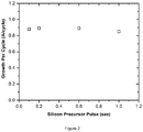
- Figure 2 shows the film thickness of as-deposited silicon nitride vs pulse time of Formula IIB precursor using nitrogen plasma at 300°C, demonstrating the self-limiting behavior even at 0.1 s and suggesting high reactivity of Formula IIB precursor.
- Figure 3 shows the film thickness of as-deposited silicon nitride vs the number of cycles using Formula IIB precursor and nitrogen plasma at 300°C, demonstrating the growth per cycle is about 0.9 ⁇ /cycle.
- steps b to e were repeated for 300 cycles except that the plasma power in step d was set to 250 Watts.
- the resultant film thickness of silicon nitride was 230 ⁇ , corresponding to a growth per cycle (GPC) of 0.77 ⁇ /cycle.
- the refractive index of the silicon nitride film was 2.0.
- the silicon wafer was loaded into the CN-1 reactor equipped with showerhead design with 13.56 MHz direct plasma and heated to 300°C with chamber pressure of 2 torr.
- Bis(disilylamino)silane was used as silicon precursor and ammonia plasma as plasma source.
- the ALD cycle was conducted using the following process parameters.
- Steps b to e were repeated for 300 cycles.
- the thickness of the as deposited silicon nitride was about 29 ⁇ , suggesting that the ammonia plasma is not as good of a nitrogen source compared to nitrogen plasma under similar conditions such as those in Example 2.
- the silicon wafer was loaded into the CN-1 reactor equipped with showerhead design with 13.56 MHz direct plasma and heated to 350°C with chamber pressure of 2 torr.
- Bis(disilylamino)silane was used as the silicon precursor.
- the ALD cycle was conducted using the following process parameters.
- Steps b to e were repeated for 200 cycles. No deposition was observed on the substrate when a plasma was not used compared to Example 3.
- the silicon wafer was loaded into the CN-1 reactor equipped with showerhead design with 13.56 MHz direct plasma and heated to 300°C with chamber pressure of 2 torr.
- Bis(disilylamino)silane was used as silicon precursor and nitrogen plasma as plasma source.
- the ALD cycle was conducted using the following process parameters.
- Steps b to e were repeated for 300 cycles.
- the thickness of as deposited silicon nitride was about 45 ⁇ , corresponding a GPC of 0.15 ⁇ /cycle. This experiment suggests hydrogen/nitrogen plasma is not a good nitrogen source compared to nitrogen plasma under the similar conditions such as Example 2.
- the silicon wafer was loaded into the CN-1 reactor equipped with showerhead design with 13.56 MHz direct plasma and heated to 300°C with chamber pressure of 2 torr.
- Bis(disilylamino)silane was employed as silicon precursor and nitrogen plasma as plasma source.
- the ALD cycle was conducted using the following process parameters.
- Steps b to e were repeated for 300 cycles.
- the thickness of as deposited silicon nitride was about 57 ⁇ , corresponding a GPC of 0.19 ⁇ /cycle.
- This experiment suggests changing the ratio of hydrogen vs nitrogen can improve the deposition rate of silicon nitride, however growth per cycle is still much lower than nitrogen plasma shown in Example 2.
- Another experiment was conducted using 1 sec pulse for the silicon precursor in step b, the thickness of as deposited silicon nitride was about 72 ⁇ , corresponding a GPC of 0.24 ⁇ /cycle.
Landscapes
- Chemical & Material Sciences (AREA)
- Engineering & Computer Science (AREA)
- Chemical Kinetics & Catalysis (AREA)
- General Chemical & Material Sciences (AREA)
- Organic Chemistry (AREA)
- Materials Engineering (AREA)
- Mechanical Engineering (AREA)
- Metallurgy (AREA)
- Inorganic Chemistry (AREA)
- Physics & Mathematics (AREA)
- Plasma & Fusion (AREA)
- Toxicology (AREA)
- Health & Medical Sciences (AREA)
- Electromagnetism (AREA)
- Formation Of Insulating Films (AREA)
- Chemical Vapour Deposition (AREA)
- Spectroscopy & Molecular Physics (AREA)
- Electrodes Of Semiconductors (AREA)
- Silicon Polymers (AREA)
Abstract
Description
- This Application claims the benefit of Application No.
62/068,248, filed on October 24, 2014 62/068,248 - Described herein is a process and a composition for the fabrication of an electronic device. More specifically, described herein are compositions for forming a silicon-containing film in a plasma enhanced atomic layer deposition (PEALD) process. Exemplary silicon-containing films that can be deposited using the compositions and methods described herein include, without limitation, stoichiometric or non-stoichiometric, silicon nitride, silicon carbonitride, silicon oxynitride, silicon aluminum nitride, silicon oxide, and silicon carboxide films.
- Silicon nitride is often used as an insulator and chemical barrier in manufacturing integrated circuits, to electrically isolate different structures or as an etch mask in bulk micromachining. As a passivation layer for microchips, it is superior to silicon dioxide, as it is a significantly better diffusion barrier against water molecules and sodium ions, two major sources of corrosion and instability in microelectronics. It is also used as a dielectric between polysilicon layers in capacitors in analog chips.
- One of the commercial methods for forming silicon nitride or films employs dichlorosilane and ammonia as the precursor reactants. Low pressure chemical vapor deposition (LPCVD) using precursors such as dichlorosilane and ammonia require high deposition temperatures to get the best film properties. For example, temperatures greater than 750°C may be required to obtain reasonable growth rates and uniformities. Other processing issues involve the hazardous aspects of chlorine and chlorine byproducts.
- Many of the newer semiconductor devices require silicon nitride films that have low etch rates, high film stresses, or both. It is also preferred, and sometimes necessary, that the films be formed at temperatures below 600°C while maintaining good electrical characteristics. Film hardness is yet another factor to consider in the design of the electrical components and the silicon nitride films do offer extremely hard films.
- The deposition of conformal, stoichiometric and non-stoichiometric silicon nitride films at low temperature, e.g., temperatures of about 500°C or less or about 400°C or less, which meet one or more criteria to be considered a high quality film, has been a long-standing industry challenge. There are several applications in semiconductor field such as advanced patterning or spacer which require high quality films. A silicon nitride film is considered a "high quality" film if it has one or more of the following characteristics: a density of 2.0 grams per cubic centimeter (g/cc) or greater, a low wet etch rate (as measured in dilute hydrofluoric acid (HF)), and combinations thereof compared to other silicon nitride films. In these or other embodiments, the refractive index for the silicon nitride film should be 1.8 or greater.
- Accordingly, there is a need in the art to provide a low temperature (e.g., processing temperature of about 500°C or less) method for depositing a conformal, high quality, silicon nitride film wherein the film has one or more of the following characteristics: a reflective index of 1.8 or higher, a density of 2.0 grams per cubic centimeter (g/cc) or greater, a low wet etch rate (as measured in dilute hydrofluoric acid (HF)), and combinations thereof compared to other silicon nitride films using other deposition methods or precursors.
- Described herein are methods and compositions for forming stoichiometric or non-stoichiometric silicon nitride films, which may further comprise carbon, oxygen, or combinations thereof, onto at least a portion of a substrate. In one aspect, the composition for depositing a silicon nitride film comprises: at least one silicon precursor compound selected from the group consisting of:


- In another aspect, there is provided a composition for forming a silicon-containing material comprising: (a) at least one silicon precursor compound selected from the group consisting of:


- In another aspect, there is provided a method for depositing a silicon nitride film, the method comprising:
- a. placing one or more substrates into a reactor;
- b. introducing at least one silicon precursor compound selected from the group consisting of:


- c. purging the reactor with a purge gas;
- d. introducing a plasma source comprising nitrogen into the reactor to react with at least a portion of the chemisorbed layer wherein the plasma is generated at a power density ranging from about 0.01 to about 1.5 W/cm2; and
- e. optionally purge the reactor with an inert gas; and wherein the steps b through e are repeated until a desired thickness of the silicon nitride film is obtained.
-
-
Figure 1 provides the relationship between silicon nitride film thickness measured in Angstroms (Å) and temperature of the plasma enhanced atomic layer deposition of silicon nitride using the Formula IIB precursor compound and method described in Example 2. -
Figure 2 provides the relationship between the growth of deposited film thickness measured in Å/cycle and silicon precursor pulse time (measured in seconds) for the precursor compound and method described in Example 2. -
Figure 3 provides the silicon nitride film thickness measured in Å versus the number of cycles using Formula IIB precursor and nitrogen plasma at 300°C described in Example 2. - The deposition of conformal, stoichiometric and non-stoichiometric silicon nitride films at low temperatures, e.g., temperatures of 500°C or less or 400°C or less, which meet one or more criteria to be considered a high quality film, has been a long-standing industry challenge. Throughout the description, the term "silicon nitride " as used herein refers to a film comprising silicon and nitrogen selected from the group consisting of stoichiometric or non-stoichiometric silicon nitride, silicon carbonitride, silicon carboxynitride, silicon aluminum nitride and there mixture thereof. A silicon nitride film is considered a "high quality" film if it has one or more of the following characteristics: a density of 2.0 grams per cubic centimeter (g/cc) or greater, a low wet etch rate (as measured in dilute hydrofluoric acid (HF)), and combinations thereof compared to other silicon nitride films. In these or other embodiments, the refractive index for the silicon nitride film should be 1.8 or higher. In one embodiment, described herein is composition for forming a silicon-containing film or material using silicon precursor compounds having Formulae IIA through IID. Also described herein is an atomic layer deposition (ALD) or ALD-like method that deposits a silicon nitride film at a low temperature, or one or more deposition temperatures ranging from about 20°C to about 500°C, using the Formula IIA through IID described herein in a plasma process which comprises nitrogen and optionally a noble or inert gas.
- Described herein are methods for forming a stoichiometric or non-stoichiometric silicon nitride film comprising silicon and nitrogen onto at least a portion of a substrate.
- In certain embodiments, the silicon nitride film may further comprise carbon. In certain embodiments, the silicon nitride film may further comprise aluminum such as a silicon aluminum nitride film. In certain embodiments, the silicon nitride film further comprises oxygen such as a silicon oxynitride film. In this or other embodiments, the silicon nitride film comprises oxygen and carbon such as a silicon carboxynitride film.
- In alternative embodiments, the composition comprising at least one silicon precursor compound having Formulae IIA through IID may be used to deposit a silicon oxide material or film. Throughout the description, the term "silicon oxide" as used herein refers to a film comprising silicon and nitrogen selected from the group consisting of stoichiometric or non-stoichiometric silicon oxide, carbon doped silicon oxide, silicon carboxynitride and mixtures thereof.
- The silicon nitride films described herein are deposited using at least one silicon precursor compound represented by Formulae IIA through IID below:


- While not being bound by theory, it is believed that the silicon precursor compounds having three or more Si-N bonds, and optionally three or more Si-H3 groups in Formula IIA, IIB and IID, are more reactive towards at least a portion of the substrate surface, thus anchoring more silicon fragments on the surface during the deposition process. This in turn will increase the growth rate of the film as well as provide better surface coverage for substrate comprising surface features, such as without limitation, pores, trenches, and/or vias, thereby allowing for the deposition of a conformal silicon nitride or other silicon-containing film on the surface. An example of a Formula IIB compound is bis(disilylamino)silane (aka N,N'-disilyltrisilazane). An example of a Formula IIC compound is tris (ethylsillyl) amine. In embodiments wherein the silicon precursor compound is tris(ethylsillyl)amine, it is believed that the ethylene acts as leaving group in the deposition process thereby creating additional Si reactive sites while at the same time lowering the Si-H content in the precursor.
- In Formulae IIA through IID above and throughout the description, the term "linear alkyl" denotes a linear functional group having from 1 to 10, 3 to 10, or 1 to 6 carbon atoms. Exemplary linear alkyl groups include, but are not limited to, methyl, ethyl, propyl, butyl, pentyl, and hexyl groups. In the formula IIA through IID above and throughout the description, the term "branched alkyl" denotes a branched functional group having from 3 to 10, or 1 to 6 carbon atoms. Exemplary branched alkyl groups include, but are not limited to, isopropyl, isobutyl, sec-butyl, tert-butyl, iso-pentyl, tert-pentyl, isohexyl, and neohexyl. In certain embodiments, the alkyl group may have one or more functional groups such as, but not limited to, an alkoxy group, a dialkylamino group or combinations thereof, attached thereto. In other embodiments, the alkyl group does not have one or more functional groups attached thereto. The alkyl group may be saturated or, alternatively, unsaturated.
- In Formulae IIA through IID above and throughout the description, the term "halide" denotes a chloride, bromide, iodide, or fluoride ion.
- In Formulae IIA through IID above and throughout the description, the term "cyclic alkyl" denotes a cyclic group having from 3 to 10 or 5 to 10 atoms. Exemplary cyclic alkyl groups include, but are not limited to, cyclobutyl, cyclopentyl, cyclohexyl, and cyclooctyl groups. In certain embodiments, the cyclic alkyl group may have one or more C1 to C10 linear, branched substituents, or substituents containing oxygen or nitrogen atoms. In this or other embodiments, the cyclic alkyl group may have one or more linear or branched alkyls or alkoxy groups as substituents, such as, for example, a methylcyclohexyl group or a methoxycyclohexyl group.
- In Formulae IIA through IID above and throughout the description, the term "aryl" denotes an aromatic cyclic functional group having from 3 to 10 carbon atoms, from 5 to 10 carbon atoms, or from 6 to 10 carbon atoms. Exemplary aryl groups include, but are not limited to, phenyl, benzyl, chlorobenzyl, tolyl, and o-xylyl.
- In Formulae IIA through IID above and throughout the description, the term "alkenyl group" denotes a group which has one or more carbon-carbon double bonds and has from 2 to 12, from 2 to 10, or from 2 to 6 carbon atoms. Exemplary alkenyl groups include, but are not limited to, vinyl or allyl groups.
- In Formulae IIA through IID above and throughout the description, the term "alkynyl group" denotes a group which has one or more carbon-carbon triple bonds and has from 2 to 12 or from 2 to 6 carbon atoms.
- In Formulae IIA through IID above and throughout the description, the term "unsaturated" as used herein means that the functional group, substituent, ring or bridge has one or more carbon double or triple bonds. An example of an unsaturated ring can be, without limitation, an aromatic ring such as a phenyl ring. The term "saturated" means that the functional group, substituent, ring or bridge does not have one or more double or triple bonds.
- In certain embodiments, one or more of the alkyl group, alkenyl group, alkynyl group, alkoxysilylalkyl group, alkoxy group, aryloxy, aroyloxy, aryl group, and/or aromatic group in the formulae may be "substituted" or have one or more atoms or group of atoms substituted in place of, for example, a hydrogen atom. Exemplary substituents include, but are not limited to, oxygen, sulfur, halogen atoms (e.g., F, CI, I, or Br), nitrogen, alkyl groups, and phosphorous. In other embodiments, one or more of the alkyl group, alkenyl group, alkynyl group, alkoxyalkyl group, alkoxy group, alkylaminoalkyl group, aromatic and/or aryl group in the formulae may be unsubstituted.
- The method used to form the silicon-containing materials and films described herein are deposition processes. Examples of suitable deposition processes for the method disclosed herein include, but are not limited to, plasma enhanced ALD (PEALD) or plasma enhanced cyclic CVD (PECCVD) process. As used herein, the term "chemical vapor deposition processes" refers to any process wherein a substrate is exposed to one or more volatile precursors, which react and/or decompose on the substrate surface to produce the desired deposition. As used herein, the term "atomic layer deposition process" refers to a self-limiting (e.g., the amount of film material deposited in each reaction cycle is constant), sequential surface chemistry that deposits silicon containing films of materials onto substrates of varying compositions. Although the precursors, reagents and sources used herein may be sometimes described as "gaseous", it is understood that the precursors can be either liquid or solid which are transported with or without an inert gas into the reactor via direct vaporization, bubbling or sublimation. In some case, the vaporized precursors can pass through a plasma generator. In one embodiment, the silicon nitride film is deposited using a plasma enhanced ALD process. In another embodiment, the silicon nitride film is deposited using a plasma enhanced CCVD process. The term "reactor" as used herein, includes without limitation, reaction chamber or deposition chamber. The ALD-like process is defined herein as a cyclic CVD process that provides a high conformal silicon nitride film such as, silicon nitride or silicon carbonitride on a substrate as shown by having at least one of the following: percentage of non-uniformity of about 5% or less as measured by ellipsometer, a deposition rate of 1 Å or greater per cycle, or a combination thereof.
- The silicon precursor compounds having Formulae IIA through IID may be delivered to the reaction chamber such as a CVD or ALD reactor in a variety of ways. In one embodiment, a liquid delivery system may be utilized. In an alternative embodiment, a combined liquid delivery and flash vaporization process unit may be employed, such as, for example, the turbo vaporizer manufactured by MSP Corporation of Shoreview, MN, to enable low volatility materials to be volumetrically delivered, which leads to reproducible transport and deposition without thermal decomposition of the precursor. In liquid delivery formulations, the precursors described herein may be delivered in neat liquid form, or alternatively, may be employed in solvent formulations or compositions comprising same. Thus, in certain embodiments the precursor formulations may include solvent component(s) of suitable character as may be desirable and advantageous in a given end use application to form a film on a substrate.
- In one embodiment of the method described herein, a substrate having a surface to which at least a portion of silicon-containing film or materials is deposited thereupon, is placed into a reactor deposition chamber. The temperature of the substrate may be controlled to be less than the walls of the reactor. The substrate temperature is held at a temperature from about room temperature (e.g., 20°C) to about 500°C. Alternative ranges for the substrate temperature have one or more of the following end points: 20, 50, 75, 100, 125, 150, 175, 200, 225, 250, 275, 300, 325, 350, 375, 400, 425, 450, 475, and 500°C. Exemplary temperature ranges include the following: 20 to 475°C, 100 to 400°C or 175 to 350°C.
- Depending upon the deposition method, in certain embodiments, the one or more silicon-containing precursor compounds may be introduced into the reactor at a predetermined molar volume, or from about 0.1 to about 1000 micromoles. In this or other embodiments, the silicon precursor or the silicon precursor comprising Formula IIA to IID and a solvent may be introduced into the reactor for a predetermined time period. In certain embodiments, the time period ranges from about 0.001 to about 500 seconds.
- In certain embodiments, the silicon-containing films comprise silicon nitride. In these embodiments, the silicon-containing films deposited using the methods described herein are formed in the presence of nitrogen-containing source. A nitrogen-containing source may be introduced into the reactor in the form of at least one nitrogen-containing source and/or may be present incidentally in the other precursors used in the deposition process. Suitable nitrogen-containing source gases may include, for example, ammonia, hydrazine, monoalkylhydrazine, dialkylhydrazine, plasma comprising nitrogen, plasma comprising nitrogen and hydrogen, plasma comprising nitrogen and helium, plasma comprising nitrogen and argon, ammonia plasma, plasma comprising nitrogen and ammonia, plasma comprising ammonia and helium, plasma comprising ammonia and argon plasma, NF3 plasma, organoamine plasma, and mixtures thereof. In other embodiments, the plasma is selected from the group consisting of hydrogen plasma, helium plasma, neon plasma, argon plasma, xenon plasma, hydrogen/helium plasma, hydrogen/argon plasma and mixtures thereof. In one particle embodiment, the nitrogen containing source is substantially free of (e.g., has 2 weight percent (wt. %) or less) hydrogen to avoid introducing additional hydrogen into the final silicon nitride film and is selected from the group consisting of nitrogen plasma, nitrogen/helium, nitrogen/argon plasma. In another embodiment, the nitrogen containing source is selected from monoalkylhydrazine, dialkylhydrazine. For deposition of silicon carbonitride, the nitrogen containing source can be selected from the group consisting of organic amine plasma such as methylamine plasma, dimethylamine plasma, trimethylamine plasma, ethylamine plasma, diethylamine plasma, trimethylamine plasma, ethylenediamine plasma. Throughout the description, the term "organic amine" as used herein describes organic compound has at least one nitrogen atom. Examples of organic amine, but are not limited to, methylamine, ethylamine, propylamine, iso-propylamine, tert-butylamine, sec-butylamine, tert-amylamine, ethylenediamine, dimethylamine, trimethylamine, diethylamine, pyrrole, 2,6-dimethylpiperidine, di-n-propylamine, di-iso-propylamine, ethylmethylamine, N-methylaniline, pyridine, triethylamine. Similarly, throughout the description, the term "organoamino group" as used herein refers to an organic group consisting of at least one nitrogen atom derived from secondary or primary organoamines as described above. "Organoamino group" does not include -NH2 group.
- In certain embodiments, the nitrogen-containing source is introduced into the reactor at a flow rate ranging from about 1 to about 2000 square cubic centimeters (sccm) or from about 1 to about 1000 sccm. The nitrogen-containing source can be introduced for a time that ranges from about 0.1 to about 100 seconds. In embodiments wherein the film is deposited by an ALD or a cyclic CVD process, the precursor pulse can have a pulse duration that is greater than 0.01 seconds, and the nitrogen-containing source can have a pulse duration that is less than 0.01 seconds. In yet another embodiment, the purge duration between the pulses that can be as low as 0 seconds or is continuously pulsed without a purge in-between.
- In certain embodiments, the silicon-containing films deposited using the methods described herein are formed in the presence of oxygen using an oxygen-containing source, reagent or precursor comprising oxygen. An oxygen-containing source may be introduced into the reactor in the form of at least one oxygen-containing source. In this or other embodiments, the oxygen-containing source may be present incidentally in the other precursors used in the deposition process. Suitable oxygen-containing source gases may include, for example, water (H2O) (e.g., deionized water, purifier water, and/or distilled water), oxygen (O2), oxygen plasma, ozone (O3), NO, N2O, NO2, carbon monoxide (CO), carbon dioxide (CO2) and combinations thereof. In certain embodiments, the oxygen-containing source is introduced into the reactor at a flow rate ranging from about 1 to about 2000 square cubic centimeters (sccm) or from about 1 to about 1000 sccm. The oxygen-containing source can be introduced for a time that ranges from about 0.1 to about 100 seconds. In one particular embodiment, the oxygen-containing source comprises water having a temperature of 10°C or greater. In embodiments wherein the film is deposited by an ALD or a cyclic CVD process, the precursor pulse can have a pulse duration that is greater than 0.01 seconds, and the oxygen-containing source can have a pulse duration that is less than 0.01 seconds, while the water pulse duration can have a pulse duration that is less than 0.01 seconds. In yet another embodiment, the purge duration between the pulses that can be as low as 0 seconds or is continuously pulsed without a purge in-between. The oxygen-containing source or reagent is provided in a molecular amount less than a 1:1 ratio to the silicon precursor, so that at least some carbon is retained in the as deposited silicon-containing film.
- In certain embodiments, the temperature of the reactor in the introducing step is at one or more temperatures ranging from about room temperature (e.g., 20°C) to about 500°C. Alternative ranges for the substrate temperature have one or more of the following end points: 20, 50, 75, 100, 125, 150, 175, 200, 225, 250, 275, 300, 325, 350, 375, 400, 425, 450, 475, and 500°C. Exemplary temperature ranges include the following: 20 to 475°C, 100 to 400°C or 175 to 350°C.
- Energy is applied to the at least one of the precursor compound, nitrogen-containing source, oxygen-containing source, other reagents, or a combination thereof to induce reaction and to form the silicon-containing film or coating or a chemisorbed layer on at least a portion of the substrate. Such energy can be provided by, but not limited to, thermal, plasma, pulsed plasma, helicon plasma, high density plasma, inductively coupled plasma, X-ray, e-beam, photon, remote plasma methods, and combinations thereof. In certain embodiments, a secondary RF frequency source can be used to modify the plasma characteristics at the substrate surface. In embodiments wherein the deposition involves plasma, the plasma-generated process may comprise a direct plasma-generated process in which plasma is directly generated in the reactor, or alternatively a remote plasma-generated process in which plasma is generated outside of the reactor and supplied into the reactor. In certain embodiments of the method described herein, the plasma is generated at a power density ranging from about 0.01 to about 1.5 W/cm2.
- The deposition methods disclosed herein may involve one or more purge gases. The purge gas, which is used to purge away unconsumed reactants and/or reaction byproducts, is an inert gas that does not react with the precursors. Exemplary purge gases include, but are not limited to, argon (Ar), nitrogen (N2), helium (He), neon, hydrogen (H2), and mixtures thereof. In certain embodiments, a purge gas is supplied into the reactor at a flow rate ranging from about 10 to about 2000 sccm for about 0.1 to 1000 seconds, thereby purging the unreacted material and any byproduct that may remain in the reactor.
- The respective step of supplying the precursors, oxygen-containing source, the nitrogen-containing source, and/or other precursors, source gases, and/or reagents may be performed by changing the time for supplying them to change the stoichiometric composition of the resultant film or material. A flow of argon and/or other gas may be employed as a carrier gas to help deliver the vapor of the at least one precursor compound to the reaction chamber during the precursor pulsing. In certain embodiments, the reaction chamber process pressure is about 10 Torr or less, 5 Torr or less, 2 Torr or less, 1 torr or less.
- In one embodiment of the ALD or CCVD method described herein, a substrate is heated on a heater stage in a reaction chamber that is exposed to the precursor compound initially to allow the compound to chemically adsorb onto the surface of the substrate. A purge gas such as nitrogen, argon, or other inert gas purges away unabsorbed excess precursor compound from the process chamber. After sufficient purging, a nitrogen-containing source may be introduced into reaction chamber to react with the absorbed surface followed by another gas purge to remove reaction by-products from the chamber. The process cycle can be repeated to achieve the desired film thickness. In other embodiments, pumping under vacuum can be used to remove unabsorbed excess precursor compound from the process chamber, after sufficient evacuation under pumping, a nitrogen-containing source may be introduced into reaction chamber to react with the absorbed surface followed by another pumping down purge to remove reaction by-products from the chamber. In yet another embodiment, the precursor compound and the nitrogen-containing source can be co-flowed into reaction chamber to react on the substrate surface to deposit silicon nitride. In a certain embodiment of cyclic CVD, the purge step is not used.
- In this or other embodiments, it is understood that the steps of the methods described herein may be performed in a variety of orders, may be performed sequentially or concurrently (e.g., during at least a portion of another step), and any combination thereof. The respective step of supplying the precursors and the nitrogen-containing source gases may be performed by varying the duration of the time for supplying them to change the stoichiometric composition of the resulting silicon-containing film.
- In one aspect, there is provided a method of forming a silicon nitride film, the method comprising the steps of:
- a. providing a substrate in a reactor;
- b. introducing into the reactor an at least one silicon precursor compound selected from the group consisting of:


- c. purging the reactor with a purge gas;
- d. introducing a plasma comprising nitrogen into the reactor to react with at least a portion of the chemisorbed layer and provide at least one reactive site; and
- e. optionally purge the reactor with an inert gas; and wherein the steps b through e are repeated until a desired thickness of the silicon nitride film is obtained.
- The silicon precursors described herein and compositions comprising the silicon precursors having three or more Si-N bonds, and optionally three or more Si-H3 groups represented by Formulae IIA through IID, according to the present invention are preferably substantially free of halide ions such as chloride or metal ions such as Al. As used herein, the term "substantially free" as it relates to halide ions (or halides) such as, for example, chlorides and fluorides, bromides, iodides, Al3+ ions, Fe2+, Fe3+, Ni2+, Cr3+ means less than 5 ppm (by weight), preferably less than 3 ppm, and more preferably less than 1 ppm, and most preferably 0 ppm. Chlorides or metal ions are known to act as decomposition catalysts for silicon precursors. Significant levels of chloride in the final product can cause the silicon precursors to degrade. The gradual degradation of the silicon precursors may directly impact the film deposition process making it difficult for the semiconductor manufacturer to meet film specifications. In addition, the shelf-life or stability is negatively impacted by the higher degradation rate of the silicon precursors thereby making it difficult to guarantee a 1-2 year shelf-life. Moreover, silicon precursors are known to form flammable and/or pyrophoric gases upon decomposition such as hydrogen and silane. Therefore, the accelerated decomposition of the silicon precursors presents safety and performance concerns related to the formation of these flammable and/or pyrophoric gaseous byproducts.
- Compositions according to the present invention that are substantially free of halides can be achieved by (1) reducing or eliminating chloride sources during chemical synthesis, and/or (2) implementing an effective purification process to remove chloride from the crude product such that the final purified product is substantially free of chlorides. Chloride sources may be reduced during synthesis by using reagents that do not contain halides such as chlorodislanes, bromodisilanes, or iododislanes thereby avoiding the production of by-products that contain halide ions. In addition, the aforementioned reagents should be substantially free of chloride impurities such that the resulting crude product is substantially free of chloride impurities. In a similar manner, the synthesis should not use halide based solvents, catalysts, or solvents which contain unacceptably high levels of halide contamination. The crude product may also be treated by various purification methods to render the final product substantially free of halides such as chlorides. Such methods are well described in the prior art and, may include, but are not limited to purification processes such as distillation, or adsorption. Distillation is commonly used to separate impurities from the desire product by exploiting differences in boiling point. Adsorption may also be used to take advantage of the differential adsorptive properties of the components to effect separation such that the final product is substantially free of halide. Adsorbents such as, for example, commercially available MgO-Al2O3 blends can be used to remove halides such as chloride.
- For those embodiments relating to a composition comprising a solvent(s) and a silicon precursor having Formulae IIA through IID described herein, the solvent or mixture thereof selected does not react with the silicon precursors. The amount of solvent by weight percentage in the composition ranges from 0.5% by weight to 99.5% or from 10% by weight to 75%. In this or other embodiments, the solvent has a boiling point (b.p.) similar to the b.p. of the silicon precursor precursors of Formula II or the difference between the b.p. of the solvent and the b.p. of the silicon precursor precursors of Formula II is 40°C or less, 30°C or less, or 20°C or less, 10°C or less, or 5°C or less. Alternatively, the difference between the boiling points ranges from any one or more of the following end-points: 0, 10, 20, 30, or 40°C. Examples of suitable ranges of b.p. difference include without limitation, 0 to 40°C, 20° to 30°C, or 10° to 30°C. Examples of suitable solvents in the compositions include, but are not limited to, an ether (such as 1,4-dioxane, dibutyl ether), a tertiary amine (such as pyridine, 1-methylpiperidine, 1-ethylpiperidine, N,N'-Dimethylpiperazine, N,N,N',N'-Tetramethylethylenediamine), a nitrile (such as benzonitrile), an alkyl hydrocarbon (such as octane, nonane, dodecane, ethylcyclohexane), an aromatic hydrocarbon (such as toluene, mesitylene), a tertiary aminoether (such as bis(2-dimethylaminoethyl) ether), or mixtures thereof. Some nonlimiting exemplary compositions include, but not limited to, a composition comprising bis(disilylamino)silane (b.p. about 135°C) and octane (b.p. 125 to 126°C); a composition comprising bis(disilylamino)silane (b.p. about 135°C) and ethylcyclohexane (b.p. 130-132°C); a composition comprising bis(disilylamino)silane (b.p. about 135°C) and cyclooctane (b.p. 149°C); a composition comprising bis(disilylamino)silane (b.p. about 135°C), and toluene (b.p. 115°C).
- In another embodiment, a vessel for depositing a silicon-containing film comprising one or more silicon precursor compound having Formulae IIA through IID is described herein. In one particular embodiment, the vessel comprises at least one pressurizable vessel (preferably of stainless steel) fitted with the proper valves and fittings to allow the delivery of one or more precursors to the reactor for a CVD or an ALD process. In this or other embodiments, the silicon precursor compound is provided in a pressurizable vessel comprised of stainless steel and the purity of the silicon precursor is 98% by weight or greater or 99.5% or greater which is suitable for the majority of semiconductor applications. In certain embodiments, such vessels can also have means for mixing the precursors with one or more additional precursor if desired. In these or other embodiments, the contents of the vessel(s) can be premixed with an additional precursor. Alternatively, the silicon precursor compounds described herein and/or other precursor can be maintained in separate vessels or in a single vessel having separation means for maintaining the silicon precursor having Formulae IIA through IID and other precursor separate during storage.
- In certain embodiments, the method described herein further comprises one or more additional silicon-containing precursors other than the silicon precursors having the above Formulae IIA through IID. Examples of additional silicon-containing precursors include, but are not limited to, monoaminosilane (e.g., di-iso-propylaminosilane, di-sec-butylaminosilane, phenylmethylaminosilane; organo-silicon compounds such as trisilylamine (TSA); monoaminosilane (di-iso-propylaminosilane, di-sec-butylaminosilane, phenylmethylaminosilane); siloxanes (e.g., hexamethyl disiloxane (HMDSO) and dimethyl siloxane (DMSO)); organosilanes (e.g., methylsilane, dimethylsilane, diethylsilane, vinyl trimethylsilane, trimethylsilane, tetramethylsilane, ethylsilane, disilylmethane, 2,4-disilapentane, 1,4-disilabutane, 2,5-disilahexane, 2,2-disilylpropane, 1,3,5-trisilacyclohexane and fluorinated derivatives of these compounds); phenyl-containing organo-silicon compounds (e.g., dimethylphenylsilane and diphenylmethylsilane); oxygen-containing organo-silicon compounds ,e.g., dimethyldimethoxysilane; 1,3,5,7-tetramethylcyclotetrasiloxane; 1,1,3,3-tetramethyldisiloxane; 1,3,5,7-tetrasila-4-oxo-heptane; 2,4,6,8-tetrasila-3,7-dioxo-nonane; 2,2-dimethyl-2,4,6,8-tetrasila-3,7-dioxo-nonane; octamethylcyclotetrasiloxane; [1,3,5,7,9]-pentamethylcyclopentasiloxane; 1,3,5,7-tetrasila-2,6-dioxo-cyclooctane; hexamethylcyclotrisiloxane; 1,3-dimethyldisiloxane; 1,3,5,7,9-pentamethylcyclopentasiloxane; hexamethoxydisiloxane, and fluorinated derivatives of these compounds.
- In certain embodiments, the silicon precursors having Formulae IIA through IID described herein can also be used as a dopant for metal containing films, such as but not limited to, metal oxide films or metal nitride films. In these embodiments, the metal containing film is deposited using an ALD or CVD process such as those processes described herein using metal alkoxide, metal amide, or volatile organometallic precursors. Examples of suitable metal alkoxide precursors that may be used with the method disclosed herein include, but are not limited to, group 3 to 6 metal alkoxide, group 3 to 6 metal complexes having both alkoxy and alkyl substituted cyclopentadienyl ligands, group 3 to 6 metal complexes having both alkoxy and alkyl substituted pyrrolyl ligands, group 3 to 6 metal complexes having both alkoxy and diketonate ligands; group 3 to 6 metal complexes having both alkoxy and ketoester ligands; Examples of suitable metal amide precursors that may be used with the method disclosed herein include, but are not limited to, AlCl3, trimethylaluminum (TMA), triethylaluminum, methylaluminum chloride, tris(dimethylamino)aluminum (TDMAA), tris(dimethylamino)aluminum (TDMAA), and tris(diethylamino)aluminum (TDEAA), and other volatile aluminum precursors, tetrakis(dimethylamino)zirconium (TDMAZ), tetrakis(diethylamino)zirconium (TDEAZ), tetrakis(ethylmethylamino)zirconium (TEMAZ), tetrakis(dimethylamino)hafnium (TDMAH), tetrakis(diethylamino)hafnium (TDEAH), and tetrakis(ethylmethylamino)hafnium (TEMAH), tetrakis(dimethylamino)titanium (TDMAT), tetrakis(diethylamino)titanium (TDEAT), tetrakis(ethylmethylamino)titanium (TEMAT), tert-butylimino tri(diethylamino)tantalum (TBTDET), tert-butylimino tri(dimethylamino)tantalum (TBTDMT), tert-butylimino tri(ethylmethylamino)tantalum (TBTEMT), ethylimino tri(diethylamino)tantalum (EITDET), ethylimino tri(dimethylamino)tantalum (EITDMT), ethylimino tri(ethylmethylamino)tantalum (EITEMT), tert-amylimino tri(dimethylamino)tantalum (TAIMAT), tert-amylimino tri(diethylamino)tantalum, pentakis(dimethylamino)tantalum, tert-amylimino tri(ethylmethylamino)tantalum, bis(tert-butylimino)bis(dimethylamino)tungsten (BTBMW), bis(tert-butylimino)bis(diethylamino)tungsten, bis(tert-butylimino)bis(ethylmethylamino)tungsten, and combinations thereof. Examples of suitable organometallic precursors that may be used with the method disclosed herein include, but are not limited to, group 3 metal cyclopentadienyls or alkyl cyclopentadienyls. Exemplary Group 3 to 6 metal herein include, but not limited to, Y, La, Ce, Pr, Nd, Sm, Eu, Gd, Tb, Dy, Er, Yb, Lu, Ti, Hf, Zr, V, Nb, Ta, Cr, Mo, and W.
- As mentioned previously, the method described herein may be used to deposit a silicon nitride film on at least a portion of a substrate. Examples of suitable substrates include but are not limited to, silicon, SiO2, Si3N4, OSG, FSG, silicon carbide, hydrogenated silicon carbide, silicon nitride, hydrogenated silicon nitride, silicon carbonitride, hydrogenated silicon carbonitride, boronitride, antireflective coatings, photoresists, a flexible substrate such as IGZO, organic polymers, porous organic and inorganic materials, metals such as copper and aluminum, and diffusion barrier layers such as but not limited to TiN, Ti(C)N, TaN, Ta(C)N, Ta, W, or WN. The films are compatible with a variety of subsequent processing steps such as, for example, chemical mechanical planarization (CMP) and anisotropic etching processes.
- The deposited films have applications, which include, but are not limited to, computer chips, optical devices, magnetic information storages, coatings on a supporting material or substrate, microelectromechanical systems (MEMS), nanoelectromechanical systems, thin film transistor (TFT), light emitting diodes (LED), organic light emitting diodes (OLED), IGZO, and liquid crystal displays (LCD).
- In certain embodiments, the substrate has a surface feature. In one particular embodiment, the substrate optionally has features on it of a small size less than 100 µm in width preferably less than 1 µm in width and most preferably less than 0.5 µm in width. The aspect ratio (the depth to width ratio) of the features, if present, is greater than 1:1 and preferably greater than 4:1 and most preferably greater than 8:1.
- The substrate may be a single crystal silicon wafer, a wafer of silicon carbide, a wafer of aluminum oxide (sapphire), a sheet of glass, a metallic foil, an organic polymer film or may be a polymeric, glass, silicon or metallic 3-dimensional article. The substrate may be coated with a variety of materials well known in the art including films of silicon oxide, silicon nitride, amorphous carbon, silicon oxycarbide, silicon oxynitride, silicon carbide, gallium arsenide, gallium nitride and the like. These coatings may completely coat the substrate, may be in multiple layers of various materials and may be partially etched to expose underlying layers of material. The surface may also have on it a photoresist material that has been exposed with a pattern and developed to partially coat the substrate.
- The following examples illustrate the method for depositing silicon-containing materials or films described herein and are not intended to limit it in any way.
- In the following examples, unless stated otherwise, properties were obtained from sample films that were deposited onto medium resistivity (14-17 Ω-cm) single crystal silicon wafer substrates. All film depositions were performed using the CN-1 reactor which has a showerhead design and uses 13.56 MHz direct plasma or the cross flow type CN-1 reactor without plasma (for comparative examples). In typical process conditions, unless stated otherwise, the chamber pressure was fixed at a pressure ranging from about 1 to about 5 torr. Additional inert gas such as argon or nitrogen was used to maintain chamber pressure. Typical RF power used was 125W over electrode area of 150 mm wafer susceptor to provide a power density of 0.7 W/cm2.
- Under the protection of nitrogen, 2.5 grams of a solution of B(C6F5)3 in dodecane (0.2 weight (wt.%), 9.8 x10⁻⁶ moles (mol)) was added to a 1 liter (L) round bottomed flask containing trisilylamine (500 g, 4.66 moles (mol)). Silane gas immediately began to evolve as gas bubbles. The reaction solution was stirred for approximately 1 hour while maintaining an internal temperature of 20°C. Once the mass of the reaction solution had decreased by 30%, 4,4-bipyridine was added (1.25 g, 8.00 x10⁻³ moles) as a catalyst poison, and the bubbling quickly stopped. After stirring the quenched reaction mixture for 2 h, the volatiles were vacuum transferred (25-35 °C/1 Torr) into a second 1 L flask chilled to -78 °C. The collected crude liquid was determined by gas chromatography (GC) and gas chromatography-mass spectroscopy (GC-MS) to be a ∼ 1:1 mixture of trisilylamine and N,N'-disilyltrisilazane. Purification by fractional vacuum-distillation (58 °C/50 Torr) yielded 164 g of N,N'-disilyltrisilazane as a colorless liquid with a purity of >99%. boiling point (b.p.) = 135 °C. GC-MS showed the following mass peaks: 181 (M-1), 149, 119, 104, 91, 72.
- The silicon wafer was loaded into the CN-1 reactor equipped with showerhead design with 13.56 MHz direct plasma and heated to 300°C with chamber pressure of 2 torr. Bis(disilylamino)silane was used as silicon precursor and nitrogen plasma as plasma source. The ALD cycle was conducted using the following process parameters.
- a. Prepare the reactor and load wafer
- ✔ Chamber pressure: 2 torr
- b. Introduce a silicon precursor to the reactor
- ✔ Total flow of nitrogen: 1000 standard cubic centimeters (sccm)
- ✔ silicon precursor pulse: 1 second
- c. Purge
- ✔ Total flow of nitrogen: 1000 sccm
- ✔ Purge time: 10 seconds
- d. Introduce plasma
- ✔ Total flow of nitrogen: 1000 sccm
- ✔ Plasma power: 125W
- ✔ Plasma pulse: 10 second
- e. Purge
- ✔ Total flow of nitrogen: 1000 sccm
- ✔ Purge time: 10 seconds
- Steps b to e were repeated for 300 cycles. The refractive index of the resulting silicon nitride film was 2.0 whereas the growth per cycle (GPC) was about 0.90Å/cycle, demonstrating high quality silicon nitride can be achieved using the bis(disilylamino)silane precursor compound.
- Additional experiments were designed to further confirm the PEALD behavior of bis(disilylamino)silane as silicon precursor.
Figure 1 shows the temperature dependence of the plasma enhanced atomic layer deposition of silicon nitride using Formula IIB precursor and nitrogen plasma, indicating that ALD window for this precursor is at least up to ∼ 400 °C.Figure 2 shows the film thickness of as-deposited silicon nitride vs pulse time of Formula IIB precursor using nitrogen plasma at 300°C, demonstrating the self-limiting behavior even at 0.1 s and suggesting high reactivity of Formula IIB precursor.Figure 3 shows the film thickness of as-deposited silicon nitride vs the number of cycles using Formula IIB precursor and nitrogen plasma at 300°C, demonstrating the growth per cycle is about 0.9Å/cycle. - In a further experiment, steps b to e were repeated for 300 cycles except that the plasma power in step d was set to 250 Watts. The resultant film thickness of silicon nitride was 230Å, corresponding to a growth per cycle (GPC) of 0.77Å/cycle. The refractive index of the silicon nitride film was 2.0.
- The silicon wafer was loaded into the CN-1 reactor equipped with showerhead design with 13.56 MHz direct plasma and heated to 300°C with chamber pressure of 2 torr. Bis(disilylamino)silane was used as silicon precursor and ammonia plasma as plasma source. The ALD cycle was conducted using the following process parameters.
- a. Prepare the reactor and load wafer
- ✔ Chamber pressure: 2 torr
- b. Introduce a silicon precursor to the reactor
- ✔ Total flow of argon: 1000 sccm
- ✔ silicon precursor pulse: 0.2 second
- c. Purge
- ✔ Total flow of argon: 1000 sccm
- ✔ Purge time: 10 seconds
- d. Introduce plasma
- ✔ Total flow of argon: 1000 sccm
- ✔ Total flow of ammonia: 500 sccm
- ✔ Plasma power: 125W
- ✔ Plasma pulse: 10 second
- e. Purge
- ✔ Total flow of nitrogen: 1000 sccm
- ✔ Purge time: 10 seconds
- Steps b to e were repeated for 300 cycles. The thickness of the as deposited silicon nitride was about 29Å, suggesting that the ammonia plasma is not as good of a nitrogen source compared to nitrogen plasma under similar conditions such as those in Example 2.
- Comparable Example 3. Thermal ALD Silicon Nitride Film Using Bis(disilylamino)silane (aka N,N'-disilyltrisilazane, Formula IIB) and Ammonia
- The silicon wafer was loaded into the CN-1 reactor equipped with showerhead design with 13.56 MHz direct plasma and heated to 350°C with chamber pressure of 2 torr. Bis(disilylamino)silane was used as the silicon precursor. The ALD cycle was conducted using the following process parameters.
- a. Prepare the reactor and load wafer
- ✔ Chamber pressure: 2 torr
- b. Introduce a silicon precursor to the reactor
- ✔ Total flow of argon: 1000 sccm
- ✔ silicon precursor pulse: 0.2 second
- c. Purge
- ✔ Total flow of argon: 1000 sccm
- ✔ Purge time: 10 seconds
- d. Introduce ammonia
- ✔ Total flow of argon: 1000 sccm
- ✔ Total flow of ammonia: 500 sccm
- ✔ Pulse: 10 second
- e. Purge
- ✔ Total flow of argon: 1000 sccm
- ✔ Purge time: 10 seconds
- Steps b to e were repeated for 200 cycles. No deposition was observed on the substrate when a plasma was not used compared to Example 3.
- The silicon wafer was loaded into the CN-1 reactor equipped with showerhead design with 13.56 MHz direct plasma and heated to 300°C with chamber pressure of 2 torr. Bis(disilylamino)silane was used as silicon precursor and nitrogen plasma as plasma source. The ALD cycle was conducted using the following process parameters.
- a. Prepare the reactor and load wafer
- ✔ Chamber pressure: 2 torr
- b. Introduce a silicon precursor to the reactor
- ✔ Total flow of nitrogen: 1000 sccm
- ✔ silicon precursor pulse: 0.2 second
- c. Purge
- ✔ Total flow of nitrogen: 1000 sccm
- ✔ Purge time: 10 seconds
- d. Introduce plasma
- ✔ Total flow of nitrogen: 1000 sccm
- ✔ Total flow of hydrogen: 500 sccm
- ✔ Plasma power: 125W
- ✔ Plasma pulse: 10 second
- e. Purge
- ✔ Total flow of nitrogen: 1000 sccm
- ✔ Purge time: 10 seconds
- Steps b to e were repeated for 300 cycles. The thickness of as deposited silicon nitride was about 45Å, corresponding a GPC of 0.15 Å/cycle. This experiment suggests hydrogen/nitrogen plasma is not a good nitrogen source compared to nitrogen plasma under the similar conditions such as Example 2.
- The silicon wafer was loaded into the CN-1 reactor equipped with showerhead design with 13.56 MHz direct plasma and heated to 300°C with chamber pressure of 2 torr. Bis(disilylamino)silane was employed as silicon precursor and nitrogen plasma as plasma source. The ALD cycle was conducted using the following process parameters.
- a. Prepare the reactor and load wafer
- ✔ Chamber pressure: 2 torr
- b. Introduce a silicon precursor to the reactor
- ✔ Total flow of nitrogen: 500 sccm
- ✔ Total flow of hydrogen: 500 sccm
- ✔ silicon precursor pulse: 0.2 second
- c. Purge
- ✔ Total flow of nitrogen: 500 sccm
- ✔ Total flow of hydrogen: 500 sccm
- ✔ Purge time: 10 seconds
- d. Introduce plasma
- ✔ Total flow of nitrogen: 500 sccm
- ✔ Total flow of hydrogen: 500 sccm
- ✔ Plasma power: 125W
- ✔ Plasma pulse: 10 second
- e. Purge
- ✔ Total flow of nitrogen: 1000 sccm
- ✔ Purge time: 10 seconds
- Steps b to e were repeated for 300 cycles. The thickness of as deposited silicon nitride was about 57Å, corresponding a GPC of 0.19 Å/cycle. This experiment suggests changing the ratio of hydrogen vs nitrogen can improve the deposition rate of silicon nitride, however growth per cycle is still much lower than nitrogen plasma shown in Example 2. Another experiment was conducted using 1 sec pulse for the silicon precursor in step b, the thickness of as deposited silicon nitride was about 72Å, corresponding a GPC of 0.24 Å/cycle.
Claims (10)
- A composition for depositing a silicon nitride or silicon oxide film, the composition comprising:at least one silicon precursor compound having the following Formulae IIA through IIB:


- A composition for forming a silicon-containing material:(a) at least one silicon precursor compound having the following Formulae IIA through IID:

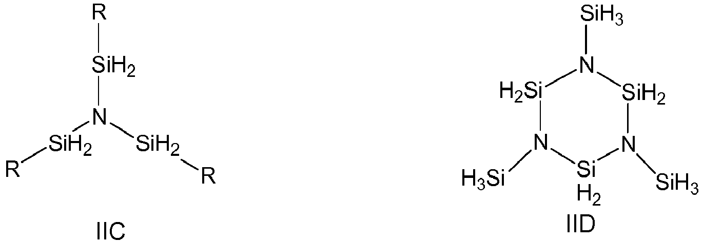 (b) a solvent wherein the solvent has a boiling point and the difference between the boiling point of the solvent and a boiling point of the silicon precursor is 40°C or less.
 - The composition of claim 2 wherein the compound comprises at least one selected from the group consisting of bis(disilylamino)silane and tri(ethylsilyl)amine.
- The composition of claim 3 wherein the compound comprises bis(disilylamino)silane.
- The composition of claim 2 comprising at least one selected from the group consisting of ether, tertiary amine, alkyl hydrocarbon, aromatic hydrocarbon, and tertiary aminoether.
- The composition of claim 2 wherein the solvent comprises at least one selected from the group consisting of octane, ethylcyclohexane, cyclooctane, and toluene.
- A method for depositing a silicon nitride film on at least a portion of a surface of a substrate, the method comprising:placing the substrate into a reactor;introducing into the reactor an at least one silicon precursor compound having the following Formulae IIA through IID:

 c. purging the reactor with a purge gas;d. introducing a plasma source comprising nitrogen into the reactor to react with at least a portion of the chemisorbed layer; ande. optionally purge the reactor with an inert gas; and wherein the steps b through e are repeated until a desired thickness of the silicon nitride film is obtained.
 - The method of claim 7 wherein the plasma source is selected from the group consisting of nitrogen plasma, nitrogen/helium plasma, nitrogen/argon plasma, ammonia plasma, ammonia/helium plasma, ammonia/argon/plasma, helium plasma, argon plasma, hydrogen plasma, hydrogen/helium plasma, hydrogen/argon plasma, organic amine plasma, and mixtures thereof.
- The method of claim 7 wherein the at least one silicon precursor compound comprises bis(disilylamino)silane.
- The method of claim 7 wherein the plasma in step d is generated at a power density ranging from about 0.01 to about 1.5 W/cm2.
Applications Claiming Priority (3)
| Application Number | Priority Date | Filing Date | Title |
|---|---|---|---|
| US201462068248P | 2014-10-24 | 2014-10-24 | |
| EP15790761.9A EP3209814B1 (en) | 2014-10-24 | 2015-10-23 | Compositions and methods using same for deposition of silicon-containing films |
| PCT/US2015/057045 WO2016065221A1 (en) | 2014-10-24 | 2015-10-23 | Compositions and methods using same for deposition of silicon-containing films |
Related Parent Applications (2)
| Application Number | Title | Priority Date | Filing Date |
|---|---|---|---|
| EP15790761.9A Division-Into EP3209814B1 (en) | 2014-10-24 | 2015-10-23 | Compositions and methods using same for deposition of silicon-containing films |
| EP15790761.9A Division EP3209814B1 (en) | 2014-10-24 | 2015-10-23 | Compositions and methods using same for deposition of silicon-containing films |
Publications (2)
| Publication Number | Publication Date |
|---|---|
| EP3431629A1 true EP3431629A1 (en) | 2019-01-23 |
| EP3431629B1 EP3431629B1 (en) | 2021-11-24 |
Family
ID=54477308
Family Applications (3)
| Application Number | Title | Priority Date | Filing Date |
|---|---|---|---|
| EP18180454.3A Active EP3431629B1 (en) | 2014-10-24 | 2015-10-23 | Compositions and methods using same for deposition of silicon-containing films |
| EP15790760.1A Active EP3209813B1 (en) | 2014-10-24 | 2015-10-23 | Compositions and methods using same for deposition of silicon-containing film |
| EP15790761.9A Active EP3209814B1 (en) | 2014-10-24 | 2015-10-23 | Compositions and methods using same for deposition of silicon-containing films |
Family Applications After (2)
| Application Number | Title | Priority Date | Filing Date |
|---|---|---|---|
| EP15790760.1A Active EP3209813B1 (en) | 2014-10-24 | 2015-10-23 | Compositions and methods using same for deposition of silicon-containing film |
| EP15790761.9A Active EP3209814B1 (en) | 2014-10-24 | 2015-10-23 | Compositions and methods using same for deposition of silicon-containing films |
Country Status (8)
| Country | Link |
|---|---|
| US (5) | US10316407B2 (en) |
| EP (3) | EP3431629B1 (en) |
| JP (4) | JP2017535077A (en) |
| KR (3) | KR102332415B1 (en) |
| CN (4) | CN113373428B (en) |
| SG (3) | SG11201703195QA (en) |
| TW (3) | TWI579399B (en) |
| WO (2) | WO2016065219A1 (en) |
Cited By (2)
| Publication number | Priority date | Publication date | Assignee | Title |
|---|---|---|---|---|
| EP3277698A4 (en) * | 2015-03-30 | 2019-03-20 | L'Air Liquide Société Anonyme pour l'Etude et l'Exploitation des Procédés Georges Claude | IS FILM-CONTAINING COMPOSITION AND METHODS OF USE |
| EP3307745A4 (en) * | 2015-06-12 | 2019-04-10 | L'Air Liquide Société Anonyme pour l'Etude et l'Exploitation des Procédés Georges Claude | VAPOR DEPOSITION PROCESSES FOR FORMING THIN FILMS CONTAINING SILICON AND NITROGEN |
Families Citing this family (90)
| Publication number | Priority date | Publication date | Assignee | Title |
|---|---|---|---|---|
| WO2015047914A1 (en) | 2013-09-27 | 2015-04-02 | Antonio Sanchez | Amine substituted trisilylamine and tridisilylamine compounds |
| US11549181B2 (en) * | 2013-11-22 | 2023-01-10 | Applied Materials, Inc. | Methods for atomic layer deposition of SiCO(N) using halogenated silylamides |
| SG11201703195QA (en) * | 2014-10-24 | 2017-05-30 | Versum Materials Us Llc | Compositions and methods using same for deposition of silicon-containing film |
| US10354860B2 (en) * | 2015-01-29 | 2019-07-16 | Versum Materials Us, Llc | Method and precursors for manufacturing 3D devices |
| US11124876B2 (en) | 2015-03-30 | 2021-09-21 | L'Air Liquide, Société Anonyme pour l'Etude et l'Exploitation des Procédés Georges Claude | Si-containing film forming precursors and methods of using the same |
| TWI706957B (en) * | 2015-03-30 | 2020-10-11 | 法商液態空氣喬治斯克勞帝方法研究開發股份有限公司 | Catalyst dehydrogenative coupling of carbosilanes with ammonia, amnines and amidines |
| EP3307744B1 (en) * | 2015-06-12 | 2020-09-02 | L'Air Liquide Société Anonyme pour l'Etude et l'Exploitation des Procédés Georges Claude | Vapor deposition processes for forming silicon- and oxygen-containing thin films |
| KR102692947B1 (en) * | 2015-10-22 | 2024-08-06 | 어플라이드 머티어리얼스, 인코포레이티드 | Methods for depositing flowable films comprising SiO and SiN |
| US9786491B2 (en) | 2015-11-12 | 2017-10-10 | Asm Ip Holding B.V. | Formation of SiOCN thin films |
| US12454753B2 (en) * | 2018-06-15 | 2025-10-28 | Versum Materials Us, Llc | Compositions and methods using same for deposition of silicon-containing film |
| KR102378021B1 (en) | 2016-05-06 | 2022-03-23 | 에이에스엠 아이피 홀딩 비.브이. | Formation of SiOC thin films |
| US20170372919A1 (en) * | 2016-06-25 | 2017-12-28 | Applied Materials, Inc. | Flowable Amorphous Silicon Films For Gapfill Applications |
| US9929006B2 (en) | 2016-07-20 | 2018-03-27 | Micron Technology, Inc. | Silicon chalcogenate precursors, methods of forming the silicon chalcogenate precursors, and related methods of forming silicon nitride and semiconductor structures |
| US20180033614A1 (en) * | 2016-07-27 | 2018-02-01 | Versum Materials Us, Llc | Compositions and Methods Using Same for Carbon Doped Silicon Containing Films |
| US11017998B2 (en) | 2016-08-30 | 2021-05-25 | Versum Materials Us, Llc | Precursors and flowable CVD methods for making low-K films to fill surface features |
| US10468244B2 (en) * | 2016-08-30 | 2019-11-05 | Versum Materials Us, Llc | Precursors and flowable CVD methods for making low-K films to fill surface features |
| US10811251B2 (en) | 2016-09-30 | 2020-10-20 | Intel Corporation | Dielectric gap-fill material deposition |
| US11735413B2 (en) * | 2016-11-01 | 2023-08-22 | Versum Materials Us, Llc | Precursors and flowable CVD methods for making low-k films to fill surface features |
| US10647578B2 (en) * | 2016-12-11 | 2020-05-12 | L'Air Liquide, Société Anonyme pour l'Etude et l'Exploitation des Procédés Georges Claude | N—H free and SI-rich per-hydridopolysilzane compositions, their synthesis, and applications |
| US10192734B2 (en) * | 2016-12-11 | 2019-01-29 | L'Air Liquide, Société Anonyme pour l'Etude et l'Exploration des Procédés Georges Claude | Short inorganic trisilylamine-based polysilazanes for thin film deposition |
| US11591692B2 (en) * | 2017-02-08 | 2023-02-28 | Versum Materials Us, Llc | Organoamino-polysiloxanes for deposition of silicon-containing films |
| US10822458B2 (en) * | 2017-02-08 | 2020-11-03 | Versum Materials Us, Llc | Organoamino-functionalized linear and cyclic oligosiloxanes for deposition of silicon-containing films |
| US10176984B2 (en) | 2017-02-14 | 2019-01-08 | Lam Research Corporation | Selective deposition of silicon oxide |
| US10242866B2 (en) | 2017-03-08 | 2019-03-26 | Lam Research Corporation | Selective deposition of silicon nitride on silicon oxide using catalytic control |
| US10224224B2 (en) | 2017-03-10 | 2019-03-05 | Micromaterials, LLC | High pressure wafer processing systems and related methods |
| KR102271768B1 (en) | 2017-04-07 | 2021-06-30 | 어플라이드 머티어리얼스, 인코포레이티드 | Gap Filling Using Reactive Annealing |
| US10559461B2 (en) | 2017-04-19 | 2020-02-11 | Lam Research Corporation | Selective deposition with atomic layer etch reset |
| JP7249952B2 (en) | 2017-05-05 | 2023-03-31 | エーエスエム アイピー ホールディング ビー.ブイ. | Plasma-enhanced deposition process for controlled formation of oxygen-containing thin films |
| US11177127B2 (en) * | 2017-05-24 | 2021-11-16 | Versum Materials Us, Llc | Functionalized cyclosilazanes as precursors for high growth rate silicon-containing films |
| US12057310B2 (en) | 2018-05-22 | 2024-08-06 | Versum Materials Us, Llc | Functionalized cyclosilazanes as precursors for high growth rate silicon-containing films |
| US10847360B2 (en) * | 2017-05-25 | 2020-11-24 | Applied Materials, Inc. | High pressure treatment of silicon nitride film |
| US10622214B2 (en) | 2017-05-25 | 2020-04-14 | Applied Materials, Inc. | Tungsten defluorination by high pressure treatment |
| CN110678973B (en) | 2017-06-02 | 2023-09-19 | 应用材料公司 | Dry stripping of boron carbide hard masks |
| TWI722292B (en) * | 2017-07-05 | 2021-03-21 | 美商應用材料股份有限公司 | Silicon nitride films with high nitrogen content |
| US10269571B2 (en) | 2017-07-12 | 2019-04-23 | Applied Materials, Inc. | Methods for fabricating nanowire for semiconductor applications |
| US10276411B2 (en) | 2017-08-18 | 2019-04-30 | Applied Materials, Inc. | High pressure and high temperature anneal chamber |
| KR102405723B1 (en) | 2017-08-18 | 2022-06-07 | 어플라이드 머티어리얼스, 인코포레이티드 | High pressure and high temperature annealing chamber |
| WO2019055415A1 (en) | 2017-09-12 | 2019-03-21 | Applied Materials, Inc. | Apparatus and methods for manufacturing semiconductor structures using protective barrier layer |
| TWI633201B (en) * | 2017-10-24 | 2018-08-21 | 國立交通大學 | Amorphous carbon thin film, manufacturing method thereof and optical system including the same |
| US10643867B2 (en) | 2017-11-03 | 2020-05-05 | Applied Materials, Inc. | Annealing system and method |
| EP3707746B1 (en) | 2017-11-11 | 2023-12-27 | Micromaterials LLC | Gas delivery system for high pressure processing chamber |
| WO2019099125A1 (en) | 2017-11-16 | 2019-05-23 | Applied Materials, Inc. | High pressure steam anneal processing apparatus |
| JP2021503714A (en) | 2017-11-17 | 2021-02-12 | アプライド マテリアルズ インコーポレイテッドApplied Materials,Incorporated | Capacitor system for high pressure processing system |
| US10460930B2 (en) | 2017-11-22 | 2019-10-29 | Lam Research Corporation | Selective growth of SiO2 on dielectric surfaces in the presence of copper |
| JP7299898B2 (en) | 2018-01-24 | 2023-06-28 | アプライド マテリアルズ インコーポレイテッド | Seam repair using high pressure annealing |
| TWI793262B (en) * | 2018-02-21 | 2023-02-21 | 法商液態空氣喬治斯克勞帝方法研究開發股份有限公司 | Perhydropolysilazane compositions and methods for forming nitride films using same |
| KR20200119852A (en) | 2018-02-21 | 2020-10-20 | 레르 리키드 쏘시에떼 아노님 뿌르 레뜌드 에렉스뿔라따시옹 데 프로세데 조르즈 클로드 | Perhydropolysilazane composition and method for forming oxide film using same |
| KR102539390B1 (en) * | 2018-02-22 | 2023-06-05 | 어플라이드 머티어리얼스, 인코포레이티드 | Methods for processing mask substrates to enable better film quality |
| US11404275B2 (en) | 2018-03-02 | 2022-08-02 | Lam Research Corporation | Selective deposition using hydrolysis |
| KR102702244B1 (en) | 2018-03-09 | 2024-09-03 | 어플라이드 머티어리얼스, 인코포레이티드 | High pressure annealing process for metal containing materials |
| SG11202008981TA (en) | 2018-03-28 | 2020-10-29 | Applied Materials Inc | Remote capacitively coupled plasma deposition of amorphous silicon |
| US10714331B2 (en) | 2018-04-04 | 2020-07-14 | Applied Materials, Inc. | Method to fabricate thermally stable low K-FinFET spacer |
| US10950429B2 (en) | 2018-05-08 | 2021-03-16 | Applied Materials, Inc. | Methods of forming amorphous carbon hard mask layers and hard mask layers formed therefrom |
| US10566188B2 (en) | 2018-05-17 | 2020-02-18 | Applied Materials, Inc. | Method to improve film stability |
| US10704141B2 (en) | 2018-06-01 | 2020-07-07 | Applied Materials, Inc. | In-situ CVD and ALD coating of chamber to control metal contamination |
| JP7113670B2 (en) * | 2018-06-08 | 2022-08-05 | 東京エレクトロン株式会社 | ALD film forming method and ALD film forming apparatus |
| SG11202011890XA (en) * | 2018-06-11 | 2020-12-30 | Versum Materials Us Llc | Compositions and methods using same for deposition of silicon-containing film |
| SG11202011887XA (en) * | 2018-06-15 | 2020-12-30 | Versum Materials Us Llc | Siloxane compositions and methods for using the compositions to deposit silicon containing films |
| US20200003937A1 (en) * | 2018-06-29 | 2020-01-02 | Applied Materials, Inc. | Using flowable cvd to gap fill micro/nano structures for optical components |
| JP6909762B2 (en) * | 2018-07-23 | 2021-07-28 | 株式会社Kokusai Electric | Semiconductor device manufacturing methods, board processing methods, board processing devices, and programs |
| US10748783B2 (en) | 2018-07-25 | 2020-08-18 | Applied Materials, Inc. | Gas delivery module |
| US10483099B1 (en) * | 2018-07-26 | 2019-11-19 | Asm Ip Holding B.V. | Method for forming thermally stable organosilicon polymer film |
| US10675581B2 (en) | 2018-08-06 | 2020-06-09 | Applied Materials, Inc. | Gas abatement apparatus |
| KR102409869B1 (en) | 2018-08-10 | 2022-06-16 | 버슘머트리얼즈 유에스, 엘엘씨 | Silicon compounds and methods for depositing films using same |
| EP3872223A3 (en) * | 2018-08-10 | 2021-11-17 | Versum Materials US, LLC | Silicon compounds and methods for depositing films using same |
| US10985010B2 (en) * | 2018-08-29 | 2021-04-20 | Versum Materials Us, Llc | Methods for making silicon and nitrogen containing films |
| JP7179172B6 (en) | 2018-10-30 | 2022-12-16 | アプライド マテリアルズ インコーポレイテッド | Method for etching structures for semiconductor applications |
| CN112996950B (en) | 2018-11-16 | 2024-04-05 | 应用材料公司 | Film deposition using enhanced diffusion process |
| WO2020117462A1 (en) | 2018-12-07 | 2020-06-11 | Applied Materials, Inc. | Semiconductor processing system |
| SG11202105970RA (en) * | 2018-12-21 | 2021-07-29 | Air Liquide | PRECURSORS AND PROCESSES FOR DEPOSITION OF SI-CONTAINING FILMS USING ALD AT TEMPERATURE OF 550ºC OR HIGHER |
| US11649547B2 (en) * | 2019-02-05 | 2023-05-16 | Versum Materials Us, Llc | Deposition of carbon doped silicon oxide |
| EP3942596A4 (en) * | 2019-03-20 | 2022-12-07 | Applied Materials, Inc. | THERMAL OXIDE GRADE LOW TEMPERATURE THICK OXIDE FILM GROWTH METHOD |
| KR102870167B1 (en) * | 2019-06-21 | 2025-10-14 | 버슘머트리얼즈 유에스, 엘엘씨 | Composition for deposition of silicon-containing film and method of use thereof |
| KR102829813B1 (en) * | 2019-10-08 | 2025-07-03 | 에스케이트리켐 주식회사 | Novel precursor for metal containing thin film, deposition method of film and semiconductor device of the same |
| KR102858491B1 (en) * | 2019-10-08 | 2025-09-10 | 에스케이트리켐 주식회사 | Precursor for group 5 metal containing thin film, deposition method of film and semiconductor device of the same |
| US11482414B2 (en) | 2019-12-18 | 2022-10-25 | L'Air Liquide, Société Anonyme pour l'Etude et l'Exploitation des Procédés Georges Claude | Ultra-low temperature ALD to form high-quality Si-containing film |
| TWI819257B (en) * | 2019-12-20 | 2023-10-21 | 美商應用材料股份有限公司 | Silicon carbonitride gapfill with tunable carbon content |
| KR102818620B1 (en) * | 2019-12-20 | 2025-06-10 | 삼성전자주식회사 | Method of forming material layer, integrated circuit device and method of manufacturing integrated circuit device |
| US11776846B2 (en) * | 2020-02-07 | 2023-10-03 | Asm Ip Holding B.V. | Methods for depositing gap filling fluids and related systems and devices |
| US11901222B2 (en) | 2020-02-17 | 2024-02-13 | Applied Materials, Inc. | Multi-step process for flowable gap-fill film |
| KR102855013B1 (en) * | 2020-05-27 | 2025-09-05 | 젤리스트 인코퍼레이티드 | Silicon-based thin films from N-alkyl substituted perhydridocyclotrisilazane |
| TWI797640B (en) | 2020-06-18 | 2023-04-01 | 法商液態空氣喬治斯克勞帝方法研究開發股份有限公司 | Silicon-based self-assembling monolayer compositions and surface preparation using the same |
| US11674222B2 (en) * | 2020-09-29 | 2023-06-13 | Applied Materials, Inc. | Method of in situ ceramic coating deposition |
| KR20250162947A (en) * | 2021-01-26 | 2025-11-19 | 엔테그리스, 아이엔씨. | High throughput deposition process |
| TW202248447A (en) * | 2021-03-08 | 2022-12-16 | 荷蘭商Asm Ip私人控股有限公司 | Methods and systems for forming a layer comprising aluminum, titanium, and carbon |
| CN117083412A (en) * | 2021-03-18 | 2023-11-17 | 弗萨姆材料美国有限责任公司 | Compositions for Atomic Layer Deposition of High Quality Silicon Oxide Thin Films |
| CN115565861A (en) * | 2021-07-02 | 2023-01-03 | 长鑫存储技术有限公司 | Thin film deposition method and semiconductor device |
| TW202315962A (en) * | 2021-09-08 | 2023-04-16 | 荷蘭商Asm Ip私人控股有限公司 | Topology-selective deposition method |
| EP4433625A4 (en) * | 2021-11-15 | 2025-10-01 | Versum Mat Us Llc | Multilayer silicon nitride film |
| CN118284718A (en) * | 2021-11-24 | 2024-07-02 | 恩特格里斯公司 | Organotin Precursor Compounds |
Citations (4)
| Publication number | Priority date | Publication date | Assignee | Title |
|---|---|---|---|---|
| US20090191722A1 (en) * | 2008-01-19 | 2009-07-30 | Tokyo Electron Limited | Film formation method and apparatus for semiconductor process |
| US20120213940A1 (en) * | 2010-10-04 | 2012-08-23 | Applied Materials, Inc. | Atomic layer deposition of silicon nitride using dual-source precursor and interleaved plasma |
| US20120220139A1 (en) * | 2009-10-14 | 2012-08-30 | Asm Japan K.K. | Method of depositing dielectric film by modified peald method |
| US20140256160A1 (en) * | 2011-11-21 | 2014-09-11 | Hitachi Kokusai Electric Inc. | Apparatus for Manufacturing Semiconductor Device, Method of Manufacturing Semiconductor Device, and Recording Medium |
Family Cites Families (124)
| Publication number | Priority date | Publication date | Assignee | Title |
|---|---|---|---|---|
| US4200666A (en) | 1978-08-02 | 1980-04-29 | Texas Instruments Incorporated | Single component monomer for silicon nitride deposition |
| JPS61234534A (en) * | 1985-04-11 | 1986-10-18 | Semiconductor Energy Lab Co Ltd | Fabrication of silicon nitride coating |
| US5008422A (en) | 1985-04-26 | 1991-04-16 | Sri International | Polysilazanes and related compositions, processes and uses |
| EP0218117A3 (en) | 1985-10-11 | 1989-11-23 | Allied Corporation | Cyclosilazane polymers as dielectric films in integrated circuit fabrication technology |
| JPH0662775B2 (en) | 1987-06-12 | 1994-08-17 | チッソ株式会社 | Novel polysilazane and method for producing the same |
| JP3060185B2 (en) | 1991-05-01 | 2000-07-10 | 株式会社高純度化学研究所 | Method for manufacturing silicon oxide film of semiconductor device |
| JPH06310493A (en) | 1993-04-23 | 1994-11-04 | Kawasaki Steel Corp | Manufacturing equipment for semiconductor device |
| JP3401322B2 (en) | 1993-08-26 | 2003-04-28 | 富士通株式会社 | Method for manufacturing semiconductor device having insulating film |
| US5567661A (en) | 1993-08-26 | 1996-10-22 | Fujitsu Limited | Formation of planarized insulating film by plasma-enhanced CVD of organic silicon compound |
| US5413813A (en) * | 1993-11-23 | 1995-05-09 | Enichem S.P.A. | CVD of silicon-based ceramic materials on internal surface of a reactor |
| US5424095A (en) * | 1994-03-07 | 1995-06-13 | Eniricerche S.P.A. | Ceramic vapor deposited coating using a steam-containing carrier gas and non-alkoxy silane precursors |
| JP3396791B2 (en) * | 1994-08-30 | 2003-04-14 | 富士通株式会社 | Method of forming insulating film |
| FR2759362B1 (en) * | 1997-02-10 | 1999-03-12 | Saint Gobain Vitrage | TRANSPARENT SUBSTRATE EQUIPPED WITH AT LEAST ONE THIN LAYER BASED ON SILICON NITRIDE OR OXYNITRIDE AND ITS PROCESS FOR OBTAINING IT |
| US5968611A (en) * | 1997-11-26 | 1999-10-19 | The Research Foundation Of State University Of New York | Silicon nitrogen-based films and method of making the same |
| US6197658B1 (en) | 1998-10-30 | 2001-03-06 | Taiwan Semiconductor Manufacturing Company | Sub-atmospheric pressure thermal chemical vapor deposition (SACVD) trench isolation method with attenuated surface sensitivity |
| US6541367B1 (en) * | 2000-01-18 | 2003-04-01 | Applied Materials, Inc. | Very low dielectric constant plasma-enhanced CVD films |
| US6630413B2 (en) * | 2000-04-28 | 2003-10-07 | Asm Japan K.K. | CVD syntheses of silicon nitride materials |
| JP4048112B2 (en) * | 2000-08-18 | 2008-02-13 | 東京エレクトロン株式会社 | Semiconductor device manufacturing method and semiconductor device |
| JP3915881B2 (en) * | 2001-03-14 | 2007-05-16 | 信越化学工業株式会社 | Method for producing branched low-molecular siloxane |
| JP2003203800A (en) * | 2001-09-14 | 2003-07-18 | Sekisui Chem Co Ltd | Atmospheric pressure plasma processing method and apparatus |
| US6969769B2 (en) * | 2002-06-14 | 2005-11-29 | Vanson Halosource, Inc. | N-halamine siloxanes for use in biocidal coatings and materials |
| JP4217870B2 (en) | 2002-07-15 | 2009-02-04 | 日本電気株式会社 | Organosiloxane copolymer film, manufacturing method thereof, growth apparatus, and semiconductor device using the copolymer film |
| WO2004016670A2 (en) * | 2002-08-16 | 2004-02-26 | The University Of Akron | Poly(cyclosiloxane) composiiton and method of synthesis thereof |
| WO2004113417A1 (en) * | 2003-05-23 | 2004-12-29 | Dow Corning Corporation | Siloxane resin-based anti-reflective coating composition having high wet etch rate |
| US7125582B2 (en) * | 2003-07-30 | 2006-10-24 | Intel Corporation | Low-temperature silicon nitride deposition |
| US20050109276A1 (en) * | 2003-11-25 | 2005-05-26 | Applied Materials, Inc. | Thermal chemical vapor deposition of silicon nitride using BTBAS bis(tertiary-butylamino silane) in a single wafer chamber |
| JP3666751B2 (en) | 2003-11-28 | 2005-06-29 | 東京エレクトロン株式会社 | Insulating film forming method and insulating film forming system |
| DE102004001288A1 (en) * | 2004-01-07 | 2005-08-11 | Clariant International Limited | Hydrophilic polysilazane-based coating |
| US7470450B2 (en) * | 2004-01-23 | 2008-12-30 | Intel Corporation | Forming a silicon nitride film |
| US7098150B2 (en) * | 2004-03-05 | 2006-08-29 | Air Liquide America L.P. | Method for novel deposition of high-k MSiON dielectric films |
| US7582555B1 (en) | 2005-12-29 | 2009-09-01 | Novellus Systems, Inc. | CVD flowable gap fill |
| US7524735B1 (en) | 2004-03-25 | 2009-04-28 | Novellus Systems, Inc | Flowable film dielectric gap fill process |
| US7074690B1 (en) | 2004-03-25 | 2006-07-11 | Novellus Systems, Inc. | Selective gap-fill process |
| US20050239295A1 (en) * | 2004-04-27 | 2005-10-27 | Wang Pei-L | Chemical treatment of material surfaces |
| US7521378B2 (en) | 2004-07-01 | 2009-04-21 | Micron Technology, Inc. | Low temperature process for polysilazane oxidation/densification |
| JP4470023B2 (en) * | 2004-08-20 | 2010-06-02 | レール・リキード−ソシエテ・アノニム・プール・レテュード・エ・レクスプロワタシオン・デ・プロセデ・ジョルジュ・クロード | Method for manufacturing silicon nitride film |
| US7332445B2 (en) * | 2004-09-28 | 2008-02-19 | Air Products And Chemicals, Inc. | Porous low dielectric constant compositions and methods for making and using same |
| KR101194125B1 (en) * | 2004-10-19 | 2012-10-25 | 도레이 카부시키가이샤 | Method for producing film, and, film |
| ATE486098T1 (en) * | 2004-12-17 | 2010-11-15 | Dow Corning | SILOXANE RESIN COATING |
| JP3788624B1 (en) * | 2005-01-18 | 2006-06-21 | 旭電化工業株式会社 | Composition comprising siloxane compound and phenol compound |
| JP2006261434A (en) | 2005-03-17 | 2006-09-28 | L'air Liquide Sa Pour L'etude & L'exploitation Des Procede S Georges Claude | Method for forming silicon oxide film |
| US7875556B2 (en) * | 2005-05-16 | 2011-01-25 | Air Products And Chemicals, Inc. | Precursors for CVD silicon carbo-nitride and silicon nitride films |
| JP4766934B2 (en) * | 2005-06-24 | 2011-09-07 | パナソニック株式会社 | Method for forming interlayer insulating film |
| CN101213322A (en) * | 2005-06-29 | 2008-07-02 | 乔治洛德方法研究和开发液化空气有限公司 | Deposition method of ternary film |
| JP2009500857A (en) | 2005-07-08 | 2009-01-08 | アヴィザ テクノロジー インコーポレイテッド | Method for depositing silicon-containing film |
| US20070010072A1 (en) * | 2005-07-09 | 2007-01-11 | Aviza Technology, Inc. | Uniform batch film deposition process and films so produced |
| JP4305427B2 (en) * | 2005-08-02 | 2009-07-29 | 東京エレクトロン株式会社 | Film forming method, film forming apparatus, and storage medium |
| US7547796B2 (en) * | 2005-09-29 | 2009-06-16 | Praxair Technology, Inc. | Organometallic compounds, processes for the preparation thereof and methods of use thereof |
| US8530361B2 (en) * | 2006-05-23 | 2013-09-10 | Air Products And Chemicals, Inc. | Process for producing silicon and oxide films from organoaminosilane precursors |
| US7875312B2 (en) * | 2006-05-23 | 2011-01-25 | Air Products And Chemicals, Inc. | Process for producing silicon oxide films for organoaminosilane precursors |
| US7498273B2 (en) | 2006-05-30 | 2009-03-03 | Applied Materials, Inc. | Formation of high quality dielectric films of silicon dioxide for STI: usage of different siloxane-based precursors for harp II—remote plasma enhanced deposition processes |
| US7781352B2 (en) | 2007-06-06 | 2010-08-24 | Asm Japan K.K. | Method for forming inorganic silazane-based dielectric film |
| KR101593352B1 (en) | 2007-06-28 | 2016-02-15 | 인티그리스, 인코포레이티드 | Precursors for silicon dioxide gap fill |
| JP2009032962A (en) | 2007-07-27 | 2009-02-12 | Panasonic Corp | Semiconductor device and manufacturing method thereof |
| US7999355B2 (en) * | 2008-07-11 | 2011-08-16 | Air Products And Chemicals, Inc. | Aminosilanes for shallow trench isolation films |
| US20100081293A1 (en) | 2008-10-01 | 2010-04-01 | Applied Materials, Inc. | Methods for forming silicon nitride based film or silicon carbon based film |
| JP5559988B2 (en) | 2009-06-03 | 2014-07-23 | 東京エレクトロン株式会社 | Film forming material for silicon oxide film and method for forming silicon oxide film using the same |
| US7825040B1 (en) | 2009-06-22 | 2010-11-02 | Asm Japan K.K. | Method for depositing flowable material using alkoxysilane or aminosilane precursor |
| JP5011355B2 (en) * | 2009-07-30 | 2012-08-29 | 東京エレクトロン株式会社 | Deposition method |
| SG178061A1 (en) | 2009-08-25 | 2012-03-29 | Semiconductor Energy Lab | Method for reprocessing semiconductor substrate, method for manufacturing reprocessed semiconductor substrate, and method for manufacturing soi substrate |
| TW201131651A (en) * | 2009-10-05 | 2011-09-16 | Univ Tohoku | Low dielectric constant insulating film |
| US20110136347A1 (en) * | 2009-10-21 | 2011-06-09 | Applied Materials, Inc. | Point-of-use silylamine generation |
| WO2011058947A1 (en) * | 2009-11-11 | 2011-05-19 | 日本電気株式会社 | Variable resistance element, semiconductor device, and method for forming variable resistance element |
| US20110151677A1 (en) * | 2009-12-21 | 2011-06-23 | Applied Materials, Inc. | Wet oxidation process performed on a dielectric material formed from a flowable cvd process |
| CN102754193A (en) | 2010-01-06 | 2012-10-24 | 应用材料公司 | Flowable dielectric using oxide liner |
| JP5623296B2 (en) * | 2010-01-15 | 2014-11-12 | 信越化学工業株式会社 | Method for producing trisilylamine |
| US8703625B2 (en) * | 2010-02-04 | 2014-04-22 | Air Products And Chemicals, Inc. | Methods to prepare silicon-containing films |
| EP2362411A1 (en) * | 2010-02-26 | 2011-08-31 | Nederlandse Organisatie voor toegepast -natuurwetenschappelijk onderzoek TNO | Apparatus and method for reactive ion etching |
| US20120083133A1 (en) | 2010-10-05 | 2012-04-05 | Applied Materials, Inc. | Amine curing silicon-nitride-hydride films |
| US8455768B2 (en) * | 2010-11-15 | 2013-06-04 | International Business Machines Corporation | Back-end-of-line planar resistor |
| US8685867B1 (en) | 2010-12-09 | 2014-04-01 | Novellus Systems, Inc. | Premetal dielectric integration process |
| US8460753B2 (en) | 2010-12-09 | 2013-06-11 | Air Products And Chemicals, Inc. | Methods for depositing silicon dioxide or silicon oxide films using aminovinylsilanes |
| US8530983B2 (en) * | 2011-04-08 | 2013-09-10 | Georgia Tech Research Corporation | Piezo-phototronic effect devices |
| US8592005B2 (en) * | 2011-04-26 | 2013-11-26 | Asm Japan K.K. | Atomic layer deposition for controlling vertical film growth |
| DE102011075974A1 (en) * | 2011-05-17 | 2012-11-22 | Evonik Degussa Gmbh | Process for the preparation of trisilylamine in the gas phase |
| US20130209343A1 (en) * | 2012-02-10 | 2013-08-15 | American Air Liquide, Inc. | Liquid phase synthesis of trisilylamine |
| US8846536B2 (en) | 2012-03-05 | 2014-09-30 | Novellus Systems, Inc. | Flowable oxide film with tunable wet etch rate |
| US8871656B2 (en) | 2012-03-05 | 2014-10-28 | Applied Materials, Inc. | Flowable films using alternative silicon precursors |
| CN104271797B (en) | 2012-03-09 | 2017-08-25 | 弗萨姆材料美国有限责任公司 | Barrier materials for display devices |
| JP5949027B2 (en) * | 2012-03-23 | 2016-07-06 | 富士ゼロックス株式会社 | Electrostatic image developing toner, electrostatic image developer, toner cartridge, developer cartridge, process cartridge, image forming apparatus, and image forming method |
| US20130260575A1 (en) | 2012-03-28 | 2013-10-03 | Air Products And Chemicals, Inc. | Silicon precursors and compositions comprising same for depositing low dielectric constant films |
| US9337018B2 (en) | 2012-06-01 | 2016-05-10 | Air Products And Chemicals, Inc. | Methods for depositing films with organoaminodisilane precursors |
| US9978585B2 (en) * | 2012-06-01 | 2018-05-22 | Versum Materials Us, Llc | Organoaminodisilane precursors and methods for depositing films comprising same |
| US10211310B2 (en) * | 2012-06-12 | 2019-02-19 | Novellus Systems, Inc. | Remote plasma based deposition of SiOC class of films |
| WO2014015248A1 (en) * | 2012-07-20 | 2014-01-23 | L'air Liquide, Societe Anonyme Pour L'etude Et L'exploitation Des Procedes Georges Claude | Organosilane precursors for ald/cvd silicon-containing film applications |
| US9243324B2 (en) | 2012-07-30 | 2016-01-26 | Air Products And Chemicals, Inc. | Methods of forming non-oxygen containing silicon-based films |
| DE102012214290A1 (en) * | 2012-08-10 | 2014-02-13 | Evonik Industries Ag | Process for the coupled preparation of polysilazanes and trisilylamine |
| KR101361454B1 (en) * | 2012-08-23 | 2014-02-21 | 이근수 | Method for forming silicone oxide film of semiconductor device |
| US8889566B2 (en) | 2012-09-11 | 2014-11-18 | Applied Materials, Inc. | Low cost flowable dielectric films |
| US9330899B2 (en) * | 2012-11-01 | 2016-05-03 | Asm Ip Holding B.V. | Method of depositing thin film |
| US9878234B2 (en) * | 2012-12-10 | 2018-01-30 | Arlen Moller | Incorporating objective assessments of fantasy-team-owners' physical activity into fantasy sport platforms |
| US10279959B2 (en) | 2012-12-11 | 2019-05-07 | Versum Materials Us, Llc | Alkoxysilylamine compounds and applications thereof |
| KR101599952B1 (en) * | 2012-12-31 | 2016-03-04 | 제일모직 주식회사 | Methods of producing polymers and compositions for forming silica insulation films |
| KR101583232B1 (en) | 2012-12-31 | 2016-01-07 | 제일모직 주식회사 | Methods of producing polymers and compositions for forming silica insulation films |
| US9343545B2 (en) | 2013-03-06 | 2016-05-17 | International Business Machines Corporation | Electrical coupling of memory cell access devices to a word line |
| DE102013209802A1 (en) * | 2013-05-27 | 2014-11-27 | Evonik Industries Ag | Process for the coupled preparation of trisilylamine and polysilazanes having a molecular weight of up to 500 g / mol |
| KR101600337B1 (en) * | 2013-06-07 | 2016-03-08 | (주)디엔에프 | Novel amino-silyl amine compound, method for manufacturing thereof and silicon-containing thin film use the same |
| WO2015047914A1 (en) * | 2013-09-27 | 2015-04-02 | Antonio Sanchez | Amine substituted trisilylamine and tridisilylamine compounds |
| US9905415B2 (en) * | 2013-10-03 | 2018-02-27 | Versum Materials Us, Llc | Methods for depositing silicon nitride films |
| WO2015112324A1 (en) * | 2014-01-24 | 2015-07-30 | Applied Materials, Inc. | Deposition of silicon and oxygen-containing films without an oxidizer |
| JP6345006B2 (en) * | 2014-07-08 | 2018-06-20 | キヤノン株式会社 | Manufacturing method of substrate for ink jet recording head |
| US20160079034A1 (en) * | 2014-09-12 | 2016-03-17 | Applied Materials Inc. | Flowable film properties tuning using implantation |
| US20160156066A1 (en) * | 2014-10-20 | 2016-06-02 | Massachusetts Institute Of Technology | Polymer electrolytes for electrochemical cells |
| SG11201703195QA (en) * | 2014-10-24 | 2017-05-30 | Versum Materials Us Llc | Compositions and methods using same for deposition of silicon-containing film |
| US10354860B2 (en) * | 2015-01-29 | 2019-07-16 | Versum Materials Us, Llc | Method and precursors for manufacturing 3D devices |
| US11001599B2 (en) * | 2015-03-23 | 2021-05-11 | Gelest Technologies, Inc. | N-alkyl substituted cyclic and oligomeric perhydridosilazanes, methods of preparation thereof, and silicon nitride films formed therefrom |
| US9777025B2 (en) | 2015-03-30 | 2017-10-03 | L'Air Liquide, Société pour l'Etude et l'Exploitation des Procédés Georges Claude | Si-containing film forming precursors and methods of using the same |
| US11124876B2 (en) * | 2015-03-30 | 2021-09-21 | L'Air Liquide, Société Anonyme pour l'Etude et l'Exploitation des Procédés Georges Claude | Si-containing film forming precursors and methods of using the same |
| KR20170019668A (en) * | 2015-08-12 | 2017-02-22 | (주)디엔에프 | The manufacturing method of the silicon nitride film by using plasma enhanced atomic layer deposition |
| KR102692947B1 (en) * | 2015-10-22 | 2024-08-06 | 어플라이드 머티어리얼스, 인코포레이티드 | Methods for depositing flowable films comprising SiO and SiN |
| TWI617693B (en) * | 2015-12-21 | 2018-03-11 | Versum Materials Us, Llc | Composition for depositing ruthenium containing film and method therefor |
| US12454753B2 (en) * | 2018-06-15 | 2025-10-28 | Versum Materials Us, Llc | Compositions and methods using same for deposition of silicon-containing film |
| CN114231947A (en) | 2016-02-26 | 2022-03-25 | 弗萨姆材料美国有限责任公司 | Compositions and methods of depositing silicon-containing films using the same |
| US10384944B2 (en) * | 2016-05-19 | 2019-08-20 | L'Air Liquide, Société Anonyme pour l'Etude et l'Exploitation des Procédés Georges Claude | Preparation of Si—H containing iodosilanes via halide exchange reaction |
| US20180033614A1 (en) * | 2016-07-27 | 2018-02-01 | Versum Materials Us, Llc | Compositions and Methods Using Same for Carbon Doped Silicon Containing Films |
| US11017998B2 (en) * | 2016-08-30 | 2021-05-25 | Versum Materials Us, Llc | Precursors and flowable CVD methods for making low-K films to fill surface features |
| US10468244B2 (en) * | 2016-08-30 | 2019-11-05 | Versum Materials Us, Llc | Precursors and flowable CVD methods for making low-K films to fill surface features |
| US11735413B2 (en) * | 2016-11-01 | 2023-08-22 | Versum Materials Us, Llc | Precursors and flowable CVD methods for making low-k films to fill surface features |
| US10647578B2 (en) * | 2016-12-11 | 2020-05-12 | L'Air Liquide, Société Anonyme pour l'Etude et l'Exploitation des Procédés Georges Claude | N—H free and SI-rich per-hydridopolysilzane compositions, their synthesis, and applications |
| CN111295465B (en) * | 2017-09-14 | 2022-12-09 | 弗萨姆材料美国有限责任公司 | Compositions and methods for depositing silicon-containing films |
| US11049714B2 (en) * | 2017-09-19 | 2021-06-29 | Versum Materials Us, Llc | Silyl substituted organoamines as precursors for high growth rate silicon-containing films |
| US11078569B2 (en) * | 2017-09-19 | 2021-08-03 | Versum Materials Us, Llc | Trisilylamine derivatives as precursors for high growth rate silicon-containing films |
| US20190318925A1 (en) * | 2018-04-11 | 2019-10-17 | Versum Materials Us, Llc | Monoorganoaminodisilane Precursors and Methods for Depositing Films Comprising Same |
| US12264258B2 (en) * | 2019-07-25 | 2025-04-01 | Versum Materials Us, Llc | Compositions comprising silacycloalkanes and methods using same for deposition of silicon-containing film |
-
2015
- 2015-10-23 SG SG11201703195QA patent/SG11201703195QA/en unknown
- 2015-10-23 CN CN202110661668.0A patent/CN113373428B/en active Active
- 2015-10-23 EP EP18180454.3A patent/EP3431629B1/en active Active
- 2015-10-23 SG SG10202000545RA patent/SG10202000545RA/en unknown
- 2015-10-23 JP JP2017522032A patent/JP2017535077A/en not_active Withdrawn
- 2015-10-23 KR KR1020207034642A patent/KR102332415B1/en active Active
- 2015-10-23 SG SG11201703196WA patent/SG11201703196WA/en unknown
- 2015-10-23 KR KR1020177013994A patent/KR102079501B1/en active Active
- 2015-10-23 US US15/520,330 patent/US10316407B2/en active Active
- 2015-10-23 EP EP15790760.1A patent/EP3209813B1/en active Active
- 2015-10-23 EP EP15790761.9A patent/EP3209814B1/en active Active
- 2015-10-23 WO PCT/US2015/057040 patent/WO2016065219A1/en not_active Ceased
- 2015-10-23 JP JP2017522023A patent/JP6871161B2/en active Active
- 2015-10-23 WO PCT/US2015/057045 patent/WO2016065221A1/en not_active Ceased
- 2015-10-23 CN CN201580067146.0A patent/CN107429391B/en active Active
- 2015-10-23 CN CN201580067222.8A patent/CN107257867B/en active Active
- 2015-10-23 CN CN202110244436.5A patent/CN113025992B/en active Active
- 2015-10-23 US US15/520,326 patent/US10106890B2/en active Active
- 2015-10-23 KR KR1020177013995A patent/KR102188751B1/en active Active
- 2015-10-26 TW TW104135153A patent/TWI579399B/en active
- 2015-10-26 TW TW106103536A patent/TWI658168B/en active
- 2015-10-26 TW TW104135152A patent/TWI575102B/en active
-
2018
- 2018-09-18 US US16/134,410 patent/US12049695B2/en active Active
-
2019
- 2019-04-18 US US16/388,225 patent/US20190271075A1/en active Pending
- 2019-09-09 JP JP2019164049A patent/JP6949912B2/en active Active
-
2021
- 2021-09-17 JP JP2021152399A patent/JP7152576B2/en active Active
-
2024
- 2024-07-29 US US18/787,871 patent/US20250188605A1/en active Pending
Patent Citations (4)
| Publication number | Priority date | Publication date | Assignee | Title |
|---|---|---|---|---|
| US20090191722A1 (en) * | 2008-01-19 | 2009-07-30 | Tokyo Electron Limited | Film formation method and apparatus for semiconductor process |
| US20120220139A1 (en) * | 2009-10-14 | 2012-08-30 | Asm Japan K.K. | Method of depositing dielectric film by modified peald method |
| US20120213940A1 (en) * | 2010-10-04 | 2012-08-23 | Applied Materials, Inc. | Atomic layer deposition of silicon nitride using dual-source precursor and interleaved plasma |
| US20140256160A1 (en) * | 2011-11-21 | 2014-09-11 | Hitachi Kokusai Electric Inc. | Apparatus for Manufacturing Semiconductor Device, Method of Manufacturing Semiconductor Device, and Recording Medium |
Non-Patent Citations (2)
| Title |
|---|
| RICHARD L. WELLS ET AL, JOURNAL OF THE AMERICAN CHEMICAL SOCIETY, vol. 88, no. 1, 5 January 1966 (1966-01-05), pages 37 - 42, XP055080155, ISSN: 0002-7863, DOI: 10.1021/ja00953a008 * |
| WILLIAM M. SCANTLIN ET AL: "Borane-catalyzed condensation of trisilazane and N-methyldisilazane", INORGANIC CHEMISTRY, vol. 11, no. 12, 1 December 1972 (1972-12-01), EASTON, US, pages 3082 - 3084, XP055245955, ISSN: 0020-1669, DOI: 10.1021/ic50118a041 * |
Cited By (2)
| Publication number | Priority date | Publication date | Assignee | Title |
|---|---|---|---|---|
| EP3277698A4 (en) * | 2015-03-30 | 2019-03-20 | L'Air Liquide Société Anonyme pour l'Etude et l'Exploitation des Procédés Georges Claude | IS FILM-CONTAINING COMPOSITION AND METHODS OF USE |
| EP3307745A4 (en) * | 2015-06-12 | 2019-04-10 | L'Air Liquide Société Anonyme pour l'Etude et l'Exploitation des Procédés Georges Claude | VAPOR DEPOSITION PROCESSES FOR FORMING THIN FILMS CONTAINING SILICON AND NITROGEN |
Also Published As
Similar Documents
| Publication | Publication Date | Title |
|---|---|---|
| EP3209814B1 (en) | Compositions and methods using same for deposition of silicon-containing films | |
| US20240093366A1 (en) | Compositions and methods for depositing silicon-containing films | |
| EP3329032B1 (en) | Compositions and methods for depositing silicon nitride films | |
| US20200365401A1 (en) | Boron-Containing Compounds, Compositions, And Methods For The Deposition Of A Boron Containing Films | |
| EP2392691B1 (en) | Organoaminosilane precursors and methods for depositing films comprising the same | |
| KR102866313B1 (en) | Composition for silicon-containing film and method of using same | |
| US20170183502A1 (en) | Organoaminodisilane Precursors and Methods for Depositing Films Comprising Same | |
| EP3516089A1 (en) | Compositions and methods for the deposition of silicon oxide films | |
| EP2669249A1 (en) | Organoaminodisilane precursors and methods for depositing films comprising same | |
| WO2020242868A1 (en) | Organosilicon precursors for deposition of silicon-containing films | |
| TW202138379A (en) | Organoamino-functionalized cyclic oligosiloxanes for deposition of silicon-containing films | |
| WO2022020705A1 (en) | Compositions and methods using same for germanium seed layer |
Legal Events
| Date | Code | Title | Description |
|---|---|---|---|
| PUAI | Public reference made under article 153(3) epc to a published international application that has entered the european phase |
Free format text: ORIGINAL CODE: 0009012 |
|
| STAA | Information on the status of an ep patent application or granted ep patent |
Free format text: STATUS: THE APPLICATION HAS BEEN PUBLISHED |
|
| AC | Divisional application: reference to earlier application |
Ref document number: 3209814 Country of ref document: EP Kind code of ref document: P |
|
| AK | Designated contracting states |
Kind code of ref document: A1 Designated state(s): AL AT BE BG CH CY CZ DE DK EE ES FI FR GB GR HR HU IE IS IT LI LT LU LV MC MK MT NL NO PL PT RO RS SE SI SK SM TR |
|
| STAA | Information on the status of an ep patent application or granted ep patent |
Free format text: STATUS: REQUEST FOR EXAMINATION WAS MADE |
|
| 17P | Request for examination filed |
Effective date: 20190718 |
|
| RBV | Designated contracting states (corrected) |
Designated state(s): AL AT BE BG CH CY CZ DE DK EE ES FI FR GB GR HR HU IE IS IT LI LT LU LV MC MK MT NL NO PL PT RO RS SE SI SK SM TR |
|
| STAA | Information on the status of an ep patent application or granted ep patent |
Free format text: STATUS: EXAMINATION IS IN PROGRESS |
|
| 17Q | First examination report despatched |
Effective date: 20210416 |
|
| RIC1 | Information provided on ipc code assigned before grant |
Ipc: C23C 16/40 20060101AFI20210412BHEP Ipc: C23C 16/34 20060101ALI20210412BHEP Ipc: H01L 21/02 20060101ALI20210412BHEP Ipc: C23C 16/36 20060101ALI20210412BHEP Ipc: C23C 16/455 20060101ALI20210412BHEP |
|
| GRAP | Despatch of communication of intention to grant a patent |
Free format text: ORIGINAL CODE: EPIDOSNIGR1 |
|
| STAA | Information on the status of an ep patent application or granted ep patent |
Free format text: STATUS: GRANT OF PATENT IS INTENDED |
|
| INTG | Intention to grant announced |
Effective date: 20210611 |
|
| GRAS | Grant fee paid |
Free format text: ORIGINAL CODE: EPIDOSNIGR3 |
|
| GRAA | (expected) grant |
Free format text: ORIGINAL CODE: 0009210 |
|
| STAA | Information on the status of an ep patent application or granted ep patent |
Free format text: STATUS: THE PATENT HAS BEEN GRANTED |
|
| AC | Divisional application: reference to earlier application |
Ref document number: 3209814 Country of ref document: EP Kind code of ref document: P |
|
| AK | Designated contracting states |
Kind code of ref document: B1 Designated state(s): AL AT BE BG CH CY CZ DE DK EE ES FI FR GB GR HR HU IE IS IT LI LT LU LV MC MK MT NL NO PL PT RO RS SE SI SK SM TR |
|
| REG | Reference to a national code |
Ref country code: GB Ref legal event code: FG4D |
|
| REG | Reference to a national code |
Ref country code: DE Ref legal event code: R096 Ref document number: 602015075335 Country of ref document: DE |
|
| REG | Reference to a national code |
Ref country code: AT Ref legal event code: REF Ref document number: 1449937 Country of ref document: AT Kind code of ref document: T Effective date: 20211215 |
|
| REG | Reference to a national code |
Ref country code: IE Ref legal event code: FG4D |
|
| REG | Reference to a national code |
Ref country code: LT Ref legal event code: MG9D |
|
| REG | Reference to a national code |
Ref country code: NL Ref legal event code: MP Effective date: 20211124 |
|
| REG | Reference to a national code |
Ref country code: AT Ref legal event code: MK05 Ref document number: 1449937 Country of ref document: AT Kind code of ref document: T Effective date: 20211124 |
|
| PG25 | Lapsed in a contracting state [announced via postgrant information from national office to epo] |
Ref country code: RS Free format text: LAPSE BECAUSE OF FAILURE TO SUBMIT A TRANSLATION OF THE DESCRIPTION OR TO PAY THE FEE WITHIN THE PRESCRIBED TIME-LIMIT Effective date: 20211124 Ref country code: LT Free format text: LAPSE BECAUSE OF FAILURE TO SUBMIT A TRANSLATION OF THE DESCRIPTION OR TO PAY THE FEE WITHIN THE PRESCRIBED TIME-LIMIT Effective date: 20211124 Ref country code: FI Free format text: LAPSE BECAUSE OF FAILURE TO SUBMIT A TRANSLATION OF THE DESCRIPTION OR TO PAY THE FEE WITHIN THE PRESCRIBED TIME-LIMIT Effective date: 20211124 Ref country code: BG Free format text: LAPSE BECAUSE OF FAILURE TO SUBMIT A TRANSLATION OF THE DESCRIPTION OR TO PAY THE FEE WITHIN THE PRESCRIBED TIME-LIMIT Effective date: 20220224 Ref country code: AT Free format text: LAPSE BECAUSE OF FAILURE TO SUBMIT A TRANSLATION OF THE DESCRIPTION OR TO PAY THE FEE WITHIN THE PRESCRIBED TIME-LIMIT Effective date: 20211124 |
|
| PG25 | Lapsed in a contracting state [announced via postgrant information from national office to epo] |
Ref country code: IS Free format text: LAPSE BECAUSE OF FAILURE TO SUBMIT A TRANSLATION OF THE DESCRIPTION OR TO PAY THE FEE WITHIN THE PRESCRIBED TIME-LIMIT Effective date: 20220324 Ref country code: SE Free format text: LAPSE BECAUSE OF FAILURE TO SUBMIT A TRANSLATION OF THE DESCRIPTION OR TO PAY THE FEE WITHIN THE PRESCRIBED TIME-LIMIT Effective date: 20211124 Ref country code: PT Free format text: LAPSE BECAUSE OF FAILURE TO SUBMIT A TRANSLATION OF THE DESCRIPTION OR TO PAY THE FEE WITHIN THE PRESCRIBED TIME-LIMIT Effective date: 20220324 Ref country code: PL Free format text: LAPSE BECAUSE OF FAILURE TO SUBMIT A TRANSLATION OF THE DESCRIPTION OR TO PAY THE FEE WITHIN THE PRESCRIBED TIME-LIMIT Effective date: 20211124 Ref country code: NO Free format text: LAPSE BECAUSE OF FAILURE TO SUBMIT A TRANSLATION OF THE DESCRIPTION OR TO PAY THE FEE WITHIN THE PRESCRIBED TIME-LIMIT Effective date: 20220224 Ref country code: NL Free format text: LAPSE BECAUSE OF FAILURE TO SUBMIT A TRANSLATION OF THE DESCRIPTION OR TO PAY THE FEE WITHIN THE PRESCRIBED TIME-LIMIT Effective date: 20211124 Ref country code: LV Free format text: LAPSE BECAUSE OF FAILURE TO SUBMIT A TRANSLATION OF THE DESCRIPTION OR TO PAY THE FEE WITHIN THE PRESCRIBED TIME-LIMIT Effective date: 20211124 Ref country code: HR Free format text: LAPSE BECAUSE OF FAILURE TO SUBMIT A TRANSLATION OF THE DESCRIPTION OR TO PAY THE FEE WITHIN THE PRESCRIBED TIME-LIMIT Effective date: 20211124 Ref country code: GR Free format text: LAPSE BECAUSE OF FAILURE TO SUBMIT A TRANSLATION OF THE DESCRIPTION OR TO PAY THE FEE WITHIN THE PRESCRIBED TIME-LIMIT Effective date: 20220225 Ref country code: ES Free format text: LAPSE BECAUSE OF FAILURE TO SUBMIT A TRANSLATION OF THE DESCRIPTION OR TO PAY THE FEE WITHIN THE PRESCRIBED TIME-LIMIT Effective date: 20211124 |
|
| PG25 | Lapsed in a contracting state [announced via postgrant information from national office to epo] |
Ref country code: SM Free format text: LAPSE BECAUSE OF FAILURE TO SUBMIT A TRANSLATION OF THE DESCRIPTION OR TO PAY THE FEE WITHIN THE PRESCRIBED TIME-LIMIT Effective date: 20211124 Ref country code: SK Free format text: LAPSE BECAUSE OF FAILURE TO SUBMIT A TRANSLATION OF THE DESCRIPTION OR TO PAY THE FEE WITHIN THE PRESCRIBED TIME-LIMIT Effective date: 20211124 Ref country code: RO Free format text: LAPSE BECAUSE OF FAILURE TO SUBMIT A TRANSLATION OF THE DESCRIPTION OR TO PAY THE FEE WITHIN THE PRESCRIBED TIME-LIMIT Effective date: 20211124 Ref country code: EE Free format text: LAPSE BECAUSE OF FAILURE TO SUBMIT A TRANSLATION OF THE DESCRIPTION OR TO PAY THE FEE WITHIN THE PRESCRIBED TIME-LIMIT Effective date: 20211124 Ref country code: DK Free format text: LAPSE BECAUSE OF FAILURE TO SUBMIT A TRANSLATION OF THE DESCRIPTION OR TO PAY THE FEE WITHIN THE PRESCRIBED TIME-LIMIT Effective date: 20211124 Ref country code: CZ Free format text: LAPSE BECAUSE OF FAILURE TO SUBMIT A TRANSLATION OF THE DESCRIPTION OR TO PAY THE FEE WITHIN THE PRESCRIBED TIME-LIMIT Effective date: 20211124 |
|
| REG | Reference to a national code |
Ref country code: DE Ref legal event code: R097 Ref document number: 602015075335 Country of ref document: DE |
|
| PLBE | No opposition filed within time limit |
Free format text: ORIGINAL CODE: 0009261 |
|
| STAA | Information on the status of an ep patent application or granted ep patent |
Free format text: STATUS: NO OPPOSITION FILED WITHIN TIME LIMIT |
|
| PG25 | Lapsed in a contracting state [announced via postgrant information from national office to epo] |
Ref country code: AL Free format text: LAPSE BECAUSE OF FAILURE TO SUBMIT A TRANSLATION OF THE DESCRIPTION OR TO PAY THE FEE WITHIN THE PRESCRIBED TIME-LIMIT Effective date: 20211124 |
|
| 26N | No opposition filed |
Effective date: 20220825 |
|
| PG25 | Lapsed in a contracting state [announced via postgrant information from national office to epo] |
Ref country code: SI Free format text: LAPSE BECAUSE OF FAILURE TO SUBMIT A TRANSLATION OF THE DESCRIPTION OR TO PAY THE FEE WITHIN THE PRESCRIBED TIME-LIMIT Effective date: 20211124 |
|
| PG25 | Lapsed in a contracting state [announced via postgrant information from national office to epo] |
Ref country code: MC Free format text: LAPSE BECAUSE OF FAILURE TO SUBMIT A TRANSLATION OF THE DESCRIPTION OR TO PAY THE FEE WITHIN THE PRESCRIBED TIME-LIMIT Effective date: 20211124 Ref country code: IT Free format text: LAPSE BECAUSE OF FAILURE TO SUBMIT A TRANSLATION OF THE DESCRIPTION OR TO PAY THE FEE WITHIN THE PRESCRIBED TIME-LIMIT Effective date: 20211124 |
|
| REG | Reference to a national code |
Ref country code: CH Ref legal event code: PL |
|
| REG | Reference to a national code |
Ref country code: BE Ref legal event code: MM Effective date: 20221031 |
|
| GBPC | Gb: european patent ceased through non-payment of renewal fee |
Effective date: 20221023 |
|
| PG25 | Lapsed in a contracting state [announced via postgrant information from national office to epo] |
Ref country code: LU Free format text: LAPSE BECAUSE OF NON-PAYMENT OF DUE FEES Effective date: 20221023 |
|
| P01 | Opt-out of the competence of the unified patent court (upc) registered |
Effective date: 20230602 |
|
| PG25 | Lapsed in a contracting state [announced via postgrant information from national office to epo] |
Ref country code: LI Free format text: LAPSE BECAUSE OF NON-PAYMENT OF DUE FEES Effective date: 20221031 Ref country code: CH Free format text: LAPSE BECAUSE OF NON-PAYMENT OF DUE FEES Effective date: 20221031 |
|
| PG25 | Lapsed in a contracting state [announced via postgrant information from national office to epo] |
Ref country code: BE Free format text: LAPSE BECAUSE OF NON-PAYMENT OF DUE FEES Effective date: 20221031 |
|
| PG25 | Lapsed in a contracting state [announced via postgrant information from national office to epo] |
Ref country code: GB Free format text: LAPSE BECAUSE OF NON-PAYMENT OF DUE FEES Effective date: 20221023 |
|
| PG25 | Lapsed in a contracting state [announced via postgrant information from national office to epo] |
Ref country code: HU Free format text: LAPSE BECAUSE OF FAILURE TO SUBMIT A TRANSLATION OF THE DESCRIPTION OR TO PAY THE FEE WITHIN THE PRESCRIBED TIME-LIMIT; INVALID AB INITIO Effective date: 20151023 |
|
| PG25 | Lapsed in a contracting state [announced via postgrant information from national office to epo] |
Ref country code: CY Free format text: LAPSE BECAUSE OF FAILURE TO SUBMIT A TRANSLATION OF THE DESCRIPTION OR TO PAY THE FEE WITHIN THE PRESCRIBED TIME-LIMIT Effective date: 20211124 |
|
| PG25 | Lapsed in a contracting state [announced via postgrant information from national office to epo] |
Ref country code: MK Free format text: LAPSE BECAUSE OF FAILURE TO SUBMIT A TRANSLATION OF THE DESCRIPTION OR TO PAY THE FEE WITHIN THE PRESCRIBED TIME-LIMIT Effective date: 20211124 |
|
| PG25 | Lapsed in a contracting state [announced via postgrant information from national office to epo] |
Ref country code: MT Free format text: LAPSE BECAUSE OF FAILURE TO SUBMIT A TRANSLATION OF THE DESCRIPTION OR TO PAY THE FEE WITHIN THE PRESCRIBED TIME-LIMIT Effective date: 20211124 |
|
| PGFP | Annual fee paid to national office [announced via postgrant information from national office to epo] |
Ref country code: FR Payment date: 20250923 Year of fee payment: 11 |
|
| PGFP | Annual fee paid to national office [announced via postgrant information from national office to epo] |
Ref country code: IE Payment date: 20250925 Year of fee payment: 11 |
|
| PG25 | Lapsed in a contracting state [announced via postgrant information from national office to epo] |
Ref country code: TR Free format text: LAPSE BECAUSE OF FAILURE TO SUBMIT A TRANSLATION OF THE DESCRIPTION OR TO PAY THE FEE WITHIN THE PRESCRIBED TIME-LIMIT Effective date: 20211124 |
|
| PGFP | Annual fee paid to national office [announced via postgrant information from national office to epo] |
Ref country code: DE Payment date: 20250923 Year of fee payment: 11 |